

Page 1
MODEL : LAN9700R
MODEL : LAN9700RSERVICE MANUAL
P/NO : AFN35097846 SEPTEMBER, 2007
CAUTION
BEFORE SERVICING THE UNIT, READ THE “SAFETY PRECAUTIONS”
IN THIS MANUAL.
CLOSE
In Dash Navi & Infotainment
System with Bluetooth
SERVICE MANUAL
Website http://biz.lgservice.com
Internal Use Only
FLIP TILT
CLOSE
CLOSE
MENU
WIDE
NAVI
VOL
SRC
R
EJECT
EQRDSBANDRSE
TA/ A F
Page 2

Copyright © 2007 LG Electronics. Inc. All right reserved.
Only for training and service purposes
LGE Internal Use Only
CONTENTS
SECTION 1 . . . SUMMARY
SECTION 2 . . . CABINET & MAIN CHASSIS
SECTION 3 . . . ELECTRICAL
SECTION 4 . . . CPD-03 DVD/CD CAR MODULE PART
SECTION 5 . . . REPLACEMENT PARTS LIST
Page 3

1-2
Copyright © 2007 LG Electronics. Inc. All right reserved.
Only for training and service purposes
LGE Internal Use Only
SECTION 1
SUMMARY
CONTENTS
ESD PRECAUTIONS.................................................................................................................. 1-3
SPECIFICATIONS ....................................................................................................................... 1-4
DVD FIRMWARE UPDATE GUIDE........................................................................................ 1-5
SOFTWARE REPLACE METHOD ......................................................................................... 1-6
LOCATION OF CUSTOMER CONTROLS .......................................................................... 1-8
Page 4
1-3
Copyright © 2007 LG Electronics. Inc. All right reserved.
Only for training and service purposes
LGE Internal Use Only
ESD PRECAUTIONS
Electrostatically Sensitive Devices (ESD)
Some semiconductor (solid state) devices can be damaged easily by static electricity. Such components
commonly are called Electrostatically Sensitive Devices (ESD). Examples of typical ESD devices are integrated
circuits and some field-effect transistors and semiconductor chip components. The following techniques should
be used to help reduce the incidence of component damage caused by static electricity.
1. Immediately before handling any semiconductor component or semiconductor-equipped assembly, drain off
any electrostatic charge on your body by touching a known earth ground. Alternatively, obtain and wear a
commercially available discharging wrist strap device, which should be removed for potential shock reasons
prior to applying power to the unit under test.
2. After removing an electrical assembly equipped with ESD devices, place the assembly on a conductive surface
such as aluminum foil, to prevent electrostatic charge buildup or exposure of the assembly.
3. Use only a grounded-tip soldering iron to solder or unsolder ESD devices.
4. Use only an anti-static solder removal device. Some solder removal devices not classified as "anti-static" can
generate electrical charges sufficient to damage ESD devices.
5. Do not use freon-propelled chemicals. These can generate electrical charges sufficient to damage ESD
devices.
6. Do not remove a replacement ESD device from its protective package until immediately before you are
ready to install it. (Most replacement ESD devices are packaged with leads electrically shorted together by
conductive foam, aluminum foil or comparable conductive materials).
7. Immediately before removing the protective material from the leads of a replacement ESD device, touch the
protective material to the chassis or circuit assembly into which the device will by installed.
CAUTION : BE SURE NO POWER IS APPLIED TO THE CHASSIS OR CIRCUIT, AND OBSERVE ALL OTHER
SAFETY PRECAUTIONS.
8. Minimize bodily motions when handing unpackaged replacement ESD devices. (Otherwise harmless motion
such as the brushing together of your clothes fabric or the lifting of your foot from a carpeted floor can generate static electricity sufficient to damage an ESD device).
CAUTION. GRAPHIC SYMBOLS
THE LIGHTNING FLASH WITH APROWHEAD SYMBOL. WITHIN AN EQUILATERAL TRIANGLE, IS
INTENDED TO ALERT THE SERVICE PERSONNEL TO THE PRESENCE OF UNINSULATED
“DANGEROUS VOLTAGE” THAT MAY BE OF SUFFICIENT MAGNITUDE TO CONSTITUTE A RISK OF
ELECTRIC SHOCK.
THE EXCLAMATION POINT WITHIN AN EQUILATERAL TRIANGLE IS INTENDED TO ALERT THE
SERVICE PERSONNEL TO THE PRESENCE OF IMPORTANT SAFETY INFORMATION IN SERVICE
LITERATURE.
Page 5

1-4
Copyright © 2007 LG Electronics. Inc. All right reserved.
Only for training and service purposes
LGE Internal Use Only
SPECIFICATIONS
• GENERAL
Output Power 50W x 4CH (Max.)
Power Source DC 12V
Speaker impedance 4 Ω
Ground System Negative
Dimensions (W x H x D) 400 x 280 x 55 mm (Main unit)
Net Weight 2.28 kg (Main unit)
• DISPLAY
LCD 7 inch TFT LCD
Resolution 480 X 234
Back Light LED type
• CD/DVD/VCD SELECTION
Frequency Response 20 Hz-20 kHz
S/N Ratio 95 dB
Distortion 0.1 %
Channel Separation (1kHz) 70 dB
• RADIO SELECTION
FM
Frequency Range 87.5-107.9 or 87.5-108 MHz
S/N Ratio 55 dB
Distortion 10. %
Usable Sensitivity 12 dBµV
AM (MW)
Frequency Range 520-1720 or 522-1620 kHz
S/N Ratio 45 dB
Distortion 1.0 %
Usable Sensitivity 32 dBµV
• NAVIGATION SELECTION
CPU i.Mx31L
OS WinCE Core 5.0
SDRAM 64 MB
Memory (Map) 4 GB SD Card
Memory (OS) 64 MB NAND Flash
GPS sirf3
Map Navteq
User Interface Touch screen
Page 6
1-5
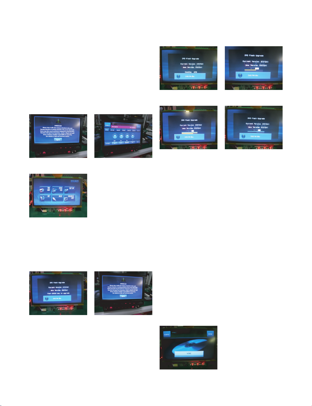
DVD FIRMWARE UPDATE GUIDE
Copyright © 2007 LG Electronics. Inc. All right reserved.
Only for training and service purposes
LGE Internal Use Only
Step 1 : Change into DVD source
- Power on then press open button to open LCD
monitor.
- Touch agree button
- LAN9700R set shows tuner screen.
- Change into DVD source by pressing a SRC key
or select DVD source in Source screen.
- We can enter source screen by touch source
button at left & upper corner.
Step 2 : Insert DVD F/W Disc
- Insert a DVD F/W Update Disc
- Press an enter key of front panel after DVD F/W
Disc popup shows
Step 3 : DVD F/W updating
- DVD F/W update begins
(Reading step --> Erasing step --> Writing step
--> Verifying step)
- DONOT STOP or POWER OFF during F/W
updating.
Step 4 : Remove DVD F/W disc
- If the verifying step is finished then display
screen is changing and it shows a disc reading
popup and DVD F/W disc popup again.
- eject the disc by pressing a eject button.
- Set power off
Step 5 : Additional Info
- If you see noises such as horizontal lines on
screen then take below procedure
step A) Power on and change into DVD source
and remove disc.
step B) Press pause button of remote controller
for 10 sec.
step C) NTSC or PAL popup shows.
step D) Repeat step B), step C) until NTSC/PAL
popup you want shows
step E) We recommend NTSC mode.
step F) Set power off
Agree screen
Source screen
Tuner screen
Reading step
Writing step
Writing step
Verifying step
Erasing step
DVD F/W disc popup Enter key
Page 7

1-6
SOFTWARE REPLACE METHOD
Copyright © 2007 LG Electronics. Inc. All right reserved.
Only for training and service purposes
LGE Internal Use Only
<Run Update Program: Remote controller>
1. After booting the unit without the Navi SD card, insert the Update SD card.
2. Enter the setup screen and press the Enter key on the remote controller for a long time.
(About 5~8 seconds)
3. Update Program will be displayed on the screen.
<Run Update Program: When there is no remote controller >
1. After booting the unit without the Navi SD card and entering the setup screen, press the Arrow key
on the right side of the front panel for more than 5 seconds. (Press and wait for 5 seconds after
switching to up direction)
Or press the Enter key on the remote controller for a long time.
2. Windows Explorer will be displayed.
3. Insert the Update SD card.
4. After selecting my device / SD memory, run Hobbiton.
<How to update the application SW >
1. Run the Update Program.
2. Press the Application button.
3. When you see the Copy Completed (xxx files/xxx files) message, the Application SW update is completed. If you see the message saying xxx file(s) Missed, it means that some files are not copied.
Reset the power and then repeat from step 1.
4. When it is completed, press the Exit button.
5. Remove the SD card and then reboot the unit.
<How to update Micom >
1. Run the Update Program.
2. Press the Micom button.
3. The progress increases by 10%.
4. When the progress reaches 100%, Program Ok !!! message will be displayed and Micom update is
completed.
5. If there are no files to update, message saying “File could not be opened !!!” will be displayed.
6. When the process is completed, press the Exit button.
7. Remove the SD card and then reboot the unit.
<How to update BT firmware >
1. Run the Update Program.
2. Press the BT Handsfree button.
3. When “BT Firmware Upgrade Completed.” Is displayed, update is completed. (This is irrelevant from
the displayed %. If the “BT Firmware Upgrade Completed.” message is displayed even when the displayed progress is not 100%, it is completed.)
Page 8

1-7
Copyright © 2007 LG Electronics. Inc. All right reserved.
Only for training and service purposes
LGE Internal Use Only
4. When the update fails, it will automatically retry the update again. When the process is not completed even when the progress is over 200%, update has failed. In this case, press the Exit button and
then reset the unit to retry the update.
5. If update is not required, “BT Firmware Upgrade Unnecessary.” Message will be displayed. In this
case press the Exit button or update other SW.
But, you cannot update the Kernel in this condition. You must reset the unit to update the
Kernel.
6. If there is no BT firmware in the SD card, “No BT Files” message will be displayed.
7. When it is completed, press the Exit button.
8. Remove the SD card and then reboot the unit.
* Reference
- Update of BT firmware can take maximum of 10 minutes. If difference between the version of the
existing firmware and the new version is small, the time to update is reduced. Generally, it requires
about 5~6 minutes.
- The reason the Micom firmware update takes longer than the time to update other SW is because
it requires more time to read the software to compare to the existing version.
- To update the BT firmware for other models, you must first disassemble the unit. But for
LAN9700R, you can update the unit using only the SD card without having to disassemble the unit,
this is a major improvement in work productivity.
<How to update Kernel >
1. Run the Update Program.
2. Press the Kernel NB0 button.
3. Wait until “Kernel NB0 Upgrade Completed” message is displayed.
4. After pressing the Exit button, remove the SD card and insert the original SD card in Navi to reboot
the unit.
* Caution: If you turn off the power or press the Exit button while updating the Kernel, it may be
impossible to recover.
<How to update App, Micom, BT firmware and Kernel all at once >
1. Run the Update Program.
2. Press the Update All button. It will be updated in the order of Application -> Micom -> BT -> Kernel.
3. After updating the BT firmware,
Notice: Kernel not completed.
Reset and then Upgrade Kernel
When the above message is displayed, Kernel update is not completed yet.
In this case, reset the unit and update the Kernel.
4. When “ALL SW Upgrade Completed.” Is displayed, the update for all SW is completed. Press the
Exit button and then remove the SD cards. Insert the Navi SD card and then reset the unit.
Page 9
1-8
Copyright © 2007 LG Electronics. Inc. All right reserved.
Only for training and service purposes
LGE Internal Use Only
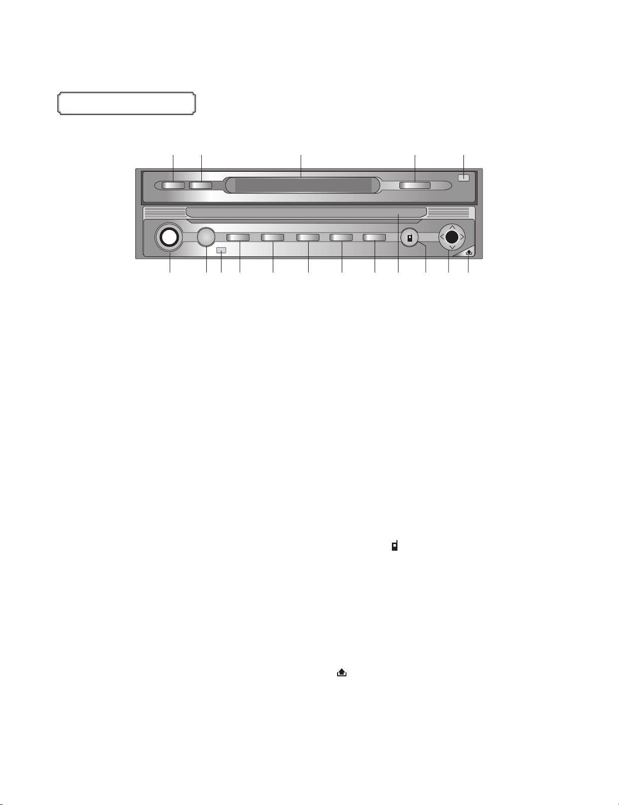
LOCATION OF CUSTOMER CONTROLS
HEAD UNIT FRONT
1. FLIP
Turn the LCD panel horizontally temporarily
when the LCD panel is upright.
2. TILT
Adjust the monitor angle.
3. Display window
4. OPEN/CLOSE
Open (or Close) the monitor.
5. DIMMER SENSOR
6. VOL (Volume knob)
• Adjust the volume.
• Power on (Press it.)
• Power off (Press a long time.)
• Mute (Press a short time.)
7. SRC (Source)
Change the sources.
8. Remote sensor
9. RSE
(Rear Seat Entertainment)
10. BAND
• Select the band.
11. RDS
• Select the TA on/off.(Press a short time.)
• Select the AF on/off.(Press a long time.)
12. EQ
Select various equalizer curves.
13. EJECT
Eject a disc from the unit.
14. Disc slot
15. PHONE ( )
Select the bluetooth mode.
16. Arrow keys (up/down/left/right)
• Select the folders.
• Select the menus.
• Skip (Push a short time.)
• Seek (Push a short time.)
• Enter
17.
Detatches the control panel.
12 3 4 5
FLIP TILT OPEN
VOL
SRC
EJECT
R
TA/AF
EQRDSBANDRSE
6789101112 13 1514 16
17
Page 10

1-9
Copyright © 2007 LG Electronics. Inc. All right reserved.
Only for training and service purposes
LGE Internal Use Only
HEAD UNIT MONITOR
18. LCD
19. WIDE
Changes the screen mode.
20. NAVI
Moves to the map screen.
21. MENU
Moves to the navigation menu.
FLIP TILT CLOSE
WIDE
NAVI
MENU
1918 20 21
Page 11
1-10
Copyright © 2007 LG Electronics. Inc. All right reserved.
Only for training and service purposes
LGE Internal Use Only
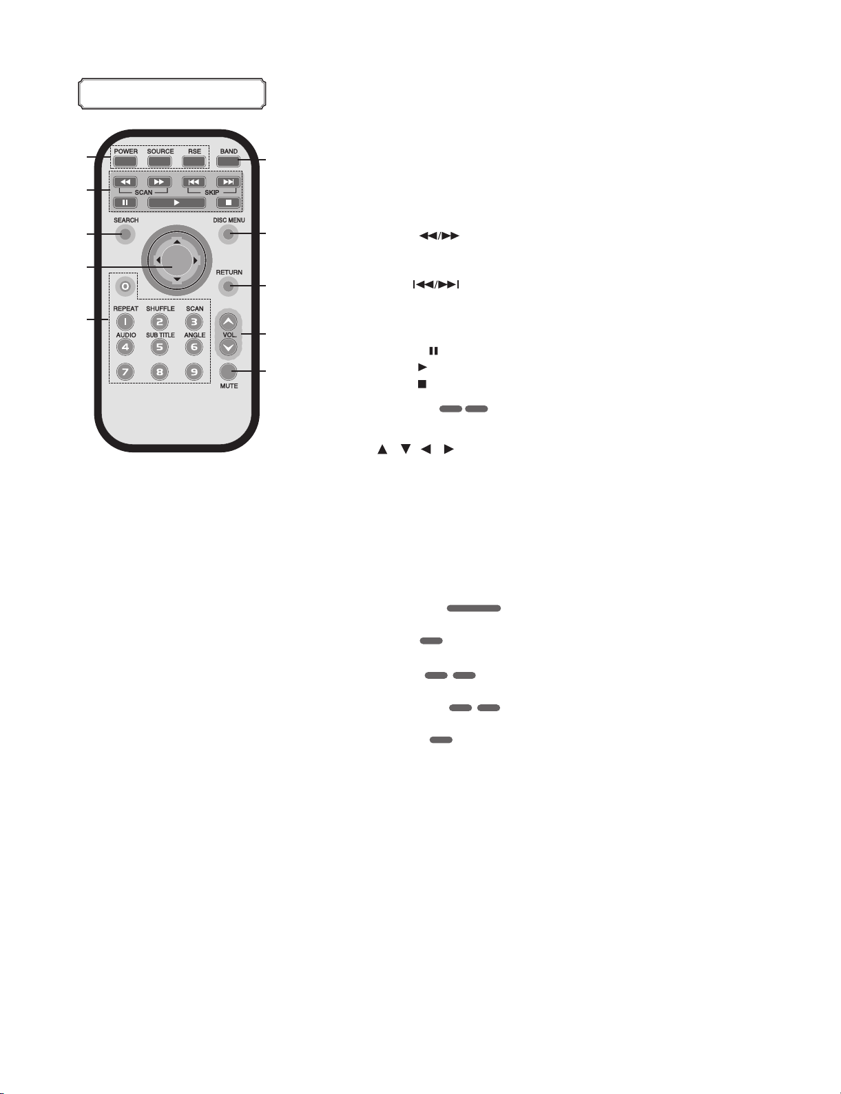
REMOTE CONTROL
1. POWER
Switches the unit ON/OFF.
SOURCE
Selects a source.
RSE (Rear Seat Entertainment)
2. SCAN
• Backward (Forward) search playback.
• Tunes manually radio station.
SKIP
• Moves to next (previous) chapter, track or file.
• Returns to the beginning of the current chapter, track or file.
• Tunes automatically radio station.
PAUSE
PLAY
STOP
3. SEARCH
Select chapter or title.
4. / / / (up/down/left/right)
Select an item in the menu.
ENTER
Confirms menu selection.
5. 0-9 number buttons
• Selects numbered items in the menu.
• Selects a stored radio station frequency(1-6).
REPEAT
• Repeat chapter, track, title or file.
SHUFFLE
• Plays tracks or files in random order.
SCAN
• Plays the first 10 seconds of all track.
AUDIO
• Select audio language.
SUBTITLE
• Select audio subtitle language.
ANGLE
• Select a DVD camera angle if available.
6. BAND
Select FM and MW(AM) bands.
7. DISC MENU
Accesses the menu on a DVD disc.
8. RETURN
Displays the disc menu with PBC.
9. VOLUME
Adjust the volume level.
10. MUTE
Mute the volume.
1
2
6
3
7
4
8
5
9
10
VCDDVD
CD/MP3/WMA
CD
DVD DivX
DVD DivX
DVD
Page 12
1-11
Copyright © 2007 LG Electronics. Inc. All right reserved.
Only for training and service purposes
LGE Internal Use Only
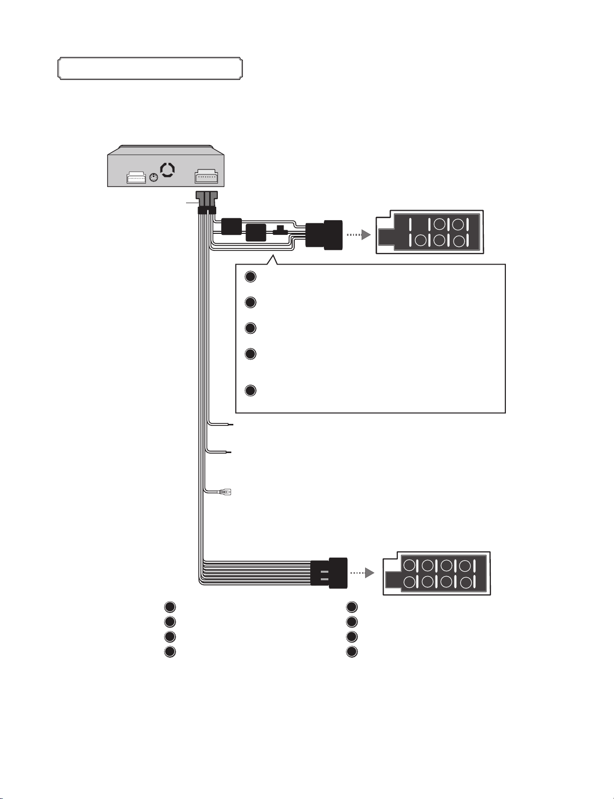
CONNECTING THE SYSTEM
B8
B7
B6
B5
A8
A7
A6
A5
A4
B4
B3
B2
B1
* Connecting the system
Power cord
Vehicle connector
A5
A7
A4
A6
A8
Yellow
TO BATTERY (+)- To the car battery, continuos +12 V DC.
Blue
POWER ANTENNA- To the power antenna
Orange
DIMMER-This lead is for the dimmer line connection.
Red
TO IGNITION-To the terminal from which the power is
supplied when the ignition switch is set to ACC.
Black
GROUND (-) - To the car body.
Blue/White
REMOTE ON-To the amplifier remote on.
Brown
HAND BREAK- Be sure to wire the hand break (parking break)
for safety and preventing accidents.
: Violet : Rear Right +
: Violet/ Black Stripe : Rear Right -
: Gray : Front Right +
: Gray / Black Stripe : Front Right -
Pink
REVERSE GEAR - When connecting the rear view camera, use
the reverse lead. Use a Reverse Extension if
needed.
Speaker connector
B1
B2
: White : Front Left +
: White/Black Stripe : Front Left -
: Green : Rear Left +
: Green/ Black Stripe : Rear Left -
B5
B3
B4
B7
B6
B8
Page 13
1-12
Copyright © 2007 LG Electronics. Inc. All right reserved.
Only for training and service purposes
LGE Internal Use Only
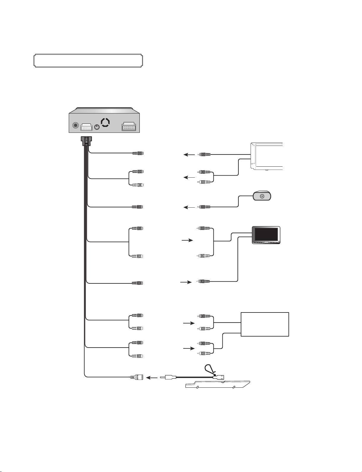
CONNECTING THE SYSTEM
* Connecting to serarately sold auxiliart device
To VIDEO IN
To AU D IO IN
To VIDEO IN
To A UD I O O UT
To VIDEO OUT
To A UD I O OUT
To AUDIO OUT
AUX V
(AUX Video)
AUX-R
(AUX Right)
AUX-L
(AUX Left)
CAM V
(Camera Video)
RSE R
(Rear Seat
Entertainment
Right)
RSE L
(Rear Seat
Entertainment
Left)
RSE V
(Rear Seat
Entertainment
Video)
RR
(Rear Right)
RL
(Rear Left)
FR
(Front Right)
FL
(Front Left)
To VIDEO OUT
To AUDIO OUT
To VIDEO OUT
To AUDIO IN
To VIDEO IN
To AUDIO IN
To AUDIO IN
Auxiliart Device
(CAR TV, etc)
Rear view camera
(Sold seperately)
Monitor for rear seat
(Sold seperately)
Amplifier (Receiver)
(Sold seperately)
To MIC IN
Microphone
Page 14

2-1
Copyright © 2007 LG Electronics. Inc. All right reserved.
Only for training and service purposes
LGE Internal Use Only
SECTION 2
CABINET & MAIN CHASSIS
CONTENTS
EXPLODED VIEWS ....................................................................................................................2-2
1. CABINET AND MAIN FRAME SECTION ................................................................................2-3
2. ACCESSORY SECTION ...........................................................................................................2-5
Page 15
Copyright © 2007 LG Electronics. Inc. All right reserved.
Only for training and service purposes
LGE Internal Use Only
2-3 2-4
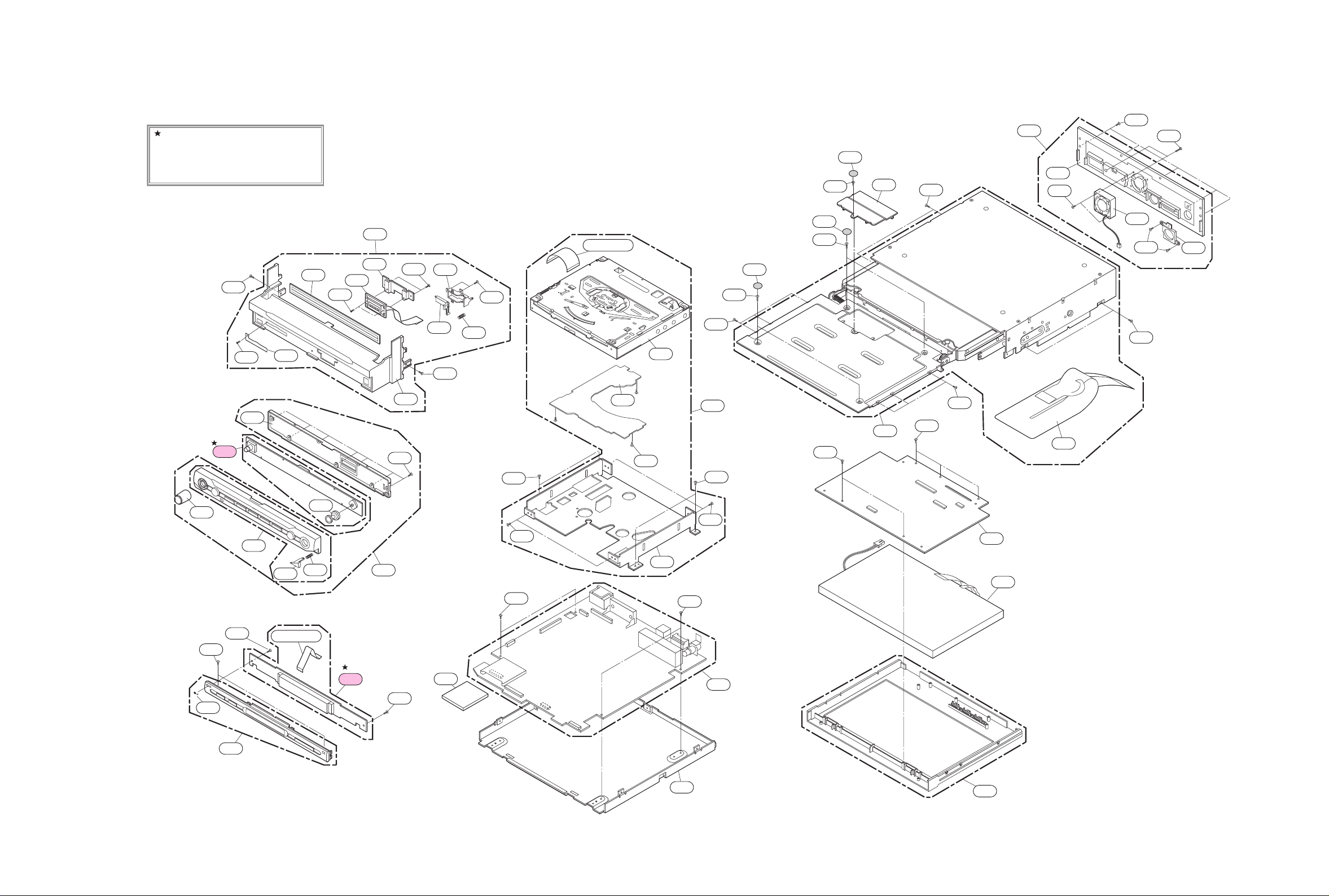
EXPLODED VIEWS
1. CABINET AND MAIN FRAME SECTION
A41 is consisted of
FRONT KEY + SEG LCD Assembly.
Therefore, 2EA's PCB Assembly is
supplied if request purchase by
A41's P/No.
266
451
462
A41
254
259
454
267
A48
268
260
450
461
272
255
451
256
461
452
CABLE40
A02
460
A01
451
A00
452
450
290
290
450
450
451
290
285
A47
452
450
451
A49
286
455
288
452
287
452
452
455
289
250
279
459
461
A53
A54
253
252
CABLE20
251
A41
A40
461
275
452
452
273
270
452
A42
A55
452
A46
A43
Page 16
Copyright © 2007 LG Electronics. Inc. All right reserved.
Only for training and service purposes
LGE Internal Use Only
2-5 2-6
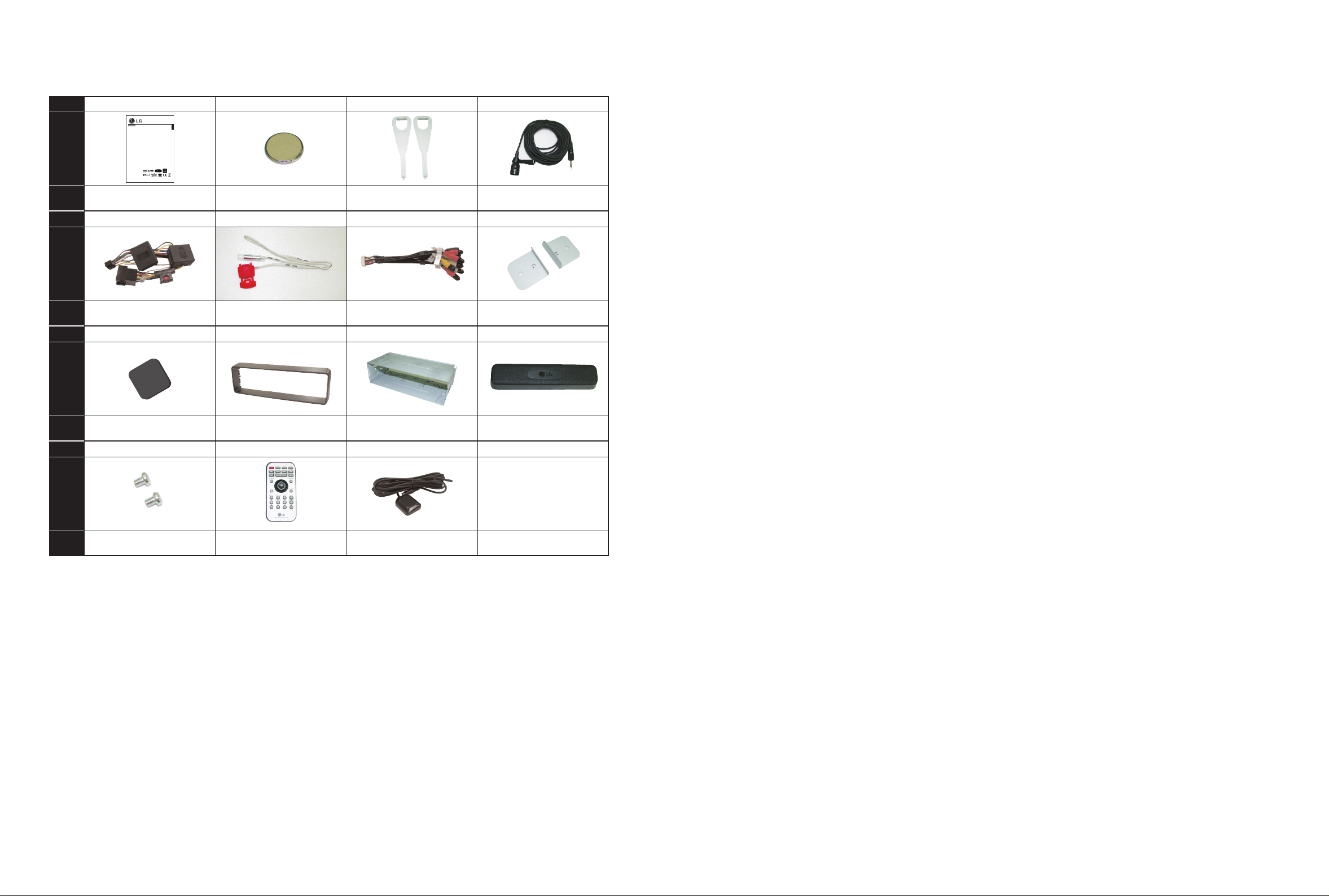
LOC.No.
DESCRIP
TION
Manual Assembly
801 808 818 831
Remote Control Battery Lever Microphone
Power cord
835 837 839 840
Reverse Extension Code
RCA and microphone
connector
Brackets
Metal sheet
842 843 845 846
Trim ring Installation sleeve Protective Case
852 900 A60
Remote Control
* OPTIONAL PART
GPS AntennaRound Head Screw
LOC.No.
DESCRIP
TION
LOC.No.
DESCRIP
TION
LOC.No.
DESCRIP
TION
2. ACCESSORY SECTION
LAN9700R
ENGLISH
In Dash Navi & Infotainment System
with Bluetooth
Read the manual carefully before using the unit.
Page 17

Copyright © 2007 LG Electronics. Inc. All right reserved.
Only for training and service purposes
LGE Internal Use Only
3-1
SECTION 3
ELECTRICAL
CONTENTS
ELECTRICAL TROUBLESHOOTING GUIDE.................3-2
1. NO RESPONSE WHEN POWER IS
TURNED ON ............................................................3-2
2. DISC IN/OUT DYSFUNCTION.................................3-3
3. NO RESPONSE ON LCD SCREEN ........................3-4
4. TILT MECHA OPEN/CLOSE DYSFUNCTION .........3-5
5. NO SOUND ..............................................................3-6
6. NO GPS ...................................................................3-7
BLOCK DIAGRAMS ........................................................3-8
1. OVERALL BLOCK DIAGRAM[WITH I/F] .................3-8
2. BLOCK DIAGRAM-[H/W] .......................................3-10
3. BLOCK DIAGRAM-[S/W] .......................................3-12
4. MAIN PCB BLOCK DIAGRAM...............................3-14
5. MAIN IN/OUT BLOCK DIAGRAM ..........................3-16
6. MAIN POWER BLOCK DIAGRAM.........................3-18
7. TFT LCD BLOCK DIAGRAM..................................3-20
8. TFT LCD POWER BLOCK DIAGRAM...................3-22
9. GPS BLOCK DIAGRAM.........................................3-24
10. GPS POWER BLOCK DIAGRAM ........................3-26
CIRCUIT DIAGRAMS ....................................................3-28
1. MAIN_CPU CIRCUIT DIAGRAM ...........................3-28
2. MAIN_MEMORY, ETC. CIRCUIT DIAGRAM .........3-30
3. MAIN_BT, DVD, USB, ETC. CIRCUIT DIAGRAM .3-32
4. MAIN_AUDIO MICOM CIRCUIT DIAGRAM ..........3-34
5. MAIN_DIRAMA, TUNER CIRCUIT DIAGRAM.......3-36
6. MAIN_RAC, LINE DRIVER CIRCUIT DIAGRAM...3-38
7. MAIN_POWER CIRCUIT DIAGRAM .....................3-40
8. FRONT KEY_KEY FRONT CIRCUIT DIAGRAM...3-42
9. TFT LCD_VP78 LCD CIRCUIT DIAGRAM............3-44
10. TFT LCD_POWER, TSC2003, BLU, CONNECTOR
CIRCUIT DIAGRAM .............................................3-46
11. SEG LCD_SEG LCD CIRCUIT DIAGRAM ..........3-48
12. GPS_GPS CIRCUIT DIAGRAM...........................3-50
•
WAVEFORMS..........................................................3-52
•
CIRCUIT VOLTAGE CHART ...................................3-58
PRINTED CIRCUIT DIAGRAMS ...................................3-62
1. MAIN P.C. BOARD (TOP VIEW) ............................3-62
2. MAIN P.C. BOARD (BOTTOM VIEW) ....................3-64
3. FRONT KEY & SEG LCD P.C. BOARD
(TOP VIEW)............................................................3-66
4. FRONT KEY & SEG LCD P.C. BOARD
(BOTTOM VIEW)....................................................3-66
5. GPS P.C. BOARD (TOP VIEW) .............................3-66
6. GPS P.C. BOARD (BOTTOM VIEW) .....................3-66
7. TFT LCD P.C. BOARD (TOP VIEW) ......................3-68
8. TFT LCD P.C. BOARD (BOTTOM VIEW) ..............3-69
Page 18
Copyright © 2007 LG Electronics. Inc. All right reserved.
Only for training and service purposes
LGE Internal Use Only
3-2
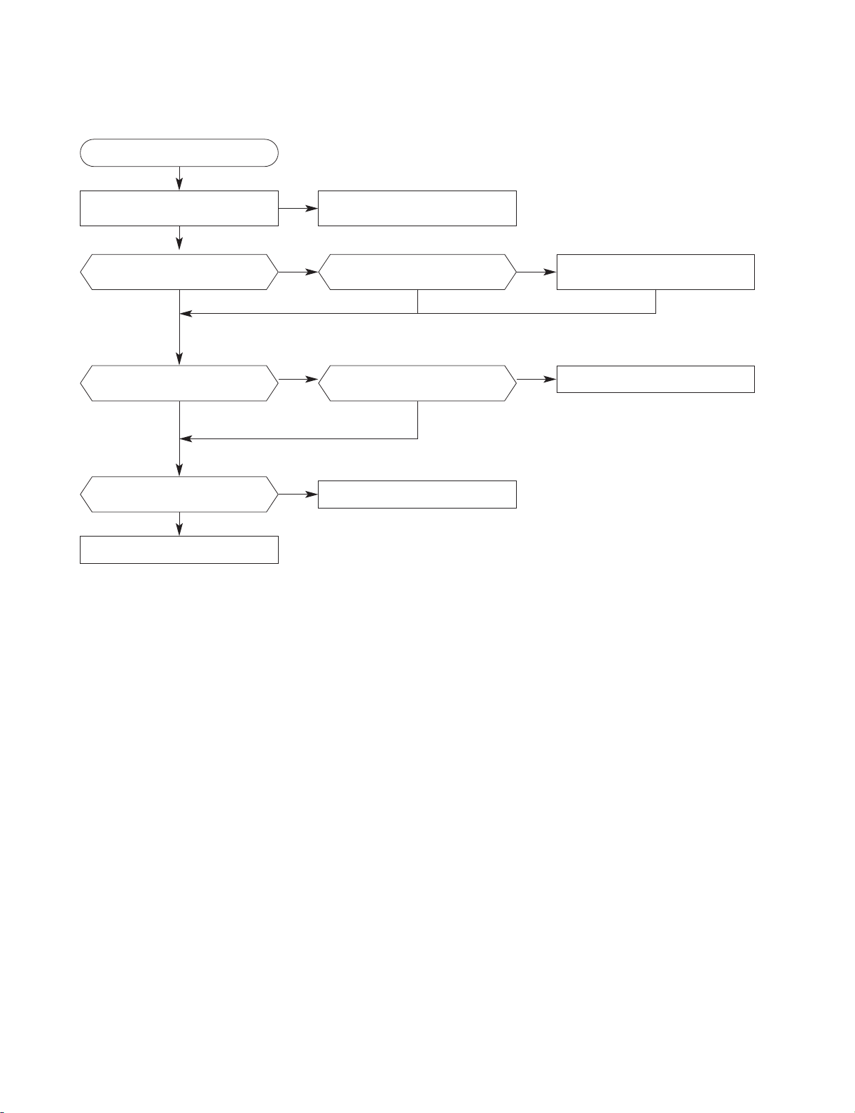
ELECTRICAL TROUBLESHOOTING GUIDE
1. No response when POWER is turned ON
YES
YES
YES
YESYES
NO
Connect power connector
NO
Is the front panel installed?
YES
Is the front FPC connection and
condition (disconnection) abnormal?
NO
Start from near IC100 and IC102. (Check
and refer to voltage wave form diagram.)
NO
Replace fuse.
NO NO
Is it operating normally after
the installation?
NO
Connect FPC.
Replace if disconnected
No response when
power is turned on.
Is the fuse normal?
Is the power cable normally
connected to CN103?
Is the LED turned on?
YES
Do you hear the sound
when setting the Beep ON?
Check whether the TILT
MECHA is normal.
Page 19
Copyright © 2007 LG Electronics. Inc. All right reserved.
Only for training and service purposes
LGE Internal Use Only
3-3
2. Disc in/out dysfunction
YES
YES
YES
YES
YES
YES
NO
CN401 2, 5~11, 6~19, 31
NO
37, 41, 49
NO
Recheck after connecting
NO
Check the peripheral circuit of CN403 and
whether other keys are pressed.
NO
Replace deck
When operating the Eject key,
do you hear the beep sound?
Disc in/out dysfunction
Can you see the LG logo on the RSE screen?
Is the power connected to CN401?
Is CN604 FFC normally connected?
Does the disc eject pop up?
Check whether there is anything
wrong with the deck.
Page 20
Copyright © 2007 LG Electronics. Inc. All right reserved.
Only for training and service purposes
LGE Internal Use Only
3-4
3. No response on LCD screen
YES
YES
YES YES YES
YES
NO NO
Replace IC702
NO
YES
YES
NO
NO NO
Replace IC501
NO
Check whether installed and
reinstall if necessary
NO
Replace IC501
No response on LCD (touch) screen
Was Front Panel installed?
Is the wave form of M2-12
normal?
Is the 65 pin of IC501 high
(5V)?
When you touch the screen,
do you hear the beep sound?
Is the wave form of M2-10
normal?
YES
Is the wave form of M4-7
and M4-8 normal?
Is the wave form of M2-5, 6,
7, 8 and 11 normal?
Is there still no response
after updating the SW?
IC701
YES
Replace IC200 or main board
Page 21
Copyright © 2007 LG Electronics. Inc. All right reserved.
Only for training and service purposes
LGE Internal Use Only
3-5
4. Tilt MECHA open/close dysfunction
YES
YES
YES YES YES
YES
NO NO
Check the connection between
the sub LCD FFC and front FPC.
NO
YES
NO
Replace IC501
NO
Recheck after normal
connection
NO
Replace SW
Tilt MECHA open/close dysfunction
Is the connection between
CN402 and FPC normal?
Is it 5V when the CN402 (No.6 and 8)
pin is open and 0V when closed?
Is the tilt MECHA SW
operating normally?
When you press the button, do
you hear the beep sound?
When entering a different key on the front
panel, do you hear the beep sound?
YES
Is the output of 59, 60 and
61 pin of IC501 normal?
Replace tilt MECHA
Page 22

Copyright © 2007 LG Electronics. Inc. All right reserved.
Only for training and service purposes
LGE Internal Use Only
3-6
5. No sound
YES
YES
YES
YES
YES
NO NO
Replace power AMP (IC602)
Check IC601->IC602
connection DAC output pattern
NO
YES
NO
Replace TR (Q601)
NO
Check speaker output
connection
No sound
Is the audio (IC601) input power
V3.3_D, V3.3_A normal?
Check LDO power
Is there audio DSP (IC601)
output?
Is there power AMP (IC602)
output?
Is there power AMP input?
Is the Q601 output
(DIRANA_1.8V) normal?
NO
Replace XTAL (X601)
Is the XTAL (X601)
wave form normal?
YES
YES
Replace audio DSP (IC602)
Page 23

3-7
Copyright © 2007 LG Electronics. Inc. All right reserved.
Only for training and service purposes
LGE Internal Use Only
6. No GPS
YES
YES
YES
YES
YES
NO
Check CN102
NO
Check Main B/D power supply (JT483)
NO
Check VCXO output (X100 PIN3)
NO
Check uart path
Is data transferred from module?
(CN102 PIN4 or TP Tx)
Does ACQ_CLK signal appear?
(TP ACQ_CLK)
Is power supplied to MODULE?
(CN102 PIN 1 or TP VDD)
NO GPS
CN102 connection?
REPLACE GPS MODULE
Page 24

Page 25

3-8 3-9
BLOCK DIAGRAMS
1. OVERALL BLOCK DIAGRAM[WITH I/F]
Copyright © 2007 LG Electronics. Inc. All right reserved.
Only for training and service purposes
LGE Internal Use Only
GPS Module
FM/AM ANT
CVBS, AUDIO(L/R)
AUX IN ( CVBS, AUDIO L/R)
REAR CAMERA
MIC
JAK401
ANT601
CN601
LAN9700R
UNIT
B+,ACC,GND
REMOTE ON
POWER ANT
REVERSE GEAR
HAND BREAK
DIMMER
F/L+
F/L-
CN103
F/R+
F/R-
R/L+
R/L-
AUDIO PRE-OUT ( F/L,F/R,R/L,R/R)
AUDIO PRE-OUT ( NON-FAD L/R)
R/R+
R/R-
Page 26

3-10 3-11
2. BLOCK DIAGRAM-[H/W]
GPS
DVD
MODULE
MPU
AUDIO
MICOM
POWER
AMP
DiRANA
RDS
TMC
BOOST AMP
NJM2792
BT
DDR SDRAM
64MB
[1V8]
I.MX31
[1V5, 1V8, 3V0]
[5V]
SAF6630H
[1V8, 3V3]
F1M22
[3V0]
[1V8]
UART
ATAPI
I2S
I2S I2S
SPI
I2S
I2S
UART
IR
4X5
CCIR656
I2S
SPI
CCIR656
A/AUDIO
NAND FLASH
64MB
[1V8]
UART
I2S
I2S
TOUCH PANEL
7" TFT LCD
480X234
ANALOG / LED
Sub
LCD
Comtrol
LCD
Control
Touch
Control
CVBSX2
UART/ETH
F/L, F/R, R/L, R/R
F/L, F/R, R/L, R/R
REAR CAMERA(CVBS)
AUX VIDEO(CVBS)
ACC, H-BRAKE,
REAR GEAR
DEBUG
KEY
TILT MECHA
IR
PRE OUT
SPEAKER OUT
MIC IN
A/V
RSE OUT
VIDEO(CVBS)
AUDIO R/L
Copyright © 2007 LG Electronics. Inc. All right reserved.
Only for training and service purposes
LGE Internal Use Only
Page 27

3-12 3-13
3. BLOCK DIAGRAM-[S/W]
Copyright © 2007 LG Electronics. Inc. All right reserved.
Only for training and service purposes
LGE Internal Use Only
Graphical User Interface
DVD/CD/
MP3/WMA
DVD
Function
& Comm
(SPI)
Tuner
GUI Application
Tuner/Setup
Function
Audio Micom
Comm.
(UART)
AUX
Rear
Camera
Setup
System Manager
Popup
Program
Update
WIN32 APIs, COREDLL, ...
System
Logger
Bluetooth
GUI
Manager
SW
Debugging
TCP / IP / EWC
PPP
3D/Full
Navigation GUI
Route
Guidance
Map
Matching
Route
Planning
Navigation
menu GUI
3D/Full_Navi
Main Module
Database
Application
(distination/POI)
Database
Manage
-ment
Audio
CODEC
DAL
Kernel
Library
OAL/
Bootloader
Display
Driver
GWES
Keypad
Driver
RemoconKeyLCD
IrDA
Driver
FileSystem
Manager
Touch
Screen
Touch
Screen
NAND
Flash
File
Drivers
(FAT32...)
Hardware
SD
Card
I2S
Driver
I2S
UART
Driver
UART
Device
Manager
SPI
Driver
SPI
Ethernet
Driver
Ethernet
Page 28

3-14 3-15
4. MAIN PCB BLOCK DIAGRAM
Copyright © 2007 LG Electronics. Inc. All right reserved.
Only for training and service purposes
LGE Internal Use Only
LCD FRONT : 3EA
LCD MAIN : 3EA
Page 29

3-16 3-17
5. MAIN IN/OUT BLOCK DIAGRAM
Copyright © 2007 LG Electronics. Inc. All right reserved.
Only for training and service purposes
LGE Internal Use Only
SUB-LCD
SENSOR
LCD
BOARD
COL 2, ROW 2
TOUCH
PANEL
POWER
LCD
CON
BUTTON
6EA
INTERRUPT
CCIR656
COL 3, ROW 3
GND
SPI
I2C
IRQ
POWER
5V0
9V
10V
VIDEO
I2C 1
KEY
MATRIX
SPI
DECK
POWER
1V2
3V3
5V0
8V0
POWER
3V0
DEBUG
JTAG UART Ethernet
MAIN
BOARD
GPS
UART
1. PRE OUT (F/R : L/R)
2. REAR OUT (AV 1)
3. MIC IN
4. AUX IN
5. CAMERA IN
1. BUP
2. ACC
3. DIMMER
4. REMOTE
5. POWER ANT
6. H.BRAKE
7. REVERSE GEAR
8. SPEAKER OUT (F/R : L/R)
COL 3, ROW 5
IR
FRONT
DETECT
Page 30

3-18 3-19
6. MAIN POWER BLOCK DIAGRAM
Copyright © 2007 LG Electronics. Inc. All right reserved.
Only for training and service purposes
LGE Internal Use Only
Page 31

3-20 3-21
7. TFT LCD BLOCK DIAGRAM
Copyright © 2007 LG Electronics. Inc. All right reserved.
Only for training and service purposes
LGE Internal Use Only
DIMMING
5V
Analog RGB
ETC
3.3V
2.5V
BLU(LED type)
LCD PANEL
(INNOLUX :
AT070TN07 V.2)
5V
15V
VP78
-10V
9.0V
TOUCH
PANEL
3.0V
X+
X-
Y+
Y-
KEY
LED
C2003
TS
CCIR656, CVBS*2
KEY
PENIRQ
IIC
IIC
Key
Matrix
5.0V
9.0V
MAIN
BOARD
FRONT LCD
SEG
FRONT LCD
Controller
PT6524
SPI
Page 32

3-22 3-23
8. TFT LCD POWER BLOCK DIAGRAM
Copyright © 2007 LG Electronics. Inc. All right reserved.
Only for training and service purposes
LGE Internal Use Only
9.0V
Main BD.
5.0V
SW
DC-DC
SW
SEG
BACKLIGHT
KEY LED
LCD
BACKLIGHT
LCD PANEL
VCOM/VGH/VGL
RGB AMP.
3.3V
3.0V
TFT LCD BD.
SEG DRIVER
IC
VP
78
2.5V
T/S
Page 33

3-24 3-25
9. GPS BLOCK DIAGRAM
Copyright © 2007 LG Electronics. Inc. All right reserved.
Only for training and service purposes
LGE Internal Use Only
MAIN
UART
TRANCEIVER
MAX3232EIPWR
RESET
TC1301B
GSC3f/LP-7979
32.768KHz XTAL
FC-135
SAW FILTER
856561
24.5535MHz VCXO
DSB321SD
ANTENNA
LNA
UPC8231TK
Page 34

3-26 3-27
10. GPS POWER BLOCK DIAGRAM
Copyright © 2007 LG Electronics. Inc. All right reserved.
Only for training and service purposes
LGE Internal Use Only
5V VDD
3V BUP
2.8V
1.5V
2.8V
2.8V
LNA 2.8V
RTC 1.5V
RF 2.8V
BASE 2.8V
Page 35

3-28 3-29
CIRCUIT DIAGRAMS
1. MAIN_CPU CIRCUIT DIAGRAM
1
4
5
6
9
10
2
7
8
3
WAVEFORM
A
1
2
3
4
5
6
7
8
9
10
11
12
B C D E F G H I J K L M N O P Q RST
Copyright © 2007 LG Electronics. Inc. All right reserved.
Only for training and service purposes
LGE Internal Use Only
Page 36

3-30 3-31
2. MAIN_MEMORY, ETC. CIRCUIT DIAGRAM
15
19
14
16
17
18
22
23
13
21
20
11
12
WAVEFORM
A
1
2
3
4
5
6
7
8
9
10
11
12
B C D E F G H I J K L M N O P Q RST
Copyright © 2007 LG Electronics. Inc. All right reserved.
Only for training and service purposes
LGE Internal Use Only
Page 37

3-32 3-33
3. MAIN_BT, DVD, USB, ETC. CIRCUIT DIAGRAM
24
25
26
28
27
31
29
30
WAVEFORM
A
1
2
3
4
5
6
7
8
9
10
11
12
B C D E F G H I J K L M N O P Q RST
Copyright © 2007 LG Electronics. Inc. All right reserved.
Only for training and service purposes
LGE Internal Use Only
Page 38

43 3-35
4. MAIN_AUDIO MICOM CIRCUIT DIAGRAM
40
35
36
34
32
41
33
38
39
37
WAVEFORM
A
1
2
3
4
5
6
7
8
9
10
11
12
B C D E F G H I J K L M N O P Q RST
Copyright © 2007 LG Electronics. Inc. All right reserved.
Only for training and service purposes
LGE Internal Use Only
Page 39

5. MAIN_DIRAMA, TUNER CIRCUIT DIAGRAM
48
46
47
45
44
49
42
43
WAVEFORM
A
1
2
3
4
5
6
7
8
9
10
11
12
B C D E F G H I J K L M N O P Q RST
3-36 3-37
Copyright © 2007 LG Electronics. Inc. All right reserved.
Only for training and service purposes
LGE Internal Use Only
Page 40

6. MAIN_RAC, LINE DRIVER CIRCUIT DIAGRAM
A
1
2
3
4
5
6
7
8
9
10
11
12
B C D E F G H I J K L M N O P Q RST
3-38 3-39
Copyright © 2007 LG Electronics. Inc. All right reserved.
Only for training and service purposes
LGE Internal Use Only
Page 41

Copyright © 2007 LG Electronics. Inc. All right reserved.
Only for training and service purposes
LGE Internal Use Only
3-40 3-41
7. MAIN_POWER CIRCUIT DIAGRAM
54
52
53
50
51
WAVEFORM
A
1
2
3
4
5
6
7
8
9
10
11
12
B C D E F G H I J K L M N O P Q RST
Page 42

Copyright © 2007 LG Electronics. Inc. All right reserved.
Only for training and service purposes
LGE Internal Use Only
3-42 3-43
8. FRONT KEY_KEY FRONT CIRCUIT DIAGRAM
A
1
2
3
4
5
6
7
8
9
10
11
12
B C D E F G H I J K L M N O P Q RST
Page 43

Copyright © 2007 LG Electronics. Inc. All right reserved.
Only for training and service purposes
LGE Internal Use Only
3-44 3-45
9. TFT LCD_VP78 LCD CIRCUIT DIAGRAM
55
WAVEFORM
56
57
60
58
59
A
1
2
3
4
5
6
7
8
9
10
11
12
B C D E F G H I J K L M N O P Q RST
Page 44

Copyright © 2007 LG Electronics. Inc. All right reserved.
Only for training and service purposes
LGE Internal Use Only
3-46 3-47
10. TFT LCD_POWER, TSC2003, BLU, CONNECTOR CIRCUIT DIAGRAM
WAVEFORM
61
62
63
64
A
1
2
3
4
5
6
7
8
9
10
11
12
B C D E F G H I J K L M N O P Q RST
Page 45

Copyright © 2007 LG Electronics. Inc. All right reserved.
Only for training and service purposes
LGE Internal Use Only
3-48 3-49
11. SEG LCD_SEG LCD CIRCUIT DIAGRAM
A
1
2
3
4
5
6
7
8
9
10
11
12
B C D E F G H I J K L M N O P Q RST
Page 46

Copyright © 2007 LG Electronics. Inc. All right reserved.
Only for training and service purposes
LGE Internal Use Only
3-50 3-51
WAVEFORM
66
66
69
70
67
68
65
A
1
2
3
4
5
6
7
8
9
10
11
12
B C D E F G H I J K L M N O P Q RST
12. GPS_GPS CIRCUIT DIAGRAM
Page 47

Copyright © 2007 LG Electronics. Inc. All right reserved.
Only for training and service purposes
LGE Internal Use Only
3-52 3-53
[1] [2] [3] [4] [5]
[6] [7] [8] [9] [10]
[11] [12] [13] [14] [15]
[16] [17] [18] [19] [20]
[21] [22] [23] [24] [25]
• WAVEFORMS
[ MAIN PART ] _ 1~54
Page 48

Copyright © 2007 LG Electronics. Inc. All right reserved.
Only for training and service purposes
LGE Internal Use Only
3-54 3-55
[26] [27] [28] [29] [30]
[31] [32] [33] [34] [35]
[36] [37] [38] [39] [40]
[41] [42] [43] [44] [45]
[50][46] [47] [48] [49]
Page 49

Copyright © 2007 LG Electronics. Inc. All right reserved.
Only for training and service purposes
LGE Internal Use Only
3-56 3-57
[53] [54] [55][51] [52]
[57] [58] [59][56]
[62] [63] [64]
[60]
[61]
[68] [69] [70][67]
[ TFT LCD PART ] _
55~64
[65]
[ GPS PART ] _ 65~70
CN102_Pin4(TX)
[66]
IC106_J4, K4
IC106_TA IC106_TB X100_Pin3 X101
Page 50

Copyright © 2007 LG Electronics. Inc. All right reserved.
Only for training and service purposes
LGE Internal Use Only
3-58 3-59
• CIRCUIT VOLTAGE CHART
MODE
PIN NO.
23 DATA[3]
24 DATA[4]
25 DATA[5]
26 DATA[6]
27 DATA[7]
28 NC
29 NC
30 KEY_COL_0
31 KEY_ROW_0
32 KEY_COL_1
33 KEY_ROW_1
34 KEY_COL_2
35 KEY_ROW_2
36 SEG_DI
37 SEG_CLK
38 SEG_CON
39 SEG_CE
40 LCD_INTR
41 LCD_BL_CON
42 DIM_SENS
43 GND
44 5V
45 5V
46 5V
47 GND
48 GND
49 10V
50 10V
CN401
1 GND
2 CSI_CLK
3 GND
4 CSI_D[8]
5 CSI_D[9]
6 CSI_D[10]
7 CSI_D[11]
8 CSI_D[12]
9 CSI_D[13]
10 CSI_D[14]
11 CSI_D[15]
12 GND
13 DISC_IN
14 DVD_A_MUTE
15 DVD_RESET
16 SPI_TXD
17 SPI_RXD
18 SPI_CLK
19 SPI_CE
20 GND
21 RSE_V_MUTE
22 GND
23 A_BIT_CLK
24 GND
25 A_DATA
26 A_MCLK
VOLTAGE VOLTAGE VOLTAGE VOLTAGE VOLTAGE VOLTAGE
MODE
PIN NO.
MAIN
CN103
1 RL+
2 RR+
3 RL-
4 RR-
5 FL+
6 FR+
7 FL-
8 FR-
9 REVERSE
10 ACC
11 ANT_PWR
12 H_BRAKE
13 REMOTE_PWR
14 ILL
15 B+
16 GND
CN301
1DATA3
2 CMD
3VSS
4 VDD
5 CLK
6VSS
7DATA0
8DATA1
9DATA2
10 WP/CD
11 GND
12 DETECT
13 GND
CN302
1 TS_CLK
2 TS_IRQ
3TS_DATA
4LCD_SCL
5 LCD_SDA
6 LCD_RESET
7 GND
8 GND
9AUX_V
10 GND
11 CAM_V
12 GND
13 VSYNC
14 HSYNC
15 GND
16 V_CLK
17 GND
18 GND
19 LCD_POWER
20 DATA[0]
21 DATA[1]
22 DATA[2]
MODE
PIN NO.
27 A_LRCK
28 GND
29 CVBS
30 GND
31 1.2V
32 1.2V
33 1.2V
34 1.2V
35 GND
36 GND
37 3.3
38 5V_PU
39 5V_PU
40 5V
41 5V
42 5V
43 5V
44 GND
45 GND
46 GND
47 GND
48 GND
49 8V
50 8V
CN402
1 GND
2 GND
3 12V
4 12V
5 GND
6CLOSE_SW
7TILT_SW
8TILT_HOME
9LOAD_SEN
10 TILT_SEN
11 5V
12 TILT_CTR1
13 TILT_CTR2
14 TILT_CTR3
CN403
13V
2IR_REMOTE
3DISC_IN
4 KEY_ROW5
5 KEY_ROW4
6 KEY_ROW3
7 KEY_ROW2
8 KEY_ROW1
9KEY_COL5
10 KEY_COL4
11 K EY_COL3
12 8V
13 VOL_DOWN
14 VOL_UP
15 GND
MODE
PIN NO.
CN601
1 PREAMP_FL
2 PREAMP_FR
3 GND
4 PREAMP_RL
5 PREAMP_RR
6 GND
7 RSE_L
8 RSE_R
9 GND
10 AUX_L
11 AUX_R
12 GND
13 MIC_IN
14 GND
15 GND
16 CAM_V
17 GND
18 AUX_V
19 GND
20 RSE_V
JK401
1 CAL_RXD
2 CAL_TXD
35V
4 GND
5 GPS_TXD
6GPS_RXD
IC102
15
28
38
48
59
65
7 3.3
80
90
10 3.3
11 0
12 5
13 5
14 5
15 5
16 H/L
17 H/L
18 H/L
19 0
20 0
21 9
22 9
23 0
24 12
25 H/L
26 H/L
MODE
PIN NO.
MODE
PIN NO.
2 3.3
30
4 3.3
5 3.3
IC400
1NC
2NC
3RF
40
50
6NC
7NC
8 ANALOG
93
10 NC
11 NC
12 NC
13 0
14 NC
15 NC
16 1.8
17 NC
18 NC
19 0
20 H/L
21 NC
22 H/L
23 3
24 0
25 NC
26 H/L
27 NC
28 NC
29 H/L
30 H/L
31 NC
32 3
33 NC
34 0
35 H/L
36 H/L
37 H/L
38 H/L
39 H/L
40 H/L
41 NC
42 NC
43 NC
44 NC
45 NC
IC401
1 ANALOG
2 ANALOG
33
40
VOLTAGE
MODE
PIN NO.
50
60
70
83
IC402
16
26
3-6
46
5-6
6-6
7 H/L
8 H/L
9 H/L
10 H/L
11 H/L
12 H/L
13 H/L
14 H/L
15 0
16 3
IC403
1NC
2 H/L
30
4 H/L
53
IC404
1NC
2 H/L
30
4 H/L
53
IC405
10
2 H/L
3 H/L
4 H/L
5NC
6NC
7 H/L
8 H/L
9 H/L
10 0
11 H/L
12 H/L
13 H/L
14 NC
15 NC
16 H/L
17 H/L
18 H/L
19 0
20 3.3
VOLTAGE
MODE
PIN NO.
IC406
1NC
2 H/L
30
4 H/L
55
IC420
1NC
2H or L
30
4H or L
53
IC501
1 H/L
2 H/L
3 H/L
4 H/L
5 H/L
6NC
7 H/L
8NC
9NC
10 5
11 5.6
12 5or0
13 H/L
14 H/L
15 H/L
16 NC
17 NC
18 NC
19 NC
20 0
21 NC
22 5or0
23 5or0
24 5
25 5
26 5or0
27 5or0
28 5
29 5
30 5
31 NC
32 5
33 5
34 5
35 5
36 5
37 5
38 5
39 NC
40 5or0
41 5or0
42 H/L
VOLTAGE
MODE
PIN NO.
43 H/L
44 H/L
45 NC
46 H/L
47 5
48 H/L
49 H/L
50 5
51 0
52 5.6
53 5.6
54 5or0
55 NC
56 NC
57 5or0
58 5or0
59 5or0
60 5or0
61 5or0
62 5
63 5or0
64 5or0
65 5
66 5
67 5or0
68 5or0
69 5or0
70 H/L
71 H/L
72 5or0
73 5or0
74 5or0
75 5or0
76 H/L
77 H/L
78 5or0
79 5or0
80 5or0
81 H/L
82 5
83 NC
84 NC
85 NC
86 NC
87 0
88 5
89 H/L
90 5
91 H/L
92 H/L
93 0
94 H/L
95 H/L
96 5
97 0
VOLTAGE
MODE
PIN NO.
98 0
99 5
100 5
IC502
1NC
2 H/L
30
4 H/L
5 3.3
IC503
1 H/L
25
30
4NC
5NC
6NC
7 H/L
8NC
IC504
1NC
2 H/L
30
4 H/L
55
IC505
1NC
2 H/L
30
4 H/L
53
IC506
13
2 H/L
30
4 H/L
53
IC507
1 H/L
2 3.3
30
4 H/L
5 3.3
IC508
1NC
2 H/L
30
4 H/L
53
IC509
1 3.3
2 H/L
30
4 H/L
5 3.3
VOLTAGE
MODE
PIN NO.
IC510
1 3.3
2 H/L
30
4 H/L
5 3.3
IC511
1 3.3
2 H/L
30
4 H/L
5 3.3
IC512
1 H/L
2 H/L
30
4 H/L
55
IC514
15
2 H/L
30
4 H/L
55
IC515
1NC
2 H/L
30
4 H/L
53
IC601
1 1.8
2 1.62
3 1.62
4 1.62
5 1.62
6 1.62
7 1.62
8 3.3
9 3.3
10 0
11 1.62
12 1.62
13 1.62
14 1.62
15 1.62
16 1.62
17 1.62
18 1.62
19 1.62
20 1.8
21 0
22 0
23 0
24 NC
27 H/L
28 NC
IC205
13
23
30
43
53
IC207
13
23
30
43
53
IC305
10
2 H/L
3 H/L
4 H/L
5 H/L
6 H/L
7 H/L
8 H/L
9 H/L
10 0
11 H/L
12 H/L
13 H/L
14 H/L
15 H/L
16 H/L
17 H/L
18 H/L
19 0
20 3.3
IC306
1 3.3
2 H/L
30
4 H/L
5 3.3
IC307
1 3.3
2 H/L
30
4 H/L
5 3.3
IC308
1 3.3
2 H/L
30
4 H/L
5 3.3
IC309
1 3.3
Page 51

Copyright © 2007 LG Electronics. Inc. All right reserved.
Only for training and service purposes
LGE Internal Use Only
3-60 3-61
MODE
PIN NO.
80 0
81 0
82 0
83 0
84 0
85 0
86 0
87 3.3
88 NC
89 NC
90 H/L
91 NC
92 NC
93 NC
94 1.8
95 0
96 NC
97 NC
98 NC
99 NC
100 H/L
101 H/L
102 NC
103 NC
104 0
105 3.3
106 NC
107 NC
108 NC
109 NC
110 H/L
111 H /L
112 N C
113 N C
114 N C
115 N C
116 N C
117 N C
118 N C
119 N C
120 NC
121 0
122 1.8
123 H/L
124 H/L
125 1.8
126 0
127 H/L
128 H/L
129 0
130 0
131 CLK
132 CLK
133 1.8
134 NC
VOLTAGE VOLTAGE VOLTAGE VOLTAGE VOLTAGE VOLTAGE
MODE
PIN NO.
25 0
26 0
27 0
28 H/L
29 H/L
30 1.26
31 H/L
32 1.8
33 3.3
34 1.64
35 0
36 1.64
37 3.3
38 1.55
39 1.55
40 3.3
41 0
42 3.3
43 1.55
44 1.55
45 1.62
46 1.62
47 3.3
48 NC
49 H/L
50 NC
51 H/L
52 H/L
53 H/L
54 1.8
55 0
56 NC
57 H/L
58 NC
59 NC
60 1.8
61 0
62 H/L
63 H/L
64 H/L
65 H/L
66 H/L
67 H/L
68 0
69 3.3
70 NC
71 NC
72 H/L
73 H/L
74 H/L
75 NC
76 NC
77 NC
78 NC
79 0
MODE
PIN NO.
135 3.2
136 1.47
137 1.47
138 0
139 3.3
140 2.95
141 0
142 1.26
143 1.48
144 1.48
IC602
10
20
3 9.3
4 H/L
5 9.3
612
7 2.8
80
9 2.8
10 8.3
11 2.95
12 2.95
13 0
14 2.95
15 2.95
16 3
17 2.8
18 0
19 2.8
20 12
21 9.3
22 H/L
23 9.3
24 0
25 NC
IC603
10
2 0.64
3 7.1
4 2.84
5 2.84
6 4.26
7 2.84
8 2.84
9 7.1
10 0.64
11 0
12 7.8
13 7.1
14 2.84
15 2.84
16 8.5
17 2.84
18 2.84
MODE
PIN NO.
19 7.1
20 7.8
IC604
10
2 0.64
3 7.1
4 2.84
5 2.84
6 4.26
7 2.84
8 2.84
9 7.1
10 0.64
11 0
12 7.8
13 7.1
14 NC
15 2.84
16 8.5
17 NC
18 2.84
19 7.1
20 7.8
IC606
15
2 1.99
3 1.19
40
5 2.8
60
70
85
TFT LCD
IC701
1NC
2NC
3 H/L
4 H/L
5 H/L
6 3.3
70
80
9 2.5
10 0
11 3.3
12 0
13 NC
14 NC
15 ANALOG
16 NC
17 0
18 0
19 3.3
20 NC
21 NC
MODE
PIN NO.
MODE
PIN NO.
77 H/L
78 NC
79 NC
80 H/L
81 NC
82 NC
83 1.2
84 NC
85 NC
86 3.3
87 0
88 0
89 3.3
90 ANALOG
91 3.3
92 0
93 ANALOG
94 ANALOG
95 3.3
96 0
97 H/L
98 NC
99 NC
100 NC
101 NC
102 NC
103 NC
104 NC
105 NC
106 0
107 2.5
108 NC
109 NC
110 N C
111 N C
112 N C
113 N C
114 N C
115 N C
116 0
117 3.3
118 N C
119 N C
120 NC
121 NC
122 NC
123 NC
124 NC
125 NC
126 NC
127 NC
128 NC
SEG LCD
IC851
1 H/M1/M2/L
VOLTAGE
MODE
PIN NO.
2 H/M1/M2/L
3 H/M1/M2/L
4 H/M1/M2/L
5 H/M1/M2/L
6 H/M1/M2/L
7 H/M1/M2/L
8 H/M1/M2/L
9 H/M1/M2/L
10 H/M1/M2/L
11 H/M1/M2/L
12 H/M1/M2/L
13 H/M1/M2/L
14 H/M1/M2/L
15 H/M1/M2/L
16 H/M1/M2/L
17 H/M1/M2/L
18 H/M1/M2/L
19 H/M1/M2/L
20 H/M1/M2/L
21 H/M1/M2/L
22 H/M1/M2/L
23 H/M1/M2/L
24 H/M1/M2/L
25 H/M1/M2/L
26 H/M1/M2/L
27 H/M1/M2/L
28 H/M1/M2/L
29 H/M1/M2/L
30 H/M1/M2/L
31 H/M1/M2/L
32 H/M1/M2/L
33 H/M1/M2/L
34 H/M1/M2/L
35 H/M1/M2/L
36 H/M1/M2/L
37 H/M1/M2/L
38 H/M1/M2/L
39 H/M1/M2/L
40 H/M1/M2/L
41 H/M1/M2/L
42 H/M1/M2/L
43 H/M1/M2/L
44 H/M1/M2/L
45 H/M1/M2/L
46 H/M1/M2/L
47 H/M1/M2/L
48 H/M1/M2/L
49 NC
50 NC
51 NC
52 H/M1/M2/L
53 H/M1/M2/L
54 H/M1/M2/L
55 H/M1/M2/L
56 5(H)
VOLTAGE
MODE
PIN NO.
VOLTAGE
MODE
PIN NO.
C6 -
C7 H/L
C8 -
C9 -
C10 2.8V
D1 -
D2 -
D3 H/L
D4 2.8V
D5 GND
D6 GND
D7 -
D8 -
D9 -
D10 0V
E1 -
E2 -
E3 -
E4 2.8V
E7 -
E8 -
E9 -
E10 -
F1 -
F2 2.8V
F3 2.8V
F4 2.8V
F5 GND
F6 GND
F7 2.8V
F8 -
F9 -
F10 H/L
G1 H/L
G2 -
G3 -
G4 -
G5 -
G6 -
G7 -
G8 -
G9 -
G10 0V
H1 -
H2 -
H3 -
H4 -
H5 -
H6 0.8V
H7 -
H8 -
H9 -
H10 2.8V
J1 2.8V
J2 0V
VOLTAGE
MODE
PIN NO.
VOLTAGE
MODE
PIN NO.
P8 2.8V
P9 1.5V
P10 CLOCK
IC107 (TRANCEIVER)
1 7.5V
2 7.5V
35V
4 7.5V
50V
6 -6V
7 7.5V
80V
95V
10 0V
11 H/L
12 H/L
13 H/L
14 H/L
15 0V
16 5V
IC108 (LNA)
1 1V input
2 GND
3 2.8V
4 2.8V
5 GND
6 2.8V
22 ANALOG
23 NC
24 NC
25 0
26 0
27 3.3
28 NC
29 NC
30 0
31 0
32 0
33 0
34 1.7
35 NC
36 0
37 3.3
38 0
39 0
40 0
41 0
42 2.5
43 NC
44 H/L
45 H/L
46 H/L
47 H/L
48 H/L
49 H/L
50 H/L
51 H/L
52 H/L
53 H/L
54 H/L
55 3.3
56 0
57 NC
58 H/L
59 H/L
60 H/L
61 H/L
62 H/L
63 H/L
64 H/L
65 H/L
66 H/L
67 NC
68 NC
69 H/L
70 0
71 2.5
72 H/L
73 2.5
74 0
75 0
76 3.3
J3 -
J4 H/L
J5 H/L
J6 H/L
J7 H/L
J8 H/L
J9 H/L
J10 H/L
K1 H/L
K2 2.8V
K3 -
K4 H/L
K5 H/L
K6 H/L
K7 H/L
K8 H/L
K9 H/L
K10 H/L
L1 -
L2 2.8V
L3 2.8V
L4 GND
L5 GND
L6 GND
L7 GND
L8 GND
L9 GND
L10 CLOCK
M1 -
M2 2.8V
M3 2.8V
M4 2.8V
M5 2.8V
M6 2.8V
M7 2.8V
M8 2.8V
M9 2.8V
M10 2.8V
N1 0V
N2 GND
N3 GND
N4 GND
N5 GND
N6 GND
N7 GND
N8 GND
N9 GND
N10 GND
P1 H/L
P2 CLOCK
P3 -
P4 -
P5 GND
P6 RF SIGNAL
P7 GND
57 3.2(M1)
58 1.6(M2)
59 0(L)
60 ANALOG
61 H/L
62 H/L
63 H/L
64 H/L
GPS
CN102
1 Vcc(5V)
2 GND
3 Tx (H/L)
4Rx (H/L)
IC100 (LDO)
1 2.8V
2 2.8V
3 GND
4 1.2V
55V
6 2.8V
75V
85V
IC104 (LDO)
15V
2 GND
35V
4-
5 1.5V
IC106 (SiRF)
A1 GND
A2 -
A3 H/L
A4 -
A5 H/L
A6 H/L
A7 -
A8 -
A9 -
A10 1.6V
B1 -
B2 -
B3 2.8V
B4 1.5V
B5 2.8V
B6 -
B7 H/L
B8 -
B9 -
B10 2.8V
C1 -
C2 2.8V
C3 -
C4 2.8V
C5 2.8V
Page 52

Copyright © 2007 LG Electronics. Inc. All right reserved.
Only for training and service purposes
LGE Internal Use Only
3-62 3-63
MAIN PRINTED CIRCUIT DIAGRAMS
1. MAIN P.C. BOARD (TOP VIEW)
Page 53

Copyright © 2007 LG Electronics. Inc. All right reserved.
Only for training and service purposes
LGE Internal Use Only
3-64 3-65
2. MAIN P.C. BOARD (BOTTOM VIEW)
EAX38431201
Page 54

Copyright © 2007 LG Electronics. Inc. All right reserved.
Only for training and service purposes
LGE Internal Use Only
3-66 3-67
3. FRONT KEY & SEG LCD P.C. BOARD (TOP VIEW) 5. GPS P.C. BOARD (TOP VIEW)
6. GPS P.C. BOARD (BOTTOM VIEW)4. FRONT KEY & SEG LCD P.C. BOARD (BOTTOM VIEW)
Page 55

Copyright © 2007 LG Electronics. Inc. All right reserved.
Only for training and service purposes
LGE Internal Use Only
3-68 3-69
7. TFT LCD P.C. BOARD (TOP VIEW) 8. TFT LCD P.C. BOARD (BOTTOM VIEW)
Page 56

Page 57

4-1
Copyright © 2007 LG Electronics. Inc. All right reserved.
Only for training and service purposes
LGE Internal Use Only
SECTION 4
DVD/CD CAR MODULE PART
CONTENTS
ELECTRICAL TROUBLESHOOTING GUIDE..................................................................................4-2
1. DISC LOADING .........................................................................................................................4-2
2. SPI COMMNICATOIN ................................................................................................................4-3
3. VIDEO OUTPUT ........................................................................................................................4-3
4. DISC READING .........................................................................................................................4-4
5. AUDIO OUTPUT ........................................................................................................................4-6
BLOCK DIAGRAM............................................................................................................................4-7
CIRCUIT DIAGRAMS .......................................................................................................................4-9
1. CONNECTOR & INTERFACE CIRCUIT DIAGRAM..................................................................4-9
2. DSP CIRCUIT DIAGRAM.........................................................................................................4-11
3. FRONTEND CIRCUIT DIAGRAM............................................................................................4-13
4. AV OUT, MEMORY CIRCUIT DIAGRAM .................................................................................4-15
•
WAVEFORMS.............................................................................................................................4-17
PRINTED CIRCUIT DIAGRAMS ....................................................................................................4-21
1. MD P.C. BOARD ......................................................................................................................4-21
Page 58

4-2
Copyright © 2007 LG Electronics. Inc. All right reserved.
Only for training and service purposes
LGE Internal Use Only
ELECTRICAL TROUBLESHOOTING GUIDE
1. DISC LOADING
YES
YES
YES
YES
YES
YES
YES
YES
YES
YES
OK
NO
IC202(1, 6)
NO
IC202(7, 8, 2, 3).
See Figure 1, 3
NO
CN301(2, 4), SW301(1), CN202(13).
See Figure 2, 4
NO
IC301(VDD33, VDD12, +3VA).
See Figure 5
NO
IC301 VSS (1, 23, 35, 46, 63, 81, 100, 171,
180, 198, 208, 220, 234, 245)
NO
IC301 NRST(101) CN601(15).
See Figure 6
NO
X301(1, 3), TP +1.2VS.
See Figure 6
NO
IC301(84, 85, 86, 87), CN1601(4, 5, 6, 7).
See Figure 7
NO
CN301(2, 4).
See Figure 2, 4
No Loading/Unloading?
Checked the loading motor IC Vdd?
Checked the Load/Unload control?
Checked the Load/Unload SW?
Checked the MPEG Vdd?
Checked the MPEG Ground?
Checked the MPEG Reset?
Checked the MPEG X-tal?
Checked the main Micom data interface?
Checked the disc in load switch?
Page 59

4-3
Copyright © 2007 LG Electronics. Inc. All right reserved.
Only for training and service purposes
LGE Internal Use Only
2. SPI COMMNICATOIN
YES
YES
YES
YES
YES
YES
OK
NO
IC301(VDD33, VDD12, +3VA).
See Figure 5
NO
IC301 VSS (1, 23, 35, 46, 63, 81, 100, 171,
180, 198, 208, 220, 234, 235)
NO
IC301 NRST(101)
NO
X301(1, 3).
See Figure 6
NO
IC301(84, 85, 86, 87) CN601(16, 17, 18, 19).
See Figure 7
No SPI Communication
Checked the Input voltage of MPEG IC?
Checked the GND condition of MPEG IC?
Checked the MPEG Reset?
Check the MPEG X-tal?
Checked the main Micom data interface?
3. VIDEO OUTPUT
YES
YES
YES
YES
OK
NO
IC301(161)
NO
IC603(3, 5).
See Figure 18
NO
IC603(2, 4).
See Figure 18
. CN601(29)
No display on AUX monitor?
Checked the MPEG Video signal out?
Check the Video Amplifier Vcc, GND?
Check the Video Amplifier In, Out?
Page 60

Copyright © 2007 LG Electronics. Inc. All right reserved.
Only for training and service purposes
LGE Internal Use Only
4-4
4. DISC READING
YES
YES
YES
YES
YES
YES
YES
YES
YES
OK
NO
CN202(13), IC301(75).
See Figure 10
NO
IC201(18).
See Figure 11
NO
CN101(1,4).
See Figure 12
NO
FMON0.
See Figure 12
NO
CN101(2,3).
See Figure 13
NO
FMON1.
See Figure 13
NO
CN101(17).
See Figure 14
NO
CN201(1, 2, 3, 4).
See Figure 15, 16
No disc reading?
Checked the limit SW?
Checked the motor DRV mute control?
Checked the focus control?
Checked the focus error level out. (FE Mon)?
Checked the tracking control?
Checked the tracking error level out.(TE Mon)
Checked the RF signal out check?
Checked the sled motor control?
Page 61

Copyright © 2007 LG Electronics. Inc. All right reserved.
Only for training and service purposes
LGE Internal Use Only
4-5
YES
YES
YES
YES
YES
YES
YES
YES
OK
NO
IC201(22, 27, 35, 42, 43)
NO
IC201(4, 16)
NO
IC201(36, 38, 41)
NO
IC201(37, 39, 40).
See Figure 8
NO
IC201(27~33).
See Figure 9
NO
IC201(5)
No disc reading?
No Spindle motor operating?
Checked the spindle driver IC Vdd?
Checked the spindle driver IC VHALF?
Checked the spindle driver IC GND?
Checked the A1, A2, A3 of the driver IC?
Checked the hall Bias signals?
Checked the spindle motor control?
Page 62

4-6
Copyright © 2007 LG Electronics. Inc. All right reserved.
Only for training and service purposes
LGE Internal Use Only
5. AUDIO OUTPUT
YES
YES
YES
OK
NO
IC301 (172, 173, 174,175). See Figure 17
NO
CN601(14)
No DVD/CD Sound?
Checked the MPEG Audio DAC Signal?
Checked the Audio mute?
Page 63

4-7 4-8
BLOCK DIAGRAM
Copyright © 2007 LG Electronics. Inc. All right reserved.
Only for training and service purposes
LGE Internal Use Only
Page 64

4-9 4-10
CIRCUIT DIAGRAMS
1. CONNECTOR & INTERFACE CIRCUIT DIAGRAM
A
1
2
3
4
5
6
7
8
9
10
11
12
B C D E F G H I J K L M N O P Q RST
Copyright © 2007 LG Electronics. Inc. All right reserved.
Only for training and service purposes
LGE Internal Use Only
Page 65

4-11 4-12
2. DSP CIRCUIT DIAGRAM
A
1
2
3
4
5
6
7
8
9
10
11
12
B C D E F G H I J K L M N O P Q RST
Copyright © 2007 LG Electronics. Inc. All right reserved.
Only for training and service purposes
LGE Internal Use Only
Page 66

Copyright © 2007 LG Electronics. Inc. All right reserved.
Only for training and service purposes
LGE Internal Use Only
4-13 4-14
3. FRONTEND CIRCUIT DIAGRAM
A
1
2
3
4
5
6
7
8
9
10
11
12
B C D E F G H I J K L M N O P Q RST
Page 67

4-15 4-16
4. AV OUT, MEMORY CIRCUIT DIAGRAM
A
1
2
3
4
5
6
7
8
9
10
11
12
B C D E F G H I J K L M N O P Q RST
Copyright © 2007 LG Electronics. Inc. All right reserved.
Only for training and service purposes
LGE Internal Use Only
Page 68

Copyright © 2007 LG Electronics. Inc. All right reserved.
Only for training and service purposes
LGE Internal Use Only
4-17 4-18
WAVEFORMS
LOADING MOTOR CONTROL ABOUT LOADING CONDITION
[ FIGURE 1 ]
[ FIGURE 4 ]
SWITCH CONDITION ABOUT LOADING
[ FIGURE 2 ]
LOADING MOTOR CONTROL ABOUT UNLOADING CONDITION
[ FIGURE 3 ]
[ 7 ]
CH1 IC202(7) CH1 CN301(2)
CH2 CN301(4)
CH3 CN202(12)
CH4 SW301(1)
CH2 IC202(8)
CH3 IC202(2)
CH4 IC202(3)
CH2 IC202(8)
CH3 IC202(2)
CH4 IC202(3)
SWITCH CONDITION ABOUT UNLOADING
MPEG IC VOLTAGE CONDITION WHEN THE BATTERY & ACC START ON
[ FIGURE 5 ]
MPEG RESET WHEN THE BATTERY & ACC START ON
[ FIGURE 6 ]
SPI INTERFACE)
[ FIGURE 7 ]
SPINDLE MOTOR DRIVING SIGNAL SA1, SA2, SA3 WHEN SPINDLE MOTOR IS WORKING
[ FIGURE 8 ]
HALL SENSOR SIGNAL H1+, H2+, H3+ AND SPD WHEN SPINDLE MOTOR IS WORKING
[ FIGURE 9 ]
LIMIT SWITCH CONDITION SIGNAL LDIN WHEN DISC IN
[ FIGURE 10 ]
MOTOR DRIVER MUTE SIGNAL STBY WHEN SPINUP PROCESS
[ FIGURE 11 ]
FOCUS DRIVING OUT F+, F- AND FOCUS ERROR FE WHEN NOMINAL STATE
[ FIGURE 12 ]
CH1 CN301(2)
CH2 CN301(4)
CH3 CN202(12)
CH4 SW301(1)
CH1 CN601(18)
CH2 CN601(17)
CH3 CN601(16)
CH4 CN601(19)
CH1 CN202(13)
CH1 IC201(18)
CH1 IC201(37)
CH2 IC201(39)
CH3 IC201(40)
CH1 IC301(2,13, 25, 36, 48...)
CH2 IC301(24, 47, 103, 167...)
CH3 IC301(151, 160, 165)
CH4 IC301(1, 12, 23, 35, 46...)
CH1 IC202(7)
CH1 L604
CH2 CN601(15)
CH3 X301(1, 3)
CH1 IC201(6)
CH2 IC201(27)
CH3 IC201(29)
CH4 IC201(31)
CH1 TP : FMON0
CH2 CN101(1)
CH3 CN101(4)
Page 69

Copyright © 2007 LG Electronics. Inc. All right reserved.
Only for training and service purposes
LGE Internal Use Only
4-19 4-20
TRACK DRIVING OUT T+, T- AND TRACK ERROR TE WHEN NOMINAL STATE
[ FIGURE 13 ]
[ FIGURE 16 ]
RF SIGNAL
[ FIGURE 14 ]
SLED STEPPING MOTOR DRIVING SIGNAL SIN1, SIN2 WHEN SLED MOVE TO ORIGIN POINT
[ FIGURE 15 ]
[ 7 ]
STEPPING MOTOR PHASE SIGNAL A+, A-, B+, B- WHEN SLED MOVE TO ORIGIN POINT
AUDIO DAC SIGNAL / NO DATA SIGNAL
[ FIGURE 17 ]
6DB VIDEO AMPLIFIER
[ FIGURE 18 ]
CH1 TP:FMON1
CH1 CN101(17)
CH1 IC201(7)
CH2 IC201(6)
CH1 IC401(1)
CH2 IC401(2)
CH3 IC401(3)
CH4 IC401(16)
CH2 CN101(3)
CH3 CN101(2)
CH1 CN201(2)
CH2 CN201(3)
CH3 CN201(1)
CH4 CN201(4)
CH4 CN201(4)
CH1 IC603(3)
CH2 IC603(4)
CH3 IC603(2)
CH3 CN201(1)
CH2 CN201(3)
CH1 CN201(2)
CH3 CN201(1)
Page 70

Copyright © 2007 LG Electronics. Inc. All right reserved.
Only for training and service purposes
LGE Internal Use Only
4-21 4-22
PRINTED CIRCUIT DIAGRAMS
1. MD P.C. BOARD
(TOP VIEW) (BOTTOM VIEW)
 Loading...