

Page 1
CAR DVD RECEIVER
SERVICE MANUAL
MODEL : LAD4700R
CAUTION
BEFORE SERVICING THE UNIT, READ THE “SAFETY PRECAUTIONS”
IN THIS MANUAL
.
MODEL : LAD4700R
SERVICE MANUAL
Control panel
P/NO : AFN33777084 JUNE, 2007
Website http://biz.lgservice.com
Internal Use Only
Page 2

CONTENTS
SECTION 1 SUMMARY
SERVICING PRECAUTIONS .........................................................................................................................1-2
ESD PRECAUTIONS ......................................................................................................................................1-3
SPECIFICATIONS ...........................................................................................................................................1-4
SECTION 2 ELECTRICAL
ELECTRICAL TROUBLESHOOTING GUIDE & WAVEFORMS.................................................................2-1
1. SYSTEM CONTROL ERROR CORRECTION FLOW CHART...............................................................2-1
2. SOUND ERROR CORRECTION FLOW CHART ...................................................................................2-4
3. DISPLAY ERROR CORRECTION FLOW CHART .................................................................................2-9
4. TUNER ERROR CORRECTION FLOW CHART..................................................................................2-12
5. AUX ERROR CORRECTION FLOW CHART .......................................................................................2-14
6. DVD ERROR CORRECTION FLOW CHART.......................................................................................2-15
• WAVEFORMS .........................................................................................................................................2-19
INTERNAL BLOCK DIAGRAM OF ICs ......................................................................................................2-31
1. IC301 (HA13173AH) .............................................................................................................................2-31
2. IC401 (uPD78F1164) ............................................................................................................................2-33
3. IC403 (NJM2279M) ...............................................................................................................................2-37
4. IC601 (TDA7419) ..................................................................................................................................2-38
5. IC801 (TB2904HQ) ...............................................................................................................................2-40
6. IC901 (PT6523).....................................................................................................................................2-40
7. IC1502 (ES29LV320E) ..........................................................................................................................2-41
BLOCK DIAGRAMS......................................................................................................................................2-43
1. OVERALL BLOCK DIAGRAM...............................................................................................................2-43
2. DVD BLOCK DIAGRAM........................................................................................................................2-45
CIRCUIT DIAGRAMS....................................................................................................................................2-47
1. MAIN-1 CIRCUIT DIAGRAM.................................................................................................................2-47
2. MAIN-2 CIRCUIT DIAGRAM.................................................................................................................2-49
3. FRONT CIRCUIT DIAGRAM.................................................................................................................2-51
4. DVD-1 CIRCUIT DIAGRAM ..................................................................................................................2-55
5. DVD-2 CIRCUIT DIAGRAM ..................................................................................................................2-57
6. DVD-3 CIRCUIT DIAGRAM ..................................................................................................................2-59
7. AUX CIRCUIT DIAGRAM......................................................................................................................2-61
8. LCD LIGHTING CIRCUIT DIAGRAM....................................................................................................2-62
PRINTED CIRCUIT BOARD DIAGRAMS...................................................................................................2-63
1. MAIN P.C.BOARD .................................................................................................................................2-63
2. FRONT P.C.BOARD..............................................................................................................................2-65
3. DVD P.C.BOARD ..................................................................................................................................2-67
4. AUX P.C.BOARD...................................................................................................................................2-69
5. LCD LIGHTING P.C.BOARD.................................................................................................................2-69
SECTION 3 EXPLODED VIEWS
1. CABINET AND MAIN FRAME SECTION................................................................................................3-1
2. MECHANISM(PICK-UP) SECTION ........................................................................................................3-3
SECTION 4 REPLACEMENT PARTS LIST.................................................4-1
Copyright © 2007 LG Electronics. Inc. All right reserved.
Only for training and service purposes
1-1
LGE Internal Use Only
Page 3

SECTION 1 SUMMARY
SERVICING PRECAUTIONS
1. Always disconnect the power source before:
1) Removing or reinstalling any component, circuit board, module or any other instrument assembly.
2) Disconnecting or reconnecting any instrument electrical plug or other electrical connection.
3) Connecting a test substitute in parallel with an electrolytic capacitor in the instrument.
CAUTION: A wrong part substitution or incorrect polarity installation of electrolytic capacitors may result in an
explosion hazard.
2. Do not defeat any plug/socket B+ voltage interlocks with which instruments covered by this service
manual might be equipped.
3. Do not apply power to this instrument and or any of its electrical assemblies unless all solid-state
device heat sinks are correctly installed.
4. Always connect a test instrument’s ground lead to the instrument chassis ground before connecting
the test instrument positive lead. Always remove the test instrument ground lead last.
1) The service precautions are indicated or printed on the cabinet, chassis or components. When servicing,
follow the printed or indicated service precautions and service materials.
2) The Components used in the unit have a specified conflammability and dielectric strength. When replacing
any components, use components which have the same ratings. Components marked in the circuit diagram
are important for safety or for the characteristics of the unit. Always replace with the exact components.
3) An insulation tube or tape is sometimes used and some components are raised above the printed writing
board for safety. The internal wiring is sometimes clamped to prevent contact with heating components.
Install them as they were.
4) After servicing always check that the removed screws, components and wiring have been installed correctly
and that the portion around the service part has not been damaged. Further check the insulation between
the blades of attachment plug and accessible conductive parts.
LGE Internal Use Only
1-2
Copyright © 2007 LG Electronics. Inc. All right reserved.
Only for training and service purposes
Page 4
ESD PRECAUTIONS
Electrostatically Sensitive Devices (ESD)
Some semiconductor (solid state) devices can be damaged easily by static electricity. Such components
commonly are called electrostatically sensitive devices (ESD). Examples of typical ESD devices are
integrated circuits and some field-effect transistors and semiconductor chip components. The following
techniques should be used to help reduce the incidence of component damage caused by static electricity.
1. Immediately before handling any semiconductor component or semiconductor-equipped assembly, drain
off any electrostatic charge on your body by touching a know earth ground. Alternatively, obtain and
wear a commercially available discharging wrist strap device, which should be removed for potential
shock reasons prior to applying power to the unit under test.
2. After removing an electrical assembly equipped with ESD devices, place the assembly on a conductive
surface such as aluminum foil, to prevent electrostatic charge buildup or exposure of the assembly.
3. Use only a grounded-tip soldering iron to solder or unsolder ESD devices.
4. Use only an anti-static solder removal device. Some solder removal devices not classified as "anti-static"
can generate electrical charges sufficient to damage ESD devices.
5. Do not use freon-propelled chemicals These can generate electrical charges sufficient to damage ESD
devices.
6. Do not remove a replacement ESD device from its protective package until immediately before you are
ready to install it. (Most replacement ESD devices are packaged with leads electrically shorted together
by conductive foam, aluminum foil or comparable conductive materials).
7. Immediately before removing the protective material from the leads of a replacement ESD device, touch
the protective material to the chassis or circuit assembly into which the device will by installed.
CAUTION : BE SURE NO POWER IS APPLIED TO THE CHASSIS OR CIRCUIT, AND OBSERVE ALL
OTHER SAFETY PRECAUTIONS.
8. Minimize bodily motions when handing unpackaged replacement ESD devices. (Otherwise harmless
motion such as the brushing together of your clothes fabric or the lifting of your foot from a carpeted floor
can generate static electricity sufficient to damage an ESD device).
CAUTION. GRAPHIC SYMBOLS
THE LIGHTNING FLASH WITH ARROWHEAD SYMBOL. WITHIN AN EQUILATERAL
TRIANGLE, IS INTENDED TO ALERT THE SERVICE PERSONNEL TO THE PRESENCE
OF UNINSULATED "DANGEROUS VOLTAGE" THAT MAY BE OF SUFFICIENT
MAGNITUDE TO CONSTITUTE A RISK OF ELECTRIC SHOCK.
THE EXCLAMATION POINT WITHIN AN EQUILATERAL TRIANGLE IS INTENED TO
ALERT THE SERVICE PERSONNEL TO THE PRESENCE OF IMPORTANT SAFETY
INFORMATION IN SERVICE LITERATURE.
Copyright © 2007 LG Electronics. Inc. All right reserved.
Only for training and service purposes
1-3
LGE Internal Use Only
Page 5

SPECIFICATIONS
• GENERAL
Output Power 50W x 4CH (Max.)
Power Source DC 12V
Speaker impedance 4Ω
Ground System Negative
Dimensions (W x H x D) 182 x 51 x 171mm (Without Front Panel)
Net Weight 1.5kg
• CD/DVD/VCD SECTION
Frequency Response 20Hz ~ 20kHz
S/N Ratio 85dB
Distortion 0.05%
Channel Separation (1kHz) 70dB
• RADIO SECTION
FM
Frequency Range 65 ~ 74, 87.5 ~ 108MHz
S/N Ratio 55dB
Distortion 0.7%
Usable Sensitivity 12dBµV
MW (AM)
Frequency Range 520 ~ 1720 or 522 ~ 1620kHz
S/N Ratio 45dB
Distortion 1.0%
Usable Sensitivity 28dBµV
• AUX SECTION
Frequency Response 20Hz ~ 20kHz
S/N Ratio 85dB
Distortion 0.05%
Channel Separation (1kHz) 45dB
Max Input Level (1kHz) 1.2V (35KΩ)
LGE Internal Use Only
1-4
Copyright © 2007 LG Electronics. Inc. All right reserved.
Only for training and service purposes
Page 6
SECTION 2 ELECTRICAL
ELECTRICAL TROUBLESHOOTING GUIDE & WAVEFORMS
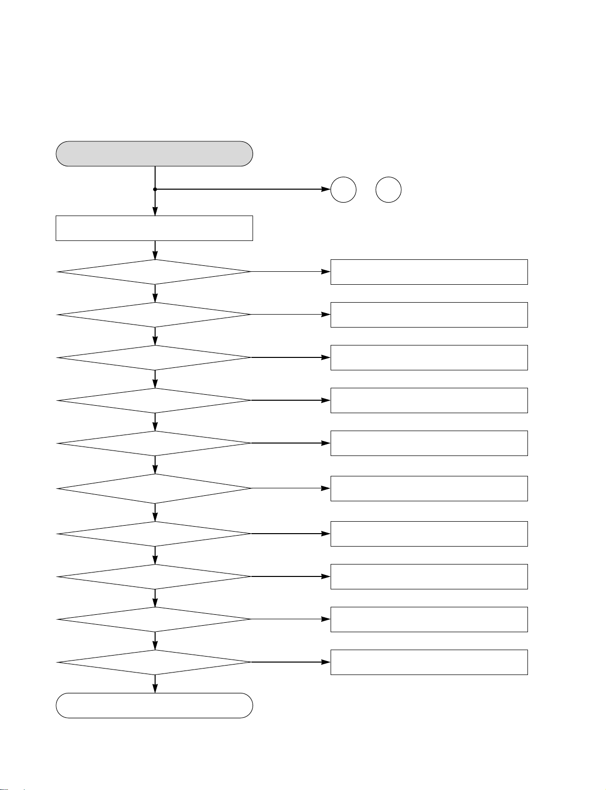
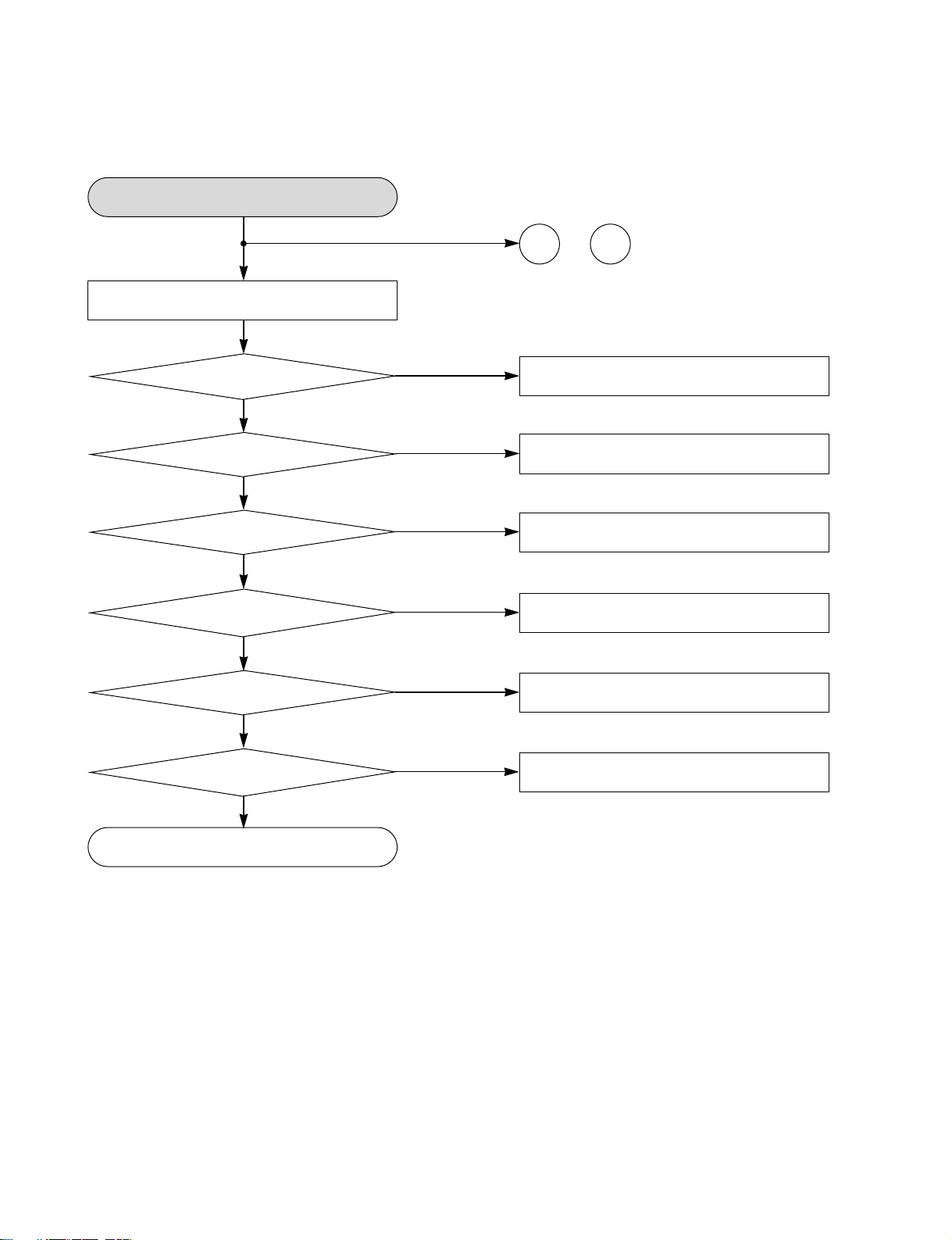
1. SYSTEM CONTROL ERROR CORRECTION FLOW CHART
Something wrong with
the system control?
No power?
YES
Checked the fuse?
YES
Checked the back up
Vdd and Gnd, Acc?
YES
Checked the main
Micom Back up, Vdd?
YES
Checked the main
Micom back up Gnd?
YES
Checked the main
Micom reset?
YES
NO
NO
NO
NO
NO
1-A
IC401(100, 99, 81, 30, 50, 47, 97, 20, 51)
1-F
~
Inside of CN801, F801(10A)
CN801(16, 15, 14)
IC301(15, 14)
IC402, IC401(90)
Checked the main
Micom X-tal?
YES
Checked the ACC in?
YES
Checked the
detachable switch?
YES
Checked the front
panel VDD?
YES
Checked the front
panel switch input?
YES
OK
Copyright © 2007 LG Electronics. Inc. All right reserved.
Only for training and service purposes
NO
NO
NO
NO
NO
2-1
X401, X402
F301, Q301, Q302, IC401(38), CN801(14)
CN901(19), IC401(74)
CN901(14), IC401(21), Q316, Q317
IC401(52, 53)
LGE Internal Use Only
Page 7
1-A
Not available to remocon?
YES
Checked the remocon
sens Vdd?
YES
Checked the remocon
sens line?
YES
OK
1-B
Not available to volume control?
YES
Checked the encoder volume?
NO
NO
NO
RMC1, R906
CN901(5), IC401(5)
EV901, CN901(6, 7), IC401(40, 41)
YES
Checked the volume
IC control?
YES
OK
1-C
Not available to key control?
YES
Checked the tact switch?
YES
Checked the key line?
YES
OK
NO
NO
NO
IC401(1, 2), IC601(22, 23)
SW901 ~ SW918, EV901
CN901(8, 9), IC401(52, 53)
LGE Internal Use Only
2-2
Copyright © 2007 LG Electronics. Inc. All right reserved.
Only for training and service purposes
Page 8
1-D
Not available to telephone mute?
YES
Checked the tel mute input?
YES
Checked the mute control?
YES
OK
1-E
Not available to ANT(Motor Type) control?
NO
NO
CN801(5), Q305,Q306, IC401(62)
IC401(1, 2, 3, 6, 61), IC601(21, 22,23),
IC801(22), Q707, Q708, Q709, Q710
YES
Checked the ANT
control?
YES
OK
1-F
Not available to remote(Power AMP) control?
YES
Checked the
remote control?
YES
OK
NO
NO
CN801(10), IC302(4), IC401(63)
CN801(6), IC301(12), IC401(87)
Copyright © 2007 LG Electronics. Inc. All right reserved.
Only for training and service purposes
2-3
LGE Internal Use Only
Page 9
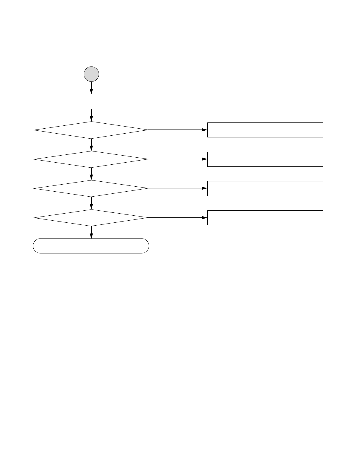
2. SOUND ERROR CORRECTION FLOW CHART
Something wrong with the sound?
No sounds of all functions?
YES
Checked the E-VR Vdd?
YES
Checked the E-VR Ground?
YES
Checked the E-VR control?
YES
Checked the E-VR
mute control?
YES
Checked the E-VR
signal in/out?
YES
NO
NO
NO
NO
NO
2-A
IC601(5, 6, 7, 8, 11, 13, 16, 17, 18, 19, 20)
2-F
~
IC601(24)
IC601(15)
IC601(22, 23), IC401(1, 2)
IC601(21), IC401(6)
Checked the power
Checked the power
Checked the power
Checked the main
LGE Internal Use Only
Checked the
power IC Vdd?
YES
IC Ground?
YES
IC Control?
YES
IC signal in/out?
YES
connector?
YES
OK
NO
NO
NO
NO
NO
2-4
IC801(6, 20)
IC801(1, 2, 8, 13, 18, 24)
IC801(4, 22), IC401(3, 10)
IC801(3, 5, 7, 9, 11, 12, 14, 15, 17, 19, 21, 23)
CN801(1, 2, 3, 4, 8, 9, 12, 13)
Copyright © 2007 LG Electronics. Inc. All right reserved.
Only for training and service purposes
Page 10
2-A
No REAR line out signal?
YES
Checked the line
out AMP Vdd?
YES
Checked the line out
AMP Vdd control?
YES
Checked the line
out AMP Ground?
YES
Checked the line out
AMP mute contorl?
YES
Checked the line out
AMP signal in/out?
YES
OK
NO
NO
NO
NO
NO
Q308, F303, IC701(8)
Q309, IC401(64)
IC701(4)
IC401(48), Q705, Q701, Q703
IC701(1, 2, 3, 5, 6, 7)
2-B
Hearing the Pop noise with TUNER function?
(RDS Model)
YES
Checked the
mute control?
YES
Checked the AF mute?
YES
OK
Copyright © 2007 LG Electronics. Inc. All right reserved.
Only for training and service purposes
NO
NO
2-5
IC401(1, 2, 3, 6, 61), IC601(21, 22,23),
IC801(22), Q707, Q708, Q709, Q710
TU101(19), IC401(4)
LGE Internal Use Only
Page 11

2-C
No subwoofer line out signal?
YES
Checked the line
out AMP Vdd?
YES
Checked the line out
AMP Vdd control?
YES
Checked the line
out AMP Ground?
YES
Checked the line out
AMP mute contorl?
YES
Checked the line out
AMP signal in/out?
YES
OK
NO
NO
NO
NO
NO
Q308, F303, IC702(8)
Q309, IC401(64)
IC702(4)
IC401(48), Q705, Q701, Q703
IC702(1, 2, 3, 5, 6, 7)
No output Beep sound?
LGE Internal Use Only
2-D
YES
Checked the
Beep control?
YES
OK
NO
2-6
IC401(80), BU302
Copyright © 2007 LG Electronics. Inc. All right reserved.
Only for training and service purposes
Page 12
2-E
No RSE line out signal?
YES
Checked the line
out AMP Vdd?
YES
Checked the line out
AMP Vdd control?
YES
Checked the line
out AMP Ground?
YES
Checked the line out
AMP mute contorl?
YES
Checked the line out
AMP signal in/out?
YES
OK
NO
NO
NO
NO
NO
Q308, F303, IC201(8)
Q309, IC401(64)
IC201(4)
IC401(11), Q201, Q202, Q203
IC201(1, 2, 3, 5, 6, 7)
2-F
Hearing the Pop noise with RSE function?
YES
Checked the
mute control?
YES
OK
Copyright © 2007 LG Electronics. Inc. All right reserved.
Only for training and service purposes
NO
2-7
IC401(11), Q201, Q202, Q203
LGE Internal Use Only
Page 13
CAUTION - Tip for repair
A
Before exchange power amp IC(TB2904) for no audio problem, you have to check
below list.
1. Check VCC (pin 20, 6) & GND
2. Check input pin 11, 12, 14, 15
3. Check Standby, pin 4
: Follow the below list.
4. Check Mute function, pin 22
: Follow the below list.
Stand-by Power Sound Voltage
ON OFF OFF 0 to 1.5
OFF ON ON 3.5 to 6V
5. Check Ripple pin 10.
: Normally it is high (about 10V)
Mute Sound Voltage
ON OFF 0 to 1.5
OFF ON 3.5 to 6V
6. Re-soldering all the pin of IC.
: Prevent crack of solder line.
* Keep changed IC, We request that you send it to HQ.
C1
C1
C6
C1
C1
PRE-GND
1 20 6
TAB V
IN1
11
IN2
12
C-GND
16
IN3
15
IN4
14
13
STBYRIP
10 25 22
2
C
4
CC1VCC2
OFF-SET
DET
OUT1
()
PW-GND1
OUT1 ( )
OUT2 ( )
PW-GND2
OUT2 ( )
OUT3 ( )
PW-GND3
OUT3 ( )
OUT4 ( )
PW-GND4
OUT4 ( )
MUTE
4
C
3
5
C
C
+
9
8
7
+
5
2
3
+
17
18
-
19
+
21
24
-
23
R
1
R
L
R
L
R
L
R
L
5 V
PLAY
MUTE
: PRE-GND
: PW-GND
Picture 1) Power IC desc.
LGE Internal Use Only
2-8
Copyright © 2007 LG Electronics. Inc. All right reserved.
Only for training and service purposes
Page 14
3. DISPLAY ERROR CORRECTION FLOW CHART
Something wrong with the display?
No display or some display is broken?
YES
Checked the LCD
driver Vdd?
YES
Checked the LCD
driver Ground?
YES
Checked the LCD
driver reset?
YES
Checked the LCD
driver OSC?
YES
Checked the LCD
driver data interface?
NO
NO
NO
NO
NO
3-A
3-C
~
IC901(56)
IC901(60)
IC901(57), CN901(11), IC401(75)
IC901(61)
IC401(76, 78, 79), CN901(3, 4, 10),
IC901(62, 63, 64)
YES
Checked the LCD
to LCD driver line?
YES
OK
Copyright © 2007 LG Electronics. Inc. All right reserved.
Only for training and service purposes
NO
2-9
IC901(1 ~ 55), LCD
LGE Internal Use Only
Page 15
3-A
Not available to illumination with button?
YES
Checked the dimmer
control input?
YES
Checked the LED Vdd?
YES
Checked the LED?
YES
OK
3-B
Don't moved level dancing bar?
YES
NO
NO
NO
F302, CN801(11), IC401(66), IC301(9)
IC301(4), CN901(13)
LD901 ~ LD923
Checked the level
meter signal Input?
LGE Internal Use Only
OK
YES
NO
2-10
IC601(25, 26), IC401(9, 54)
Copyright © 2007 LG Electronics. Inc. All right reserved.
Only for training and service purposes
Page 16
3-C
Not avaliable to LCD lighting control?
YES
Checked the
dimmer control input?
YES
Checked the LCD Vdd?
YES
Checked the LCD
Vdd control?
YES
Checked the LED?
YES
OK
NO
NO
NO
NO
F302, CN801(11), IC401(66), IC301(9)
IC301(4), Q320, Q322, CN901(12)
IC401(58, 59), Q319, Q321
LD930 ~ LD931
Copyright © 2007 LG Electronics. Inc. All right reserved.
Only for training and service purposes
2-11
LGE Internal Use Only
Page 17
4. TUNER ERROR CORRECTION FLOW CHART
Something wrong with
the Tuner system?
Not available to Tuner?
YES
Checked the
Tuner Vdd?
YES
Checked the Tuner
Vdd control?
YES
Checked the Tuner
Ground?
YES
Checked the PLL data?
YES
Checked the RF
signal in?
NO
NO
NO
NO
NO
4-A
TU101(11, 12, 13, 14, 15), IC401(44, 45, 46,)
4-C
~
TU101(4, 16), Q307, IC301(10, 14)
IC401(39, 64), Q318, IC301(11)
TU101(3, 10, 17)
TU101(1, 2)
Checked the mute
control? (RDS Model)
LGE Internal Use Only
YES
YES
Checked the
SD level?
YES
OK
NO
NO
2-12
TU101(19), IC401(4)
TU101(6), IC401(69)
Copyright © 2007 LG Electronics. Inc. All right reserved.
Only for training and service purposes
Page 18
4-A
Tuner no sound?
YES
Checked the Tuner
signal out?
YES
Checked the mute?
(RDS model)
YES
Checked the EVR
& power AMP?
YES
OK
4-B
NO
NO
NO
TU101(8, 9), IC601(5, 6)
TU101(19), IC401(4)
See the sound error correction process.
Not available to RDS function?
YES
Checked the
RDS data?
YES
OK
4-C
only RDS model
Not available to AF?
YES
Checked the
SMETER level?
YES
Checked the
RDS data?
YES
NO
NO
NO
TU101(20, 21), IC401(65, 83)
TU101(7), IC401(55)
TU101(20, 21), IC401(65, 83)
OK
Copyright © 2007 LG Electronics. Inc. All right reserved.
Only for training and service purposes
2-13
LGE Internal Use Only
Page 19
5. AUX ERROR CORRECTION FLOW CHART
Something wrong with
the Tuner system?
AUX no sound?
YES
Checked the AUX
signal input?
YES
Checked the EVR
& power AMP?
YES
OK
NO
NO
JK901, CN503,
CN901(15,17), IC601(11, 13)
See the sound error correction process.
LGE Internal Use Only
2-14
Copyright © 2007 LG Electronics. Inc. All right reserved.
Only for training and service purposes
Page 20

6. DVD ERROR CORRECTION FLOW CHART
Something wrong with the DVD system?
Loading/Unloading?
YES
Checked the eject
key defect?
YES
Checked the loading
motor IC Vdd?
YES
Checked the Load/
Unload control?
YES
Checked the Load/
Unload SW?
YES
Checked the
MPEG Vdd?
YES
NO
NO
NO
NO
NO
6-A
6-E
~
See the system error correction
process with the key control.
IC1202(1, 6)
IC1202(7, 8, 2, 3)
See Figure 9, 11
CN1301(2, 4), SW1301, CN1202(13)
See Figure 10, 12
IC1301(VDD33, VDD12, +3VA)
See Figure 13
Checked the
MPEG Ground?
YES
Checked the
MPEG Reset?
YES
Checked the
MPEG X-tal?
YES
Checked the main
Micom data interface?
YES
Checked the main
Micom data interface?
YES
Checked the disc
in load switch?
YES
OK
NO
NO
NO
NO
NO
NO
IC1301 VSS (1, 23, 35, 46, 63, 81,
100, 171, 180, 198, 208, 220, 234, 245)
IC401(23), IC203(5, 6)
CN902(10) IC1301 NRST(101)
X1301(1, 3)
See Figure 14
IC401(84, 85, 86, 29), CN902(4, 5, 6, 7)
IC1301(84, 85, 86, 87)
CN902(4, 5, 6, 7), CN1601(4, 5, 6, 7)
See Figure 15
CN1301(2, 4)
Copyright © 2007 LG Electronics. Inc. All right reserved.
Only for training and service purposes
2-15
LGE Internal Use Only
Page 21

6-A
6-B
Front LCD :
"INIT" display?
YES
Checked the
Input voltage of
MPEG IC?
YES
Checked the
GND condition of
MPEG IC?
YES
Checked
the MPEG
Reset?
YES
Check
the MPEG
X-tal?
YES
NO
NO
IC1301(VDD33,
VDD12, +3VA)
See Figure 13
IC1301 VSS (1, 23,
35, 46, 63, 81, 100,
171, 180, 198, 208,
220, 234, 235)
NO
IC203(5, 6), CN902(10)
IC1301 NRST(101)
NO
See Figure 14
IC401(23),
X1301(1, 3)
No display
on monitor?
YES
Checked the
MPEG Video signal
out?
YES
Check the Video
Amplifier Vcc,
GND?
YES
Check the Video
Amplifier In,
Out?
YES
Check the Video
switching IC Vcc &
GND?
YES
NO
NO
NO
NO
IC1301(161)
IC1603(3, 5)
See Figure 30
IC1603(2, 4)
See Figure 30
IC403(6, 7, 8)
Checked the
main Micom data
interface?
YES
Checked the
main Micom data
interface?
YES
OK
LGE Internal Use Only
NO
NO
IC401(84, 85, 86, 29),
CN902(4, 5, 6, 7)
IC1301(84, 85, 86, 87)
CN902(4, 5, 6, 7)
CN1601(4, 5, 6, 7)
See Figure 15
2-16
Check
the Video switching
IC In, Out, mute
signal?
YES
Check the
RCA cable?
YES
OK
Copyright © 2007 LG Electronics. Inc. All right reserved.
NO
IC403(3, 4, 5)
See Figure 31, 32
NO
CN403(1,2)
Only for training and service purposes
Page 22

6-C
No reading &
"FILE CHECK"
display?
YES
YES
Checked the
limit SW?
YES
Checked the
motor DRV mute
control?
YES
Checked
the focus
control?
YES
Checked the
focus error level out.
(FE Mon)?
YES
Checked
the tracking
control?
YES
NO
NO
NO
NO
NO
CN1202(13),
IC1301(75)
See Figure 18
IC1201(18)
See Figure 19
IC1201(10)
See Figure 20
FMON0
See Figure 20
IC1201(9)
See Figure 21
No Spindle
motor operating?
YES
Checked the
spindle driver
IC Vdd?
YES
Checked the
spindle driver IC
VHALF?
YES
Checked the
spindle driver IC
GND?
YES
Checked the
A1, A2, A3 of the
driver IC?
YES
NO
NO
NO
NO
IC1201(22, 27,
35, 42, 43)
IC1201(4, 16)
IC1201(36, 38, 41)
IC1201(37, 39, 40)
See Figure 16
Checked the
tracking error level
out.(TE Mon)
NO
FMON1
See Figure 21
YES
Checked
the RF signal
out check?
NO
CN1101(17)
See Figure 22
YES
Checked
the sled motor
control?
NO
IC1201(1, 2, 3, 4)
See Figure 23, 24
YES
OK
Copyright © 2007 LG Electronics. Inc. All right reserved.
Only for training and service purposes
2-17
Checked
the hall Bias
signals?
YES
Checked
the spindle motor
control?
YES
OK
NO
NO
IC1201(27~33)
See Figure 17
IC1201(5)
LGE Internal Use Only
Page 23

6-D
6-E
DVD/CD no sound?
YES
Checked the
MPEG Audio DATA
out?
YES
Checked
the DAC Vcc,
Vdd, GND?
YES
Checked
the DAC signal
In/out?
YES
Checked the
DAC mute?
YES
NO
(172, 173, 174,175)
NO
NO
NO
IC1401(4, 5, 6, 9, 10)
See Figure 25
IC1401(1, 2, 3, 7, 8, 16)
See Figure 26, 27
IC1301(178),
IC1401(11, 12)
See Figure 28
IC1301
No display on
front monitor?
YES
Check the
parking brake
control?
YES
Checked
the MPEG Video
signal out?
YES
Check the
Video Amplifier
Vcc, GND?
YES
Check the
Video Amplifier
In, Out?
YES
NO
NO
NO
NO
CN403(4),
Q415, IC401(12)
IC1301(161)
IC1603(3, 5)
See Figure 30
IC1603(2, 4)
See Figure 30
Checked the
OP AMP Vdd,
GND?
YES
Checked the
OP AMP signal
in/out?
YES
Checked the
E-VR & Power
AMP?
YES
OK
LGE Internal Use Only
NO
NO
NO
IC1402(4, 8)
See Figure 29
IC1402(1, 2, 6, 7)
See Figure 29
See a sound error
correction process.
2-18
Check the
Video switching IC
Vcc & GND?
NO
IC403(6, 7, 8)
See Figure 31
YES
Check the
Video switching
IC In, Out, mute
signal?
NO
IC403(3, 10, 11)
See Figure 31, 32
YES
Check the
front video signal
path?
NO
CN901(18)
YES
Check the
front video out
Jack?
NO
JK901, external
connecto to monitor
video cable
YES
OK
Copyright © 2007 LG Electronics. Inc. All right reserved.
Only for training and service purposes
CN503(4)
Page 24

• WAVEFORMS
Figure 1 (Initial connecting the Main connector and supply of electric power)
Figure 2 (Power ON and started the front Micom control data)
CH1 X401
CH2 X402
CH3 IC401(10)
CH4 Back-Up 5V L403
CH1 CN401(2)
Figure 3 (Front Micom control data)
CH2 CN401(4)
CH3 CN401(5)
CH4 CN401(6)
CH1 CN401(2)
CH2 CN401(4)
CH3 CN401(5)
CH4 CN401(6)
Copyright © 2007 LG Electronics. Inc. All right reserved.
Only for training and service purposes
2-19
LGE Internal Use Only
Page 25

Figure 4 (The E-VR control data)
Figure 5 (The E-VR Level meter signal data, 1kHz)
CH1 IC601(12)
CH2 IC601(13)
CH1 IC601(14) SAIN
Figure 6 (The Tuner initial control)
CH2 IC601(16) SAOUT
CH1 TU101 CE1(15)
CH2 TU101 CLK(13)
CH3 TU101 DI(14)
CH4 TU101 DO(12)
LGE Internal Use Only
2-20
Copyright © 2007 LG Electronics. Inc. All right reserved.
Only for training and service purposes
Page 26

Figure 7 (The Tuner control data)
Figure 8 (The RDS data)
CH1 TU101 CE2(11)
CH2 TU101 CLK(13)
CH3 TU101 DI(14)
CH4 TU101 DO(12)
CH1 TU101 RDS CLK(20)
Figure 9 (Loading motor control about loading condition)
CH2 TU101 DATA(21)
CH1 IC1202(7)
CH2 IC1202(8)
CH3 IC1202(2)
CH4 IC1202(3)
Copyright © 2007 LG Electronics. Inc. All right reserved.
Only for training and service purposes
2-21
LGE Internal Use Only
Page 27

Figure 10 (Switch condition about loading)
Figure 11 (Loading motor control about unloading condition)
CH1 CN1301(2)
CH2 CN1301(4)
CH3 CN1202(12)
CH4 SW1301
CH1 IC1202(7)
CH2 IC1202(8)
Figure 12 (Switch condition about unloading)
CH3 IC1202(2)
CH4 IC1202(3)
CH1 CN1301(2)
CH2 CN1301(4)
CH3 CN1202(12)
CH4 SW1301
LGE Internal Use Only
2-22
Copyright © 2007 LG Electronics. Inc. All right reserved.
Only for training and service purposes
Page 28

Figure 13 (MPEG IC voltage condition when the battery & ACC start on)
Figure 14 (MPEG RESET when the battery & ACC start on)
CH1 IC1301(2,13,25,
36,48...)
CH2 IC1301(24,47,
103,167...)
CH3
IC1301(151,160,165)
CH4 IC1301(1,12,23,
35,46...)
CH1 L1604
CH2 CN1601(10)
Figure 15 (SPI Interface)
CH3 X1301(1,3)
CH1 CN1601(6)
CH2 CN1601(5)
CH3 CN1601(4)
CH4 CN1601(7)
Copyright © 2007 LG Electronics. Inc. All right reserved.
Only for training and service purposes
2-23
LGE Internal Use Only
Page 29

Figure 16 (Spindle motor driving signal SA1, SA2, SA3 when spindle motor is working)
CH1 IC1201(37)
CH2 IC1201(39)
CH3 IC1201(40)
Figure 17 (Hall sensor signal H1+, H2+, H3+ and SPD when spindle motor is working)
CH1 IC1201(6)
Figure 18 (Limit switch condition signal LDIN when disc in)
CH2 IC1201(27)
CH3 IC1201(29)
CH4 IC1201(31)
CH1 CN1202(13)
LGE Internal Use Only
2-24
Copyright © 2007 LG Electronics. Inc. All right reserved.
Only for training and service purposes
Page 30

Figure 19 (Motor driver mute signal STBY when spinup process)
Figure 20 (Focus driving out F+, F- and focus error FE when nominal state)
CH1 IC1201(18)
CH1 TP : FMON0
Figure 21 (Track driving out T+, T- and track error TE when nominal state)
CH2 CN1101(1)
CH3 CN1101(4)
CH1 TP:FMON1
CH2 CN1101(3)
CH3 CN1101(2)
Copyright © 2007 LG Electronics. Inc. All right reserved.
Only for training and service purposes
2-25
LGE Internal Use Only
Page 31

Figure 22 (RF Signal)
CH1 CN1101(17)
Figure 23 (Sled stepping motor driving signal SIN1, SIN2 when sled move to origin point)
CH1 IC1201(7)
CH2 IC1201(6)
LGE Internal Use Only
2-26
Copyright © 2007 LG Electronics. Inc. All right reserved.
Only for training and service purposes
Page 32

Figure 24 (Stepping motor phase signal A+, A-, B+, B- when sled move to origin point)
CH1 CN1201(2)
CH2 CN1201(3)
CH3 CN1201(1)
CH4 CN1201(4)
Figure 25 (Voltage condition about DAC IC)
Copyright © 2007 LG Electronics. Inc. All right reserved.
Only for training and service purposes
2-27
CH1 IC1401(5)
CH2 IC1401(6)
CH3 IC1401(10)
CH4 IC1401(4,9)
LGE Internal Use Only
Page 33

Figure 26 (DAC Control Signal / No DATA signal)
Figure 27 (DAC control signal / 1kHz sinewave)
CH1 IC1401(1)
CH2 IC1401(2)
CH3 IC1401(3)
CH4 IC1401(16)
CH1 IC1401(7)
Figure 28 (Audio mute / Track jump)
CH2 IC1401(8)
CH1 IC1401(2)
CH2 IC1401(8)
CH3 IC1401(11)
CH4 IC1301(178)
LGE Internal Use Only
2-28
Copyright © 2007 LG Electronics. Inc. All right reserved.
Only for training and service purposes
Page 34

Figure 29 (OPAMP / 1kHz sinewave)
Figure 30 (6dB Video amplifier)
CH1 IC1402(6)
CH2 IC1402(7)
CH3 IC1402(8)
CH4 IC1402(4)
CH1 IC1603(3)
CH2 IC1603(4)
Figure 31 (IC403 NJM2279M)
CH3 IC1603(2)
CH4 IC1603(5)
CH1 IC403(4)
CH2 IC403(3)
CH3 IC403(5)
Copyright © 2007 LG Electronics. Inc. All right reserved.
Only for training and service purposes
2-29
LGE Internal Use Only
Page 35

Figure 32 (IC403 NJM2279M / Mute ON)
CH1 IC403(4)
CH2 IC403(3)
CH3 IC403(5)
LGE Internal Use Only
2-30
Copyright © 2007 LG Electronics. Inc. All right reserved.
Only for training and service purposes
Page 36

INTERNAL BLOCK DIAGRAM OF ICs
1. IC301 (HA13173AH)
1-1. BLOCK DIAGRAM
CTL 1
11
1.5V
CTL 2
13
2.5V
CTL 3
9
3.5V
VB
+B
DBUP
8
Over voltage detect
BIAS
REF
V
TSD
15
14
C2
0.1uF
VBUP
CBUP
100uF
VDDOUT
C1
100uF
CFREG
10uF
DEXT1
DEXT2
CILM
0.1uF
QFREG
CTL 4
EXTOUT
CEXT
10uF
ILMOUT
FREG B
RFREG3
RFREG1
12
5
4
2
2.5V
2.5V
REF
V
3
FREG F
GND
CVDD
10uF
DSPOUT
7
CDSP
10uF
REF
V
1
TAB
GND
CDOUT
6
AUDIOOUT
10
CCD
0.1uF
CAUDIO
10uF
RFREG2
Copyright © 2007 LG Electronics. Inc. All right reserved.
Only for training and service purposes
2-31
LGE Internal Use Only
Page 37

1-2. PIN FUNCTION (Note1)
Pin No.
Pin name Function
Normal
operation
(Note2) (Note3) (Note3)
TSD On VB=24V VB=50V
1 GND Ground - - - -
2 FREG_B External Trs bass drive (Note4) On/Off On/Off Off Off
3 FREG_F FREG feedback terminal On/Off On/Off Off Off
4 ILMOUT 8.4V output for JLM/500mAmax On/Off Off Off Off
5 CTL4 FREG control terminal - - - -
6 CDOUT 8.0V output for CD/1.3Amax (Note4) On/Off Off Off Off
7 DSPOUT 3.3V output for DSP/250mAmax (Note4) On/Off Off Off Off
8VB Battery - - - -
9 CTL3 ILM control terminal - - - -
10 AUDIOOUT 8.4V output for AUDIO/500mAmax (Note4) On/Off Off Off Off
11 CTL1 DSP, CD, Audio control terminal - - - -
12 EXTOUT High side output/600mAmax (Note4) On/Off Off Off Off
13 CTL2 EXT control terminal - - - -
14 VDDOUT 5.7V output for micro controller (Note4) On On On Off
15 VBUP Back up - - - -
Note1. In the uper table. “On” means always On. “Off” means compulsory Off and “On/Off” means that it can control by control
terminal.
Note2. Thermal protection circuit
A built-in thermal protection circuit (TSD:Thermal shut down) prevents thermal damage to the IC. All outputs except
VDD(pin14) and FREG (pin2&3) are switched off when the circuit operates, revert to the original state when the
temperature drops to a certain level.
Note3. Overvoltage protection circuit
The overvoltage protection circuit (surge protector) turns off all outputs without Vdd, when VB voltage is more than
about 21V. And the overvoltage protection circuit (surge protector) turns off Vdd output with other all outputs, when
VB voltage is more than about 26V. When the overvoltage protection operates on VB>=18V condition, the stand by
current increases.
Note 4. Overcurrent protection circuit
FREG_B (pin2), ILMOUT (pin4), CDOUT (pin6), DSPOUT (pin7), AUDIOOUT (pin10), EXITOUT (pin12), VDDOUT
(pin14) output circuits are built-in overcurrent protection circuit based on the respective output current. These
overcurrent protection circuits limit the current with a curve shape of “7” in the voltage-current graph. This prevents IC
destruction due to overcurrent.
Protection function
LGE Internal Use Only
2-32
Copyright © 2007 LG Electronics. Inc. All right reserved.
Only for training and service purposes
Page 38

2. IC401 (uPD78F1164)
2-1. PIN CONFIGURATION
uPD78F1164
Copyright © 2007 LG Electronics. Inc. All right reserved.
Only for training and service purposes
2-33
LGE Internal Use Only
Page 39

2-2. PIN DESCRIPTION
Pin No
1 PEV_CLK O Clock for interface with volume controller(IC601 13pin)
2 PEV_DO O To volume controller, data output(IC601 12pin)
3 PPWR_MUTE O Power AMP. Direct Mute Control Output(IC801 27pin)
4PAF_MUTE O Tuner AFS Port for AF Mute(TU101 14pin)
5 PRMC I Remote controller input
6 PSOFT_MUTE O Volume I.C Direct volume mute signal output(IC601 15pin)
7 N.C. O Not to be used
8 N.C. O Not to be used
9 PEV_SACLK O volume I.C Spectrum Analyzer Clock output(IC601 16pin)
10 PSTANDBY O Power AMP. Standby Control Output(IC801 27pin)
11 PDUAL_MUTE O
12 PDVD_PICKUP_PWR O 1. DVD Pickup 5V control output
13 PHAND_BREAK I Hand Break signal inputOnly LAD4700
14 PDVD_POWER O DVD system Vdd control output(IC304 4pin)
15 PVIDEO_F_MUTE O
16 PVIDEO_R_MUTE O Rear Video Signal mute control output
17 PFAN O Fan control output(Q402)
18 N.C. O Not to be used
19 N.C. O Not to be used
20 EVss1 Connect to GND
21 PFRT_PWR O
Name I/O Description
RSE audio Mute Control Output(Q201)
Only LAD4700
DVD Vdd Control
2. DVD Motor 8V control output
Front Video Signal mute control output
Only LAD4700
Front 5V control output(Q313)
Power control output for front panel
22 N.C. O Not to be used
23 PDVD_RST O DVD MPEG reset control(IC203 5pin)
24 PZERO_MUTE I DVD/CD zero mute signal input
25 N.C. O Not to be used
26 N.C. O Not to be used
27 N.C. O Not to be used
28 N.C. O Not to be used
29 PDVD_CE O DVD MPEG CE control(IC203 2pin)
30 EVdd1 I Positive power supply (+5V)
31 PDVD33 O DVD MPEG 3.3V Vdd on/off control output(Q304)
32 POPT_IN0 I For diode option check, signal 1 or 2 input0
33 POPT_IN1 I For diode option check, signal 1 or 2 input1
34 POPT_IN2 I For diode option check, signal 1 or 2 input2
35 POPT_OUT0 O For diode option check, signal 1 output
36 POPT_OUT1 O For diode option check, signal 2 output
37 POPT_OUT2 O For diode option check, signal 3 output
LGE Internal Use Only
2-34
Copyright © 2007 LG Electronics. Inc. All right reserved.
Only for training and service purposes
Page 40

Pin No
TUNER BAND OPTION
D401 D402 D403 AREA STEP
XXXOIRT/RE50K/9K
100K < - > 50K
10K <- > 9K
OXX ASIA/RC 100K/9K
OOXEUROPE/EW5/ RI 50K/ 9K
XXOEUROPE(LW)
XOO USA
D404 O RDS SEEK PI
D405 O LAD4710 DISPLAY
D406 O RDS ON
D407 O LAD4750 DISPLAY
XO
XL
LATIN/RD
Name I/O Description
38 PACC I ACC Control Input(Q301)
39 PAUDIO_PWR O Regulator Audio(Tuner and E-VR) 8.4V ON Control Output(IC301 11pin)
40 PVOLA O Volume rotary encoder A terminal signal input
41 PVOLB O Volume rotary encoder B terminal signal input
42 PBAT_CHK I Backup level detect input
43 N.C. I Not to be used
44 PPLL_DO O To PLL IC, data input(TU101 12pin)
45 PPLL_DI I From PLL IC, data output(TU101 14pin)
46 PPLL_CLK O Clock output for interface with PLL IC(TU101 13pin)
47 Avref I Reference voltage applied to D/A converter
48 PLINE_MUTE O LINE-OUT MUTE ON/OFF Control(Q705)
49 RTPD I
Wired remocon H/L selection input
Only LAD4750
50 Avref0 I Reference voltage applied to D/A converter
51 Avss - GND
52 PKEY1 I Key 1st line signal input
53 PKEY2 I Key 2nd line signal input
54 PLVL_METER I Volume I.C Spectrum Analyzer Analog Level Input(IC601 14pin)
55 PS_MTR I Radio station's strength signal input(TU101 7pin)
56 PQUALTY I Radio station's strength signal input(TU101 18pin)
57 RTPA I
58 PLIGHT O Front LCD back light On/Off Control Output(Q319)
59 PDIMMER O Dimmer Control output for LCD back light
Wired Remocon RTPA Key Input.
Only LAD4750
60 PAUX_MUTE O AUX mute control output, Only Option
61 PAUDIO_MUTE O System Audio Mute Control Output(Q706)
62 PTEL_MUTE O Tuner Signal Out Mute Control(Q305)
63 PANT O Antenna control output(IC302 1pin)
Copyright © 2007 LG Electronics. Inc. All right reserved.
Only for training and service purposes
2-35
LGE Internal Use Only
Page 41

Pin No
Name I/O Description
Power on control
64 PPWR O
1. Line out B+ on/off control(Q309)
2. Illumination On/off control(IC301 9Pin)
3. Tuner 5V control control(Q318)
65 PRDS_DI I From tuner pack, RDS data input(TU101 21Pin)
66 PDIM_IN I Dimmer input
67 PEEPROM_CE O CE1 Control with EEPROM Chip select(TU101 15Pin)
68 PPLL_CE O CE2 with PLL chip select(TU101 11Pin)
69 PPSD_ST I SD level & ST input from Tuner pack(TU101 5Pin)
70 PART_EN I ART Enable input, only Auto test equipment
71 PART_RX I Data input for ART, only Auto test equipment
72 PART_TX O Data output for ART, only Auto test equipment
73 N.C. O Not to be used
74 PFRT_DETECT I Front Panel detaching or attaching detect
75 PFRT_RST O Front LCD driver reset
76 PFRT_DO O Data output to Front LCD driver
77 PDISC_IN I Wake up signal input from DVD Mecha with Disc in
78 PFRT_CLK O CLK output to Front LCD driver
79 PFRT_CE I Data enable output to Front LCD driver
80 PBEEP O Buzzer output
81 PEXLVI I Low voltage detector(Connect to Vdd)
82 N.C. I Not to be used
83 PRDS_CLK I From tuner pack, RDS clock input(TU101 20Pin)
84 PDVD_DO O Data output for DVD
85 PDVD_DI I Data input of DVD
86 PDVD_CLK I CLK input of DVD
87 PREMOTE O External amp on(IC301 13Pin)
88 Download_CLK - CLK for Program upgrade
89 Download_IO - Data I/O for flash memory programmer(Pull-up register)
90 RESET - System reset input
91 SUB CLK I Sub clock 32.768 KHz
92 SUB CLK O Sub clock 32.768 KHz
93 FLMOD - Flash memory programming mode setting
94 MAIN CLK I X’tal 19.2 MHz
95 MAIN CLK O X’tal 19.2 MHz
96 REGC - Connect to VSS via a capacitor
97 Vss - Ground
98 Evss - Ground Potential for Ports
99 Vdd I Positive power supply (+5V)
100 Evdd I Positive power supply (+5V) For Ports
LGE Internal Use Only
2-36
Copyright © 2007 LG Electronics. Inc. All right reserved.
Only for training and service purposes
Page 42

3. IC403 (NJM2279M)
14 13 12 11 10
1
2
98
123456
7
PIN FUNCTION
1. Vin3
2. SW1
3. Vin2
4. MUTE2
5. Vout2
6. GND2
7. GND1
8. V
+
9. N. C.
10. Vout1
11. MUTE1
12. Vin1
13. SW2
14. V
-
3-1. PIN CONFIGURATION
3-2. BLOCK DIAGRAM
Copyright © 2007 LG Electronics. Inc. All right reserved.
Only for training and service purposes
2-37
LGE Internal Use Only
Page 43

4. IC601 (TDA7419)
ACOUTR/AC2OUTR
ACINR/FILOR
ACINL/FILOL
ACOUTL/AC2OUTL
SE3L/ACINL
SE2L
SE3R/ACINR
SE2R
SE1L OUTLF
MUTE
SCL
VDD
SDA
SAIN
SAOUT
VREF
MIX/OUTSW/OUTRR21
3
2
4
5
6
7
8
9
26
25
24
23
22
20
21
19
27
10
28
SE1R OUTLR
D04AU1569
DIFFL
DIFFG
DIFFR OUTSW/OUTLR2
OUTRF
OUTRR11
12
13
18
16
17
1514CREF GND
OUTLF
OUTRF
OUTLR
OUTRR
INPUT
MULTIPLEXE
R
InGain
AutoZero
I2C BUSDIGITAL CONTROL
OUTSW/
OUTLR2
MUTE
Loudness MiddleTreble BassSoftMute
Softstep
Volume
Softstep
MonoFader
Softstep
MonoFader
Softstep
MonoFader
SUPPLY
VDD CREFGND
SDASCL
DIFFG
DIFFL
SE1R
SE1L
DIFFR
SE2L
SE2R
Spectrum
Analyzer
Softstep
MonoFader
Subwoofer
LPF
Mix
Mix
MIX/
OUTSW/
OU
TRR2
HPF
HPF
Softstep
MonoFader
Softstep
MonoFader
AC2INL/
SE3L
AC2INR/
SE3R
ACOUTL/
AC2OUTL
ACOUT R/
AC2OUTR
ACINL/
FILOL
ACINR/
FILOR
VREFOUTF
SAOUT SAC LK
InGain
OUTLF
OUTRF
OUTLR
OUTRR
INPUT
MULTIPLEXER
InGain
AutoZero
I2C BUSDIGITAL CONTROL I2C BUSDIGITAL CONTROL
OUTSW/
OUTLR2
MUTE
Loudness MiddleTreble BassSoftMute
Softstep
Volume
Softstep
MonoFader
Softstep
MonoFader
Softstep
MonoFader
SUPPLY
VDD CREFGND
SDASCL
DIFFG
DIFFL
SE1R
SE1L
DIFFR
SE2L
SE2R
Spectrum
Analyzer
Softstep
MonoFader
Subwoofer
LPF
Mix
Mix
MIX/
OUTSW/
OU
TRR2
HPF
HPF
Softstep
MonoFader
Softstep
MonoFader
AC2INL/
SE3L
AC2INR/
SE3R
ACOUTL/
AC2OUTL
ACOUT R/
AC2OUTR
ACINL/
FILOL
ACINR/
FILOR
VREFOUTF
SAOUT SAC LK
InGain
4-1. PIN CONFIGURATION
4-2. BLOCK DIAGRAM
LGE Internal Use Only
2-38
Copyright © 2007 LG Electronics. Inc. All right reserved.
Only for training and service purposes
Page 44

4-3. PIN DESCRIPTION
Pin
N#
Pin Name Function I/O
1ACOUTR / AC2OUTR AC coupling right output / HPF filter AC2OUT right channel O
2ACINR / FILOR AC coupling right input / HPFfilter FILO right channel I/O
3ACINL / FILOL AC coupling left input / HPF filter FILO left channel I/O
4ACOUTL / AC2OUTL AC coupling left output / HPF filter AC2OUT left channel O
5SE3L / ACINL Single-ended input 3 left channel / AC coupling left input I
6 SE3R / ACINR Single-ended input 3 right channel / AC coupling right input I
7SE2LSingle-ended input 2 left channel I
8SE2RSingle-ended input 2 right channel I
9SE1LSingle-ended input 1 left channel I
10 SE1R Single-ended input 1 Right channel I
11 DIFFL Pseudo differential stereo input left I
12 DIFFG Pseudo differential stereo input common I
13 DIFFR Pseudo differential stereo input right I
14 CREF Reference capacitor O
15 GND Ground S
16 OUTSW / OUTLR2
Subwoofer output / 2
nd
rear left output
O
17 OUTRF Front right output O
18 OUTRR Rear right output O
19 OUTLR Rear left output O
20 OUTLF Front left output O
21 MUTE External mute pin I
22 SCL I2C bus clock I
23 SDA I2C bus data I/O
24 VDD Supply S
25 SAIN Spectrum analyzer clock input I
26 SAOUT Spectrum analyzer output O
27 VREF Vref output O
28 MIX / OUTSW / OUTRR2
Mix input / Additional subwoofer output / 2
nd
rear right output
I/O
Copyright © 2007 LG Electronics. Inc. All right reserved.
Only for training and service purposes
2-39
LGE Internal Use Only
Page 45

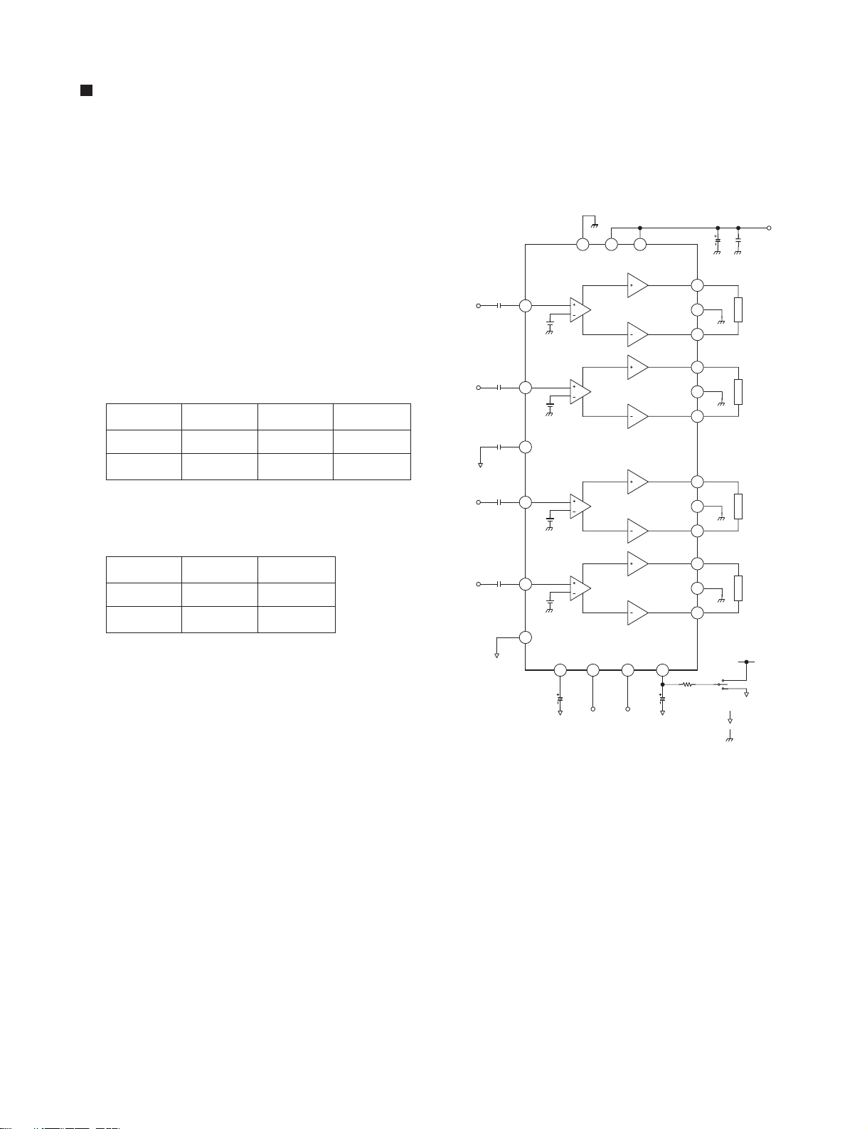
5. IC801 (TB2904HQ)
A
5-1. BLOCK DIAGRAM
C1
C1
C6
C1
C1
PRE-GND
1 20 6
TAB V
IN1
11
IN2
12
C-GND
16
IN3
15
IN4
14
13
STBYRIP
10 25 22
2
C
4
CC1VCC2
OFF-SET
DET
OUT1
()
PW-GND1
OUT1 ( )
OUT2 ( )
PW-GND2
OUT2 ( )
OUT3 ( )
PW-GND3
OUT3 ( )
OUT4 ( )
PW-GND4
OUT4 ( )
MUTE
4
C
3
5
C
C
+
9
R
8
7
+
5
2
3
+
17
18
-
19
+
21
24
-
23
R
1
L
R
L
R
L
R
L
5 V
PLAY
MUTE
: PRE-GND
: PW-GND
6. IC901 (PT6523)
6-1. PIN CONFIGURATION
SG49
SG50
SG51
SG52
COM1
COM2
COM3
VDD
INH
VDD1
VDD2
VSS
OSC
CE
CLK
DI
SG45
SG46
SG47
SG48
8
46
47
45
4
49
50
51
52
53
54
55
56
57
58
59
60
61
62
63
64 SG17
123456789
SG1
SG3
SG4
SG2
SG42
SG40
SG41
SG43
SG44
43
42
44
SG5
SG6
SG7
SG8
SG37
SG38
SG39
3934403541
SG9
SG36
38
36
37
10111213141516
SG11
SG12
SG10
SG13
SG33
SG34
SG35
33
32
SG32
31
SG31
30
SG30
29
SG29
SG28
28
27
SG27
26
SG26
SG25
25
24
SG24
SG23
23
22
SG22
21
SG21
20
SG20
SG19
19
18
SG18
17
SG14
SG15
SG16
LGE Internal Use Only
2-40
Copyright © 2007 LG Electronics. Inc. All right reserved.
Only for training and service purposes
Page 46

7. IC1502 (ES29LV320E)
7-1. PIN CONFIGURATION
A15
A14
A13
A12
A11
A10
A9
A8
A19
A20
WE#
RESET#
NC
WP#/ACC
RY/BY #
A18
A17
A7
A6
A5
A4
A3
A2
A1
1
2
3
4
5
6
7
8
9
10
11
12
13
14
15
16
17
18
19
20
21
22
23
24
7-2. BLOCK DIAGRAM
Vcc
Vss
Vcc Dete
ctor
RY/BY
48-Pin Standard TSOP
ES29LV320E
#
Timer/
Counter
48
47
46
45
44
43
42
41
40
39
38
37
36
35
34
33
32
31
30
29
28
27
26
25
DQ0-DQ15(A-1
A16
BYTE#
Vss
DQ15/A-1
DQ7
DQ14
DQ6
DQ13
DQ5
DQ12
DQ4
Vcc
DQ11
DQ3
DQ10
DQ2
DQ9
DQ1
DQ8
DQ0
OE#
Vss
CE#
A0
)
WE
RESET#
A<0:20
CE#
OE#
BYTE#
Analog Bias
Generato
#
Command
r
Registe
Write
State
Machin
e
r
Input/Output
Buff
ers
Data Latch/
Sector Swit
ches
Y-D ecode
Sense Amp
r
Y-D ecode
s
r
>
Ce
Chip Enable
Output Enable
c
Logi
X-Deco
Address Latch
der
ll Array
Copyright © 2007 LG Electronics. Inc. All right reserved.
Only for training and service purposes
2-41
LGE Internal Use Only
Page 47

7-3. PIN DESCRIPTION
Pin Description
A0-A20 21 Addresses
DQ0-DQ14 15 Data Inputs/Outputs
DQ15/A-1
CE# Chip Enable
OE# Output Enable
WE# Write Enable
WP#/ACC Hardware Write Protect/Acceleration Pin
RESET# Hardware Reset Pin, Active Low
BYTE# Selects 8-bit or 16-bit mode
RY/BY# Ready/Busy Output
Vcc
Vss Device Ground
NC Pin Not
DQ15 (Data Input/Output, Word Mode)
A-1 (LSB Address Input, Byte Mode)
3.0 volt-only single power supply
(see Product Selector Guide for speed options and voltage supply tolerances)
Connected Internally
LGE Internal Use Only
2-42
Copyright © 2007 LG Electronics. Inc. All right reserved.
Only for training and service purposes
Page 48

BLOCK DIAGRAMS
Copyright © 2007 LG Electronics. Inc. All right reserved.
Only for training and service purposes
LGE Internal Use Only
1. OVERALL BLOCK DIAGRAM
2-43 2-44
Page 49

2. DVD BLOCK DIAGRAM
Copyright © 2007 LG Electronics. Inc. All right reserved.
Only for training and service purposes
LGE Internal Use Only
2-45 2-46
Page 50

CIRCUIT DIAGRAMS
Copyright © 2007 LG Electronics. Inc. All right reserved.
Only for training and service purposes
LGE Internal Use Only
1. MAIN-1 CIRCUIT DIAGRAM
2-47 2-48
Page 51

2. MAIN-2 CIRCUIT DIAGRAM
Copyright © 2007 LG Electronics. Inc. All right reserved.
Only for training and service purposes
LGE Internal Use Only
2-49 2-50
Page 52

3. FRONT CIRCUIT DIAGRAM
Copyright © 2007 LG Electronics. Inc. All right reserved.
Only for training and service purposes
LGE Internal Use Only
• MODEL LAD4700(R)/4705(R)
2-51 2-52
Page 53

FRONT CIRCUIT DIAGRAM
Copyright © 2007 LG Electronics. Inc. All right reserved.
Only for training and service purposes
LGE Internal Use Only
• MODEL LAD4710(R)
2-53 2-54
Page 54

4. DVD-1 CIRCUIT DIAGRAM
Copyright © 2007 LG Electronics. Inc. All right reserved.
Only for training and service purposes
LGE Internal Use Only
2-55 2-56
Page 55

5. DVD-2 CIRCUIT DIAGRAM
Copyright © 2007 LG Electronics. Inc. All right reserved.
Only for training and service purposes
LGE Internal Use Only
2-57 2-58
Page 56

6. DVD-3 CIRCUIT DIAGRAM
Copyright © 2007 LG Electronics. Inc. All right reserved.
Only for training and service purposes
LGE Internal Use Only
2-59 2-60
Page 57

7. AUX CIRCUIT DIAGRAM 8. LCD LIGHTING CIRCUIT DIAGRAM
Copyright © 2007 LG Electronics. Inc. All right reserved.
Only for training and service purposes
LGE Internal Use Only
2-61 2-62
Page 58

PRINTED CIRCUIT BAORD DIAGRAMS
Copyright © 2007 LG Electronics. Inc. All right reserved.
Only for training and service purposes
LGE Internal Use Only
1. MAIN P.C.BOARD
(TOP VIEW) (BOTTOM VIEW)
2-63 2-64
Page 59

2. FRONT P.C.BOARD
Copyright © 2007 LG Electronics. Inc. All right reserved.
Only for training and service purposes
LGE Internal Use Only
• MODEL LAD4700(R)/4705(R)
(TOP VIEW)
(BOTTOM VIEW)
• MODEL LAD4710(R)
(TOP VIEW)
(BOTTOM VIEW)
2-65 2-66
Page 60

3. DVD P.C.BOARD
Copyright © 2007 LG Electronics. Inc. All right reserved.
Only for training and service purposes
LGE Internal Use Only
(TOP VIEW) (BOTTOM VIEW)
2-67 2-68
Page 61

4. AUX P.C.BOARD
Copyright © 2007 LG Electronics. Inc. All right reserved.
Only for training and service purposes
LGE Internal Use Only
MEMO
5. LCD LIGHTING P.C.BOARD
2-69 2-70
Page 62

SECTION 3 EXPLODED VIEWS
Copyright © 2007 LG Electronics. Inc. All right reserved.
Only for training and service purposes
LGE Internal Use Only
1. CABINET AND MAIN FRAME SECTION
276
270
288
273
A50
260
269
275
271
267
268
274
272
A45
262
261
266
A43
285
265
264
278
LCD1
284
280
263
A49
277
282
279
281
453
A44
451
451
295
451
CABLE2
A46
298
451
451
CABLE1
451
299
460
DVD
A41
451
A26
Accessory
Loc.No.
Loc.No.
Loc.No.
Loc.No.
801 808
818
836
Loc.No.
Loc.No.
Loc.No.
835
850
900
283
250
453
256
252
258
253
251
254
A42
255
257
294
454
451
291
MAIN
290
289
451
292
452
456
FAN1
293
296
455
297
451
452
451
3-1 3-2
Page 63

2. MECHANISM(PICK-UP) SECTION
Copyright © 2007 LG Electronics. Inc. All right reserved.
Only for training and service purposes
LGE Internal Use Only
MEMO
A03
3-3 3-4
 Loading...