

Page 1

Table Of Contents
1. INTRODUCTION.................................. 5
1.1 Purpose ...................................................... 5
1.2 Regulatory Information ............................... 5
2. PERFORMANCE ..................................7
2.1 System Overview.........................................7
2.2 Usable environment.....................................8
2.3 Radio Performance......................................8
2.4 Current Consumption.................................14
2.5 RSSI BAR ..................................................14
2.6 Battery BAR ...............................................15
2.7 Sound Pressure Level ...............................16
2.8 Charging ....................................................16
3. TECHNICAL BRIEF............................17
3.1 General Description ...................................17
3.2 GSM Mode.................................................19
3.3 UMTS Mode...............................................23
3.4 LO generation and distribution circuits ......25
3.5 Off-chip RF Components ...........................25
3.6 Digital Baseband(DBB/MSM7200) ............35
3.7 Hardware Architecture ...............................37
3.8. Subsystem(MSM7200) .............................39
3.9. Power Block..............................................42
3.10. External memory interface......................47
3.11. H/W Sub System ....................................49
3.12. Main Features.........................................76
4. TROUBLE SHOOTING.......................82
4.1 RF Component ..........................................82
4.2 SIGNAL PATH_UMTS RF .........................85
4.3 SIGNAL PATH_GSM RF ...........................86
4.4 Checking VCTCXO Block ..........................87
4.5 Checking Front-End Module Block ............89
4.6 Checking UMTS Block...............................91
4.7 Checking GSM Block.................................96
4.8 Checking Bluetooth Block........................102
4.9 Checking WLAN Block.............................104
4.10 Power ON Troubleshooting ...................108
4.11 Charger Troubleshooting .......................110
4.12 USB Troubleshooting.............................113
4.13 SIM Detect Troubleshooting ..................115
4.14 Camera Troubleshooting .......................117
4.15 Keypad Backlight Troubleshooting ........120
4.16 Main LCD Troubleshooting ....................121
4.17 Receiver Path ........................................122
4.18 Headset path .........................................124
4.19 Speaker phone path ..............................126
4.20 Main microphone ...................................128
4.21 Headset microphone..............................130
4.22 Vibrator ..................................................132
5. DOWNLOAD.....................................133
5.1 KS20 DOWNLOAD..................................133
6. BLOCK DIAGRAM ...........................146
6.1 GSM & UMTS RF Block ..........................146
6.2 Interface Diagram ....................................148
7. Circuit Diagram................................153
8. BGA IC PIN MAP..............................163
8. PCB LAYOUT ...................................169
9. Calibration & RF Auto Test
Program (Hot Kimchi) .....................177
9.1 Configuration of HOT KIMCHI .................177
9.2 How to use HOT KIMCHI.........................180
10. Phone Test Mode _ 3G smart
Phone KS20 ...................................182
11. EXPLODED VIEW & REPLACEMENT
PART LIST ..................................... 189
11.1 EXPLODED VIEW ................................ 189
11.2 Replacement Parts
<Mechanic component> ....................... 191
<Main component> ............................... 193
11.3 Accessory ............................................. 209
Copyright © 2007 LG Electronics. Inc. All right reserved.
Only for training and service purposes
- 3 -
LGE Internal Use Only
Page 2

- 4 -
LGE Internal Use Only
Copyright © 2007 LG Electronics. Inc. All right reserved.
Only for training and service purposes
Page 3

LGE Internal Use Only
Copyright © 2007 LG Electronics. Inc. All right reserved.
Only for training and service purposes
- 5 -
1.1 Purpose
This manual provides the information necessary to repair, calibration, description and download the
features of this model.
1.2 Regulatory Information
A. Security
Toll fraud, the unauthorized use of telecommunications system by an unauthorized part (for example,
persons other than your company’s employees, agents, subcontractors, or person working on your
company’s behalf) can result in substantial additional charges for your telecommunications services.
System users are responsible for the security of own system.
There are may be risks of toll fraud associated with your telecommunications system. System users
are responsible for programming and configuring the equipment to prevent unauthorized use. The
manufacturer does not warrant that this product is immune from the above case but will prevent
unauthorized use of commoncarrier telecommunication service of facilities accessed through or
connected to it. The manufacturer will not be responsible for any charges that result from such
unauthorized use.
B. Incidence of Harm
If a telephone company determines that the equipment provided to customer is faulty and possibly
causing harm or interruption in service to the telephone network, it should disconnect telephone
service until repair can be done. A telephone company may temporarily disconnect service as long as
repair is not done.
C. Changes in Service
A local telephone company may make changes in its communications facilities or procedure. If these
changes could reasonably be expected to affect the use of the phones or compatibility with the net
work, the telephone company is required to give advanced written notice to the user, allowing the user
to take appropriate steps to maintain telephone service.
D. Maintenance Limitations
Maintenance limitations on the phones must be performed only by the manufacturer or its authorized
agent. The user may not make any changes and/or repairs expect as specifically noted in this manual.
Therefore, note that unauthorized alternations or repair may affect the regulatory status of the system
and may void any remaining warranty.
1. INTRODUCTION
1. INTRODUCTION
Page 4

LGE Internal Use Only
Copyright © 2007 LG Electronics. Inc. All right reserved.
Only for training and service purposes
E. Notice of Radiated Emissions
This model complies with rules regarding radiation and radio frequency emission as defined by local
regulatory agencies. In accordance with these agencies, you may be required to provide information
such as the following to the end user.
F. Pictures
The pictures in this manual are for illustrative purposes only; your actual hardware may look slightly
different.
G. Interference and Attenuation
A phone may interfere with sensitive laboratory equipment, medical equipment, etc. Interference from
unsuppressed engines or electric motors may cause problems.
H. Electrostatic Sensitive Devices
ATTENTION
Boards, which contain Electrostatic Sensitive Device (ESD), are indicated by the sign.
Following information is ESD handling:
• Service personnel should ground themselves by using a wrist strap when exchange system boards.
• When repairs are made to a system board, they should spread the floor with anti-static mat which is
also grounded.
• Use a suitable, grounded soldering iron.
• Keep sensitive parts in these protective packages until these are used.
• When returning system boards or parts like EEPROM to the factory, use the protective package as
described.
1. INTRODUCTION
- 6 -
Page 5
LGE Internal Use Only
Copyright © 2007 LG Electronics. Inc. All right reserved.
Only for training and service purposes
2. PERFORMANCE
- 7 -
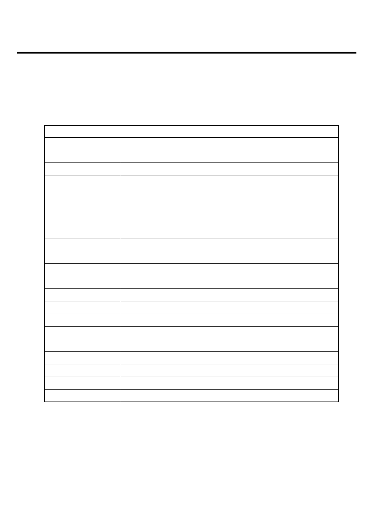
2.1 System Overview
2. PERFORMANCE
Item Specification
Shape GSM900/1800/1900 and WCDMA2100 - Bar type Handset
Size 99.8 X 58 X 12.9 mm
Weight Under 92.5g (with 1050mAh Battery)
Power 3.7 V normal, 1050 mAh Li-Polymer
Talk Time Over 100 min (WCDMA, Tx=-23 dBm, Voice)
(with 800mAh) Over 150 min (GSM, Tx=Level 5, Voice)
Standby Time Over 300 Hrs (WCDMA, DRX=1.28)
(with 800mAh) Over 400 Hrs (GSM, Paging period=9)
Antenna Internal type
LCD Main 2.8” 262K 240 X 320 pixel (TFT)
LCD Backlight White LED Back Light
Camera Auto Focus - 2.0 Mega pixel (CMOS) + VGA Video Call Camera
Vibrator Yes (Coin Type)
LED Indicator Yes
MIC Yes
Receiver Yes
Earphone Jack Yes (18 pin)
Connectivity Bluetooth, USB
Volume Key Push Type(+, -)
External Memory Yes
I/O Connect 18 Pin
Page 6

LGE Internal Use Only
Copyright © 2007 LG Electronics. Inc. All right reserved.
Only for training and service purposes
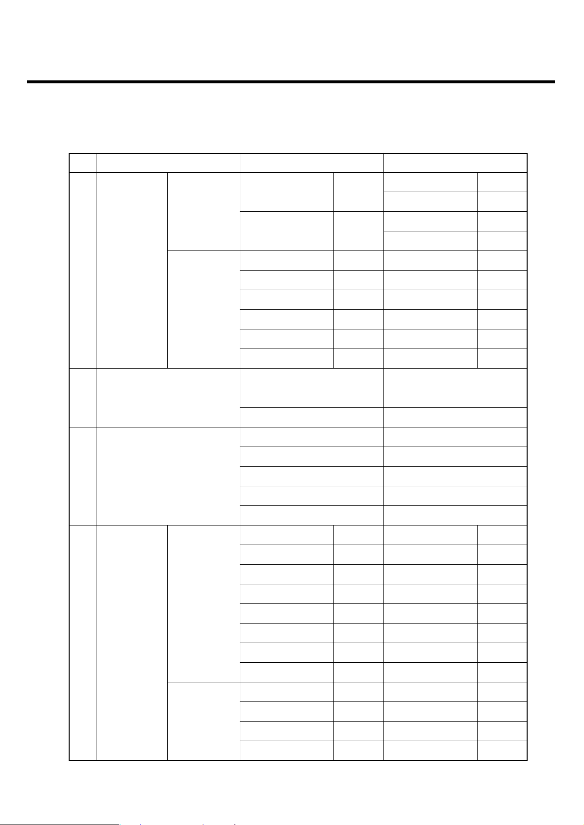
2.2 Usable environment
1) Environment
2) Environment (Accessory)
* CLA : 12 ~ 24 V(DC)
2.3 Radio Performance
1) Transmitter - GSM Mode
* In case of DCS : [A] -> 1710, [B] -> 1785 * In case of PCS : [A] -> 1850, [B] -> 1910
2. PERFORMANCE
- 8 -
Item Specification
Voltage 3.7 V(Typ), 3.2 V(Min), [Shut Down : 3.2 V]
Operation Temp -20 ~ +60°C
Storage Temp -20 ~ +70°C
Humidity 85 % (Max)
Reference Spec. Min Typ. Max Unit
TA Power Available power 100 220 240 Vac
No Item GSM DCS & PCS
100k~1GHz -39dBm
9k ~ 1GHz -39dBm
MS allocated 1G~[A]MHz -33dBm
Channel
1G~12.75GHz -33dBm
[A]M~[B]MHz -39dBm
Conducted [B]M~12.75GHz -33dBm
1 Spurious 100k~880MHz -60dBm 100k~880MHz -60dBm
Emission 880M~915MHz -62dBm 880M~915MHz -62dBm
Idle Mode
915M~1GHz -60dBm 915M~1GHz -60dBm
1G~[A]MHz -50dBm 1G~[A]MHz -50dBm
[A]M~[B]MHz -56dBm [A]M~[B]MHz -56dBm
[B]M~12.5GHz -50dBm [B]M~12.5GHz -50dBm
Page 7
LGE Internal Use Only
Copyright © 2007 LG Electronics. Inc. All right reserved.
Only for training and service purposes
2. PERFORMANCE
- 9 -
* In case of DCS : [A] -> 1710, [B] -> 1785 * In case of PCS : [A] -> 1850, [B] -> 1910
No Item GSM DCS & PCS
30M ~ 1GHz -36dBm
30M~1GHz -36dBm
MS allocated 1G~[A]MHz -30dBm
Channel
1G ~ 4GHz -30dBm
[A]M~[B]MHz -36dBm
Radiated [B]M~4GHz -30dBm
2Spurious 30M ~ 880MHz -57dBm 30M~880MHz -57dBm
Emission 880M ~ 915MHz -59dBm 880M~915MHz -59dBm
Idle Mode
915M~1GHz -57dBm 915M~1GHz -57dBm
1G~[A]MHz -47dBm 1G~[A]MHz -47dBm
[A]M~[B]MHz -53dBm [A]M~[B]MHz -53dBm
[B]M~4GHz -47dBm [B]M~4GHz -47dBm
3 Frequency Error ±0.1ppm ±0.1ppm
4 Phase Error
±5(RMS) ±5(RMS)
±20(PEAK) ±20(PEAK)
3dB below reference sensitivity 3dB below reference sensitivity
Frequency Error RA250 : ±200Hz RA250: ±250Hz
5 Under Multipath and HT100 : ±100Hz HT100: ±250Hz
Interference Condition TU50 : ±100Hz TU50: ±150Hz
TU3 : ±150Hz TU1.5: ±200Hz
0 ~ 100kHz +0.5dB 0 ~ 100kHz +0.5dB
200kHz -30dB 200kHz -30dB
250kHz -33dB 250kHz -33dB
Due to 400kHz -60dB 400kHz -60dB
Output RF
modulation 600 ~ 1800kHz -66dB 600 ~ 1800kHz -60dB
6 1800 ~ 3000kHz -69dB 1800 ~ 6000kHz -65dB
Spectrum
3000 ~ 6000kHz -71dB ≥6000kHz -73dB
≥6000kHz -77dB
Due to
400kHz -19dB 400kHz -22dB
Switching
600kHz -21dB 600kHz -24dB
transient
1200kHz -21dB 1200kHz -24dB
1800kHz -24dB 1800kHz -27dB
Page 8

LGE Internal Use Only
Copyright © 2007 LG Electronics. Inc. All right reserved.
Only for training and service purposes
2. PERFORMANCE
- 10 -
No Item GSM DCS & PCS
Frequency offset 800kHz
7 Intermodulation attenuation –
Intermodulation product should
be Less than 55dB below the
level of Wanted signal
Power control
Power Tolerance
Power control
Power Tolerance
Level (dBm) (dB) Level (dBm) (dB)
533±3 030±3
631±3 128±3
729±3 226±3
827±3 324±3
925±3 422±3
10 23 ±3 5 20 ±3
8 Transmitter Output Power 11 21 ±3 6 18 ±3
12 19 ±3 7 16 ±3
13 17 ±3 8 14 ±3
14 15 ±3 9 12 ±4
15 13 ±3 10 10 ±4
16 11 ±5 11 8 ±4
17 9 ±5 12 6 ±4
18 7 ±5 13 4 ±4
19 5 ±5 14 2 ±5
15 0 ±5
9 Burst timing Mask IN Mask IN
Page 9
LGE Internal Use Only
Copyright © 2007 LG Electronics. Inc. All right reserved.
Only for training and service purposes
2. PERFORMANCE
- 11 -
2) Transmitter - WCDMA Mode
No Item Specification
1 Maximum Output Power Class 3 : +24dBm(+1/-3dB)
2 Frequency Error ±0.1ppm
3 Open Loop Power control in uplink ±9dB@normal, ±12dB@extreme
Adjust output(TPC command)
cmd 1dB 2dB 3dB
+1 +0.5/1.5 +1/3 +1.5/4.5
4 Inner Loop Power control in uplink 0 -0.5/+0.5 -0.5/+0.5 -0.5/+0.5
-1 -0.5/-1.5 -1/-3 -1.5/-4.5
Group (10 equel command group)
+1 +8/+12 +16/+24
5 Minimum Output Power -50dBm(3.84MHz)
Qin/Qout : PCCH quality levels
6 Out-of-synchronization handling of output power Toff@DPCCH/Ior : -22 -> -28dB
Ton@DPCCH/Ior : -24 -> -18dB
7 Transmit OFF Power -56dBm(3.84MHz)
8 Transmit ON/OFF Time Mask
±25us
PRACH,CPCH,uplinlk compressed mode
±25us
9 Change of TFC
Power varies according to the data rate
DTX : DPCH off
(minimize interference between UE)
10 Power setting in uplink compressed ±3dB(after 14slots transmission gap)
11 Occupied Bandwidth(OBW) 5MHz(99%)
-35-15*(∆f-2.5)dBc@∆f=2.5~3.5MHz,30k
12 Spectrum emission Mask
-35-1*(∆f-3.5)dBc@∆f=3.5~7.5MHz,1M
-39-10*(∆f-7.5)dBc@∆f=7.5~8.5MHz,1M
-49dBc@∆f=8.5~12.5MHz,1M
Page 10

LGE Internal Use Only
Copyright © 2007 LG Electronics. Inc. All right reserved.
Only for training and service purposes
3)Receiver - GSM Mode
2. PERFORMANCE
- 12 -
No Item Specification
13 Adjacent Channel Leakage Ratio(ACLR)
33dB@5MHz, ACP>-50dBm
43dB@10MHz, ACP>-50dBm
-36dBm@f=9~150KHz, 1K BW
-36dBm@f=50KHz~30MHz, 10K BW
-36dBm@f=30MHz~1000MHz, 100K BW
14
Spurious Emissions -30dBm@f=1~12.5GHz, 1M BW
(*: additional requirement) (*)-41dBm@f=1893.5~1919.6MHz, 300K
(*)-67dBm@f=925~935MHz, 100K BW
(*)-79dBm@f=935~960MHz, 100K BW
(*)-71dBm@f=1805~1880MHz, 100K BW
15 Transmit Intermodulation
-31dBc@5MHz,Interferer -40dBc
-41dBc@10MHz, Interferer -40dBc
16 Error Vector Magnitude (EVM)
17.5%(>-20dBm)
(@12.2K, 1DPDCH+1DPCCH)
17 Transmit OFF Power
-15dB@SF=4.768Kbps, Multi-code
transmission
No Item GSM DCS & PCS
1
Sensitivity (TCH/FS Class II) -105dBm -105dBm
2
Co-Channel Rejection
C/Ic=7dB Storage -30 ~ +85
(TCH/FS Class II, RBER, TU high/FH)
3 Adjacent Channel 200kHz C/Ia1=-12dB C/Ia1=-12dB
Rejection 400kHz C/Ia2=-44dB C/Ia2=-44dB
Wanted Signal :-98dBm 1st Wanted Signal :-96dBm 1st
4
Intermodulation Rejection interferer:-44dBm 2nd interferer:-44dBm 2nd
interferer:-45dBm interferer:-44dBm
5
Blocking Response Wanted Signal :-101dBm Wanted Signal :-101dBm
(TCH/FS Class II, RBER)
Unwanted : Depend on Frequency Unwanted : Depend on Frequency
Page 11

LGE Internal Use Only
Copyright © 2007 LG Electronics. Inc. All right reserved.
Only for training and service purposes
2. PERFORMANCE
- 13 -
4) Receiver - WCDMA Mode
No Item Specification
1 Reference Sensitivity Level -106.7 dBm(3.84 MHz)
-25dBm(3.84MHz)
2 Maximum Input Level -44dBm/3.84MHz(DPCH_Ec)
UE@+20dBm output power(Class3)
3 Adjacent Channel Selectivity (ACS)
33dB
UE@+20dBm output power(Class3)
-56dBm/3.84MHz@10MHz
4In-band Blocking UE@+20dBm output power(Class3)
-44dBm/3.84MHz@15MHz
UE@+20dBm output power(Class3)
-44dBm/3.84MHz@f=2050~2095 and
2185~2230MHz
UE@+20dBm output power(Class3)
-30dBm/3.84MHz@f=2025~2050 and
5 Out-band Blocking 2230~2255MHz
UE@+20dBm output power(Class3)
-15dBm/3.84MHz@f=1~2025 and
2255~12500MHz
UE@+20dBm output power(Class3)
6 Spurious Response
-44dBm CW
UE@+20dBm output power(Class3)
-46dBm CW@10MHz
7 Intermodulation Characteristic -46dBm/3.84MHz@20MHz
UE@+20dBm output power(Class3)
-57dBm@f=9KHz~1GHz, 100K BW
8 Spurious Emissions -47dBm@f=1~12.5GHz, 1M BW
-60dBm@f=1920MHz~1980MHz, 3.84M BW
-60dBm@f=2110MHz~2170MHz, 3.84M BW
Page 12
LGE Internal Use Only
Copyright © 2007 LG Electronics. Inc. All right reserved.
Only for training and service purposes
2. PERFORMANCE
- 14 -
2.4 Current Consumption
1) KS20 Current Consumption
(Stand by and Voice Call Test Condition : Bluetooth off, LCD backlight off,Neighbor Cell off) (VT Test
Condition : Speaker off, LCD backlight On)
2) KS20 Current Consumption
(Stand by and Voice Call Test Condition : Bluetooth off, LCD backlight off,Neighbor Cell off) (VT Test
Condition : Speaker off, LCD backlight On)
2.5 RSSI BAR
Stand by Voice Call VT
WCDMA
Under 4.00 mA Under 600 mA Under 800mA
(DRX=1.28) (Tx=23dBm) (Tx=23dBm)
Under 3.00 mA Under 350 mA
GSM Paging=9 period (PCL=5)
Level Change WCDMA GSM
BAR 4 → 3 -82 ± 2 dBm -91 ± 2 dBm
BAR 3 → 2 -92 ± 2 dBm -96 ± 2 dBm
BAR 2 → 1 -102 ± 2 dBm -101 ± 2 dBm
BAR 1 → 0 -112 ± 2 dBm -106 ± 2 dBm
Stand by Voice Call VT
WCDMA
Under 2.5 mA Under 330 mA Under 500mA
(DRX=2.56) (Tx=10dBm) (Tx=10dBm)
Under 2.7 mA Under 270 mA
GSM
Paging=5 period (PCL=7)
Page 13
LGE Internal Use Only
Copyright © 2007 LG Electronics. Inc. All right reserved.
Only for training and service purposes
2.6 Battery BAR
2. PERFORMANCE
- 15 -
Indication Standby
Bar 4 100% ~ 76%
Bar 4 → 3 75%
Bar 3 → 2 50%
Bar 2 → 1 25%
Bar 1 → Empty 5%
Low Voltage, 10%
Warning message+ Blinking 5%
Power Off 3.20 ± 0.05V / 0%
Page 14
LGE Internal Use Only
Copyright © 2007 LG Electronics. Inc. All right reserved.
Only for training and service purposes
2. PERFORMANCE
- 16 -
2.7 Sound Pressure Level
2.8 Charging
• Charging Method : CC & CV (Constant Current and Constant Voltage)
• Maximum Charging Voltage : 4.2 V
• Maximum Charging Current : 900 mA
• Normal Battery Capacity : 1050 mAh
• Charging Time : Max 2.5 hours (except for trickle charging time)
• Full charging indication current (charging icon stop current) : 60 mA
• Cut-off voltage : 3.20 V
No Test Item Specification
1 Sending Loudness Rating (SLR) 8 ±3 dB
2 Receiving Loudness Rating (RLR)
Nor 2 ± 3 dB
Max -13 dB
3 Side Tone Masking Rating (STMR) Min 23 dB
4 Echo Loss (EL) Min 46 dB
5 Idle Noise-Sending (INS) Max -64 dBm0p
6 Idle Noise-Receiving (INR)
Nor
Under -54 dBPA
Max
7 Sending Loudness Rating (SLR) 8±3dB
8 Receiving Loudness Rating (RLR)
Nor -1 ±3 dB
Max -12 ±3 dB
9 Side Tone Masking Rating (STMR) Min 25 dB
10 Echo Loss (EL) Min 40 dB
11 Idle Noise-Sending (INS) Max -55 dBm0p
12 Idle Noise-Receiving (INR)
Nor Under -45 dBPA
Max Under -40 dBPA
TDMA Noise
-. GSM : Power Level : 5
DCS/PCS : Power Level : 0
(Cell Power : -90 ~ -105 dBm)
13
-. Acoustic (Max Vol.)
MS/Headset SLR : 8 ±3dB
MS/Headset RLR : -15 ± 3dB/-12
dB
(SLR/RLR : Mid-value setting)
MS
Headset
MS and
Headset
Max
Under -62 dBm
Page 15
LGE Internal Use Only
Copyright © 2007 LG Electronics. Inc. All right reserved.
Only for training and service purposes
3. TECHNICAL BRIEF
- 17 -
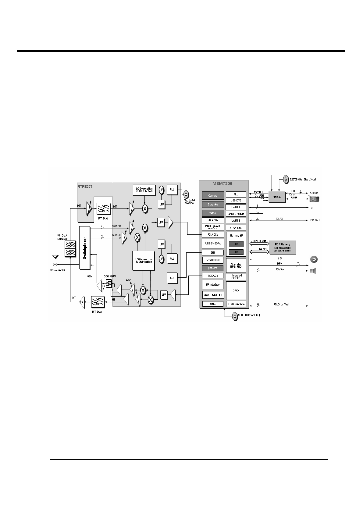
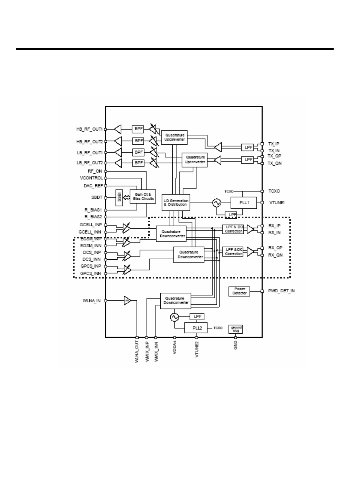
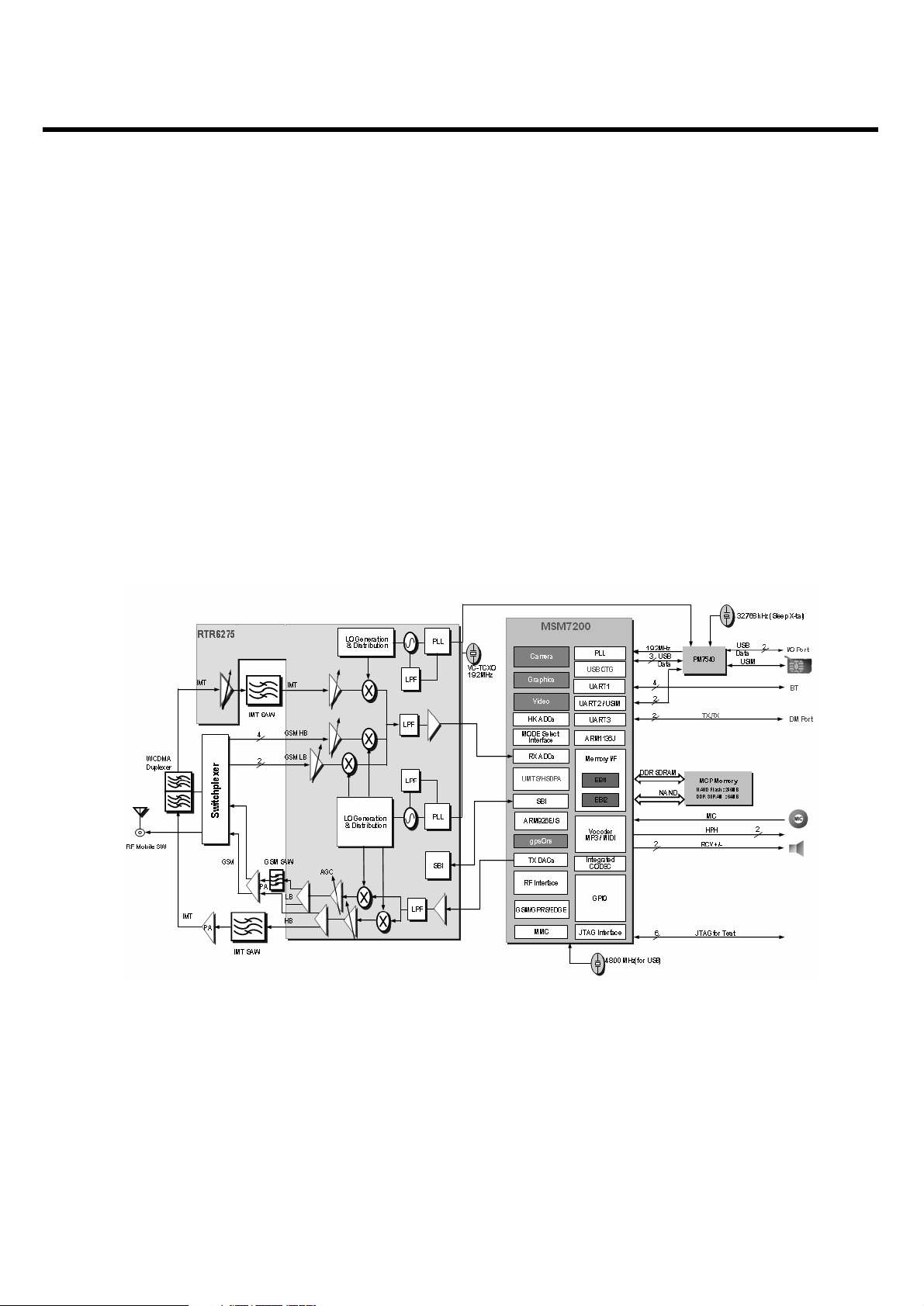
3.1 General Description
The KS20 supports UMTS-2100, GSM-900, DCS-1800, and PCS-1900 based
GSM/GPRS/EDGE/UMTS. All receivers and the UMTS transmitter use the radioOne1Zero-IF
architecture to eliminate intermediate frequencies, directly converting signals between RF
and baseband. The quad-band GSM transmitters use a baseband-to-IF upconversion followed by an
offset phase-locked loop that translates the GMSK-modulated or 8-PSK-modulated signal to RF.
1
QUALCOMM’s branded chipset that implements a Zero-IF radio architecture.
3. TECHNICAL BRIEF
[Fig 1.1] Block diagram of RF part
Page 16

LGE Internal Use Only
Copyright © 2007 LG Electronics. Inc. All right reserved.
Only for training and service purposes
A generic, high-level functional block diagram of KS20 is shown in Figure 1-1. One antenna collects
base station forward link signals and radiates handset reverse link signals. The antenna connects with
receive and transmit paths through a FEM(Front End Module).
The UMTS receive paths each include an LNA, an RF band-pass filter, and a downconverter that
translate the signal directly from RF-to-baseband using radioOne ZIF techniques. The RFIC’s Rx
analog baseband outputs, for the receive chains, connect to the MSM IC. The UMTS and GSM Rx
baseband outputs share the same inputs to the MSM IC.
For the transmit chains, the RTR6275 IC directly translates the Tx baseband signals (from the MSM
device) to an RF signal using an internal LO generated by integrated on-chip PLL and VCO. The
RTR6275 IC outputs deliver fairly high-level RF signals that are first filtered by Tx SAWs and then
amplified by their respective UMTS PAs. The high- and low-band UMTS RF transmit signals emerge
from the RTR6275 transceiver.
In the GSM receive path, the received RF signals are applied through their bandpass filters and downconverted directly to baseband in the RTR6275 transceiver IC.
These baseband outputs are shared with the UMTS receiver and routed to the MSM IC for further
signal processing.
The GSM/EDGE transmit path employs one stage of up-conversion and, in order to improve efficiency,
is divided into phase and amplitude components to produce an open-loop Polar topology:
1. The on-chip quadrature up-converter translates the GMSK-modulated signal or 8-PSK modulated
signal, to a constant envelope phase signal at RF;
2. The amplitude-modulated (AM) component is applied to the ramping control pin of Polar power
amplifier from a DAC within the MSM
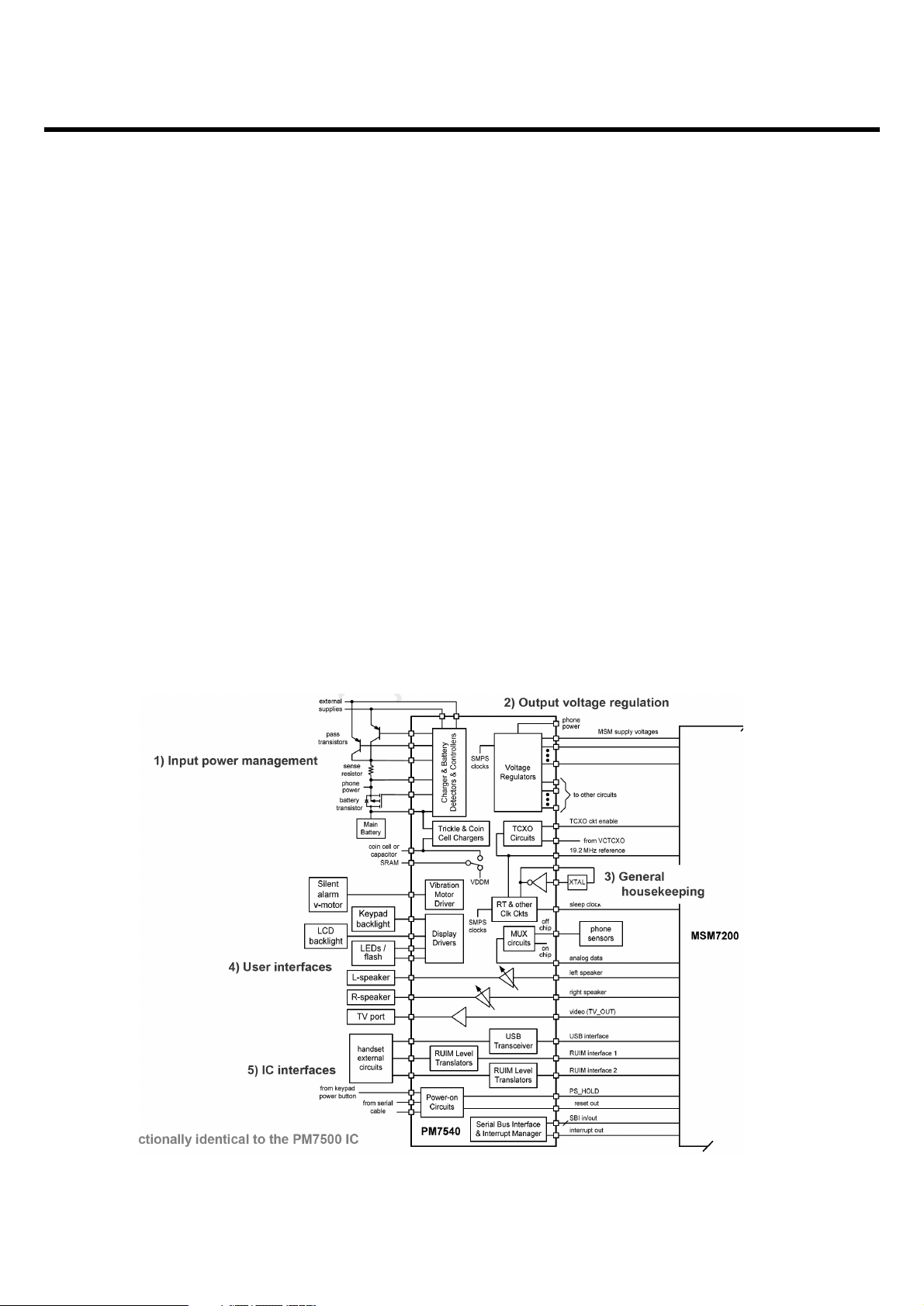
KS20 power supply voltages are managed and regulated by the PM7540 Power Management IC. This
versatile device integrates all wireless handset power management, general housekeeping, and user
interface support functions into a single mixed signal IC. It monitors and controls the external power
source and coordinates battery recharging while maintaining the handset supply voltages using low
dropout, programmable regulators.
The device’s general housekeeping functions include an ADC and analog multiplexer circuit for
monitoring on-chip voltage sources, charging status, and current flow, as well as user-defined off-chip
variables such as temperature, RF output power, and battery ID. Various oscillator, clock, and counter
circuits support IC and higher-level handset functions. Key parameters such as under-voltage lockout
and crystal oscillator signal presence are monitored to protect against detrimental conditions.
3. TECHNICAL BRIEF
- 18 -
Page 17
LGE Internal Use Only
Copyright © 2007 LG Electronics. Inc. All right reserved.
Only for training and service purposes
3. TECHNICAL BRIEF
- 19 -
3.2 GSM Mode
3.2.1 GSM Receiver
The Dual-mode KS20’s receiver functions are split between the three RFICs as follows:
• GSM-900, DCS-1800, and PCS-1900 UMTS-2100 modes bot use the RTR6275 IC only. Each mode
has independent front-end circuits and down-converters, but they share common baseband circuits
(with only one mode active at a time). All receiver control functions are beginning with SBI2-controlled
parameters.
RF Front end consists of antenna, antenna switch module(LSHS-M090U) which includes 3 RX saw
filters(GSM900, DCS and PCS). The antenna switch module allows multiple operating bands and
modes to share the same antenna. In KS20, a common antenna connects to one of six paths: 1)
UMTS-2100 Rx/Tx, 2) GSM-900 Rx, 3) GSM-900 Tx, 4) DCS-1800 Rx, and 5) DCS-1800, PCS-1900
Tx(High Band Tx’s share the same path), 6) PCS-1900 Rx. UMTS operation requires simultaneous
reception and transmission, so the UMTS Rx/Tx connection is routed to a duplexer that separates
receive and transmit signals. GSM900, DCS, and PCS operation is time division duplexed, so only the
receiver or transmitter is active at any time and a frequency duplexer is not required.
2
The RFIC operating modes and circuit parameters are MSM-controlled through the proprietary 3-line Serial Bus Interface (SBI). The Application
Programming Interface (API) is used to implement SBI commands. The API is documented in AMSS Software - please see applicable AMSS
Software documentation for details.
ANT_SEL0 ANT_SEL1 ANT_SEL2
GSM 850/GSM 900 TX HIGH HIGH LOW
GSM 1800/GSM 1900 TX HIGH LOW LOW
GSM 850 RX - - -
GSM 900 RX LOW LOW LOW
GSM 1800 RX LOW LOW LOW
GSM 1900 RX LOW LOW HIGH
WCDMA HIGH LOW HIGH
[Table 1.1] Antenna Switch Module Control logic
Page 18

LGE Internal Use Only
Copyright © 2007 LG Electronics. Inc. All right reserved.
Only for training and service purposes
The GSM900, DCS, and PCS receiver inputs of RTR6275 are connected directly to the transceiver
front-end circuits(filters and antenna switch module). GSM900, DCS, and PCS receiver inputs use
differential configurations to improve common-mode rejection and second-order non-linearity
performance. The balance between the complementary signals is critical and must be maintained from
the RF filter outputs all the way into the IC pins
Since GSM900, DCS, and PCS signals are time-division duplex (the handset can only receive or
transmit at one time), switches are used to separate Rx and Tx signals in place of frequency duplexers this is accomplished in the switch module.
The GSM900, DCS, and PCS receive signals are routed to the RTR6275 through band selection filters
and matching networks that transform single-ended 50-Ω sources to differential impedances optimized
for gain and noise figure. The RTR input uses a differential configuration to improve second-order intermodulation and common mode rejection performance. The RTR6275 input stages include
MSMcontrolled gain adjustments that maximize receiver dynamic range.
The amplifier outputs drive the RF ports of the quadrature RF-to-baseband downconverters. The
downconverted baseband outputs are multiplexed and routed to lowpass filters (one I and one Q)
having passband and stopband characteristics suitable for GMSK or 8-PSK processing. These filter
circuits include DC offset corrections. The filter outputs are buffered and passed on to the MSM7200 IC
for further processing (an interface shared with the RFR6275 UMTS receiver outputs
3. TECHNICAL BRIEF
- 20 -
Page 19
LGE Internal Use Only
Copyright © 2007 LG Electronics. Inc. All right reserved.
Only for training and service purposes
3. TECHNICAL BRIEF
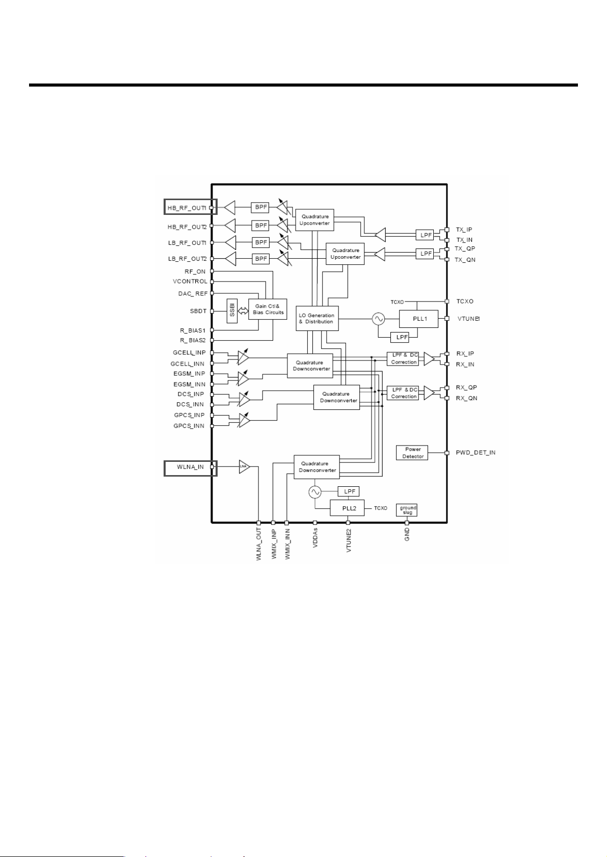
- 21 -
[Fig 1.2] RTR6275 RX feature
Page 20

LGE Internal Use Only
Copyright © 2007 LG Electronics. Inc. All right reserved.
Only for training and service purposes
3.2.2 GSM Transmitter
The RTR6275 transmitter outputs(DA_HB2_OUT and DA_LB1_OUT)include on-chip output matching
inductors. 50ohm output impedance is achieved by adding a series capacitor at the output pins. The
capacitor value may be optimized for specific applictions and PCB characteristics based on pass-band
symmetry about the band center frequency, the suggested starting value is shown in Figure1.2.
The RTR6275 IC is able to support GSM 900 and GSM 1800/1900 mode transmitting. This design
guideline shows a tri-band GSM application.
Both high-band and low band outputs are followed by resistive pads to ensure that the load Presented
to the outputs remains close to 50ohm. The low-band GSM. Tx path also includes a Tx-band SAW filter
to remove noise-spurious components and noise that would be amplified by the PA and appear in the
GSM Rx band
3. TECHNICAL BRIEF
- 22 -
[Fig 1.3] GSM Transmitter matching
18Ω
300Ω300Ω
18Ω
300Ω300Ω
Page 21

LGE Internal Use Only
Copyright © 2007 LG Electronics. Inc. All right reserved.
Only for training and service purposes
3. TECHNICAL BRIEF
- 23 -
3.3 UMTS Mode
3.3.1 Receiver
The UMTS duplexer receiver output is routed to LNA circuits within the RTR6275 device. The UMTS Rx
input is provided with an on-chip LNA that amplifies the signal before a second stage filter that provides
differential downconverter. This second stage input is configured differentially to optimize second-order
intermodulation and common mode rejection performance. The gain of the UMTS frontend amplifier and
the UMTS second stage differential amplifier are adjustable, under MSM control, to extend the dynamic
range of the receivers. The second stage UMTS Rx amplifiers drive the RF ports of the quadrature RFto-baseband downconverters. The downconverted UMTS Rx baseband outputs are routed to lowpass
filters having passband and stopband characteristics suitable for UMTS Rx processing. These filter
circuits allow DC offset corrections, and their differential outputs are buffered to interface shared with
GSM Rx to the MSM IC. The UMTS baseband outputs are turned off when the RTR6275 is
downconverting GSM signals and on when the UMTS is operating.
3.3.2 Transmitter
The UMTS Tx path begins with differential baseband signals (I and Q) from the MSM device.
These analog input signals are amplified, filtered, and applied to the quadrature upconverter mixers.
The up-converter output is amplified by multiple variable gain stages that provide transmit AGC control.
The AGC output is filtered and applied to the driver amplifier; this output stage includes an integrated
matching inductor that simplifies the external matching network to a single series capacitor to achieve
the desired 50-Ω interface.
The RTR6275 UMTS output is routed to its power amplifier through a bandpass filter, and delivers fairly
high-level signals that are filtered and applied to the PA. Transmit power is delivered from the duplexer
to the antenna through the switch module.
The transceiver LO synthesizer is contained within the RTR6275 IC with the exception of the off-chip
loop filter components and the VC-TCXO. This provides a simplified design for multimode applications.
The PLL circuits include a reference divider, phase detector, charge pump, feedback divider, and digital
logic generator.
UMTS Tx. Using only PLL1, the LO generation and distribution circuits create the necessary LO signals
for nine different frequency converters. The UMTS transmitter also employs the ZIF architecture to
translate the signal directly from baseband to RF.
This requires FLO to equal FRF, and the RTR6275 IC design achieves this without allowing FVCO to
equal FRF.
The RTR6275 IC is able to support UMTS 2100/1900 and UMTS 850 mode transmitting. This design
guideline shows only UMTS 2100 applications.
Page 22
LGE Internal Use Only
Copyright © 2007 LG Electronics. Inc. All right reserved.
Only for training and service purposes
3. TECHNICAL BRIEF
- 24 -
[Figure 1.4] RTR6275 IC functional block diagram
WCDMA_2100_TX
WCDMA_2100_RX
Page 23
LGE Internal Use Only
Copyright © 2007 LG Electronics. Inc. All right reserved.
Only for training and service purposes
3.4 LO generation and distribution circuits
The integrated LO generation and distribution circuits are driven by internal VCOs to support various
modes to yield highly flexible quadrature LO outputs that drive all GSM/EDGE and UMTS band
upconverters and downconverters; with the help of these LO generation and distribution circuits, true
zero-IF architecture is employed in all GSM and UMTS band receivers and transmitters to translate the
signal directly from RF to baseband and from baseband to RF.
Two fully functional fractional-N synthesizers, including VCOs and loop filters, are integrated within the
RTR6275 IC. The first synthesizer (PLL1) creates the transceiver LOs that support the UMTS
2100/1900/1800 transmitter, and all four GSM band receivers and transmitters including: GSM 850,
GSM 900, GSM 1800, and GSM 1900. The second synthesizer (PLL2) provides the LO for the UMTS
2100/1900/1800 receiver. An external TCXO input signal is required to provide the synthesizer
frequency reference to which the PLL is phase and frequency locked.
The RTR6275 IC integrates most of PLL loop filter components on-chip except two off-chip loop filter
series capacitors, and significantly reduces off-chip component requirement. With the integrated
fractional-N PLL synthesizers, the RTR6275 has the advantages of more flexible loop bandwidth
control, fast lock time, and low-integrated phase error
3.5 Off-chip RF Components
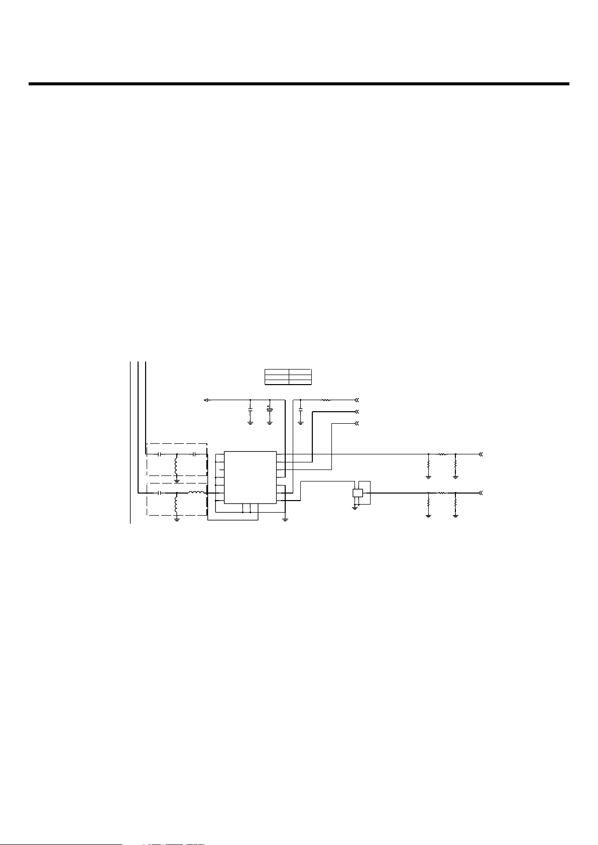
3.5.1 WCDMA PAM (U503: ACPM-7381)
The UMTS PA output power is monitored by l power detector circuits(U500 : RTR6275).
This detector voltage can be used for transmitter calibration and monitor to meet RF system
specification.
3. TECHNICAL BRIEF
- 25 -
[Figure 1.5] WCDMA PAM, Duplexer, Coupler
(1608)
10dB
SMPY0015501
As close as possible
20dB
C565
100p
1nH
L520
3p
C554
33p
C561
C560
33p
FL503
3
ANT
4
PGNDRX
1
2
TX
SDMY0001301
ACMD-7602
NA
C564
L522
4.7nH
100p
C557
C566
100p
L523
10nH
220p
C556
2.7nH
L521
L524
10nH
C559
33p
91
C553
33p
R520
VPWR
33p
C558
R521
91
C563
51
1.5p
R518
VMODE0
3
VMODE1
U503ACPM-7381
6
GND1
GND2
7
GND3
9
PGND
11
RFIN
2
8
RFOUT
VCC1
110
VCC2
VEN
5
4
10u
C555
EFCH1950TDF1
G12G2
3
G3
5
IN
1
O1
4
75
R519
FL504
U502
SCDY0003402
50OHM
4
3
COUP IN
2
OUT
1
PWR_DET
RX_WCDMA_2100
WCDMA_PA_ON
WCDMA_PA_R0
WCDMA_2100_TX_OUT
Page 24
LGE Internal Use Only
Copyright © 2007 LG Electronics. Inc. All right reserved.
Only for training and service purposes
3.5.2 VCTCXO (X500 : TG-5010LH (19.2M))
The Voltage Controlled Temperature Compensated Crystal Oscillator (VCTCXO) provides the
reference frequency for all RFIC synthesizers as well as clock generation functions within the
MSM7200 IC. The oscillator frequency is controlled by the MSM7200 IC.s TRK_LO_ADJ pulse density
modulated signal in the same manner as the transmit gain control TX_AGC_ADJ. A two-pole RC
lowpass filter is recommended on this control line.
The PM7540 IC controls the handset power-up sequence, including a special VCTCXO warm-up
interval before other circuits are turned on. This warm-up interval (as well as other TCXO controller
functions) is enabled by the MSM TCXO_EN line . The PM7540 IC VREG_TCXO regulated output
voltage is used to power the VCTCXO and is enabled before most other regulated outputs.
Any GSM mode power control circuits within the MSM7200 IC require a reference voltage for proper
operation and sufficient accuracy. Connecting the PM7540 IC REF_OUT directly to the MSM6275 IC
GSM_PA_PWR_CTL_REF provides this reference. This sensitive analog signal needs a 0.1 µF low
frequency filter near to MSM side, and isolate from digital logic and clock traces with ground on both
sides, plus ground above and below if routed on internal layers.
3.5.3 Front-End Module (FL500 : LSHS-M090UE)
switch module select the operating frequency and band. UMTS operation requires simultaneous
reception and transmission, so the UMTS Rx/Tx connection is routed to a duplexer that separates
receive and transmit signals. The active connection is MSM-selected by three control lines (GPIO[75],
GPIO[74], and GPIO[731]). These GPIOs are programmed to be ANT_SEL0, ANT_SEL1, and
ANT_SEL2) respectively.
3. TECHNICAL BRIEF
- 26 -
[Table 1.2] Front End Module control logic
ANT_SEL0 ANT_SEL1 ANT_SEL2
GSM 850/GSM 900 TX HIGH HIGH LOW
GSM 1800/GSM 1900 TX HIGH LOW LOW
GSM 850 RX - - -
GSM 900 RX LOW LOW LOW
GSM 1800 RX LOW LOW LOW
GSM 1900 RX LOW LOW HIGH
WCDMA HIGH LOW HIGH
Page 25

LGE Internal Use Only
Copyright © 2007 LG Electronics. Inc. All right reserved.
Only for training and service purposes
3. TECHNICAL BRIEF
- 27 -
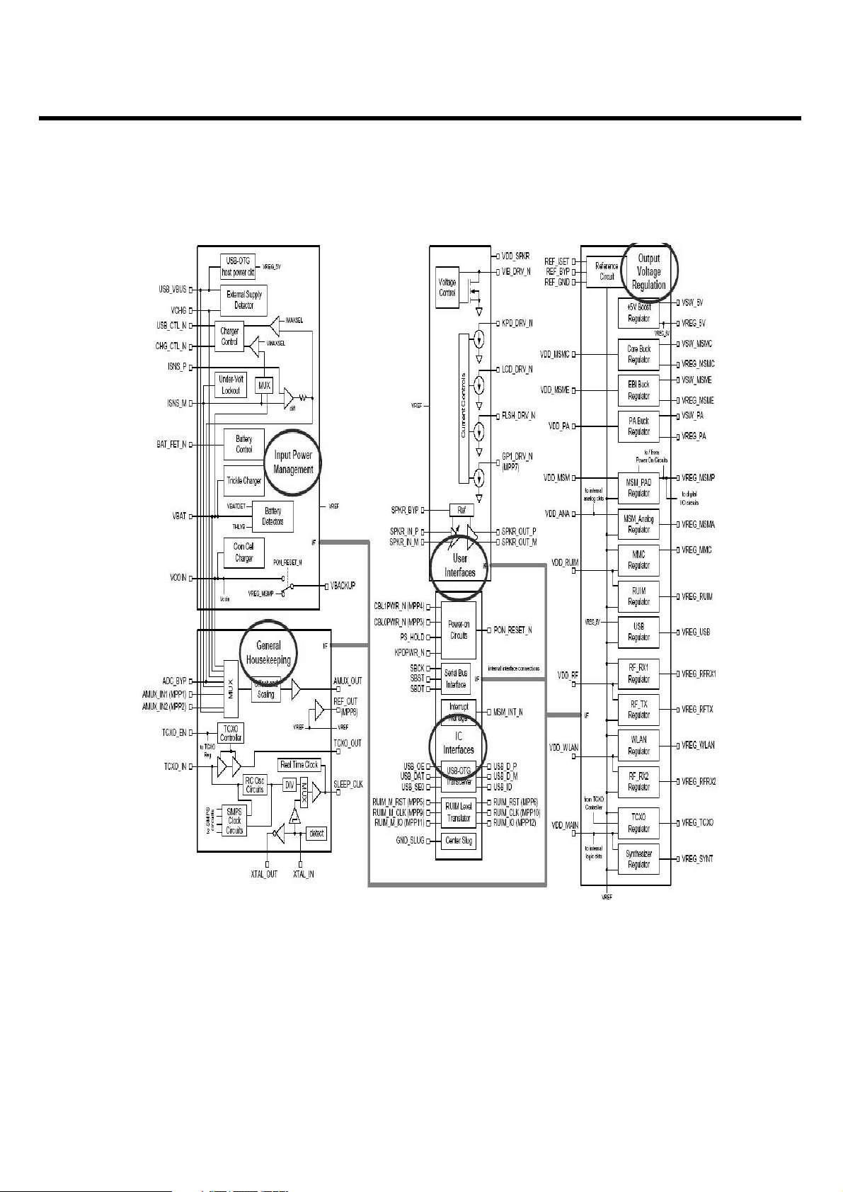
3.5.4 PMIC Functional Block Diagram (U304 : PM7540)
• Complete power management, housekeeping, and user interface functions for wireless devices (CDMA,
non-CDMA handsets, and PDAs)
• Input power management
- Valid external supply attachment and removal detection
- Supports unregulated (closed-loop) external charger supplies and USB supplies as input power sources
- Supports lithium-ion main batteries
- Trickle, constant current, constant voltage, and pulsed charging of the main battery
- Supports coin cell backup battery (including charging)
- Battery voltage detectors with programmable thresholds
- VDD collapse protection
- Charger current regulation and real-time monitoring for over-current protection
- Charger transistor protection by power limit control
- Control drivers for two external pass transistors and one external battery MOSFET (MOSFET is optional)
- Voltage, current, and power control loops
- Automated recovery from sudden momentary power loss
• Output voltage regulation
- One boost (step-up) switched-mode power supply (SMPS) for driving white LEDs and hosting USB-OTG
- Four buck (step-down), switched-mode power supplies for efficiently generating MSMC1, MSMC2,
MSME, and PA supply voltages
- Supports dynamic voltage scaling (DVS) for MSMC1, MSMC2, and PA outputs
- 18 low-dropout regulator circuits with programmable output voltages, implemented using three different
current ratings: 300 mA (four), 150 mA (ten), and 50 mA (four). These can be used to power MSMA,
MSMP, MSME2, MMC, RFRX1, RFRX2, RFTX, TCXO, SYNT, RUIM1, RUIM2, USB, WLAN, MDDI,
CAM, BT, AUX1, and AUX2 circuits.
- One MIC bias regulator circuit
- All regulators can be individually enabled/disabled for power savings
- Low power mode available on most regulators
- All regulated outputs are derived from a common bandgap reference (close tracking)
• Integrated handset-level housekeeping functions reduces external parts count, size, and cost
- Analog multiplexer selects from five internal and up to 28 external inputs
- Multiplexer output's offset and gain are adjusted, increasing the effective ADC resolution
- Adjusted multiplexer output is buffered and routed to an MSM device ADC
- Dual oscillators: a 32.768 kHz off-chip crystal and an on-chip RC assure MSM device sleep clock
- Crystal oscillator detector and automated switch-over upon lost oscillation
- Real-time clock for tracking time and generating associated alarms
- On-chip adjustments minimize crystal oscillator frequency errors
- Control TCXO warm-up and synchronize, deglitch, and buffer the TCXO signal
- TCXO buffer control for optimal QPH/catnap timing
- Multistage over temperature protection (smart thermal control)
• Integrated handset-level user interfaces
- Four programmable current sinks recommended as keypad backlight, LCD backlight, camera flash, and
general-purpose drivers
Page 26
LGE Internal Use Only
Copyright © 2007 LG Electronics. Inc. All right reserved.
Only for training and service purposes
- Vibration motor driver programmable from 1.2 to 3.1 V in 100 mV increments
- Two-channel speaker driver with programmable gain, turn-on time, and muting; configurable inputs and
outputs capable of stereo or mono operation (drives external 8-Ω speakers with volume controlled 500
mW, each channel)
- Video (TV) amplifier allows use as a camcorder or for slide presentations
• IC-level interfaces
- Configurable SBI (three-wire or single-wire) for efficient initialization, status, and control
- Supports MSM interrupt processing with an internal interrupt manager
- Many functions monitored and reported through real-time and interrupt status signals
- Dedicated circuits for controlled poweron sequencing, including the MSM device's reset signal
- Several events continuously monitored for triggering poweron/poweroff sequences
- Supports and orchestrates soft resets
- USB-OTG transceiver for full-speed (12 Mb/s) and low-speed (1.5 Mb/s) interfacing of the MSM device to
computers as a USB peripheral, or connecting the MSM device to other peripherals
- Two sets of RUIM level translators enable MSM device interfacing with external modules
• 22 multipurpose pins that can be configured as digital or analog I/Os, bidirectional I/Os, or current sinks;
default functions support the two sets of RUIM level translators, poweron circuits, analog multiplexer
inputs, an LED driver, and a selectable reference voltage output.
• Highly integrated functionality in a small package - 137-pin CSP with a several center ground pins for
electrical ground, mechanical stability, and thermal relief
3. TECHNICAL BRIEF
- 28 -
[Figure 1.6] MSM7200 Interface
Page 27
LGE Internal Use Only
Copyright © 2007 LG Electronics. Inc. All right reserved.
Only for training and service purposes
3. TECHNICAL BRIEF
- 29 -
[Figure1.7] PM7540 Block Diagram
Page 28
LGE Internal Use Only
Copyright © 2007 LG Electronics. Inc. All right reserved.
Only for training and service purposes
3.5.5. GSM PAM (U501:TQM7M5003)
The TQM7M5003 is an extremely small (7 x 7 mm), GSM/EDGE PAM for handset
applications. This module has been optimized for excellent EDGE efficiency and Pout in a
Polar Loop environment at EDGE class E2+ operation while maintaining high GSM/GPRS efficiency.
The small size and high performance is achieved with high-reliability 3rdgeneration InGaP HBT
technology. With 50Ω and output, no external matching or bias components are required. The module
incorporates two highly-integrated InGaP power amplifier die with a CMOS controller. Each amplifier
has three gain stages with on-die inter-stage matching implemented with a high Q passives technology
for optimal performance. The CMOS controller implements a fully integrated power control within the
module for GSM operations, and serves as the AM/AM path in EDGE operations. This eliminates the
need for any external couplers, power detectors, current sensing etc., to assure the output power level.
The module has Tx enable and band select inputs. Module construction is a low-profile overmolded
landgrid array on laminate.
3. TECHNICAL BRIEF
- 30 -
[Figure 1. 8] GSM PAM Schematic
(1608)
MODE
SFSY0030201
TQM7M5008
LOW
3 dB
GSM_PA_BAND
GSM
3 dB
DCS/PCS
HIGH
14
GND6
16
GND7
GND8
17
GSM_IN
7
GSM_OUT
9
3
TX_EN
VBATT
4
VCC
12
6
VRAMP
TQM7M5008
U501
BS
2
DCS_PCS_IN
1
15
DCS_PCS_OUT
GND1
5
8
GND2
GND3
10
11
GND4
13
GND5
33p
C540
R513
300
2.2K
R510
18
R511
4.7p
C539
L514
12nH
6.8nH
L513
C534
22u
VBAT
100p
C533
15p
C541
R512
300
FL501
EFCH897MTDB1
G12G2
3
G3
5
IN
1
O1
4
L512
2.2nH
300
R516
R514
18
300
R515
68p
C538
GSM_PA_BAND
GSM_PA_EN
DCS_PCS_TX
GSM_PA_RAMP
GSM_TX
Page 29

LGE Internal Use Only
Copyright © 2007 LG Electronics. Inc. All right reserved.
Only for training and service purposes
3. TECHNICAL BRIEF
- 31 -
3.5.6 UMTS Duplexer(FL503:ACMD-7602)
A UMTS duplexer splits a single operating band into receive and transmit paths. Important
performance requirements include;
• Insertion loss . this component is also in the receive and transmit paths ; In the KS20 typical losses :
UMTS2100_ Tx = 1.28 dB, UMTS2100_ Rx = 1.46 dB
• Out-of-band rejection or attenuation . the duplexer provides input selectivity for the receiver, output
filtering for the transmitter, and isolation between the two. Rejection levels for both paths are
specified over a number of frequency ranges. Two Tx-to-Rx isolation levels are critical to receiver
performance:
• Rx-band isolation . the transmitter is specified for out-of-band noise falling into the Rx band. This
noise leaks from the transmit path into the receive path, and must be limited to avoid degrading
receiver sensitivity. The required Rx-band isolation depends on the PA out of-band noise levels and
Rx-band losses between the PA and LNA. Minimum duplexer Rx band isolation value is about 46.7
dB.
• Tx-band isolation . the transmit channel power also leaks into the receiver. In this case, the leakage
is outside the receiver passband but at a relatively high level. It combines with Rx band jammers to
create cross-modulation products that fall in-band to desensitize the receiver. The required Tx-band
isolation depends on the PA channel power and Tx-band losses between the PA and LNA. Minimum
duplexer Tx-band isolation value is about 51.7dB.
• Passband ripple . the loss of this fairly narrowband device is not flat across its passband. Passband
ripple increases the receive or transmit insertion loss at specific frequencies, creating performance
variations across the band.s channels, and should be controlled.
• Return loss . minimize mismatch losses with typical return losses of 10 dB or more (VSWR <2:1).
• Power handling . high power levels in the transmit path must be accommodated without degraded
performance. The specified level depends on the operating band class and mobile station class (per
the applicable standard), as well as circuit losses and antenna EIRP. Several duplexer characteristics
depend upon its source and load impedances. QUALCOMM strongly recommends an isolator be
used between the UMTS PA and duplexer to assure proper performance.
Page 30
LGE Internal Use Only
Copyright © 2007 LG Electronics. Inc. All right reserved.
Only for training and service purposes
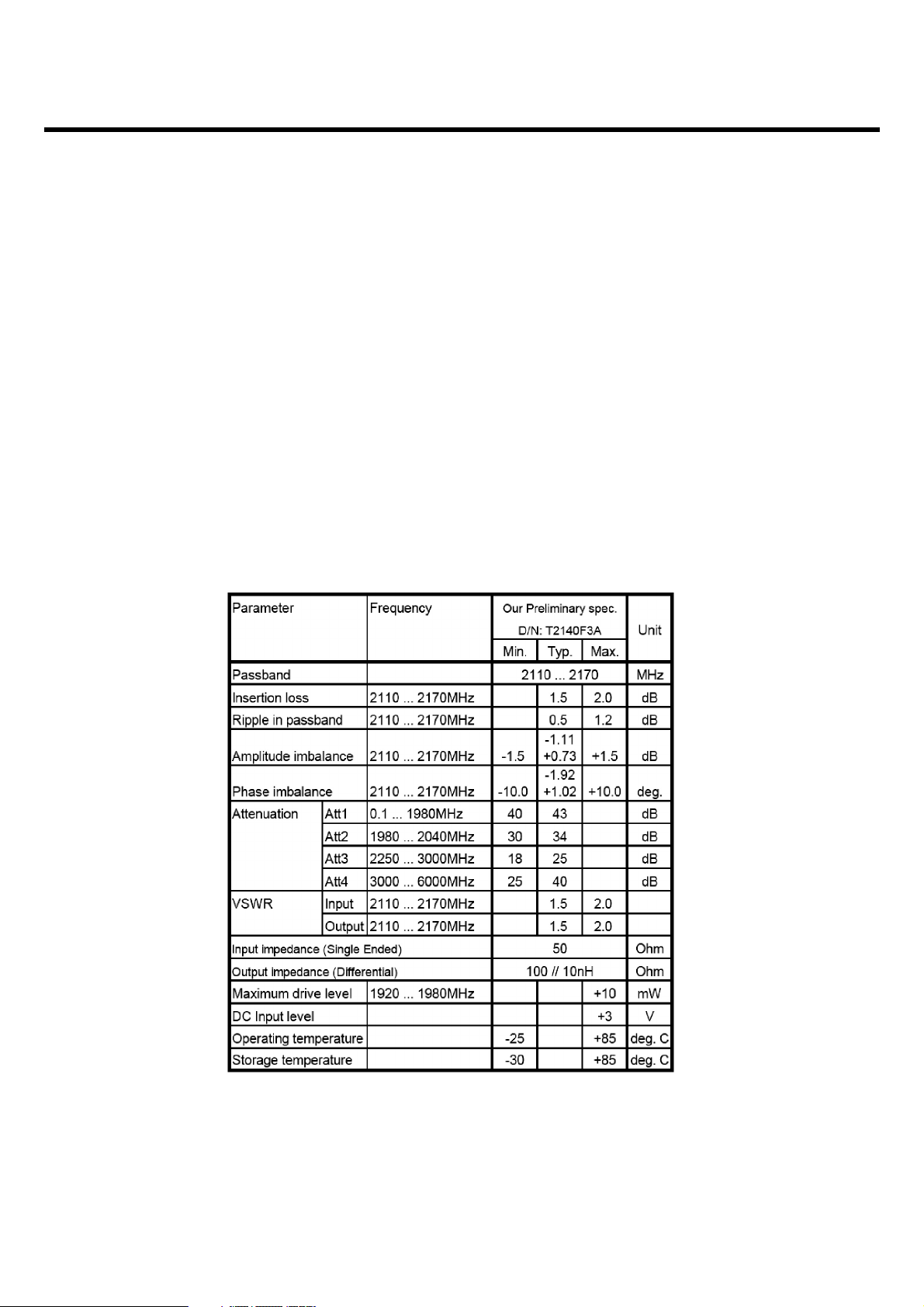
3.5.7 UMTS Rx RF filter (FL502 : EFCH2140TDE1)
• Frequency range : 2110 ~ 2170MHz
An RF filter is located between the UMTS LNA and mixer. Insertion loss is important, but not as
critical as losses before the LNA. The most important parameters of this component include:
• Out-of-band rejection or attenuation levels, usually specified to meet these conditions:
- Far out-of-band signals - ranging from DC up to the first band of particular concern and from the
last band of particular concern to beyond three times the highest passband frequency.
- Tx-band leakage - the transmitter channel power, although attenuated by the duplexer, still
presents a cross-modulation threat in combination with Rx-band jammers. The RF filter must
provide rejection of this Tx-band leakage.
- Other frequencies of particular concern . bands known to include other wireless transmitters that
may deliver significant power levels to the receiver input.
3. TECHNICAL BRIEF
- 32 -
[Table 1.3] WCDMA Rx SAW Filter Specification
Page 31

LGE Internal Use Only
Copyright © 2007 LG Electronics. Inc. All right reserved.
Only for training and service purposes
3. TECHNICAL BRIEF
- 33 -
3.5.8 Bluetooth (U403 : BCM2048SKUFBG)
The bluetooth components are an bluetooth module and Antenna. Figure1.5.12-1 shows the bluetooth
system architecture in the KS20.
[Figure1.9] Bluetooth system architecture
Page 32

- 34 -
3. TECHNICAL BRIEF
3.5.9 WLAN (SWL-2700S)
The MSM7200 supports SDIO interface which can be used for WLAN baseband data communication
with a WLAN module. Because WLAN module includes RF components, the RF parts for KS20 WLAN
include only WLAN module and an antenna. Figure 1.10 shows KS20 WLAN system architecture.
LGE Internal Use Only
Copyright © 2007 LG Electronics. Inc. All right reserved.
Only for training and service purposes
[Figure1.10] WLAN system architecture
Page 33

- 35 -
3. TECHNICAL BRIEF
3.6 Digital Baseband(DBB/MSM7200)
3.6.1 General Description
A. Features(MSM7200)
• Support for multimode operation - WCDMA(UMTS),GSM/GPRS,EDGE, HSDPA
• The ARM1136-J microprocessor can operate at up to 400 MHz.
• The ARM926EJ-S microprocessor can operate up to 256 MHz.
• Internal 256 MBits stacked DDR memory.
• Java hardware acceleration for faster Java-based games and other applets.
• Supports low-power, low-frequency crystal to enable TCXO shutoff.
• Integrated USIM Controller for direct interface to USIM card
• Software-controlled power management feature
• Integrated Bluetooth 2.0 baseband processor for wireless connectivity to peripherals
• High-speed, serial mobile-display, digital interface that optimizes the interconnection cost between
the MSM device and the LCD panel
• Receive chain diversity support for WCDMA, providing improved capacity and data throughput
• USB OTG core supports both slave and limited host functionality
• Integrated wideband stereo CODEC for digital audio applications
• Direct interface to digital camera module with video front end (VFE) image processing
• Vocoder support (GSM-HR, FR, EFR, AMR, W-AMR, and 4GV)
• Advanced 15 x 15 x 1.4 mm, 0.5 mm pitch, 543-pin lead-free CSP packaging technology
• HSDPA Features
- supports release 5, December 2004 standard for HSDPA
- HSDPA enables PS data speeds up to 7.2 Mbps on the downlink
• WCDMA Features
- supports release 99 June 2004 of the W-CDMA FDD standard
- PS data rates supporting 384kbps DL / 384kbps UL
- CS data rates supporting 64kbps DL / 64kbps UL
- AMR (all rates)
LGE Internal Use Only
Copyright © 2007 LG Electronics. Inc. All right reserved.
Only for training and service purposes
Page 34

LGE Internal Use Only
Copyright © 2007 LG Electronics. Inc. All right reserved.
Only for training and service purposes
• GSM Features
- Voice features (FR,EFR,AMR,HR)
- Circuit-switched data features(9.6K,14.4K,Fax)
• GPRS Features
- Simple Class A operation
- Multi-slot class 12 data services
- CS schemes CS1,CS2,CS3,CS4
• EDGE Features
- EDGE E2 power class for 8PSK
- Simple Class A, multi-slot class 12
- Downlink/Uplink coding schemes (CS1-4, MCS1-9)
• Operation and Services
- LCD & Camera Interface
- USIM Interface
- Dual Memory Buses(EBI1-SDRAM & EBI2-NAND Flash)
- External Memory Interface (Micro SD)
• Data Communication
- BlueTooth
- Slave USB
3. TECHNICAL BRIEF
- 36 -
Page 35

LGE Internal Use Only
Copyright © 2007 LG Electronics. Inc. All right reserved.
Only for training and service purposes
3. TECHNICAL BRIEF
- 37 -
3.7 Hardware Architecture
MSM7200
MSM7200
MCP
MCP
DDR 1G
NAND 2G
2M AF
VGA
2.8î QVGA LCD
Speaker
Receiver
T Flash
- Touch Controller
- Joy Stick
- Send, End, Hot, Power
-Vol. Up/Down
- Camera Shutter
SIM Card
Int. Mic.
Bluetooth
Bluetooth
WLAN
SWL-2700S
WLAN
SWL-2700S
BCM2048
FM Radio
FM Radio
18Pin Cradle
Connector
18Pin Cradle
Connector
PM7540
PM7540
Battery
Battery
USB
USB
Serial Port
Serial Port
RTC Battery
RTC Battery
1050mAh
RTR6275
XCVR
RTR6275
XCVR
WCDMA
PAM
WCDMA
PAM
Switch-
plexer
Switch-
plexer
WCDMA/HSDPA RF Block
GSM
PAM
GSM
PAM
Duplexer
Duplexer
UART1
SDIO1
GPIO
MIC1
SDIO2
UART2
CAMERA
LOUT/
RCV
EBI1/
EBI2
MDDI
RF
UART3
USB1.1
SBI
[Figure1.11] Simplified Block Diagram of System
Page 36

- 38 -
3. TECHNICAL BRIEF
3.7.1. Block Diagram(MSM7200)
LGE Internal Use Only
Copyright © 2007 LG Electronics. Inc. All right reserved.
Only for training and service purposes
MSM7200
CONNECTIVITY
CAMERA
PROCESSING
(Default 8bit
Interface)
GRAPHICS
VIDEO
AUDIO
DUAL MEMORY BUS
ARM1136-J APPS
PLL
APPS QDSP 4
ARM 926ejs
With Jazelle
UMTS, WCDMA,
processor
BT 1.2
processor
Rx ADC
Tx DAC
MP3, AAC,
EVRC, QCELP
AMR, CMX, MIDI
EBI 1 EBI 2
Open GL ES
3D, 2D
MPEG-4
H.263, H.264
Keypad I/F
SD/SDIO1
USB
UART1
UART2 / RUIM1
UART3 / PMIC SBI
Mono
Speaker
Stereo
Headset
MIC
MicroSD
Camera 2M
KEY
PAD
18 PIN
M M I
USB
NAND Flash
2G
SDRAM
1G
LCD
(2.8 inch)
PM7540
GSM/GPRS/EDGE
processor
USIM
4 Bit
JTAG
RF SBI
GPIO
Camera 0.3M
1
8
P
I
N
M
M
I
MDDI
Modem QDSP4
SD/SDIO2
WLAN
[Figure1.12] Simplified Block Diagram of MSM7200
Page 37

LGE Internal Use Only
Copyright © 2007 LG Electronics. Inc. All right reserved.
Only for training and service purposes
3. TECHNICAL BRIEF
- 39 -
3.8. Subsystem(MSM7200)
3.8.1. ARM Microprocessor Subsystem
The MSM7200 device uses an embedded ARM1136-J, ARM926EJ-S microprocessor. This
microprocessor, through the system software, controls most of the functionality for the MSM, including
control of the external peripherals such as the keypad, LCD, SDRAM, and NANDFlash devices.
Through a QUALCOMM proprietary serial bus interface (SBI) the ARM926EJ-S configures and
controls the functionality of the RTR6275 and PM7540 devices..
3.8.2. UMTS Subsystem
The UMTS Subsystem performs the digital UMTS signal processing. Its components include:
• Searcher engine
• Demodulating fingers
• Combining block
• Frame deinterleaver
• Viterbi decoder
• Up-link subsystem
• Turbo decoder
On the down-link channel the UMTS subsystem searches, demodulates, and decodes incoming
CPICH, CCPCH, SCH, and Traffic Channel information. It extracts packet data from the downlink
traffic channel and prepares the packet data for processing. For the up-link, the WCDMA subsystem
processes the packet data and modulates the up-link traffic channel (DCH).
3.8.3. GSM Subsystem
The GSM/GPRS/EGPRS subsystem reuses the MSM6280 GSM core. It performs the digital GSM
signal processing and PA gain controls for GPRS support. The PA output level is controlled by an
analog signal generated on the MSM. In GSM mode, the power profile ramps up before the burst and
ramps down after the burst. In GPRS mode, at the beginning of each burst (up to four active transmit
slots), PA must be smoothly ramped up to some desired output power level, held at that level for the
current slot, smoothly ramped down/up during the transition period and held to the new level for the
next slot until the last slot. Then it must be smoothly ramped down to near-zero level. The MSM6275
support differential GSM PA power control output. The RF interface communicates with the mobile
station external RF circuits. Signals to these circuits control signal gain in the Rx and Tx signal path,
control DC offset errors, and maintain the system frequency reference.
3.8.4. RF Interface
The RF interface communicates with the mobile station’s external RF and analog baseband circuits.
Signals to these circuits control signal gain in the Rx and Tx signal path and maintain The system’s
frequency reference.
Page 38

LGE Internal Use Only
Copyright © 2007 LG Electronics. Inc. All right reserved.
Only for training and service purposes
3. TECHNICAL BRIEF
- 40 -
3.8.5. Serial Bus Interface(SBI)
The MSM7200 device’s SBI is designed specifically to be a quick, low pin count control protocol for
QUALCOMM’s RTR6275 and PM7540 ASICs. Using the SBI, the RTR6275 and PM7540 devices
can be configured for different operating modes and for minimum power consumption, extending
battery life in Standby mode. The SBI also controls DC baseband offset errors.
3.8.6. Wideband CODEC
The MSM7200 device integrates a wideband voice/audio CODEC into the mobile station modem
(MSM). The CODEC supports two differential microphone inputs, one differential earphone output, one
single-ended earphone output, and a differential analog auxiliary interface.
The CODEC integrates the microphone and earphone amplifiers into the MSM6280 device, reducing
the external component count to just a few passive components.
The microphone (Tx) audio path consists of a two-stage amplifier with the gain of the second stage set
externally. The Rx/Tx paths are designed to meet the ITU-G.712 requirements for digital transmission
systems.
3.8.7. Vocoder Subsystem
The MSM7200 device’s QDSP4000 supports AMR,FR,EFR and HR. In addition, the QDSP4000 has
modules to support the following audio functions: DTMF tone generation, DTMF tone detection, Tx/Rx
volume controls, Tx/Rx automatic gain control (AGC), Rx Automatic Volume Control (AVC), EarSeal
Echo Canceller (ESEC), Acoustic Echo Canceller (AEC), Noise Suppression (NS), and programmable,
13-tap, Type-I, FIR, Tx/Rx compensation filters. The MSM7200 device’s integrated ARM9TDMI
processor downloads the firmware into the QDSP4000 and configures QDSP4000 to support the
desired functionality.
3.8.8. ARM Microprocessor subsystem
The MSM7200 device uses an embedded ARM1136-J, ARM926EJ-S microprocessor. This
microprocessor, through the system software, controls most of the functionality for the MSM device,
including control of the external peripherals such as the keypad, LCD, RAM, ROM, and EEPROM
devices. Through a generic serial bus interface (SBI) the ARM926EJ-S configures and controls the
functionality of the RTR6275 and PM7540 devices.
Page 39

LGE Internal Use Only
Copyright © 2007 LG Electronics. Inc. All right reserved.
Only for training and service purposes
3. TECHNICAL BRIEF
- 41 -
3.8.9. Mode Select and JTAG Interfaces
The mode pins to the MSM7200 device determine the overall operating mode of the ASIC. The options
under the control of the mode inputs are Native mode, which is the normal subscriber unit operation,
ETM mode, which enables the built-in trace mode, and test mode for factory testing. The MSM7200
device meets the intent of the ANSI/IEEE 1149.1A-1993 feature list. The JTAG interface can be used
to test digital interconnects between devices within the mobile station during manufacture.
3.8.10. General-Purpose Input/Output Interface
The MSM7200 device has general-purpose bidirectional input/output pins. Some of the GPIO pins
have alternate functions supported on them. The alternate functions include USB interface, additional
RAM, ROM, general-purpose chip selects, parallel LCD interface, and a UART interface. The function
of these pins is documented in the various software releases.
3.8.11. UART
The MSM7200 device employs three UARTs. UART1 has dedicated pins while UART2 and UART3
share multiplexed pins.
• UART1 for Bluetooth
• UART2 for USIM interface
• UART3 for data
3.8.12. USB
The MSM7200 device integrates a universal serial bus (USB) controller that supports both
unidirectional and bidirectional transceiver interfaces. The USB controller acts as a USB peripheral
communicating with the USB host.
Page 40

- 42 -
3. TECHNICAL BRIEF
3.9. Power Block
3.9.1. General
MSM7200, included RF, is fully covered by PM7540(Qualcomm PMIC). PM7540 cover the power of
MSM7200, MSM memory, RF block, Bluetooth, USIM and TCXO. Major power components are :
PM7540(U304) : Phone power supply
MAX8645Y(U702) : LCD Backlight/Flash charge pump
3.9.2. PM7540
The PM7540 device (Figure) integrates all wireless handset power management. The power
management portion accepts power from all the most common sources - battery, external charger,
adapter, coin cell back-up - and generates all the regulated voltages needed to power the appropriate
handset electronics. It monitors and controls the power sources, detecting which sources are applied,
verifying that they are within acceptable operational limits, and coordinates battery and coin cell
recharging while maintaining the handset electronics supply voltages. Eight programmable output
voltages are generated using low dropout voltage regulators, all derived from a common trimmed
voltage reference.
A dedicated controller manages the TCXO warm-up and signal buffering, and key parameters (undervoltage lockout and crystal oscillator signal presence) are monitored to protect against detrimental
conditions.
MSM device controls and statuses the PM7540 IC using Single Serial Bus Interface (SSBI)
supplemented by an Interrupt Manager for time-critical information. Another dedicated IC Interface
circuit monitors multiple trigger events and controls the power-on sequence.
LGE Internal Use Only
Copyright © 2007 LG Electronics. Inc. All right reserved.
Only for training and service purposes
Page 41

- 43 -
3. TECHNICAL BRIEF
LGE Internal Use Only
Copyright © 2007 LG Electronics. Inc. All right reserved.
Only for training and service purposes
[Figure1.13] PM7540 Functional Block Diagram
Page 42

- 44 -
3. TECHNICAL BRIEF
3.9.3. Charging control
A programmable charging block in PM7540 is used for battery charging. It is possible to set limits for
the charging current. The external supply typically connects directly to pin (VCHG). The voltage on this
pin (VCHG) is monitored by detection circuitry to ascertain whether a valid external supply is applied or
not. For additional accuracy or to capture variations over time, this voltage is routed internally to the
housekeeping ADC via the analog multiplexer. PM7540 circuits monitor voltages at VCHARGER and
ICHARGE pins to determine which supply should be used and when to switch between the two
supplies. These pins are connected to the Source (or emitter) and Drain (or collector) contacts of the
pass transistor respectively.
LGE Internal Use Only
Copyright © 2007 LG Electronics. Inc. All right reserved.
Only for training and service purposes
100~76 (%) 75~51 (%)
50~26 (%) 25~6 (%)
5~0 (%)
PM7540
Input Power
Management
KS20 Battery Bar Display(Stand By Condition)
Page 43

- 45 -
3. TECHNICAL BRIEF
Trickle Charging
Trickle Charging of the main battery, enabled through SBI control and powered from V
DD,
is provided by
the PM7540 IC, The trickle charger is on-chip programmable current source that supplies current from
VDDto pin (VBAT). Trickle charging can be used for lithium-ion and nickelbased batteries, with its
performance specified below (3.2V). The charging current is set to 80mA.
LGE Internal Use Only
Copyright © 2007 LG Electronics. Inc. All right reserved.
Only for training and service purposes
Parameter Min Typ Max Unit
Trickle Current 60 80 100 mA
PM7540
Input Power
Managemen
t
Page 44

- 46 -
3. TECHNICAL BRIEF
Constant Current Charging
The PM7540 IC supports constant current charging of the main battery by controlling the charger pass
transistor and the battery transistor. The constant current charging continues until the battery reaches
its target voltage, 4.2V.
Constant Voltage Charging
Constant voltage charging begins when the battery voltage reaches a target voltage, 4.2V.
The end of constant voltage charging is commonly detected 10% of the full charging current.
• Charging Method : CC & CV (Constant Current & Constant Voltage)
¶U Maximum Charging Voltage : 4.2V
¶U Maximum Charging Current : 900mA
¶U Nominal Battery Capacity : 1050mAh
¶U Charging time : Max 2.5h (Except time trickle charging)
¶U Full charge indication current (icon stop current) : 60mA
¶U Cut-off voltage : 3.20V
LGE Internal Use Only
Copyright © 2007 LG Electronics. Inc. All right reserved.
Only for training and service purposes
Page 45

- 47 -
3. TECHNICAL BRIEF
LGE Internal Use Only
Copyright © 2007 LG Electronics. Inc. All right reserved.
Only for training and service purposes
3.10. External memory interface
A. MSM7200
The MSM7200 device was designed to provide two distinct memory interfaces. EBI1 was targeted for
supporting DDR synchronous memory devices. EBI2 was targeted towards supporting slower
asynchronous devices such as LCD, NAND flash, SRAM, NOR flash etc. To support the highbandwidth, high-density, and low-latency requirements of the advanced on-chip applications, the
MSM7200 IC has two high-speed, high-performance memory slave interfaces: the external bus
interface 1 (EBI1) and the stack memory interface (SMI). To achieve higher bandwidth and better use
of the memory device interface, the SMI accepts multiple commands for the external memory device.
The SMI interface acts as a slave device to all of the bus masters within the MSM device. The masters
arbitrate to gain access to the SMI, and upon obtaining the access, they issue commands to the SMI.
The bus masters are connected to the SMI through an advanced extensible interface (AXI) bus bridge
(or global interconnect block) and communicate over a 64-bit, non-blocking AXI bus protocol. The AXI
bus bridge provides the arbitration logic for all of the bus masters.
•
EBI1 Features
- Support for only low-power memories at 1.8-V I/O power supply voltage
- AXI bus frequencies up to 133 MHz
- A 16-bit/32-bit static and dynamic memory interface
•
DDR SDRAM interface features include:
- Supports both 32-bit DDR SDRAM devices, up to 133-MHz bus speed
- Supports auto precharge and manual precharge
- Supports partial refresh
- Separate CKE pin per chip-select to support partial operation mode
- Idle powerdown to save idling power consumption
•
EBI2 Features
- Support for asynchronous FLASH and SRAM(16bit & 8bit).
- Interface support for byte addressable 16bit devices(UB_N & LB_N signals).
- 2Mbytes of memory per chip select.
- Support for 8 bit/16bit wide NAND flash.
- Support for parallel LCD interfaces, port mapped of memory mapped(8 or 16 bit)
•
Multi Chip Package : DDR SDRAM and NAND Flash merged 1 package
•
2Gb NAND(8bit) flash memory + 1Gb DDR SDRAM (32bit)
Interface Spec
Device Part Name Maker Read Access Time Write Access Time
NAND SS 45 ns 200 us
SDRAM 7.5 ns 7.5 ns
[Table 1.4] External memory interface for KS20
KAL009001M-D1YY SS
Page 46

- 48 -
3. TECHNICAL BRIEF
LGE Internal Use Only
Copyright © 2007 LG Electronics. Inc. All right reserved.
Only for training and service purposes
[Figure1.14] Simplified Block Diagram of Memory Interface
MSM7200
DDR
SDRAM
1Gb
(128MB)
NAND
2Gb
(256MB)
DATA[31:0]
ADDRESS[15:
0]
WE*
CS*
CAS*
RAS*
CLK_EN
CLK[0:1]
DQM[3:0]
DQS[3:0]
NAND_CS*
NAND_RE*
NAND_WE*
NAND_CLE
NAND_WP*
NAND_ALE
NAND_READY
DATA[7:0]
EBI1
EBI2
Page 47
- 49 -
3. TECHNICAL BRIEF
LGE Internal Use Only
Copyright © 2007 LG Electronics. Inc. All right reserved.
Only for training and service purposes
3.11. H/W Sub System
3.11.1. RF Interface
A. RTR6275(WCDMA_Tx, GSM_Tx/Rx)
MSM7200 controls RF part(RTR6275) using these signals.
• SSBDT : SSBI I/F signals for control Sub-chipset
• TX_ON : Power AMP on RF part
• RX0_I/Q_M/P,TX_I/Q_M/P : I/Q for T/Rx of RF
• TX_AGC_ADJ : control the gain of the Tx signal prior to the power amplifier
• DAC_REF : Reference input to the MSM Tx data DACs
[Figure1.15] Block Diagram of RF Interface
Page 48

- 50 -
3. TECHNICAL BRIEF
LGE Internal Use Only
Copyright © 2007 LG Electronics. Inc. All right reserved.
Only for training and service purposes
B. the others
• TRK_LO_ADJ : TCXO(19.2M) Control
• PA_ON0/PA_RANGE0 : WCDMA(2100) TX Power Amp Enable
• ANT_SEL[0-2] : Ant Switch Module Mode Selection(WCDMA,GSM Tx/Rx,DCS-PCS Tx/Rx)
• GSM_PA_BAND : GSM/DCS-PCS Band Selection of Power Amp
• GSM_PA_RAMP : Power Amp Gain Control of APC_IC
• GSM_PA_EN : Power Amp Gain Control Enable of APC_IC
Page 49

- 51 -
3. TECHNICAL BRIEF
LGE Internal Use Only
Copyright © 2007 LG Electronics. Inc. All right reserved.
Only for training and service purposes
3.11.2. MSM Sub System
3.11.2.1. USIM Interface
SIM interface scheme is shown in Figure.
And, there control signals are followed
• USIM_CLK : USIM Clock
• USIM_Reset : USIM Reset
• USIM_Data : USIM Data T/Rx
3.11.2.2. UART Interface
UART signals are connected to MSM GPIO through IO connector with 115200 bps speed.
MSM7200
PM7540
USIM
USIM CLK
USIM Reset
USIM Data
USIM Data
USIM Reset
USIM CLK
VREG_UIM 2.85V
[Figure1.16] SIM Interface
GPIO_Map Name Note
GPIO_86 UART3_RX Data_Rx
GPIO_87 UART3_TX Data_Tx
[Table 1.5] UART Interface
Page 50

- 52 -
3. TECHNICAL BRIEF
LGE Internal Use Only
Copyright © 2007 LG Electronics. Inc. All right reserved.
Only for training and service purposes
3.11.2.3. USB
The MSM7200 device contains a Universal Serial Bus (USB) interface to provide an efficient
interconnect between the mobile phone and a personal computer (PC). The USB interface of the
MSM7200 was designed to comply with the definition of a
peripheral as specified in USB Specification, Revision 1.1. Therefore, by definition, the USB interface
is also compliant as a peripheral with the USB Specification, Revision 2.0.
The USB Specification Revision 1.1 defines two speeds of operation, namely low-speed (1.5 Mbps)
and full-speed (12 Mbps), both of which are supported by the MSM7200.
Name Note
MSM_USB1_VM Data to/from MSM
MSM_USB1_VP Data to/from MSM
nUSB_OE1 Out-Put Enable of Transceiver
VUSB_5.0V USB_Power From Host(PC)
CRADLE_USB_DP USB Data+ to Host
CRADLE_USB_DN USB Data- to Host
[Table 1.6] USB Signal Interface
[Figure1.17] USB block(MSM7200 Side & PM7540 Side)
MSM7200
PM7540
nUSB_OE1
MSM_USB1_VM
MSM_USB1_VP
CRADLE_USB_DN
CRADLE_USB_DP
VUSB_5.0V
MMI
Conn.
(18p)
Page 51

- 53 -
3. TECHNICAL BRIEF
LGE Internal Use Only
Copyright © 2007 LG Electronics. Inc. All right reserved.
Only for training and service purposes
3.11.3. Key Pad
There are 13 main key buttons that are controlled by MSM7200. Refer to the Keypad circuit. ‘Power
Button’ Key is connected to PMIC(PM7540:GPIO83).
Power Button
KB105
D119
PRSB6.8C
INSTPAR
KPDPWR_ON
[Table 1.7] Key Matrix Mapping Table
[Figure1.18] Power Button Keypad circuit
Page 52

- 54 -
3. TECHNICAL BRIEF
LGE Internal Use Only
Copyright © 2007 LG Electronics. Inc. All right reserved.
Only for training and service purposes
[Figure1.19] Main Keypad Circuit
[Figure1.20] Camera Keypad Circuit
Function Key
Button
SEND
Volume Up
Volume Down
KB104
D111
PRSB6.8C
D102
PRSB6.8C
INSTPAR
KB101
KB100
D112
PRSB6.8C
KB102
PRSB6.8C
D108
INSTPAR
D109
PRSB6.8C
INSTPAR
PRSB6.8C
D101
INSTPAR
KPD_ROW3
KPD_ROW2
KPD_ROW1KPD_COLUMN1
KPD_ROW4
Camera Button
SW100
LS50D23
ESCY0004201
1
23
4
KPD_ROW2
KPD_ROW1
KPD_COLUMN2
Page 53

- 55 -
3. TECHNICAL BRIEF
LGE Internal Use Only
Copyright © 2007 LG Electronics. Inc. All right reserved.
Only for training and service purposes
END Button
KB103
PRSB6.8C
D110
VA100 EVLC14S02050
EVLC14S02050VA101
KPD_COLUMN2
KPD_ROW0
5-Way Key
INSTPAR
D114
PRSB6.8C
PRSB6.8C
D117
INSTPAR
INSTPAR
D116
PRSB6.8C
INSTPAR
D118
PRSB6.8C
PRSB6.8C
D113
INSTPAR
A
B
C
COM1
COM2COM3
D
E
G1
G2
ESCY0004001
EVQQ7GA50
SW102
PRSB6.8C
D115
INSTPAR
KPD_ROW2
KPD_ROW3
KPD_ROW4
KPD_ROW1KPD_COLUMN0
KPD_ROW0
[Figure1.21] END Keypad Circuit
[Figure1.22] 5-Way Keypad Circuit
Page 54

- 56 -
3. TECHNICAL BRIEF
LGE Internal Use Only
Copyright © 2007 LG Electronics. Inc. All right reserved.
Only for training and service purposes
3.11.4. Touch Interface
In KS20, 4-wire touch screen panel is used for user input method. Two resistive layers make up a 4wire touch screen panel and are separated by insulating dots. The inside surface of each layer is
coated with a transparent metal oxide coating that generates a gradient across each layer when
voltage is applied.
[Table 1.8] MSM7200 Touch screen connections
[Table 1.9] Recommeded operation conditions
[Figure1.23] Touch screen circuit
TOUCH SCREEN CONNECTOR
PRSB6.8CD104
PRSB6.8CD106
D105 PRSB6.8C
D103 PRSB6.8C
6
CN101
G1
G2
1
2
3
4
5
04-6298-006-000-883
ENQY0008602
TOUCH_X1XR
TOUCH_Y1YD
TOUCH_X2XL
TOUCH_Y2YU
Page 55

- 57 -
3. TECHNICAL BRIEF
LGE Internal Use Only
Copyright © 2007 LG Electronics. Inc. All right reserved.
Only for training and service purposes
3.11.5. Camera Interface
KS20 Installed a 2M Pixel with auto focus and 0.3M Pixel Camera.
The CAM-FPCB with 34pin Board to Board connector (AXK7L34227G) is connected to MSM7200. Its
interface is dedicated camera interface port in MSM7200. The following figure is KS20 camera block
diagram.
FLASH_PWR_ON
CAMERA I/F:
CIF_DATA[7:0]
CIF_LV
CIF_FV
CIF_PCLK
CIF_MCLK
CIF_RESET#
CAM_I2C_SCL
CAM_I2C_SDA
CAM_2M_PWDN
CAM_VGA_PWDN
GPIO I/F:
CAM_PWR_ON
FLASH_PWR_ON
2M CAM
MSM7200
8
CAM_DATA[7:0]
CAM_HSYNC
CAM_VSYNC
CAM_PCLK
CAM_MCLK
CAM_RST#
CAM_I2C_SCL
CAM_I2C_SDA
CAM_2M_PWDN
VGA CAM
CAM_DATA[7:0]
CAM_HSYNC
CAM_VSYNC
CAM_PCLK
CAM_MCLK
CAM_RST#
CAM_I2C_SCL
CAM_I2C_SDA
CAM_VGA_PWDN
CAMERA
POWER
CAMERA
POWER
CAM_PWR_ON
ENF
MAX8631
CAM_PWR_ON
DVDD
IOVDD
LVDD
AVDD
VDD
FLASH LED
FLASH_PWR_ON
CAM_PWR_ON
[Table 1.10] Interface between 2M/VGA Camera Module and MSM7200
Page 56

- 58 -
3. TECHNICAL BRIEF
LGE Internal Use Only
Copyright © 2007 LG Electronics. Inc. All right reserved.
Only for training and service purposes
The following figures show the flow of camera I/F signals between MSM7200 and camera modules.
The CAM-FPCB with 34pin Board to Board connector (AXK7L34227G) is connected to MSM7200. Its
interface is dedicated camera interface port in MSM7200.
[Figure1.24] Camera FPCB circuit
2M CAM CONNECTOR (T=0.9. SOCKET)
VCAM2_2.6V
VCAM_1.8V
VCAM3_2.6V
7
8
9
22
23
24
25
26
27
28
29
3
30
31
32
33
34
4
5
6
G4
1
10
11
12
13
14
15
16
17 18
19
2
20
21
CN102
AXK7L34227G
ENBY0015601
G1 G2
G3
VCAM1_2.6V
CAM_DATA7
CAM_DATA6
CAM_DATA5
CAM_DATA4
CAM_DATA3
CAM_DATA2
CAM_DATA1
CAM_DATA0
I2C_SDA
I2C_SCL
CAM_PCLK
nCAM_RST
CAM_MCLK
CAM_VSYNC
CAM_HSYNC
CAM_2M_PWDN
FPCB to SUB Connector
VCAM2_2.6V
VCAM1_2.6V
7
8
9
23
24
25
26
27
28
29
3
30
31
32
33
34
4
5
6
G2
1
10
11
12
13
14
15
16
17 18
19
2
20
21
22
VCAM_1.8V
CN103
G1
VCAM3_2.6V
CAM_DATA7
CAM_DATA6
CAM_DATA5
CAM_DATA4
CAM_DATA3
CAM_DATA2
CAM_DATA1
CAM_DATA0
CAM_MCLK
CAM_2M_PWDN
CAM_VSYNC
CAM_HSYNC
I2C_SCL
I2C_SDA
CAM_VGA_PWDN
nCAM_RST
CAM_PCLK
VGA CAM CONNECTOR
9
VCAM3_2.6V
13
14
15
16
17
18
192
20
3
4
5
6
7
8
ENBY0039601
GB042-20S-H10-E3000
CN101
1
10 11
12
VCAM1_2.6V
CAM_DATA3
CAM_DATA2
CAM_DATA1
CAM_DATA0
CAM_VGA_PWDN
nCAM_RST
I2C_SCL
I2C_SDA
CAM_HSYNC
CAM_VSYNC
CAM_PCLK
CAM_MCLK
CAM_DATA4
CAM_DATA5 CAM_DATA6
CAM_DATA7
Page 57

- 59 -
3. TECHNICAL BRIEF
LGE Internal Use Only
Copyright © 2007 LG Electronics. Inc. All right reserved.
Only for training and service purposes
SUB TO FPCB_CAM CONNECTOR (T=0.9. SOCKET)
NA
TP601
C726
R601 2.2K
FB600
FL600 ICVE21184E150R500FR
G15G2
10
INOUT_A1
1
2
INOUT_A2
INOUT_A3
3
4
INOUT_A4
9
INOUT_B1
INOUT_B2
8
7
INOUT_B3
INOUT_B4
6
VCAM_1.8V
2
INOUT_A2
INOUT_A3
3
4
INOUT_A4
9
INOUT_B1
INOUT_B2
8
7
INOUT_B3
INOUT_B4
6
FL603 ICVE21184E150R500FR
G15G2
10
INOUT_A1
1
R621 0
R719
2.2K
FB601
INOUT_B4
VCAM_2.6V
2.2K
R718
5
G110G2
1
INOUT_A1
INOUT_A2
2
3
INOUT_A3
INOUT_A4
4
INOUT_B1
9
8
INOUT_B2
INOUT_B3
7
6
ICVE21184E150R500FRFL602
32
33
34
4
5
6
7
8
9
18
19
2
20
21
22
23
24
25
26
27
28
29
3
30
31
CN601
AXK7L34227G
ENBY0015601
G1 G2
G3 G4
1
10
11
12
13
14
15
16
17
FB602
2.2KR602
NA
C725
VCAM_2.6V
1
INOUT_A1
INOUT_A2
2
3
INOUT_A3
INOUT_A4
4
INOUT_B1
9
8
INOUT_B2
INOUT_B3
7
6
INOUT_B4
ICVE21184E150R500FRFL604
5
G110G2
VCAM_2.6V
TP600
VCAM_2.6V
0R603
DEFAULT_NET_TYPE
CAM_2M_PWDN
I2C_SCL
I2C_SDA
CAM_VGA_PWDN
CAM_PCLK
nCAM_RST
CAM_MCLK
CAM_DATA7
CAM_DATA6
CAM_DATA5
CAM_DATA4
CAM_DATA3
CAM_DATA2
CAM_DATA1
CAM_DATA0
CAM_VSYNC
CAM_HSYNC
LCD BL/FLASH LED/CAMERA LDOs
C715
10u
C716
1u
10u
C717
5
LDO2
16
M1
M2
15
M3
14
13
M4
OUT
25
28
P1
P2
17
24
PGND
1
PIN
6
REFBP
7
SETF
8
SETM
BGND
29
22
C1N
C1P
23
C2N
27
26
C2P
ENF
21
18
ENLDO
20
ENM1
ENM2
19
F1
12
11
F2
10
F3
9
F4
GND
3
IN
2
LDO1
4
EUSY0263101
MAX8631XETIU702
2.2u
C722
C714
1u
R712 100K
R720
DNI
6.8KR730
R710 100K
VCAM_2.6V
VPWR
R717 13K
2.2u
C721
0.01u
C720
VCAM_1.8V
100KR711
BL_PWR_ON
FLASH_PWR_ON
CAM_PWR_ON
VOUT
BLED4
BLED1
BLED2
BLED3
FLED
[Figure1.25] Camera module I/F and Camera LDO circuit
Page 58

- 60 -
3. TECHNICAL BRIEF
LGE Internal Use Only
Copyright © 2007 LG Electronics. Inc. All right reserved.
Only for training and service purposes
The 2 MEGA Camera module is connected to CAM-FPCB with 34pin Board to Board connector
(AXK7L34227G). Its interface is dedicated camera interface port in MSM7200. The camera port
supply 24.576MHz master clock to camera module and receive 49.152MHz pixel clock (15fps),
vertical sync signal, horizontal sync signal, reset signal and 8bits data from camera module. The
camera module is controlled by I2C port from MSM7200.
[Table 1.11] Interface of 2 MEGA AF Camera Module
GNDGNDGND20
Vertical SynchOVSYNC19
Horizontal SynchOHSYNC18
AVDD2I2M_CAM_AVDD_2.6V17
LVDD2I2M_CAM_LVDD_2.6V15
AVDD1I2M_CAM_AVDD_2.6V16
Master Clock(24.576M)ICLKIN21
GNDGNDGND3
GNDGNDGND4
Camera reset signalIM_CAM_RESET_N5
GNDGNDGND6
NC7
I2C DataOI2C_SDA8
I2C ClockOI2C_SCL9
NC10
LVDD1I2M_CAM_LVDD_2.6V14
Camera power downIM_CAM_PWDN13
GNDGNDGND12
NC11
Master Clock(45.152M)ICAM_PCLK2
GNDGNDGND1
NotePortNameNo
AVDD2O2M_CAM_AVDD_2.6V34
AVDD1O2M_CAM_AVDD_2.6V33
CVDD2O2M_CAM_CVDD_1.8V32
DataOCAM_DATA(7)30
CVDD1O2M_CAM_CVDD_1.8V31
GNDGNDGND22
DataOCAM_DATA(0)23
DataOCAM_DATA(1)24
DataOCAM_DATA(2)25
DataOCAM_DATA(6)29
DataOCAM_DATA(5)28
DataOCAM_DATA(4)27
DataOCAM_DATA(3)26
Page 59

- 61 -
3. TECHNICAL BRIEF
LGE Internal Use Only
Copyright © 2007 LG Electronics. Inc. All right reserved.
Only for training and service purposes
The VGA Camera module is connected to LCD FPCB with 20pin Board to Board connector. Its
interface is dedicated camera interface port in MSM7200. The camera port supply 24.576MHz
master clock to camera module and receive 12.288MHz pixel clock (15fps), vertical sync signal,
horizontal sync signal, reset signal and 8bits data from camera module. The camera module is
controlled by I2C port from MSM7200.
Camera I/O PowerIVREG_CAM_2.6V20
Camera I/O PowerIVREG_MSMP_2.6V19
Camera reset signalICAM_RESET_N18
I2C ClockII2C_SCL17
GNDGNDGND15
I2C ClockII2C_SCD16
GNDGNDGND3
Clock for Camera Data Out(12M)OCAM_PCLK4
DataOCAM_DATA(0)5
DataOCAM_DATA(1)6
DataOCAM_DATA(2)7
DataOCAM_DATA(3)8
DataOCAM_DATA(4)9
DataOCAM_DATA(5)10
Horizontal SyncOCAM_HSYNC14
Vertical SynchOCAM_VSYNC13
DataOCAM_DATA(7)12
DataOCAM_DATA(6)11
Master Clock(24M)ICAM_MCLK2
Camera power downiCAM_PWDN1
NotePortNameNo
[Table 1.12] Interface of VGA Camera Module
Page 60

- 62 -
3. TECHNICAL BRIEF
LGE Internal Use Only
Copyright © 2007 LG Electronics. Inc. All right reserved.
Only for training and service purposes
3.11.6. LED(KEY/Indicator) Light
There are 4 White LEDs in Main key backlight circuit, which are driven by KPD_DR_N line from
PM7540.
In addition, there is 1 RGB LED in LED Notification-RGB backlight circuit, which are driven by
KEBY_BACKLIGHT line from MSM7200 GPIO78/84/85.
[Figure1.26] Schematic of Power Keypad back light circuit
[Figure1.27] Schematic of KEY back light circuit
Power Keypad LED
PRSB6.8C
D107
SSC-TWH104-HLS
LD104
VPWR
SSC-TWH104-HLS
LD101
LD102
SSC-TWH104-HLS
R101100ohm
SSC-TWH104-HLS
LD103
R103100ohm
R102100ohm
100ohm
KPD_DRV_N
R100
BLUE
RED
GREEN
LED Notification-RGB
LD100LEMC-S11G
1
2
3
4
VPWR
LEDCB1
LEDCR1
LEDCG1
Page 61

- 63 -
3. TECHNICAL BRIEF
LGE Internal Use Only
Copyright © 2007 LG Electronics. Inc. All right reserved.
Only for training and service purposes
3.11.7. LCD Module Interface
- The LCD module is a Color TFT supplied by EPSON Imaging Devices.
This LCD Module has a 2.8 inch diagonally measured active display area with 240(RGB)X320
resolution. each pixel is divided into Red, Green and Blue sub-pixels and dots which are arranged in
vertical stripes.
* Features
- Display mode(Main LCD) : Normally Black, Transmissive VA mode 265K colors
- LCD Driver IC: S6D0165(SS)
- Driving Method : A-Si TFT Active Matrix
- 4 bit MDDI(Mobile Display Digital interface) I/F
BL_PWR_ON
Charge Pump
BL PWR
LCD_PWR_ON
LDO
LCD PWR
MDDI I/F
MDDI_P_STB_P
MDDI_P_STB_M
MDDI_P_DATA_P
MDDI_P_DATA_M
GPIO
LCD_RESET
FLM(VSYNC)
LCD_PWR_ON
BL_PWR_ON
MSM7200
MDDI I/F
MDDI_STB+
MDDI_STBMDDI_DT+
MDDI_DT-
RESET
FLM(VSYNC)
LCD
POWER
Vci(2.6)
VccIO(1.8)
LCD
BLIGHT
LED(AN)
LED(CA)
2.8 QVGA MDDI LCD
[Figure1.28] LCD Module Block Diagram
Page 62

LGE Internal Use Only
Copyright © 2007 LG Electronics. Inc. All right reserved.
Only for training and service purposes
3. TECHNICAL BRIEF
- 64 -
[Figure1.29] Display/ LCD FPCB I/F and LCD BL circuit
LCD Connector
7
8
9
16
17
18
19
2
20
21
22
23
24
25
26
27
3
4
5
6
ENQY0014201
04-6293-027-001-829
CN702
1
10
11
12
13
14
15
VLCD_2.6V
VLCD_2.6V
C713
0.01u
VLCD_1.8V
TP700
0.01u
C711
2
A
GND
3
NC
5
VCC
61
VCC1
Y
4
FXLP34L6X U700
TP703
C712
2.2u
TP702
VLCD_1.8V
TP701
0
R706
PG05DBTFC
D707
C705
2.2u
2.2u
C710
FLM
BLED2
BLED3
BLED4
MDDI_P_STB_M
MDDI_P_STB_P
MDDI_P_DATA_M
MDDI_P_DATA_P
VOUT
LCD_RESET
BLED1
LCD BL/FLASH LED/CAMERA LDOs
C715
10u
C716
1u
10u
C717
5
LDO2
16
M1
M2
15
M3
14
13
M4
OUT
25
28
P1
P2
17
24
PGND
1
PIN
6
REFBP
7
SETF
8
SETM
BGND
29
22
C1N
C1P
23
C2N
27
26
C2P
ENF
21
18
ENLDO
20
ENM1
ENM2
19
F1
12
11
F2
10
F3
9
F4
GND
3
IN
2
LDO1
4
EUSY0263101
MAX8631XETIU702
2.2u
C722
C714
1u
R712 100K
R720
DNI
6.8KR730
R710 100K
VCAM_2.6V
VPWR
R717 13K
2.2u
C721
0.01u
C720
VCAM_1.8V
100KR711
BL_PWR_ON
FLASH_PWR_ON
CAM_PWR_ON
VOUT
BLED4
BLED1
BLED2
BLED3
FLED
Page 63

3.11.8. Audio and Sound
3.11.8.1. Overview of Audio & Sound path
LGE Internal Use Only
Copyright © 2007 LG Electronics. Inc. All right reserved.
Only for training and service purposes
3. TECHNICAL BRIEF
- 65 -
[Figure1.30] Audio Path Block Diagram
MSM7200
(U100-1)
SPK
AMP
(U401)
Head_Set
Loud Speaker
MIC
Head_set MIC
Receiver and
Analog
switch
(U400)
Headset
AMP
(U402)
Page 64

LGE Internal Use Only
Copyright © 2007 LG Electronics. Inc. All right reserved.
Only for training and service purposes
3. TECHNICAL BRIEF
- 66 -
3.11.8.2. Audio Signal Processing & Interface
The MSM7200 device integrates a wideband audio CODEC into the mobile station modem. The
wideband codec allows the MSM device to support stereo music/ringer Melody applications in addition
to the 8 kHz voice band applications on the forward link. In the audio transmit path, the device
operates as 13-bit linear converter with software selectable 8 kHz and 16 kHz sampling rate. In the
audio receive path, the device operates as a software selectable 13-bit or 16-bit linear converter with
software selectable 8 kHz, 16 kHz, 22.05 kHz, 24 kHz, 32 kHz, 44.1 kHz, or 48 kHz sampling rate.
Through software, the Rx path can be configured as either a mono or stereo output.
The integrated CODEC contains all of the required conversion and amplification stages for the audio
front end. The CODEC operates as a 13-bit linear CODEC with the transmit (Tx) and receive (Rx)
filters designed to meet ITU-T G.712 requirements. The CODEC includes a programmable sidetone
path for summing a portion of the Tx audio into the Rx path. An on-chip Voltage/Current reference is
provided to generate the precise voltages and currents required by the CODEC. The on-chip voltage
reference also provides a microphone bias voltage required for electret condenser microphones
typically used in handset applications. The MICBIAS output pin is designed to provide 1.8 Volts DC
while delivering as much as 1 mA of current. Audio decoder summing and headset switch detection
are included.
The CODEC interface includes the amplification stages for both the microphone and earphone. The
interface supports two differential microphone inputs and a differential auxiliary input, each of which
can be configured as single-ended if desired. In addition, the interface supports one differential
earphone output, one single-ended earphone output, and one differential auxiliary output or two singleended line outputs. The CODEC is configured through the QDSP4000 command types and is not
directly controlled by the microprocessor. The CODEC configuration command is sent to the
QDSP4000 and then the QDSP4000 executes the command and configures the CODEC. Data is
exchanged between the codec interface and the QDSP4000 through its DMA interface. The
QDSP4000 uses the Ex_DMA_4 channel for reading data from the codec and uses the Ex_DMA_5
channel to transfer data to the codec. The CODEC interface is shown in more detail in Figure below.
[Figure1.31] Audio Interface Detailed Diagram(MSM7200)
Page 65

LGE Internal Use Only
Copyright © 2007 LG Electronics. Inc. All right reserved.
Only for training and service purposes
3. TECHNICAL BRIEF
- 67 -
MSM7200 BLK
C310 22p
390pC308
33p
SD12T1G
D306
C307
D305PG05DBTFC
FB301
C306
1u
DNIR307
C311 22p
390pC309
D307
1
2
34
5
6
PLR0504F
VUSB_5.0V
VBAT
EVLC14S02050VA301
PG05DBTFC D304
C312 1000p
0 R305
FB300
9
14
15
16
17
18
19
2
20
21
22
3
4
5
6
7
8
CN300
ENRY0006001
HSEJ-18S04-25
1
10
11
12
13
R3060
CRADLE_UART_TX
CRADLE_UART_RX
CVBS
nEAR_DET
HS_MIC
VADP_5.0V
FM_ANT
REMOTE_PWR_ON
HSL
HSR
USC2
USC1
Head Set Jack BLK
MIC_Feedback
VMIC_BIAS
R102 2200
NAC104
C106 0.1u
FM_L
FM_R
2200R106
1uC109
H5
B6
Q_IP_CH1
C108 1u
B5
LINE_L_IN
A6
LINE_L_IP
LINE_R_IN
C1
A5
WIPER
LINE_R_IP
E7
D7
AUXIN
C107 0.1u
B7
AUXIP
A7
MIC1N
INTERNAL_MIC_P
HS_MIC
D102
PG05DBTFC
C105 3300p
4.87K/1%
AMUX_OUT
REM_ADC
0.1uC110
U4
D6
E6
F2
F1
B4
MIC2P
MIC1P
MIC2N
HKAIN0
HKAIN1
HKAIN2
RTR_DAC_REF
GSM_PA_DAC_REF
R105 4.7K
TV_OUT
T8
H9
G7
T4
R4
TVOUT
DAC_IREF
HPH_VREF
TVDAC_R_SET
_PWR_CTL_REF
MODEM_RCV_P
MODEM_RCV_N
R103 33
R104 33
HPH_L
HPH_R
RTR_TXIM
G9
P4
B9
A9
HPH_L
HPH_R
I_OUT_N
EAR1_OP
EAR1_ON
C100 27p
RTR_TXIP
RTR_TXQM
P2
P1
N4
I_OUT_P
Q_OUT_P
Q_OUT_N
27pC101
RTR_TXQP
VDD_RX
WLNA_OUT
WCDMA LNA Circuit
C543
L516
22p
1nH
C547
33p
C550
0.75p
FL502
EFCH2140TDE1
L518
3.3nH
5
4
G2
O2
1
IN
G1
O1
2
3
L517
C546
0.5p
WCDMA_MIX_IN_P
1nH
L519
WCDMA_MIX_IN_M
1nH
Page 66

LGE Internal Use Only
Copyright © 2007 LG Electronics. Inc. All right reserved.
Only for training and service purposes
3. TECHNICAL BRIEF
- 68 -
Handset main MIC BLK
Speaker Amp
IN+
A1
IN-
C1
SD_MODE
B2C2
SD_SEL
B1
VDD
A3
VO1
C3
VO2
U401 LM4898ITLX-NOPB
A2
BYPASS
B3
GND
C400
1u
TP400
0.1uC402
1uC403
47KR401
R403 20K
47KR400
C401 0.1u
R402 20K
VPWR
nSPEAKER_SHDN
LINE_ON
LINE_OP
AMP_OUT_N
AMP_OUT_P
GND
5
VCC
10
9
1A1B0
1
2
1B181S
2A
6
3
2B0
2B1
4
7
2S
U400
FSA2267AL10X
VPWR
nRECEIVER_SW
SPKR_P
SPKR_N
MODEM_RCV_N
MODEM_RCV_P
AMP_OUT_P
AMP_OUT_N
Audio Amp for loud Speaker
CN100
OSF213-42DC
SUMY0010508
MIC Connector
1
2
NA
capacitor
D100
INTERNAL_MIC_P
Page 67

LGE Internal Use Only
Copyright © 2007 LG Electronics. Inc. All right reserved.
Only for training and service purposes
3. TECHNICAL BRIEF
- 69 -
3.11.8.3. Audio Mode
There are three audio modes (Voice call, speaker phone, MIDI/MP3).
Headset MP3Headset
Headset MIDI BellHeadset
Speaker MP3Loud Mode
MP3
Speaker MIDI BellLoud Mode
MIDI
Speaker PhoneLoud Mode
Headset Voice CallHeadset
Speaker PhoneLoud Mode
Speaker phone
Receiver Voice Call
Description
Receiver Mode
Voice Call
DeviceMODE
[Table 1.13] Audio Mode
Page 68

LGE Internal Use Only
Copyright © 2007 LG Electronics. Inc. All right reserved.
Only for training and service purposes
Voice Call Receiver Mode Path
3. TECHNICAL BRIEF
- 70 -
MSM7200
(U100-1)
Headset
AMP
(U402)
Head_Set
Analog
switch
(U400)
Receiver and
Loud Speaker
AMP
(U401)
MIC
Head_set MIC
Voice
Voice + MP3 + MIDI
Voice Call Receiver Mode is routed as below
MSM7200 EAR1ON,EAR1OP -> Analog Switch( U400) -> Receiver
Page 69

LGE Internal Use Only
Copyright © 2007 LG Electronics. Inc. All right reserved.
Only for training and service purposes
3. TECHNICAL BRIEF
- 71 -
Voice Call Headset Mode Path & Head video Telephony Mode
Voice Call Headset Mode is routed as below
MSM7200 HPH_L, HPH_R -> 18Pin MMI -> Headset
Voice
Voice + MP3 + MIDI
MSM7200
(U100-1)
AMP
(U401)
Loud Speaker
MIC
Head_set MIC
Receiver and
Analog
switch
(U400)
Head_Set
Headset
AMP
(U402)
Page 70

LGE Internal Use Only
Copyright © 2007 LG Electronics. Inc. All right reserved.
Only for training and service purposes
Voice Call Speaker Phone Mode
3. TECHNICAL BRIEF
- 72 -
MSM7200
(U100-1)
Headset
AMP
(U402)
Head_Set
Receiver and
Loud Speaker
Analog
switch
(U400)
AMP
(U401)
MIC
Head_set MIC
Voice
Voice + MP3 + MIDI
Voice Call Speaker Phone Mode is routed as below
MSM7200 LINE_ON, LINE_OP -> AMP(U401) ->Analog Switch( U400 ) -> Loud speaker
Page 71

LGE Internal Use Only
Copyright © 2007 LG Electronics. Inc. All right reserved.
Only for training and service purposes
3. TECHNICAL BRIEF
- 73 -
MIDI Ring Tone/MP3 (Speaker)
Voice
Voice + MP3 + MIDI
MIDI Ring Tone/MP3 Mode is routed as below
MSM7200 HPH_L -> AMP(U401) -> Loud speaker
MSM7200
(U100-1)
AMP
(U401)
Loud Speaker
MIC
Head_set MIC
Receiver and
Analog
switch
(U400)
Head_Set
Headset
AMP
(U402)
Page 72

LGE Internal Use Only
Copyright © 2007 LG Electronics. Inc. All right reserved.
Only for training and service purposes
MIDI Ring Tone/MP3 (Headset)
3. TECHNICAL BRIEF
- 74 -
MSM7200
(U100-1)
Headset
AMP
(U402)
AMP
(U401)
Head_Set
Analog
switch
(U400)
Receiver and
Loud Speaker
Voice
Voice + MP3 + MIDI
MIDI Ring Tone/MP3 Headset Mode is routed as below
MSM7200 HPH_L, HPH_R -> 18PIn MMI ->Headset
MIC
Head_set MIC
Page 73

LGE Internal Use Only
Copyright © 2007 LG Electronics. Inc. All right reserved.
Only for training and service purposes
3. TECHNICAL BRIEF
- 75 -
Audio & Sound Main Component
There are 6 main components in CU320.
[Table 1.14] Audio main component list
8 ohm receiver & Load
Speaker
EMS1810TPB1PCN701Receiver &
Load Speaker
4
-42 dB microphoneOSF213-42DCCN100MIC5
18Pin MMI ConnectorHSEJ-18S04-25RCN300MMI Conn6
1 Channel Analog SWFSA2267AL10XU400Analog Switch3
Class-AB Audio Amp
Base-Band Modem
Note
LM4898
MSM7200
Maker Part No.
U401
U100
Design No.
Audio amp
MSM7200
Component
2
1
Page 74

- 76 -
3. TECHNICAL BRIEF
3.12. Main Features
1. LG KS20 Main Features
- Bar Type Simple & Stylish design
- UMTS 2100 + GSM 900 + DCS 1800 + PCS 1900 based GSM/GPRS/EDGE/UMTS
- HSDPA 3.6Mbps
- 2.8” QVGA LCD (262K TFT)
- Touch Sensitive User Interface
- Dual Camera (2M Pixel w AF + VGA(0.3M Pixel))
- Stereo Headset & Speaker phone
- 72 Poly Sound
- MP3/AAC/AMR/MIDI/3GP/SMAF decoder and play
- MPEG4 encoder/decoder and play/save
- JPEG en/decoder
- Supports Bluetooth and USB
- Supports WLAN
- Internal User Memory over 128MB
- 1050 mAh (Li-Ion Polymer)
- Windows MobileTM 6 Professional
- Microsoft Office Mobile
LGE Internal Use Only
Copyright © 2007 LG Electronics. Inc. All right reserved.
Only for training and service purposes
Page 75

- 77 -
3. TECHNICAL BRIEF
2. KS20 Main Component
LGE Internal Use Only
Copyright © 2007 LG Electronics. Inc. All right reserved.
Only for training and service purposes
Main board, Top
Main board, Bottom
Sub board, Top
Sub board, Bottom
PMIC BB/MEM/LogicBluetoothRF
Logic
SD/SIM
Socket
WLANCAM
Page 76

- 78 -
3. TECHNICAL BRIEF
LGE Internal Use Only
Copyright © 2007 LG Electronics. Inc. All right reserved.
Only for training and service purposes
KEY-FPCB/Folder Assy, Top
Folder Assy, Bottom
CAM-FPCB
Page 77

- 79 -
3. TECHNICAL BRIEF
RF
LGE Internal Use Only
Copyright © 2007 LG Electronics. Inc. All right reserved.
Only for training and service purposes
FL503
U500
SW500
FL500
ANT501
L504
U403
FL502
U503
X500 U501
FL501
Reference Description Reference Description
U500 RTR6275 FL500 Switch
FL502 UMTS2100 RX SAW filter SW500 Test Connector
FL503 UMTS 2100 Duplexer X500 VCTCXO
U503 UMTS PA U403 Bluetooth RF Transceiver
FL504 UMTS 2100 TX SAW Filter FL501 UMTS2100 RX SAW filter
U501 TX Dual PAM
Page 78

- 80 -
3. TECHNICAL BRIEF
Logic / BB / MEM / Audio
LGE Internal Use Only
Copyright © 2007 LG Electronics. Inc. All right reserved.
Only for training and service purposes
U304
ANT400
U301
CN300
U303
U402
U100
CN301
U201
U300
U302
U400
U401
LD400
Reference Description Reference Description
LD400 Camera Flash U201 Memory, MCP
U304 PMIC, PM7540 U300 Charging/Power Switch
ANT400 Bluetooth ANT. U302 Over-voltage Protection
U301 Switch, UART CN300 MMI Connector(18p)
U303 Switch, USB U402 Audio, Headset Amp
U100 MCU, MSM7200 U400 Audio Sig. Switch
CN301 Battery Connector U401 Audio, Speaker Amp
Page 79

- 81 -
3. TECHNICAL BRIEF
LGE Internal Use Only
Copyright © 2007 LG Electronics. Inc. All right reserved.
Only for training and service purposes
Logic
CN701
CN601
CN700
BAT700
CN600
U702
M600
CN702
CN602
CN603
F1_CN101
F1_CN103
F1_CN102
2M connector(34p)F1_CN102VGA connector(20p)F1_CN101
WLAN Cable connectorSW101
CAM FPCB to Sub
board connector(34p)
F1_CN103
WLAN Cable connectorCN603Backup BatteryBAT700
WLAN AntennaANT100
MICCN100Touch connector(6p)CN101
WLANM600LCD connector(27p)CN702
Sub board to Main
Board connector(90p)
CN602
Sub board to CAM
FPCB connector .
CN601
Vibrator ConnectorCN700Speaker Contact PADU701
Sub Board to KEY
FPCB connector(27p)
CN600
LCD BL/Flash Driver / 2
LDO
U702
DescriptionRef.DescriptionRef.
CN100
CN101
SW101
ANT100
Page 80

- 82 -
4. TROUBLE SHOOTING
4.1 RF Component
TOP SIDE
4. TROUBLE SHOOTING
LGE Internal Use Only
Copyright © 2007 LG Electronics. Inc. All right reserved.
Only for training and service purposes
Page 81

BOTTOM SIDE
- 83 -
4. TROUBLE SHOOTING
LGE Internal Use Only
Copyright © 2007 LG Electronics. Inc. All right reserved.
Only for training and service purposes
Page 82

LGE Internal Use Only
Copyright © 2007 LG Electronics. Inc. All right reserved.
Only for training and service purposes
4. TROUBLE SHOOTING
- 84 -
Page 83

LGE Internal Use Only
Copyright © 2007 LG Electronics. Inc. All right reserved.
Only for training and service purposes
4. TROUBLE SHOOTING
- 85 -
4.2 SIGNAL PATH_UMTS RF
➞ Common Tx/Rx
➞ UMTS 2100 Tx/Rx
➞ UMTS 2100 Tx
➞ UMTS 2100 Rx
➞ Tx I/Q
➞ LO
➞ Rx I/Q
Page 84

LGE Internal Use Only
Copyright © 2007 LG Electronics. Inc. All right reserved.
Only for training and service purposes
4.3 SIGNAL PATH_GSM RF
4. TROUBLE SHOOTING
- 86 -
➞ Common Tx/Rx
➞ GSM900 Tx
➞ DCS/PCS Tx
➞ DCS Rx
➞ PCS Rx
➞ EGSM900 Rx
➞ Tx I/Q
➞ LO
➞ Rx I/Q
Page 85

LGE Internal Use Only
Copyright © 2007 LG Electronics. Inc. All right reserved.
Only for training and service purposes
4. TROUBLE SHOOTING
- 87 -
4.4 Checking VCTCXO Block
The reference frequency (19.2MHz) from X100 (TCXO) is used in UMTS TX
part, GSM part and BB part.
TCXO Circuit
0.1uF
C544
100p C548
VTCXO_2.85V
TG-5010LH_19_2M_75A
EXSK0007802
2
GND3OUT
VCC
4
VCONT
1
X500
19.2MHz
1000p C552
C542
1000p
R517
100ohm
0.01u
C551
TCXO_RTR_19.2MHz
TCXO_PM_19.2MHz
RTR_TRK_LO_ADJ
TP1
TP3
TP4 TP2
Schematic of the TCXO Block
Test Point of the TCXO Block
TP1
TP4
TP3
TP2
Page 86

LGE Internal Use Only
Copyright © 2007 LG Electronics. Inc. All right reserved.
Only for training and service purposes
4. TROUBLE SHOOTING
- 88 -
T
Check C355 of PMIC (U304)
Check R112 of MSM (U100)
T
Page 87

LGE Internal Use Only
Copyright © 2007 LG Electronics. Inc. All right reserved.
Only for training and service purposes
4. TROUBLE SHOOTING
- 89 -
4.5 Checking Front-End Module Block
Rev.F
SFAY0010001
33p
C516
ANT500
33p
C514
33p
C503L500
3.9nH
4.7p
C502
33p
C515
ANT501
VRF_SMPS
C509
0.1u
100nH
L502
13
4
GND4
5
8
GND5
10
GND6
12
GND7
GND8
17
18
GND9
7
NC
22
PCS_RX1
PCS_RX2
21
PGND1
25
PGND2
26
9
UMTS_TX_RX
14
VC1
15
VC2
VC3
16
VDD
ANT
11
DCS_PCS_TX
3
DCS_RX1
20
DCS_RX2
19
EGSM_RX1
24
23
EGSM_RX2
6
EGSM_TX
1
GND1
2
GND2
GND3
FL500
LSHS-M090UE
0
R500
15nH
L501
KMS-506
ENWY0002301
ANT
G1
G2
RF
SW500
NA
C506C505
1.5p
ANT_SEL2
ANT_SEL1
ANT_SEL0
ANT_SEL0
ANT_SEL1
ANT_SEL2
TP1
Schematic of the Front-End Module Block
Test Point of the Front-End Module Block
TP1
Page 88

- 90 -
4. TROUBLE SHOOTING
Logic Table of the FEM
LGE Internal Use Only
Copyright © 2007 LG Electronics. Inc. All right reserved.
Only for training and service purposes
Check VCC
TP1 VRF_SMPS
ANT_SEL0 ANT_SEL1 ANT_SEL2
GSM 850/GSM 900 TX HIGH HIGH LOW
GSM 1800/GSM 1900 TX HIGH LOW LOW
GSM 850 RX - - -
GSM 900 RX LOW LOW LOW
GSM 1800 RX LOW LOW LOW
GSM 1900 RX LOW LOW HIGH
WCDMA HIGH LOW HIGH
Page 89

- 91 -
4. TROUBLE SHOOTING
4.6 Checking UMTS Block
4.6.1 Checking Tx level
LGE Internal Use Only
Copyright © 2007 LG Electronics. Inc. All right reserved.
Only for training and service purposes
ANT500
L500
3.9nH
4.7p
C502
ANT501
0
R500
KMS-506
ENWY0002301
ANT
G1
G2
RF
SW500
NA
C506C505
1.5p
(1608)
10dB
WCDMA LNA Circuit
SMPY0015501
As close as possible
20dB
C565
100p
3p
C554
33p
C561
C560
33p
0.5p
C546
FL503
3
ANT
4
PGNDRX
1
2
TX
SDMY0001301
ACMD-7602
NA
C564
100p
C557
1nH
L519
C566
100p
L516
1nH
C543
22p
L523
10nH
220p
C556
2.7nH
L521
VDD_RX
91
C553
33p
R520
VPWR
33p
C558
R521
91
33p
C549
C563
51
1.5p
R518
VMODE0
3
VMODE1
L518
3.3nH
U503ACPM-7381
6
GND1
GND2
7
GND3
9
PGND
11
RFIN
2
8
RFOUT
VCC1
110
VCC2
VEN
5
4
EFCH2140TDE1
G1
2
G2
5
IN
1
O1
3
O2
4
FL502
L517
1nH
0.75p
10u
C550
C555
EFCH
GG2
3
GO1
4
75
R519
FL5
L515
2.7nH
33p
C547
0.5p
C545
U502
SCDY0003402
50OHM
4
3
COUP IN
2
OUT
1
PWR_DET
WCDMA_PA_ON
WCDMA_PA_R0
WLNA_OUT
For testing, Max power of UMT 2100 is needed.
TP1
TP2
TP3
TP4
Page 90

- 92 -
4. TROUBLE SHOOTING
LGE Internal Use Only
Copyright © 2007 LG Electronics. Inc. All right reserved.
Only for training and service purposes
Run a FTM program
set RF mode to IMT
set uplink freq. To
9750 click Tx on and
WCDMA set PA range
R1 on set Tx AGC to
410
Check Tx SAW
Filter
Check PAM block
Check coupler U103
Check Duplexer
FL104
Check FEM FL100
U502
FL503
FL500
Page 91

- 93 -
4. TROUBLE SHOOTING
4.6.2 Checking UMTS PAM Control Block
• PAM control signal
1. PWR_DET : UMTS Tx Power Detected value (Check R519)
2. TX_AGC_ADJ : UMTS RTR6275 Tx Amp Gain Control
3. +VPWR: UMTS PAM Main Voltage (3V < +VPWR < 4.2V)
4. PA_ON : Turns the PA on and off
5. PA_R0 : Control signals that step the active PA mode and bias
LGE Internal Use Only
Copyright © 2007 LG Electronics. Inc. All right reserved.
Only for training and service purposes
Page 92

LGE Internal Use Only
Copyright © 2007 LG Electronics. Inc. All right reserved.
Only for training and service purposes
4. TROUBLE SHOOTING
- 94 -
4.6.3 Checking RF Rx Level
O
R
TP1
TP2
TP3
Vbias
TP4
WCDMA
RX_WCDMA_2100
L520
1nH
C554
3p
C553
33p
FL503
1
2
TX
ACMD-7602
SDMY0001301
ANT500
ANT501
R500
0
1.5p
L500
3.9nH
C502
4.7p
C506C505
NA
SW500
KMS-506
G2
ANT
RF
G1
ENWY0002301
L515
2.7nH
C545
C549
0.5p
33p
4
PGNDRX
3
ANT
VPWR
U502
C560
SCDY0003402
33p
2
1
C563
OUT
50OHM
1.5p
4
R520
91
20dB
COUP IN
3
R518
51
VDD_RX
C543
L516
22p
1nH
WLNA_OUT
SMPY0015501
C557
C556
C555
10u
100p
220p
(1608)
33p
C561
C564
NA
R519
75
PWR_DET
R521
91
11
PGND
VCC2
9
GND3
8
RFOUT
VMODE1
7
GND2
VMODE0
6
GND1
WCDMA LNA Circuit
L518
C547
3.3nH
33p
C550
0.75p
U503ACPM-7381
110
VCC1
2
RFIN
3
4
5
VEN
C566
As close as possible
100p
FL502
EFCH2140TDE1
C565
100p
5
4
G2
O2
1
IN
G1
O1
2
3
C558
33p
C546
0.5p
L521
2.7nH
10nH
L523
WCDMA_PA_
WCDMA_PA_
Page 93

- 95 -
4. TROUBLE SHOOTING
LGE Internal Use Only
Copyright © 2007 LG Electronics. Inc. All right reserved.
Only for training and service purposes
Check Vbias over 2V?
Check the RF S/W
Check FEM
Check the Duplexer
FL104
Check the RTR6275
Check TP2
Signal exist?
Check TP3
Signal exist?
Check TP4
Signal exist?
FL503
Page 94

- 96 -
4. TROUBLE SHOOTING
4.7 Checking GSM Block
LGE Internal Use Only
Copyright © 2007 LG Electronics. Inc. All right reserved.
Only for training and service purposes
Page 95

- 97 -
4. TROUBLE SHOOTING
4.7.1 Checking RF Tx level
4.7.2 Schematic of RF Tx level
LGE Internal Use Only
Copyright © 2007 LG Electronics. Inc. All right reserved.
Only for training and service purposes
HIGH
(1608)
GSM 900 RX
MODE
WCDMA HIGH
GSM(925-960 MHz)
Rev.F
-
TQM7M5008
DCS(1805-1880 MHz)
ANT_SEL1 ANT_SEL2
HIGH
GSM 1800/GSM 1900 TX
ANTENNA SWITCH MODULE LOGIC
-
GSM 1900 RX
LOW
GSM
GSM 1800 RX
LOW
PCS(1930-1990 MHz)
HIGH
-
LOW
LOW
LOW
SFAY0010001
GSM_PA_BAND
GSM 850/GSM 900 TX
LOW
GSM 850 RX
GSMLOW
LOW
LOW
LOW
DCS/PCS
LOW
LOW
HIGH
HIGH
ANT_SEL0
HIGH
LOW
14
GND6
16
GND7
GND8
17
GSM_IN
7
GSM_OUT
9
3
TX_EN
VBATT
4
VCC
12
6
VRAMP
33p
C516
TQM7M5008
U501
BS
2
DCS_PCS_IN
1
15
DCS_PCS_OUT
GND1
5
8
GND2
GND3
10
11
GND4
13
GND5
ANT500
33p
C540
4.7p
C539
33p
C514
33p
C503L500
3.9nH
4.7p
C502
L514
12nH
33p
C515
ANT501
6.8nH
L513
C534
22u
VRF_SMPS
C509
0.1u
VBAT
100nH
L502
100p
C533
15p
C541
L512
2.2nH
13
4
GND4
5
8
GND5
10
GND6
12
GND7
GND8
17
18
GND9
7
NC
22
PCS_RX1
PCS_RX2
21
PGND1
25
PGND2
26
9
UMTS_TX_RX
14
VC1
15
VC2
VC3
16
VDD
ANT
11
DCS_PCS_TX
3
DCS_RX1
20
DCS_RX2
19
EGSM_RX1
24
23
EGSM_RX2
6
EGSM_TX
1
GND1
2
GND2
GND3
FL500
LSHS-M090UE
0
R500
15nH
L501
KMS-506
ENWY0002301
ANT
G1
G2
RF
SW500
NA
C506
68p
C53
C505
1.5p
ANT_SEL2
ANT_SEL1
ANT_SEL0
TP1
TP2
TP3
Page 96

LGE Internal Use Only
Copyright © 2007 LG Electronics. Inc. All right reserved.
Only for training and service purposes
4.7.3 Checking RF Tx level
4. TROUBLE SHOOTING
- 98 -
Page 97

LGE Internal Use Only
Copyright © 2007 LG Electronics. Inc. All right reserved.
Only for training and service purposes
4. TROUBLE SHOOTING
- 99 -
4.7.4 Checking PAM Block
TP1. GSM_PA_RAMP : Power Amp Gain Control. typically, 0.2V < Vramp < 1.6V
TP2. GSM_PA_EN : Power Amp Enable
(Power ON : higher than 1.25V , Power OFF : lower than 0.4V)
TP3. GSM_PA_BAND : Power Amp Band Selection Control
(GSM Mode : -0.2V < VBS < 0.4V , DCS/PCS Mode : 1.25V < VBS < 3.0V)
TP4. +VPWR : PAM Supply Voltage Vcc higher than 3.0V
Schematic of GSM PAM Block
(1608)
SFSY0030201
TQM7M5008
14
GND6
16
GND7
GND8
17
GSM_IN
7
GSM_OUT
9
3
TX_EN
VBATT
4
VCC
12
6
VRAMP
TQM7M5008
U501
BS
2
DCS_PCS_IN
1
15
DCS_PCS_OUT
GND1
5
8
GND2
GND3
10
11
GND4
13
GND5
33p
C540
2.2K
R510
4.7p
C539
L514
12nH
6.8nH
L513
C534
22u
VBAT
100p
C533
15p
C541
FL501
EFCH897MTDB1
G12G2
3
G3
5
IN
1
O1
4
L512
2.2nH
68p
C538
GSM_PA_BAND
GSM_PA_EN
GSM_PA_RAMP
TP2
TP4
TP3
TP1
Page 98

LGE Internal Use Only
Copyright © 2007 LG Electronics. Inc. All right reserved.
Only for training and service purposes
4.7.5 Checking RF Rx Block
Schematic of `GSM900/DCS/PCS Rx Block
4. TROUBLE SHOOTING
- 100 -
TP1
TP2
TP3
TP3
TP1. DCS RX INPUT
TP2. PCS RX INPUT
TP3. GSM RX INPUT
C503
33p
L502
100nH
DCS_PCS_TX
EGSM_TX
UMTS_TX_RX
DCS_RX2
DCS_RX1
PCS_RX2
PCS_RX1
EGSM_RX2
EGSM_RX1
010001
11
ANT
13
VDD
7
NC
3
6
9
19
20
21
22
23
24
L501
15nH
C509
0.1u
VRF_SMPS
DCS(1805-1880 MHz)
PCS(1930-1990 MHz)
GSM(925-960 MHz)
5.6nHL503
L505 5.6nH
5.6nHL506
5.6nH
L508
27nHL509
L511 27nH
L504
15nH
L507
12nH
L510
33nH
Page 99

LGE Internal Use Only
Copyright © 2007 LG Electronics. Inc. All right reserved.
Only for training and service purposes
4. TROUBLE SHOOTING
- 101 -
Page 100

LGE Internal Use Only
Copyright © 2007 LG Electronics. Inc. All right reserved.
Only for training and service purposes
4.8 Checking Bluetooth Block
Test Point of the Bluetooth Block
Top
Bottom
4. TROUBLE SHOOTING
- 102 -
TP1. VBT_2.6V
TP2. VBT_CORE_2.6V
TP3. TCXO_BT
TP4. BT ANT Output
 Loading...