


Date: February, 2008 / Issue 1.0
Service Manual
Model : KM500
Service Manual
KM500
Internal Use Only

- 3 -
1. Introduction ..................................... 5
1.1 Purpose................................................... 5
1.2. Regulatory Information........................... 5
1.3 Abbreviations .......................................... 7
2. General Performance...................... 8
2.1 Product Name ......................................... 8
2.2 Supporting Standard ................................8
2.3 Main Parts: GSM Solution....................... 8
2.4 HW Feature............................................. 9
2.5 S/W Features .........................................11
3. HW Circuit Description................. 14
3.1 General Description .............................. 14
3.2 RF Part.................................................. 14
3.3 Digital Baseband................................... 20
3.4 Multimedia IC ........................................ 27
3.5 Analog Baseband.................................. 30
3.6 Bluetooth Interface.................................36
3.7 Function difference ................................40
3.8 BOM difference ......................................41
4. Trouble Shooting .......................... 42
4.1 RF Part Technical Brief......................... 43
4.2 RF Part Trouble shooting...................... 46
4.3 Bluetooth Trouble Shooting .................. 54
4.4 Baseband Part Troubleshooting ........... 57
4.5 LCD Display Trouble shooting .............. 65
4.6 Camera Trouble Shooting..................... 72
4.7 Flash LED Trouble Shooting................. 76
4.8 SIM Detect Trouble Shooting................ 79
4.9 Slide Up/Down Trouble Shooting.......... 82
4.10 Speaker/Receiver Trouble Shooting
(Common Path)................................... 84
4.11 MIC Trouble Shooting ......................... 86
4.12 Ear-Mic Jack Detection
Trouble Shooting................................. 88
4.13 Ear-Mic Hook Detection
Trouble Shooting................................. 89
4.14 Ear-Mic Headset MIC
Trouble Shooting................................. 90
4.15 Ear-Mic Headset MIC
Trouble Shooting................................. 91
4.16 FM-Radio Trouble Shooting................ 92
4.17 Transflash Trouble Shooting............... 93
4.18 Main Key Backlight LED
Trouble Shooting................................. 95
4.19 Slide Key Backlight LED
Trouble Shooting................................. 97
4.20 Vibrator Trouble Shooting ................... 98
5. Download..................................... 100
5.1 Download Software............................. 100
5.2 The Environment of Downloading
Software.............................................. 100
5.3 Download Procedure ...........................102
6. Block Diagram............................. 107
7. CIRCUIT DIAGRAM ..................... 109
8. BGA IC Pin Check ........................121
9. PCB LAYOUT............................... 141
10. Calibration
.......................................
151
10.1 What’s the Rx Calibration?
..............
151
10.2 What’s the Tx Calibration?
..............
151
10.3 Calibration program - HOT_KIMCHI 152
11. Engineering Mode......................157
12. EXPLODED VIEW &
REPLACEMENT PART LIST ..... 161
12.1 EXPLODED VIEW ............................ 161
12.2 Replacement Parts
<Mechanic component>.................... 163
<Main component> ........................... 165
12.3 Accessory ......................................... 183
Table of Contents
LGE Internal Use Only
Copyright © 2008 LG Electronics. Inc. All right reserved.
Only for training and service purposes

- 4 -
LGE Internal Use Only
Copyright © 2008 LG Electronics. Inc. All right reserved.
Only for training and service purposes

1.1 Purpose
This manual provides the information necessary to repair, calibration, description and download the features of the KM500.
1.2 Regulatory Information
A. Security
Toll fraud, the unauthorized use of telecommunications system by an unauthorized part (for example, persons other than your
company’s employees, agents, subcontractors, or person working on your company’s behalf) can result in substantial additional
charges you’re your telecommunications services. System users are responsible for the security of own system. There are may
be risks of toll fraud associated with your telecommunications system. System users are responsible for programming and
configuring the equipment to prevent unauthorized use. LGE does not warrant that this product is immune from the above case
but will prevent unauthorized use of common-carrier telecommunication service of facilities accessed through or connected to it.
LGE will not be responsible for any charges that result from such unauthorized use.
B. Incidence of Harm
If a telephone company determines that the equipment provided to customer is faulty and possibly causing harm or interruption in
service to the telephone network, it should disconnect telephone service until repair can be done. A telephone company may
temporarily disconnect service as long as repair is not done.
C. Changes in Service
A local telephone company may make changes in its communications facilities or procedure. If these changes could reasonably
be expected to affect the use of the KM500 or compatibility with the network, the telephone company is required to give advanced
written notice to the user, allowing the user to take appropriate steps to maintain telephone service.
D. Maintenance Limitations
Maintenance limitations on the KM500 must be performed only by the LGE or its authorized agent.
The user may not make any changes and/or repairs expect as specifically noted in this manual.
Therefore, note that unauthorized alternations or repair may affect the regulatory status of the system and may void any remaining
warranty.
E. Notice of Radiated Emissions
The KM500 complies with rules regarding radiation and radio frequency emission as defined by local regulatory agencies. In
accordance with these agencies, you may be required to provide information such as the following to the end user.
- 5 -
1. Introduction
1. Introduction
LGE Internal Use Only
Copyright © 2008 LG Electronics. Inc. All right reserved.
Only for training and service purposes

- 6 -
1. Introduction
F. Pictures
The pictures in this manual are for illustrative purposes only; your actual hardware may look slightly different.
G. Interference and Attenuation
An KM500 may interfere with sensitive laboratory equipment, medical equipment, etc. Interference from unsuppressed engines or
electric motors may cause problems.
H. Electrostatic Sensitive Devices
ATTENTION
Boards, which contain Electrostatic Sensitive Device (ESD), are indicated by the Following information is ESD handling:
•
Service personnel should ground themselves by using a wrist strap when exchange system boards.
•
When repairs are made to a system board, they should spread the floor with anti-static mat which is also grounded.
•
Use a suitable, grounded soldering iron.
•
Keep sensitive parts in these protective packages until these are used.
•
When returning system boards or parts like EEPROM to the factory, use the protective package as described.
LGE Internal Use Only
Copyright © 2008 LG Electronics. Inc. All right reserved.
Only for training and service purposes

- 7 -
1. Introduction
LGE Internal Use Only
Copyright © 2008 LG Electronics. Inc. All right reserved.
Only for training and service purposes
1.3 Abbreviations
For the purposes of this manual, following abbreviations apply:
APC Automatic Power Control
BB KM500
BER Bit Error Ratio
CC-CV Constant Current - Constant Voltage
DAC Digital to Analog Converter
DCS Digital Communication System
dBm dB relative to 1 milliwatt
DSP Digital Signal Processing
EEPROM Electrical Erasable Programmable Read-Only Memory
EL Electroluminescence
ESD Electrostatic Discharge
FPCB Flexible Printed Circuit Board
GMSK Gaussian Minimum Shift Keying
GPIB General Purpose Interface Bus
GSM Global System for Mobile Communications
IPUI International Portable User Identity
IF Intermediate Frequency
LCD Liquid Crystal Display
LDO Low Drop Output
LED Light Emitting Diode
OPLL Offset Phase Locked Loop
PAM Power Amplifier Module
PCB Printed Circuit Board
PGA Programmable Gain Amplifier
PLL Phase Locked Loop
PSTN Public Switched Telephone Network
RF Radio Frequency
RLR Receiving Loudness Rating
RMS Root Mean Square
RTC Real Time Clock
FEM Front End Module
SIM Subscriber Identity Module
SLR Sending Loudness Rating
SRAM Static Random Access Memory
STMR Side Tone Masking Rating
TA Travel Adapter
TDD Time Division Duplex
TDMA Time Division Multiple Access
UART Universal Asynchronous Receiver/Transmitter
VCO Voltage Controlled Oscillator
VCTCXO Voltage Control Temperature Compensated Crystal Oscillator
WAP Wireless Application Protocol

LGE Internal Use Only
Copyright © 2008 LG Electronics. Inc. All right reserved.
Only for training and service purposes
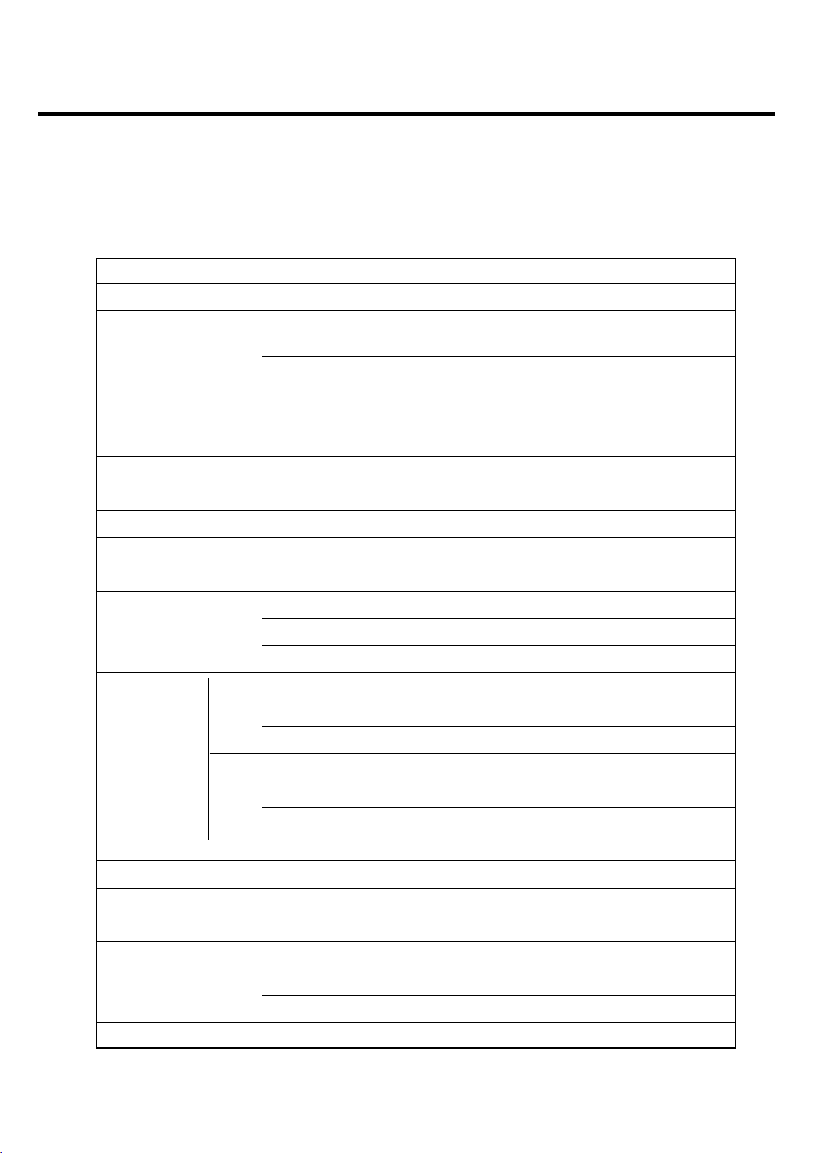
2. General Performance
- 8 -
2. General Performance
2.1 Product Name
KM500: GPRS Class 10 / EDGE Class 10
2.2 Supporting Standard
2.3 Main Parts: GSM Solution
Item Feature Comment
Supporting Standard GSM900/DCS1800/PCS1900
with seamless handover
Phase 2+(include AMR)
SIM Toolkit: Class 1, 2, 3, A-E
Frequency Range GSM900 TX : 880 - 915 MHz
GSM900 RX : 925 - 960 MHz
DCS1800 TX : 1710 - 1785 MHz
DCS1800 RX : 1805 - 1880 MHz
PCS1900 TX : 1850 - 1910 MHz
PCS1900 RX : 1930 - 1990 MHz
Application Standard WAP 2.0, JAVA 2.0
Item Part Name Comment
Digital Baseband Neptune (D761811BZVL): TI
Analog Baseband Triton (TWL3029): TI
RF Chip B6PLD: RENESAS
- 9 -
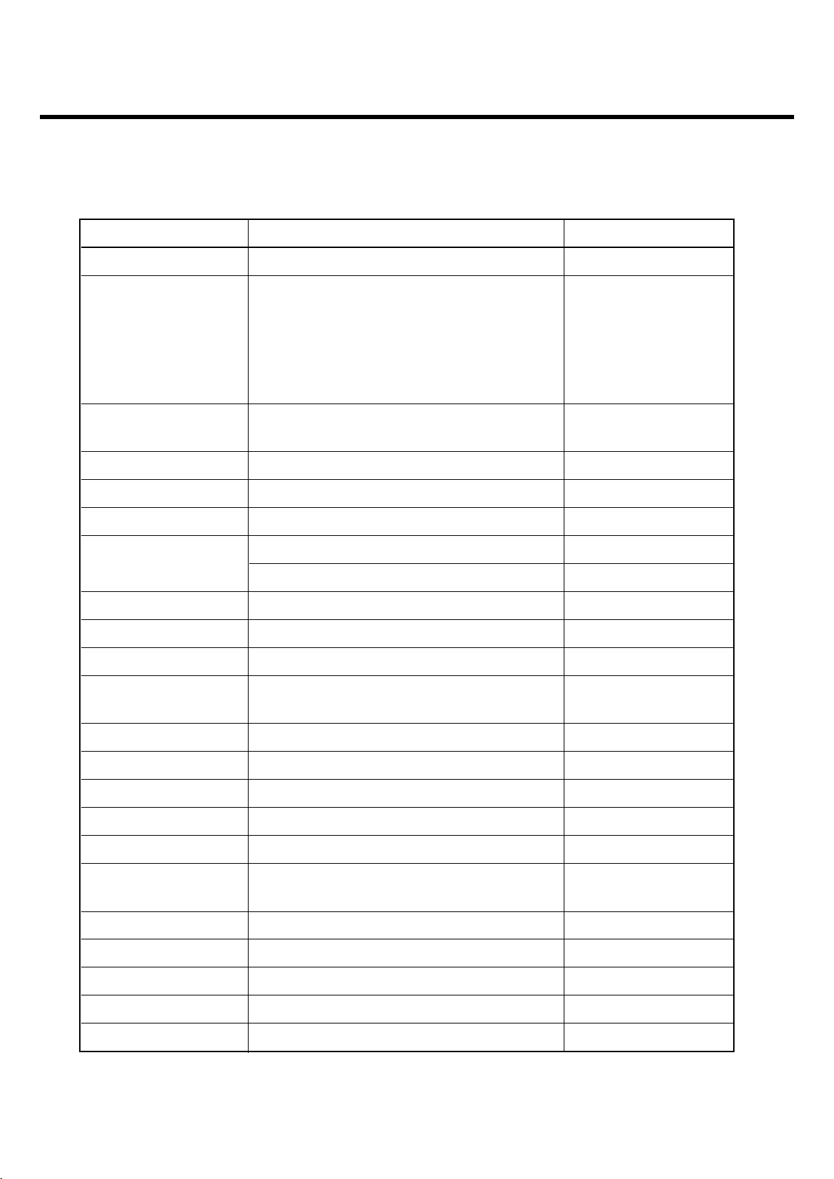
2. General Performance
2.4 HW Feature
LGE Internal Use Only
Copyright © 2008 LG Electronics. Inc. All right reserved.
Only for training and service purposes
Item Feature Comment
Form Factor Slide
Battery 1) Capacity
Standard: Li-Ion, 800mAh
2) Packing Type: Soft Pack
Size Standard:
99.9 x 48 x 14.5 mm
Weight 102 g With Battery
Volume 66.5 cc
PCB Staggered 10Layers , 0.8t
Stand by time 250 hrs @ Paging Period 5
Charging time 3 hrs @ Power Off / 800mAh
Talk time Min: 3.0 hrs @ Power Level 7 @ EGSM / 800mAh
RX sensitivity GSM900: -105 dBm
DCS 1800: -105 dBm
PCS 1900: -105 dBm
TX output power GSM/ GSM900: 32 dBm Class4 (GSM900)
GPRS DCS 1800: 29.5 dBm Class1 (PCS)
PCS 1900: 30 dBm Class1 (DCS)
EDGE GSM900: 27 dBm E2 (GSM900)
DCS 1800: 26 dBm E2 (PCS)
PCS 1900: 26 dBm E2 (DCS)
GPRS compatibility GPRS Class 10
EDGE compatibility EDGE Class 10
SIM card type Plug-In SIM
3V /1.8V
Display Main LCD
262K Color TFT (240 x 320)
Backlight : White LED
Built-in Camera 2M CMOS Camera One button access
- 10 -
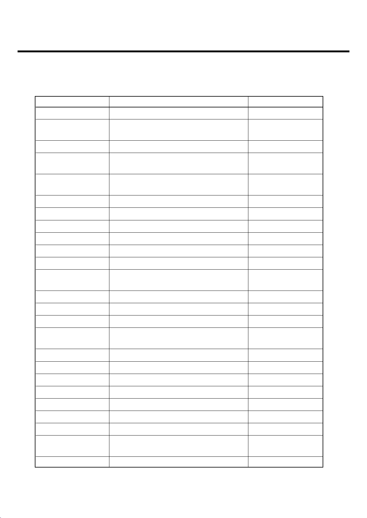
2. General Performance
LGE Internal Use Only
Copyright © 2008 LG Electronics. Inc. All right reserved.
Only for training and service purposes
Item Feature Comment
Status Indicator None
Keypad Alphanumeric Key: 12 Function Key:
Function Key: 14 4 Key Navigation, OK,
Side Key: 4 REW, PLAY, FF, MP3, F1,
Total No of Keys: 30 F2, CLR, SND, END
Side Key: Volume up/down,
CAM, HOLD
ANT Main: Internal Fixed Type
Blue tooth: Internal Fixed Type
System connector 18 Pin
Ear Phone Jack 18pin / 4 Pole, Stereo
PC synchronization Yes
Memory NAND Flash: 1Gbit
SDRAM: 512Mbit
Speech coding FR, EFR, HR, AMR
Data & Fax Built in Data & Fax support
Vibrator Built in Vibrator
Blue Tooth V2.0, HSP, HFP, OPP, FTP(server),
BPP, A2DP, AVRCP
Wi-Fi
802.11b, 802.11g
MIDI(for Buzzer Function) SW Decoded 64Poly
Music Player MP3/ AAC/AAC+ With Graphic EQ
Camcorder MPEG4, H.263, H.264
Voice Recording Yes
Speaker Phone mode Yes
Support
Travel Adapter Yes
CDROM Yes
Stereo Headset Yes Optional
Data Cable Yes Optional
T-Flash (External Memory)
Yes Optional

- 11 -
2. General Performance
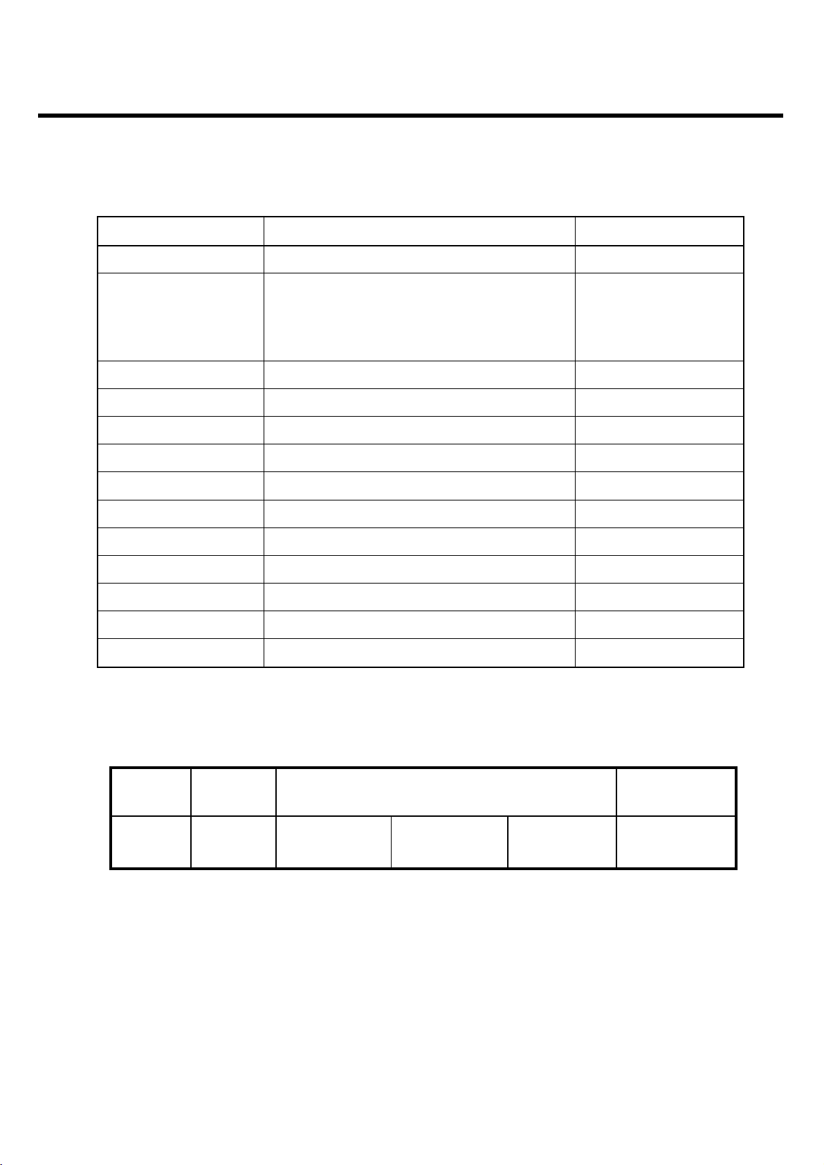
2.5 S/W Features
LGE Internal Use Only
Copyright © 2008 LG Electronics. Inc. All right reserved.
Only for training and service purposes
Item Feature Comment
RSSI 0 ~ 7 Levels
Battery Charging 0 ~ 3 Levels
Key Volume 0 ~ 5 Level
Audio Volume 1 ~ 5 Level
Time / Date Display Yes NITZ
Multi-Language Yes English / French
Quick Access Mode Phone Book / Message / Camera
/ My Stuff / Favorite
PC Sync Schedule / Phonebook / MEMO /
SMS / Download(Photo, file)
Speed Dial Yes (2~9) Voice mail center -> 1 key
Profile Yes
CLIP / CLIR Yes (different melody)
Phone Book 4 Numbers + 1 Memo + 1 e-mail + Total 1000 Member
Group Select + Picture
Last Dial Number Yes (40)
Last Received Number Yes (40)
Last Missed Number Yes (40)
Search by Number/Name Name only
Group 7 Possible Rename
Fixed Dial Number Yes
Service Dial Number Yes
Own Number Yes
Voice Memo
Yes
Call Reminder Yes
Network Selection Automatic
Mute Yes
Call Divert Yes
Call Barring Yes
Call Charge (AoC) No No for Cingular
LGE Internal Use Only
Copyright © 2008 LG Electronics. Inc. All right reserved.
Only for training and service purposes
2. General Performance
- 12 -
Item Feature Comment
Call Duration Yes
SMS (EMS) 100 (10) EMS: Release4
(Except Text align)
SMS Over GPRS Yes
EMS Melody / Picture Yes
Send / Receive / Save
MMS MPEG4 / Send / Yes
Receive / Save
Long Message MAX 925 Characters
Cell Broadcast Yes
Download Over the WAP
Game YES
Calendar Yes
Memo 50
Unit Convert Currency/Area/Length/Volume/Weigh
t/Temperature/Velocity
Tip Calculator No
Wall Paper Yes Default 5ea
WAP Browser Over WAP 2.0 Up Brower Obigo Q-line
Download Melody / Yes Over WAP
Wallpaper
SIM Lock Yes Operator Dependent
SIM Toolkit Class 1, 2, 3, A-E
MMS Yes Open wave MMS Client
EONS Yes
CPHS
Yes V4.2
ENS Yes
Camera Yes 2M F/F / Digital Zoom: x4
JAVA Yes CLDC V1.1 / MIDP V2.0
Download Over WAP
Voice Dial No
- 13 -
2. General Performance
Function difference
LGE Internal Use Only
Copyright © 2008 LG Electronics. Inc. All right reserved.
Only for training and service purposes
Item Feature Comment
IrDa No
Blue tooth Yes V2.0
HSP, HFP, OPP,
FTP(server),
BPP, A2DP, AVRCP
GPRS Yes Class 10
EDGE Yes Class 10
Hold / Retrieve Yes
Conference Call Yes Max. 6
DTMF Yes
Memo pad Yes
TTY No
AMR Yes
Sync ML No
IM No
Email Yes
GSM850/
PCS1900
GSM900/ DCS1800RF Band
Latin
America
Design
Latin
America
Asia / CISEuropeMarket

LGE Internal Use Only
Copyright © 2008 LG Electronics. Inc. All right reserved.
Only for training and service purposes
3. HW Circuit Description
- 14 -
3. HW Circuit Description
3.1 General Description
The RF part consists of a transmitter, a receiver, a synthesizer, a voltage supply and a DCXO part.
The main RF Chipset B6PLD is a highly integrated RF transceiver IC FOR Digital Interface of GSM
850,DCS1800 and PCS1900 quad-band cellular systems. The B6PLD incorporates EDGE transceiver
capability, quad R low-noise amplifiers (LNAs). Direct conversion mixers, a programmable gain
amplifier(PGA) with DC offset and frequency response correction, ADC, Digital filter, Digital Interface,
fully integrated VCOs, an RF fractional-N synthesizer, a low-noise offset PLL transmitter, Digital
modulator, TXDAC, RAMPDAC, and AFCDAC. The B6PLD includes state machine control through
serial programming. All functions operate down to 2.67V and are housed in a 72- pin BGA package.
Hence the B6PLD can form a small size transceiver handset for quad band EDGE transceiver.
3.2 RF Part
3.2.1 Receiver Part
The B6PLD receiver supports quad band, so the front-end incorporates four LNAs and two mixers.
The incoming RF signals are mixed directly down to I/Q baseband by the front-end block. This
incorporates four LNAs/four buffers and two Gilbert Cell mixer blocks optimized for operation at
850MHz, 900MHz, 1800MHz and 1900MHz respectively. The front-end block is followed by two
closely matched baseband amplifier chains.
These include distributed low pass filtering, one switched gain stage and one fixed gain stage. In
addition, the baseband section integrates A/D and D/A converters which provide automatic on-chip
correction of DC offsets.
<Fig.1> Receiver Part Block Diagram

LGE Internal Use Only
Copyright © 2008 LG Electronics. Inc. All right reserved.
Only for training and service purposes
3. HW Circuit Description
- 15 -
3.2.1.1 Baseband PGA/Low pass Filter Specifications
The baseband programmable amplifier comprises one stage with variable gain followed by a fixed
gain amplifier. The overall gain control range is 36dB with 6dB Steps. The filtering is provided by a
single R/C low pass filter with an on-chip capacitor followed by on-chip Chebychev low pass filters.
The filters have been specified to achieve maximal group delay flatness in the pass-band combined
with the required levels of suppression of interfering signals. The distribution of the gain and filtering
has been designed to ensure that the receiver does not compress under blocking conditions. The
final fixed gain amplifier is included to match the on-chip levels to the input dynamic range of the
ADC.
3.2.1.2 DC offset auto-calibration system
B6PLD implements a system for cancelling the DC offsets in the baseband programmable gain
amplifiers(PGA). This prevents a small DC offset at the input giving a large DC offset at the output,
even at high gain settings. When the B6PLD receiver is performing an auto-calibration, the
sequencer cancels the offsets locally around the PGA, then the Digital filter. The system includes
switches to short out the signal path whilst the cancellation is occurring. The switches are opened in
sequence as the calibration progresses. For PGA the A/D converter system employs a successive
approximation technique and achieves 6 bit resolution. The PGA stage has an associated 6 bit
current DAC which cancels the DC offset at the output. The sequencer ensures that on-chip filters
have sufficient time to settle before applying correction in the next digital offset cancellation stage.
LGE Internal Use Only
Copyright © 2008 LG Electronics. Inc. All right reserved.
Only for training and service purposes
3. HW Circuit Description
- 16 -
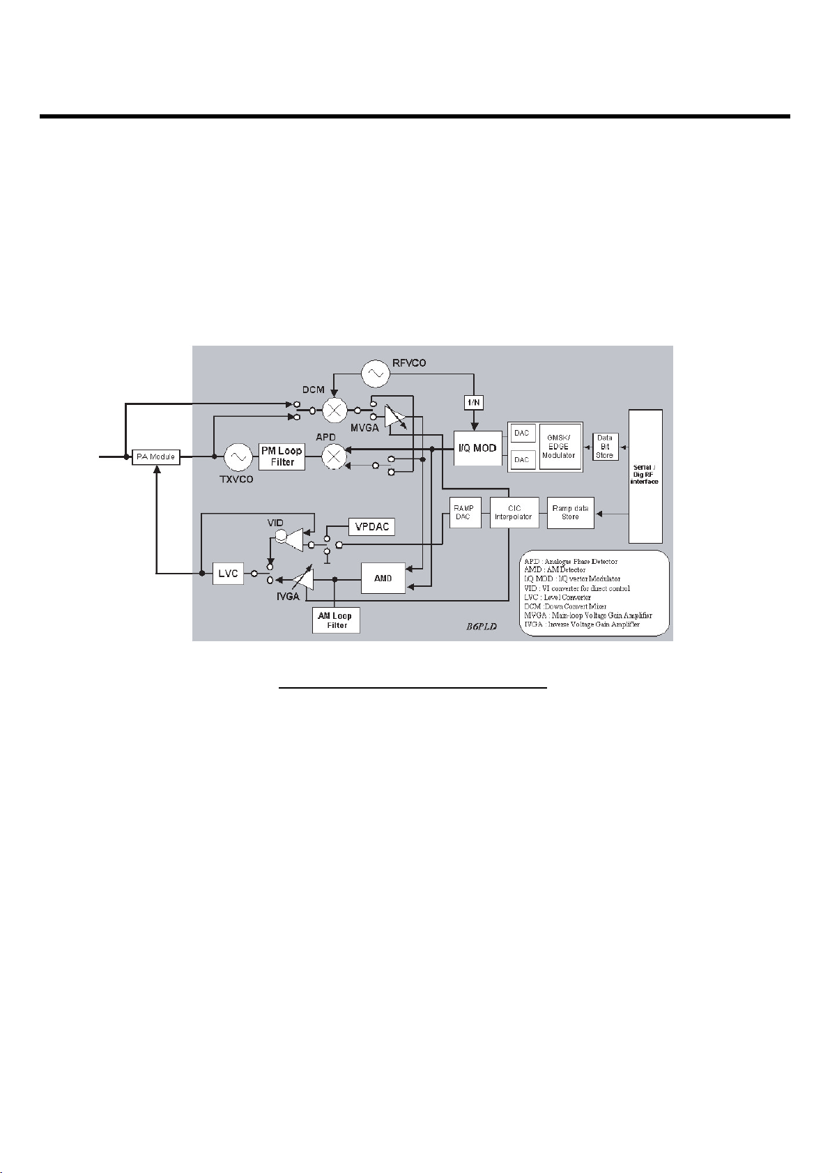
3.2.2 Transmitter part
The B6PLD transmitter is capable of both GMSK and 8-PSK modulation, to support for conventional
GSM and EDGE. B6PLD integrates all loop filters to configure both PM loop and AM loop. See block
diagram below.
3.2.2.1 Polar Loop Structure
Three main functions are identified in the transmitter architecture; I/Q vector modulation at IF
frequency, amplitude and phase loop at IF/RF frequencies and power amplification.
Fig. Simplified Block diagram for Tx part

3.2.3 RF Synthesizer
3.2.4 Front End Module Specification
3.2.4.1 Block Diagram and Internal Matching Condition
LGE Internal Use Only
Copyright © 2008 LG Electronics. Inc. All right reserved.
Only for training and service purposes
3. HW Circuit Description
- 17 -
FEM

LGE Internal Use Only
Copyright © 2008 LG Electronics. Inc. All right reserved.
Only for training and service purposes
3. HW Circuit Description
- 18 -
3.2.4.2 Logic Table for Selection
3.2.5 Power Amplifier Module
for Quad-band GSM/GPRS/EDGE
3.2.5.1 PAM Specification
-. Quad band GSM, GPRS & Polar Loop EDGE Amplifier
-. For 3.5V nominal operation
-. Built-in LDO circuit
-. GPRS Class 12 operation compatible
-. Integrated directional coupler
3.2.5.2 Circuit Diagram and peripheral components
Vc1 Vc2 Current
GSM900_Tx 2.6V 0V 8.0 mA
GSM1800 / 1900_Tx 0V 2.6V 8.0 mA
GSM900_Rx 0V 0V <0.5µA
GSM1800_Rx 0V 0V <0.5µA
GSM1900_Rx 0V 0V <0.5µA
<Table> Band SW Logic Table
PAM
LGE Internal Use Only
Copyright © 2008 LG Electronics. Inc. All right reserved.
Only for training and service purposes
3. HW Circuit Description
- 19 -
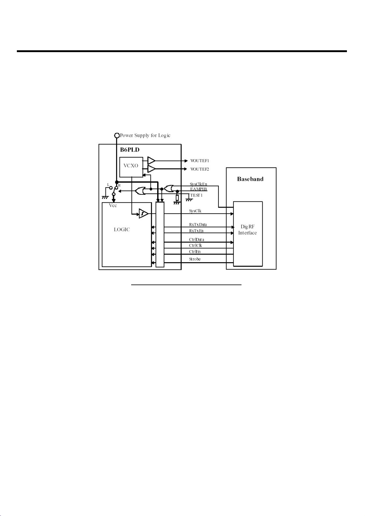
3.2.6 Digital Core
3.2.6.1 Digital Interface Block Diagram
3.2.6.1 Control system and digital interface
The B6PLD is a RF transceiver IC for GSM900, DCS1800 and PCS1900 quad band cellular system,
and incorporates EDGE transceiver capability. The B6PLD has a digital interface connection to the
baseband processor. This interface complies with the digital interface specification DigRF standard
v112.
The digital interface consists of two separate interface connections; (1) the control interface, (2) the
data interface, and a system clock on/off control signal and a precise timing signal. These are
realized by eight signal lines in B6PLD(Look at Fig1.1 above)
-. The control interface is used to configure the B6PLD for RX and TX operation, transfers of control
data for several built-in circuits, and for triggering the events. The control interface comprise a bidirectional 3-wire serial interface with the three signal lines CtrlData, CtrlEn and CtrlClk accessing
the control registers in B6PLD by transferring the control words.
-. The data interface is used to transfer transmit modulation symbols and receive IQ-sampling data.
The data interface comprises a single serial bus with the three signal lines RxTxData, RxTxEn and
SysClk. The SysClk is used for system clock to baseband.
-. The SsClkEn signal enables the SysClk output and powers the 26MHz oscillator on. When the
SysClkEn is negated, the SysClk is held low, and if the TEST1 pin is low by the default settings, the
logic power supply by typical 1.8 volts to the internal core logic circuits is also switched off.
Fig. 1-1 Digital Interface Block Digram

LGE Internal Use Only
Copyright © 2008 LG Electronics. Inc. All right reserved.
Only for training and service purposes
3.3 Digital Baseband
3.3.1 General description
The OMAPV1030 E-GPRS multimedia device belongs to the Texas Instruments OMAP-Vox_
processors family. It combines both a modem engine and an application engine. Memory and CPU
resources are shared between modem and application processing.
The OMAPV1030 chip is based on the OMAP3.4 architecture and integrates two processor
subsystems:
- An MPU subsystem based on an ARM926EJ-S
- A DSP subsystem based on a UMA 2.6 architecture integrating a C55x DSP core
The OMAPV1030’s silicon process technology is a c027.0 90-nm digital CMOS.
3. HW Circuit Description
- 20 -
<Fig.6> OMAPV1030 Block Diagram

LGE Internal Use Only
Copyright © 2008 LG Electronics. Inc. All right reserved.
Only for training and service purposes
3.3.2 Block Description
The OMAPV1030 E-GPRS multimedia device is based on an OMAP3.4 platform that integrates:
- The MPU subsystem
- The DSP subsystem
- A system DMA
- A traffic controller providing:
- External memory interfaces with:
- A slow interface (EMIFS) to ROM, SRAM, FLASH memories
- A fast interface (EMIFF) to SDRAM memories
- Layer 3 (L3) interconnect made of two OCP target ports (OCP-T1 and OCP-T2) and one OCP
initiator port (OCP-I)
- Layer 4 (L4) interconnect made of two DSP peripheral busses (private DSP TIPB and shared DSP
TIPB) and two MPU peripheral busses (public MPU TIPB and private MPU TIPB)
- Clock management
- A set of processor peripherals:
- Three 32-bit timers, a 16-bit Watchdog timer, and an interrupt handler for the MPU
- Three 32-bit timers, a 16-bit Watchdog timer, and a 2nd-level interrupt handler for the DSP
- Test and debug interfaces (JTAG, Window Tracer)
- Trace capabilities: ETM9 and Ctools
The other OMAPV1030 modules or subsystems are connected to the OMAP3.4 platform through the
L3 and L4 interconnects.
3. HW Circuit Description
- 21 -
<Fig.7> OMAPV1030 Top-Level Architecture Overview

LGE Internal Use Only
Copyright © 2008 LG Electronics. Inc. All right reserved.
Only for training and service purposes
The OMAP3.4 platform is the computing core of the device. The other OMAPV1030 components are
organized as follows:
- The internal memory subsystem is made of a single-port 256K-bit shared internal SRAM.
- The security subsystem is a set of several components, including dedicated a secure mode to run
secure applications.
- A master-slave USB module provides an external interface supporting high data transfer rates
between the OMAPV1030 and external application
- The memory interfaces provide access to external memories. There are two types of memory
controllers:
- SDRAM controller supporting SDR and DDR modes
- General-purpose controller supporting asynchronous and synchronous
- The system components are used to manage system interactions such as interrupts, clock control,
reset control, and idle management.
- The peripheral subsystem refers to all the peripherals accessible by the MPU and/or the DSP. They
are all OCP- or TIPB-compliant and are connected to the OMAP3.4 platform through the traffic
controller or the TIPB busses.
3.3.3 RF Interface (Digital RF Interface)
The OMAPV1030 radio interface module of OMAPV1030 device is an interface that carries the
following information:
- Transmit symbols from DBB to RF IC
- Receive samples from RF IC to DBB
- Bidirectional information control
- Real-time and activation signals from DBB to RF IC
- System clock
The OMAPV1030 radio interface module of OMAPV1030 device supports two types of radio
interfaces.
They differ mainly in the type of data interface:
- - The first interface is based on a standard six-wire scheme: three wires for transmit and three for
receive.
- The second one is based on a two-wire bidirectional scheme: one wire for data in/out, and one for
control receive/transmit.
3. HW Circuit Description
- 22 -

LGE Internal Use Only
Copyright © 2008 LG Electronics. Inc. All right reserved.
Only for training and service purposes
This implementation is based on the following:
- The time processing unit (TPU) module is a real-time sequencer dedicated to monitoring GSM
baseband processing.
- The serial port of the time serial port (TSP) module controls both interfaces.
- The real-time TSPACT signal of the TSP module
- The McBSP digital RF module is used for the six-wire data interface.
- The serial radio interface module is used for the two-wire data interface.
- A system clock interface receives a squared 26-MHz clock from the RF IC.
3. HW Circuit Description
- 23 -
<Fig.8> OMAPV1030 Radio Interface
LGE Internal Use Only
Copyright © 2008 LG Electronics. Inc. All right reserved.
Only for training and service purposes
3. HW Circuit Description
- 24 -
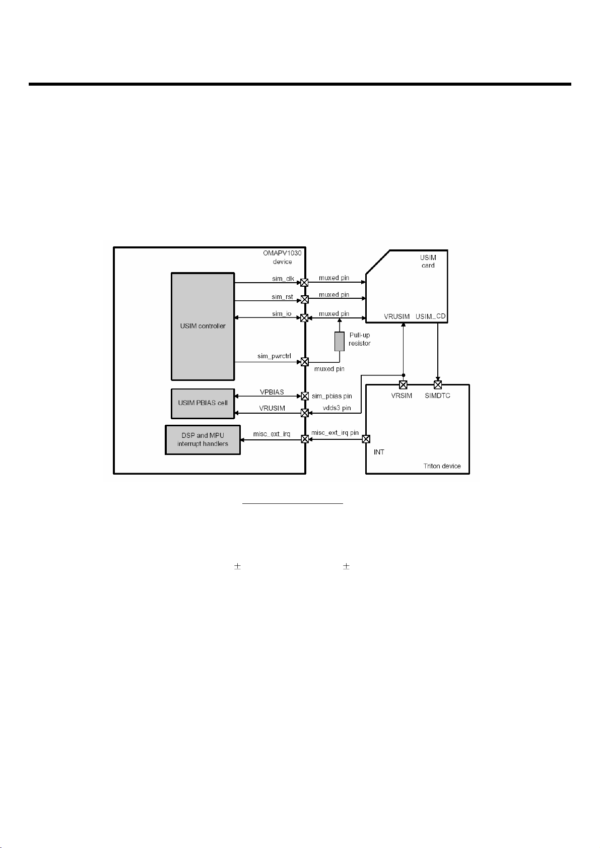
3.3.4 SIM interface
SIM interface scheme is shown in below.
SIM_IO, SIM_CLK, SIM_RST, SIM_PWRCTRL ports are used to communicate DBB via ABB with
plugged sim card and the LDO (VRSIM) in ABB enables operate 1.8V to 2.5V to search SIM card
SIM_CLK: SIM Card reference clock SIM_PWCTRL: SIM Card power activation
SIM_RST: SIM Card async/sync reset SIM_IO: SIM Card bi-directional data line
VRUSIM(Power supply VCC): 3 V 10% (class B) or 1.8 V 10% (class C)
Misc_ext_irq: USIM card presence detection (USIM_CD) purposes.
<Fig.9> SIM Interface
LGE Internal Use Only
Copyright © 2008 LG Electronics. Inc. All right reserved.
Only for training and service purposes
3. HW Circuit Description
- 25 -
3.3.5 UART Interface
KM500D has Three UART Drivers as follow :
- UART1: USB
- UART2: ETM, Calibration
- UART3: AT command, Fax_modem, Bluetooth
UART1(USB)
Resource Name Description
TR_USB_DP DP Data
TR_USB_DM DM Data
USB_PWR POWER USB_POWER
VBUS VBUS USB_Detect
UART2 (ETM)
UART2_RX RX Receive Data(UART2)
UART2_TX TX Transmit Data(UART2)
UART3 (Bluetooth)
UART3_RXD UART3_RXD Receive Data
UART3_TXD UART3_TXD Transmit Data
UART3_RTS UART3_RTS Request To Send
UART3_CTS UART3_CTS Clear To Send
<Table.2> UART Interface Spec

- 26 -
3. HW Circuit Description
3.3.6 GPIO Map
In total 22 allowable resources, KM500D is using 9 resources except 3 resources dedicated to SIM
and Memory. KM500D GPIO(General Purpose Input/Output) Map, describing application, I/O state,
and enable level, is shown in below table 3.
LGE Internal Use Only
Copyright © 2008 LG Electronics. Inc. All right reserved.
Only for training and service purposes
<Table.3> GPIO Map
GPIO No.
gpio_5
gpio_20
gpio_21
gpio_22
gpio_23
ACTIVECOMMENTMode0
LOW HIGHMM RESETMM_RESETgpio_0
-SLIDE UP/DOWN SignalSLIDEgpio_1
LOWCharger IC EnableCHG_ENgpio_2
UART3 DSRUART3_DSR
LOWUSB Download SelectionUSB_BOOT_SELgpio_4
TCC7402Interrupt to hostMM_INT
BB DETECT USBUSB_DETECT_BBgpio_6
TCC7402 BYPASS MODE ENABLEBPENgpio_7
FM Radio Interrupt to HostFM_INTgpio_13
BOOT_SELgpio_17
Neptune Booting Mode Selection(No Bypass
Mode)
USB-CHARGE INTERUPT TO TCC7450USBCHG_INTgpio_26
HS PATH SELECTIONHS_PATH_SELgpio_43
LCD Maker IDLCD_IDgpio_60
FM RESETFM_RESETgpio_63
LO
LOW HIGHLCD RESETLCD_RESET
HIGH:SPEAKERSPEAKER/RECEIVER SelectionSPK_ENgpio_32
HIGH
W HIGHBluetooth ResetBT_NRSTgpio_8
HIGHCAM RECORD SELECTCAM_RECORD_SELgpio_9
HIGHTCC7402 IO ENABLEGATED_IOENgpio_10
HIGHMM 1.2V LDO ENABLEMM_1V2_ENgpio_12
HIGHMAIN KEY BACK LIGHT ENABLEMAIN_KEY_BL_ENgpio_16
PULL-UP
HIGHLCD LDO EnableDP_PWONgpio_18
HIGHMM LDO ENABLEMM_LDO_ENgpio_19
HIGHDAC ENABLEDAC_EN
LOW3.5 PHI JACK DETECTJACK_DETECT_3.5
LOWCharging Indication_CHG_STAT
LOWHOOK DETECTHOOK_DETECTgpio_27
HIGHHOOK ENABLEHOOK_ENgpio_28
HIGHMM USB ENABLEMM_USB_ENgpio_29
HIGHMM 1.5V ENABLEMM_1V5_ENgpio_30
HIGHMP3 BACKLIGHT ENABLEFADEIN_BL_ENgpio_46
LOWJACK DETECTJACK_DETECTgpio_47
HIGHLCD Backlight EnableLCD_BL_ENgpio_59
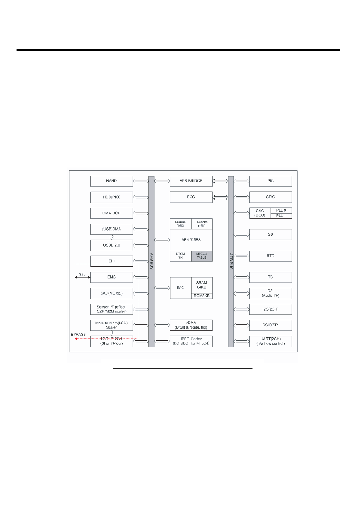
3.4 Multimedia IC
TCC740xA series are system LSI for multimedia application processor based on the ARM946E-S,
ARM’s proprietary 32-bit RISC CPU core. It can decode and encode (M)JPEG, MPEG4, MP3 or
other types of audio / voice / video / image compression / decompression standards by software
based architecture.
The on-chip USB 2.0 compliant controller enables the data transmission between a personal
computer and st orage device such as NAND flash, SD.
- 27 -
3. HW Circuit Description
LGE Internal Use Only
Copyright © 2008 LG Electronics. Inc. All right reserved.
Only for training and service purposes
<Fig.10> Functional Block Diagram of TCC740xA

• General features
ARM946E-S CPU core (16KB instruction/data cache, operating up to 200MHz)
8K bytes of internal boot ROM with various boot procedure (NAND, USB, EHI) and security
64K bytes of internal SRAM for general usage
USB2.0 Device (high, full speed)
I2S interface for external audio
I2C compatible serial bus for audio CODEC & CCD/CMOS sensor control
32-bit 1Hz counter
RTC (Real Time Clock) for battery backup
EHI (External Host Interface) for parallel host interface
Secure Digital Card (SD)
3.4.1 Core
The TCC74x has adopted the ARM946E-S (r1p1) core for controlling system and processing various
kinds of digital signals. The ARM946E-S is a Harvard architecture cached processor with separate
16Kbyte data and 16Kbytes instruction caches, each with 8-word of line length. A protection unit
allows eight regions of memory to be defined, each with individual cache and write buffer
configurations and access permissions. The cache system is software configurable to provide highest
average of performance or to meet the needs of real-time systems.
The followings are key features of the TCC74xx CPU core.
CPU ARM946E-S
Cache 16KB for Data / 16KB for Instruction
TCM 4KB dual port data TCM
3.4.2 USB2.0 Device Controller
The TCC7402 USB2.0 Device supports a fully compliant to USB 2.0 specification, highspeed (480
Mbps) functions and suspend/resume signaling. The USB function controller has an endpoint EP0 for
control, two in/output endpoints EP1/EP2 for bulk data transaction and an EP3 for interrupt data
transaction.
3.4.3 EHI
This LSI has the external host interface (EHI) that allows the external host device to be connected to
the on-chip system bus. The external host device can be directly connected to 68/80-series interfaces
and access the memory area of this LSI. For software based data transfer, EHI can generate the
internal interrupt of this LSI, and this LSI can also send interrupt request to the external host
controller.
LGE Internal Use Only
Copyright © 2008 LG Electronics. Inc. All right reserved.
Only for training and service purposes
3. HW Circuit Description
- 28 -

LGE Internal Use Only
Copyright © 2008 LG Electronics. Inc. All right reserved.
Only for training and service purposes
3. HW Circuit Description
- 29 -
3.4.4 u-SD CONTROLLER
SD/MMC controller is designed to support SD specification Ver.1.01, SDIO specification Ver1.10,
CEATA and MMC specification Ver.3.0. By using DMA and internal FIFO(8x32bits) data transfer rate
is up to maximum speed, SD/MMC card supports. Moreover because this block has internal clock
controller, it is possible to adjust operating frequency for power saving or other operating conditions
just from setting special register.
3.4.5 DAI
The TCC74xx provides digital audio interface that complies with IIS (Inter-IC Sound). The DAI has
five input/output pins for IIS interface; MCLK, BCLK, LRCK, DAI, DAO. All DAI input/output pins are
multiplexed with GPIO pins; GPIO_B<16:20>. The MCLK is the system clock pin that is used for
CODEC system clock. In master mode, the MCLK can be generated from clock generator in which
that is known as a DCLK, or fed from the outside of chip in slave mode. The DAI can process 256fs,
384fs and 512fs as a system clock. 256fs means that the system clock has 256 times of sampling
frequency (fs). The BCLK is the serial bit clock for IIS data exchange. The DAI can generate 64fs,
48fs and 32fs by dividing a system clock. The polarity of BCLK can be programmed. That is, the
serial bit can be stable either rising edge of BCLK or falling edge of BCLK.
The LRCK is the frame clock for the stereo audio channel Left and Right. The frequency of LRCK is
known as the “fs” - sampling frequency. Generally, for audio application - such as MP3 player , CD
player, the fs can be set to 8kHz, 16kHz, 11.05kHz, 24kHz, 32kHz, 44.1kHz and 48kHz. For
supporting the wide range of sampling frequency in audio application, the DCO function is very useful
to generate a system clock. Refer the chapter of clock generator for detail information. All three
clocks (MCLK, BCLK, LRCK) are selectable as master or slave.
The DAI, DAO are the serial data input output pins respectively. The DAI has two 8-word input/output
buffers. It has a banked buffer structure so that one side of buffer is receiving/transmitting data while
the other side of that can be read/written through the DADI_XX/DADO_XX registers. The maximum
data word size is 24 bit. Data is justified to MSB of 32bits and zeros are padded to LSB.
There are 2 types of interrupt from IIS; transmit done interrupt, receive done interrupt. The transmitdone interrupt is generated when the 8 words are transferred successfully in the out put buffer. At this
interrupt, user should fill another 8 more words into the other part of the output buffer in the interrupt
service routine (ISR). In this ISR routine, 8 consecutive stores of word data to the DADO registers are
needed.
The receive-done interrupt is generated when the 8 words are received successfully in the input
buffer. At this interrupt, user should read 8 received words from the input buffer using 8 consecutive
load instructions from the DADI registers.
3.4.6 Camera & LCD
The TCC7402 provides camera interface.
The features of CIF are is 8-bit data and sync line which supports CCIR 601/656, 4:2:2,YCbCr(YUV).
The TCC7402 provides LCD interface. The LCD MODULE of KM500 is 2” TFT-LCD which is
displayed 65000 color. The LCD controller is used to send out image data from the system memory

3.5 Analog Baseband
3.5.1 General Description
The TRITON chip is the analog and power management part of the Texas Instruments next generation
wireless terminal. These GSM/GPRS/E-GPRS, 3G W-CDMA, CDMA2000 platforms are composed of
a digital baseband processor, a RF chip, an application processor OMAP and of different peripheral
devices like a LCD panel, a Multi-Media Card, a Bluetooth modem, a GPS modem.
The purpose of the Triton device is to provide to platforms the following resources:
LGE Internal Use Only
Copyright © 2008 LG Electronics. Inc. All right reserved.
Only for training and service purposes
3. HW Circuit Description
- 30 -
<Fig.11> TWL3029 Architecture
- A power management system
- Power supply resources
- A voice and audio interface
- A battery charger
- A monitoring system
- A real time clock resource
- A USB 2.0 OTG transceiver with a carkit
interface
- Three White-LEDs drivers
- A vibrator driver
- A SIM-Card detection
- A thermal shutdown
- An I2C interface
- A JTAG and boundary scan

3.5.2 Audio Signal Processing & Interface
The Audio module consists of a Voice Codec dedicated to mobile telephone terminal application and a
Stereo path.
- The Voice Codec circuit processes analog audio components in the uplink path and transmits the
converted data to the DSP speech coder through the voice serial port (VSP). In the downlink path,
the Voice Codec converts the digital samples of speech data received from the DSP via the VSP port
into analog audio signals.
The Voice Codec supports a 8kHz (default narrowband mode) to a 16kHz(wideband mode) sampling
frequency.
- The Stereo path converts audio digital samples received from the I2S serial interface into analog
audio. It supports all standard frequencies from 8kHz to 48kHz (8, 11.025, 12, 22.05, 24, 32, 44.1
and 48kHz).
- Two included PLLs provide the suitable system clocks to the Voice and Stereo circuitry (ADC, DACS,
Digital Filters, Digital interfaces). The Audio module supports 3 possible input master clocks: 12MHz,
13MHz and 19.2MHz.
3.5.3 Power Resources
The power supply module of Triton generates the different power supplies required by Triton, the
processors and the external peripherals.
LGE Internal Use Only
Copyright © 2008 LG Electronics. Inc. All right reserved.
Only for training and service purposes
3. HW Circuit Description
- 31 -
 Loading...