

Page 1

Date: April, 2008 / Issue 1.0
Service Manual
Model : KE990/KE990c
Service Manual
KE990/KE990c
Internal Use Only
Page 2

- 3 -
1. INTRODUCTION .............................. 5
1.1 Purpose................................................... 5
1.2 Regulatory Information............................ 5
2. PERFORMANCE...............................7
2.1 Supporting Standard................................7
2.2 Main Parts : Solution................................7
2.3 HW Features............................................8
2.4 HW SPEC. .............................................10
3. TECHNICAL BRIEF ........................15
3.1 General Description ...............................15
3.2 GSM Mode.............................................17
3.3 LO generation and distribution circuits...20
3.4 Off-chip RF Components .......................21
3.5 Digital Baseband (DBB/ESM6270) ........28
3.6 Subsystem(ESM6270)...........................31
3.7 Power Block...........................................38
3.8 External memory interface.....................43
3.9 H/W Sub System....................................45
3.10 Feature List..........................................61
3.11 Multimedia Chip Interface ....................67
3.12 Touch Screen Interface........................73
3.13 Main Features......................................74
3.14 Main Component..................................75
4. TROUBLE SHOOTING ...................81
4.1 RF Component.......................................81
4.2 Main Component....................................82
4.3 Checking VCTCXO Block ......................83
4.4 Checking Front-End Module Block ........85
4.5 Checking GSM Block.............................88
4.6 Power on trouble....................................94
4.7 SIM detect trouble..................................99
4.8 Key sense trouble (KEYPAD) ..............100
4.9 Keypad backlight trouble......................102
4.10 Micro SD trouble ................................104
4.11 Audio trouble......................................105
4.12 Camera trouble ..................................118
4.13 Main LCD trouble...............................121
4.14 Bluetooth trouble................................124
4.15 Touch Screen trouble.........................126
5. DOWNLOAD .................................127
5.1 Introduction ..........................................127
5.2 Downloading Procedure.......................127
5.3 Troubleshooting Download Errors .......142
5.4 Caution.................................................147
6. BLOCK DIAGRAM ........................148
6.1 GSM RF Block .....................................148
6.2 Interface Diagram ................................150
7. Circuit Diagram ............................153
8. BGM Pin Map................................163
9. PCB LAYOUT................................169
10. Calibration & RF Auto Test
Program (Hot Kimchi)................173
10.1 Usage of Hot-Kimchi..........................173
11. EXPLODED VIEW &
REPLACEMENT PART LIST ......177
11.1 EXPLODED VIEW .............................177
11.2 Replacement Parts
<Mechanic component>.....................179
<Main component> ............................183
11.3 Accessory ..........................................203
Table Of Contents
LGE Internal Use Only
Copyright © 2008 LG Electronics. Inc. All right reserved.
Only for training and service purposes
Page 3

- 4 -
LGE Internal Use Only
Copyright © 2008 LG Electronics. Inc. All right reserved.
Only for training and service purposes
Page 4

LGE Internal Use Only
Copyright © 2008 LG Electronics. Inc. All right reserved.
Only for training and service purposes
- 5 -
1.1 Purpose
This manual provides the information necessary to repair, calibration, description and download the
features of this model.
1.2 Regulatory Information
A. Security
Toll fraud, the unauthorized use of telecommunications system by an unauthorized part (for example,
persons other than your company’s employees, agents, subcontractors, or person working on your
company’s behalf) can result in substantial additional charges for your telecommunications services.
System users are responsible for the security of own system.
There are may be risks of toll fraud associated with your telecommunications system. System users
are responsible for programming and configuring the equipment to prevent unauthorized use. The
manufacturer does not warrant that this product is immune from the above case but will prevent
unauthorized use of commoncarrier telecommunication service of facilities accessed through or
connected to it. The manufacturer will not be responsible for any charges that result from such
unauthorized use.
B. Incidence of Harm
If a telephone company determines that the equipment provided to customer is faulty and possibly
causing harm or interruption in service to the telephone network, it should disconnect telephone
service until repair can be done. A telephone company may temporarily disconnect service as long as
repair is not done.
C. Changes in Service
A local telephone company may make changes in its communications facilities or procedure. If these
changes could reasonably be expected to affect the use of the phones or compatibility with the net
work, the telephone company is required to give advanced written notice to the user, allowing the user
to take appropriate steps to maintain telephone service.
D. Maintenance Limitations
Maintenance limitations on the phones must be performed only by the manufacturer or its authorized
agent. The user may not make any changes and/or repairs expect as specifically noted in this manual.
Therefore, note that unauthorized alternations or repair may affect the regulatory status of the system
and may void any remaining warranty.
1. INTRODUCTION
1. INTRODUCTION
Page 5

LGE Internal Use Only
Copyright © 2008 LG Electronics. Inc. All right reserved.
Only for training and service purposes
E. Notice of Radiated Emissions
This model complies with rules regarding radiation and radio frequency emission as defined by local
regulatory agencies. In accordance with these agencies, you may be required to provide information
such as the following to the end user.
F. Pictures
The pictures in this manual are for illustrative purposes only; your actual hardware may look slightly
different.
G. Interference and Attenuation
A phone may interfere with sensitive laboratory equipment, medical equipment, etc. Interference from
unsuppressed engines or electric motors may cause problems.
H. Electrostatic Sensitive Devices
ATTENTION
Boards, which contain Electrostatic Sensitive Device (ESD), are indicated by the sign.
Following information is ESD handling:
• Service personnel should ground themselves by using a wrist strap when exchange system boards.
• When repairs are made to a system board, they should spread the floor with anti-static mat which is
also grounded.
• Use a suitable, grounded soldering iron.
• Keep sensitive parts in these protective packages until these are used.
• When returning system boards or parts like EEPROM to the factory, use the protective package as
described.
1. INTRODUCTION
- 6 -
Page 6

LGE Internal Use Only
Copyright © 2008 LG Electronics. Inc. All right reserved.
Only for training and service purposes
2. PERFORMANCE
- 7 -
2.1 Supporting Standard
2.2 Main Parts : GSM Solution
2. PERFORMANCE
Item Feature Comment
Supporting Standard GSM900/DCS1800/PCS1900
with seamless handover
Phase 2+(include AMR)
SIM Toolkit : Class 1, 2, 3, A-E
Frequency Range GSM900 TX : 880 - 915 MHz
GSM900 RX : 925 - 960 MHz
DCS1800 TX : 1710 - 1785 MHz
DCS1800 RX : 1805 - 1880 MHz
PCS1900 TX : 1850 - 1910 MHz
PCS1900 RX : 1930 - 1990 MHz
Application Standard WAP 2.0, JAVA 2.0
Item Part Name Comment
Digital Baseband Neptune (D761811BZVL): TI
Analog Baseband Triton (TWL3029): TI
RF Chip RTR6235 : Qualcomm
Page 7

LGE Internal Use Only
Copyright © 2008 LG Electronics. Inc. All right reserved.
Only for training and service purposes
2.3 HW Features
2. PERFORMANCE
- 8 -
Item Feature Comment
Form Factor Slide
Battery 1) Capacity
Standard : Li-Ion, 800mAh
2) Packing Type : Soft Pack
Size Standard : 100.4 X 48.0 X 14.5 mm
Weight TBD With Battery
Volume 70cc
PCB Staggered 8Layers , 0.8t
Stand by time 250 hrs @ Paging Period 9
Charging time 3 hrs @ Power Off / 800mAh
Talk time Min : 3.0 hrs @ Power Level 7 @ GSM850 / 800mAh
RX sensitivity GSM900 : -105 dBm
DCS 1800 : -105 dBm
PCS 1900 : -105 dBm
GSM900 : 33 dBm Class4 (GSM900)
DCS 1800 : 30 dBm Class1 (PCS)
PCS 1900 : 30 dBm Class1 (DCS)
GSM900 : 27 dBm E2 (GSM900)
DCS 1800 : 26 dBm E2 (PCS)
PCS 1900 : 26 dBm E2 (DCS)
GPRS compatibility GPRS Class 12
EDGE compatibility EDGE Class 12
SIM card type Plug-In SIM
3V /1.8V
Display Main LCD
262K Color TFT (320 x 240)
Backlight : White LED
Built-in Camera 2M CMOS Camera (VGA) One button access
Status Indicator None
TX output
power
GSM/
GPRS
EDGE
Page 8

LGE Internal Use Only
Copyright © 2008 LG Electronics. Inc. All right reserved.
Only for training and service purposes
2. PERFORMANCE
- 9 -
Item Feature Comment
Keypad Alphanumeric Key : 12 Function Key:
Function Key : 14 4 Key Navigation, OK, F1,
Side Key : 4 F2, CLR, SND, MOD
Total No of Keys :30 Side Key : Volume up/down,
CAM, PWR/END
ANT Main : Internal Fixed Type
System connector 18 Pin
Ear Phone Jack 18pin, 4 Pole, Stereo
PC synchronization Yes
Memory NAND Flash : 1Gbit
SDRAM : 512Mbit
Speech coding FR, EFR, HR,AMR
Data & Fax Built in Data & Fax support
Vibrator Built in Vibrator
Blue Tooth V1.2, A2DP,
MIDI(for Buzzer Function) SW Decoded 40Poly
Music Player MP3/ WMA/AAC/HE-AAC/EAAC+ With Graphic EQ
Video Player MPEG4, H.263, WMV9
Camcorder MPEG4, H.263,
Voice Recording Yes
Speaker Phone mode Yes
Support
Travel Adapter Yes
CDROM Yes
Stereo Headset Yes Optional
Data Cable Yes Optional
T-Flash Yes Optional
(External Memory)
Page 9

LGE Internal Use Only
Copyright © 2008 LG Electronics. Inc. All right reserved.
Only for training and service purposes
2. PERFORMANCE
- 10 -
2.4 HW SPEC.
Item Description Specification
1Frequency Band GSM
TX: 890 + 0.2 x n MHz
RX: 935 + 0.2 x n MHz ( n = 1 ~ 124 )
EGSM
TX: 890 + 0.2 x (n-1024) MHz
RX: 935 + 0.2 x (n-1024) MHz ( n = 975 ~ 1023 )
DCS1800
TX: 1710.2 + 0.2 x (n-512) MHz
RX: 1805.2 + 0.2 x (n-512) MHz (n = 512 ~ 885)
PCS1900
TX: 1850 + ( n-511 ) x 0.2 MHz
RX: 1930 + ( n-511 ) x 0.2 MHz (n = 512 ~ 810)
2 Phase Error RMS < 5 degrees
Peak < 20 degrees
3 Frequency Error < 0.1ppm
4 Power Level GSM, EGSM
Level Power Toler. Level Power Toler.
5 33 dBm 2dB 13 17 dBm 3dB
6 31 dBm 3dB 14 15 dBm 3dB
7 29 dBm 3dB 15 13 dBm 3dB
8 27 dBm 3dB 16 11 dBm 5dB
9 25 dBm 3dB 17 9 dBm 5dB
10 23 dBm 3dB 18 7 dBm 5dB
11 21 dBm 3dB 19 5 dBm 5dB
12 19 dBm 3dB
DCS / PCS
Level Power Toler. Level Power Toler.
0 30 dBm 2dB 8 14 dBm 3dB
1 28 dBm 3dB 9 12 dBm 4dB
2 26 dBm 3dB 10 10 dBm 4dB
3 24 dBm 3dB 11 8 dBm 4dB
4 22 dBm 3dB 12 6 dBm 4dB
5 20 dBm 3dB 13 4 dBm 4dB
6 18 dBm 3dB 14 2 dBm 5dB
7 16 dBm 3dB 15 0 dBm 5dB
Page 10

LGE Internal Use Only
Copyright © 2008 LG Electronics. Inc. All right reserved.
Only for training and service purposes
2. PERFORMANCE
- 11 -
Item Description Specification
5 Output RF Spectrum GSM, EGSM
(due to modulation) Offset from Carrier (kHz). Max. dBc
100 +0.5
200 -30
250 -33
400 -60
600 ~ 1,200 -60
1,200 ~ 1,800 -60
1,800 ~ 3,000 -63
3,000 ~ 6,000 -65
6,000 -71
DCS / PCS
Offset from Carrier (kHz). Max. dBc
100 +0.5
200 -30
250 -33
400 -60
600 ~ 1,200 -60
1,200 ~ 1,800 -60
1,800 ~ 3,000 -65
3,000 ~ 6,000 -65
6,000 -73
6 Output RF Spectrum GSM, EGSM
(due to switching transient) Offset from Carrier (kHz) Max. (dBm)
400 -19
600 -21
1,200 -21
1,800 -24
Page 11

LGE Internal Use Only
Copyright © 2008 LG Electronics. Inc. All right reserved.
Only for training and service purposes
2. PERFORMANCE
- 12 -
Item Description Specification
6 Output RF Spectrum DCS / PCS
(due to switching transient) Offset from Carrier (kHz). Max. (dBm)
400 -22
600 -24
1,200 -24
1,800 -27
7 Spurious Emissions Conduction, Emission Status
GSM, EGSM
8Bit Error Ratio
BER (Class II) < 2.439% @-102dBm
DCS / PCS
BER (Class II) < 2.439% @-102dBm
9 Rx Level Report accuracy
10 SLR 8 3 dB
Frequency (Hz) Max.(dB) Min.(dB)
100 -12 200 0 300 0 -12
11 Sending Response 1,000 0 -6
2,000 4 -6
3,000 4 -6
3,400 4 -9
4,000 0 -
12 RLR 2 3 dB
Frequency (Hz) Max.(dB) Min.(dB)
100 -12 200 0 300 2 -7
500
*
-5
13 Receiving Response 1,000 0 -5
3,000 2 -5
3,400 2 -10
4,000 2
*
Mean that Adopt a straight line in between 300 Hz
and 1,000 Hz to be Max. level in the range.
Page 12

LGE Internal Use Only
Copyright © 2008 LG Electronics. Inc. All right reserved.
Only for training and service purposes
2. PERFORMANCE
- 13 -
Item Description Specification
14 STMR 13 5 dB
15 Stability Margin > 6 dB
16 Distortion dB to ARL (dB) Level Ratio (dB)
-35 17.5
-30 22.5
-20 30.7
-10 33.3
0 33.7
7 31.7
10 25.5
17 Side Tone Distortion Three stage distortion < 10%
18
<Change> System frequency 2.5ppm
(13 MHz) tolerance
19 <Change>32.768KHz tolerance 30ppm
20 Power consumption Full power : < 340mA (GSM850) ; < 260mA (DCS / PCS)
Standby : - Normal Mode 4.0mA(Max. power)
- Using Test mode on DSP Sleep function 6mA
21 Talk Time GSM850/Level7 (Battery 800mA):210 Min
GSM850/Level12(Battery 800mA):350 Min
PCS1900/Level5 (Battery 800mA):310 Min
PCS1900/Level10(Battery 800mA):390 Min
22 Standby Time Under conditions, at least 200 hours: Brand new and full
800mAh battery Full charge, no receive/send and keep GSM
in idle mode. Broadcast set off. Signal strength display
labove. Backlight of phone set off.
23 Ringer Volume At least 80 dB under below conditions:
1. Ringer set as ringer.
2. Test distance set as 50 cm
24 Charge Voltage Fast Charge : < 600 mA
Slow Charge: < 60 mA
25 Antenna Display Antenna Bar Number Power
4-90 dBm ~ -86 dBm
3-95 dBm ~ -91 dBm
2-100 dBm ~ -96 dBm
1-105 dBm ~ -101 dBm
0~ -105 dBm
Page 13

Item Description Specification
26 Battery Indicator Battery Bar Number Voltage
0(included Blinking) 3.65V ~ 3.35V
1 3.71V ~ 3.66V
2 3.78V ~ 3.72V
3 3.91V ~ 3.79V
4 4.20V ~ 3.92V
27 Low Voltage Warning 3.5 0.03 V (Call)
3.6 0.03 V (Standby)
28 Forced shut down Voltage 3.35 0.03 V
29 Battery Type 1 Li-Ion Battery
Standard Voltage = 3.7 V
Battery full charge voltage = 4.2 V
Capacity: Min 930mAh
30 Travel Charger Switching-mode charger
Input: 100 ~ 240 V, 50/60Hz
Out put: 5.1V, 700mA
LGE Internal Use Only
Copyright © 2008 LG Electronics. Inc. All right reserved.
Only for training and service purposes
2. PERFORMANCE
- 14 -
Page 14
LGE Internal Use Only
Copyright © 2008 LG Electronics. Inc. All right reserved.
Only for training and service purposes
3. TECHNICAL BRIEF
- 15 -
3.1 General Description
The KE990/KE990c supports EGSM-900, DCS-1800, and PCS-1900 based GSM/GPRS/EDGE. All
receivers and transmitter use the radioOne 1Zero-IF architecture to eliminate intermediate
frequencies, directly converting signals between RF and baseband. The quad-band GSM transmitters
use a baseband-to-IF upconversion followed by an offset phase-locked loop that translates the
GMSKmodulated or 8-PSK-modulated signal to RF.
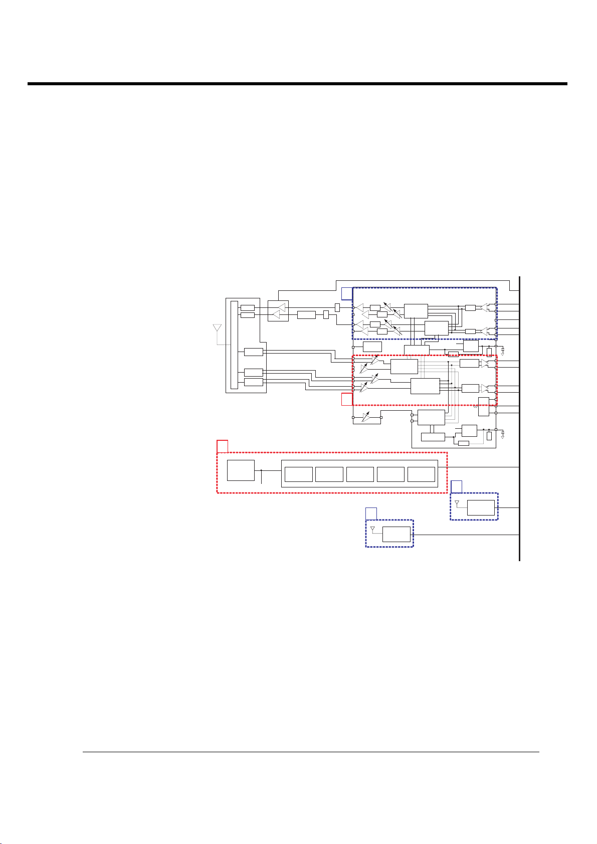
A generic, high-level functional block diagram of KE990/KE990c is shown in Figure 3-1. One antenna
collects base station forward link signals and radiates handset reverse link signals. The antenna
connects with receive and transmit paths through a FEM(Front End Module).
3. TECHNICAL BRIEF
[Fig 3.1] Block diagram of RF part
1
QUALCOMM’s branded chipset that implements a Zero-IF radio architecture.
GESM/ DCS1800/
PCS1900
1. RTR6235 for GSM/EDGE Tx
2. RTR6235 for GSM/EDGE Rx
3. PM6635-3P for Power
Management
4. FM radio Module
5. Bluetooth RF Module
1
H-BPF
L-BPF
SW
GSM850
F
Rx BP
GSM1800
Rx BPF
GSM1900
Rx BPF
GSM/EDGE PA
Tx BPF
G900
pad
pad
Power
Detector
BPF
BPF
BPF
BPF
LO generation
Quadrature
Downconverter
Quadrature
Upconverter
& Distr ibution
Quadrature
Downconverter
Quadrature
Upconverte
2
Quadrature
Downconverter
LPF & DC
Correction
3
Phone
VCTCX
O
RTR6275_TCXO
PM6635-3P
Input Power
Management
Voltage
Regulators
General
Housekeeping
User
InterfacesICInterfaces
5
Bluetooth
e
Modul
LPF
DAC_REF
r
LPF
f
F re
PLL #1
VCO
LPF & DC
Correction
LPF & DC
Correction
Ctls
F ref
PLL #2
VCO
RTR6275_TCXO
F ref
LPF
VDDM
s
& cont rol
Dugital IO s
LPF
MSM_TCXO
ESM6270
4
FM Radio
Module
Page 15

LGE Internal Use Only
Copyright © 2008 LG Electronics. Inc. All right reserved.
Only for training and service purposes
In the GSM receive path, the received RF signals are applied through their bandpass filters and downconverted directly to baseband in the RTR6235 transceiver IC.
These baseband outputs are routed to the ESM IC for further signal processing.
The GSM/EDGE transmit path employs one stage of up-conversion and, in order to improve efficiency,
is divided into phase and amplitude components to produce an open-loop Polar topology:
1. The on-chip quadrature up-converter translates the GMSK-modulated signal or 8- PSK modulated
signal, to a constant envelope phase signal at RF;
2. The amplitude-modulated (AM) component is applied to the ramping control pin of Polar power
amplifier from a DAC within the ESM
KE990/KE990c power supply voltages are managed and regulated by the PM6635 Power
Management IC. This versatile device integrates all wireless handset power management, general
housekeeping, and user interface support functions into a single mixed signal IC. It monitors and
controls the external power source and coordinates battery recharging while maintaining the handset
supply voltages using low dropout, programmable regulators.
The device’s general housekeeping functions include an ADC and analog multiplexer circuit for
monitoring on-chip voltage sources, charging status, and current flow, as well as user-defined off-chip
variables such as temperature, RF output power, and battery ID. Various oscillator, clock, and counter
circuits support IC and higher-level handset functions. Key parameters such as under-voltage lockout
and crystal oscillator signal presence are monitored to protect against detrimental conditions.
3. TECHNICAL BRIEF
- 16 -
Page 16

3.2 GSM Mode
3.2.1 GSM Receiver
The Dual-mode KE990/KE990c’s receiver functions are split between the three RFICs as follows:
■ EGSM-900, DCS-1800 and PCS-1900 modes both use the RTR6235 IC only.Each mode has
independent front-end circuits and down-converters, but they share common baseband circuits (with
only one mode active at a time). All receiver control functions are beginning with SBI2-controlled
parameters.
RF Front end consists of antenna, antenna switch module (LMSP43QA-538) which includes four RX
saw filters (EGSM-900, DCS-1800 and PCS-1900). The antenna switch module allows multiple
operating bands and modes to share the same antenna. In KE990/KE990c, a common antenna
connects to one of six paths: 1) GSM 900 Tx (Low Band Tx’s share the same path), 2) GSM1800/1900
Tx (High Band Tx’s share the same path), 3) EGSM900 Rx, 4) GSM1800 Rx, 5) GSM1900 Rx.
EGSM900, DCS1800, and PCS1900 operation is time division duplexed, so only the receiver or
transmitter is active at any time and a frequency duplexer is not required.
The EGSM900, DCS1800, and PCS1900 receiver inputs of RTR6235 are connected directly to the
transceiver front-end circuits(filters and antenna switch module).
EGSM900, DCS1800, and PCS1900 receiver inputs use differential configurations to improve
common-mode rejection and second-order non-linearity performance. The balance between the
complementary signals is critical and must be maintained from the RF filter outputs all the way into the
IC pins.
Since EGSM900, DCS1800, and PCS1900 signals are time-division duplex (the handset can only
receive or transmit at one time), switches are used to separate Rx and Tx signals in place of frequency
duplexers - this is accomplished in the switch module.
2
The RFIC operating modes and circuit parameters are ESM-controlled through the proprietary 3-line Serial Bus Interface (SBI). The Application
Programming Interface (API) is used to implement SBI commands. The API is documented in AMSS Software - please see applicable AMSS
Software documentation for details.
LGE Internal Use Only
Copyright © 2008 LG Electronics. Inc. All right reserved.
Only for training and service purposes
3. TECHNICAL BRIEF
- 17 -
[Table 3.2.1] Antenna Switch Module Control logic
Page 17

LGE Internal Use Only
Copyright © 2008 LG Electronics. Inc. All right reserved.
Only for training and service purposes
The EGSM900, DCS1800, and PCS1900 receive signals are routed to the RTR6235 through band
selection filters and matching networks that transform single-ended 50-Ω•sources to differential
impedances optimized for gain and noise figure. The RTR input uses a differential configuration to
improve second-order inter-modulation and common mode rejection performance. The RTR6235 input
stages include ESMcontrolled gain adjustments that maximize receiver dynamic range.
The amplifier outputs drive the RF ports of the quadrature RF-to-baseband downconverters. The
downconverted baseband outputs are multiplexed and routed to lowpass filters (one I and one Q)
having passband and stopband characteristics suitable for GMSK or 8-PSK processing. These filter
circuits include DC offset corrections. The filter outputs are buffered and passed on to the ESM6270 IC
for further processing
3. TECHNICAL BRIEF
- 18 -
[Fig 3.2.2] RTR6235 RX feature
Page 18

LGE Internal Use Only
Copyright © 2008 LG Electronics. Inc. All right reserved.
Only for training and service purposes
3. TECHNICAL BRIEF
- 19 -
3.2.2 GSM Transmitter
The RTR6235 transmitter outputs(DA_HB2_OUT and DA_LB1_OUT) include on-chip output matching
inductors. 50ohm output impedance is achieved by adding a series capacitor at the output pins. The
capacitor value may be optimized for specific applications and PCB characteristics based on pass-band
symmetry about the band center frequency, the suggested starting value is shown in Figure3.2.3.
The RTR6235 IC is able to support GSM 850/900 and GSM 1800/1900 mode transmitting. This design
guideline shows a Quad-band GSM application.
Both high-band and low band outputs are followed by resistive pads to ensure that the load Presented
to the outputs remains close to 50ohm. The low-band GSM. Tx path also includes a Tx-band SAW filter
to remove noise-spurious components and noise that would be amplified by the PA and appear in the
GSM Rx band
[Fig 1.3] GSM Transmitter matching
6pF
DA_HB2_OUT
68
HB_IN
91 91
HB_OUT
RTR6235 GSM PA
5pF
DA_LB1_OUT
51
Tx
SAW
120 120
LB_IN
LB_OUT
Page 19

LGE Internal Use Only
Copyright © 2008 LG Electronics. Inc. All right reserved.
Only for training and service purposes
3.3 LO generation and distribution circuits
The integrated LO generation and distribution circuits are driven by internal VCOs to support various
modes to yield highly flexible quadrature LO outputs that drive all GSM/EDGE band upconverters and
downconverters; with the help of these LO generation and distribution circuits, true zero-IF architecture
is employed in all GSM band receivers and transmitters to translate the signal directly from RF to
baseband and from baseband to RF.
Two fully functional fractional-N synthesizers, including VCOs and loop filters, are integrated within the
RTR6235 IC. The synthesizer (PLL1) creates the transceiver LOs that support four GSM band
receivers and transmitters including: GSM850, EGSM900, DCS1800, and PCS1900. An external
TCXO input signal is required to provide the synthesizer frequency reference to which the PLL is
phase and frequency locked. The RTR6235 IC integrates most of PLL loop filter components on-chip
except two off-chip loop filter series capacitors, and significantly reduces off-chip component
requirement. With the integrated fractional-N PLL synthesizers, the RTR6235 has the advantages of
more flexible loop bandwidth control, fast lock time, and low-integrated phase error
3. TECHNICAL BRIEF
- 20 -
Page 20

LGE Internal Use Only
Copyright © 2008 LG Electronics. Inc. All right reserved.
Only for training and service purposes
3. TECHNICAL BRIEF
- 21 -
3.4 Off-chip RF Components
3.4.1 VCTCXO (X100 : TG-5010LH(19.2M))
The Voltage Controlled Temperature Compensated Crystal Oscillator (VCTCXO) provides the
reference frequency for all RFIC synthesizers as well as clock generation functions within the
ESM6270 IC. The oscillator frequency is controlled by the ESM6270 IC.s TRK_LO_ADJ pulse density
modulated signal in the same manner as the transmit gain control TX_AGC_ADJ. A two-pole RC
lowpass filter is recommended on this control line.
The PM6635 IC controls the handset power-up sequence, including a special VCTCXO warm-up
interval before other circuits are turned on. This warm-up interval (as well as other TCXO controller
functions) is enabled by the ESM TCXO_EN line . The PM6635 IC VREG_TCXO regulated output
voltage is used to power the VCTCXO and is enabled before most other regulated outputs.
Any GSM mode power control circuits within the ESM6270 IC require a reference voltage for proper
operation and sufficient accuracy. Connecting the PM6635 IC REF_OUT directly to the ESM6270 IC
GSM_PA_PWR_CTL_REF provides this reference. This sensitive analog signal needs a 0.1 •ÏF low
frequency filter near to ESM side, and isolate from digital logic and clock traces with ground on both
sides, plus ground above and below if routed on internal layers.
3.4.2 Front-End Module (FL100 : LMSP43QA-538)
This equipment uses a single antenna to support all handset operating modes, with an antenna switch
module select the operating frequency and band. The active connection is ESM-selected by three
control lines (GPIO[9] and GPIO[10]). These GPIOs are programmed to be ANT_SEL0 and
ANT_SEL1 respectively.
[Table 3.4.2] Front End Module control logic
Page 21

LGE Internal Use Only
Copyright © 2008 LG Electronics. Inc. All right reserved.
Only for training and service purposes
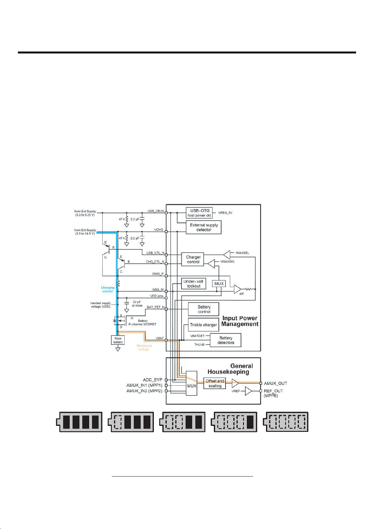
3.4.3 PMIC Functional Block Diagram (U501 : PM6635-3P)
■ Input power management
- Valid external supply attachment and removal detection
- Supports unregulated (closed-loop) external charger supplies and USB supplies as input power
sources
- Supports lithium-ion main batteries
- Trickle, constant current, constant voltage, and pulsed charging of the main battery
- Supports coin cell backup battery (including charging)
- Battery voltage detectors with programmable thresholds
- VDD collapse protection
- Charger current regulation and real-time monitoring for over-current protection
- Charger transistor protection by power limit control
- Control drivers for two external pass transistors and one external battery MOSFET - MOSFET is
optional
- Voltage, current, and power control loops
- Automated recovery from sudden momentary power loss
■ Output voltage regulation
- One boost (step-up) switched-mode power supply (SMPS) for driving white LEDs and hosting
USBOTG
- Three buck (step-down) switched-mode power supplies that efficiently generate ESMC, ESME,
and PA (or second ESMC) supply voltages
- Supports dynamic voltage scaling (DVS) for ESMC and PA
- Eleven low dropout regulator circuits with programmable output voltages, implemented using three
different current ratings: 300 mA (two), 150 mA (six), and 50 mA (three). These can be used to
power ESMA, ESMP, RFRX1, RFRX2, RFTX, SYNT, TCXO, WLAN, MMC, USB, and RUIM
circuits.
- All regulators can be individually enabled/disabled for power savings
- Low power mode available on ESMA and ESMP regulators
- All regulated outputs are derived from a common bandgap reference - close tracking
3. TECHNICAL BRIEF
- 22 -
Page 22

LGE Internal Use Only
Copyright © 2008 LG Electronics. Inc. All right reserved.
Only for training and service purposes
■ Integrated handset-level housekeeping functions reduces external parts count, size, cost
- Analog multiplexer selects from 8 internal and up to 18 external inputs
- Multiplexer output’s offset and gain are adjusted, increasing the effective ADC resolution
- Adjusted multiplexer output is buffered and routed to an ESM device ADC
- Dual oscillators - 32.768 kHz off-chip crystal and on-chip RC assures ESM device sleep clock
- Crystal oscillator detector and automated switch-over upon lost oscillation
- Real time clock for tracking time and generating associated alarms
- On-chip adjustments minimize crystal oscillator frequency errors
- Circuits control TCXO warm-up and synchronize, deglitch, and buffer the TCXO signal
- TCXO buffer control for optimal QPH/catnap timing
- Three-stage over-temperature protection (smart thermal control)
■ Integrated handset-level user interfaces
- Four programmable current sinks recommended as keypad backlight, LCD backlight, camera
flash, and general-purpose drivers
- Vibration motor driver programmable from 1.2 to 3.1V in 100 mV increments
- Speaker driver with programmable gain, turn-on time, and muting; differential operation (drives
external 8 Ω speakers with volume controlled 500 mW)
■ IC-level interfaces
- ESM device-compatible 3-line SBI for efficient initialization, status, and control
- Supports the ESM device’s interrupt processing with an internal interrupt manager
- Many functions monitored and reported through real-time and interrupt status signals
- Dedicated circuits for controlled power-on sequencing, including the ESM device’s reset signal
- Several events continuously monitored for triggering power-on/power-off sequences
- Supports and orchestrates soft resets
- USB-OTG transceiver for full-speed (12 Mb/s) and low speed (1.5 Mb/s) interfacing of the ESM
device to computers as a USB peripheral, or connecting the ESM device to other peripherals
- RUIM level translators enable ESM device interfacing with external modules
■ Twelve multi-purpose pins that can be configured as digital or analog I/Os, bidirectional I/Os, or
current sinks. Default functions support the RUIM level translators, power-on circuits, analog
multiplexer inputs, an LED driver, and a reference voltage buffer.
■ Highly integrated functionality in a small package - 84-pin BCCS with a large center slug for
electrical ground, mechanical stability, and thermal relief
3. TECHNICAL BRIEF
- 23 -
Page 23

LGE Internal Use Only
Copyright © 2008 LG Electronics. Inc. All right reserved.
Only for training and service purposes
3. TECHNICAL BRIEF
- 24 -
[Figure 3.4.3] PM6635 Block Diagram
Page 24

LGE Internal Use Only
Copyright © 2008 LG Electronics. Inc. All right reserved.
Only for training and service purposes
3. TECHNICAL BRIEF
- 25 -
3.4.4 GSM PAM (U101:TQM7M5003)
The TQM7M5003 is an extremely small (7 x 7 mm), GSM/EDGE PAM for handset applications. This
module has been optimized for excellent EDGE efficiency and Pout in a Polar Loop environment at
EDGE class E2+ operation while maintaining high GSM/GPRS efficiency.
The small size and high performance is achieved with high-reliability 3 rdgeneration InGaP HBT
technology. With 50Ω and output, no external matching or bias components are required. The module
incorporates two highly-integrated InGaP power amplifier die with a CMOS controller. Each amplifier
has three gain stages with on-die inter-stage matching implemented with a high Q passives technology
for optimal performance. The CMOS controller implements a fully integrated power control within the
module for GSM operations, and serves as the AM/AM path in EDGE operations. This eliminates the
need for any external couplers, power detectors, current sensing etc., to assure the output power level.
The module has Tx enable and band select inputs. Module construction is a low-profile overmolded
landgrid array on laminate.
[Figure 3.4.4] GSM PAM Schematic
L112
15nH
C146 2.7p
C142
5.6nH
14
GND6
13
GND5
12
VCC
GND4
GND3
GSM_OUT
GND2
U101
TQM7M5003
GND7
GND8
17
16
6.8pC136
C138
NA
L113
5.6nH
11
10
9
8
DCS_PCS_IN
TX_EN
VBATT
GND1
VRAMP
DCS_PCS_OUT
GSM_IN
15
1
2
BS
3
4
5
6
7
R117 2.2K
C143
68p
GSM_PA_BAND MODE
LOW
HIGH
C137
1u
GSM850/900
DCS/PCS
GSM_PA_BAND
GSM_PA_EN
C135
33u
GSM_PA_RAMP
+VPWR
EFCH836MTDB1
FL101
3
G12G2
IN
1
G3
O1
5
4
R112
R111
68
10 dB
100
R114
68
R118
100
10dB
R113
R119
100
DCS_PCS_TX
100
GSM_TX
Page 25

- 26 -
3. TECHNICAL BRIEF
LGE Internal Use Only
Copyright © 2008 LG Electronics. Inc. All right reserved.
Only for training and service purposes
3.4.5 Bluetooth (M800 : LBRQ-2B43A)
The ESM6270 includes BT baseband embedded BT 1.1 compliant baseband core, so the other
bluetooth components are bluetooth RF module and Antenna.
Figure3.4.5 shows the bluetooth system architecture in the KE990/KE990c.
A
[Figure 3.4.5] Bluetooth system architecture
ESM 6270
Bluetooth Baseband
rt
BT_TX _RX_N
SBST
BT_DA TA
SBC K
SBD T
BT_CLK
NT
LB RQ-2B43A
SY N C_ D E T / TX _E N
RX_BB/TX _BB
BPF
16
BCM2004
CLK_REF
SBST
SBC K
SBD T
BlueQ I nterface Pa
5
4
13
11
12
Clo ck Part
9
7
LDO Part
GND Part
GND
1 2 3
678
15
VDD_I NT
VCC_OUT
XTAL_IN
VD D_M SM
VD D_BAT
Supply Part
10
14
TCXO
VR EG_M SM P
A
VD D_
Page 26

- 27 -
3. TECHNICAL BRIEF
LGE Internal Use Only
Copyright © 2008 LG Electronics. Inc. All right reserved.
Only for training and service purposes
3.4.6 FM Radio (U103 : TEA5766UK)
This FM Module is a single chip, electronically tuned, FM stereo radio with RDS/RBDS demodulator
and decoder for low voltage applications, with fully integrated IF selectivity and demodulation. This
equipment tunes the European, US, and Japanese FM bands. Figure3.4.6 shows the FM Radio
system architecture in the KE990.
[Figure 3.4.6]
To MM I
From MM I
Headphon e
MAX9722B ET
To SPEAK ER
AMP
FM_AN
T
RFIN1
RFIN
HP_EAR_R/LMIDI_EAR_R/L
E
SPK_OUT+/-
2
FM Radio
TEA5766 UK
Philip
s
Audio Codec
32. 768KH z
N
FREQI
BUSE
N
INT
X
CLOCK
DATA
VAF R
VAF L
WM8983
From PMIC
FM_AUDIO_R/L
HP_SPK_R/L
GRFC 3_GPIO 6
GRFC 4_AU X_SBC K_GPIO 7
I2C_SC L_GPIO27
I2C_SD A_GPIO26
ESM6270
Page 27

LGE Internal Use Only
Copyright © 2008 LG Electronics. Inc. All right reserved.
Only for training and service purposes
3. TECHNICAL BRIEF
- 28 -
3.5 Digital Baseband (DBB/ESM6270)
3.5.1 General Description
A. Features (ESM6270)
■ Support for multimode operation - GSM/GPRS/EDGE, and GPS
■ High-performance ARM926EJ-S¢‚ running at up 270 MHz
■ ARM Jazelle Java hardware acceleration for faster Java-based games and other applets
■ QDSP4000 high-performance DSP cores
■ Integrated gpsOne position location technology functionality
■ Integrated Bluetooth 1.2 baseband processor for wireless connectivity to peripherals
■ Qcamera¢‚ with 30 fps QVGA viewfinder resolution, and support for 4 MP camera sensors
■ Direct interface to digital camera module with video front-end (VFE) image processing
■ True 3D graphics for advanced wireless gaming
■ SecureMSM v2.0 includes support for SIM-lock and IMEI integrity, and Qfuse
■ Audio on par with portable music players
■ Vocoder support (AMR, FR, EFR, HR)
■ Advanced 14 x 14 mm, 0.5 mm pitch, 409-pin lead-free CSP technology
■ SD/SDIO hardware support
Page 28

LGE Internal Use Only
Copyright © 2008 LG Electronics. Inc. All right reserved.
Only for training and service purposes
3. TECHNICAL BRIEF
- 29 -
From CAM_MIC
Figure. Simplified Block Diagram of Baseband
CAM_MIC+
EAR_MIC_P
From MMI
From PMIC
From TOUCH WINDOW
From PMIC
MIDI_EAR_L
Headphone
MIDI_EAR_RTo MMI
MAX9722BETE
MIDI_3.3VFrom LDO
VREG_MSMP_2.7V / VREG_ MMC_3.0V
X+/-
Y+/-
LCD_ VDD_2.8VFrom LDO
Anal og
S/W
NC7SB 3157
EAR_SENSE_NVREG_MSMP_2.7V
AMP
HP_ AMP_EN From ESM
SLEEP_CLK
From PMIC
VREG_MSMP_2.7V
TOSHIBA 2G/1G
TYA000BC00HOG
Touch D river
TSC2007IYZGR
MIDI_MICP
From ESM
HP_ EAR_L
HP_EAR_ R
AUDIO CODEC
SPK_ OUT+
SPK_ OUT-To MODULE SPEAKER
From LDO
MIDI_3.3V
MOTOR+
MOTOR-To M OTOR
VREG_MMC_3.0VFrom PMIC LIN_ MOTOR_EN From ESM
FM_ANTFrom MMI
From PMIC
VREG_ MSME_1.8V
MCP
From FM RADIO
WM8983
VREG_WM_2.7V
VREG_MSME_1.8V
Linear M otor Dri ver
To RECEIVER
FM RADIO
TEA57 66UK
VREG_5V
MIC
EBI2_DA TA[0:15]
NAND_CS_N
EBI2_WE_N
NAND_ READY
SDRAM_DATA[ 0:31]
SDRAM_ADDR[0:12]
SDRAM_DQM[0:3 ]
G
SDRAM_CLK
SDRAM_CS_N
SDRAM_RAS_N
SDRAM_CAS_N
SDRAM_WE_N
SDRAM_CLK_ EN
SDRAM_ADDR[ 13:14]
TOUCH_ PENIRQ_N
TOUCH_I2C_SDA/ SCL
FM_ AUDIO_R/
CODEC_I2C_SCL
CODEC_I2C_SDA
MMP_A_BCLK
MMP_A_LRCL K
MMP_ADI_ DACDAT
MMP_A_MCLK
MMP_ADI_ ADCDAT
From PMIC
LIN_PWM_MAG
LIN_ INVETER
LIN_PWM_ FREQ
I2C_SCL/ SDA
FM_ BUSEN
FM_INTX
NAND_AL E
NAND_CLE
EBI2_OE_N
RESOUT_N
SPK_R/L
HP_R/L
MIC2P
MIC1P/1N
RCV+/-
5M
Micr oSD
Connector
SCHA1B 0102
From PMIC
Anal og
S/W
FSUSB30UMX
From 5 M CAMERA
From PMIC
From ESM
LCD_BL _CTRL
AAT31 69IFO
From PMIC
CAM_VDD_ CORE_1.2V
CAM_VDD_AF _2.7V
CAM_VDD_SA_2 .7V
CAM_VDD_SD_1.8 V
CAM_VDD_IO_2.7V
Charge
Pump
RMT_INT-USB_D +
RMT_ADC- USB_D-
EBI2_ DATA[0:15]
EBI2_ADDR [11:13]
MMP_INT_N
MMP_HPCM_CLK
MMP_HPCM_FSYNC
MMP_HPCM_DO
MMP_HPCM_DI
CAM_ MODE3_N
CAM_ MODE2_N
CAM_ MODE1_N
MMP_CS_N
NAND_AL E
EBI2_OE_N
EBI2_WE_N
NA
VREG_MSMP_2.7V
From PMIC
HD
HA
HCS0N
HCS1N
HRDN
HWRN
N
HGINT
HPCMCLK
HPCMFS
DO
HPCM
HPCMDI
MODE
W
S/
MMP_LCD_CS/ RD/WE/ADS
ZORAN
ZR3453
L
ESM
6270
MMP_XTA L_IN
27M
Crys
tal
MMP_XTAL_OUT
48M
USB_XTAL _IN
tal
Crys
USB_ XTAL_ OUT
VREG_MSMC_1.2V
VREG_MSME_1.8V
VREG_MSMP_2.7V
VREG_MSMA_2.6V
USIM_DATA /CLK/ RST_N
SSBDT_ PM
RESET_IN_N
PS_HOL D +5 V_ PWR
PM_INT_N
SLEEP_CLK
USB_OE_EN/ DAT/ SEO
PMIC
PM6635
MSM_ MICROSD_DA TA[0:3 ]
MMP_STROBE _ CHARGE
USIM_P_D ATA/CL K/RST_ N
MMP_CAM_ MCLK
MMP_CAM_ DATA[0:7]
MMP_CAM_ VSYNC/ HSYNC
MMP_CAM_ PCLK
MMP_CAM_ RESET_N
MMP_I2C_SDA/ SCL
MMP_CAM_INT
MMP_LCD_ DATA[0:15]
LCD_IF_ MODE
LCD_ MAKER_ID
LCD_RESET_N
MMP_LCD_ VSYNC I/O
MMP_ MICROSD_CLK
MMP_ MICROSD_CMD
MMP_ MICROSD_DATA[ 0:3]
MSM_ MICROSD_CL K
MSM_ MICROSD_ CMD
MMP_USB_D+/-
MSM_USB_D+/-
MMP_STROBE_ READY
MMP_VDD_ CORE_1.0V/CAM_VDD_IO_ 2.7V
LCD_ VDD_2.8V/MMP_ VDD_1.9V
VREG_MSMP_2.7V/ VREG_ MMC_3.0V/ VREG_USB_3.0V /VREG_5V From PMIC
USB_ VBUS
NA
TV_ OUT
VPWR
MICROSD_DET_
OVP
NUS3065 MUTAG
OVP
NUS3065 MUTAG
Anal og
S/W
MAX4701ETE
(DATA LINE)
SLAS4717EP
(CLK/CMD
N
Anal og
S/W
FSUSB30UMX
Strobe F lash
Connector
To MMI
SIM
Connector
+5V_PWR
MMC_SELECT_NVPWR
MICROSD_DATA[ 0:3]
)
USB_ SELECT_NVPWR
From LDO
USB_VB US
LCD_VDD_2 .8V
From LDO
WLED[1:5]
WLED_PWR
From ESM
MICROSD_CLK
MICROSD_CMD
RMT_INT/
RMT_ADC
To ESM
USB_D+/-
STROBE_ TRIGGER
FLSH_DRV_N
VREG_MSMP_2.7V/ VREG_5V/ VPWR
From LDO
VREG_USIM_3.0V
From MMI
From MMI
Camera
VREG_MMC_3.0V
VPWR
From PMIC
From DCDC
From LDO (SUB)
From LDO
From LDO (SUB)
From LDO
To MMI
Page 29

LGE Internal Use Only
Copyright © 2008 LG Electronics. Inc. All right reserved.
Only for training and service purposes
3. TECHNICAL BRIEF
- 30 -
Figure. Simplified Block Diagram of RF
DCS_PCS _OUT
[FEM]
LSHS-M085FH
Hitachi
5.4x4x1.
2
Blue tooth
LBRQ-2 B43A
LGIT
CLK _RE
F
BT_CL K
To MSM 6280
FM_ANTFrom MMI
RFIN1
RFIN
2
FM Radio
TEA5766UK
Philips
3.35X3.3X0.6
GSM_OUT
ANT_SEL[1:0]
From MSM 6280
SYNC_DET _TX_EN
RX_BB _TX_B
4
BT_TX_RX_N
BT_D ATA MSM6280
B
BT_S BST/ CK/DT
SBST
SBCK
SBDT
XTAL _IN
FM_B USEN
BUSEN From MSM 6280
FM_INTX
INTX To MSM6280
I2C_SCL/DATA
CLOCK
DATA
FM_AUD IO_R /L
VAFR
VAFL
4BAND GSM RX (850 /900/DCS/PCS -- Balan ce)
[GSM P AM]
TQM7M5003
Triquint
7x7x1.
MSM6280
OUT
MSM6280
To WM 8983
2
4
VCTCXO
TG-5010 LH
Epson
3.3X3.5X1
[GSM Dual SAW ]
GSM_PA _RAMP
GSM_PA _EN
GSM_PA _BAND
RTR6275_TCXO
VCONT
TCXO_PM
DCS_PCS _TX
GSM_TX
GSM_SAW _SW_MODE
From MSM 6280
From MSM 6280
32.768 KHz
[RF Trance iver ]
PWR_DET _IN
WLNA _IN
T
WLNA _OU
WMIX_ INP
WMIX_INN
TCXO
TRK_ LO_ADJ
TCXO_IN
XTAL _OUT
XTAL _IN
SLEEP _CLKFREQIN
To FEM
TX_ON
GSM_PA _RAMP
GSM_SAW _SW_M
TX_IP//IM, TX_QP//QM
RX_IP//IM, RX_QP//QM
SSBDT _RTR
FM Radio &
VGA CAMERA
FM Radio
I/F
GSM_PA _BANDTo G-P AM
RTR6275
QCT
8x 8x 0.9
RF_ON
DAC_RE
FDAC_REF
SBDT SB ST
VCONTROL
BT I/F
GSM_PA _PWR_CTL _REF
)
SBDT
TCXO
TCXO_EN TCXO_EN _GPIO9
SSBDT_ PM
PMIC
PM6650 -2M
QCT
7X7X0.8
REF_OUT(MPP 8
ANT _SEL[1:0]
GSM_PA _EN
I2C_SCL/DATA
FM_INTX
FM_BU SEN
BT_CL K
BT_S BST/ CK/DT
BT_TX_RX_N
BT_D ATA
GRFX6_GPIO 9
GRFC7_GPIO 1
TX_ON_GRFC 1
PA_POWER _CTL
GRFC1_A UX_SBDT _GPIP
GRFC2_GPIO
ODE
GRFC5_ AUX_SBST _GPIO8
VDDA
1
I_OUT
I_OUT_N
Q_OUT
Q_OUT_N
I_IP_CH0
I_IM_CH0
Q_IP_CH0
Q_IM_CH0
I2C_SCL_GPIO 27
I2C_SDA_GPIO26
GRFC4_A UX_SBCK _GPIO
GRFC3_GPIO 6
BT_CLK_GPIO2
BT_S BST_ GPIO24
BT_S BCK _GPIO 23
BT_SBDT_GPIO22
BT_TX_RX_N_GPIO21
BT_D ATA _GPIO 20
PA_ON0
TRK_LO _AD
GSM_PA _DAC_ REF
SBCK
TCXOBUFF_
SLEEP _XTAL _I
0
0
4
5
MSM6280
7
5
J
4
N
Page 30

LGE Internal Use Only
Copyright © 2008 LG Electronics. Inc. All right reserved.
Only for training and service purposes
3. TECHNICAL BRIEF
- 31 -
3.6 Subsystem(ESM6270)
3.6.1 ARM Microprocessor Subsystem
The ESM6270 device uses an embedded ARM926EJ-S microprocessor. This microprocessor, through
the system software, controls most of the functionality for the ESM, including control of the external
peripherals such as the keypad, LCD, SDRAM, and NAND-Flash devices. Through a QUALCOMM
proprietary serial bus interface (SBI) the ARM926EJ-S configures and controls the functionality of the
RTR6235, RFR6275 and PM6635 devices.
3.6.2 GSM features
The following GSM modes and data rates are supported by the ESM6270 device hardware. Support
modes conform to release '99 specifications of the sub-feature.
■ Voice features
❏ FR
❏ EFR
❏ AMR
❏ HR
❏ A5/1, A5/2, and A5/3 ciphering
■ Circuit-switched data features
❏ 9.6k
❏ 14.4k
❏ Fax
❏ Transparent and non-transparent modes for CS data and fax
❏ No sub-rates are supported.
3.6.3 GPRS features
■ Packet switched data (GPRS)
❏ DTM (Simple Class A) operation
❏ Multi-slot class 12 data services
❏ CS schemes: CS1, CS2, CS3, and CS4
❏ GEA1, GEA2, and GEA3 ciphering
■ Maximum of four Rx timeslots per frame
Page 31

LGE Internal Use Only
Copyright © 2008 LG Electronics. Inc. All right reserved.
Only for training and service purposes
3. TECHNICAL BRIEF
- 32 -
3.6.4 EDGE features
■ EDGE E2 power class for 8 PSK
■ DTM (simple Class A), multi-slot class 12
■ Downlink coding schemes - CS 1-4, MCS 1-9
■ Uplink coding schemes - CS 1-4, MCS 1-9
■ BEP reporting
■ SRB loopback and test mode B
■ 8-bit, 11-bit RACH
■ PBCCH support
■ 1phase/2 phase access procedures
■ Link adaptation and IR
■ NACC, extended UL TBF.
3.6.5 ESM6270 device audio processing features
■ Integrated wideband stereo CODEC
❏ 16-bit DAC with typical 88 dB dynamic range
❏ Supports sampling rates up to 48 kHz on the speaker path and 16 kHz on the microphone path
■ VR- Voice mail + voice memo
■ Acoustic echo cancellation
■ Audio AGC
■ Audio Codecs: AMR-NB, AAC, AAC Plus, Enhanced AAC Plus, Windows Audio v9, Real Audio 8
(G2)
■ Internal vocoder supporting AMR, FR, EFR, and HR
3.6.6 ESM6270 microprocessor subsystem
■ Industry standard ARM926EJ-S embedded microprocessor subsystem
❏ 16 kB instruction and 16 kB data cache
❏ Instruction set compatible with ARM7TDMI®
❏ ARM version 5TEJ instructions
❏ Higher performance 5 stage pipeline, Harvard cached architecture
❏ Higher internal CPU clock rate with on-chip cache
■ Java hardware acceleration
■ Enhanced memory support
Please note that NOR/PSRAM will not be supported on ESM6270.
❏ 75 MHz and 90 MHz bus clock for SDRAM
❏ 32-bit SDRAM
❏ Dual memory buses separating the high-speed memory subsystem (EBI1) from low-speed
❏ peripherals (EBI2) such as LCD panels
❏ 1.8 V or 2.6 V memory interface support (excluding EBI1)
Page 32

LGE Internal Use Only
Copyright © 2008 LG Electronics. Inc. All right reserved.
Only for training and service purposes
3. TECHNICAL BRIEF
- 33 -
❏ NAND FLASH memory interface
- 8/16-bit data I/O width NAND flash support
- 1- or 4-bit ECC
- 512-byte/2KB page-size support
- 2 chip selects supported for NAND Flash
❏ Boot from NAND
❏ Low-power SDRAM (LP-SDRAM) interface
■ Internal watchdog and sleep timers
3.6.7 Supported interface features
■ USB On-the-Go core supports both slave and host functionality
■ Three universal asynchronous receiver transmitter (UART) serial ports
■ SIM controller (via UART)
■ Integrated 4-bit secure digital (SD) controller for SD and Mini SD cards
■ Parallel LCD interface
■ General-purpose I/O pins
■ External keypad interface
3.6.8 Supported multimedia features
■ Provide additional general purpose MIPS by using:
❏ Two QDSP4000s
❏ Dedicated hardware accelerators and compression engines
■ Improve Java, BREW, and game performance
❏ Integrated Java and 2D/3D graphics accelerator with Sprite engine
■ Enable various accessories via USB host connectivity.
❏ Integrated USB host controller functionality
■ Enable compelling visual and audio applications.
Qcamera
■ High-quality digital camera processing, supporting CCD or CMOS image sensors up to 4-megapixel
with 15 fps capture rate
■ 15 fps QVGA viewfinder
Qtv
■ Audio and video decoder that supports VOD, MOD and Broadcast multimedia services.
■ Audio Codecs supported: AMR-NB, AAC, AAC Plus, Enhanced AAC Plus, Windows®
■ Audio v9, RealAudio® v8
■ Integrated stereo wideband Codec for music/digital clips
■ CMX
■ Video Codecs supported: MPEG-4, H.263, H.264, Windows Media® v9 and RealNetworks® v10
Page 33

LGE Internal Use Only
Copyright © 2008 LG Electronics. Inc. All right reserved.
Only for training and service purposes
3. TECHNICAL BRIEF
- 34 -
Video telephony services: Qvideophone
■ A two-way mobile video conferencing solution that delivers 15 fps @ QCIF
■ Video Codecs supported: MPEG-4 and H.263
■ Audio Codecs supported: AMR-NB.
Qcamcorder
■ Real time mobile video encoder
■ Video Codecs supported: MPEG-4, H.263.H.264
■ Audio Codecs supported: AMR-NB, AAC
■ Recording performance: 15 fps @ QVGA, 384 kbps
gpsOne
■ Integrated gpsOne processing
■ Standalone gpsOne mode in which the handset acts as a GPS receiver
CMX (MIDI and still image, animation, text, LED/vibrate support)
■ 72 simultaneous polyphonic tones
■ 44 kHz sampling rate
■ 512 kB wave table
■ Support of universal file formats
❏ Standard MIDI Format (SMF)
❏ SP-MIDI
❏ SMAF Audio playback (MA-2, MA-3, MA-5)
❏ XMF/OLS
❏ MFil (requires Docomo license)
■ PNG decoder
■ Pitch bend range support
■ LED/vibrate support
■ Scalable Vector Graphics (SVG- Tiny 1.1 + SVG Tiny 1.2)
■ MLZ decoder
■ Integrated PNG/SAF A.T.
Page 34

LGE Internal Use Only
Copyright © 2008 LG Electronics. Inc. All right reserved.
Only for training and service purposes
3. TECHNICAL BRIEF
- 35 -
3.6.9 Serial Bus Interface(SBI)
The ESM6270 device’s SSBI is designed specifically to be a quick, low pin count control protocol for
QUALCOMM’s RTR6235, RFR6275 and PM6635 ASICs. Using the SSBI, the RTR6235, RFR6275,
and PM6635 devices can be configured for different operating modes and for minimum power
consumption, extending battery life in Standby mode. The SSBI also controls DC baseband offset
errors.
Table 3.6 Summary of ESM6270 device features
Page 35

LGE Internal Use Only
Copyright © 2008 LG Electronics. Inc. All right reserved.
Only for training and service purposes
3. TECHNICAL BRIEF
- 36 -
3.6.10 Wideband CODEC
The ESM6270 device integrates a wideband voice/audio CODEC into the mobile station modem
(ESM). The CODEC supports two differential microphone inputs, one differential earphone output, one
single-ended earphone output, and a differential analog auxiliary interface.
The CODEC integrates the microphone and earphone amplifiers into the ESM6270 device, reducing
the external component count to just a few passive components.
The microphone (Tx) audio path consists of a two-stage amplifier with the gain of the second stage set
interally. The Rx/Tx paths are designed to meet the ITU-G.712 requirements for digital transmission
systems.
3.6.11 Vocoder Subsystem
The ESM6270 device’s QDSP4000 supports AMR,FR,EFR and HR. In addition, the QDSP4000 has
modules to support the following audio functions: DTMF tone generation, DTMF tone detection, Tx/Rx
volume controls, Tx/Rx automatic gain control (AGC), Rx Automatic Volume Control (AVC), EarSeal
Echo Canceller (ESEC), Acoustic Echo Canceller (AEC), Noise Suppression (NS), and programmable,
13-tap, Type-I, FIR, Tx/Rx compensation filters. The ESM6270 device’s integrated ARM9TDMI
processor downloads the firmware into the QDSP4000 and configures QDSP4000 to support the
desired functionality.
3.6.12 ARM Microprocessor subsystem
The ESM6270 device uses an embedded ARM926EJ-S microprocessor. This microprocessor, through
the system software, controls most of the functionality for the ESM device, including control of the
external peripherals such as the keypad, LCD, RAM, ROM, and EEPROM devices.
Through a generic single serial bus interface (SSBI) the ARM926EJ-S configures and controls the
functionality of the RFR6275, RTR6235, and PM6635 devices.
3.6.13 Mode Select and JTAG Interfaces
The mode pins to the ESM6270 device determine the overall operating mode of the ASIC. The options
under the control of the mode inputs are Native mode, which is the normal subscriber unit operation,
ETM mode, which enables the built-in trace mode, and test mode for factory testing.
The ESM6270 device meets the intent of the ANSI/IEEE 1149.1A-1993 feature list. The JTAG
interface can be used to test digital interconnects between devices within the mobile station during
manufacture.
Page 36

LGE Internal Use Only
Copyright © 2008 LG Electronics. Inc. All right reserved.
Only for training and service purposes
3. TECHNICAL BRIEF
- 37 -
3.6.14 General-Purpose Input/Output Interface
The ESM6270 device has general-purpose bidirectional input/output pins. Some of the GPIO pins
have alternate functions supported on them. The alternate functions include USB interface, additional
RAM, ROM, general-purpose chip selects, parallel LCD interface, and a UART interface. The function
of these pins is documented in the various software releases.
3.6.15 UART
The ESM6270 device employs three UARTs. UART1 has dedicated pins while UART2 and UART3
share multiplexed pins.
■ UART1 for data
■ UART2 (can be used for SIM interface)
■ UART3 for data
3.6.16 USB
The ESM6270 device integrates a universal serial bus (USB) controller that supports both
unidirectional and bidirectional transceiver interfaces. The USB controller acts as a USB peripheral
communicating with the USB host.
Page 37

LGE Internal Use Only
Copyright © 2008 LG Electronics. Inc. All right reserved.
Only for training and service purposes
3. TECHNICAL BRIEF
- 38 -
3.7 Power Block
3.7.1 General
ESM6270, included RF, is fully covered by PM6635(Qualcomm PMIC). PM6635 cover the power of
ESM6270, ESM memory, RF block, Bluetooth, SIM and TCXO.
Major power components are :
PM6635 : Phone power supply
AAT3169 : LCD Backlight/Flash charge pump
3.7.2 PM6635
The PM6635 device (Figure 3.7) integrates all wireless handset power management. The power
management portion accepts power from all the most common sources - battery, external charger,
adapter, coin cell back-up - and generates all the regulated voltages needed to power the appropriate
handset electronics. It monitors and controls the power sources, detecting which sources are applied,
verifying that they are within acceptable operational limits, and coordinates battery and coin cell
recharging while maintaining the handset electronics supply voltages. Eight programmable output
voltages are generated using low dropout voltage regulators, all derived from a common trimmed
voltage reference.
A dedicated controller manages the TCXO warm-up and signal buffering, and key parameters (undervoltage lockout and crystal oscillator signal presence) are monitored to protect against detrimental
conditions.
ESM device controls and statuses the PM6635 IC using Single Serial Bus Interface (SSBI)
supplemented by an Interrupt Manager for time-critical information. Another dedicated IC Interface
circuit monitors multiple trigger events and controls the power-on sequence.
Page 38

LGE Internal Use Only
Copyright © 2008 LG Electronics. Inc. All right reserved.
Only for training and service purposes
3. TECHNICAL BRIEF
- 39 -
Figure 3.7. PM6635 Functional Block Diagram
Page 39
LGE Internal Use Only
Copyright © 2008 LG Electronics. Inc. All right reserved.
Only for training and service purposes
3. TECHNICAL BRIEF
- 40 -
3.7.3 Charging control
A programmable charging block in PM6635 is used for battery charging. It is possible to set limits for
the charging current. The external supply typically connects directly to pin (VCHG). The voltage on this
pin (VCHG) is monitored by detection circuitry to ascertain whether a valid external supply is applied or
not.
For additional accuracy or to capture variations over time, this voltage is routed internally to the
housekeeping ADC via the analog multiplexer. PM6635 circuits monitor voltages at VCHARGER and
ICHARGE pins to determine which supply should be used and when to switch between the two
supplies. These pins are connected to the Source (or emitter) and Drain (or collector) contacts of the
pass transistor respectively.
(%)
(%)
KE990 Battery Bar Display(Stand By Condition)
4.2V~3.81V
100~70
PM6635
PM6635
3.80V~3.71V
69~45
3.70V~3.62V
44~20 (%)
3.61V~3.50V
19~3 (%)
3.49V~3.28V
2~0 (%)
Page 40
LGE Internal Use Only
Copyright © 2008 LG Electronics. Inc. All right reserved.
Only for training and service purposes
3. TECHNICAL BRIEF
- 41 -
Trickle Charging
Trickle Charging of the main battery, enabled through SBI control and powered from VDD, is provided
by the PM6635 IC, The trickle charger is on-chip programmable current source that supplies current
from VDD to pin (VBAT). Trickle charging can be used for lithium-ion and nickel-based batteries, with
its performance specified below (3.2V). The charging current is set to 80mA.
Parameter Min Typ Max Unit
Trickle Current 60 80 100 mA
PM6635
Page 41

LGE Internal Use Only
Copyright © 2008 LG Electronics. Inc. All right reserved.
Only for training and service purposes
3. TECHNICAL BRIEF
- 42 -
Constant Current Charging
The PM6635 IC supports constant current charging of the main battery by controlling the charger pass
transistor and the battery transistor. The constant current charging continues until the battery reaches
its target voltage, 4.2V.
Constant Voltage Charging
Constant voltage charging begins when the battery voltage reaches a target voltage, 4.2V.
The end of constant voltage charging is commonly detected 10% of the full charging current.
• Charging Method : CC & CV (Constant Current & Constant Voltage)
• Maximum Charging Voltage : 4.2V
• Maximum Charging Current : 600mA
• Nominal Battery Capacity : 1000mAh
• Charger Voltage : 5.1V
• Charging time : Max 3h (Except time trickle charging)
• Full charge indication current (icon stop current) : 100mA
• Low battery POP UP : Idle - 3.49V, Dedicated(GSM/WCDMA) - 3.49V
• Low battery alarm interval : Idle - 3 min, Dedicated - 1min
• Cut-off voltage : 3.20V(idle), 3.1V(call)
Page 42

LGE Internal Use Only
Copyright © 2008 LG Electronics. Inc. All right reserved.
Only for training and service purposes
3. TECHNICAL BRIEF
- 43 -
3.8 External memory interface
The ESM6270 device was designed to provide two distinct memory interfaces. EBI1 was targeted for
supporting high speed synchronous memory devices. EBI2 was targeted towards supporting slower
asynchronous devices such as LCD, NAND flash, SRAM, etc. In addition, ESM6270 provide SD bus
interface. KE990 supports 512MByte free user memory using SD interface.
• EBI1 Features
- 16 bit static and dynamic memory interface
- 32 bit dynamic memory interface
- 24 bits of address for static memory devices which can support up to 32MBytes on each chip
select
- Synchronous burst memories supported (burst NOR, burst PSRAM)
- Synchronous DRAM memories supported
- Byte addressable memory supporting 8 bit, 16 bit and 32 bit accesses
- Pseudo SRAM (PSRAM) memory support
• EBI2 Features
- Support for asynchronous FLASH and SRAM(16bit & 8bit).
- Interface support for byte addressable 16bit devices (UB_N & LB_N signals).
- 2Mbytes of memory per chip select.
- Support for 8 bit/16bit wide NAND flash.
- Support for parallel LCD interfaces, port mapped of memory mapped(18 or 16 bit).
• 2Gb NAND(16bit, Large Block ) flash memory + 1Gb SDRAM (32bit)
• 1-CS(Chip Select) are used.
• The SD bus allows the dynamic configuration of the number of data line from 1 to 4 Bidirectional data
signal. After power up by default, the Device will use only DAT0. After initialization, host can change
the bus width.
Interface Spec
Device Part Name Maker Read Access Time Write Access Time
FLASH TYA000BC00DOGG Toshiba 50 ns 30 ns
SDRAM TYA000BC00DOGG Toshiba 15 ns 15 ns
Table 3.8. External memory interface
Page 43
LGE Internal Use Only
Copyright © 2008 LG Electronics. Inc. All right reserved.
Only for training and service purposes
3. TECHNICAL BRIEF
- 44 -
Figure. Simplified Block Diagram of Memory Interface
SDRAM
1Gbit
(512M x 2)
EBI1
ADDRESS[14:
DATA[31:0]
WE*
CS*
CAS*
RAS*
CLK_EN
CLK
DQM[3:0]
0]
ESM6270
EBI2
NAND_CS*
NAND_RE*
NAND_WE*
NAND_CLE
NAND_WP*
NAND_ALE
NAND_READY
DATA[15:0]
NAND
2Gb
(256MB)
Page 44
LGE Internal Use Only
Copyright © 2008 LG Electronics. Inc. All right reserved.
Only for training and service purposes
3. TECHNICAL BRIEF
- 45 -
3.9 H/W Sub System
3.9.1 RF Interface
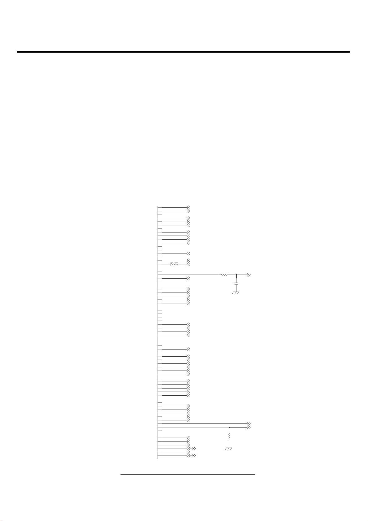
A. RTR6235(WCDMA_Tx, GSM_Tx/Rx)
ESM6270 controls RF part(RTR6235) using these signals.
• SBST : SSBI I/F signals for control Sub-chipset
• PA_ON1 : Power AMP on RF part
• RX0_I/Q_M/P, TX_I/Q_M/P : I/Q for T/Rx of RF
• TX_AGC_ADJ : control the gain of the Tx signal prior to the power amplifier
• DAC_REF : Reference input to the ESM Tx data DACs
Figure. Schematic of RF Interface of ESM6270
PA_ON1_GPIO2
CAMCLK_PO_GP_MN_GPIO13
XMEM1_CS_N3_SDRAM1_CS_N1_GPIO77
UART2_DP_RX_DATA_GPIO89
AUX_PCM_CLK_GRFC14_GPIO80
AUX_PCM_DIN_GRFC13_GPIO14
AUX_PCM_DOUT_GRFC12_GPIO103
AUX_PCM_SYNC_GRFC11_GPIO102
GRFC9_GPIO12
USB_RX_DATA_GPIO29
XMEM2_CS_N2_GPIO35
XMEM2_CS_N3_GPIO36
XMEM1_CS_N1_GPIO76
UART3_RFR_N_GPIO87
SYNTH0_GP_PDM0_GPIO92
GP_PDM2_PA_RAN_GE1
GP_PDM1_PA_RAN_GE0
GRFC5_AUX_SBST_GPIO8
GRFC4_AUX_SBCK_GPIO7
GRFC1_AUX_SBDT_GPIO4
BT_TX_RX_N_GPIO21
GPIO28
LCD_EN_GPIO37
GPIO43
SYNTH2_GPIO65
GPIO66
SBST1_GPIO93
TX_AGC_ADJ
TRK_LO_ADJ
TCXO_EN_GPIO94
PA_ON0
Q_OUT_N
Q_OUT
I_OUT_N
I_OUT
DAC_REF
Q_IM_CH1
Q_IP_CH1
I_IM_CH1
I_IP_CH1
Q_IM_CH0
Q_IP_CH0
I_IM_CH0
I_IP_CH0
TRST_N
TCK
TMS
TDO
RTCK
TX_ON_GRFC10
GRFC8_GPIO11
GRFC7_GPIO10
GRFX6_GPIO9
GRFC3_GPIO6
GRFC2_GPIO5
GRFC0_GPIO3
BT_CLK_GPIO25
BT_SBST_GPIO24
BT_SBCK_GPIO23
BT_SBDT_GPIO22
BT_DATA_GPIO20
D5
J21
A6
N19
W15
AA15
AE13
H9
B6
F8
AA1
Y6
L25
H6
F18
H18
R215 0
H13
L13
F19
F17
A12
B12
A13
B13
F12
W23
V23
V25
W25
AA25
Y25
AB25
AC25
D17
H17
H15
D16
F15
D15
TDI
A17
H16
K19
N21
G4
J8
H12
B4
T23
T19
D11
H10
F10
D9
A8
B8
G23
F23
E26
E25
H21
R19
LIN_INVERTER
LIN_MOTOR_EN
LCD_IF_MODE
USB_SELECT_N
CAM_MODE3_N
LCD_LDO_EN
MICROSD_DETECT
HOOK_SENSE_N
RMT_INT
HP_AMP_EN
LCD_RESET_N
MMP_INT_N
TCXO_EN
TX_QM
TX_QP
TX_IM
TX_IP
DAC_REF
RX_QM
RX_QP
RX_IM
RX_IP
LIN_PWM_MAG
JTAG_TRST_N
JTAG_TCK
JTAG_TMS
JTAG_TDI
JTAG_TDO
JTAG_RTCK
MMP_HPCM_CLK
MMP_HPCM_DI
MMP_HPCM_DO
MMP_HPCM_FSYNC
TX_ON
ANT_SEL1
ANT_SEL0
CAM_MODE1_N
FM_INTX
FM_BUSEN
BT_CLK
BT_SBST
BT_SBCK
BT_SBDT
BT_TX_RX_N
BT_DATA
2KR211
R213
NA
C223
33nF
TRK_LO_ADJ
GSM_PA_BAND
GSM_PA_EN
Page 45

LGE Internal Use Only
Copyright © 2008 LG Electronics. Inc. All right reserved.
Only for training and service purposes
B. the others
• TRK_LO_ADJ : TCXO(19.2M) Control
• PA_ON : WCDMA(2100) TX Power Amp Enable
• ANT_SEL[0-2] : Ant Switch Module Mode Selection(WCDMA,GSM Tx/Rx,DCS-PCS Tx/Rx)
• GSM_PA_BAND : GSM/DCS-PCS Band Selection of Power Amp
• GSM_PA_RAMP : Power Amp Gain Control of APC_IC
• GSM_PA_EN : Power Amp Gain Control Enable of APC_IC
3. TECHNICAL BRIEF
- 46 -
Page 46
3.9.2 MSM Sub System
3.9.2.1 SIM Interface
SIM interface scheme is shown in Figure.
And, there control signals are followed
• SIM_CLK : SIM Clock
• SIM_Reset : SIM Reset
• SIM_Data : SIM Data T/Rx
3.9.2.2 UART Interface
UART signals are connected to ESM GPIO through IO connector with 115200 bps speed.
LGE Internal Use Only
Copyright © 2008 LG Electronics. Inc. All right reserved.
Only for training and service purposes
3. TECHNICAL BRIEF
- 47 -
GPIO_Map Name Note
GPIO_96 UART_RXD Data_Rx
GPIO_95 UART_TXD Data_Tx
Table. UART Interface
Figure. SIM Interface
SIM CLK
SIM Reset
ESM6270
SIM Data
PM6635
VREG_UIM 2.85V
SIM CLK
SIM Reset
SIM Data
SIM
Page 47
LGE Internal Use Only
Copyright © 2008 LG Electronics. Inc. All right reserved.
Only for training and service purposes
3.9.2.3 USB
The ESM6270 device contains a Universal Serial Bus (USB) interface to provide an efficient
interconnect between the mobile phone and a personal computer (PC). The USB interface of the
ESM6270 was designed to comply with the definition of a peripheral as specified in USB Specification,
Revision 1.1. Therefore, by definition, the USB interface is also compliant as a peripheral with the USB
Specification, Revision 2.0.
The USB Specification Revision 1.1 defines two speeds of operation, namely low-speed (1.5 Mbps)
and full-speed (12 Mbps), both of which are supported by the ESM6270.
3. TECHNICAL BRIEF
- 48 -
Figure. Schematic of USB block(ESM6270 Side & PM6635 Side)
Table. USB Signal Interface
Name Note
USB_DAT Data to/from ESM
USB_SE0 Data to/from ESM
USB_OE_N Out-Put Enable of Transceiver
USB_VBUS USB_Power From Host(PC)
USB_D+ USB Data+ to Host
USB_D- USB Data- to Host
C528
4.7u
USB_DAT_VP
USB_OE_TP_N
USB_SE0_VM
MMC_CMD_GPIO30
GPIO40
D7
D6
GPIO42
N26
N23
N25
MMC_DATA_SDCC_DAT0_GPIO32
L14
H14
M16
USB_VBUS
47KR514
C540 4.7u
USB_OE_N
USB_CNT_N
USB_DAT
MSM_USB_D+
USB_SE0
MSM_USB_D-
12
VREG_5V
13
USB_OE_N
14
VSW_5V
15
USB_CTL_N
16
USB_VBUS
17
USB_DAT
18
USB_D_P
19
USB_SE0
20
USB_D_M
21
GP1_DRV_N(MPP7)
PS_HOLD
PM_INT_N
USB_SE0
USB_DAT
USB_OE_N
MSM_MICROSD_CMD
MSM_MICROSD_DATA[0]
Page 48

3.9.3 HKADC(House Keeping ADC)
The ESM6270 device has an on-chip 8-bit analog-to-digital converter (HKADC) which is tended to
digitize DC signals corresponding to analog parameters such as battery voltage, temperature, and RF
power levels. The ESM6270 device has six analog input pins which are multiplexed to the input of the
internal HKADC.
LGE Internal Use Only
Copyright © 2008 LG Electronics. Inc. All right reserved.
Only for training and service purposes
3. TECHNICAL BRIEF
- 49 -
Figure. ESM6270HKADC Block diagram
Table. HKADC channel table
Channel Signal Note
HKADC0 AMUX_OUT RF PAM Temperature Check
HKADC1 VBATT_SENSE Battery voltage level
HKADC2 REF_ADC ADC Reference voltage
HKADC3 TTY_ADC_DET Ear jack Detection for TTY
HKADC4 PCB_Rev_ADC PCB Version Check
HKADC5 Battery_THERM Battery Temperature Check
Page 49

LGE Internal Use Only
Copyright © 2008 LG Electronics. Inc. All right reserved.
Only for training and service purposes
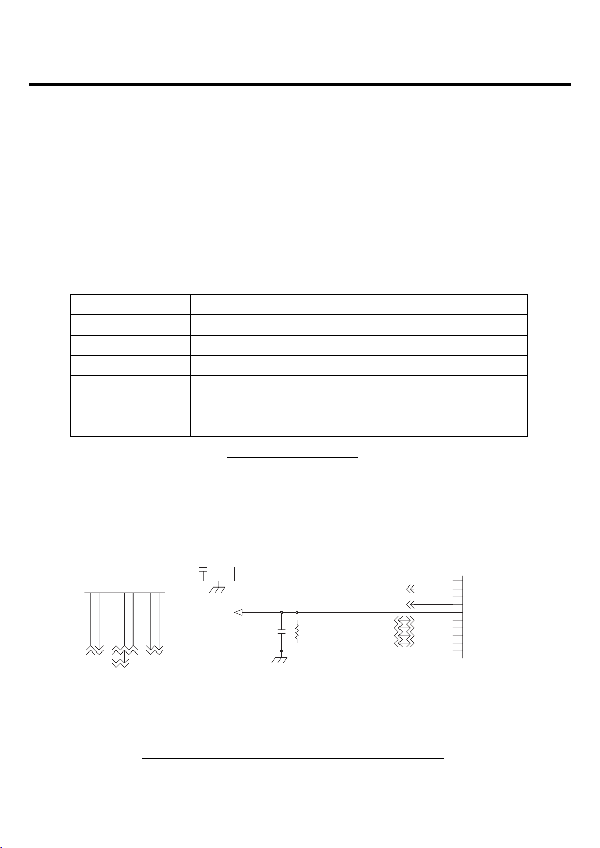
3.9.4 Key Pad
There are 5 key buttons. Shows the Key Matrix & Keypad circuit. ‘END’ Key is connected to
PMIC(PM6635).
3. TECHNICAL BRIEF
- 50 -
Table. Key Matrix Mapping Table
COL(0) COL(1)
ROW(0) Lock Capture
ROW(1) AF
ROW(2) SEND CLR
Figure. Main Keypad Circuit
VREG_MSMP_2.7V
KEY_ROW[2]
KEY_COL[0]
KEY_COL[1]
R701
EVLC14S02050VA701
51K
EVLC14S02050VA702
VA703 EVLC14S02050
701700
CLRSEND
Page 50

LGE Internal Use Only
Copyright © 2008 LG Electronics. Inc. All right reserved.
Only for training and service purposes
3. TECHNICAL BRIEF
- 51 -
Figure. END Keypad Circuit
Figure. Side Keypad Circuit
900
SW900
KEY_ROW[0]
KEY_ROW[1]
KEY_COL[0]
KEY_COL[1]
PM_ON_SW_N
LOCK KEY
END
END
CAMERA
FOCUS
VA700
EVL14K02200
ON_SW KEY
Page 51

- 52 -
3. TECHNICAL BRIEF
LGE Internal Use Only
Copyright © 2008 LG Electronics. Inc. All right reserved.
Only for training and service purposes
3.9.5 Camera Interface
U990 Installed a 5M Pixel and 0.3Mega Camera.
Below figure shows the camera board to board connector and camera I/F signal.
Figure. Camera PCB Board to Board Connector
5M CAMERA INTERFACE
R607
33
10R601
10R602
VA600ICVL0518100Y500FR
C610
10p
C611
10p
C612
10p
MMP_I2C_SCL
MMP_I2C_SDA
MMP_CAM_MCLK
MMP_CAM_VSYNC
MMP_CAM_HSYNC
MMP_CAM_RESET_N MMP_CAM_INT
STROBE_TRIGGER
5M_CAM_DATA[6] 5M_CAM_DATA[7]
5M_CAM_DATA[4] 5M_CAM_DATA[5]
5M_CAM_DATA[2] 5M_CAM_DATA[3]
5M_CAM_DATA[0] 5M_CAM_DATA[1]
CAM_VDD_CORE_1.2V
R603 10
10R604
VA602
C613
10p
C605
0.1u
GB042-30S-H10-E3000
30
29
28
27
26
25
24
23
22
21
20
19
18
17
16
C614
0.1u
EVLC18S02015
CAM_VDD_AF_2.7V
C601
C602
0.1u
1u
CN600
1
2
3
4
5
6
7
8
9
10
11
12
13
14
15
CAM_VDD_SA_2.7V
CAM_VDD_IO_2.7V
C600
10u
0.1uC609
CAM_VDD_SD_1.8V
1uC608
C606
0.1u
C607
0.1u
10R608
MMP_CAM_PCLK
ICVL0518100Y500FR VA601
Page 52

The MEGA Camera module is connected to Main PCB with 30pin Board to Board connector Its
interface is dedicated camera interface port in Multimedia chip. The camera port supply 13MHz master
clock to camera module, vertical sync signal, horizontal sync signal, reset signal and 8bits data from
camera module. The camera module is controlled by I2C port from Multimedia chip.
- 53 -
3. TECHNICAL BRIEF
LGE Internal Use Only
Copyright © 2008 LG Electronics. Inc. All right reserved.
Only for training and service purposes
Table. Interface between MEGA Camera Module and MAIN PCB (in camera module)
[ Pin Description ]
1 AF_GND - - - - Ground(Auto Focus)
2 GND - - - - Ground
3 VDD_AF(2.8V) - - - - Voltage Supply(Auto Focus)
4 SCL I/O HiZ Active HiZ I2C Serial Bus Clock
5 GND - - - - Ground
6 SDA I/O HiZ Active HiZ I2C Serial Bus Data I/O
7 VDD_SA(2.8V) - - - - Voltage Supply(Sensor Analog)
8 VSYNC O Low HiZ HiZ Vertical Synchronization Signal
9 VDD_IO(2.8or1.8V) - - - - Voltage Supply(I/O)
10 HSYNC O Low HiZ HiZ Horizontal Synchronization Signal
11 TRIG O Low Low Low Interrupt Line Signal
12 XRST I - - - System Reset
13 GND - - - - Ground
14 STRB O Low Low Low LED/Xenon Strobe Contol
15 D[7] O Low HiZ HiZ Digital Video Data(MSB)
16 D[6] O Low HiZ HiZ Digital Video Data
17 D[5] O Low HiZ HiZ Digital Video Data
18 D[4] O Low HiZ HiZ Digital Video Data
19 D[3] O Low HiZ HiZ Digital Video Data
20 D[2] O Low HiZ HiZ Digital Video Data
21 D[1] O Low HiZ HiZ Digital Video Data
22 D[0] O Low HiZ HiZ Digital Video Data(LSB)
23 VDD_SD(1.8V) - - - - Voltage Supply(Sensor Digital)
24 GND - - - - Ground
25 DCK O Low HiZ HiZ Digital Video Data Clock
26 MCK I - - - System Clock Input
27 GND - - - - Ground
28 VDD_L(1.2V) - - - - Voltage Supply(DSP Core)
No
Symbol
I/O
Description
State at
reset
State at
power save
State at
power off
Page 53

LGE Internal Use Only
Copyright © 2008 LG Electronics. Inc. All right reserved.
Only for training and service purposes
3.9.6 LCD Module (LS030B3UX01 : SHARP)
- The IM220DBN2A model is a Color TFT Main supplied by SHARP.
This LCD Module has a 3.0 inch diagonally measured active display area with 240(RGB)X400
resolution. each pixel is divided into Red, Green and Blue sub-pixels and dots which are arranged in
vertical stripes.
* Features
- Display mode(Main LCD) : Normally Black, Transmissive VA mode 265K colors
- LCD Driver IC : LS030B3UX01(Magnachip)
- Driving Method : A-Si TFT Active Matrix
- 16 bit CPU interface Parallel
3. TECHNICAL BRIEF
- 54 -
Figure. LCD Module Block Diagram
ESM6270
LCD_RESET_N
MMP_CS_N
EBI2_OE_N
EBI2_WE_N
EBI2_ADDR[11]
Multimedi a
Chip
EBI2_DAT A[0:15]
LCD_MAKER_ID
LCD_IF_MOD
E
MMP_LCD_CS_N
MMP_LCD_RD_N
MMP_LCD_WE_N
MMP_LCD_ADS
MMP_LCD_DATA[0:15 ]
LCD 3.0î
TFT(WQVGA)
Page 54

LGE Internal Use Only
Copyright © 2008 LG Electronics. Inc. All right reserved.
Only for training and service purposes
3. TECHNICAL BRIEF
- 55 -
3.9.7 Display
LCD module is connected to Main PCB with 40 pin B TO B connector.
The LCD module is controlled by 16-bit EBI2 in ESM6270 via Multimedia Chip.
1.0T, Socket
OTP Program Pin
ENBY0036001
GB042-40S-H10-E3000
C324 22p
C321
0.1u
LCD_VDD_2.8V
R316 51
0R318
R314 51
C326
22p
39
22
40
23
24
25
26
27
28
29
ICVN0505X150FR
VA300
5
6
7
8
9
21
30
31
32
33
34
35
36
37
38
1
10
11
12
13
14
15
16
17
18
19
2
20
3
4
VA301
CN300
51R315
22pC325
C320
NA
22pC322
C323 22p
R317 51
LCD_VSYNC_OUT
LCD_MAKER_ID
MMP_LCD_WE_N
MMP_LCD_VSYNC_OUT
WLED_PWR
WLED_2
WLED_4
WLED_5
MMP_LCD_VSYNC_IN
LCD_IF_MODE
LCD_DATA[0]
LCD_DATA[1]
LCD_DATA[2]
LCD_DATA[3]
LCD_DATA[4]
LCD_DATA[5]
LCD_DATA[6]
LCD_DATA[7]
LCD_DATA[14]
LCD_DATA[15]
LCD_DATA[8]
LCD_DATA[9]
LCD_DATA[10]
LCD_DATA[11]
LCD_DATA[12]
LCD_DATA[13]
WLED_1
WLED_3
MMP_LCD_ADS
MMP_LCD_CS_N
LCD_RESET_N
MMP_LCD_RD_N
FL303 ICVE10184E150R500FR
G15G2
10
INOUT_A1
1
2
INOUT_A2
INOUT_A3
3
4
INOUT_A4
9
INOUT_B1
INOUT_B2
8
7
INOUT_B3
INOUT_B4
6
5
G110G2
1
INOUT_A1
INOUT_A2
2
3
INOUT_A3
INOUT_A4
4
INOUT_B1
9
8
INOUT_B2
INOUT_B3
7
6
INOUT_B4
ICVE10184E150R500FRFL302
INOUT_A3
3
4
INOUT_A4
9
INOUT_B1
INOUT_B2
8
7
INOUT_B3
INOUT_B4
6
FL300 ICVE10184E150R500FR
G15G2
10
INOUT_A1
1
2
INOUT_A2
2
3
INOUT_A3
INOUT_A4
4
INOUT_B1
9
8
INOUT_B2
INOUT_B3
7
6
INOUT_B4
ICVE10184E150R500FRFL301
5
G110G2
1
INOUT_A1
INOUT_A2
MMP_LCD_DATA[9]
MMP_LCD_DATA[10]
MMP_LCD_DATA[11]
MMP_LCD_DATA[12]
MMP_LCD_DATA[13]
MMP_LCD_DATA[14]
MMP_LCD_DATA[15]
LCD_DATA[12]
LCD_DATA[13]
LCD_DATA[14]
LCD_DATA[15]
MMP_LCD_DATA[0]
MMP_LCD_DATA[1]
MMP_LCD_DATA[2]
MMP_LCD_DATA[3]
MMP_LCD_DATA[4]
MMP_LCD_DATA[5]
MMP_LCD_DATA[6]
MMP_LCD_DATA[7]
MMP_LCD_DATA[8]
LCD_DATA[0]
LCD_DATA[1]
LCD_DATA[2]
LCD_DATA[3]
LCD_DATA[4]
LCD_DATA[5]
LCD_DATA[6]
LCD_DATA[7]
LCD_DATA[8]
LCD_DATA[9]
LCD_DATA[10]
LCD_DATA[11]
Page 55

LGE Internal Use Only
Copyright © 2008 LG Electronics. Inc. All right reserved.
Only for training and service purposes
3.9.7.1 Audio Signal Processing & Interface
Audio signal processing is divided uplink path and downlink path.
The uplink path amplifies the audio signal from MIC and converts this analog signal to digital signal
and then transmits it to DBB Chip (ESM6270).
This transmitted signal is reformed to fit in GSM & WCDMA frame format and delivered to RF Chipset.
The downlink path amplifies the signal from DBB chip (ESM6270) and outputs it to receiver (or
speaker).
The receive path can be directed to either one of two earphone amplifiers or the auxiliary output.
The outputs earphone1 (EAR1OP, EAR1ON) and auxiliary out (LINE_OP, LINE_ON) are differential
outputs. Earphone2 (HPH_L, HPH_R) is a single-ended output stage designed to drive a headset
speaker.
The microphone interface consists of two differential microphone inputs, one differential auxiliary input
and a two-stage audio amplifier.
3. TECHNICAL BRIEF
- 56 -
Figure. Audio Interface Detailed Diagram(ESM6270)
Page 56
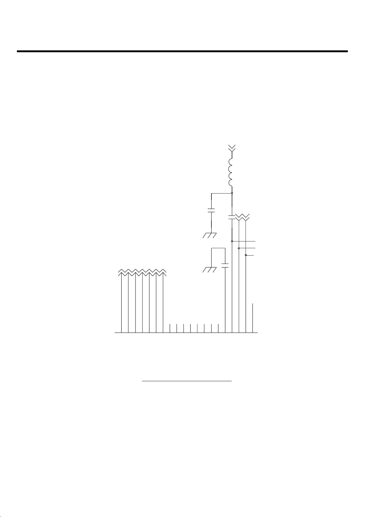
LGE Internal Use Only
Copyright © 2008 LG Electronics. Inc. All right reserved.
Only for training and service purposes
3. TECHNICAL BRIEF
- 57 -
ESM6270 Audio CODEC pins
Figure . Audio part schematics
MIC2P
L200
100nH
HP_R
HP_L
AC18
AC17
AA17
LINE_OP
LINE_ON
C200
10p
RCV+
RCV-
AF18
AE18
EAR1OP
EAR1ON
MICBIAS
T15
AA18
MICBIAS
AUXOUT
AC21
AC22
AA19
LINE_L_IP
LINE_L_IN
HPH_VREF
AC20
AC19
AF19
LINE_R_IP
LINE_R_IN
AE19
AUXIN
SPK_L
SPK_R
W17
HPH_L
HPH_R
0.1uC235
C236 0.1u
AF21
AF22
AUXIP
MIC2N
MIC1N
AF20
AE20
MIC2P
MIC1N
MIC1P
AA20
MIC1P
CCOMP
Page 57

- 58 -
3. TECHNICAL BRIEF
LGE Internal Use Only
Copyright © 2008 LG Electronics. Inc. All right reserved.
Only for training and service purposes
Figure . Audio part schematics
MICBIAS
C564
47p
EAR_MIC_P
SPM0204HE5-PB-3
G2
G1
O
MIC500
MIC
C563
P
4
3
2
1
R904
10u
C575
33p
C576
10p
22nC567
22nC568
C569
NA
MIC1N
MIC1P
NCS2200SQ2T2G
U902
2
GND
3
OUT
VCC
4
1
5
HOOK_SENSE_N
R905
10K
100K
VIN+
VIN-
VREG_MSMP_2.7V
5.1K
R907
R906 1M
C905
0.1u
Headset Hook Switch
Page 58

- 59 -
3. TECHNICAL BRIEF
LGE Internal Use Only
Copyright © 2008 LG Electronics. Inc. All right reserved.
Only for training and service purposes
Figure . Audio part schematics
AUDIO DAC/ADC, AMP etc. (WM8983)
SPK_R
FM_AUDIO_R
FM_AUDIO_L
SPK_L
C532 1u
HP_L
HP_R
VREG_5V
C514
C513
10u
0.1u
MIDI_3.3V
C518
C519
4.7u
0.1u
MMP_A_LRCLK
C530
12n
C533
R510
1K
4.7n
1uC535
1uC536
R516
1K
C542
4.7n
C547
12n
1uC548
1uC549
1uC541
MMP_ADI_ADCDAT
MMP_ADO_DACDAT
R511
18K
R517
18K
MMP_A_BCLK
MMP_A_MCLK
MID_MICP
CODEC_I2C_SCL
CODEC_I2C_SDA
C534
C539
1u
1u
R533
C516 C517
4.7u 0.1u
C520
4.7u
13 12
DCVDD
14
DBVDD
26
AVDD2
31
AVDD1
7
LRC
8
BCLK
9
ADCDAT
10
DACDAT
11
MCLK
4
RIP
5
RIN
6
R2_GPIO3
3
L2_GPIO2
1
LIP
2
LIN
19
AUXL
20
AUXR
15
CSB_GPIO1
16
SCLK
17
SDIN
0
C521
0.1u
VREG_WM_2.7V
VREG_MSME_1.8V
WM8983U502
DGND
AGND1
AGND2
VMID
MICBIAS
ROUT1
LOUT1
ROUT2
LOUT2
OUT3
OUT4
MODE
PGND
28
24
27
32
29
30
23
25
22
21
18
33
FB500
FB501
MIC2P
R519
C524
0.1u
100K
C525
10u
HP_EAR_R
HP_EAR_L
C543
NA
C544
NA
C531
NA
SPK_OUT+
SPK_OUT-
MIC_PWR
21
19
CN500
1
2
3
4
5
FB504
C550
NA
C551
NA
L504
2.2uH
VREG_MSMP_2.7V
R528 100K
FM_ANT
EAR_MIC_P
TV_OUT
MIDI_EAR_L
MIDI_EAR_R
Page 59

- 60 -
3. TECHNICAL BRIEF
3.9.7.2. Audio Mode
There are three audio modes (Voice call, speaker phone, MIDI/MP3).
Audio & Sound Main Component
There are 8 main components in KE990.
LGE Internal Use Only
Copyright © 2008 LG Electronics. Inc. All right reserved.
Only for training and service purposes
Headset MP3Headset
Headset MIDI BellHeadset
Speaker MP3Loud Mode
MP3
Speaker MIDI BellLoud Mode
MIDI
Speaker PhoneLoud Mode
Headset Voice CallHeadset
Speaker PhoneLoud ModeSpeaker phone
Receiver Voice Call
Description
Receiver Mode
Voice Call
DeviceMODE
Table. Audio Mode
-42 dB microphoneSPOB-413S42-
RC3310BC
CAM MIC7
32 ohm receiverEMR0906SPReceiver5
8 ohm SpeakerEMS1634APB1Speaker4
-42 dB microphoneSPM0204HE5-PBMain MIC6
Ear MICHC-MQD-LG059Ear MIC8
Analog Switch for MIC BIASNC7SB3157L6XAnalog Switch3
ADC/DAC, AB class SPK AMP
Base-Band Modem
Note
WM8983
ESM6270
Maker Part No.
Audio Codec
ESM6270
Component
2
1
Table. Audio main component list
Page 60

- 61 -
3. TECHNICAL BRIEF
3.10 Feature List
3.10.1 IC Characteristics
• MCP with Internal SDRAM, no need for external memory.
• Package: 180-pin TFBGA (8 x 8 mm)
• 90nm process
• Core voltage - 1.0 V
• IO voltage - Eleven strips, separate voltage between 1.8 and 3.3 V
3.10.2 Multimedia Performance
• Digital Still Camera support with ISP on chip up to 5M pixel.
- Photo-album and photo-editing capabilities.
- Superior quality, (e.g. including lens shading).
- Camera controls for flash, optical zoom,focus, shutter and iris.
• Camcorder operation as a DivX recorder /player at 30 fps CIF, VGA resolution. AVI file format with
MP3 audio.
• Player for general DivX content, up to 30 fps CIF resolution. MP3 or WMA audio.
• 3GPP MMS compliant video clip recorder, supporting CIF/QCIF H.263, MPEG4 recording with AMR
voice or AAC audio.
• Player for 3GPP MMS / streaming video clips, up to 30 fps CIF H.263, MPEG4, and H.264 with AMR
voice or AAC/Enhanced AACPlus audio.
• 3GPP-compliant videophone, with H.263 or MPEG4 video\ at QCIF 15 fps (full-duplex).
• MIDI player (for ring tones, melodies).
Compliant with 3GPP standards, including support for Mobile XMF for melodies with custom
instruments.
• Audio stereo recorder player MP3/WMA
• ID3 tags display
• Spectral bars
• Lyrics display
• Equalizer
• 3D Surround Audio
LGE Internal Use Only
Copyright © 2008 LG Electronics. Inc. All right reserved.
Only for training and service purposes
Page 61

- 62 -
3. TECHNICAL BRIEF
LGE Internal Use Only
Copyright © 2008 LG Electronics. Inc. All right reserved.
Only for training and service purposes
3.10.3 DRM
• MDTV Conditional access compliant to JSR-177 (AES and TDES)
• Key exchange support
• True RNG (Random Number Generator)
3.10.4 3D Graphics
• 3D hardware + software accelerator targeting VGA 30 fps games with PlayStation™-1 enhanced
quality.
- Setup and viewport transforms
- Bilinear and Trilinear texturing
- Multi-texturing
- Flat and Gourard shading
- 24-bit ARGB support
- Compressed textures (2 bits/texel)
- Mipmaping
- Full scene anti-aliasing (x4 / x16)
- 16-bit Z-buffer
- 4-bit stencil buffer
- Fog
- Alpha blending
- Dot3 bump mapping
• Fill rate: 120M pixels/sec
• Polygon rate 0.8M triangles/sec
3.10.5 Image Sensor
• 10/12/14/16-bit RGB - Bayer Grid
- CMOS up to 5MP
- CCD up to 5MP
- Pixel clock - Up to 90 MHz.
- Active pixel rate - up to 75M pixels/sec:
- 15fps @ 5MP
- 25fps @ 3MP
- 30fps @ 2MP
- Black-level evaluation and correction
- Defective pixel correction
- Auto exposure and White-balance
- Edge enhancement and auto focus.
Page 62

LGE Internal Use Only
Copyright © 2008 LG Electronics. Inc. All right reserved.
Only for training and service purposes
3. TECHNICAL BRIEF
- 63 -
- Lens shading correction
- Polyphase image scaling.
- Digital zoom up to X4 in 16 steps
- 8/16-bit YCbCr - 4:2:2
- Input streaming bus - as CCIR601
- Progressive (CMOS/CCD sensors) or interlaced (PAL/NTSC decoders) mode
- Pixel clock - Up to 120 MHz (8-bit), 60Mhz (16-bit)
- Input resolution - Up to 5M pixels
- Auto focus
- Polyphase image scaling
- Digital zoom up to X4 in 16 steps
3.10.6 LCD Port
• Output resolution - up to VGA
• Supports dual-panels (two LCDs)
• Bypass from Host port to LCD CPU bus
• Up to 18-bit color depth (262K colors)
• CPU bus 8/9/16/18 bit compliant to all known vendors.
• RGB bus 3/6/18 bit up to 30Mhz clock
3.10.7 TV-out Port
• Composite analog interface
- NTSC-M
- PAL-B,D,G,H,I
3.10.8 Video and Graphics Postprocessing
• Handles Video (YUV) and Graphic (RGB)
• Video de-blocking
• Blending of video and graphics - up to 256 levels of blending
• Resizing (upscale and downscale) using quality polyphase filter
• Rotation and flip - 90, 180 and 270 degrees
• Picture brightness, contrast, and saturation control
• Display gamma adjustment
• Color space reduction
Page 63

- 64 -
3. TECHNICAL BRIEF
3.10.9 Serial Audio Ports
• ZR3453X has two audio/voice ports: one port is used for host bypass connection, and another for
connecting to a codec or to a Bluetooth voice port.
- PCM master/slave
- I2S master/slave (5 lines including clock)
- AC’ 97 master (5 lines including AC-Link reset)
- Audio output master clock (I2S), up to 48 MHz
- Supports sample rates of 8, 11.025, 16, 22.05, 24, 32, 44.1 or 48 kHz
3.10.10 Serial Data Ports
• I2C Multiple device support 100 and 400 kHz
• UART with flow control up to 3Mb/sec
• SPI port with Bit clock up to 40 MHz
- (Motorola, National microwire, TI synchronous serial interface )
3.10.11 Mass Storage
• High-speed SD/MMC I/F
• NAND-flash storage
• SPI-flash
• CE - ATA HDD.
• SDIO peripherals
3.10.12 USB
• USB 2.0 High speed/full speed
• USB On The Go
• USB applications:
- USB mass storage
- PictBridge
- Webcam
LGE Internal Use Only
Copyright © 2008 LG Electronics. Inc. All right reserved.
Only for training and service purposes
Page 64

- 65 -
3. TECHNICAL BRIEF
3.10.13 Host Port
• Two flavors:
- Generic interface 8/16-bit Intel style.
Connects as memory map (4-bit address)
- LCD like 8/9/16 bit multiplexed bus.
Connects as an LCD (1-bit address)
• Bypass mode - From Host port up to two LCDs, audio codec and other peripherals
• Support for messaging and data transfers (DMA)
3.10.14 Clocks
• Main clock input frequency, 10 to 31 MHz:
- Directly from system PMU main clock and bypass its control
- Embedded crystal oscillator (12Mhz)
- Optional GPS TCXO
• Four configurable clock-out pins to drive external components:
e.g. Audio codec, Sensor, PWM)
3.10.15 Boot
• Host boot
• Standalone boot
3.10.16 Debug
• JTAG for code debug
• UART for fast system ramp up
3.10.17 Power
• Very low power consumption, smaller than150mW for all intense multimedia applications.
• Low power sleep mode 100 µW
- Host can control display audio and peripherals via bypass
Light sleep mode 500 µW
- Specifically for GPS accurate off-line tracking
LGE Internal Use Only
Copyright © 2008 LG Electronics. Inc. All right reserved.
Only for training and service purposes
Page 65

- 66 -
3. TECHNICAL BRIEF
Figure 3.10 presents a typical multimedia cellular phone system where ZR3453X is used as a cocoprocessor. In this system, ZR3453X is connected to the following devices:
• Baseband chip (the host)
• CCD/CMOS Image Sensor for capturing video and still
• LCD panel(s)for displaying video
• Audio CODEC (A2D, D2A) for capturing voice and playing voice/music
• Media Flash (SmartMedia, NANDFlash, MMC or SD) to store media data (two active I/F, e.g. one
NAND and one SD)
• Connector to TV
LGE Internal Use Only
Copyright © 2008 LG Electronics. Inc. All right reserved.
Only for training and service purposes
[ Figure 3.10 ]
Page 66

- 67 -
3. TECHNICAL BRIEF
3.11 Multimedia Chip Interface
3.11.1 Host Interface
3.11.1.1 Host Interface
The HOST interface connects the ZR3453X and the host processor (a handset baseband chip) in two
optional modes:
• On the host memory bus.
• On the host LCD bus.
LGE Internal Use Only
Copyright © 2008 LG Electronics. Inc. All right reserved.
Only for training and service purposes
[ Block Diagram ]
[ Schematics ]
VREG_MSMP_2.7V
0R311
B8
A8
B7
B9
A7
A10
A9
C8
C7
D12
C10
C12
C13
C14
B14
C11
B13
A14
A13
B12
A12
B11
A11
C9
B10
L13
M13
L12
HCS0N
HCS1N
HRDN
HWRN
HGINTN
HA11
HA12
HA13
HA14
HD0
HD1
HD2
HD3
HD4
HD5
HD6
HD7
HD8
HD9
HD10
HD11
HD12
HD13
HD14
HD15
NCSN
NALE
NCLE
MMP_INT_N
R310
10K
EBI2_ADDR[11]
EBI2_ADDR[12]
EBI2_ADDR[13]
EBI2_ADDR[14]
EBI2_DATA[0:15]
MMP_CS_N
NAND_ALE
EBI2_OE_N
EBI2_WE_N
EBI2_DATA[0]
EBI2_DATA[1]
EBI2_DATA[2]
EBI2_DATA[3]
EBI2_DATA[4]
EBI2_DATA[5]
EBI2_DATA[6]
EBI2_DATA[7]
EBI2_DATA[8]
EBI2_DATA[9]
EBI2_DATA[10]
EBI2_DATA[11]
EBI2_DATA[12]
EBI2_DATA[13]
EBI2_DATA[14]
EBI2_DATA[15]
R313 NA
Page 67
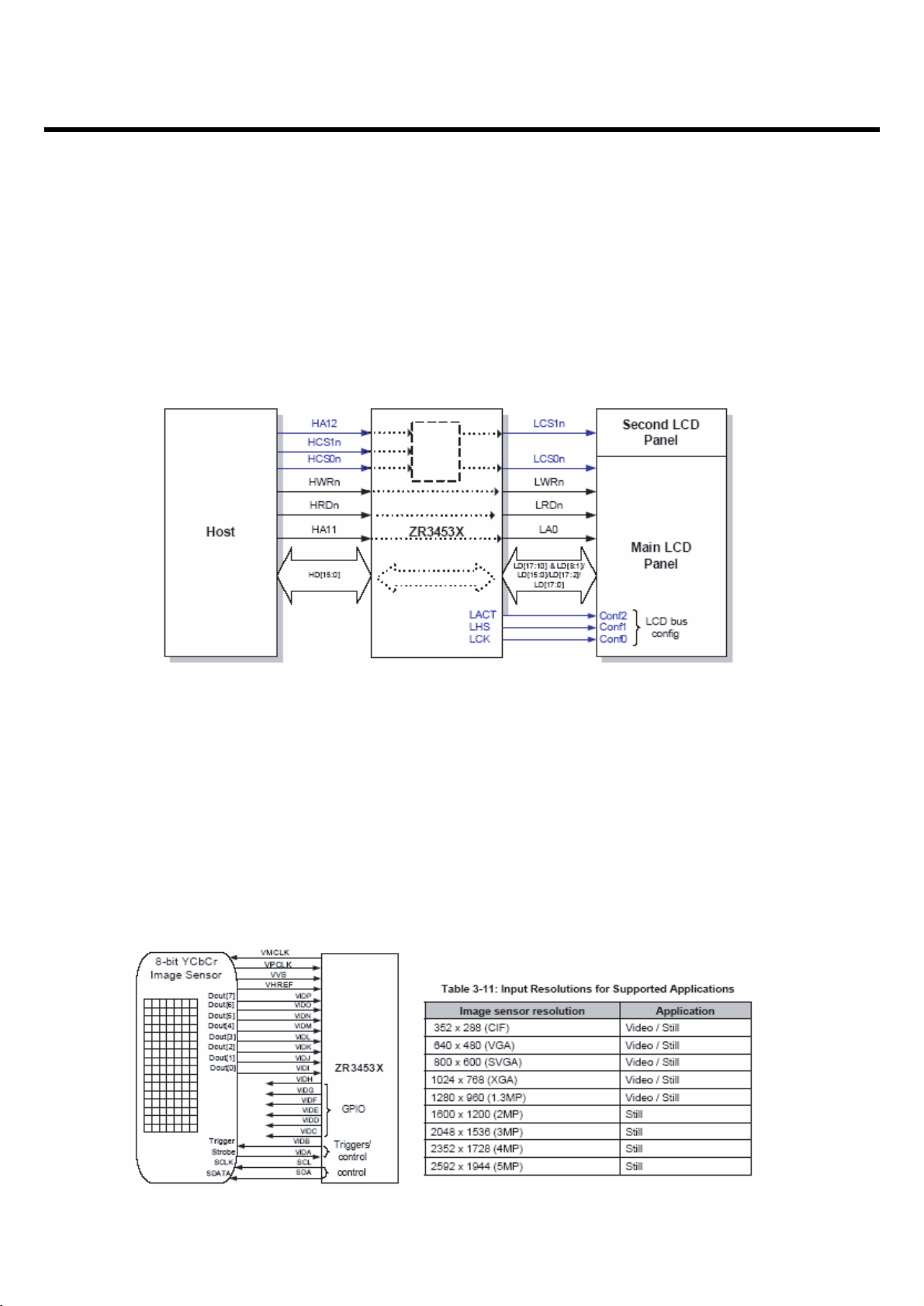
- 68 -
3. TECHNICAL BRIEF
3.11.2 Host - LCD - Bypass mode
The Host-LCD Bypass bypasses the host interface pins to the LCD pins.
This means that the bus transactions performed by the host are transferred to the LCD pins, enabling
the host to have full control over one or two LCD panels, even when the ZR3453X is in sleep mode.
This is the default mode.
3.11.3 Camera interface
ZR3453X connects with the CCD or CMOS Image Sensor (CIS) via its image sensor port.
ZR3453X supports several system configurations:
• CCD bayer 10,12,14,16 bit (ZR34532 only)
• CMOS bayer 10,12,14,16 bit
• YCbCr 8 bit
• YCbCr 8 bit with pixel valid
• YCbCr 16 bit
LGE Internal Use Only
Copyright © 2008 LG Electronics. Inc. All right reserved.
Only for training and service purposes
Page 68

- 69 -
3. TECHNICAL BRIEF
3.11.4 LCD Interface
The ZR3453X LCD port supports mobile LCD panels of upto VGA size and upto 60fps refresh rate.
There are various bus formats and color depth up to 18-bit (262K colors).
3.11.5 TV out Interface
The display data is converted to video with video-encoder according to CCIR-601 and sampled by 10bit DAC and transmitted over an analog pad as a composite video signal.
This mode is used in a system where ZR3453X is connected gluelessly to a TV screen that requires
real-time display data.
ZR3453X generates TV signal according to the NTSC and PAL standards.
The TVDATA pin can drive a full video level signal directly into a 75 terminated TV cable.
LGE Internal Use Only
Copyright © 2008 LG Electronics. Inc. All right reserved.
Only for training and service purposes
[ Block Diagram ]
[ Schematics ]
[ Block Diagram ] [ Schematics ]
N12
VIDI
N7
VIDJ
L8
VIDK
P13
VIDL
L9
VIDM
N13
VIDN
M11
VIDO
M9
VIDP
B5
LD0
A5
LD1
B6
LD2
B4
LD3
A4
LD4
C3
LD5
A3
LD6
A2
LD7
A1
LD8
B2
LD9
B1
LD10
B3
LD11
C1
LD12
C2
LD13
C5
LD14
C6
LD15
D3
LD16
D1
LD17
A6
LCS0N
D2
LCS1N
D5
LRDN
C4
LWRN
D4
LA0
E1
LCK
E4
LHS
E3
LVS
E2
LACT
TP300
TP301
MMP_CAM_DATA[0]
MMP_CAM_DATA[1]
MMP_CAM_DATA[2]
MMP_CAM_DATA[3]
MMP_CAM_DATA[4]
MMP_CAM_DATA[5]
MMP_CAM_DATA[6]
MMP_CAM_DATA[7]
MMP_LCD_DATA[0]
MMP_LCD_DATA[1]
MMP_LCD_DATA[2]
MMP_LCD_DATA[3]
MMP_LCD_DATA[4]
MMP_LCD_DATA[5]
MMP_LCD_DATA[6]
MMP_LCD_DATA[7]
MMP_LCD_DATA[8]
MMP_LCD_DATA[9]
MMP_LCD_DATA[10]
MMP_LCD_DATA[11]
MMP_LCD_DATA[12]
MMP_LCD_DATA[13]
MMP_LCD_DATA[14]
MMP_LCD_DATA[15]
MMP_LCD_CS_N
MMP_LCD_RD_N
MMP_LCD_WE_N
MMP_LCD_ADS
MMP_LCD_VSYNC_IN
MMP_LCD_VSYNC_OUT
TV_OUT
C334
330p
C331
22p
L300
2.2uH
C335
330p
G14
TVDATA
F13
TVREF
75
390
R339
R338
392ohm 1%
Page 69

- 70 -
3. TECHNICAL BRIEF
3.11.6 Audio Interface
In this configuration ZR3453X is connected to an external audio codec.
There are three possible configurations:
• Audio/Voice codec with two ports: PCM and I2S
• Audio/Voice codec with one port: I2S
• Audio/voice/data codec with one port: AC97
In all configurations ZR3453X connects its external audio ports to the codec single or two
ports.
The host uses its internal voice codec for voice communication. There is no bypass of voice.
The host controls the codec configuration via I2C bus directly. The host codec analog audio output is
connected to the external audio codec and muxed with the codec audio path from the ZR3453X on the
way is to the speaker.
The microphone is connected to the external audio codec and the baseband internal codec.
ZR3453X appears in Figure 3.11 as a master on the bit clock and frame sync. This is only one of the
possible configurations.
In external audio configuration ZR3453X can run all the Audio/voice applications including
conversation recording .
LGE Internal Use Only
Copyright © 2008 LG Electronics. Inc. All right reserved.
Only for training and service purposes
[ Figure 3.11 ]
Page 70

- 71 -
3. TECHNICAL BRIEF
3.11.7 USB interface
ZR3453X is a USB 2.0 Device or On-the-Go dual-role device (OTG) with the following characteristics:
• Complies with USB (Universal Serial Bus) 2.0 specifications
• Complies with On-the-Go Supplement 1.0a
• Integrated 45-ohm termination, 1.5Kilohm pull-up and 15-Kilohm pull-down resistors.
• Supports 480-Mbps high-speed, 12-Mbps full-speed and 1.5Mbps low-speed (Host mode only) data
transmission rates.
• Control + 4 endpoints:
- EP0 - two-way Control
- 2-input , 2-output - Bulk, INT or ISO
• Suspend, resume, reset and SOF signaling
3.11.8 MMC interface
LGE Internal Use Only
Copyright © 2008 LG Electronics. Inc. All right reserved.
Only for training and service purposes
AGND_USBT
AGND_VDAC
L5
K5
F12
AGND_USBC
USB_SELECT_N
UDP
UDN
UVBUS
UID
URSET
P3
P4
J4
P6
M7
R340
3.4K
1%
3.3K
0R335
R345
100K
MMP_USB_D+
MMP_USB_D-
VREG_5V
C336
0.01u
MSM_USB_D-
MMP_USB_D-
+VPWR
U304FSUSB30UMX
10
SEL
9
VCC
8
_OE
7
HSD1-
6
HSD2-
HSD1+
HSD2+
D+
GND
1
2
3
4
5
D-
MSM_USB_D+
MMP_USB_D+
USB_D+
USB_D-
Page 71

- 72 -
3. TECHNICAL BRIEF
ZR3453X has a dedicated port for multimedia cards. It can support SD (Secure Digital) cards and
SecureMMC (standard multimedia cards with security functions).
The same port can be used for HDD CE_ATA connection or SDIO to peripheral devices (e.g.; MDTV
front-end).
MMC
• MMC v4
• Dual voltage (separate IO power domain, host GPIO control)
• 1 or 4 bit cards
• Multiple cards support (if dual-voltage or high-speed interface are not used)
• Up to 43 MHz bit clock
SD
• 1 or 4 bit bus support
• High-Speed SD, up to 43 MHz bit clock
3.11.9 Power Domain
LGE Internal Use Only
Copyright © 2008 LG Electronics. Inc. All right reserved.
Only for training and service purposes
SDAT0
SDAT1
SDAT2
SDAT3
SCMD
SCLK
SWP
VMCLK
VPCLK
VHREF
VVS
F1
F2
E5
F3
H2
G1
G3
P12
P10
M12
K12
MMP_MICROSD_DATA[0]
MMP_MICROSD_DATA[1]
MMP_MICROSD_DATA[2]
MMP_MICROSD_DATA[3]
33R312
MMP_MICROSD_CMD
MMP_MICROSD_CLK
MMP_CAM_MCLK
MMP_CAM_PCLK
MMP_CAM_HSYNC
MMP_CAM_VSYNC
Page 72

- 73 -
3. TECHNICAL BRIEF
3.12 Touch Screen Interface
The TSC2007 device has a 12-bit analog-to-digital resistive touch screen converter including drivers
and the control logic to measure touch pressure. The TSC2007 device is controlled by I2C port from
ESM6270.
Touch Screen interface scheme is shown in Figure.
And, there control signals are followed
• TOUCH_I2C_SCL : I2C CLOCK
• TOUCH_I2C_SDA : I2C DATA
• TOUCH_PENIRQ_N : DETECT
LGE Internal Use Only
Copyright © 2008 LG Electronics. Inc. All right reserved.
Only for training and service purposes
Figure. Touch Screen Interface
MSM6280
MSM6280
ESM6270
ESM6270
UART2_RFR_N_GPIO91
GPIO39D6GPIO64
F7
F4
F14
TOUCH_ PENIRQ_N
TOUCH_ PENIRQ_N
TOUCH_I2C_SDA
TOUCH_I2C_SDA
TOUCH_ I2C_SCL
TOUCH_ I2C_SCL
UART2_CTS_N_GPIO90
UART2_DP_TX_DATA_GPIO88
E4
G6
TP200
UART3_DP_TX_DATA_GPIO84
UART3_CTS_N_GPIO86
UART3_DP_RX_DATA_GPIO85
L23
M21
M19
TSC2007
TSC2007
LCD_VDD_2.8V
0
R700
C700
C701
1u
TOUCH_PENIRQ_N TOUCH_I2C_SCL
X+
Y+
XY-
R702NA
0.1u
X+
X+
Y+
Y+
X-
X-
Y-
Y-
U700 TSC2007IYZGR
A1
AUX
A2
VDD_REF
A3
X+
B1
PENIRQ- SCL
B2
A0
B3
Y+
TOUCH
TOUCH
CONNECTOR
CONNECTOR
2.7K
2.7K
R704
R703
C1
SDA
C2
A1
C3
X-
D1
D2
GND
D3
Y-
TOUCH_I2C_SDA
USIM_CLK
USIM_RST_N
USIM_DATA
CAM_MODE2_N
TOUCH_PENIRQ_N
TOUCH_I2C_SCL
TOUCH_I2C_SDA
EVLC14S02050VA710
VA709 EVLC14S02050
EVLC14S02050VA712
VA711 EVLC14S02050
Page 73

- 74 -
3. TECHNICAL BRIEF
3.13 Main Features
3.13.1 Main features of KE990
- BAR Type
- GSM(850,1800) + PCS(1900) Triple mode
- Main LCD: 240x400/3.0”/262K TFT
- 5.0M Pixel AF Camera
- Ø16 module speaker
- Stereo Headset
- Loud Speaker phone
- 64 Poly Sound
- Audio: MP3, AAC, AAC+,AAC++, WMA, WAV
- MPEG4 encoder/decoder and play/save
- H.263 decoder
- Video Recording: VGA 30 fps
- JPEG en/decoder
- Support Bluetooth, USB
- FM Radio
- touch screen, touch feedback
- 103.5 x 54.4 x 14.8 mm
- 1000mAh soft pack
LGE Internal Use Only
Copyright © 2008 LG Electronics. Inc. All right reserved.
Only for training and service purposes
Page 74

- 75 -
3. TECHNICAL BRIEF
3.14 Main Component
3.14.1 Main Components of KE990
LGE Internal Use Only
Copyright © 2008 LG Electronics. Inc. All right reserved.
Only for training and service purposes
5M cam era
Sub Top Side
5M Camera FPCB
Sub Botto m Side
Intenna
Touc h FPCB Bottom
Strobe Flash
MAIN Bottom Si deMAIN Top S ide
Touc h FPCB Top
LCD
Page 75

- 76 -
3. TECHNICAL BRIEF
3.14.1.1 Main Top Side
LGE Internal Use Only
Copyright © 2008 LG Electronics. Inc. All right reserved.
Only for training and service purposes
Reference Description Reference Description
U103 FM Radio IC 700 Send Key
U504 Headphone AMP IC 701 Clear Key
U506 CAM/HP MIC SEL IC END End Key
U503 Audio AMP LDO SideKey Side Key FPCB
U507 USB/REMOCON SEL IC U303 DC/DC CONVERTOR
U304 Switch IC for USB2.0 U300 LDO
U505 U301 LCD Backlight Charge Pump IC
U702 U700 Touch Screen Driver IC
U601 U400
U602 U401
Over Voltage Protection IC
5M CAM LDO IC
LCD LDO IC
MicroSD Select ESM and MMP IC
U103
U504
U506
U503
U304
U702
U505
U400
U401
701
U507
U601
U602
U700
U301
U300
U303
Side Key
700
END
Page 76
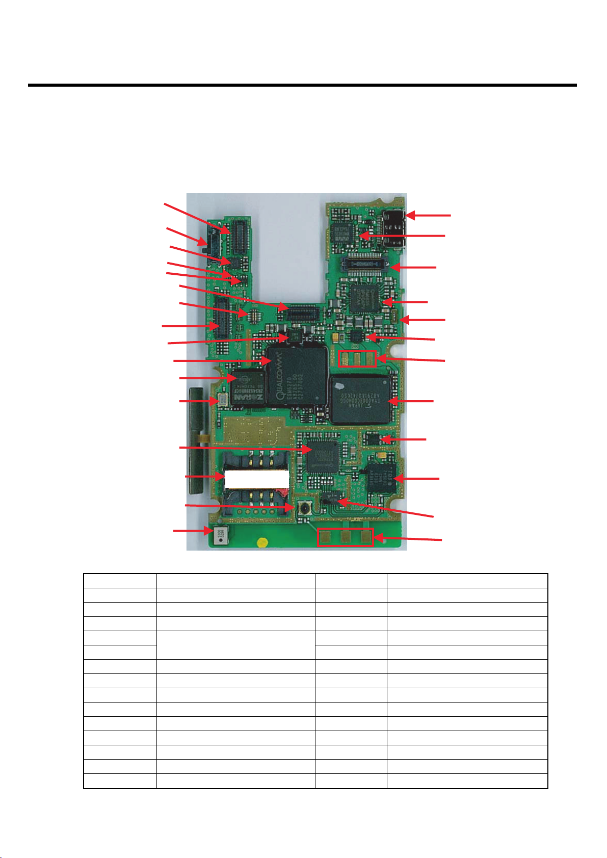
- 77 -
3. TECHNICAL BRIEF
3.14.1.2 Main Bottom Side
LGE Internal Use Only
Copyright © 2008 LG Electronics. Inc. All right reserved.
Only for training and service purposes
Reference Description Reference Description
CN701 Touch FPCB Connector CN500 TA and USB Connector
SW600 Mode Switch U502 WM8983 Audio DAC/ADC AMP IC
U606 Linear Motor Driver IC CN603 Main-Sub B-to-B Connector
U603 U501 PM6635 PMIC
U605 X500 32.768KHz Crystal Oscillator
CN600 5M CAM FPCB Connector U500 Charging IC
CN601 Strobe Flash Connector OUT PAD Battery Connector PAD
CN300 LCD Connector U402 Memory IC
U701 DC-DC Converter IC X100 19.2MHz Crystal Oscillator for TCXO
U200 ESM6270 Modem IC U101 PAM IC for GSM
U302 ZR3453 DSP IC FL100 Antenna Switching Module
X300 27Mhz Crystal Oscillator ANT PAD Main Intenna Connection PAD
U100 RTR6235 RF IC SW100 RF Switch
J400 SIM Connector MIC500 MIC
Linear Motor Control IC
CN701
SW600
U606
U603
U605
CN600
CN601
CN500
U502
CN603
U501
CN300
U701
U200
X500
U500
OUT PAD
U302
X300
U100
J400
U402
X100
U101
SW100
FL100
MIC500
ANT PAD
Page 77

- 78 -
3. TECHNICAL BRIEF
3.14.1.3 Sub PCB
LGE Internal Use Only
Copyright © 2008 LG Electronics. Inc. All right reserved.
Only for training and service purposes
Reference Description Reference Description
BT PAD Bluetooth Antenna PAD SPEAKER Module Speaker
MIC900 CAM MIC S800 T-Flash Connector
U900 U903
U901 U904
U800 Hall IC for Camera Cover Detection CN801 Main-Sub B-to-B Connector
M800 Bluetooth Driver IC BAT900 Backup Battery
U902 Headset Hook Switch IC
5MP Camera Power IC Hall IC for Wheel Switch Detection
BT PAD
MIC900
U903
U900
U901
U902
SPEAKER
U904
U800
S800
M800
BAT900
CN801
Page 78

- 79 -
3. TECHNICAL BRIEF
3.14.1.4 Touch FPCB
LGE Internal Use Only
Copyright © 2008 LG Electronics. Inc. All right reserved.
Only for training and service purposes
Reference Description Reference Description
Vibrator Vibrator PAD
Main B-to-B Connector
Receiver Receiver PAD CN101
(FPCB to Main PCB)
CN102 Touch Window Connector
CN101
CN102
Vibrator
Receiver
Page 79

- 80 -
3. TECHNICAL BRIEF
LGE Internal Use Only
Copyright © 2008 LG Electronics. Inc. All right reserved.
Only for training and service purposes
3.14.1.5 5M Camera FPCB
Reference Description Reference Description
CN601
5M Camera Module
CN602
Main PCB Connector
Connector (FPCB to Main PCB)
CN602
CN601
Page 80

- 81 -
4. TROUBLE SHOOTING
4.1 RF Component
4. TROUBLE SHOOTING
LGE Internal Use Only
Copyright © 2008 LG Electronics. Inc. All right reserved.
Only for training and service purposes
Reference Description Reference Description
U100 GSM Transceiver (RTR) X100 VCTCXO(19.2MHz)
FL100 Front-End-Module U101 GSM/EDGE PAM
SW100 RF Antenna Connector FL101 GSM900 TX SAW
U100
X100
U101
FL100
SW100
FL101
Page 81

- 82 -
4. TROUBLE SHOOTING
4.2 Main Component
4.2.1 GSM PATH
LGE Internal Use Only
Copyright © 2008 LG Electronics. Inc. All right reserved.
Only for training and service purposes
COMMON TX/RX PATH
DCS/PCS TX PA TH
GSM TX PATH
GSM RX PATH
PCS RX PATH
DCS RX PATH
Page 82

- 83 -
4. TROUBLE SHOOTING
LGE Internal Use Only
Copyright © 2008 LG Electronics. Inc. All right reserved.
Only for training and service purposes
4.3 Checking VCTCXO Block
The reference frequency (19.2MHz) from X100 (VCXO) is used UMTS TX part,
GSM part and BB part.
TCXO
0.01u
C141
1000p
C145
X100
2
GNDOUT
3
VCC4VCONT
1
19.2MHz
U102
TC7SH04FS
C144 1000p
0.1u
C139
1000p
C140
100KR120
C147 1000p
C148 8200p
100ohmR115
TRK_LO_ADJVREG_TCXO_2.85V
TCXO_BT
VREG_BT_2.85V
TCXO_PM
RTR6275_TCXO
Schematic of the TCXO Block
Test Point of the TCXO Blcok
TP1 TP2
TP4
TP3
TP1
TP2
TP3
TP4
Page 83

LGE Internal Use Only
Copyright © 2008 LG Electronics. Inc. All right reserved.
Only for training and service purposes
4. TROUBLE SHOOTING
- 84 -
Che
1
VCC o
CXO
VCC
2.8V
Che
2
TRK_LO_AD
3V
olta
g
0V
Che
TP4
th
scil
loscope
19.2
Si
g
nal
VCXO
s OK
Check otot
her part
Che
Che
k MSM
Check
soldering
an
d c
ents
Ye
Ye
No
No
No
Check TP 1
VCC of VCXO
VCC ≥ 2.8V
Check TP 2
TRK_LO_AD J
3V≥Volta e≥0V
Check TP 3, TP4
With Oscil loscope
19.2 MHz Si nal
VCXO is OK
Check ot her part
Check PMIC
Check MSM
Check soldering
and components
Yes
Yes
Yes
No
No
No
TCXO output waveform(19.2MHz)
Che
VCC o
ck k TPTP1
f VCXO
VCC
YeYes
Che
TRK_LO_AD
≥ Volta
3V
Ye
Che
With
19.2
Ye
≥ 2.8V
ck k TPTP2
J
e≥0V
s
ck k TPTP3,3, TP4
Oscil
loscope
MHzHz Si
nal
s
No
No
No
Che
Che
Check
d c
an
ck k PMPMIC
ck MSM
soldering
omponents
is OK
her part
Check
VCXO
Page 84

LGE Internal Use Only
Copyright © 2008 LG Electronics. Inc. All right reserved.
Only for training and service purposes
4. TROUBLE SHOOTING
- 85 -
4.4 Checking Front-End Module Block
Schematic of the Front-End Module Block
Test Point of Front-End Module Block
TP1
TP3
TP2
ANT_SEL0
ANT_SEL1
VREG_RF_SMPS
C113
1000p
C114
1000p
C195
1000p
19
20
21
10
12
13
14
16
18
22
9
VC1
VC2
VDD
GND1
GND2
GND3
GND4
GND5
GND6
GND7
GND8
11
ANT
GSM1800_RX1
GSM1800_RX2
GSM1900_RX1
GSM1900_RX2
GSM1800_1900_TX
NC1
NC2
GSM850_900_TX
LMSP43QA-538
23
24
FL100
GSM850_RX1
GSM850_RX2
GSM900_RX1
GSM900_RX2
1
2
3
4
5
6
7
8
15
17
TP1
TP3
TP2
Page 85

- 86 -
4. TROUBLE SHOOTING
LGE Internal Use Only
Copyright © 2008 LG Electronics. Inc. All right reserved.
Only for training and service purposes
TP3
TP2
TP1
TP2
TP3
TP1
TP2
TP3
TP1
TP2
TP3
TP1
Logic Table of the FEM
DCS1800/PCS1900 Tx
DCS1800 / PCS1900 Rx
GSM900 Tx
GSM900 Rx
Control Logic (L : 0 ~ 0.1V, H : 2.4 ~ 2.8V)
Mode
GSM900 Tx
DCS1800 /PCS1900 Tx
GSM900 Rx
DCS1800 Rx
PCS1900 R
x
TP3
TP1
Vc1
H HH
L H
H L H
L L H
L L H
Vc2 Vd
(V c3)
(V c1)
d
H
TP3
TP1
(V c3)
(V c1)
TP2
TP3
TP1
TP2
(V c2)
(V c3)
(V c1)
(V c2)
TP2
(V c2)
TP3
TP1
(V c3)
(V c1)
TP2
(V c2)
Page 86

- 87 -
4. TROUBLE SHOOTING
Checking Switch Block power source
LGE Internal Use Only
Copyright © 2008 LG Electronics. Inc. All right reserved.
Only for training and service purposes
Check Soldering
ANT_SEL0, 1 High Level
2.5V < Voltgae < 3.0V
YES
Check the Logic
in each mo
de
NO
Check VDD
TP3 VREG_RF_SMPS
Page 87

- 88 -
4. TROUBLE SHOOTING
4.5 Checking GSM Block
4.5.1 Checking Front-End Module
Refer to chapter 3.4
LGE Internal Use Only
Copyright © 2008 LG Electronics. Inc. All right reserved.
Only for training and service purposes
ST A R T
1. C heck Fr ont - E nd
Module Bloc
k
2. C heck RF Tx Leve
3. Check RF Rx L eve
4. Re download SW &
Cali bration
l
l
Page 88
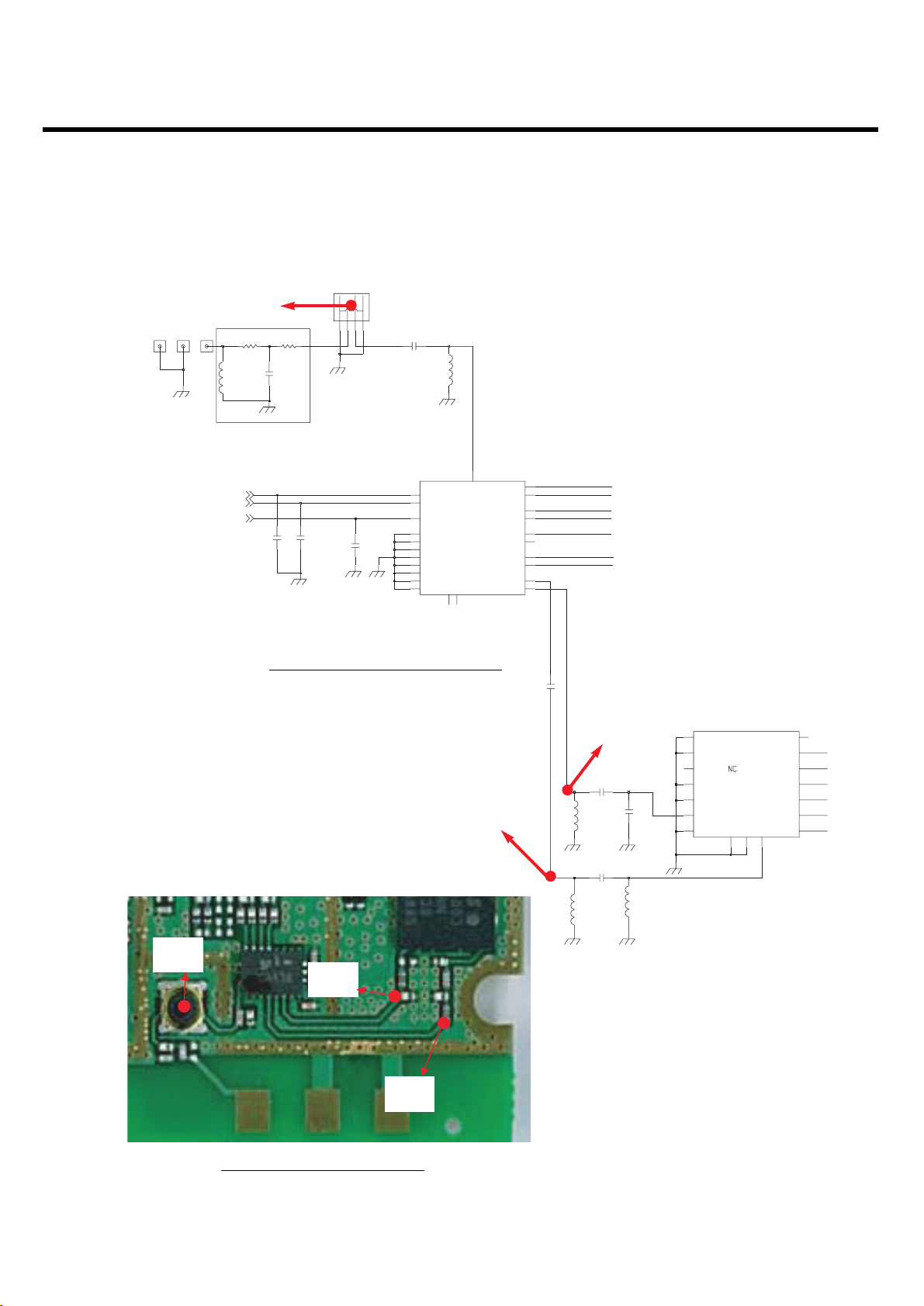
- 89 -
4. TROUBLE SHOOTING
4.5.2 Checking RF Tx Level
LGE Internal Use Only
Copyright © 2008 LG Electronics. Inc. All right reserved.
Only for training and service purposes
Schematic of the GSM Tx Block
Test Point of GSM Tx Block
TP1
TP2
TP3
KMS-518
SW100
ACG1
G2
ANT1000ANT101 ANT102
C102
NA
L100
0
L101
C104
NA
PQ
120pC101
L102
22nH
ANT_SEL0
ANT_SEL1
VREG_RF_SMPS
11
ANT
GSM1800_RX1
GSM1800_RX2
GSM1900_RX1
GSM1900_RX2
GSM1800_1900_TX
NC123NC2
GSM850_900_TX
LMSP43QA-538
24
GSM850_RX1
GSM850_RX2
GSM900_RX1
GSM900_RX2
C113
1000p
C114
1000p
C195
1000p
19
VC1
20
VC2
21
VDD
9
GND1
10
GND2
12
GND3
13
GND4
14
GND5
16
GND6
18
GND7
22
GND8
FL100
1
2
3
4
5
6
7
8
15
17
C717
4.7p
DCS_PCS_IN
TX_EN
VBATT
GND1
VRAMP
DCS_PCS_OUT
GSM_IN
15
1
2
BS
3
4
5
6
7
L112
15nH
C146 2.7p
C142
5.6nH
6.8pC136
C138
NA
L113
5.6nH
14
13
12
11
10
9
8
GND6
GND5
VCC
GND4
GND3
GSM_OUT
GND2
U101
TQM7M5003
GND7
GND8
17
16
TP1
TP2
TP3
Page 89

LGE Internal Use Only
Copyright © 2008 LG Electronics. Inc. All right reserved.
Only for training and service purposes
4. TROUBLE SHOOTING
- 90 -
ST A R T
Check TP1
If GSM over 31 dBm?
If DCS/PCS over 28dBm
Yes
?
GSM /DCS/PCS Tx i s OK
Check other par
t
No
Check TP2, TP3
If TP2 over 29dBm?
If TP3 over 25dBm
Yes
?
Check Fr ont-End
Module
Ref er t o chapter 3.
4
No
s
Check PAM Bl ock OK?
Ref er to chapter 3.5.
3
Ye
Check the R T R623
5
No
Check Soldering of PA M (U101)
If problem still exist,
replace the PA
Pr oblem resol ved
o
N
Change t he Bo ar
M
?
d
Yes
GSM /DCS/PCS Tx i s OK
Page 90

- 91 -
4. TROUBLE SHOOTING
4.5.3 Checking PAM Block
LGE Internal Use Only
Copyright © 2008 LG Electronics. Inc. All right reserved.
Only for training and service purposes
Schematic of PAM Block
Test Point of PAM Block
Test Point Net name Description
TP1 GSM_PA_RAMP Power Amp Gain Control. Typically, 0.2 ~1.6V
TP2 GSM_PA_EN Power Amp Enable (ON : >2.5V, OFF : <0.7V)
TP3 +VPWR PAM Supply Voltage (Vcc > 3V)
TP2
TP1
TP3
14
13
12
11
10
9
8
GND6
GND5
VCC
GND4
GND3
GSM_OUT
GND2
U101
TQM7M5003
GND7
GND8
17
DCS_PCS_IN
DCS_PCS_OUT
16
15
TX_EN
VBATT
GND1
VRAMP
GSM_IN
1
2
BS
3
4
5
6
7
R117 2.2K
C143
68p
GSM_PA_BAND MODE
LOW
HIGH
C137
1u
GSM850/900
DCS/PCS
GSM_PA_BAND
GSM_PA_EN
C135
33u
GSM_PA_RAMP
+VPWR
EFCH836MTDB1
FL101
3
G12G2
IN
1
G3
O1
5
4
R112
R111
68
R113
10 dB
R118
100
R114
10dB
100
68
R119
100
100
DCS_PCS_TX
GSM_TX
TP3
TP1
TP2
Page 91

- 92 -
4. TROUBLE SHOOTING
4.5.4 Checking RF Rx Level
LGE Internal Use Only
Copyright © 2008 LG Electronics. Inc. All right reserved.
Only for training and service purposes
Schematic of GSM-900, DCS-1800, PCS-1900 Rx Block
TP1
TP2
TP3
Test Point of Rx Block
TP1
TP2
TP3
L199 27nH
850GSM
EGSM
19
VC1
20
VC2
21
VDD
9
GND1
10
GND2
12
GND3
13
GND4
14
GND5
16
GND6
18
GND7
22
GND8
11
ANT
GSM1800_RX1
GSM1800_RX2
GSM1900_RX1
GSM1900_RX2
GSM1800_1900_TX
NC123NC2
GSM850_900_TX
LMSP43QA-538
24
GSM850_RX1
GSM850_RX2
GSM900_RX1
GSM900_RX2
1
2
3
4
5
6
7
8
15
17
DCS
PCS
22nH
C719
C718
NA
L198
L109 NA
L111 NA
L105 6.8nH
L108
27nH
6.8nHL103
6.8nHL106
6.8nH
L197
47nH
L110
NA
L104
18nH
L107
12nH
FL100
Page 92
- 93 -
4. TROUBLE SHOOTING
LGE Internal Use Only
Copyright © 2008 LG Electronics. Inc. All right reserved.
Only for training and service purposes
ST A R T
TP1, TP2, TP3
Signals exist
?
No
Rx still has p r o b l e m
N
o
?
Re-download & Calibr atio
Yes
Check Front-End Module
& Soldering of TPs
Yes
GSM -900, DCS-1800, PCS-
1900 Rx is OK
n
Page 93

LGE Internal Use Only
Copyright © 2008 LG Electronics. Inc. All right reserved.
Only for training and service purposes
4.6 Power on trouble
Power on sequence of KE990 is :
PWR key press → PM_ON_SW_N go to low (VA700, PM6635-2M KPDPWR_N pin#24) →
PM6635-2M Power Up → VREG_MSMC_1.2V(C560), VREG_MSME_1.8V(R520),
VREG_MSMP_2.7V(R513), VREG_MSMA_2.6V(R508), VREG_TCXO_2.85V(C510) power
up → PON_RESET_N assert to MSM → Phone booting & PS_HOLD(D500) assert High to
PMIC(PM6635-2M)
4. TROUBLE SHOOTING
- 94 -
Start
Battery volt g. higher
than 3 .2V?
YES
Press PW R key
Keypad L ED on?
YES
VA700 high to lo w
when key press?
YES
VREG_MSMP_2.7V, VREG_MSME
VREG_MSMC_1.2V,
VREG_TCXO_2.85V,
VR
EG_MSMA_2.6V
Power up?
YES
Is c lock ok?
X100 : 19.2M
X500 : 32.768K hz
_1.8V
NO
NO
NO
Change or charging the
Batt ery
Follow the LED trouble
shoot
Check open Pattern
of power button
Check Dome Sheet
NO
Chang e the Main board
NO
Check the TXCO and SLEEP CRYSTAL
Chang e th e Main board
YES
Page 94

LGE Internal Use Only
Copyright © 2008 LG Electronics. Inc. All right reserved.
Only for training and service purposes
4. TROUBLE SHOOTING
- 95 -
VREG_TCXO_2.75V(C510)
VREG_MSMA_2.6V(R508)
VREG_MSMP_2.7V(R513)
SLEEP CRYSTAL(32.768KHz)
VREG_MSMC_1.2V(C560)
VREG_MSME_1.8V(R520)
TCXO ( 19.2MHz )
Page 95
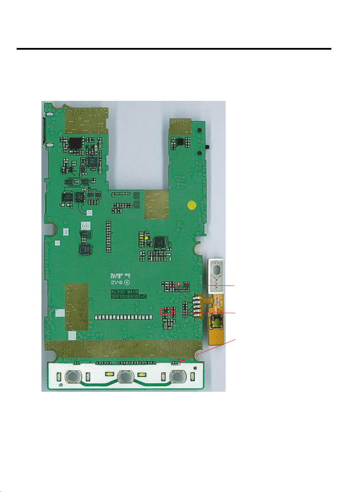
LGE Internal Use Only
Copyright © 2008 LG Electronics. Inc. All right reserved.
Only for training and service purposes
4. TROUBLE SHOOTING
- 96 -
RESET_IN_N(R208)
PS_HOLD(D500)
PM_ON_SW_N (D700)
Page 96

LGE Internal Use Only
Copyright © 2008 LG Electronics. Inc. All right reserved.
Only for training and service purposes
4. TROUBLE SHOOTING
- 97 -
4.6.1 USB trouble
USB Initial sequence of KE990 is :
USB connected to KE990 → USB_VBUS(C540) go to 5V → USB_D+(VA202) go to 3.3V → 48M
Crystal on → USB_DATA is triggered → USB work
Start
Cable is insert?
YES
USB_VBUS i s about
to 5V?
YES
USB_D+ is about to 3. 3V?
YES
48MHz is r un?
YES
Chang e th e Main bo ard
NO
NO
NO
NO
Check C540, R514,U500
Check VA50 0,U507,U304
VA500(USB _D+)
Cable inser t
USB cable
Check X200
X200(48MHz)
R514(USB_VBUS)
C540(USB_VBUS)
U500(USB_VBUS)
U507(USB_D+)
U304(USB_D+)
Page 97

LGE Internal Use Only
Copyright © 2008 LG Electronics. Inc. All right reserved.
Only for training and service purposes
4.6.2 UMS(USB MASS STORAGE) trouble
UMS Initial sequence of KE990 is :
USB connected to KE990 → VREG_5V(R335, UMS) go to 5V → VREG_USB_3.3V(R301) go to 3.3V
→USB_DATA is triggered → USB work
4. TROUBLE SHOOTING
- 98 -
Start
Cable is insert?
YES
VREG_5V is about
to 5V?
YES
VREG_USB_3.3V is
about to 3.3V?
YES
MICRO SD function OK?
YES
Change the Main boar d
NO
Cable inser t
NO
Check R335, D501
NO
Check R301, C529, USB CA BLE
NO
Follow the mi cro sd trouble
< TOP SIDE >
R335(VREG_5V)
C529 (VREG_USB_3.3V)D501(VREG_5V)
R301(VREG_USB_3.3V)
Page 98

4.7 SIM detect trouble
USB Initial sequence of KE990 is :
VREG_SIM_3.0V(C552 of PM6635) go to 3.0V → SIM clock, reset and data triggered → SIM
IF work (Schematic and place are refer to SIM technical brief)
LGE Internal Use Only
Copyright © 2008 LG Electronics. Inc. All right reserved.
Only for training and service purposes
4. TROUBLE SHOOTING
- 99 -
A
Start
Re-inser t th e SIM car d
Work well?
No
VREG_SIM_3.0V is 3.0V?
SIM_P_CLK is run?
YES
Change SIM car d
Work well? End
No
Change th e Main bo ard
Yes
NO
Yes
SIM_P_RST_N
End
Check J40 0, D400,C552
SIM_P_CLK
SIM_P_DAT
C552(VREG_SIM_3.0V)
J400
Page 99

- 100 -
4. TROUBLE SHOOTING
4.8 Key sense trouble (KEYPAD)
Key Sense sequence of KE990 is :
Default condition ROW(0-2) is 2.7V → Press the key → Corresponding ROW(x) and COL(x)
go to 0V → Scan pulse( Col => Row ) → ESM sense what key pressed.
LGE Internal Use Only
Copyright © 2008 LG Electronics. Inc. All right reserved.
Only for training and service purposes
START
Check t he R701,R705,R706 with no ke y p ress
Y
NO
Yes
YE
YE
R710
Check
Chang e th e Main bo ard
S
S
ROW(0-2) is 2.7V?
Yes
Check the R701,R705,R706 wit h ke y press
ROW(0-2),
COL(0-1) is 0V
Chang e th e DOME SHEET
Work w ell?
Chang e SIDE KE
Work w ell?
Check VA700~ VA707, R707~
?
NO
NO
NO
NO
R701,R705,R706
Side Ke y
Chang e th e Main bo ard
Work w ell?
NO
YES
End
Dome sheet
Page 100

- 101 -
4. TROUBLE SHOOTING
LGE Internal Use Only
Copyright © 2008 LG Electronics. Inc. All right reserved.
Only for training and service purposes
Schematic of key sense part
LOCK
SHOT
VA702(COL0)
SEND
VA703(COL1)
VA701(ROW2
)
CLR END
VREG_MSMP_2.7V
KEY_ROW[2]
KEY_COL[0]
KEY_COL[1]
R701
EVLC14S02050VA701
51K
EVLC14S02050VA702
VA703 EVLC14S02050
END
PM_ON_SW_N
701700
CLRSEND
EVL14K02200
END
VA700
ON_SW KEY
VREG_MSMP_2.7V
51K
CN700
EVLC14S02050VA704
R705
EVLC14S02050
EVLC14S02050VA705
VA706
1
2
3
4
5
51K
R706
EVLC14S02050
VA707
R708 470
R709 470
SIDE KEY
470R707
470R710
KEY_ROW[0]
KEY_ROW[1]
KEY_COL[0]
KEY_COL[1]
 Loading...