

lg K500ds Service Manual
MOBILE PHONE
SERVICE MANUAL
CAUTION
BEFORE SERVICING THE UNIT, READ THE “SAFETY PRECAUTIONS” IN THIS MANUAL
MODEL : LG-K500ds
Internal Use Only
Date: April 2016 / Issue 1.0

1. INTRODUCTION................................................. 3
1.1 Purpose
1.2 Regulatory Information
2. PERFORMANCE................................................... 4
2.1 Band Specification
2.2 HW Features
2.3 RSSI Display
2.4 Current consumption
2.5 Battery bar
2.6 SW Specification
3. TROUBLE SHOOTING..........................................12
3.1 Checking XO Block
3.2 Checking Transceiver DC Power Supply Circuit
Block
3.3 Checking DC-DC Block
3.4 ASM(Antenna Switch Module) Block
3.5 GSM RF Part
3.6 WCDMA RF Part
3.7 LTE RF Part
3.8 Power
3.9 Charger
3.10 Audio Block
3.11 Checking LCD Block
3.12 Checking Touch Block
3.13 Checking accelmeter+compass sensor Block
3.14 Checking USB Block
3.15 Checking Main/VT camera Block
3.16 Connectivity RF PART
4. BLOCK DIAGRAM…........................................... 87
5. CIRCUIT DIAGRAM........................................... 96
LGE Internal Use Only
2
Table Of Contents
6. BGA PIN MAP............................................................ 118
7. PCB LAYOUT…........................................................... 119
8. HIDDEN MENU.......................................................... 127
9. DOWNLOAD…........................................................... 130
10. CALIBRATION........................................................... 131
11. DISASSEMBLE GUIDE............................................. 132
12. EXPLODED VIEW………………………………………... 134
13. REPLACEMENT PART LIST..…………………………. 135
Copyright ⓒ 2016 LG Electronics. Inc. All right
reserved. Only training and service purposes
1. INTRODUCTION
3
1.1 Purpose
This manual provides the information necessary to repair, calibration, description and download the features of this model.
1.2 Regulatory Information
A. Security
This material is prohibited to share and release to unauthorized person, in accordance with the regulations, LG Electronics, Civil / criminal
responsibility in accordance with the relevant provisions violate.
B. Precautions for repair
• In case of Disassembly or Assembly
• When using Magnetic tool for the Phone's SVC repair, you should check affect the Electric parts according to effect of Magnet.
• W
hen fastening the screw, be careful not to damage the head of screw and even product.
C. At
tention
Boards, which contain Electrostatic Sensitive Device (ESD), are indicated by the sign.
Following information is ESD handling:
• Service personal should ground themselves by using a wrist, strap when exchange system board.
• When repair are made to a system board, they should spread the floor with anti-static
• Use a suitable, grounded soldering iron.
• Keep sensitive parts in these protective packages until these are used.
• When returning system board or parts like EEPROM to the Factory, use the protective package as described.
LGE Internal Use Only
to repair product, be careful of a product failure caused by RF signals and Static electricity.
mat which is also grounded.
Copyright ⓒ 2016 LG Electronics. Inc. All right
reserved. Only training and service purposes
2.1 Band Specification
4
Support Band TX Freq (MHz) RX Freq (MHz)
LTE(FDD3) 1710 - 1785 1805 - 1880
LTE(FDD7) 2500 - 2570 2620 - 2690
LTE(FDD20) 832 - 862 791 - 821
LTE(TDD38) 2570 - 2620 2570 - 2620
WCDMA(FDD1) 1920 – 1980 2110 – 2170
WCDMA(FDD1) 1850-1910 1930-1990
WCDMA(FDD5) 824 – 849 869 – 894
WCDMA(FDD8) 880 – 915 925 – 960
GSM850 824 – 849 869 – 894
EGSM 880 – 915 925 – 960
DCS1800 1710 – 1785 1805 – 1880
PCS1900 1850 – 1910 1930 – 1990
2. PERFORMANCE
LGE Internal Use Only
Copyright ⓒ 2016 LG Electronics. Inc. All right
reserved. Only training and service purposes
2.2 HW Features
5
List Type / Spec.
1. Phone Type DOP Type
2. Size 142.6 x 71.8 x 7.1 mm
3. Weight 120.0 g ( with Battery )
4. Battery Li-Polymer, 2300mAh
5.Chipset MSM8916 1.2GHz Quad core
6. Memory 16GB(EMMC) + 2MB(LPDDR3) External Memory(SD Card) : Up to 32GB
7. LCD Size 4.93 inch
Display Type Active matrix TFT, Transmissive Type
Color 16.7M colors
2. PERFORMANCE
8. Touch Typ e In-cell Touch
9. Main Camera (13M) Typ e CMOS image sensor
LGE Internal Use Only
Resolution HD+
Resolution 2592(H) X 1944(V) pixels.
Image Scaling Down 5M(2560x1920), W4M(2560x1536)),
3M(1920x1920), 1M(1280x960)
Format Image : JPG, Video : MP4
Copyright ⓒ 2016 LG Electronics. Inc. All right
reserved. Only training and service purposes
2.2 HW Features
6
2. PERFORMANCE
10. Audio
11. Bluetooth Standard Bluetooth 4.1
12. WLAN Standard IEEE 802.11 b/g/n
13. GPS type A-GPS
14. FM type FM Radio, 3.5pi Ear-jack
Receiver 13 X 07 X 2.7T Receiver
Speaker 18 X 10 X 3T Speaker
Format MP3, AAC, MIDI, EAAC+, OGG, AMR
Effective Distance 10M
Distance 0 m ~ 10 m (depend on environment)
Throughput Max 40Mbps (SDIO Driver performance)
Depend on environment 0 ~ 50m (depend on environment)
LGE Internal Use Only
Copyright ⓒ 2016 LG Electronics. Inc. All right
reserved. Only training and service purposes

2.3 RSSI Display
7
2. PERFORMANCE
RSSI BAR
BAR 5->4
BAR 4->3
BAR 3->2
BAR 2->1
BAR 1->0
- 103dBm± 3dB - 101dBm± 3dB -113dBm ±3dB
- 105dBm± 3dB - 107dBm± 3dB -126dBm ± 3dB
2.4 Current consumption
GSM
GSM RSSI
WCDMA RSSI LTE RSSI
- 91dBm± 3dB - 86dBm± 3dB -83dBm ± 3dB
- 96dBm± 3dB - 91dBm± 3dB -93dBm ± 3dB
- 99dBm± 3dB - 97dBm± 3dB -103dBm ± 3dB
Stand by
Tal k
Bluetooth Off Bluetooth On
25 mA 30 mA Under 400 mA
(PP = 5) (PP = 5) (TX Level = Max)
Measurement Co
ndition
LCD Backlight off 370mA
Comment
1. Call Connected &
C
PIPH Level=-3.3
2. LTE: RS
No SVC
Mode
RP
WCDMA
LGE Internal Use Only
LTE
Under 700 mA
25 mA
(DRX = 7)
25 mA 30 mA 350 mA
(DRX = 2.56sec) (DRX = 2.56sec) (Cat 2 Tx= 10dBm)
30 mA
(DRX = 7)
(Max PWR)
Under 250 mA
(TX = 10dBm)
LCD Backlight off 370mA
LCD Backlight off
Copyright ⓒ 2016 LG Electronics. Inc. All right
reserved. Only training and service purposes

2.5 Battery bar
8
Battery Bar Specification Battery Bar Specification
2. PERFORMANCE
Bar 20(Full)
98% ↑
Bar 9 -> Bar 8
43% -> 42%
Bar 20 -> Bar 19
Bar 19 -> Bar 18
98% -> 97%
93% -> 92%
Bar 8 -> Bar 7
Bar 7 -> Bar 6
38% -> 37%
33% -> 32%
Bar 18 -> Bar 17
Bar 17 -> Bar 16
88% -> 87%
83% -> 82%
Bar 6 -> Bar 5
Bar 5 -> Bar 4
28% -> 27%
23% -> 22%
Bar 16 -> Bar 15
Bar 15 -> Bar 14
Bar 14 -> Bar 13
Bar 13 -> Bar 12
Bar 12 -> Bar 11
78% -> 77%
73% -> 72%
68% -> 67%
63% -> 62%
58% -> 57%
Bar 4 -> Bar 3
Bar 3 -> Bar 2
Bar 2 -> Bar 1
Bar 1 -> Bar 0
Power off
16% -> 15%
13% -> 12%
8% -> 7%
3% -> 2%
2% -> 1%
Bar 11 -> Bar 10
Bar 10 -> Bar 9
LGE Internal Use Only
53% -> 52%
48% -> 47%
Low battery pop-up
15% , 5%
Copyright ⓒ 2016 LG Electronics. Inc. All right
reserved. Only training and service purposes

2. PERFORMANCE
[German, Spanish(Spain, Argentina, Bolivia,
), Swedish, Russian, English,
9
2.6 SW Specification
Item Feature Comment
RSSI 0 ~ 5 Levels
Battery Charging 0 ~ 20 Levels
Ke y Vol ume 0 ~ 7 Level ringtone, notification, system, call volume
Audio Volume 0 ~ 15 Level music, video, games & other media
Time / Date Display Yes
Multi-Language Ye s Support total 35 languages
Chile, Colombia, Costa Rica, Dominican Re
public, Ecuador, El Salvador, Guatemala, H
onduras, Mexico, Nicaragua, Panama, Para
guay, Peru, Puerto Rico, Español(Estados U
nidos), Uruguay, Venezuela)
, French, Italian, Dutch, Polish, Portuguese(
Por tugal, Brasil
Arabic, Chinese Simlified, Korean, Japanese
Quick Access Mode Phone/Applications/Browser/Messaging
PC Sync Yes
Speed Dial Yes Voice mail center -> 1 key
Profile Yes not same with feature phone setting
CLIP / CLIR Yes
Phone Book Name / Number / Email / Groups / Postal address
es / Organizations / IM / Note / Nickname / Webs
ite / Event /
Last Dial Number Yes Call histories are displayed in chronologica
Last Received Number Yes Call histories are displayed in chronologica
Last Missed Number Yes Call histories are displayed in chronologica
Search by Number/Name Yes
There is no limitation on the number of it
It depends on available memory amount.
.]
ems.
l order
l order
l order
LGE Internal Use Only
Group Yes There is no limitation on the number of it
ems.
It depends on available memory amount.
Fixed Dial Number Yes
Service Dial Number Ye s
Own Number Yes My Profile (add/edit/delete are supported
)
Voice Memo Yes Support voice recorder
Copyright ⓒ 2016 LG Electronics. Inc. All right
reserved. Only training and service purposes

2.6 SW Specification
10
EMS Melody / Picture
Send / Receive / Save
Send / Receive / Save
2. PERFORMANCE
Call Reminder No
Network Selection Automatic
Mute Yes
Call Divert Yes
Call Barring Yes
Call Charge (AoC) No
Call Duration Yes
SMS (EMS)
SMS Over GPRS Yes
MMS MPEG4
Long Message MAX 2000 characters The standard of Open vender
Cell Broadcast Ye s
Download Over the Web
Game No
Calendar Yes
Memo Ye s
There is no limitation on the number of items.
It depends on available memory amount.
No EMS does not support
Yes
There is no limitation on the number of i
It depends on available memory amount
EMS does not support.
tems.
.
LGE Internal Use Only
World Clock Yes
Unit Convert No
Stop Watch Yes
Wall Paper Yes
WAP Browser No
Support only web browser based on we
bkit. WAP stack and wml are not support
ed.
Copyright ⓒ 2016 LG Electronics. Inc. All right
reserved. Only training and service purposes
2.6 SW Specification
AP, OPP, MAP, HID, PAN, HOGP, HDP
11
Download Melody /
Wallpaper
SIM Lock Yes
SIM Toolkit Ye s
Camera Ye s
Voice Dial No
Bluetooth Yes
FM radio Ye s
Hold / Retrieve Yes
Conference Call Yes Max. 6
Memo pad No
SyncML No
2. PERFORMANCE
Yes Over web browser
MMS Yes OMA MMS 1.2 version
EONS Yes
CPHS Yes V4.2
ENS No
13M AF / 8MP
Digital Zoom : x4
JAVA No
IrDa No
Ver. 4.0 [HSP, HFP, A2DP, AVRCP, PB
, DID]
GPRS Yes Class 12
EDGE Yes Class 12
DTMF Ye s
TTY No
AMR Yes
IM Yes Google Hangout
Email Yes IMAP/POP3/EAS
LGE Internal Use Only
Copyright ⓒ 2016 LG Electronics. Inc. All right
reserved. Only training and service purposes
3. TROUBLE SHOOTING
12
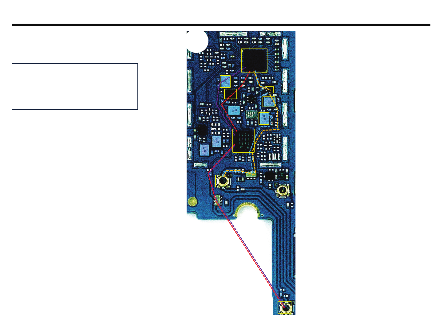
3.1 Checking XO Block
The out put frequency(26MHz) of shared clock from PMIC(U4100) is used as the reference one of WTR4905-1
TP1
Checking Flow Image
START
Check TP1
Is it 26MHz?
NO
Replace U4100 and then
check TP1
Is it 26MHz?
NO
The Problem may be
Logic part
Refer to Logic trouble shoot
YES
YES
Main
BOT
U1500
XO Circuit is OK.
Check next step
XO Circuit is OK.
Check next step
Circuit Diagram
LGE Internal Use Only
TP1
Copyright ⓒ 2016 LG Electronics. Inc. All right
reserved. Only training and service purposes

3.2 Checking Transceiver DC Power Supply Circuit Block
13
The WTR4905-1 operating voltages used two voltage sources 1.22V and 2.05V
Checking Flow Image
START
Main
BOT
3. TROUBLE SHOOTING
TP1
Check TP1
+2.05V_RF is OK?
YES
Check TP2
+1.22V_RF is OK?
YES
Check next step
NO
NO
The Problem may be Logic part
Refer to Logic trouble shoot
The Problem may be Logic part
Refer to Logic trouble shoot
Circuit Diagram
TP2
U1500
TP2
TP1
LGE Internal Use Only
Copyright ⓒ 2016 LG Electronics. Inc. All right
reserved. Only training and service purposes
3. TROUBLE SHOOTING
14
3.3 Checking DC-DC Block
The APT, PMIC(U1400, U4100) output voltages is used as the reference one of SKY77660-21
START
Check TP1
0.5V ≤ TP2 ≤ 4.2V ?
YES
Check TP2
Is VPWR OK?
YES
Check next step
Main
Bot
Checking Flow
Damage or soldering condition
NO
Damage or soldering condition
NO
Image
U1400
Check U1400 Physical
Check U4100 Physical
Circuit Diagram
TP1
TP2
LGE Internal Use Only
TP1
TP2
Copyright ⓒ 2016 LG Electronics. Inc. All right
reserved. Only training and service purposes

3.4 ASM(Antenna Switch Module) Block
15
Checking ANT ASM (GSM,WCDMA,LTE)
Checking Flow
3. TROUBLE SHOOTING
START
Check
TP1, TP2 High Level ?
(1.5V≤TP1 ≤2.1V)
(2.5V≤TP2 ≤3.1V)
YES
Check
U1200 physical Damage
or soldering condition
OK?
Check Next step
Main
BOT
NO
NOT GOOD
Image
U1200
Circuit Diagram
The Problem may be
Logic part
Refer to Logic trouble
shoot
TP2
Replace U1200
TP1
LGE Internal Use Only
TP2
TP1
Copyright ⓒ 2016 LG Electronics. Inc. All right
reserved. Only training and service purposes
3. TROUBLE SHOOTING
16
3.5 GSM RF PART
GSM RF Part support GSM850/900/1800/1900 with ASM, PAM, Transceiver component
Checking Flow
START
Check XO Block
Refer 3.1
Check Transceiver DC Power supply Block
Refer 3.2
Check DC-DC Block
Refer 3.3
LGE Internal Use Only
Check ASM Block
Refer 3.4
Check T/RX Block
Re-Download & Cal
Change the Board
Copyright ⓒ 2016 LG Electronics. Inc. All right
reserved. Only training and service purposes
3. TROUBLE SHOOTING
17
3.5 GSM RF PART
3.5.1 GSM RF Part RX RF PATH
1. GSM850 RX PATH
2. GSM900 RX PATH
3. GSM1800 RX PATH
4. GSM1900 RX PATH
Main
BOT
U1500
U1200
SW1001
LGE Internal Use Only
SW1000
Copyright ⓒ 2016 LG Electronics. Inc. All right
reserved. Only training and service purposes

3.5 GSM RF PART
18
3.5.2 Checking RF Signal RX path(SW, GSM850/900)
Checking Flow
START
3. TROUBLE SHOOTING
Image
U1200
Check TP1 Signal exist?
YES
Check TP2 Signal exist?
YES
Check next step
TP1
NO
NO
Check SW1000
Soldering
Check U1200
Soldering
TP1
Circuit Diagram
TP2
(For GSM850)
TP2
(For GSM900)
TP2
(For GSM850)
LGE Internal Use Only
TP2
(For GSM900)
Copyright ⓒ 2016 LG Electronics. Inc. All right
reserved. Only training and service purposes

3.5 GSM RF PART
19
3.5.3 Checking RF Signal RX path(GSM850/900)
Checking Flow Image
START
Check Component
Check TP1/2 Signal exist?
NO
YES
GSM850 – FL1200
GSM900 – Fl1201
3. TROUBLE SHOOTING
Check Transceiver
physical damage
or soldering condition
Check next step
LGE Internal Use Only
OK?
NOT GOOD
TP2
Replace U1500
Circuit Diagram
TP1
TP2
(For GMS900)
TP1
(For GMS850)
Copyright ⓒ 2016 LG Electronics. Inc. All right
reserved. Only training and service purposes

3.5 GSM RF PART
20
3.5.4 Checking RF Signal RX path(SW, GSM1800/1900)
3. TROUBLE SHOOTING
Checking Flow
START
Check TP1 Signal exist?
YES
Check TP2 Signal exist?
YES
Check next step
TP2
(For GSM1900)
NO
NO
Check SW1001
Soldering
Check U1200
Soldering
U1200
Circuit Diagram
TP1
Image
TP2
(For GSM1900)
TP2
(For GSM1800)
LGE Internal Use Only
TP1
TP2
(For GSM1800)
Copyright ⓒ 2016 LG Electronics. Inc. All right
reserved. Only training and service purposes

3.5 GSM RF PART
21
3.5.5 Checking RF Signal RX path(GSM1800/1900)
Checking Flow
START
Check Component
Check TP1/2 Signal exist?
NO
YES
GSM1900 – FL1205
GSM1800 – FL1208
3. TROUBLE SHOOTING
Image
TP3
TP2
(For GMS1800)
TP1
(For GMS1900)
LGE Internal Use Only
Check TP3 Signal exist?
YES
Check Transceiver
physical damage
or soldering condition
OK?
Check next step
NO
NOT GOOD
CheckU1201Soldering
Replace U1500
Circuit Diagram
TP1
TP3
TP2
Copyright ⓒ 2016 LG Electronics. Inc. All right
reserved. Only training and service purposes

3. TROUBLE SHOOTING
22
3.5 GSM RF PART
3.5.6 GSM RF Part TX RF PATH
1. GSM850/900 TX PATH
2. GSM1800/1900 TX PATH
Main
BOT
Main
TOP
U1400
U1200
SW1001
LGE Internal Use Only
SW1000
Copyright ⓒ 2016 LG Electronics. Inc. All right
reserved. Only training and service purposes

3.5 GSM RF PART
23
3. TROUBLE SHOOTING
3.5.7 Checking RF Signal TX path(SW, GSM LB/HB)
Checking Flow
START
Check TP1 Signal exist?
YES
Check TP2 Signal exist?
YES
Check Soldering
NO
NO
HB: SW1001
LB: SW1000
Check U1200
Soldering
TP1
(For GSM850/900)
U1200
TP1
(For GSM1800/1900)
Circuit Diagram
Image
U1400
TP2
TP2
(For GSM1800/1900)
(For GSM850/900)
Check Transceiver
physical damage
or soldering condition
Check next step
LGE Internal Use Only
NOT GOOD
Replace U1400
TP1
(For GSM1800/1900)
TP1
(For GSM850/900)
TP2
(For GSM1800/1900)
TP2
(For GSM850/900)
Copyright ⓒ 2016 LG Electronics. Inc. All right
reserved. Only training and service purposes

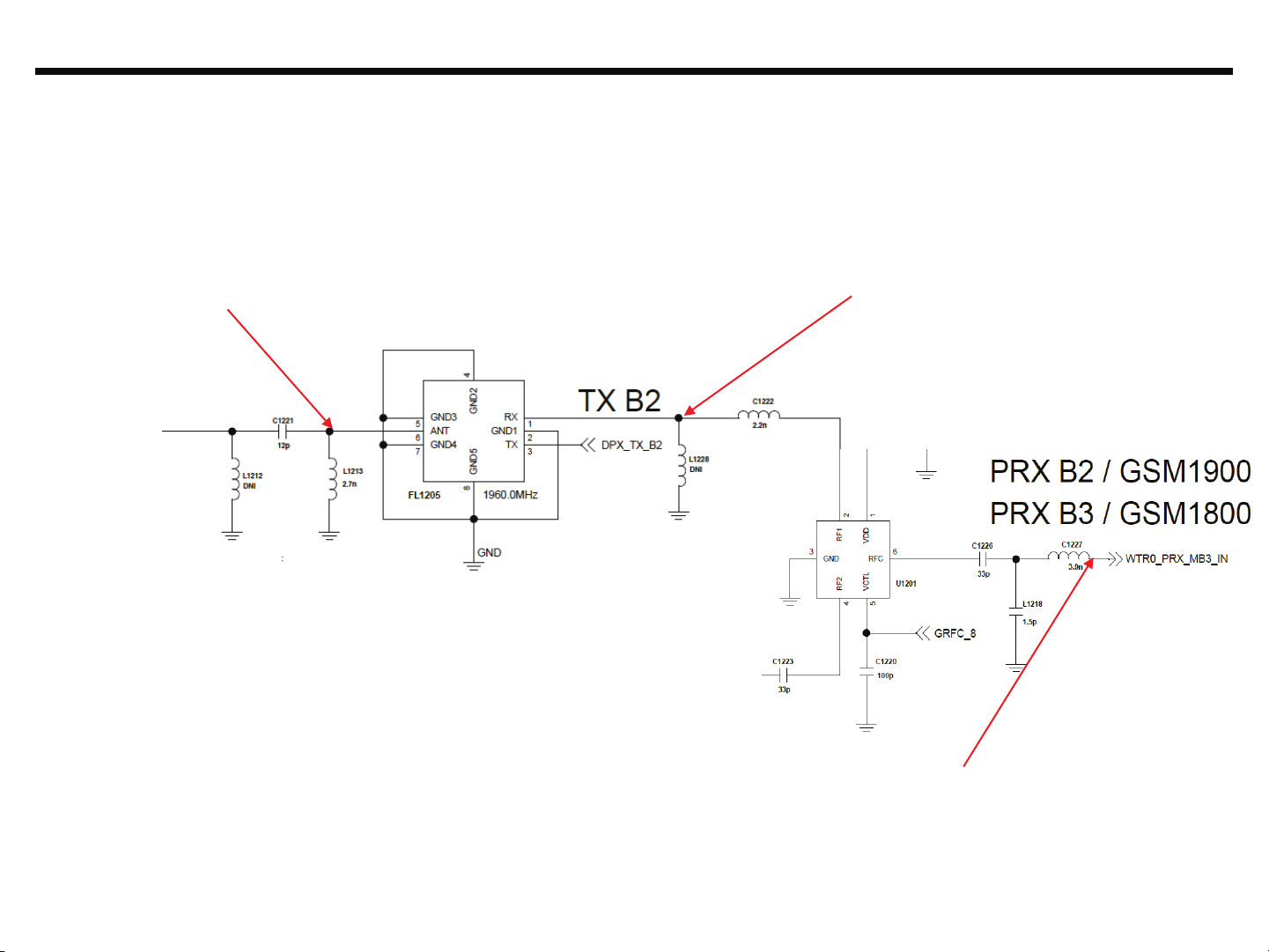
3.6 WCDMA RF PART
24
WCDMA RF Part support WCDMA B1/2/5/8 with ASM, PAM, Transceiver component
Checking Flow
START
Check XO Block
Refer 3.1
Check Transceiver DC Power supply Block
Refer 3.2
Check DC-DC Block
Refer 3.3
3. TROUBLE SHOOTING
LGE Internal Use Only
Check ASM Block
Refer 3.4
Check T/RX Block
Re-Download & Cal
Change the Board
Copyright ⓒ 2016 LG Electronics. Inc. All right
reserved. Only training and service purposes
3.6 WCDMA RF PART
25
3.6.1 WCDMA RF Part RX RF PATH
1. WCDMA B1 RX PATH
2. WCDMA B2 RX PATH
3. WCDMA B1/2 COMMON PATH
4. WCMDA B5 RX PATH
5. WCMDA B8 RX PATH
6. WCMDA B5/8 COMMON PATH
3. TROUBLE SHOOTING
Main
BOT
LGE Internal Use Only
Copyright ⓒ 2016 LG Electronics. Inc. All right
reserved. Only training and service purposes

3.6 WCDMA RF PART
26
3.6.2 Checking RF Signal RX path(SW, WCDMA B1/B2)
Checking Flow
START
3. TROUBLE SHOOTING
Image
Main
Bot
Check TP1 Signal exist?
YES
Check TP2 Signal exist?
YES
Check next step
NO
NO
Check SW1001
Soldering
Check FL1002
Soldering
TP1
TP1
TP2
SW1001
FL1002
Circuit Diagram
LGE Internal Use Only
TP2
Copyright ⓒ 2016 LG Electronics. Inc. All right
reserved. Only training and service purposes
3.6 WCDMA RF PART
27
3. TROUBLE SHOOTING
3.6.3 Checking RF Signal RX path(WCDMA B1)
Checking Flow
START
Check TP1 Signal exist?
YES
Check TP2 Signal exist?
YES
Check TP3 Signal exist?
YES
NO
NO
NO
Replace U1200
Check FL1207 Soldering
and Check Component
above RF signal path
Check U1208 Soldering and
Check Component
above RF signal path
TP3
TP1
Image
Main
Bot
U1500
U1208
FL1207
U1200
TP2
Check Transceiver
physical damage
or soldering condition
Check next step
LGE Internal Use Only
Replace U1500
NOT GOOD
OK?
Copyright ⓒ 2016 LG Electronics. Inc. All right
reserved. Only training and service purposes
3.6 WCDMA RF PART
28
3.6.3 Checking RF Signal RX path(WCDMA B1)
TP1
3. TROUBLE SHOOTING
Circuit Diagram
LGE Internal Use Only
TP2
TP3
Copyright ⓒ 2016 LG Electronics. Inc. All right
reserved. Only training and service purposes
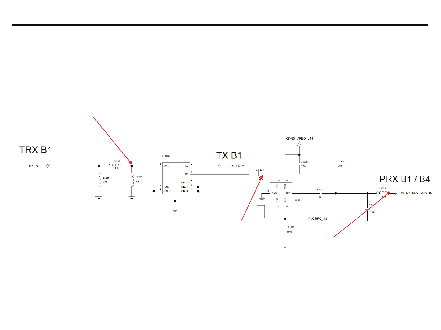
3.6 WCDMA RF PART
29
3.6.3 Checking RF Signal RX path(WCDMA B2)
Checking Flow
START
Check TP1 Signal exist?
YES
NO
Replace U1200
Main
Bot
3. TROUBLE SHOOTING
Image
TP3
U1500
Check TP2 Signal exist?
Check TP3 Signal exist?
Check Transceiver
physical damage
or soldering condition
Check next step
LGE Internal Use Only
YES
YES
OK?
NO
NO
NOT GOOD
Check FL1205 Soldering
and Check Component
above RF signal path
Check U1201 Soldering and
Check Component
above RF signal path
Replace U1500
U1201
TP2
FL1205
U1200
TP1
Copyright ⓒ 2016 LG Electronics. Inc. All right
reserved. Only training and service purposes
3.6 WCDMA RF PART
30
3.6.3 Checking RF Signal RX path(WCDMA B2)
TP1
3. TROUBLE SHOOTING
Circuit Diagram
TP2
LGE Internal Use Only
TP3
Copyright ⓒ 2016 LG Electronics. Inc. All right
reserved. Only training and service purposes
 Loading...