

Page 1
DVB-T/HDD/DVD RECORDER
SERVICE MANUAL
MODELS : HDR899/1000
CAUTION
BEFORE SERVICING THE UNIT, READ THE “SAFETY PRECAUTIONS”
IN THIS MANUAL.
MODELS : HDR899/1000
SERVICE MANUAL
Website http://biz.lgservice.com
Internal Use Only
Page 2

CONTENTS
SECTION 1.........SUMMARY
SECTION 2.........CABINET & MAIN CHASSIS
SECTION 3.........ELECTRICAL
SECTION 4.........RS-06A LOADER PART
SECTION 5.........REPLACEMENT PARTS LIST
Copyright © 2008 LG Electronics. Inc. All right reserved.
Only for training and service purposes
LGE Internal Use Only
Page 3

SECTION 1
SUMMARY
CONTENTS
NEW FUNCTIONS OF HDD/DVD RECORDER .................................................................................1-3
PRODUCT SAFETY SERVICING GUIDELINES FOR HDD/DVD RECORDER PRODUCTS
SERVICING PRECAUTIONS....................................................................................................................1-5
• GENERAL SERVICING PRECAUTIONS
• INSULATION CHECKING PRODEDURE
• ELECTROSTATICALLY SENSITIVE (ES) DEVICES
SERVICE INFORMATION FOR EEPROM IC SETTING..................................................................1-6
UPGRADE THE MAIN & LOADER PROGRAM.................................................................................1-7
SPECIFICATIONS ........................................................................................................................................1-8
..............1-4
LGE Internal Use Only
1-2
Copyright © 2008 LG Electronics. Inc. All right reserved.
Only for training and service purposes
Page 4

NEW FUNCTIONS OF HDD/DVD RECORDER
• HDMI
HDMI IS THE SPECIFICATION FOR THE HIGH-DEFINITION MULTIMEDIA INTERFACE. HDMI IS PROVIDED
FOR TRANSMITTING DIGITAL TELEVISION AUDIOVISUAL SIGALS FROM HDD-DVD RECODER TO TELEVISION SETS, OTHER VIDEO DISPLAYS. HDMI CAN CARRY HIGH QUALITY MULTI-CHANNEL AUDIO DATA
AND CAN CARRY ALL STANDARD AND HIGH DEFINITION CONSUMER ELECTRONICS VIDEO FORMATS.
CONTENT PROTECTION TECHNOLOGY IS AVAILABLE. HDMI CAN ALSO CARRY CONTROL AND STATUS
INFORMATION IN BOTH DIRECTIONS.
<< OPERATING >>
AUDIO, VIDEO AND AUXILIARY DATA IS TRANSMITTED ACROSS THE THREE TMDS DATA CHANNELS.
THE VIDEO PIXEL CLOCK IS TRANSMITTED ON THE TMDS CLOCK CHANNEL AND USED BY THE
RECEIVER AS A FREQUENCY REFERENCE FOR DATA RECOVERY ON THE THREE TMDS DATA CHANNELS.
VIDEO DATA IS CARRIED AS A SERIES OF 24-BIT PIXELS ON THE THREE TMDS DATA CHANNELS.
TMDS ENCODING CONVERTS THE 8BIT PER CHANNEL INTO THE 10BIT DC-BALANCED.
VIDEO PIXEL RATES CAN RANGE FROM 25MHz TO 165MHz. THE VIDEO PIXELS CAN BE ENCODED IN
EITHER RGB, YCbCr 4:4:4 OR YCbCr 4:2:2 FORAMTS. IN ALL THREE CASES, UP TP 24 BITS PER PIXEL
CAN BE TRANSFERRED.
FAST DUBBING
DUBBING MEANS A COPYING FUNCTION BETWEEN HDD TO DVD DISCS.
COPYING BETWEEN HDD TO DVD IS A COMPLETELY DIGITAL PROCESS AND THEREFORE INVOLVES
NO LOSS OF QUALITY IN THE AUDIO OR VIDEO. SO THIS MEANS THAT COPYING CAN BE CARRIED OUT
AT THE MAXIMUM SPEED POSSIBLE.
<< DUBBING SPEED RATE >>
NORMAL DUBBING : SPEED RATE MAX X1
FAST DUBBING : SPEED RATE MAX X4
WHEN FAST DUBBING FROM HDD TO DVD, THE SPEED OF COPYING DEPENDS ON THE RECODING
MODE AND THE KIND OF USING THE DVD DISC, AND THIS MODE IS NOT AVAILABLE FOR EDITED VIDEO
TITLE IN HDD.
WHEN FAST DUBBING FROM DVD TO HDD, ONLY AVAILABLE WHEN COPYING VR MODE DISC(DVD-RW)
TO HDD, AND ONLY NORMAL DUBBING AVAILABLE WHEN COPYING VIDEO MODE DISC(DVD+RW/RW,
DVD-R) TO HDD.
Copyright © 2008 LG Electronics. Inc. All right reserved.
Only for training and service purposes
1-3
LGE Internal Use Only
Page 5
PRODUCT SAFETY SERVICING GUIDELINES FOR HDD/DVD RECORDER PRODUCTS
IMPORTANT SAFETY NOTICE
This manual was prepared for use only by properly trained audio-video service technicians.
When servicing this product, under no circumstances should the original design be
modified or altered without permission from LG Corporation. All components should
be replaced only with types identical to those in the original circuit and their physical
location, wiring and lead dress must conform to original layout upon completion of
repairs.
Special components are also used to prevent x-radiation, shock and fire hazard.
These components are indicated by the letter “x” included in their component designators and are required to maintain safe performance. No deviations are allowed
without prior approval by LG Corporation.
Circuit diagrams may occasionally differ from the actual circuit used. This way, implementation of the latest safety and performance improvement changes into the set is
not delayed until the new service literature is printed.
CAUTION
tomized installations without manufacturer’s approval. Unauthorized modifications will
not only void the warranty, but may lead to property damage or user injury.
Service work should be performed only after you are thoroughly familiar with these
safety checks and servicing guidelines.
: Do not attempt to modify this product in any way. Never perform cus-
GRAPHIC SYMBOLS
The exclamation point within an equilateral triangle is intended to alert
the service personnel to important safety information in the service literature.
The lightning flash with arrowhead symbol within an equilateral triangle is intended to alert the service personnel to the presence of noninsulated “dangerous voltage” that may be of sufficient magnitude to
constitute a risk of electric shock.
The pictorial representation of a fuse and its rating within an equilateral triangle is intended to convey to the service personnel the following
fuse replacement caution notice:
CAUTION : FOR CONTINUED PROTECTION AGAINST RISK OF
FIRE, REPLACE ALL FUSES WITH THE SAME TYPE AND RATING AS MARKED NEAR EACH FUSE.
SERVICE INFORMATION
While servicing, use an isolation transformer for protection from AC line shock. After
the original service problem has been corrected, make a check of the following:
FIRE AND SHOCK HAZARD
1. Be sure that all components are positioned to avoid a possibility of adjacent component shorts. This is especially important on items trans-ported to and from the
repair shop.
2. Verify that all protective devices such as insulators, barriers, covers, shields, strain
reliefs, power supply cords, and other hardware have been reinstalled per the original design. Be sure that the safety purpose of the polarized line plug has not been
defeated.
3. Soldering must be inspected to discover possible cold solder joints, solder splashes, or sharp solder points. Be certain to remove all loose foreign particles.
4. Check for physical evidence of damage or deterioration to parts and components,
for frayed leads or damaged insulation (including the AC cord), and replace if necessary.
5. No lead or component should touch a high current device or a resistor rated at 1
watt or more. Lead tension around protruding metal surfaces must be avoided.
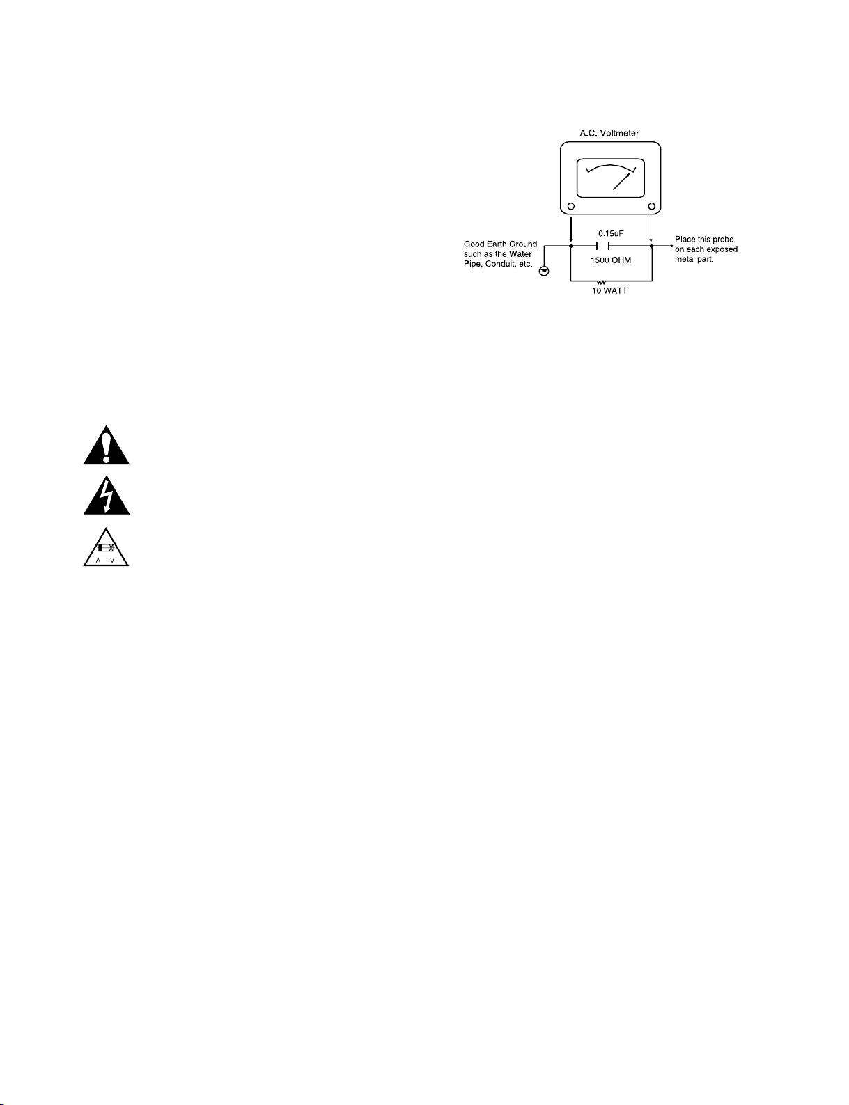
6. After reassembly of the set, always perform an AC leakage test on all exposed
metallic parts of the cabinet (the channel selector knobs, antenna terminals, handle and screws) to be sure that set is safe to operate without danger of electrical
shock. DO NOT USE A LINE ISOLATION TRANSFORMER DURING THIS
TEST. Use an AC voltmeter having 5000 ohms per volt or more sensitivity in the
following manner: Connect a 1500 ohm, 10 watt resistor, paralleled by a .15 mfd
150V AC type capacitor between a known good earth ground water pipe, conduit,
etc.) and the exposed metallic parts, one at a time. Measure the AC voltage across
the combination of 1500 ohm resistor and .15 mfd capacitor. Reverse the AC plug
by using a non-polarized adaptor and repeat AC voltage measurements for each
exposed metallic part. Voltage measured must not exceed 0.75 volts RMS. This
corresponds to 0.5 milliamp AC. Any value exceeding this limit constitutes a potential shock hazard and must be corrected immediately.
TIPS ON PROPER INSTALLATION
1. Never install any receiver in a closed-in recess, cubbyhole, or closely fitting shelf
space over, or close to, a heat duct, or in the path of heated air flow.
2. Avoid conditions of high humidity such as: outdoor patio installations where dew
is a factor, near steam radiators where steam leakage is a factor, etc.
3. Avoid placement where draperies may obstruct venting. The customer should also
avoid the use of decorative scarves or other coverings that might obstruct ventilation.
4. Wall- and shelf-mounted installations using a commercial mounting kit must follow
the factory-approved mounting instructions. A product mounted to a shelf or platform must retain its original feet (or the equivalent thickness in spacers) to provide
adequate air flow across the bottom. Bolts or screws used for fasteners must not
touch any parts or wiring. Perform leakage tests on customized installations.
5. Caution customers against mounting a product on a sloping shelf or in a tilted position, unless the receiver is properly secured.
6. A product on a roll-about cart should be stable in its mounting to the cart.
Caution the customer on the hazards of trying to roll a cart with small casters
across thresholds or deep pile carpets.
7. Caution customers against using extension cords. Explain that a forest of extensions, sprouting from a single outlet, can lead to disastrous consequences to
home and family.
LGE Internal Use Only
1-4
Copyright © 2008 LG Electronics. Inc. All right reserved.
Only for training and service purposes
Page 6

SERVICING PRECAUTIONS
CAUTION: Before servicing the HDD / DVD RECORDER covered by this service data and its supplements and addends,
read and follow the SAFETY PRECAUTIONS. NOTE: if
unforeseen circumstances create conflict between the following servicing precautions and any of the safety precautions in
this publications, always follow the safety precautions.
Remember Safety First :
General Servicing Precautions
1. Always unplug the HDD / DVD RECORDER AC power cord
from the AC power source before:
(1) Removing or reinstalling any component, circuit board,
module, or any other assembly.
(2) Disconnecting or reconnecting any internal electrical
plug or other electrical connection.
(3) Connecting a test substitute in parallel with an electrolyt-
ic capacitor.
Caution : A wrong part substitution or incorrect polarity
installation of electrolytic capacitors may result in an
explosion hazard.
2. Do not spray chemicals on or near this HDD / DVD
RECORDER or any of its assemblies.
3. Unless specified otherwise in this service data, clean electrical contacts by applying an appropriate contact cleaning
solution to the contacts with a pipe cleaner, cotton-tipped
swab, or comparable soft applicator.
Unless specified otherwise in this service data, lubrication of
contacts is not required.
4. Do not defeat any plug/socket B+ voltage interlocks with
whitch instruments covered by this service manual might be
equipped.
5. Do not apply AC power to this HDD / DVD RECORDER and
/ or any of its electrical assemblies unless all solidstate
device heat sinks are correctly installed.
6. Always connect the test instrument ground lead to an appropriate ground before connecting the test instrument positive
lead. Always remove the test instrument ground lead last.
Electrostatically Sensitive (ES) Devices
Some semiconductor (solid state) devices can be damaged
easily by static electricity. Such components commonly are
called Electrostatically Sensitive (ES) Devices. Examples of
typical ES devices are integrated circuits and some field effect
transistors and semiconductor chip components.
The following techniques should be used to help reduce the
incidence of component damage caused by static electricity.
1. Immediately before handling any semiconductor component
or semiconductor-equipped assembly, drain off any electrostatic charge on your body by touching a known earth
ground. Alternatively, obtain and wear a commercially available discharging wrist strap device, which should be
removed for potential shock reasons prior to applying power
to the unit under test.
2. After removing an electrical assembly equipped with ES
devices, place the assembly on a conductive surface such
as aluminum foil, to prevent electrostatic charge buildup or
exposure of the assembly.
3. Use only a grounded-tip soldering iron to solder or unsolder
ES devices.
4. Use only an anti-static solder removal device. Some solder
removal devices not classified as “anti-static” can generate
electrical charges sufficient to damage ES devices.
5. Do not use freon-propelled chemicals. These can generate
an electrical charge sufficient to damage ES devices.
6. Do not remove a replacement ES device from its protective
package until immediately before you are ready to install it.
(Most replacement ES devices are packaged with leads
electrically shorted together by conductive foam, aluminum
foil,or comparable conductive material).
7. Immediately before removing the protective material from
the leads of a replacement ES device, touch the protective
material to the chassis or circuit assembly into which the
device will be installed.
Insulation Checking Procedure
Disconnect the attachment plug from the AC outlet and turn
the power on. Connect an insulation resistance meter (500V)
to the blades of the attachment plug. The insulation resistance
between each blade of the attachment plug and accessible
conductive parts (Note 1) should be more than 1Mohm.
Note 1 : Accessible Conductive Parts include Metal panels,
Input terminals, Earphone jacks,etc.
Copyright © 2008 LG Electronics. Inc. All right reserved.
Only for training and service purposes
Caution: Be sure no power is applied to the chassis or circuit, and observe all other safety precautions.
8. Minimize bodily motions when handling unpackaged
replacement ES devices. (Normally harmless motion such
as the brushing together of your clothes fabric or the lifting
of your foot from a carpeted floor can generate static electricity sufficient to damage an ES device.)
1-5
LGE Internal Use Only
Page 7
SERVICE INFORMATION FOR EEPROM IC SETTING
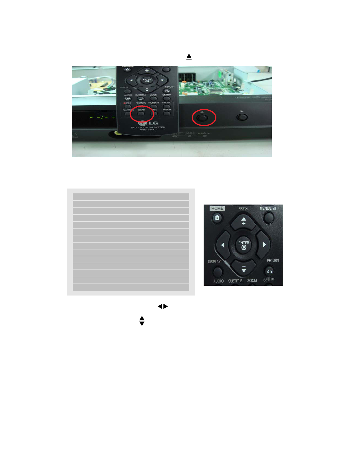
1. Please the CLEAR button on the remocon together with OPEN the Front Panel about 6 sec.
The picture on OSD will be bellow ;
Model :
Disc Read Time
DVD 018 Sec OK
CD 021 Sec NG
OP1 : 00 00000000 M : 10.013
OP2 : 00 00000000 E : FF(OR)
OP3 : 00 00000000
OP4 : 00 00000000
OP5 : 00 00000000
OP6 : 00 00000000
OP7 : 00 00000000 Write : OK
OP8 : 00 00000000 E x i t : MP
OP9 : 00 00000000 Move : < >
OPA : 00 00000000 E d i t :
2. To MOVE from OP! to another option. Please button on the remote control.
3. To CHANGE the Option Code. Please button on the remote control.
4. To APPLY the Option Code. After change the option press ENTER button on remote control.
5. To INITIALIZE the system. Press CLEAR button on the remotecontrol together with OPEN on the Front panel
about 2sec.
6. To exit from the Option Code menu without Initialize the system.
Just turn off the power and turn on again.
LGE Internal Use Only
1-6
Copyright © 2008 LG Electronics. Inc. All right reserved.
Only for training and service purposes
Page 8
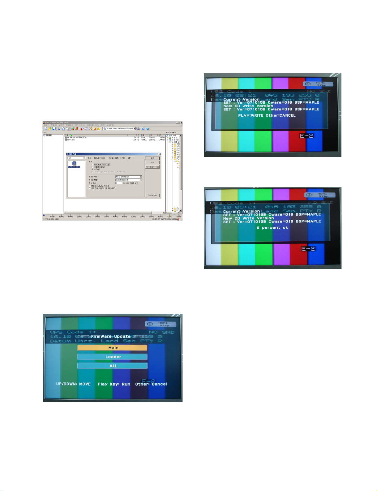
UPGRADE THE MAIN & LOADER PROGRAM
1. MAKING UPGRADE DISC
1) Do Physical format as ISO9660 or JOLIET file
system
2) Don’t care about the CD Volume label
3) Write RH300 B_E & LOADER file on Root
4) Write I_O file on Root
Note) You can’t write steps 3 and 4 on the same disc.
Use the different disc to write another step.
* OPTIONAL PARTS
1) B_E
LG_RH300_UPDATE_PAL.ROM
2) LOADER
DvdS617.rs6, Yas617.din
3) I_O
io_micom_update.hex
2. UPGRADE FLASH (MAIN & LOADER) and I_O
1) Put Upgrde DISC on the Set
2) After Disc Reading, You can see below screen
3) Press ENTER (or OK) KEY.
You can see both current and upgrade version.
4) Press PLAY KEY.
Start upgrading.
5) After upgrading, Automatically open tray.
Eject the Disc.
Reboot the Set
6) Put I_O update disc and repeat 1) ~ 5)
* OPTIONAL PARTS
1) MAIN
ONLY B_E UPGRADE
2) LOADER
ONLY LOADER UPGRADE
3) ALL
B_E & LOADER UPGRADE
Copyright © 2008 LG Electronics. Inc. All right reserved.
Only for training and service purposes
1-7
LGE Internal Use Only
Page 9

SPECIFICATIONS
• GENERAL
Power requirements AC 200-240V, 50/60 Hz
Power consumption 30W
Dimensions (approx.) 430 X 49 X 275mm (w x h x d) without foot
Net weight (approx.) 4kg
Operating temperature 5°C to 35°C
Operating humidity 5% to 65%
Television system PAL I, B/G, I/I, SECAM D/K, K1 color system
Recording format PAL
• RECORDING
Recording format DVD Video Recording, DVD-VIDEO
Recordable media HDD (320GB), DVD-RW, DVD-R, DVD+RW,
DVD+R, DVD+R (Double Layer), DVD-RAM
Recordable time DVD (4.7GB): Approx. 1 hour (XP mode),
2 hours (SP mode), 4 hours (LP mode),
6 hours (EP mode), 14 hours (MLP mode)
DVD+R DL (8.5GB): Approx. 3hours (XP mode),
3.8 hours (SP mode), 7.3 hours (LP mode),
9.1 hours (EP mode), 21 hours (MLP mode)
HDD (320GB, MPEG2 Recording):
Approx. 85 hours (XP mode), 165 hours (SP mode),
323 hours (LP mode), 456 hours (EP mode),
935 hours (MLP mode)
Video recording format
Sampling frequency 27MHz
Compression format MPEG2 (VBR supported)
Audio recording format
Sampling frequency 48kHz
Compression format Dolby Digital
• PLAYBACK
Frequency response DVD (PCM 48kHz): 8Hz to 22kHz,
CD: 8Hz to 20kHz
DVD (PCM 96kHz): 8Hz to 44kHz
Signal-to-noise ratio More than 90dB (AUDIO OUT connector)
Harmonic distortion Less than 0.02% (AUDIO OUT connector)
• INPUTS
Dynamic range More than 95dB (AUDIO OUT connector)
ANTENNA IN Antenna input, 75ohms
VIDEO IN 1.0 Vp-p 75ohms, sync negative, RCA jack x 1 / SCART x 2
AUDIO IN 2.0 Vrms more than 47kohms, RCA jack (L, R) x 1 / SCART x 2
DV IN 4 pin (IEEE 1394 standard)
USB IN 4 pin (USB 1.1 standard)
• OUTPUTS
VIDEO OUT 1Vp-p 75Ω, sync negative, SCART x 2
S-VIDEO OUT (Y) 1.0V (p-p), 75Ω, sync negative,
Mini DIN 4-pin x 1(C) 0.3V (p-p) 75Ω
COMPONENT VIDEO OUT (Y) 1.0V (p-p), 75Ω, sync negative,
RCA jack x 1, (PB)/(PR) 0.7V (p-p), 75Ω, RCA jack x 2
HDMI video/audio output 19 pin (HDMI standard, Type A)
Audio output (digital audio) 0.5V (p-p), 75Ω, RCA jack x 1
Audio output (optical audio) 3V (p-p), Optical connector x 1
Audio output (analog audio) 2Vrms (1kHz, 0dB), 600Ω, RCA jack (L, R) x 2 / SCART x 2
LGE Internal Use Only
1-8
Copyright © 2008 LG Electronics. Inc. All right reserved.
Only for training and service purposes
Page 10

SECTION 2
CABINET & MAIN CHASSIS
CONTENTS
EXPLODED VIEWS .....................................................................................................................................2-2
1. CABINET AND MAIN FRAME SECTION ..................................................................................................2-2
2. DECK MECHANISM SECTION (RS-06A).................................................................................................2-3
3. PACKING ACCESSORY SECTION...........................................................................................................2-4
Copyright © 2008 LG Electronics. Inc. All right reserved.
Only for training and service purposes
2-1
LGE Internal Use Only
Page 11
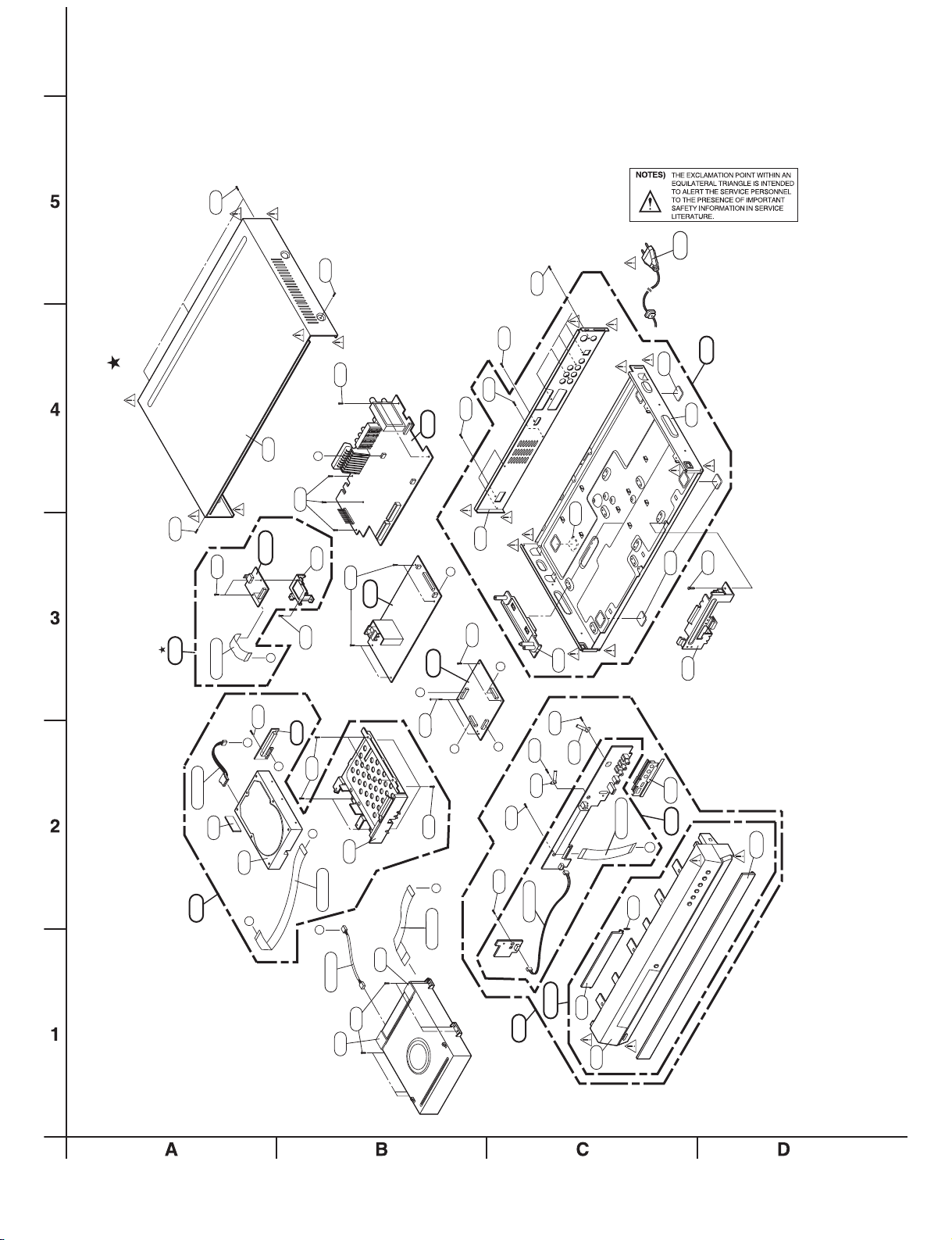
EXPLODED VIEWS
1. CABINET AND MAIN FRAME SECTION
462
462
OPTIONAL PARTS
8
250
46
A52
G
465
5
46
300
465
70
4
A44
261
0
26
462
A54
468
CABLE7
CABLE10
261
A26
104
A54A
HDMI
468
BOARD
253
468
I/O BOARD
261
320
A
8
1
46
26
A47
SMPS
468
C
C
8
46
G
E
A53
F
468
F
101
ABLE11
C
A
CABLE6
8
46
261
471
261
410
46
A
ABLE5
C
468
452
275
CABLE1
264
452
A43A
275
285
TIMER
CABLE2
286
73
2
4
27
50
A
D
281
E
MAIN
BOARD
D
B
452
B
452
KEY
A43
280
LGE Internal Use Only
2-2
Copyright © 2008 LG Electronics. Inc. All right reserved.
Only for training and service purposes
Page 12
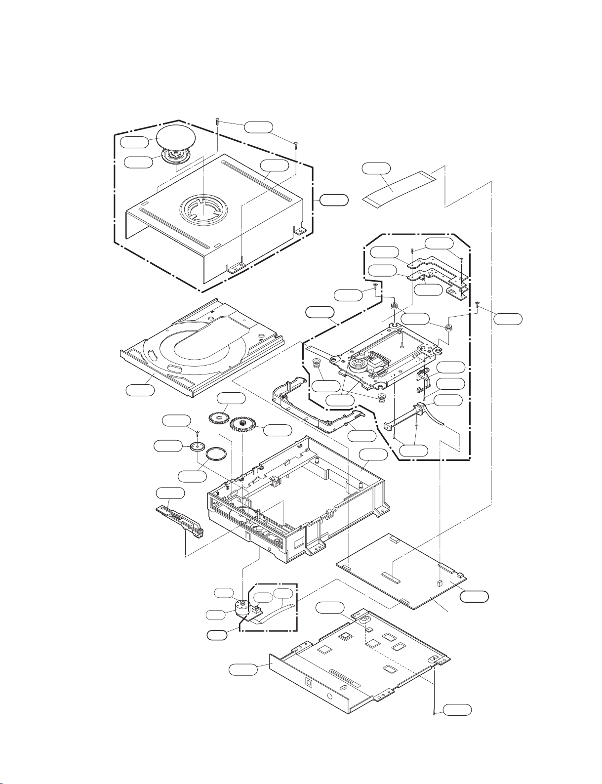
2. DECK MECHANISM SECTION (RS-06A)
1431
1001
RS-06A(DR-11H)
1003
1026
1433
1016
1017
1002
1013
A001
A006
1041
1437
1432
1011
1020
1030
1033
1032
1025
1432
1434
1034
1437
1038
1432
1036
1015
1012
1019
1018
A
0
0
5
1047
Copyright © 2008 LG Electronics. Inc. All right reserved.
Only for training and service purposes
1043
1045
2-3
1046
A46A
M
a
in
C
.
B
.
A
1439
LGE Internal Use Only
Page 13
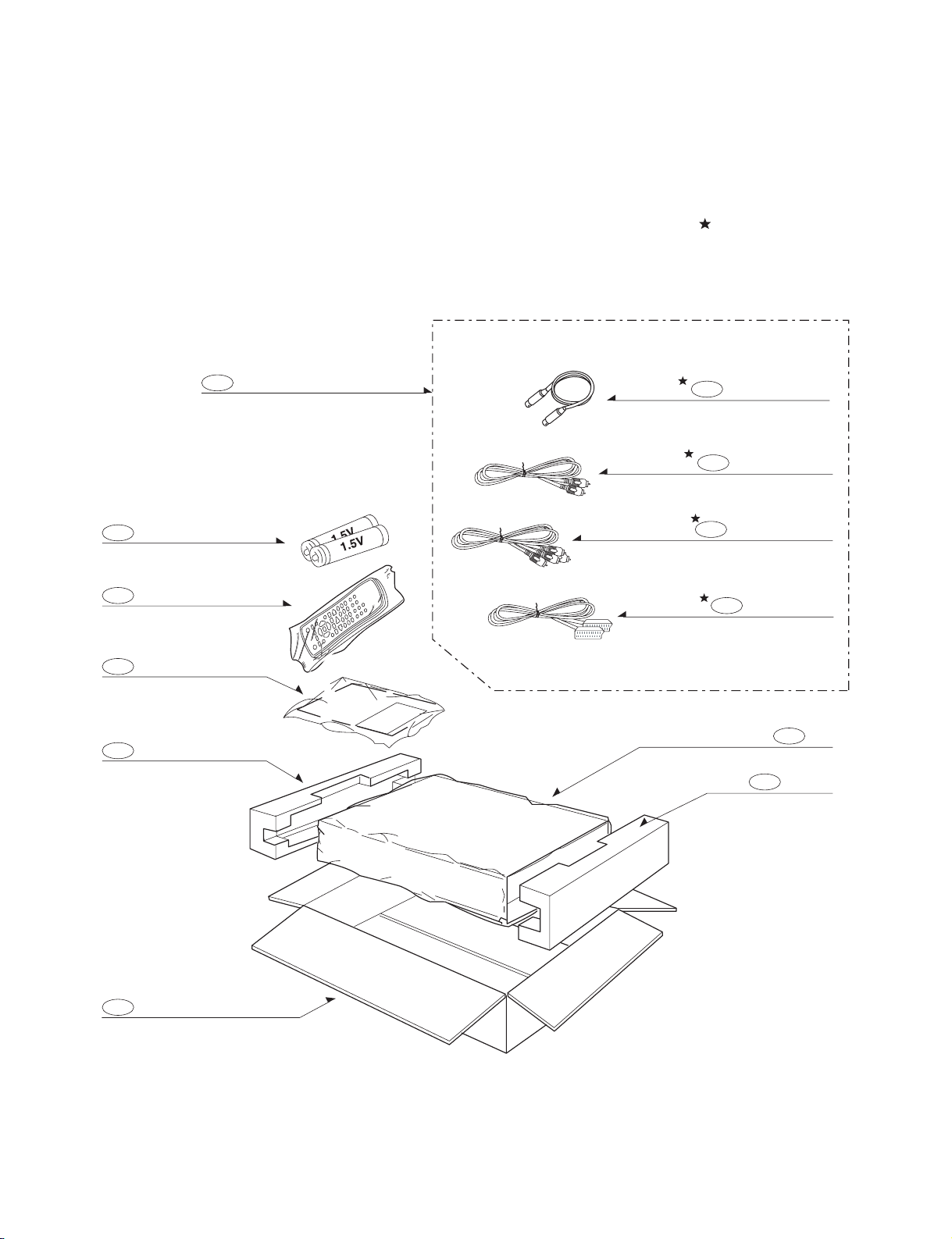
3. PACKING ACCESSORY SECTION
OPTIONAL PARTS
810 Accessory Assembly
808 Battery
900 Remote Control
Instruction Ass'y
801
803 Packing
806 RCA Plug(Black)
Plug Ass'y 1way
811
812
Plug Ass'y 2way
821 SCART Cable
804 Bag
803 Packing
Box
802
LGE Internal Use Only
2-4
Copyright © 2008 LG Electronics. Inc. All right reserved.
Only for training and service purposes
Page 14

SECTION 3
ELECTRICAL
CONTENTS
ELECTRICAL TROUBLESHOOTING GUIDE
1. POWER SUPPLY ON SMPS BOARD .............3-2
2. POWER SUPPLY ON I/O BOARD ...................3-4
3. SYSTEM CIRCUIT PART ..................................3-9
4. DISC NOT RECOGNIZED.................................3-9
5.
WHEN PLAYING DISC, NO AUDIO OUTPUT
6. NO OPTICAL/DIGITAL OUTPUT ....................3-11
7. NO TUNER AUDIO OUTPUT .........................3-12
8. NO EXTERNAL AUDIO INPUT .......................3-13
9. NO RGB/COMPONENT VIDEO SIGNAL
WHEN PLAY DISC ...........................................3-14
10. NO COMPOSITE/S-VIDEO SIGNAL
WHEN PLAY DISC............................................3-15
11. NO TV, EXTERNAL INPUT VIDEO
SIGNAL..............................................................3-16
12. NO DV (IEEE1394)
INPUT (VIDEO/AUDIO) SIGNAL.....................3-17
...........3-2
..........3-10
WAVEFORMS..........................................................3-18
1. SMPS BLOCK ..................................................3-18
2. SYSTEM BLOCK .............................................3-20
3. VIDEO BLOCK (COLOR BAR INPUT)...........3-23
4. AUDIO BLOCK (1kHz SINEWAVE INPUT)....3-24
5. SERIAL INTERFACE BLOCK
(BETWEEN MAIN AND I/O)............................3-25
6. TUNER BLOCK ................................................3-26
7. HDMI BLOCK ...................................................3-27
WIRING CONNECTION DIAGRAM...............3-28
1. WIRING CONNECTION DIAGRAM 1 ............3-28
2. WIRING CONNECTION DIAGRAM 2 ............3-29
3. WIRING CONNECTION DIAGRAM 3 ............3-30
BLOCK DIAGRAMS.............................................3-31
1. VERALL BLOCK DIAGRAM............................3-31
2. SMPS BLOCK DIAGRAM ...............................3-32
3. POWER MAIN BLOCK DIAGRAM .................3-33
4. POWER I/O BLOCK DIAGRAM......................3-34
5. A/V BLOCK DIAGRAM ....................................3-35
6. AUDIO OUT BLOCK DIAGRAM .....................3-36
7. HDMI BLOCK DIAGRAM ................................3-37
CIRCUIT DIAGRAMS...........................................3-39
1. SMPS 1 CIRCUIT DIAGRAM..........................3-39
2. SMPS 2 CIRCUIT DIAGRAM..........................3-41
3. MPEG CIRCUIT DIAGRAM.............................3-43
4. FLASH/DDR/DV CIRCUIT DIAGRAM............3-45
5. ATAPI, HDMI & USB CIRCUIT DIAGRAM.....3-47
6. I/O, µ-COM CIRCUIT DIAGRAM ....................3-49
7. DECODER & MIC CIRCUIT DIAGRAM.........3-51
8. SCART/RCA CIRCUIT DIAGRAM..................3-53
9. HDMI CIRCUIT DIAGRAM ..............................3-55
10. TIMER CIRCUIT DIAGRAM
11. KEY CIRCUIT DIAGRAM (8 & 9 TOOLS) ......3-59
(8 & 9 TOOLS)
...3-57
• CIRCUIT VOLTAGE CHART ....................3-61
PRINTED CIRCUIT BOARD DIAGRAMS...3-65
1. MAIN P.C.BOARD ............................................3-65
2. I/O P.C.BOARD.................................................3-67
3. POWER P.C.BOARD .......................................3-71
4. TIMER & KEY P.C.BOARD..............................3-73
5. HDMI P.C.BOARD ............................................3-75
Copyright © 2008 LG Electronics. Inc. All right reserved.
Only for training and service purposes
3-1
LGE Internal Use Only
Page 15
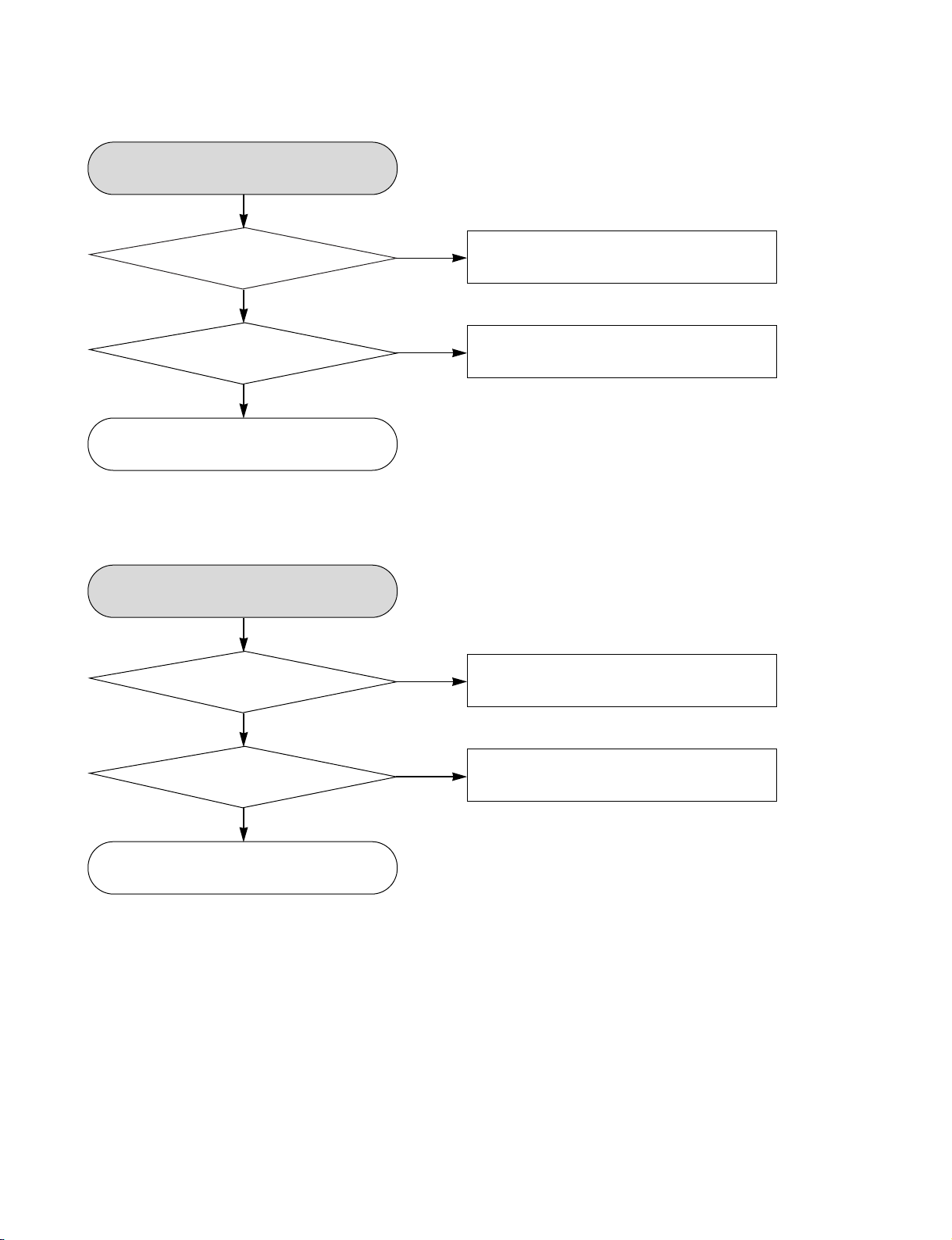
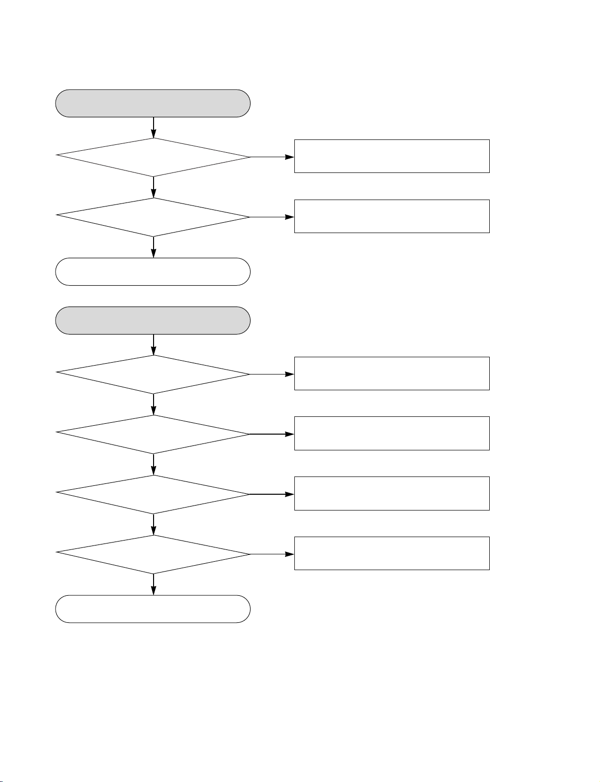
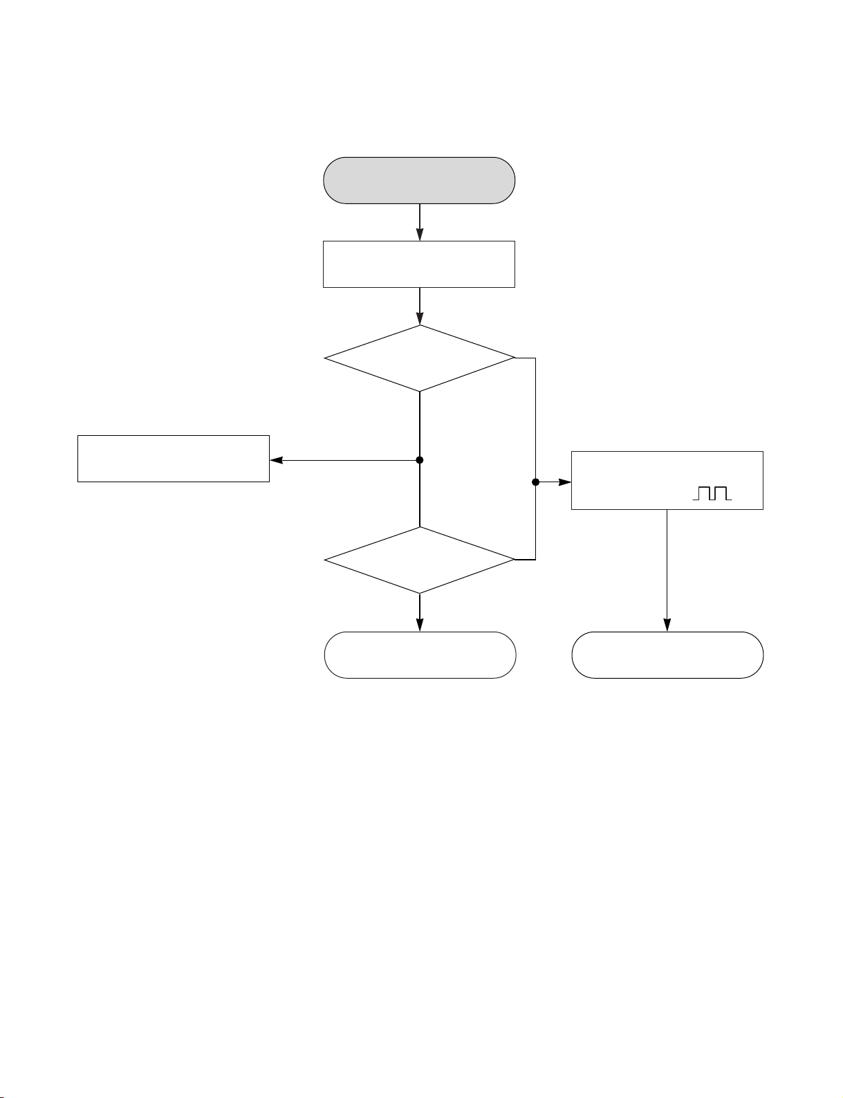
ELECTRICAL TROUBLESHOOTING GUIDE
1. POWER SUPPLY ON SMPS BOARD
No 5.3VA
YES
Is the F101 normal? Replace the F101 (Use the same fuse)
YES
Is the BD101 normal? Replace the BD101
YES
Is the TH01 normal? Replace the TH01
YES
NO
NO
NO
Is the Vcc
(10V - 17V) supplied to
NO
Is the D102 normal?
IC101 Pin 6?
NO
YES
Is the D128 normal? Replace the D128
YES
Is there about 2.5V at the
NO
NO
Check or replace the D102
Replace the IC103
IC103 Pin 1?
YES
Is the D121 normal? Replace the D121
YES
Is the D122 normal? Replace the D122
YES
Is the D125 normal? Replace the D125
YES
Is the D124 normal? Replace the D124
NO
NO
NO
NO
Is the D127 normal?
Is the D126 normal? Replace the D126
Power line of I/O PCB is short
LGE Internal Use Only
YES
YES
YES
NO
NO
3-2
Replace the D127
Copyright © 2008 LG Electronics. Inc. All right reserved.
Only for training and service purposes
Page 16
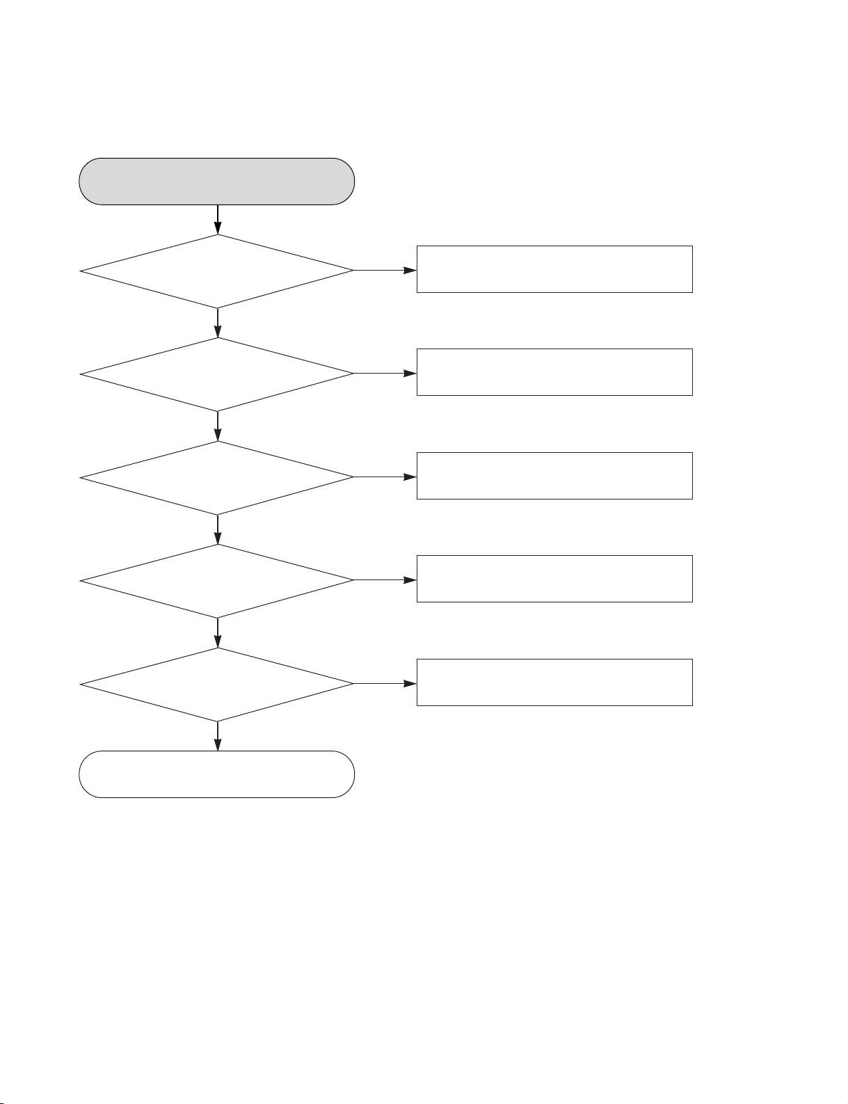
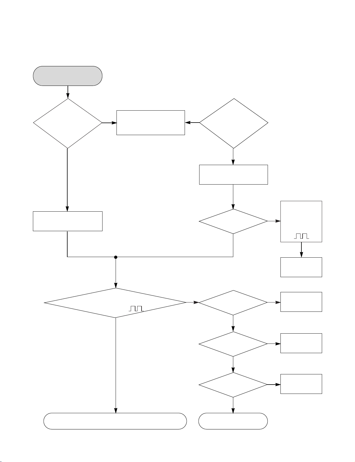
No 5V for HDD & DVD drive
YES
Is there about 5.5V at
the IC156 Pin 1?
YES
Is there about 4V ~ 5V at
the IC156 Pin 4?
YES
Check the IC156 and replace
No 12V for HDD & DVD drive
YES
Is there about 13.5V at
the IC155 Pin 1?
NO
NO
NO
Check D125 and replace
Check the “PWR CTL‘H’”
signal from µ-COM
Check D124 and replace
YES
Is there about 4V ~ 5V at
the IC155 Pin 4?
YES
Check the IC155 and replace
Copyright © 2008 LG Electronics. Inc. All right reserved.
Only for training and service purposes
NO
3-3
Check the “PWR CTL ‘H’”
signal from µ-COM
LGE Internal Use Only
Page 17
2. POWER SUPPLY ON I/O BOARD
No 12VT
YES
Is the Vcc (14V) supplied to
Q164 collector?
YES
Is there about 12.5V at
ZD151 & Q164 base?
YES
Is the Vcc (33V) supplied
to Q162 emiter?
YES
Is there about 0V at
Q162 base?
YES
NO
NO
NO
NO
Check D124 on SMPS
board and replace
Check Q164 and replace
Check D126 on SMPS
board and replace
Check Q162 and replace
Is there about 5V at R170
and 0.7V at Q156 base?
Check Q156 and replace
LGE Internal Use Only
YES
NO
3-4
Check the “TIMER_H”
signal from µ-COM
Copyright © 2008 LG Electronics. Inc. All right reserved.
Only for training and service purposes
Page 18
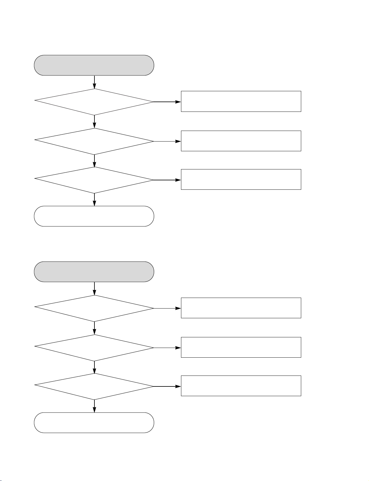
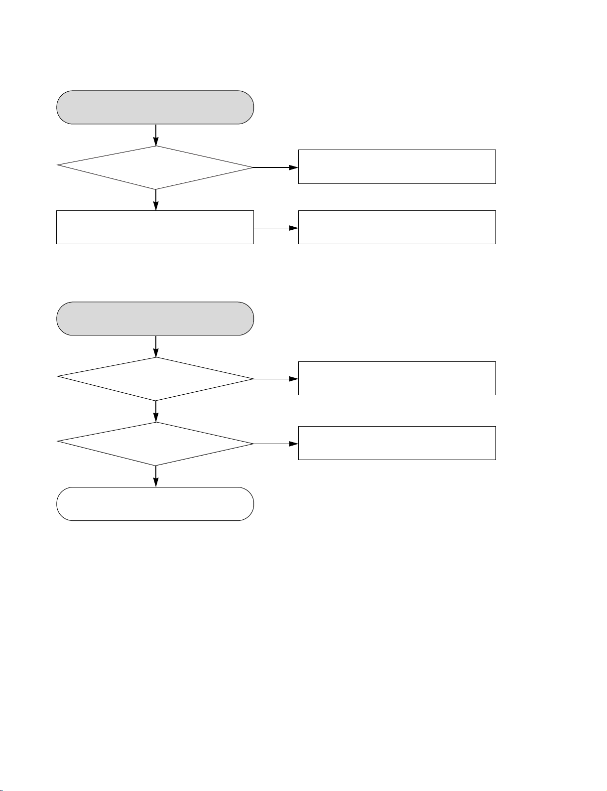
No 5VT
YES
Is the Vcc (5.3V)
supplied to Q155 emiter?
YES
Is there about 0V
at D152 and
Q152 vollector?
YES
Is there about 5V
at R180 and 0.7V
at Q152 base?
YES
Check Q152 and replace
No 33VT
NO
NO
NO
Check 5.3VA on SMPS board
Check Q155 and replace
Check the “TIMER H”
signal from µ-COM
YES
Is the Vcc (33V)
supplied to Q161 emiter?
YES
Is there about 0V at
Q152 collector?
YES
Is there about 5V
at R180 and 0.7V
at Q152 base?
YES
Check Q152 and replace
Copyright © 2008 LG Electronics. Inc. All right reserved.
Only for training and service purposes
NO
NO
NO
3-5
Check D126 on SMPS
board and replace
Check Q161 and replace
Check the “TIMER H”
signal from µ-COM
LGE Internal Use Only
Page 19
No 5.0VD
YES
Is there about 5.3V at
the IC153 Pin 1?
YES
Is there about 4V ~ 5V at
the IC153 Pin 4?
YES
Check the IC153 and replace
No 2.5V
YES
Is there about 3V ~ 3.8V
at the IC151 Pin 1?
YES
Is there about 4V ~ 5V at
the IC151 Pin 4?
NO
NO
NO
NO
Check 5.3VA on SMPS board
Check the “PWR CTL H”
signal from µ-COM
Check D154 and
D127 on SMPS board
Check the “PWR CTL H”
signal from µ-COM
Check the IC151 and replace
Is there about 3.8V at
the IC152 Pin 1?
Is there about 4V ~ 5V at
the IC152 Pin 4?
Check the IC152 and replace
LGE Internal Use Only
YES
No 3.3V
YES
YES
YES
NO
NO
3-6
Check D127 on SMPS
board and replace
Check the “PWR CTL H”
signal from µ-COM
Copyright © 2008 LG Electronics. Inc. All right reserved.
Only for training and service purposes
Page 20
No SW_5.3VA
YES
Is the Vcc (5.3V)
supplied to Q158 emiter?
YES
Is there about 0V
at R179 and R156?
YES
Check Q158 and replace
No SW_FD(+)
YES
Is the Vcc (FD+) supplied
to Q163 collector?
YES
Is there about 5.3V at
R184 and Q153 collector?
NO
NO
NO
NO
Check 5.3VA on SMPS board
Check the “STANBY H”
signal from µ-COM
Check D121 on SMPS
board and replace
Check Q163 and replace
YES
Is the VCC (5.3V)
supplied to Q153 emiter?
YES
Is there about 0V
at Q153 base?
YES
Check Q153 and replace
Copyright © 2008 LG Electronics. Inc. All right reserved.
Only for training and service purposes
NO
NO
3-7
Check 5.3VA on SMPS board
Check the “STANBY H”
signal from µ-COM
LGE Internal Use Only
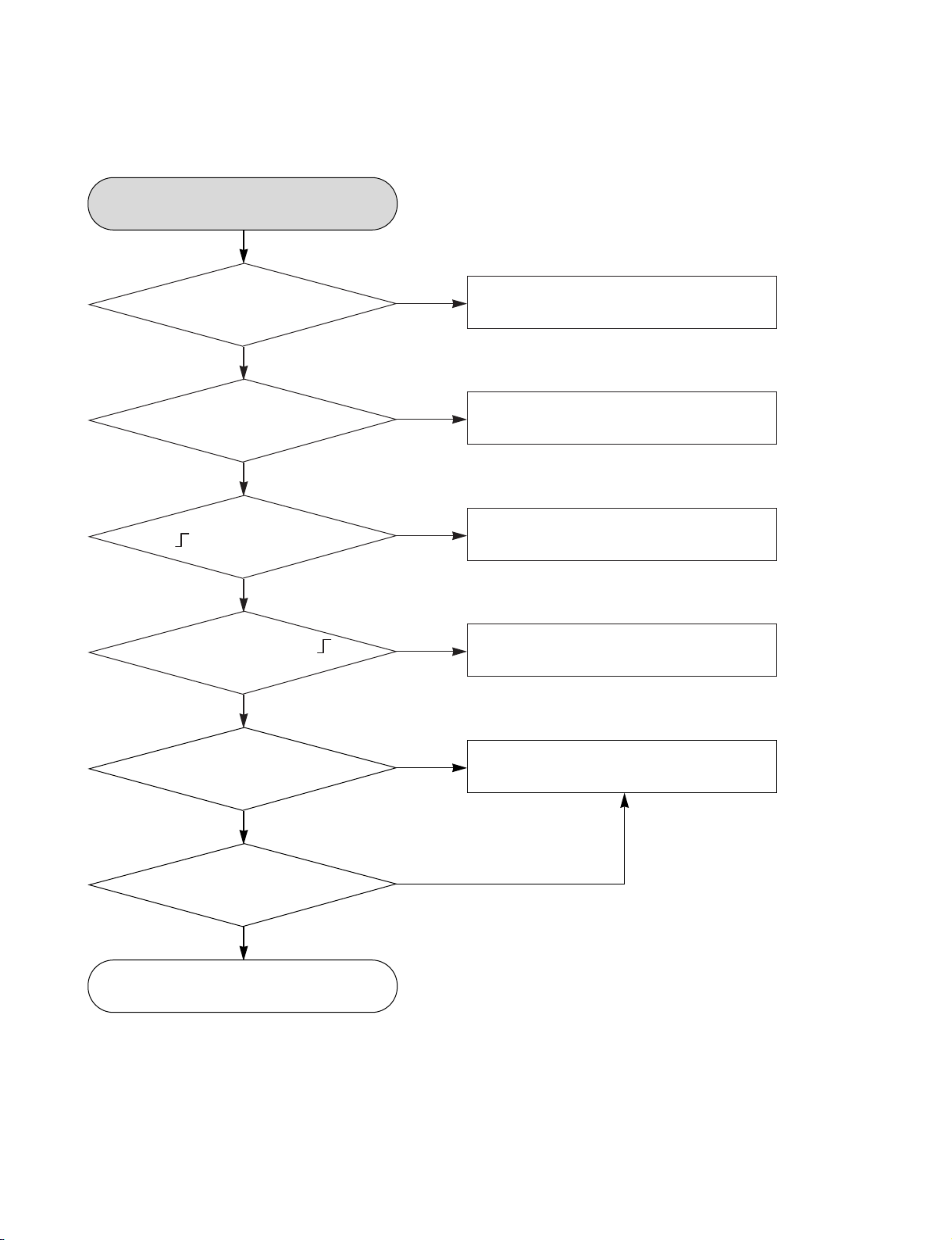
Page 21
No 1.8V
YES
Is the Vcc (3.3V)
supplied to Pin 3 IC155?
YES
There is 1,8V at IC155 Pin 2, 4
No 1.25V
YES
Is there about 5.3V at
the IC154 Pin 2?
YES
Is there about 4V ~ 5V at
the IC154 Pin 5?
NO
NO
NO
NO
Check 3.3V power supply
IC155 defect
Check 5.3VA on SMPS board
Check the “PWR CTL H”
signal from µ-COM
Check the IC154 and replace
LGE Internal Use Only
YES
3-8
Copyright © 2008 LG Electronics. Inc. All right reserved.
Only for training and service purposes
Page 22
3. SYSTEM CIRCUIT PART
“Please wait” displayed
continue at power on
YES
IC1306 Pin 5 : ?
(/HOST-RESET)
YES
X1101 : Clock oscillated?
(13.5MHz)
YES
AR1105 Pin 3 : ?
IC1201 Pin 32 : ?
YES
R1173, R1174 : ?
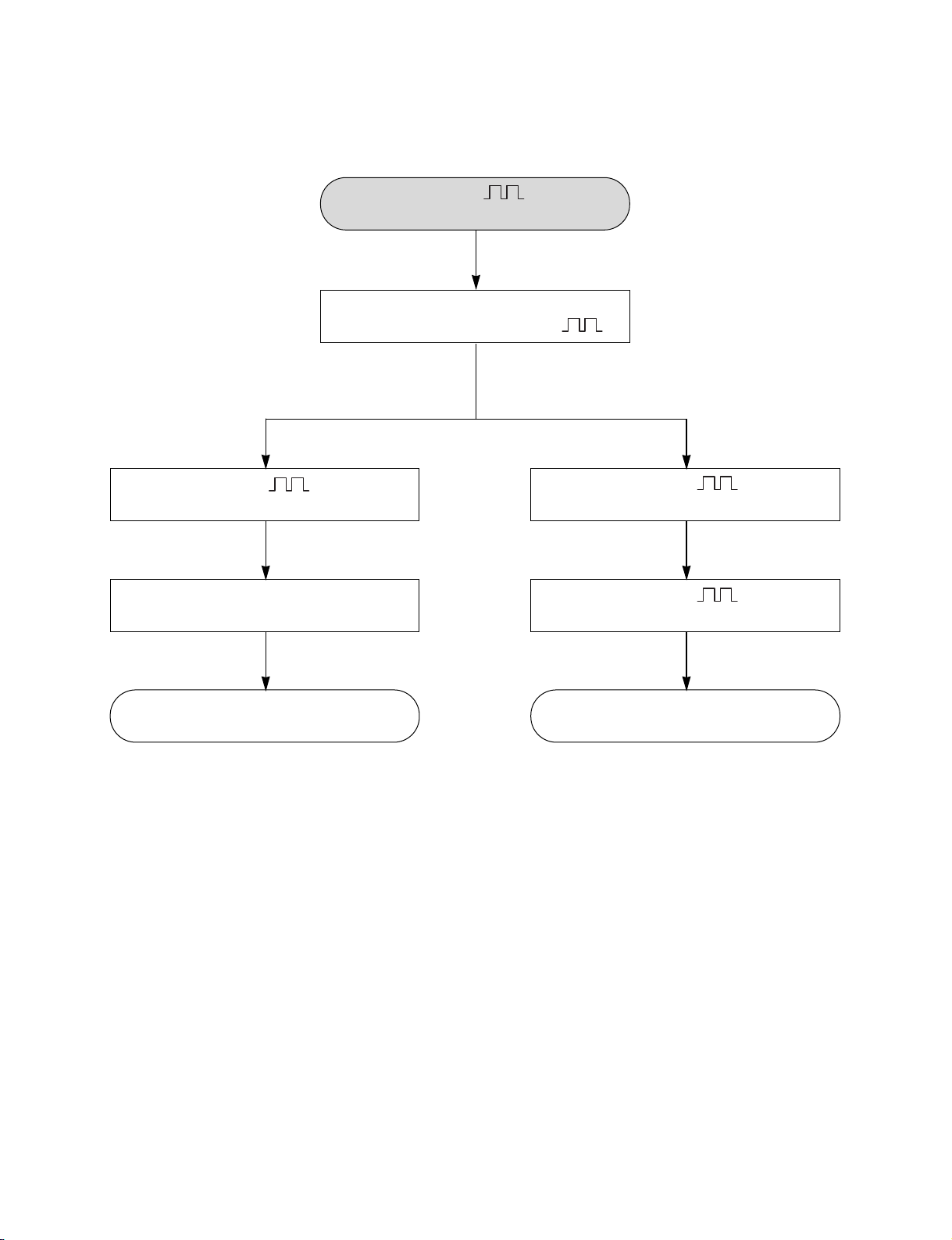
4. DISC NOT RECOGNIZED
NO
NO
NO
NO
Check PVM02 Pin 25 IC 701 Pin 19
Replace X1101
Check IC1201 (Flash memory) & IC1101
IC1101 defect
DISC not recognized
Check driver power?
5V, 12V
YES
Check ATAPI connector
YES
Check loader
Copyright © 2008 LG Electronics. Inc. All right reserved.
Only for training and service purposes
NO
NO
3-9
Check SMPS
Change MEDIA TEST
LGE Internal Use Only
Page 23
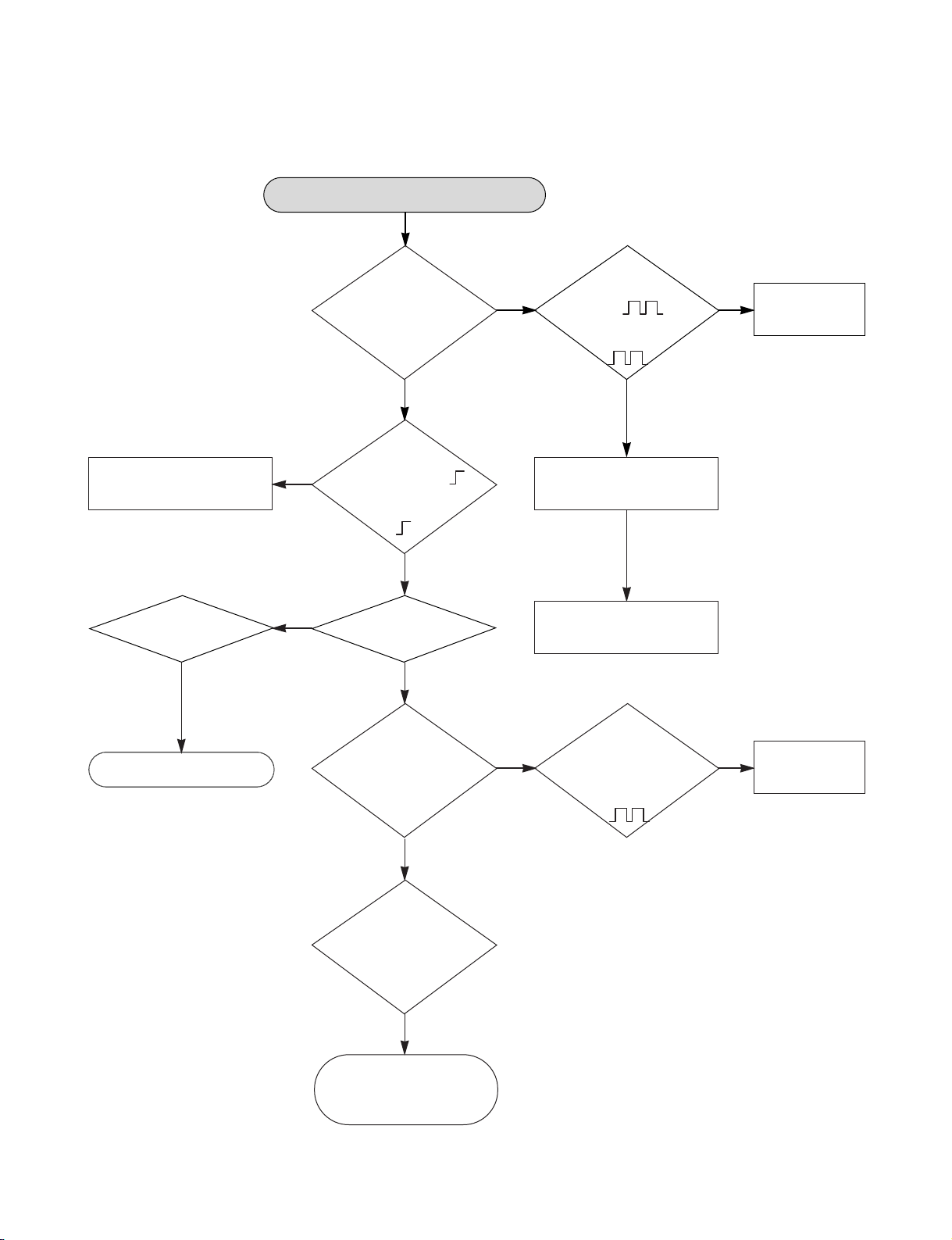
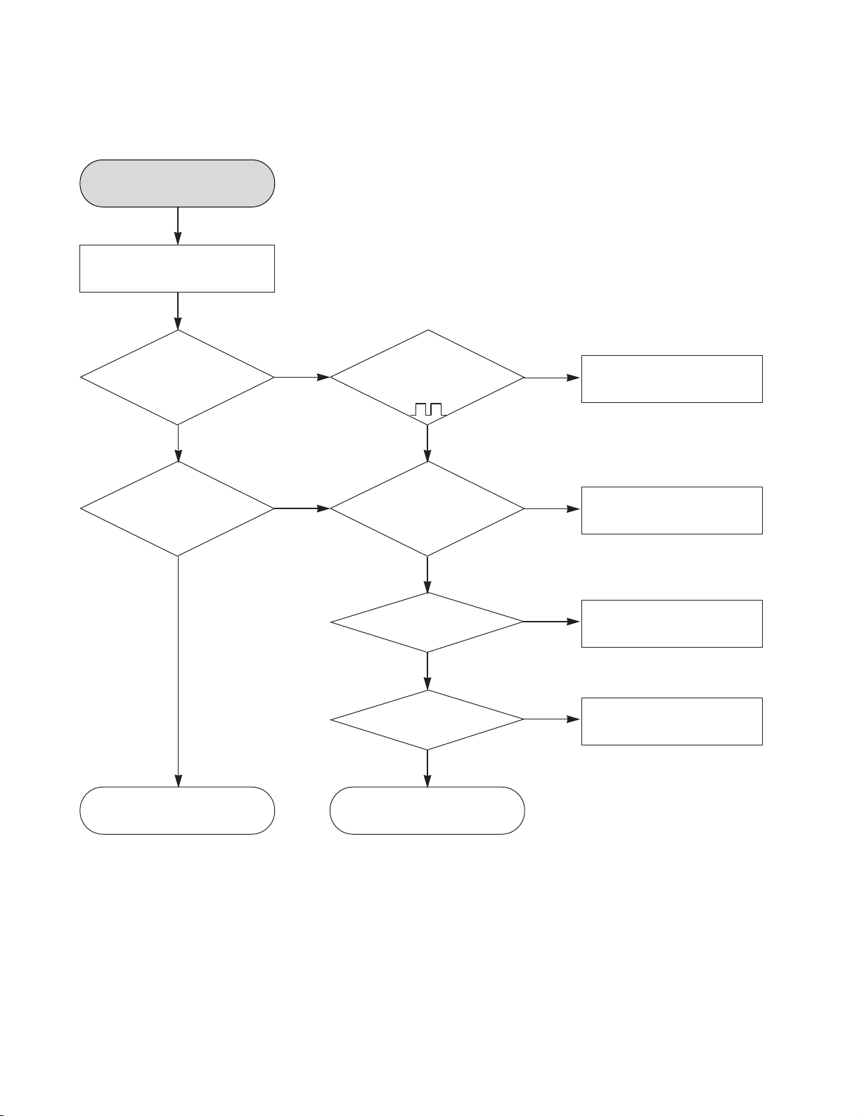
5. WHEN PLAYING DISC, NO AUDIO OUTPUT
When playing DISC, no Audio output
IC904 Pin 14, 15 :
Is there a signal?
YES
NO NO
Check
IC904 Pin 5, 6,
7, 8 : .
Pin 3, 4 (Host CLK
& DATA) :
YES
IC1101 defect
Check
Q808, Q809, Q810, Q801
Check
IC902 Pin 8
(12VT)
YES
Replace IC902
NO
IC904 Pin 1, 16
(Z_MUTE R/L) : .
IC701 Pin 24
(A_MUTE_L) :
NO
IC902 Pin 1, 7 :
Is there a signal
IC801 Pin 34, 35,
37, 38 : Is there
a signal?
YES
YES
YES
Check
IC904 Pin 11 (5VD)
YES
Replace IC904
Check
NO NO
IC801 Pin 14
(12V) Pin 30 (5, 3V)
Pin31, 32
(SCL, SDA) :
Replace
IC801
LGE Internal Use Only
L804, L808,
L820, L821 :
Is there a signal?
YES
Check
cable connections &
TV audio mute.
3-10
Copyright © 2008 LG Electronics. Inc. All right reserved.
Only for training and service purposes
Page 24
6. NO OPTICAL/DIGITAL OUTPUT
R1107 : .
Is there a signal?
PVM02 Pin 1 (SPDIF_OUT) : .
YES
Check
YES
R832 : .
Is there a signal?
YES YES
Check JK803 Pin 2 (5V)
YES YES
Check JK803 &
optical cable connection
C839 : .
Is there a signal?
BD803 : .
Is there a signal?
Check JK802 &
RCA cable connection
Copyright © 2008 LG Electronics. Inc. All right reserved.
Only for training and service purposes
3-11
LGE Internal Use Only
Page 25
7. NO TUNER AUDIO OUTPUT
TU701 Pin 16 (SIF) :
Is there a signal?
YES
IC901 Pin 106, 107
Is there a signal?
YES
IC801 Pin 40, 41 :
Is there a signal?
NO
Pin 30 (5, 3V) Pin 31, 32
Check
IC801 Pin 14 (12V)
(SCL, SDA) :
NO
Replace IC801
YES
IC901 Pin 98,
99, 100, 95 (Ain_D0,
AIN_SCLK, AIN_FSYNC,
AIN_MCLK) : Is there
a signal?
YES
When playing DISC,
no audio output
NO
YES
Check Pin 51/
RST_SAA7138
YES
X901 (24.576MHz)
oscillated?
YES
R906, R909
(SCL/SDA)
YES
IC901 defect
NO
NO
NO
Check IC1302
reset circuit
Change X901
Check IC901 power
3.3V & 1.8V
LGE Internal Use Only
3-12
Copyright © 2008 LG Electronics. Inc. All right reserved.
Only for training and service purposes
Page 26
8. NO EXTERNAL AUDIO INPUT
< AV3 > < AV1/AV2>
C9F3, C9F4 :
Is there a signal?
YES
NO
IC801 pin 2, 3, 5, 6 :
Check
cable connections
& input signal.
IC803 Pin 40, 41 :
AIN_SCLK, AIN_FSYNC,
Is there a signal?
YES
Is there a signal?
YES
IC901
Pin 98, 99,100,
95 (Ain_D0,
AIN_MCLK) :
Is there
a signal?
IC801 Pin 14 (12V)
NO
Pin 30 (5, 3V)
Pin 31, 32
(SCL, SDA) : .
NO
Check Pin 51/
RST_SAA7138
Check
NO
NO
Replace
IC801
Check
IC1302 reset
circuit
YES
When playing DISC,
no audio output
YES
X901
(24.576MHz)
oscillated?
YES
R906, R909
(SCL/SDA)
YES
IC901 defect
NO
NO
Change X901
Check
IC901 power
3.3V & 1.8V
Copyright © 2008 LG Electronics. Inc. All right reserved.
Only for training and service purposes
3-13
LGE Internal Use Only
Page 27
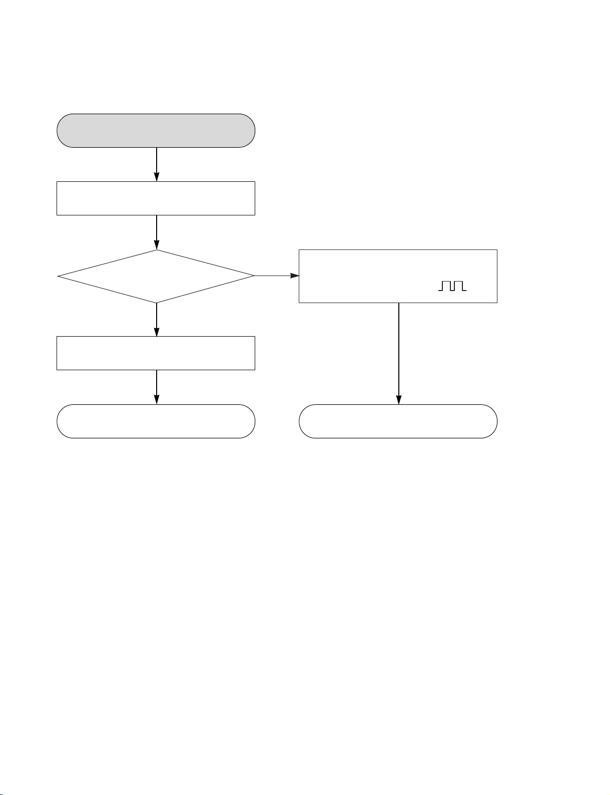
9. NO RGB/COMPONENT VIDEO SIGNAL WHEN PLAY DISC
R1160, R1161, R1162 :
Is there a signal?
YES
PVM01 Pin 13, 14, 16 :
Is there a signal?
YES
IC801 Pin 24, 25, 26 :
Is there a signal ?
YES
NO
Check IC801 Pin 14 (12V)
Pin 30 (5, 3V)
Pin 31, 32 (SCL, SDA) : .
Check condition
RGB_Sel_Out & Ypbpr_Mute_L
YES
Check cable connection Replace IC801
YES
LGE Internal Use Only
3-14
Copyright © 2008 LG Electronics. Inc. All right reserved.
Only for training and service purposes
Page 28
10. NO COMPOSITE/S-VIDEO SIGNAL WHEN PLAY DISC
R1157, 1158, 1159 :
Is there a signal?
YES
PVM01 Pin 18, 19, 20 :
Is there a signal?
YES
IC801 Pin 27, 29, :
Is there a signal?
YES
Check S-VIDEO
cable connection
(S-VIDEO)
(SCART)
IC801 Pin 36, 39, :
Is there a signal?
YES
Check SCART
cable connection
NO
Check IC801 Pin 14 (12V)
Pin 30 (5, 3V) Pin 31, 32
(SCL, SDA) : .
YES
Replace IC801
Copyright © 2008 LG Electronics. Inc. All right reserved.
Only for training and service purposes
3-15
LGE Internal Use Only
Page 29
11. NO TV, EXTERNAL INPUT VIDEO SIGNAL
No TV, external input
video signal
No video
signal of external
input AV3
(Front
RCA input)
YES
R905 :
Is there a signal?
NO
Check
cable connection &
input signal
When cable
NO
connecting tuner
and rear SCART 1, 2
no TV video signal
(AV1/2)
C843, C863, C864 :
Is there a signal?
IC 801 Pin 42 :
Is there a signal?
YES
YES
YES
IC801 Pin 14
NO
(12V) Pin 30
(5, 3V) Pin 31,
32 (SCL, SDA)
Check
: .
YES
Replace
IC801
Check no RGB / Component / Composite /
LGE Internal Use Only
IC901 Pin (56, 57, 58,
61,62, 63, 64, 65) VIND2-VIND9
is there a signal .
YES
S-VIDEO signal when play DISC
3-16
Check Pin 51
/RST_SAA7138
YES
X901
(24.576MHz)
oscillated?
YES
R906,
R909 (SCL/SDA), L917
(VinCLK)
YES
NONO
NO
NO
Check
IC1302 reset
circuit
Change
X901
Check
IC901 power
3.3V & 1.8V
IC901 defect
Copyright © 2008 LG Electronics. Inc. All right reserved.
Only for training and service purposes
Page 30
12. NO DV (IEEE1394) INPUT (VIDEO/AUDIO) SIGNAL
Check DV_Jack connection
YES
DV-mode switching?
YES
IC1401 power 3.3V
YES
IC1401 Pin 37 : “High”
& X401 (24.576MHz)
oscillated ?
YES
IC1401 pin 15 : “High” .
Is there a signal?
YES
NO
NO
NO
NO
Change to DV-mode.
using remote control
Check power 3.3V on I/O board
Check IC1302 reset circuit
Check DV cable
IC1401
Pin 1, 27, 28, 29, 30 :
Is there a signal?
YES
IC1401 Pin 2, 3 :
Is there a signal?
NO
IC101 defect
Copyright © 2008 LG Electronics. Inc. All right reserved.
Only for training and service purposes
NO
YES
3-17
Replace IC1401
LGE Internal Use Only
Page 31

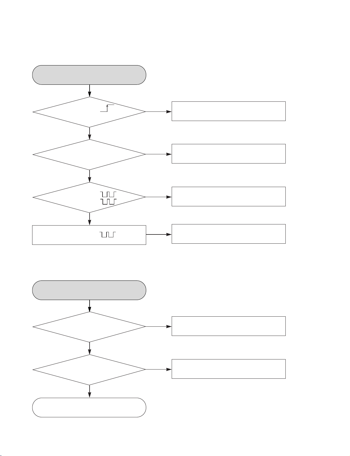
1. SMPS BLOCK
1
< Switching waveform of IC101,
when power is on >
WAVEFORMS
1
2
< Both ends waveform of D128,
when power is on (feedback 5.3VA) >
2
LGE Internal Use Only
3-18
Copyright © 2008 LG Electronics. Inc. All right reserved.
Only for training and service purposes
Page 32

3
3
< Both ends waveform of D124,
when power is on (12VA) >
4
4
< Both ends waveform of D125,
when power is on (5.5VA) >
Copyright © 2008 LG Electronics. Inc. All right reserved.
Only for training and service purposes
3-19
LGE Internal Use Only
Page 33

2. SYSTEM BLOCK
1
Frequency=13.5MHz
< Main Clock >
1
IC1101
2
< DDR RAM Clock >
LGE Internal Use Only
Frequency=198MHz
3-20
2
Copyright © 2008 LG Electronics. Inc. All right reserved.
Only for training and service purposes
Page 34

3
< DDR Bank Address >
4
5
6
5
4
< DDR RAS & CAS >
6
< DDR Write Enable >
Copyright © 2008 LG Electronics. Inc. All right reserved.
Only for training and service purposes
3-21
3
LGE Internal Use Only
Page 35

7
8
IC1101
7
LGE Internal Use Only
< 12C_SDA >
3-22
8
< 12C_SCL >
Copyright © 2008 LG Electronics. Inc. All right reserved.
Only for training and service purposes
Page 36

3. VIDEO BLOCK (COLOR BAR INPUT)
1
< CVBS_OUT >
2
1
2
3
< Y_OUT >
4
5
3
6
< C_OUT >
4
5
6
< G/Y_OUT >
Copyright © 2008 LG Electronics. Inc. All right reserved.
Only for training and service purposes
< R/PR_OUT >
3-23
< B/PR_OUT >
LGE Internal Use Only
Page 37

4. AUDIO BLOCK (1kHz SINEWAVE INPUT)
1
2
3
4
1
2
< AOUT_FSYNC >
< AOUT_SCLK >
3
4
LGE Internal Use Only
< AOUT_D0 >
3-24
< AOUT_MCLK >
Copyright © 2008 LG Electronics. Inc. All right reserved.
Only for training and service purposes
Page 38

5. SERIAL INTERFACE BLOCK (BETWEEN MAIN AND I/O)
1
2
3
1
< SIO_SPI_CLK >
2
< SIO_SPI_MOSI >
3
< SIO_SPI_MISO >
Copyright © 2008 LG Electronics. Inc. All right reserved.
Only for training and service purposes
3-25
LGE Internal Use Only
Page 39

6. TUNER BLOCK
1
IC901
1
< SIF >
LGE Internal Use Only
3-26
Copyright © 2008 LG Electronics. Inc. All right reserved.
Only for training and service purposes
Page 40

7. HDMI BLOCK
1
1
1
576i/576p mode : 27MHz 720p/1080i mode : 74.25MHz
< VOUT_CLK >
2
< VOUT_CLK >
Copyright © 2008 LG Electronics. Inc. All right reserved.
Only for training and service purposes
3-27
< VOUT_CLK >
2
IC1701
LGE Internal Use Only
Page 41

WIRING CONNECTION DIAGRAM
USB
V_IN
//
A_IN
DV
1. WIRING CONNECTION DIAGRAM 1
: FFC
X pin
X pin
X pin
o Bíd
: Bíd t
X pin
X pin
n
: Harness
: Bíd i
X pin
Half Nim
TUNER
Optical
S Video
Coaxial
Composite
SCART1/2
Junction Bíd
Junction Bíd
5pin
4pin
30pin
I/O BOARD
4pin
30pin
30pin
40pin
5pin
40pin
HDD
A_IN
//
V_IN
USB
DV
Timer
HDMI
40pin
16pin
16pin
SMPS
4pin
40pin
30pin
30pin
40pin
4pin
MAIN BíD
40pin
30pin(New)
RS-03
LOADER
Option BíD
KARAOKE
30pin
RW DRIVER
±
DVD
2pin
Sub timer
LGE Internal Use Only
3-28
Copyright © 2008 LG Electronics. Inc. All right reserved.
Only for training and service purposes
Page 42

2. WIRING CONNECTION DIAGRAM 2
Copyright © 2008 LG Electronics. Inc. All right reserved.
Only for training and service purposes
3-29
LGE Internal Use Only
Page 43

3. WIRING CONNECTION DIAGRAM 3
LGE Internal Use Only
3-30
Copyright © 2008 LG Electronics. Inc. All right reserved.
Only for training and service purposes
Page 44

BLOCK DIAGRAMS
PMV
PMV0
1. OVERALL BLOCK DIAGRAM
ARD
Timer BO
TPA+
TPA-
DV
+
TPB
K
JAC
-
TPB
NKON
PHY_LI
Q
S
PHY_LRE
PHY_LP
IC1401
TSB41AB
]
K
PHY_DATA[7:0]
PHY_CTL[1:0
PHY_CL
VOUT_CLK
1
PMH10
IC1101
DMN8653
VO_D[15:0]
SCL
SDA
LSI
AOUT_MCLKOUT
AOUT_IEC958
HDMI
HDMI
RT2_RX
UA
UART2_TX
UART2_RTS
UART2_CTS
SO
VIDEO_INT
INTERFACE
INTERFACE
CEC
SIO_SPI_MOSI
SIO_SPI_CLK
SIO_SPI_CS0
SIO_SPI_MI
SPI_CS
SPI_CLK
T
UAR
PMX03
PC DEBUGGING
Register
SPI_MOSI
SPI_MISO
NEC
MICOM
IC701
R
I/O BOARD
/RST_PHY
/RST_TDA9984
/RST_SAA7138
IC901
SAA7138
AV DECODE
ARD
TTC-90
IC1201
FLASH
MX29LV640M
MEMORY
HD[15:0]
IC1301
HD[15:0]
HD[15:
HD[15:0]
0]
HA[21:6]
LATCH
Address
74LVT16373
E5_ALE
E5_ALE
/RST_HOST
IC701 MICOM
/RST_E5/FLASH
IC1101
DMN8653
LSI
]
WEn
CS0
/E5_OE
/E5_
HA[5:1][23:22
/E5_L
/E5_OE
/E5_CS0
/E5_LWEn
HA[5:1][23:22]
VFD
FLD_CLK/ENA/DATA
F_CVBS/AL/AR
01
1
IC701
Display
RMC/KEY0/KEY1
NEC
5.3VA/SW5.3VA
-29A/FD+/FD-
PMV
PMV0
I/O BOARD
MICOM
CS3
/E5_
Timer BO
ARD
Timer BO
USB
JACK
USB_VCC
5VD
USB_D-
USB_D+
IC1501
USB_PWR_EN
TPS2052
USB_OCS
1:0]
1
#1
E5_SDRAM_DQ[15:0]
E5_SDRAM_DQM[
E5_SDRAM_CLK
E5_SDRAM_DQS[1:0]
E5_SDRAM_A[13:0]
E5_SDRAM_CLK
160CE-5
IC1202
HYB25D512
#
E5_SDRAM_WE#
E5_SDRAM_CAS
DDR
E
E5_SDRAM_RAS#E5_SDRAM_CLK
E5_SDRAM_BA[1:0]
SDRAM
G2995
IC1204
VREF
Copyright © 2008 LG Electronics. Inc. All right reserved.
Only for training and service purposes
3-31
ATAPI1_D[15:0]
DY
/RST_ATAPI1
ATAPI1_DIOR_L
ATAPI1_IORDY
ATAPI1_ADD[4:0]
ATAPI1_DMARQ
ATAPI1_DIOW_L
ATAPI1_INTRQ
ATAPI1_DMAACK_L
INTERFACE
LOADER
PML07
ATAPI2_D[15:0]
/RST_ATAPI2
ATAPI2_DIOR_LATAPI2_IOR
ATAPI2_ADD[4:0]
ATAPI2_DMARQ
ATAPI2_DIOW_L
ATAPI2_INTRQ
ATAPI2_DMAACK_L
INTERFACE
HDD
PML08
LGE Internal Use Only
Page 45

2. SMPS BLOCK DIAGRAM
-28V
FD(-)
FD(+)
P1701
14VA
5V
33VA
3.8VA
5.3VA
PWR CTL
P1D01
12V
RECTIFIER &
R191,R131,ZD121
SMOOTHING BLOCK
D121,FR121,C120,R181,
RECTIFIER &
D122,C122,R122
SMOOTHING BLOCK
D125,C121
5V RECTIFIER &
SMOOTHING BLOCK
14V RECTIFIER &
T101
SMOOTHING BLOCK
3.8V RECTIFIER &
D124,C123,L123,C133
SMOOTHING BLOCK
D127,C124,L124,C134
33V RECTIFIER &
SMOOTHING BLOCK
D126,C126,R147,ZD122
101
D128D130,C125,
5.3V RECTIFIER &
SMOOTHING BLOCK
C156
5V REG &
IC156,R156,
S/W BLOCK
BLOCK
FEEDBACK
L125,C135
IC102
PHOTO COUPLER
12V REG &
IC155,R155,
S/W BLOCK
C143
R141,R142,
R143,R144,
R145,R146,
IC103
ERROR AMP
C155
BD101
LGE Internal Use Only
BLOCK
SNUBER
C103
TH01
105,C106
C
D101,R104,
BLOCK
NOISE FILTER
R101,L101
V101,C101,C102,
BLOCK
DRIVE & S/W
3-32
ZD101,ZD103,
R109,C104,C107,
IC101,D102,R105,
C108,C109, BC
F101
FUSE
113
C
BR BL
Y CAP
H)
(BK)(W
!
C112
Y CAP
Copyright © 2008 LG Electronics. Inc. All right reserved.
Only for training and service purposes
Page 46

3. POWER MAIN BLOCK DIAGRAM
14VA
33VA
33VD
5.
3VA
5.
3VA
SW
_5
VA
3.
8VA
3.
3V
ST
PW
R_CTL_H
ST
LD
PW
R_CTL_H
PW
R_CTL_H
2.
5V
1.
8V
5V_HDD
12V_HDD
1.
5V
SW
_12VA
5.
0VD
_12VA
SW
33VD
ANDBY_H
ST
.3VA
_5
SW
R_CTL_H
PW
ANDBY_H
ST
25V
1.
DCDC CONVERTOR
R_CTL_H
PW
O
LD
3VA
5.
R_CTL_H
PW
8V
3V
1.
3.
5V
2.
0VD
5.
12V_HDD
5V_HDD
IO
TR Circuit
14VA
Copyright © 2008 LG Electronics. Inc. All right reserved.
Only for training and service purposes
33VA
3VA
5.
3-33
8VA
3.
SMPS
LGE Internal Use Only
Page 47

4. POWER I/O BLOCK DIAGRAM
g
8
VP
e
M
A
(
g
A
8
uner
P
NJ
-CO
uner
C+
.SW
od Buffer
For
M1510
dB AMP
0
17
udio DAC
713
itron
i
Jack
O
LGE Internal Use Only
l
n
ull UP
For Si
WR Fail
T6315
3-34
UNER
oost
Copyright © 2008 LG Electronics. Inc. All right reserved.
Only for training and service purposes
Page 48

5. A/V BLOCK DIAGRAM
FRONT
CK
I/O
B
_
_
T
_
_
A
M
MI
JA
CK
_
A
A
_
AT
A
_
A
HDMI
JACK
A
C
_12VA
C+_DET_H
EU2_V_OUT
EU2_A_OUT_L
EU2_A_OUT_R
RGB_SEL_OUT
R_IN
G_IN
B_IN
EU1_V_OUT
EU1_A_OUT_L
EU1_A_OUT_R
SCART_H
SCART 1 SCART 2 (Decorder)
R_SCART_OUT
G_SCART_OUT
B_SCART_OUT
GND
EUEUEU
t
R circu
EU2_V_IN
EU2_A_IN_L
I
GB
OU
GB
JIG_ENA
EU2_A_IN_R
EEPROM
IO MICO
I2C_CLK
I2C_DATA
TU_V_OUT
TU_R_A_OUT
T
ST
OST
T
R_IN
TU_L_A_OUT
MM176
EN
ST
G_IN
IN
I
LD
LD
I2C_CL
I2C_DA
SAA7138
1
_RTN_0
RMC_IN
UNER
SIF
SECAM_AM
TR circuit
Y_OUT
Pr_OUT
Pb_OUT
Y_RCA_OUT
Pb_RCA_OUT
Pr_RCA_OUT
Y, C
COAXIAL
A_L_OUT
A_R_OUT
A_OUT_L
A_OUT_R
COAXIAL
OPTICAL
OARD
B
MIC BOARD
I/O
Copyright © 2008 LG Electronics. Inc. All right reserved.
Only for training and service purposes
CK
C JA
MI
SW_V_OUT
SW_A_OUT_R
AOUT_SCLK
AOUT_FSYNC
AOUT_D0
AOUT_MCLK
HOST_DATA_INHOST_ENA
SPDIF_OUT
AOUT_MCLK
SW_A_OUT_L
AIN_MCLKOUT
AIN_FSYNC, AIN_SCLK
AIN_D0, VIN[2:9]
MV3
VO_D[0:15]
VOUT_CLK
I2C_SCL,
MAIN BOARD
I2C_SDA
HDMI_CEC
V_INT, V_CLK
AD9389_INT
SCL, SDA
USB+,
F_A_R_IN
USB-
F_A_L_IN
USB_5V
F_CVBS_IN
FLD
DRIVER
TIMER BOARD
JACK
TPA+,
TPA-
FRONT
TPB+,
TPB-
LGE Internal Use Only
Y, C
R,G,B
Y,Pb,Pr
Y, C
R,G,B
Y,Pb,Pr
CVBS_OUT
A_OUT_L
A_OUT_R
DAC
AUDIO
MIC_IN
JACK
HDMI BOARD
MIC_DET
HDMI
3-35
Page 49

6. AUDIO OUT BLOCK DIAGRAM
904
AUDI
DAC
PCM178
PMV01
PVM
802
803
D.
di
o O
801
AV
S/
MM1763
(
SCART/RCA(A
)1)
(
)SCART(AV2)
MPEG
ENC/DEC
901
A.D
SAA713
MI
801
ALC
BA3308
903
OPAMP
VR801
10K
D2A
CN801
PVK0
Mono
NTSC
Option
TUNER
Circuit
V1
A
JK802
Coaxial RCA L /R Out
Optical
JK803
COM
MI
SPDIF_OUT
A_MUTE
R
L /
Z_MUTE
MUTE
Circuit
O
IC904
AUDI
DAC
L / R_OUT
DAC
PCM178
R
L /
A_OUT
IC902
0
LTER
FI
OPAMP
IC901
IC801
T
TES
SUB DAC
AC
8
A.D
SAA713
W
S/
AV
MM1763
MIC
R_OUT
L /
IC903
OPAMP
L / R out
SCART/RCA
AV2
L / R out
SCART
LGE Internal Use Only
ut
o O
Audi
MCLK
D.
MAIN I / O
I2S
S/PDIF)
IEC60958(
PVM
PMV01
AO_MCLK
AO_IEC958
01
AO_SCLK
AO_FSYNC
MPEG
ENC/DEC
3-36
AO_DO
D2A
ALC
IC801
Copyright © 2008 LG Electronics. Inc. All right reserved.
BA3308
MIC
MIC_IN
PVK0
1
CN801
10K
VR801
MIC
Only for training and service purposes
Page 50

7. HDMI BLOCK DIAGRAM
TXclkp
TXclkn
TX0p
RxSense
TMDS block
keys
OTP memory
HDCP block
TX0n
HDMI
Serializer
HDCP
TX1p
TX1n
TX2p
processing
TX2n
EXT_
swing
I2C DDC interface
Registers
Down-
4:4:4 to
sampler
(1)
4:2:2
I2C
slave
DDC
master
DSCL DSDA SCL SDA
packet
insertion
Data island
ACR
Info Frame
Audio content
HDMI packet insertion
FIFO
Audio
capture
CTS/N
processing
Audio processing
VHREF generatior
Null & ACP
PLL block
Clock
Management
converter
Color space
Up-
sampler
3x8 bit YCbCr/RGB 4:4:4
2x12 bit YCbCr 4:4:2
input
Video
Video processing
(1) Can be bypassed
(1)
RGB to YUV
YUV to RGB
To
4:4:4
4:2:2
4:2:2
Up-Scaler
2x12 bit
data
capture
YCbCr
WS
ACLK
AP[3..0]
Copyright © 2008 LG Electronics. Inc. All right reserved.
Only for training and service purposes
MCLK
SPDIF
AUX
PCLK
3-37
VSYNC
HSYNC
DE
VA[7..0]
VB[7..0]
VC[7..0]
LGE Internal Use Only
Page 51

MEMO
LGE Internal Use Only
3-38
Copyright © 2008 LG Electronics. Inc. All right reserved.
Only for training and service purposes
Page 52

CIRCUIT DIAGRAMS
A B C D E F G H I J K L M N O P Q R ST
RH300'S
No Power
BD101,R101 is Defective
FD(+)FD(-) No Power
D121 is Defective
-28VA No Power
D122 is Defective
14VA No Power
D125 is Defective
No Power
D102 is Defective
3.8VA No Power
D127 is Defective
5V No Power
D125 is Defective
5.6VA No Power
D123 is Defective
S/W Error
IC101 is Defective
Switching Error
IC102,IC103 are Defective
No Power
F101 is Defective
5.3VA No Power
D128 is Defective
5V No Power
IC155 is Defective
5V No Power
IC156 is Defective
1. SMPS 1 CIRCUIT DIAGRAM
IMPORTANT SAFETY NOTE :
WHEN SERVICING THIS CHASSIS, UNDER NO CIRCUMSTANCES SHOULD THE ORIGINAL DESIGN BE
MODIFIED OR ALTERED WITHOUT PERMISSION
FROM THE LG CORPORATION. ALL COMPONENTS
SHOULD BE REPLACED ONLY WITH TYPES IDENTICAL TO THOSE IN THE ORIGINAL CIRCUIT. SPECIAL
COMPONENTS ARE SHADED ON THE SCHEMATIC
FOR EASY IDENTIFICATION. THIS CIRCUIT DIAGRAM
MAY OCCASIONALLY DIFFER FROM THE ACTUAL
CIRCUIT USED. THIS WAY, IMPLEMENTATION OF THE
LATEST SAFETY AND PERFORMANCE IMPROVEMENT CHANGES INTO THE SET IS NOT DELAYED
UNTIL THE NEW SERVICE LITERATURE IS PRINTED.
1. Shaded( ) parts are critical for safety. Replace only
with specified part number.
2. Voltages are DC-measured with a digital voltmeter during Play mode.
Copyright © 2008 LG Electronics. Inc. All right reserved.
Only for training and service purposes
3-39 3-40
LGE Internal Use Only
Page 53

2. SMPS 2 CIRCUIT DIAGRAM
LGE Internal Use Only
3-41 3-42
Copyright © 2008 LG Electronics. Inc. All right reserved.
Only for training and service purposes
Page 54

3. MPEG CIRCUIT DIAGRAM
Copyright © 2008 LG Electronics. Inc. All right reserved.
Only for training and service purposes
3-43 3-44
LGE Internal Use Only
Page 55

4. FLASH/DDR/DV CIRCUIT DIAGRAM
LGE Internal Use Only
3-45 3-46
Copyright © 2008 LG Electronics. Inc. All right reserved.
Only for training and service purposes
Page 56

5. ATAPI, HDMI & USB CIRCUIT DIAGRAM
Copyright © 2008 LG Electronics. Inc. All right reserved.
Only for training and service purposes
3-47 3-48
LGE Internal Use Only
Page 57

6. I/O, µ-com CIRCUIT DIAGRAM
LGE Internal Use Only
3-49 3-50
Copyright © 2008 LG Electronics. Inc. All right reserved.
Only for training and service purposes
Page 58

7. DECODER & MIC CIRCUIT DIAGRAM
Copyright © 2008 LG Electronics. Inc. All right reserved.
Only for training and service purposes
3-51 3-52
LGE Internal Use Only
Page 59

8. SCART/RCA CIRCUIT DIAGRAM
LGE Internal Use Only
3-53 3-54
Copyright © 2008 LG Electronics. Inc. All right reserved.
Only for training and service purposes
Page 60

9. HDMI CIRCUIT DIAGRAM
Copyright © 2008 LG Electronics. Inc. All right reserved.
Only for training and service purposes
3-55 3-56
LGE Internal Use Only
Page 61

10. TIMER CIRCUIT DIAGRAM (8 & 9 TOOLS)
LGE Internal Use Only
3-57 3-58
Copyright © 2008 LG Electronics. Inc. All right reserved.
Only for training and service purposes
Page 62

11. KEY CIRCUIT DIAGRAM (8 & 9 TOOLS)
Copyright © 2008 LG Electronics. Inc. All right reserved.
Only for training and service purposes
3-59 3-60
LGE Internal Use Only
Page 63

• CIRCUIT VOLTAGE CHART
PIN EE MODE PB MODE
IC105 G5627
1 5.23V 5.23V 5.21V
2 0.8V 0.8V 0.8V
30V 0V 0V
4 0.8V 0.8V 0.8V
5 2.56V 2.56V 2.56V
60V 0V 0V
7 1.36V 1.36V 1.36V
8 5.23V 5.23V 5.21V
IC701 uPD78F0535GK
1 5.23V 5.23V 5.23V
20V 0V 0V
30V 0V 0V
4 5.22V 5.21V 5.21V
50V 0V 0V
6 5.24V 5.24V 5.23V
7 2.67V 2.66V 2.66V
8 2.38V 2.35V 2.34V
90V0V0.01V
10 3.21V 3.24V 3.21V
11 2.6V 2.65V 2.64V
12 2.53V 2.53V 2.53V
13 0V 0V 0V
14 0V 0V 0V
15 5.23V 5.24V 5.23V
16 5.24V 5.24V 5.24V
17 5.17V 5.16V 5.16V
18 5.17V 5.17V 5.17V
19 0V 0V 0V
20 3.67V 3.68V 3.69V
21 5.28V 5.27V 5.27V
22 0V 0V 0.01V
23 5.21V 5.2V 5.2V
24 5.21V 5.2V 5.2V
25 5.23V 5.22V 5.22V
26 0V 0.08V 0.08V
27 0V 0.09V 0.09V
28 5.23V 5.22V 5.22V
29 5.11V 5.1V 5.1V
30 0V 0V 0.01V
31 0V 0.02V 0.02V
32 0V 0.01V 0.01V
33 4.85V 4.83V 4.83V
34 0V 0.01V 0.02V
35 0V 0.01V 0.01V
36 0V 0.01V 0.01V
37 0V 0.01V 0.01V
38 4.93V 4.93V 4.93V
39 0V 0V 0.01V
40 0V 0.01V 0.01V
41 4.95V 4.94V 4.95V
42 5.21V 5.21V 5.21V
43 0V 0.01V 0.01V
44 0.74V 0.74V 0.75V
45 0V 0V 0V
46 5.17V 5.16V 5.16V
47 5.28V 5.28V 5.28V
48 0V 0V 0V
49 5.24V 5.27V 5.27V
50 2.64V 2.64V 2.64V
51 2.48V 2.47V 2.47V
52 2.65V 2.64V 2.64V
53 0V 0V 0V
54 0V 0V 0V
55 0V 0V 0V
56 0V 0V 0V
REC MODE
PIN EE MODE PB MODE
57 5.23V 5.23V 5.23V
58 5.07V 5.06V 5.27V
59 0V 0.01V 0V
60 0.4V 0.42V 0V
61 5.28V 5.27V 5.27V
62 5.19V 5.19V 5.19V
63 0V 0V 0V
64 0V 0V 0V
IC703 S524A60X51-SCTO
10V 0V 0V
20V 0V 0V
30V 0V 0V
40V 0V 0V
5 5.17V 5.17V 5.17V
6 5.16V 5.15V 5.16V
70V 0V 0V
8 5.28V 5.28V 5.28V
10V 0V 0V
2 3.09V 3.08V 3.08V
3 5.07V 5.06V 5.07V
40V 0V 0V
50V0V0.01V
60V0V0.01V
70V 0V 0V
8 5.28V 5.28V 5.27V
9 3.68V 3.68V 3.67V
10 0V 0V 0V
11 5.28V 5.28V 5.27V
12 3.22V 3.22V 3.22V
13 0V 0V 0V
14 5.28V 5.27V 5.28V
1 1.09V 1.09V 1.08V
2 6.93V 6.93V 6.94V
3 6.93V 6.93V 6.94V
4 1.09V 1.09V 1.08V
5 6.94V 6.93V 6.94V
6 6.94V 6.93V 6.94V
7 1.59V 1.59V 1.59V
8 6.93V 6.93V 6.93V
9 6.94V 6.93V 6.93V
10 1.09V 1.09V 1.09V
11 6.93V 6.93V 6.93V
12 6.94V 6.93V 6.93V
13 2.42V 2.42V 2.42V
14 12.06V 12.06V 12.08V
15 1.57V 1.67V 1.57V
16 0V 0V 0V
17 1.56V 1.66V 1.56V
18 2.45V 2.45V 2.45V
19 1.55V 1.64V 1.54V
20 9.97V 9.96V 9.96V
21 2.42V 2.42V 2.42V
22 2.42V 2.42V 2.42V
23 0V 0V 0V
24 0V 0V 0V
25 0V 0.01V 0V
26 2.08V 2.27V 2.08V
27 2.11V 2.31V 2.11V
28 2.12V 2.33V 2.12V
29 2.49V 2.49V 2.49V
30 5.1V 5.1V 5.09V
31 5.16V 5.16V 5.16V
32 5.17V 5.17V 5.17V
33 0V 0V 0V
IC704 74HCT125
IC801 MM1763
REC MODE
PIN EE MODE PB MODE
34 6.47V 6.48V 6.48V
35 6.47V 6.48V 6.47V
36 2.13V 2.34V 2.14V
37 6.48V 6.47V 6.47V
38 6.47V 6.47V 6.47V
39 2.13V 2.34V 2.13V
40 6.46V 6.46V 6.46V
41 6.46V 6.46V 6.46V
42 1.6V 1.61V 1.6V
REC MODE
IC901 SAA7138
10V0.01V 0V
20V 0V 0V
3 1.82V 1.82V 1.82V
40V 0V 0V
5 3.28V 3.28V 3.28V
60V 0V 0V
7 3.26V 3.26V 3.26V
8 0.57V 0.57V 0.57V
9 0.57V 0.57V 0.57V
10 0.57V 0.57V 0.57V
11 1 V 1V 1V
12 0V 0V 0V
13 3.26V 3.26V 3.26V
14 0.4V 0.41V 0.41V
15 0.56V 0.56V 0.56V
16 0.56V 0.56V 0.56V
17 0.99V 0.99V 0.99V
18 1.82V 1.82V 1.82V
19 0V 0V 0V
20 2.11V 2.11V 2.11V
21 3.26V 3.27V 3.27V
22 0V 0V 0V
23 0V 0V 0V
24 0V 0V 0V
25 0V 0V 0V
26 3.26V 3.26V 3.26V
27 0.44V 0.44V 0.44V
28 0.56V 0.56V 0.56V
29 0.89V 0.89V 0.89V
30 0.98V 0.98V 0.98V
31 0V 0V 0V
32 3.26V 3.26V 3.26V
33 1.01V 1.01V 1.01V
34 1.01V 1.01V 1.01V
35 0.57V 0.57V 0.58V
36 0.57V 0.57V 0.57V
37 0.57V 0.57V 0.57V
38 0.99V 1V 1V
39 0V 0V 0V
40 0V 0.01V 0V
41 3.28V 3.28V 3.28V
42 0V 0.01V 0.01V
43 3.28V 3.28V 3.28V
44 3.27V 3.2V 3.22V
45 3.15V 3.15V 3.14V
46 0V 0.01V 0.01V
47 0V 0.01V 0.01V
48 1.8V 1.8V 1.8V
49 0V 0V 0V
50 0.05V 0.05V 0.05V
51 3.28V 3.29V 3.27V
52 0V 0V 0V
53 0.88V 0.88V 0.88V
54 0.87V 0.87V 0.88V
55 1.83V 1.83V 1.83V
56 1.4V 1.4V 1.4V
PIN EE MODE PB MODE
57 1.34V 1.33V 1.32V
58 1.38V 1.37V 1.36V
59 3.29V 3.29V 3.28V
60 0V 0V 0V
61 1.57V 1.62V 1.61V
62 1.47V 1.47V 1.46V
63 1.23V 1.23V 1.22V
64 1.13V 1.14V 1.14V
65 1.35V 1.32V 1.32V
66 3.03V 3.03V 3.03V
67 3.29V 3.29V 3.29V
68 0V 0V 0V
69 1.8V 1.8V 1.8V
70 0V 0V 0V
71 2.74V 2.74V 2.74V
72 1.58V 1.5V 1.53V
73 1.4V 1.42V 1.42V
74 1.32V 1.33V 1.33V
75 1.37V 1.37V 1.36V
76 1.53V 1.53V 1.56V
77 3.29V 3.29V 3.29V
78 0V 0V 0V
79 1.48V 1.47V 1.48V
80 1.23V 1.24V 1.24V
81 1.14V 1.15V 1.15V
82 1.35V 1.34V 1.34V
83 0V 0V 0V
84 1.75V 1.75V 1.75V
85 3.29V 3.29V 3.29V
86 0V 0V 0V
87 3.29V 3.29V 3.29V
88 3.29V 3.29V 3.29V
89 3.29V 3.29V 3.29V
90 1.8V 1.8V 1.8V
91 0V 0V 0V
92 3.29V 3.29V 3.29V
93 3.29V 3.29V 3.29V
94 3.29V 3.29V 3.29V
95 1.66V 1.65V 1.65V
96 3.29V 3.29V 3.29V
97 0V 0V 0V
98 1.65V 1.64V 1.64V
99 1.66V 1.64V 1.65V
100 1.24V 1.24V 1.24V
101 0V 0V 0V
102 3.28V 3.28V 3.28V
103 0.47V 0.47V 0.47V
104 0.47V 0.47V 0.47V
105 0.47V 0.47V 0.47V
106 1.64V 1.64V 1.64V
107 1.64V 1.64V 1.64V
108 3.29V 3.29V 3.29V
109 1.64V 1.64V 1.64V
110 1.64V 1.64V 1.64V
111 0V 0V 0 V
112 0 V 0V 0V
113 1.63V 1.63V 1.63V
114 3.12V 3.12V 3.12V
115 0 V 0V 0V
116 3.29V 3.29V 3.29V
117 0 V 0V 0V
118 1.8V 1.8V 1.81V
119 0 V 0V 0V
120 1.62V 1.62V 1.62V
121 1.62V 1.62V 1.62V
122 1.62V 1.62V 1.62V
REC MODE
PIN EE MODE PB MODE
123 1.62V 1.62V 1.62V
124 1.62V 1.62V 1.62V
125 1.62V 1.62V 1.62V
126 1.62V 1.62V 1.62V
127 1.62V 1.62V 1.62V
128 1.62V 1.62V 1.62V
REC MODE
IC902 NJM4580
1 5.99V 6.02V 6.02V
26V6.02V 6.02V
3 5.98V 6V 6V
40V 0V 0V
5 5.98V 6.01V 6V
66V6.02V 6.02V
76V6.02V 6.02V
8 12.03V 12.08V 12.08V
IC904 PCM1780
1 4.8V 0.01V 4.87V
2 3.21V 3.23V 3.22V
3 3.08V 3.1V 3.08V
40V0.01V 0V
5 1.66V 1.67V 1.66V
6 1.63V 0.01V 1.63V
7 1.63V 1.64V 1.64V
8 1.63V 1.64V 1.63V
90V 0V 0V
10 0V 0V 0V
11 4.88V 4.88V 4.87V
12 0V 0V 0V
13 2.44V 2.44V 2.43V
14 2.38V 2.37V 2.37V
15 2.39V 2.38V 2.38V
16 4.88V 0V 4.87V
IC1701 TDA9983A
10V 0V 0V
20V 0V 0V
30V 0V 0V
40V 0V 0V
5 1.64V 1.64V 1.64V
6 1.66V 1.67V 1.66V
70V 0V 0V
80V 0V 0V
90V 0V 0V
10 0V 0V 0V
11 0 V 0V 0V
12 0V 0V 0V
13 3.27V 3.29V 3.27V
14 0V 0V 0V
15 0V 0V 0V
16 1.82V 1.81V 1.82V
17 3.27V 3.29V 3.27V
18 0V 0V 0V
19 4.92V 4.91V 4.92V
20 4.92V 4.91V 4.92V
21 0V 0V 0V
22 0V 0V 0V
23 3.27V 3.29V 3.27V
24 2V 2.01V 2V
25 0V 0V 0V
26 0V 0V 0V
27 0V 0V 0V
28 3.27V 3.29V 3.27V
29 0V 0V 0V
30 0V 0V 0V
31 0V 0V 0V
32 0V 0V 0V
33 0V 0V 0V
INFORMATION :
1. Voltage Check using W/S
2. EE Mode : Check with signal C2
3. Playback Mode : Check with DVD TEST DISC KDV-N chapter 2
4. Record Mode: Check with recording signal C2 using DVD -RW
Brand : Victor, VR Mode MLP
PIN EE MODE PB MODE
34 3.27V 3.29V 3.27V
35 0V 0V 0V
36 0V 0V 0V
37 0V 0V 0V
38 3.27V 3.29V 3.27V
39 0V 0V 0V
40 0V 0V 0V
41 0V 0V 0V
42 3.26V 3.27V 3.26V
43 3.19V 3.13V 3.19V
44 3.16V 3.17V 3.16V
45 1.82V 1.81V 1.82V
46 0V 0V 0V
47 0V 0V 0V
48 3.27V 3.29V 3.27V
49 0V 0V 0V
50 0V 0V 0V
51 0V 0V 0V
52 0V 0V 0V
53 0V 0V 0V
54 0V 0V 0V
55 0V 0V 0V
56 0V 0V 0V
57 0V 0V 0V
58 0V 0V 0V
59 1.82V 1.81V 1.82V
60 0V 0V 0V
61 0V 0V 0V
62 0V 0V 0V
63 0V 0V 0V
64 0V 0V 0V
65 0V 0V 0V
66 1.62V 1.62V 1.62V
67 0V 0V 0V
68 0V 0V 0V
69 0V 0V 0V
70 0V 0V 0V
71 3.26V 3.29V 3.27V
72 0V 0V 0V
73 0V 0V 0V
74 1.82V 1.81V 1.82V
75 0V 0V 0V
76 0V 0V 0V
77 0V 0V 0V
78 0V 0V 0V
79 0V 0V 0V
80 0V 0V 0V
REC MODE
LGE Internal Use Only
3-61 3-62
Copyright © 2008 LG Electronics. Inc. All right reserved.
Only for training and service purposes
Page 64

NO
PIN NAME
EE PB REC
MODE MODE MODE
IC401 TSB41AB1 IEEE1394-DV Input
IC401
1 PHY_CLK 1.78 1.71 1.73
2 PHY_CTL0 0.01 0.01 0.01
3 PHY_CTL1 0.01 0.01 0.01
4 PHY_DATA0 0.01 0.01 0.01
5 PHY_DATA1 0.01 0.01 0.01
6 PHY_DATA2 0.01 0.01 0.01
7 PHY_DATA3 0.01 0.01 0.01
8 PHY_DATA4 0.01 0.01 0.01
9 PHY_DATA5 0.01 0.01 0.01
10 PHY_DATA6 0.01 0.01 0.01
11 PHY_DATA7 0.01 0.01 0.01
12 1394_PD 0.01 0.01 0.01
13 PHY_LPS 3.26 3.26 3.26
14 GND 0.01 0.01
15 PHY_LINKON 0.01 0.01 0.01
16 PC0 0.01 0.01 0.01
17 PC1 0.00 0.01 0.01
18 PC2 0.01 0.01 0.01
19 ISO 3.27 3.27 3.27
20 CPS 3.15 3.15 3.15
21 DVDD21 3.27 3.27 3.27
22 TESTM 3.27 3.27 3.27
23 SE 0.01 0.01 0.01
24 SM 0.01 0.01 0.01
25 AVDD25 3.27 3.27 3.27
26 GND 0.00 0.00 0.00
27 TPB- 1.77 1.56 1.56
28 TPB+ 1.77 1.77 1.77
29 TPA- 1.80 1.84 1.84
30 TPA+ 1.77 1.77 1.77
31 TPBIAS 1.82 1.82 1.82
32 AGND32 0.00 0.00 0.00
33 RO 0.00 0.10 0.01
34 RI 1.21 1.21 1.21
35 AVDD35 3.27 3.27 3.27
36 GND 0.00 0.00 0.00
37 /RST_PHY 3.26 3.26 3.26
38 FILTER0 0.01 0.01 0.01
39 FILTER1 1.28 1.29 1.29
40 PLLVDD 3.28 3.27 3.27
41 PLLGND 0.00 0.00 0.01
42 XI 1.50 1.50 1.50
PIN NAME
NO
43 XO 1.50 1.50 1.50
44 DVDD44 3.28 3.28 3.27
45 DVDD45 3.28 3.27 3.27
46 GND 0.00 0.00 0.01
47 GND 0.00 0.00 0.01
48 PHY_LREQ 0.01 0.01 0.01
IC1201 39FV6402B_SST_8MB FLASH MEMORY
1 HA16 0.09 0.08 0.08
2 HA15 0.09 0.08 0.08
3 HA14 0.09 0.08 0.08
4 HA13 0.09 0.08 0.08
5 HA12 0.09 0.08 0.08
6 HA11 0.09 0.08 0.08
7 HA10 0.09 0.08 0.08
8 HA9 0.09 0.08 0.08
9 HA20 0.09 0.08 0.08
10 HA21 0.09 0.08 0.08
11 /E5_LWEn 3.27 3.26 3.26
12 /RST_FLASH 3.25 3.23 3.23
13 HA22 0.02 0.00 0.00
14 HA19 3.25 3.23 3.23
15 HA18 (0.02) 0.00 0.00
16 HA8 (0.02) 0.08 0.08
17 HA18 0.10 0.08 0.08
18 HA8 0.10 3.28 0.08
19 HA7 0.10 0.08 0.08
20 HA6 0.10 0.08 0.08
21 HA5 3.27 3.26 3.26
22 HA4 3.27 3.26 3.26
23 HA3 3.27 3.26 3.26
24 HA2 3.27 3.26 3.26
25 HA1 3.27 3.26 3.26
26 /E5_CS0 3.27 3.26 3.26
27 VSS 0.02 0.00 0.00
28 /E5_OE 3.27 3.26 3.26
29 HD0 0.02 0.01 0.00
30 HD8 0.02 0.00 0.01
31 HD1 0.02 0.01 0.00
32 HD9 0.02 0.01 0.01
33 HD2 0.02 0.01 0.01
34 HD10 0.02 0.01 0.01
35 HD3 0.02 0.01 0.01
36 HD11 0.02 0.01 0.01
EE PB REC
MODE MODE MODE
IC201
NO
37 VCC 3.28 3.28 3.28
38 HD4 0.02 0.01 0.01
39 HD12 0.02 0.01 0.01
40 HD5 0.02 0.01 0.01
41 HD13 0.02 0.00 0.00
42 HD6 0.02 0.01 0.01
43 HD14 0.02 0.01 0.01
44 HD7 0.02 0.01 0.01
45 HD15 0.02 0.01 0.01
46 VSS 0.02 0.01 0.01
47 V33_STB 3.28 3.28 3.28
48 HA17 0.20 0.08 0.08
IC1202 K4H5116380-UCCC DDR SDRAM
1 VDD 2.43 2.43 2.41
2 SDRAM_DQ0 1.11 1.06 1.11
3 VDDQ 2.43 2.43 2.41
4 SDRAM_DQ1 1.13 1.08 1.12
5 SDRAM_DQ2 1.10 1.04 1.09
6 VSSQ 0.00 0.00 0.00
7 SDRAM_DQ3 1.12 1.08 1.15
8 SDRAM_DQ4 1.12 1.09 1.12
9 VDDQ 2.43 2.41 2.41
10 SDRAM_DQ5 1.09 1.20 1.00
11 SDRAM_DQ6 1.09 1.20 1.06
12 VSSQ 0.00 0.00 0.00
13 SDRAM_DQ7 1.05 1.20 0.98
14 NC 0.00 0.00 0.00
15 VDDQ 2.43 2.46 2.41
16 SDRAM_DQS0 1.20 1.23 1.19
17 SDRAM_A13 1.10 1.22 1.08
18 VDD 2.43 2.46 2.41
19 NC 0.00 0.00 0.00
20 SDRAM_DQM0 0.45 0.56 0.56
21 SDRAM_WE# 1.22 1.88 1.79
22 SDRAM_CAS# 1.74 1.85 1.66
23 SDRAM_RAS# 1.79 1.87 1.77
24 /CS 0.00 0.00 0.00
25 NC 0.00 0.00 0.00
26 SDRAM_BA0 1.22 1.24 1.20
27 SDRAM_BA1 1.22 1.24 1.21
28 SDRAM_A10 1.12 1.22 1.11
29 SDRAM_A0 1.13 1.22 1.11
30 SDRAM_A1 1.14 1.22 1.11
PIN NAME
EE PB REC
MODE MODE MODE
IC202
PIN NAME
NO
31 SDRAM_A2 1.14 1.22 1.12
32 SDRAM_A3 1.15 1.23 1.19
33 VDD 2.43 2.47 2.42
34 VSS 0.00 0.01 0.01
35 SDRAM_A4 1.20 1.23 1.19
36 SDRAM_A5 1.20 1.23 1.19
37 SDRAM_A6 1.21 1.23 1.19
38 SDRAM_A7 1.22 1.23 1.20
39 SDRAM_A8 1.21 1.23 1.19
40 SDRAM_A9 1.20 1.23 1.20
41 SDRAM_A11 1.14 1.22 1.10
42 SDRAM_A12 1.13 1.22 1.10
43 NC 0.00 0.00 0.00
44 SDRAM_CLKE 1.85 1.88 1.84
45 SDRAM_CLK1 1.24 1.26 1.23
46 SDRAM_CLK#1 1.14 1.21 1.18
47 SDRAM_DQM1 0.58 0.56 0.56
48 VSS 0.00 0.00 0.00
49 VREF 1.23 1.25 1.22
50 NC 0.00 0.00 0.00
51 SDRAM_DQS1 1.20 1.23 1.19
52 VSSQ 0.00 0.00 0.00
53 NC 0.00 0.01 0.00
54 SDRAM_DQ8 1.13 1.19 1.12
55 VDDQ 2.43 2.47 2.42
56 SDRAM_DQ9 1.13 1.19 1.11
57 SDRAM_DQ10 1.12 1.17 1.06
58 VSSQ 0.00 0.00 0.00
59 SDRAM_DQ11 1.11 1.19 1.17
60 SDRAM_DQ12 1.15 1.20 1.11
61 VDDQ 2.43 2.47 2.41
62 SDRAM_DQ13 1.07 1.20 1.07
63 SDRAM_DQ14 1.09 1.20 1.06
64 VSSQ 0.00 0.00 0.01
65 SDRAM_DQ15 1.07 1.21 1.03
66 VSS 0.00 0.00 0.00
IC1204 G2995
1NC 0.00 0.00 0.00
2 GND 0.00 0.00 0.00
3 VSENSE 1.20 1.24 1.20
4VREF 1.22 1.25 1.22
5 VDDQ 2.41 2.46 2.42
6AVIN 2.40 2.46 2.41
EE PB REC
MODE MODE MODE
IC204
NO
7 PVIN 2.40 2.47 2.42
8VTT 1.20 1.24 1.20
1 GND 0.03 0.03 0.03
2 HA6 0.09 0.09 0.09
3 HA7 0.09 0.09 0.09
4 GND 0.03 0.03 0.03
5 HA8 0.09 3.27 0.09
6 HA9 0.09 0.09 0.09
7 V33_STB 3.28 3.28 3.28
8 HA10 0.09 0.09 0.09
9 HA11 0.09 0.09 0.09
10 GND 0.03 0.03 0.03
11 HA12 0.09 0.09 0.09
12 HA13 0.09 0.09 0.09
13 HA14 0.09 0.09 0.09
14 HA15 0.09 0.09 0.09
15 GND 0.03 0.03 0.03
16 HA16 0.09 0.09 0.09
17 HA17 0.09 0.09 0.09
18 V33_STB 3.28 3.28 3.28
19 HA18 0.09 0.09 0.09
20 HA19 0.09 0.09 0.09
21 GND 0.03 0.03 0.03
22 HA20 0.09 0.09 0.09
23 HA21 0.09 0.09 0.09
24 GND 0.03 0.00 0.00
25 E5_ALE 0.03 0.03 0.03
26 HD15 0.03 0.03 0.03
27 HD14 0.03 0.03 0.03
28 GND 0.03 0.03 0.03
29 HD13 0.03 0.03 0.03
30 HD12 0.03 0.03 0.03
31 V33_STB 3.28 3.28 3.28
32 HD11 0.03 0.03 0.03
33 HD10 0.03 0.03 0.03
34 GND 0.03 0.03 0.03
35 HD9 0.03 0.03 0.03
36 HD8 0.03 0.03 0.03
37 HD7 0.03 0.03 0.03
38 HD6 0.03 0.03 0.03
39 GND 0.03 0.03 0.03
40 HD5 0.03 0.03 0.03
PIN NAME
EE PB REC
MODE MODE MODE
IC1301 74LVT16373ADGG
IC1301
PIN NAME
NO
41 HD4 0.03 0.03 0.03
42 V33_STB 3.28 3.28 3.28
43 HD3 0.03 2.97 2.97
44 HD2 0.03 0.03 0.03
45 GND 0.03 0.03 0.03
46 HD1 0.03 0.03 0.03
47 HD0 0.03 0.03 0.03
48 E5_ALE 0.03 0.03 0.03
EE PB REC
MODE MODE MODE
IC1501 TPS2051B_1CH
IC1501
1 GND 0.03 0.03 0.03
2IN 4.92 4.92 4.92
3IN 4.92 4.92 4.92
4 USB_PWR_EN 0.06 0.06 0.06
5 USB_OCS 4.91 4.91 4.91
6 OUT 4.40 4.81
7 OUT 4.38 4.77
8 USB_5V 4.39 4.72
No Value Capacitor
Voltage_Spec positive (+) negative (-) Gap margin positive (+) negative (-) Gap margin
Playback Record
C901 47uF 6.3V 4.98V 0.03V 4.95V 1.35V 4.95V 0.01V 4.94V 1.36V
C906 220uF 6.3V 5.2V 0.03V 5.17V 1.13V 5.17V 0V 5.17V 1.13V
Copyright © 2008 LG Electronics. Inc. All right reserved.
3-63 3-64
Only for training and service purposes
Tantal Capacitor Voltage check List
Location Value Voltage
C1729 22uF 10 1.84 1.83 1.82
EE Mode Playback Mode Record Mode
LGE Internal Use Only
Page 65

PRINTED CIRCUIT BOARD DIAGRAMS
1. MAIN P.C.BOARD
(TOP VIEW) (BOTTOM VIEW)
LGE Internal Use Only
3-65 3-66
Copyright © 2008 LG Electronics. Inc. All right reserved.
Only for training and service purposes
Page 66

2. I/O P.C.BOARD
(TOP VIEW)
Copyright © 2008 LG Electronics. Inc. All right reserved.
Only for training and service purposes
3-67 3-68
LGE Internal Use Only
Page 67

2. I/O P.C.BOARD
(BOTTOM VIEW)
LGE Internal Use Only
3-69 3-70
Copyright © 2008 LG Electronics. Inc. All right reserved.
Only for training and service purposes
Page 68

3. POWER P.C.BOARD
(TOP VIEW) (BOTTOM VIEW)
Copyright © 2008 LG Electronics. Inc. All right reserved.
Only for training and service purposes
3-71 3-72
LGE Internal Use Only
Page 69

4. TIMER & KEY P.C.BOARD
4-1. 8 TOOL
(TOP VIEW
) (BOTTOM VIEW)
4-2. 9 TOOL
(TOP VIEW
) (BOTTOM VIEW)
LGE Internal Use Only
3-73 3-74
Copyright © 2008 LG Electronics. Inc. All right reserved.
Only for training and service purposes
Page 70

5. HDMI P.C.BOARD
(TOP VIEW) (BOTTOM VIEW)
Copyright © 2008 LG Electronics. Inc. All right reserved.
Only for training and service purposes
3-75 3-76
LGE Internal Use Only
Page 71

MEMO MEMO
LGE Internal Use Only
3-77 3-78
Copyright © 2008 LG Electronics. Inc. All right reserved.
Only for training and service purposes
Page 72

SECTION 4
RS-06A LOADER PART
CONTENTS
ELECTRICAL TROUBLESHOOTING GUIDE.....................................................................................4-2
THE DIFFERENCE OF DVD-R/RW, DVD+R/RW DISCS AND DVD-ROM..............................4-16
1. RECORDING LAYER ............................................................................................................................4-16
2. DISC SPECIFICATION ..........................................................................................................................4-17
3. DISC MATERIALS .................................................................................................................................4-17
4. ORGANIZATION OF THE INNER DRIVE AREA, OUTER DRIVE AREA,
LEAD-IN ZONE AND LEAD-OUT ZONE...............................................................................................4-21
OPTICAL POWER SETTING..................................................................................................................4-24
1. AUTOMATIC OPTICAL POWER SETTING (SET-BASED) ...................................................................4-24
2. MANUAL OPTICAL POWER SETTING ................................................................................................4-25
2-1. ALPC MEASUREMENT SYSTEM..................................................................................................4-25
2-2. ALPC PROGRAM ...........................................................................................................................4-25
2-3. EXECUTE ALPC PROGRAM.........................................................................................................4-26
2-4. OPTICAL POWER SETTING .........................................................................................................4-28
2-5. CONFIRM OPTICAL POWER SETTING PARAMETER ................................................................4-29
2-6. ATTACHMENT. OPTICAL POWER MEASUREMENT ...................................................................4-30
INTERNAL STRUCTURE OF THE PICK-UP ....................................................................................4-31
1. BLOCK DIAGRAM OF THE PICK-UP (HOP-7232TL) ..........................................................................4-31
2. PICK UP PIN ASSIGNMENT.................................................................................................................4-32
3. SIGNAL DETECTION OF THE P/U.......................................................................................................4-33
DESCRIPTION OF CIRCUIT...................................................................................................................4-34
1. ALPC (AUTOMATIC LASER POWER CONTROL) CIRCUIT ...............................................................4-34
2. FOCUS/TRACKING/SLED SERVO CIRCUIT .......................................................................................4-35
3. SPINDLE SERVO CIRCUIT ..................................................................................................................4-36
MAJOR IC INTERNAL BLOCK DIAGRAM AND PIN DESCRIPTION .....................................4-37
1. LIC101 (AN22117A) : FEP(RF) ANALOG SIGNAL PROCESSOR .......................................................4-37
2. LIC201 (MN103SC7G) : ENCODER, DECODER & DSP SINGAL PROCESSOR...............................4-43
3. LIC301 (BD7776ARFS) : CD-ROM/DVD-ROM 7CH POWER DRIVER ...............................................4-50
BLOCK DIAGRAM.....................................................................................................................................4-51
CIRCUIT DIAGRAM...................................................................................................................................4-53
CIRCUIT VOLTAGE CHART...................................................................................................................4-55
PRINTED CIRCUIT BOARD DIAGRAMS...........................................................................................4-57
1. MAIN P.C.BOARD (TOP VIEW).............................................................................................................4-57
2. MAIN P.C.BOARD (BOTTOM VIEW) ....................................................................................................4-59
Copyright © 2008 LG Electronics. Inc. All right reserved.
Only for training and service purposes
4-1
LGE Internal Use Only
Page 73

ELECTRICAL TROUBLESHOOTING GUIDE
Reset or power check.
Check it after connecting the power cable
only on interface cable for NO Reset or
Power ON.
Are the pin1 of
LPB272+5V, pin4 of LPB272+12V
respectively after the power cable
connecting?
YES
Does the pin1
(Reset) of LIC401 change 0V to 3.3V
at the power supply initial input
mode?
YES
Are the LX201 oscillating?
YES
<Power>
Is the pin2 of LIC701
3.3V?
YES
<Reference>
1. 65V (VHALF) :
Check pin116 of LIC101
2. 2V (HDVREF) :
Check pin80 of
LIC101
NO
NO
NO
NO
NO
Check the power (5V/12V) short.
Repair the SMPS Block
Check the LIC401.
Check the LX201 (16.9MHz).
Check the LIC201.
Check the LIC701.
Check the LIC101.
LGE Internal Use Only
OK
YES
4-2
Copyright © 2008 LG Electronics. Inc. All right reserved.
Only for training and service purposes
Page 74

System check.
Load tray without inserting disc.
YES
Does Tray operate normally?
YES
Does Pick-up move to
inside or outside?
YES
Does Pickup lens
move up/down?
YES
Does Laser turn on?
YES
After eject tray, Insert CD-ROM Disc
and check rotation.
NO
NO
NO
NO
Go to “Tray operating is abnormal”
Go to “Sled operating is abnormal”
Go to “Focus Actuator
operating is abnormal”
Go to “Laser operating is abnormal”
YES
Does Disc rotate
continuously and the drive
recognize the disc?
YES
After eject the tray,
Insert DVD Disc and check rotation.
YES
Does Disc rotate
continuously and the drive
recognize the disc?
YES
After eject the tray,
Insert DVD+R/RW Disc and check rotation.
YES
Does Disc rotate
continuously and the drive
recognize the disc?
YES
NO
NO
NO
Go to “Recognition fail Case1
(CD-ROM Disc)”
Go to “Recognition fail Case2
(DVD Disc)”
Go to “Recognition fail Case3
(Blank DVD+R/RW)”
OK
Copyright © 2008 LG Electronics. Inc. All right reserved.
Only for training and service purposes
4-3
LGE Internal Use Only
Page 75

Tray operating is abnormal.
Tray open doesn’t work.
YES
Is the input
voltage 0V at LIC201
pin49 when push the
EJECT SW?
YES
Is there Tray
control signal input?
(LIC301 pin20)
YES
Is there
Tray drive voltage
output? (LIC301
pin14, 15)
YES
Check the
connctor (LPF303)
NO
NO
NO
• Check the connction of LIC201 pin49.
• Check the connction of LIC201 pin70.
• Replace the LIC201.
• Check the communication line
between LIC201.
When
LPF303 is open, Is
NO
there Tray drive signal
output?
YES
Replace the LIC301.
LGE Internal Use Only
4-4
Copyright © 2008 LG Electronics. Inc. All right reserved.
Only for training and service purposes
Page 76

Sled operating is abnormal.
Is there Sled
control signal output?
(LIC201 pin75,
76)
YES
Is there
Sled drive voltage
input? (LIC301
pin25, 26)
YES
Is there
Sled drive voltage
output? (LIC301 pin29,
30, 31, 32)
YES
NO
NO
NO
Check the LR319, LR320.
Is CTL2
signal “H”?
(LIC301 pin17)
YES
Replace the LIC301.
NO
Replace the LIC201.
Check the connection of
LIC101 pin27.
YES
Replace the LIC101.
Is there
Sled drive voltage
output? (LPM302 pin1,
2, 3, 4)
YES
Check the
Connection LPM302.
NO
Replace the Sled Motor.
Copyright © 2008 LG Electronics. Inc. All right reserved.
Only for training and service purposes
4-5
LGE Internal Use Only
Page 77

operatingis abnormal
Spindle
Is there
Spindle control
DSP output? (LIC201
pin77)
YES
Is there
Spindle drive voltage
output? (LIC301 pin35,
36, 37)
YES
Is there
spindle Motor input
voltage? (LPM301
pin1, 2, 3)
YES
NO
NO
NO
Replace the LIC201.
Is there
FG signal input?
(LIC201 pin65)
YES
OK
Replace the Spindle Motor.
NO
• Check the output of LIC301
pin43.
• Check the connector
LPM301.
• Replace the LIC301.
Check the
Connection LPM301.
LGE Internal Use Only
4-6
Copyright © 2008 LG Electronics. Inc. All right reserved.
Only for training and service purposes
Page 78

Focus servo is unstable
Is FE signal
output normal in focusing
Up/Down? (LIC101
pin22*)
YES
Is FDRV signal
output normal in focusing
Up/Down? (LIC201
pin 69)
YES
Go to “Focus actuator
operating is abnormal”
Focus actuator
operating is abnormal.
NO
NO
Check Pickup
Read Power is
1.3~1.7mW?
YES
Replace the LIC101.
Replace the LIC201.
NO
* LIC101 pin22 is MOUT2(FEP Monitor2).
After disc recognition action, Monitor port is
off. So, please check FE signal during disc
recognition.
Replace the Pick up.
Is there focus
search control signal input?
NO
(LIC301 pin6)
YES
Is there
focus search drive
NO
voltage output? (LIC301
pin7, 8)
YES
Check the connection
LPM101 pin5, 6.
Replace the pick-up.
Copyright © 2008 LG Electronics. Inc. All right reserved.
Only for training and service purposes
• Check the connection of LIC201 pin69.
• Check the communication line between
LIC101 and LIC201.
• Replace the LIC201.
Is CTL2 signal “H”?
NO
(LIC301 pin17)
YES
Replace the LIC301.
4-7
Check the connection of
LIC101 pin127.
Replace the LIC101.
LGE Internal Use Only
Page 79

Track servo is unstable
Is TE signal
output normal in focusing
ON and tracking OFF?
(LIC101 pin20*)
YES
Is there TDRV
signal output in tracking ON?
(LIC201 pin73)
YES
Check the Drive IC
(LIC301) and P/U
referring to “Focus actuator
operating is abnormal”.
NO
NO
Is PICK UP
(E, F, G, H) output normal?
(LPM101 pin35, 38,
39, 42)
YES
Replace the LIC101.
Replace the LIC201.
NO
Check the PICK UP FFC.
Replace the PICK UP.
* LIC101 pin20 is MOUT1(FEP Monitor1).
After disc recognition action, Monitor port is
off. So, please check TE signal during disc
recognition.
LGE Internal Use Only
4-8
Copyright © 2008 LG Electronics. Inc. All right reserved.
Only for training and service purposes
Page 80

Recognition fail case 1 : CD-ROM fail
Check pick-up Read power
was 1.3 ~1.7mW?
YES
Does focus servo
operate normally?
YES
Check pick-up
RF signal LIC101(pin83)
RFOUT was about
400mV?
YES
Check EQOUTP
waveform (LIC101 pin65)
was about 400mV?
NO
NO
NO
NO
Go to “LD CHECK”.
Go to “Focus servo is unstable”.
Check the pick-up FFC and LPM101.
Replace the pick-up.
Replace LIC101.
YES
Check after
replacing LIC201.
It is OK?
YES
OK
Copyright © 2008 LG Electronics. Inc. All right reserved.
Only for training and service purposes
NO
Go to “Tracking servo is unstable”.
4-9
LGE Internal Use Only
Page 81

Recognition fail case 2 : DVD Disc
Check pick-up
read power was
1.1~1.3mW.
YES
Is there RF signal
at LIC101 pin78?
YES
Is there
RF signal at LIC101
pin88(RFP) and
pin87(RFN)?
YES
Check again
after the replace
LIC101 It is OK?
NO
NO
NO
NO
Go to “LD CHECK”.
Replace the Pickup.
Replace the LIC101.
Replace the LIC201.
Recognition fail case 3 :
Blank DVD+R/RW
Is there WBL
(LIC101 pin63)
Signal?
YES
Replace LIC101.
LGE Internal Use Only
OK
YES
NO
Is there WBL
(LIC201 pin63)
Signal?
YES
Check the connection
between LIC101 and LIC201.
4-10
NO
Copyright © 2008 LG Electronics. Inc. All right reserved.
Replace LIC201.
Only for training and service purposes
Page 82

In case of writing fail.
Normal case
Check the media
DVD R/RW?
YES
Does the disc
have any dust, scratch,
fingerprint ...?
Finalized disc?
YES
If DVD R disc,use new DVD R disc.
If DVD RW disc,erase the disc.
NO
YES
NO
Check disc label.
Remove the dust, fingerprint and if the
disc has long width scratch, change it.
Eject disc.
Go to “Writing part check”.
Copyright © 2008 LG Electronics. Inc. All right reserved.
Only for training and service purposes
4-11
LGE Internal Use Only
Page 83

Writing Part Check
Load tray with DVD R/RW disc.
Press the “REC” key.
Does writing finish
without any error?
YES
Is the written file
read normally?
YES
NO
NO
YES
Eject tray.
Go to “LD CHECK”.
Is the re-written file
read normally?
YES
Check and replace LIC201, LIC101.
LGE Internal Use Only
OK
4-12
Copyright © 2008 LG Electronics. Inc. All right reserved.
Only for training and service purposes
Page 84

LD CHECK
(Laser operating is abnormal)
Perform 6. Optical power setting
parameter check from “How to use Test tool”.
Is ALPC parameters valid?
NO
Perform 5. Optical Power Setting
OFF level
OK
W1SET level & FPD
OK
W2SET level & FPD
OK
W3SET level & FPD
YES
N.G
N.G
N.G
N.G
Execute “C.Laser power setup” of
“How to use test tool”
Check reference voltage.
E
F
G
OK
OK
Copyright © 2008 LG Electronics. Inc. All right reserved.
Only for training and service purposes
4-13
LGE Internal Use Only
Page 85

E
CD/DVD?
CD
Select Mode : CD, Test and perform
Test from 4. LD Test of “How to use
Test tool”
Check the input of CD/DVD.
(pin10 of LPM 101)
Check the input of W1SET.
(pin12 of LPM101)
DVD
Select Mode : DVD, Test and perform
Test from 4. LD Test of “How to use
Test tool”
Check the input of CD/DVD.
(pin10 of LPM101)
Check the input of FPD.
(pin123 of LIC101)
LGE Internal Use Only
END
4-14
Copyright © 2008 LG Electronics. Inc. All right reserved.
Only for training and service purposes
Page 86

F
G
Select Mode : DVD, Test and perform
Test from 4. LD Test of “How to use
Test tool”
Check the input of CD/DVD.
(pin10 of LPM101)
Check the input of W2SET.
(pin13 of LPM101)
Check the input of recording pulse.
(pin19, 20, 21, 22, 23, 24 of LPM101)
Select Mode : DVD, Test and perform
Test from 4. LD Test of “How to use
Test tool”
Check the input of CD/DVD.
(pin10 of LPM101)
Check the input of W3SET.
(pin14 of LPM101)
Check the input of recording pulse.
(pin19, 20, 21, 22, 23, 24 of LPM101)
Check the input of FPD.
(pin123 of LIC101)
END
Copyright © 2008 LG Electronics. Inc. All right reserved.
Only for training and service purposes
4-15
Check the input of FPD.
(pin123 of LIC101)
END
LGE Internal Use Only
Page 87

THE DIFFERENCE OF DVD-R/RW, DVD+R/RW DISCS AND DVD-ROM
0.74
um
3
T
0.4 um
1. RECORDING LAYER
• DVD-ROM (Read Only Disc)
• DVD+R/RW Disc
LGE Internal Use Only
4-16
Copyright © 2008 LG Electronics. Inc. All right reserved.
Only for training and service purposes
Page 88

2. DISC SPECIFICATION
3. DISC MATERIALS
1) DVD-ROM
Copyright © 2008 LG Electronics. Inc. All right reserved.
Only for training and service purposes
4-17
LGE Internal Use Only
Page 89

2) Recording format using organic dye material
(DVD-R / DVD+R)
The format that records data through the creation of recorded marks by changing the organic dye
material with a laser beam.
• Disc structure
• Recording principles
[ Recording ]
Recording is done by changing the organic dye layer and the substrate with a laser. When a strong laser
is applied to a disc, the temperature of the organic dye material goes up, the dye is decomposed and
the substrate changes at the same time. At this time, a durable bit is created as is the case with a CDROM.
[ Playback ]
Signals are read with the differences of the reflection of a laser from pits.
LGE Internal Use Only
4-18
Copyright © 2008 LG Electronics. Inc. All right reserved.
Only for training and service purposes
Page 90

3) Recording format using phase-change recording material
(DVD-RW / DVD+RW)
Data is recorded by changing the recording layer from the amorphous status to the crystalline status,
and played back by reading the difference of the reflection coefficient.
Amorphous: Non-crystalline.
• Disc structure
• Recording principles
[ Recording ]
When a high-power laser is applied to the recording material, it melts and then becomes amorphous with
a low reflection coefficient when it quickly cools off. When a mid-power laser is applied to heat gradually
the recording material and then gradually cools it off, it becomes crystal with a high reflection coefficient.
[ Playback ]
A low-power laser is used for playback. The amount of reflected light depends on the status (amorphous
or crystalline) of the recording material. This is detected by an optical sensor.
Copyright © 2008 LG Electronics. Inc. All right reserved.
Only for training and service purposes
4-19
LGE Internal Use Only
Page 91

To make recordings, it is necessary to modulate the write pulse, which is called “Write Strategy”.
There can be many types in Write Strategy. Typically Write Strategy for DVD R has NMP(Non Multi-Pulse)
type and MP(Multi-Pulse) type. In NMP type each single mark is created by subsequent separated short
pulses. In MP type each single mark is created by one continuous pulse.
Write Strategy for DVD RW has Type 1 and Type 2. In Type 1 the mark with nT width is created by one
top pulse and (n-2) multi-pulses. Thus mark 3T is made by one top pulse and one multi-pulse. In Type 2 the
mark with nT width is created by one top pulse and (n-3) multi-pulses. Thus mark 3T is made by one top
pulse only.
RS-06A uses MP type Write Strategy for DVD R and Type 1 for DVD RW as shown below.
LGE Internal Use Only
4-20
Copyright © 2008 LG Electronics. Inc. All right reserved.
Only for training and service purposes
Page 92

4. ORGANIZATION OF THE INNER DRIVE AREA, OUTER DRIVE AREA,
LEAD-IN ZONE AND LEAD-OUT ZONE
1) Layout of DVD-ROM disc
2) Layout of DVD+R disc
Copyright © 2008 LG Electronics. Inc. All right reserved.
Only for training and service purposes
4-21
LGE Internal Use Only
Page 93

3) Layout of DVD+RW disc
LGE Internal Use Only
4-22
Copyright © 2008 LG Electronics. Inc. All right reserved.
Only for training and service purposes
Page 94

4) Layout of DVD-R/RW disc
Copyright © 2008 LG Electronics. Inc. All right reserved.
Only for training and service purposes
4-23
LGE Internal Use Only
Page 95

OPTICAL POWER SETTING
1. AUTOMATIC OPTICAL POWER SETTING (SET-BASED)
The RS-06A mounted models are supported by the B/END to automatically execute the optical power
setting of the loader at the set condition with the following steps.
1. Use the remote controller to select the mode as Lock position at the Setup menu.
2. Use the remote controller to enter 5 -> 7 -> 2 -> 0 into the set.
When they are normally entered, the GUI is displayed as shown at Fig. 1.
3. When you select ‘Yes’, the optical power setting is automatically proceeded and it takes about 20 seconds.
4. When setting is finished, OK or NG is displayed on the screen.
The OK screen is displayed for the normal termination (Fig. 2)
The NG screen is displayed for the abnormal termination (Fig. 3)
5. When you select ‘Yes’ button, the GUI is cleared and it normally operates.
LGE Internal Use Only
Fig. 1
Fig. 3
4-24
Fig. 2
Copyright © 2008 LG Electronics. Inc. All right reserved.
Only for training and service purposes
Page 96

2. MANUAL OPTICAL POWER SETTING
If the manual optical power setting is not accomplished, you can use the automatic optical power setting.
2-1. ALPC Measurement System
We need basically several measurement instruments to adjust Optical Power of CD and DVD Disc
• ESSENTIAL INSTRUMENT
1) Optical Power meter & Sensor (ADVANTEST, TQ8230/Q82014A)
2) Personal Computer
3) Adjustment Program (Dragon or ALPC) --> being recommended ALPC Program in case of SVC
• OPTIONAL INSTRUMENT
1) USB-ATAPI Interface (if you don’t have Notebook which has ATAPI Interface or use PC USB Port)
2) Connector-ATAPI Interface Board
Connector-ATAPI Interface Board
2-2. ALPC Program
Use the ALPC program in Dragon tool for Optical power setting. It is consist of total 4 files.
Dragon_JW3P.exe
dragon.cfg
blue.dat
WNASPI32.DLL
Four files must exist in same Directory.
Copyright © 2008 LG Electronics. Inc. All right reserved.
Only for training and service purposes
4-25
LGE Internal Use Only
Page 97

2-3. Execute ALPC Program
1) Execute Dragon_JW3P.exe file.
2) Enter the password. It is “qaz”.
When you enter the password, turn off the “Caps lock” in your keyboard.
3) Set up the target device.
Press “ATAPI” button on the main dialog of Dragon tool. And find the target device
which is GDA-4164L.
LGE Internal Use Only
4-26
Copyright © 2008 LG Electronics. Inc. All right reserved.
Only for training and service purposes
Page 98

4) If the target device setting is completed, execute the “Setup Laser Power(Manual)” in the “Alpc/Opc” menu.
Copyright © 2008 LG Electronics. Inc. All right reserved.
Only for training and service purposes
4-27
LGE Internal Use Only
Page 99

2-4. Optical power setting
<Test for checking DVD LD and CD LD>
When you change the Travers ass’y(including pick-up) or loader PCB, you must do the laser power setting to
match pick-up and loader PCB.
1) DVD LD power setting
• Select the DVD in the “Select Laser Diode”
• Press (Read power on, Strong read light)
• Measure optical read Power.
• Write read power value.
• In case of ,
you are able to measure the power through same procedure.
(caution) Don’t watch light directly.
• When you finish optical power measurement,
press button(LD Off).
• Press button.(save to ERPROM)
2) CD LD Power Setting
• Select the CD in the “Select Laser Diode”
• Press .
• Measure optical read Power.
• Write Read Power value.
• Press button(save to ERPROM)
*** In case of CD power setting of RS-06A, loader doesn’t need to
set up write power.
Although NMP, MP,Erase and HC power is N.G when you
press setup, please ignore the N.G message.
Because of RS-06A only support reading function about
CD-R/RW.
* Look at reference sheet to test Optical Power.
** Power value is mW unit. Value is read power X 100.
LGE Internal Use Only
4-28
Copyright © 2008 LG Electronics. Inc. All right reserved.
Only for training and service purposes
Page 100

2-5. Confirm Optical Power Setting Parameter
ALPC Para
++
1)
2)
LD Test result is ok, but Loader performance is bad.
1. Check ALPC parameter value
1) Press button to open “Results Display” dialog.
2) Press button.
- We can see optical power setting value.
- Write optical Power Setting value to paper.
- Adjust power setting again.
- Compare original parameter to new parameter.
- if parameter value is different, original value is
wrong or optical power may change.
- But pick-up LD test is all ok, just adjust optical
power setting again.
Normal range of ALPC parameter
Optical power value which has been saved in the
EEPROM
Copyright © 2008 LG Electronics. Inc. All right reserved.
Only for training and service purposes
4-29
LGE Internal Use Only
 Loading...