


Service Manual Model : GS290
Internal Use Only
Service Manual
GS290
Date: March, 2010 / Issue 1.0

Table Of Contents
1. INTRODUCTION ................................................. 5
1.1 Purpose ............................................................................................... 5
1.2 Regulatory Information ............................................................... 5
1.3 Abbreviations ................................................................................... 7
2. PERFORMANCE ..................................................9
2.1 H/W Features .................................................................................... 9
2.2 Technical Specification ...............................................................11
3. TECHNICAL BRIEF ............................................17
3.1 GS290 Functional Block diagram ...........................................17
3.2 Baseband Processor (BBP) Introduction..............................18
3.3 Power management IC ..............................................................30
3.4. Power ON/OFF ..............................................................................35
3.5. SIM & uSD interface ....................................................................37
3.6. Memory ...........................................................................................39
3.7. LCD Display ....................................................................................40
3.8. Keypad Switching & Scanning ...............................................41
3.9. Keypad back-light illumination .............................................42
3.10. LCD back-light illumination ..................................................43
3.11. Audio ..............................................................................................44
4.5 Camera Trouble .............................................................................70
4.6 Receiver & Speaker trouble ......................................................72
4.7 Microphone trouble ....................................................................75
4.8 Vibrator trouble .............................................................................77
4.9 Keypad back light trouble .........................................................79
4.10 SIM & uSD trouble ......................................................................81
4.11 Touch trouble...............................................................................85
4.12 Trouble shooting of Receiver part .......................................87
4.13 Trouble shooting of Transmitter part. ................................93
5. DOWNLOAD & S/W UPGRADE......................101
6. BLOCK DIAGRAM ...........................................112
7. CIRCUIT DIAGRAM ........................................113
8. BGA Pin Map ..................................................121
9. PCB LAYOUT ...................................................129
10.ENGINEERING MODE ...................................135
10.1. Test Equipment Setup .......................................................... 135
10.2. Calibration Step ...................................................................... 135
3.13. charging circuit ..........................................................................46
3.14 FM radio & BLUETOOTH ..........................................................47
3.15. 5pin u-USB Interface connector..........................................51
3.16. General Description .................................................................54
3.17. Receiver part ...............................................................................56
3.18. Transmitter part .........................................................................57
3.19. RF synthesizer .............................................................................58
3.20. Front End Module control .....................................................59
3.21. Power Amplifier Module ........................................................60
3.22. PAM Schematic ..........................................................................61
4. TROUBLE SHOOTING ......................................62
4.1 Trouble shooting test setup .....................................................62
4.2 Power on Trouble ..........................................................................63
4.3 Charging trouble ..........................................................................66
4.4 LCD display trouble .....................................................................68
11. STAND ALONE TEST ....................................140
11.1 Test Program Setting ............................................................. 140
11.2 Tx Test ........................................................................................... 143
11.4 Rx Test ..........................................................................................145
12. EXPLODED VIEW & REPLACEMENT
PART LIST ....................................................147
12.1 EXPLODED VIEW ......................................................................147
12.2 Replacement Parts..................................................................149
Copyright © 2010 LG Electronics. Inc. All right reserved.
Only for training and service purposes
- 3 -
LGE Internal Use Only

LGE Internal Use Only Copyright © 2010 LG Electronics. Inc. All right reserved.
- 4 -
Only for training and service purposes

1. INTRODUCTION
GS290 Operational Description Revision B
1. Introduction
1.1. Purpose
This manual provides the information necessary to repair, calibration, description and download the features of
the GS290.
1.2. Regulatory Information
1.2.1. Security
Toll fraud, the unauthorized use of telecommunications system by an unauthorized part (for example, persons
other than your company’s employees, agents, subcontractors, or person working on your company’s behalf)
can result in substantial additional charges you’re your telecommunications services. System users are
responsible for the security of own system. There are may be risks of toll fraud associated with your
telecommunications system. System users are responsible for programming and configuring the equipment to
prevent unauthorized use. LGE does not warrant that this product is immune from the above case but will
prevent unauthorized use of common-carrier telecommunication service of facilities accessed through or
connected to it. LGE will not be responsible for any charges that result from such unauthorized use.
1.2.2. Incidence of Harm
If a telephone company determines that the equipment provided to customer is faulty and
possibly causing harm or interruption in service to the telephone network, it should
disconnect telephone service until repair can be done. A telephone company may
temporarily disconnect service as long as repair is not done.
1.2.3. Changes in Service
A local telephone company may make changes in its communications facilities or procedure. If these
changes could reasonably be expected to affect the use of the
GS290 or compatibility with the
network, the telephone company is required to give advanced written notice to the user, allowing
the user to take appropriate steps to maintain telephone service.
1.2.4. Maintenance Limitations
Maintenance limitations on the GS290 must be performed only at the LGE or its authorized agents.
The user may not make any changes and/or repairs expect as specifically noted in this manual.
Therefore, note that unauthorized alternations or repair may affect the regulatory status of the
system and may void any remaining warranty.
1. INTRODUCTION
Copyright © 2010 LG Electronics. Inc. All right reserved.
Only for training and service purposes
- 5 -
LGE Internal Use Only

1. INTRODUCTION
GS290 Operational Description Revision B
1.2.5. Notice of Radiated Emissions
The GS290 complies with rules regarding radiation and radio frequency emission as defined by local
regulatory agencies. In accordance with these agencies, you may be required to provide information
such as the following to the end user.
1.2.6. Pictures
The pictures in this manual are for illustrative purposes only; your actual hardware may look slightly
different.
1.2.7. Interference and Attenuation
An GS290 may interfere with sensitive laboratory equipment, medical equipment, etc. Interference
from unsuppressed engines or electric motors may cause problems.
1.2.8. Electrostatic Sensitive Devices
ATTENTION
Boards, which contains Electrostatic Sensitive Device(ESD), are indicated by the sign. Following
information is ESD handling: Service personnel should ground themselves by using a wrist strap
when exchange system boards.
When repairs are made to a system board, they should spread the floor with anti-static mat which is
also grounded. Use a suitable, grounded soldering iron. Keep sensitive parts in these protective
packages until these are used. When returning system boards or parts such as EEPROM to the factory,
use the protective package as described.
LGE Internal Use Only Copyright © 2010 LG Electronics. Inc. All right reserved.
- 6 -
Only for training and service purposes

1. INTRODUCTION
GS290 Operational Description Revision B
1.3. ABBREVIATION
For the purposes of this manual, following abbreviations apply:
APC Automatic Power Control
BB Baseband
BER Bit Error Ratio
CC-CV Constant Current – Constant Voltage
CLA Cigar Lighter Adapter
DAC Digital to Analog Converter
DCS Digital Communication System
dBm dB relative to 1 milli-watt
DSP Digital Signal Processing
EEPROM Electrical Erasable Programmable Read-Only Memory
EGPRS Enhanced General Packet Radio Service
EL Electroluminescence
ESD Electrostatic Discharge
FPCB Flexible Printed Circuit Board
GMSK Gaussian Minimum Shift Keying
GPIB General Purpose Interface Bus
GPRS General Packet Radio Service
GSM Global System for Mobile Communications
IPUI International Portable User Identity
IF Intermediate Frequency
LCD Liquid Crystal Display
LDO Low Drop Output
LED Light Emitting Diode
LGE LG Electronics
OPLL Offset Phase Locked Loop
PAM Power Amplifier Module
PCB Printed Circuit Board
PGA Programmable Gain Amplifier
PLL Phase Locked Loop
PSTN Public Switched Telephone Network
RF Radio Frequency
Copyright © 2010 LG Electronics. Inc. All right reserved.
Only for training and service purposes
- 7 -
LGE Internal Use Only

1. INTRODUCTION
GS290 Operational Description Revision B
1.3. ABBREVIATION
For the purposes of this manual, following abbreviations apply:
APC Automatic Power Control
BB Baseband
BER Bit Error Ratio
CC-CV Constant Current – Constant Voltage
CLA Cigar Lighter Adapter
DAC Digital to Analog Converter
DCS Digital Communication System
dBm dB relative to 1 milli-watt
DSP Digital Signal Processing
EEPROM Electrical Erasable Programmable Read-Only Memory
EGPRS Enhanced General Packet Radio Service
EL Electroluminescence
ESD Electrostatic Discharge
FPCB Flexible Printed Circuit Board
GMSK Gaussian Minimum Shift Keying
GPIB General Purpose Interface Bus
GPRS General Packet Radio Service
GSM Global System for Mobile Communications
IPUI International Portable User Identity
IF Intermediate Frequency
LCD Liquid Crystal Display
LDO Low Drop Output
LED Light Emitting Diode
LGE LG Electronics
OPLL Offset Phase Locked Loop
PAM Power Amplifier Module
PCB Printed Circuit Board
PGA Programmable Gain Amplifier
PLL Phase Locked Loop
PSTN Public Switched Telephone Network
RF Radio Frequency
RLR Receiving Loudness Rating
RMS Root Mean Square
RTC
Real Time Clock
SAW Surface Acoustic Wave
GS290 Operational Description Revision B
SIM Subscriber Identity Module
SLR Sending Loudness Rating
SRAM Static Random Access Memory
STMR Side Tone Masking Rating
TA Travel Adapter
TDD Time Division Duplex
TDMA Time Division Multiple Access
UART Universal Asynchronous Receiver/Transmitter
VCO Voltage Controlled Oscillator
DCXO Digitally Controled Crystal Oscillator
WAP Wireless Application Protocol
ଝ 8PSK 8 Phase Shift Keying
LGE Internal Use Only Copyright © 2010 LG Electronics. Inc. All right reserved.
- 8 -
Only for training and service purposes

2. PERFORMANCE
GS290 Operational Description Revision B
2. General Performance
2.1 H/W Feature
Item Feature Comment
Standard Battery Li-ion, 900mAh
AVG TCVR Current 250mA typ @PL5
Standby Current 2.3 mA typ @PP9
Talk time 3 hours (GSM TX Level 7)
Standby time Over 250 hours (Paging Period:9, RSSI: -85dBm)
Charging time Under 3 hours
RX Sensitivity
EGSM/GSM850:-105dBm˨ ,DCS/PCS:-105dBm˨
TX output power
EGSM/GSM850 : 33dBm (@PL 5)
DCS/PCS: 30dBm (@PL 0)
GPRS compatibility Class 10
SIM card type 3V Small
Display
Main 240 u 400 pixels, 3” WQVGA, 262K color
Status Indicator
Send Key, Shortcut Key, Volume Up/Down Key,
PWR Key, Camera Key, Lock Key
ANT Built in antenna
EAR Phone Jack 3.5Pi Headset jack
PC Synchronization Yes
Speech coding HR/EFR/FR/AMR
Data and Fax Yes
Vibrator Yes
Buzzer No
Voice Recoding Yes
C-Mic Yes
Receiver Yes
Travel Adapter Yes
Options Bluetooth hands-free kit, Data Kit
2. PERFORMANCE
Copyright © 2010 LG Electronics. Inc. All right reserved.
Only for training and service purposes
- 9 -
LGE Internal Use Only
2. PERFORMANCE
GS290 Operational Description Revision B
2.2 Technical specification
Item Description Specification
1
Frequency Band
GSM850
TX: 824 + 0.2 x n MHz
RX: 869 + 0.2 x n MHz ( n = 1 ~ 124 )
EGSM
TX: 890 + 0.2 x (n-1024) MHz
RX: 935 + 0.2 x (n-1024) MHz ( n = 975 ~ 1023 )
DCS1800
TX: 1710 + ( n-511 ) u 0.2 MHz (n = 512 a 885)
RX: TX + 95 MHz
PCS1900
2
Phase Error
RMS < 5 degrees
Peak < 20 degrees
3
Frequency Error < 0.1ppm
GSM850/EGSM
Level Power Toler. Level Power Toler.
5 33 dBm ±2dB 13 17 dBm ±3dB
6 31 dBm ±3dB 14 15 dBm ±3dB
7 29 dBm ±3dB 15 13 dBm ±3dB
8 27 dBm ±3dB 16 11 dBm ±5dB
9 25 dBm ±3dB 17 9 dBm ±5dB
10 23 dBm ±3dB 18 7 dBm ±5dB
11 21 dBm ±3dB 19 5 dBm ±5dB
12 19 dBm ±3dB
DCS1800/PCS1900
Level Power Toler. Level Power Toler.
0 30 dBm ±2dB 8 14 dBm ±3dB
1 28 dBm ±3dB 9 12 dBm ±4dB
2 26 dBm ±3dB 10 10 dBm ±4dB
3 24 dBm ±3dB 11 8 dBm ±4dB
4 22 dBm ±3dB 12 6 dBm ±4dB
5 20 dBm ±3dB 13 4 dBm ±4dB
6 18 dBm ±3dB 14 2 dBm ±5dB
4
Power Level
7 16 dBm ±3dB 15 0 dBm ±5dB
LGE Internal Use Only Copyright © 2010 LG Electronics. Inc. All right reserved.
- 10 -
Only for training and service purposes
GSM850/EGSM
Offset from Carrier (kHz). Max. dBc
100 +0.5
200 -30
250 -33
400 -60
600 ~ 1,200 -60
1,200 ~ 1,800 -60
1,800 ~ 3,000 -63
3,000 ~ 6,000 -65
6,000 -71
DCS1800/PCS1900
Offset from Carrier (kHz). Max. dBc
100 +0.5
200 -30
250 -33
400 -60
600 ~ 1,200 -60
1,200 ~ 1,800 -60
1,800 ~ 3,000 -65
3,000 ~ 6,000 -65
5
Output RF Spectrum
(due to modulation)
6,000 -73
GSM850/EGSM
Offset from Carrier (kHz) Max. (dBm)
400 -19
600 -21
1,200 -21
1,800 -24
DCS1800/PCS1900
Offset from Carrier (kHz) Max. (dBm)
400 -22
600 -24
1,200 -24
6
Output RF Spectrum
(due to switching
transient)
1,800 -27
2. PERFORMANCE
Copyright © 2010 LG Electronics. Inc. All right reserved.
Only for training and service purposes
- 11 -
LGE Internal Use Only
2. PERFORMANCE
7 Spurious Emissions
Conduction, Emission Status
Conduction, Emission Status
8
Bit Error Ratio
GSM850 / EGSM
BER (Class II) < 2.439% @-102dBm
DCS1800/PCS1900
BER (Class II) < 2.439% @-100dBm
9
Rx Level Report
accuracy
r 3 dB
10 SLR
8 r 3 dB
Frequency (Hz) Max.(dB) Min.(dB)
100 -12 /
200 0 /
300 0 -12
1,000 0 -6
2,000 4 -6
3,000 4 -6
3,400 4 -9
11
Sending Response
4,000 0 /
12 RLR
2 r 3 dB
Frequency (Hz) Max.(dB) Min.(dB)
100 -12 /
200 0 /
300 2 -7
500 * -5
1,000 0 -5
3,000 2 -5
3,400 2 -10
4,000 2
13 Receiving Response
* Mean that Adopt a straight line in between 300 Hz and 1,000 Hz to be
Max. level in the range.
14 STMR
13 r 5 dB
15 Stability Margin > 6 dB
LGE Internal Use Only Copyright © 2010 LG Electronics. Inc. All right reserved.
- 12 -
Only for training and service purposes

dB to ARL (dB) Level Ratio (dB)
-35 17.5
-30 22.5
-20 30.7
-10 33.3
0 33.7
7 31.7
16
Distortion
10 25.5
17
Side tone Distortion Three stage distortion < 10%
18
<Change> System
frequency (26 MHz)
tolerance
d 2.5 ppm
19
<Change>32.768KHz
tolerance
d 30ppm
20
Power consumption
Standby
- Normalஆd 3 mA(@PP9)
21
Talk Time
EGSM/Lvl 7 (Battery Capacity 800mA):180 min
EGSM/Lvl12(Battery Capacity 800 mA):320min
22
Standby Time
Under conditions, at least 300 hours:
1. Brand new and full 900mAh battery
2. Full charge, no receive/send and keep GSM in idle mode.
3. Broadcast set off.
4. Signal strength display set at 3 level above.
5. Backlight of phone set off.
23
Ringer Volume
At least 65 dB under below conditions:
1. Ringer set as ringer.
2. Test distance set as 50 cm
24
Charge Current
Fast Charge : < 650 mA
Slow Charge: < 120 mA
2. PERFORMANCE
Copyright © 2010 LG Electronics. Inc. All right reserved.
Only for training and service purposes
- 13 -
LGE Internal Use Only
2. PERFORMANCE
Antenna Bar Number Power
7
>-92 dBm a
5
-97dBm a –93dBm
4
-100dBm a
–98dBm
2
-103dBm a
–101dBm
1
-105dBm a
–104dBm
0 < –106 dBm
25
Antenna Display
Off No Service
Battery Bar Number Voltage (±0.05V)
3 3.72V~4.2V
2 3.65V~3.71V
1 3.59V~3.64V
26 Battery Indicator
0 3.35V~3.58V
3.59VĻ±0.05V (Call)
27 Low Voltage Warning
3.59VĻ±0.05V (Standby)
28
Forced shut down
Voltage
3.35 r 0.05 V
29
Battery Type
Li-ion Battery
Standard Voltage = 3.7 V
Battery full charge voltage = 4.2 V
Capacity: 900mAh
30
Travel Charger
Switching-mode charger
Input: 150 a 240 V, 50/60Hz
Out put: 5.1, 0.7A
LGE Internal Use Only Copyright © 2010 LG Electronics. Inc. All right reserved.
- 14 -
Only for training and service purposes
2. PERFORMANCE
GS290 Operational Description Revision B
* EDGE RF Specification (Option: is not serviced for ”EDGE mode”)
Item Description Specification
1 RMS EVM ≤9%
2 Peak EVM ≤30%
3 95th Percentile EVM ≤15%
4 Origin Offset Suppression ≥30dB
GSM900/EGSM
Level Power Toler. Level Power Toler.
5 27dBm ±3dB 13 17dBm ±3dB
6 27dBm ±3dB 14 15dBm ±3dB
7 27dBm ±3dB 15 13dBm ±3dB
8 27dBm ±3dB 16 11dBm ±5dB
9 25dBm ±3dB 17 9dBm ±5dB
10 23dBm ±3dB 18 7dBm ±5dB
11 21dBm ±3dB 19 5dBm ±5dB
12 19dBm ±3dB
DCS1800, PCS1900
Level Power Toler. Level Power Toler.
0 26/25dBm ±3dB 8 14dBm ±3dB
1 26/25dBm ±3dB 9 12dBm ±4dB
2 26/25dBm ±3dB 10 10dBm ±4dB
3 24dBm ±3dB 11 8dBm ±4dB
4 22dBm ±3dB 12 6dBm ±4dB
5 20dBm ±3dB 13 4dBm ±4dB
6 18dBm ±3dB 14 2dBm ±5dB
5 Power Level
7 16dBm ±3dB 15 0dBm ±5dB
GSM900/EGSM
Offset from carrier(kHz) Max. dBc
100 +0.5
200 -30
250 -33
400 -54
600~<1,200 -60
1,200~<1,800 -60
1,800~<3,000 -63
3,000~<6,000 -65
6
Output RF Spectrum
(due to modulation)
6,000 -71
Copyright © 2010 LG Electronics. Inc. All right reserved.
Only for training and service purposes
- 15 -
LGE Internal Use Only
2. PERFORMANCE
GS290 Operational Description Revision B
DCS1800, PCS1900
Offset from carrier(kHz) Max. dBc
100 +0.5
200 -30
250 -33
400 -54
600~<1,200 -60
1,200~<1,800 -60
1,800~<3,000 -63
3,000~<6,000 -65
6,000 -71
GSM900/EGSM
Offset from carrier(kHz) Max. dBm
400 -23
600 -26
1,200 -27
1,800 -30
DCS1800, PCS1900
Offset from carrier(kHz) Max. dBm
400 -23
600 -26
1,200 -27
7
Output RF Spectrum
(due to switching transient)
1,800 -30
6
LGE Internal Use Only Copyright © 2010 LG Electronics. Inc. All right reserved.
- 16 -
Only for training and service purposes
3. TECHNICAL BRIEF
GS290 Operational Description Revision B
3. Technical brief
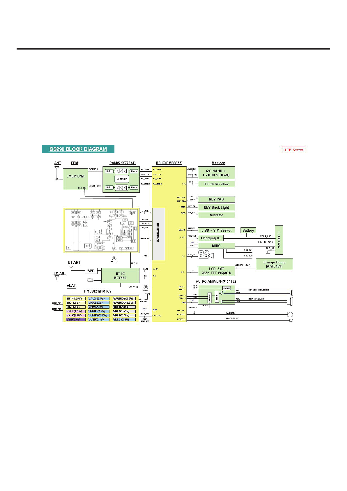
3.1. GS290 Functional Block diagram.
The functional component arrangement is mentioned below diagram.
Figure 1 GS290 Functional block diagram
3. TECHNICAL BRIEF
Copyright © 2010 LG Electronics. Inc. All right reserved.
Only for training and service purposes
- 17 -
LGE Internal Use Only
3. TECHNICAL BRIEF
GS290 Operational Description Revision B
3.2. Baseband Processor (BBP) Introduction
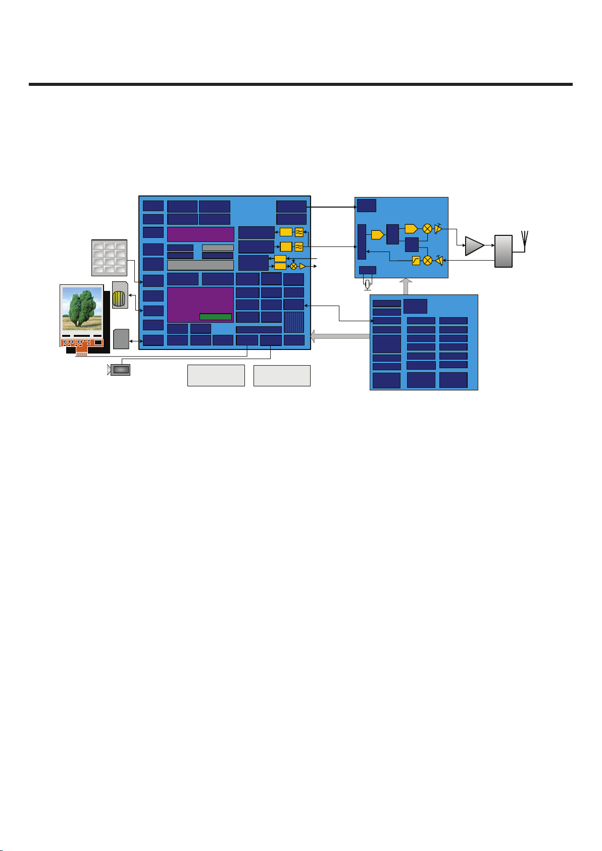
S-GOLD3 Baseband IC
PMB 8877
S-GOLD3 Overview
TM
is a GSM/EDGE single chip mixed signal baseband IC containing all analog and digital functionality
TM
provides multimedia extensions to enable today’s and future feature
TM
supports multislot operation modes
TM
is handled by an ARM926EJ-S CPU and a TEAKLite® DSP core.
TM
Quad-Band E-GPRS Solution
SMARTiPM
PMB 6272
(EDG E GSM/GPR S RF Tran sceiver)
TEAKL ite®
GEA-1/2/3
SRA M
USB FS
OTG
DMA C
GPIO s
USIM
GPTU
RTC
Equali zer
Acc.
I²S / DAI
GSM
Timer
Keyp ad
AFC
CAPCO M
IC U
SPCU
AUX
ADC
SRC
MEM
CTRL
SDIO I F
I²C
CGU
Display
IF
Camera
IF
FCDP
Multi media I C IF
ARM® 926 EJ-S
MOVE CoPro
Fast
IrDA
USIFs
Cryp to
box
TSMU
I²S
Sys
Timer
1 Wire
Engi ne
2D
MMC IF
Channel
Deco der
BB Receiver
Modu lator
8 PSK/GMSK
JTAG
Cerb erusABW
S-GOLD3
PMB 8877
IR-Memory
DAC
ADC
Audio FE
DAC
DSP
Timer
DSP
ICU
DSP
ICU
ADC
I/Q
DA C
Ph/
Am p
SD
PLL
IF
AD C
3 WIRE
IF
RF
Control IF
GSM
Cipher Unit
3-wire- bus
Analog
Audio In
Analog
Audio Out
SDs
SM-Power3
PMB 6821
USB
AU DIO
AMPL IFIER
BA CK LIGHT
I²C
DI GITA L
CO NTR OL
CH AR GER
DI G. R ESET
& SLEEP
CO NTR OL
VRF sVAU DIO s
VMMCVUSB
VSIMVRT C
VVIBVAU X
VAF C
SU
VIOVPLL
REF ERENC E
PA
FEM
DC XO
Core supply (0.95 V,1 .37V)
Analog Supply(2.5V)
VRTC, VPLL, IO Supply
1.8V, 2.5V
LD Os
FLA SH
LIG HT
SDR or D DR
SD-R AM
/ C -RA M
NO R / NAN D
FLA SH
1 32
4 65
7 98
* #0
SIM
MMC
GS290 Operational Description Revision B
3.2. Baseband Processor (BBP) Introduction
Figure 2 Top level block diagram of the S-GOLD3TM (PMB8877)
LGE Internal Use Only Copyright © 2010 LG Electronics. Inc. All right reserved.
- 18 -
Only for training and service purposes

3. TECHNICAL BRIEF
GS290 Operational Description Revision B
3.2.1. General Description
S-GOLD3TM is a GSM/EDGE single chip mixed signal Baseband IC containing all analog and digital functionality
of a cellular radio. Additionally S-GOLD3TM Provides multimedia extensions such as camera, software MIDI, MP3
sound. It is designed as a single chip solution, integrating the digital and mixed signal portions of the base
band in 0.09um, 1.2V technology.
The chip will fully support the FR, EFR, HR and AMR-NB vocoding.
S-GOLD3
TM
support multi-slot operation modes HSCSD (up to class 10), GPRS for high speed data application
(up to class 12) and EGPRS (up to class 12) without additional external hardware.
3.2.2. Block Description
z Processing core
ARM926EJ-S 32 bit processor core for controller functions. The ARM926EJ-S includes an MMU, and the Jazelle
Java extension for Java acceleration.
- TEAKLite DSP core
z ARM-Memory
- 32k Byte Boot ROM on the AHB
- 96k Byte SRAM on the AHB, flexibly usable as program or data RAM
- 16k Byte Cache for Program (internal)
- 8k Byte tightly coupled memory for Program(internal)
- 8k Byte Cache for Data(internal)
- 8k Byte tightly coupled memory for Data(internal)
z DSP-Memory
- 104K x 16bit Program ROM
- 8k x 16bit Program RAM
- 60k x 16bit Data ROM
- 37k x 16bit Data RAM
- Incremental Redundancy(IR) Memory of 35904 words of 16bit
z Shared Memory Block
1.5K x 32bit Shared RAM(dual ported) between controller system and TEAKLite.
z Controller Bus system
The processor cores and their peripherals are connected by powerful buses.
Multi-layer AHB for connecting the ARM and the other master capable building blocks with the internal and
external memories and with the peripheral buses.
Copyright © 2010 LG Electronics. Inc. All right reserved.
Only for training and service purposes
- 19 -
LGE Internal Use Only

3. TECHNICAL BRIEF
GS290 Operational Description Revision B
z Clock system
The clock system allows widely independent selection of frequencies for the essential parts of the S-GOLD3.
Thus power consumption and performance can be optimized for each application.
z Functional Hardware block
- CPU and DSP Timers
- MOVE coprocessor performing motion estimation for video encoding algorithms
(H.263, MPEG-4)
- Programmable PLL with additional phase shifters for system clock generation
- GSM Timer Module that off-loads the CPU from radio channel timing
- GMSK / 8-PSK Modulator according to GSM-standard 05.04 (5/2000)
- GMSK Modulator: gauss-filter with B*T=0.3
- EDGE Modulator: 8PSK-modulation with linearized GMSK-Pulse-Filter
- Hardware accelerators for equalizer and channel decoding.
- Incremental Redundancy memory for EDGE class 12 support
- A5/1, A5/2, A5/3 Cipher unit
- GEA1, GEA2, GEA3 Cipher Unit to support GPRS data transmission
- Advanced static and dynamic power management features including TDMA-Frame
synchronous low power mode and enhanced CPU modes(idle and sleep modes)
- Pulse Number Modulation output for Automatic Frequency Correction(AFC)
- Serial RF Control interface: support of direct conversion RF
- A Universal Serial Interface(USIF) enabling asynchronous (UART) of synchronous (SPI)
serial data transmission
- 3 USIF with autobaud detection, hardware flow control and integrated
- A dedicated Fas IfDA Controller supporting IrDA’s SIR,MIR and FIR standards
(up to 4Mbps)
- I2C-bus interface (e.g. connection to S/M power)
- A fast display interface supporting serial and parallel interconnection
- An ITU-R BT.656 compatible Camera interface.
- Programmable clock output for a camera
- An multimedia/Secure Digital Card Interface (MMCI/SD:SDIO capable)
LGE Internal Use Only Copyright © 2010 LG Electronics. Inc. All right reserved.
- 20 -
Only for training and service purposes
3. TECHNICAL BRIEF
GS290 Operational Description Revision B
3.2.3. External Devices connected to memory interface
Table 1. Memory interface
Device Name Maker Remark
FLASH K522H1HACB-B060 SAMSUNG Synchronous / A synchronous
DDR K522H1HACB-B060 SAMSUNG Synchronous 166MHz
LCD IM300IBN1A LGIT 8bit access 2 times transmission
Melody IC Not Used S/W Infineon Software CODEC
3.2.4. RF Interface (T_OUT)
S-Gold3 uses this interface to control RF IC and Peripherals. 13 signals are provided switch on/off RF ICs
Periodically each TDMA frame.
Table 2. RF Interface Spec.
T_OUT
Resource Interconnection Description
T_OUT0 TXON_PA PAM Power on
T_OUT1 N/A N/A
T_OUT2 PA_BAND TX RF band select
T_OUT3 N/A N/A
T_OUT4 N/A N/A
T_OUT5 Other function -
T_OUT6 PA MODE PAM Mode select
3.2.5. USIF Interface
GS290 have three USIF Drivers as follow :
- USIF1 : Hardware Flow Control / SW upgrade / Calibration
- USIF2 : Not used Rx, Tx and CTS, RTS use BT Interface
- USIF3 : BT Interface
Copyright © 2010 LG Electronics. Inc. All right reserved.
Only for training and service purposes
- 21 -
LGE Internal Use Only

3. TECHNICAL BRIEF
GS290 Operational Description Revision B
Table 3. USIF Interface Spec.
3.2.6. ADC channel
BBP ADC block is composed of 10 external ADC channel. This block operates charging process and other
related process by reading battery voltage and other analog values.
Table 4. S-Gold3 ADC channel usage
ADC channel
Resource Interconnection Description
M0 BAT_ID Battery temperature measure
M1 RF_TEMP RF block temperature measure
M2 N.C
M3 N.C
M4 N.C
M5 N.C
M6 N.C
M7 N.C
M8 VSUPPLY Battery supply voltage measure
M9 N.C
M10 N.C
Resource Name Remark
USIF1
USIF1_TXD TXD Transmit Data
USIF1_RXD RXD Receive Data
USIF1_CTS USB_DP
USIF1_RTS USB_DM
USIF2
USIF2_TXD NC NC
USIF2_RXD Other function USIF2_CTS BT_CTS
USIF2_RTS BT_RTS.
USIF3
USIF3_TXD BT_TX BT Transmit tx
USIF3_RXD BT_RX BT Receive rx
LGE Internal Use Only Copyright © 2010 LG Electronics. Inc. All right reserved.
- 22 -
Only for training and service purposes
3. TECHNICAL BRIEF
GS290 Operational Description Revision B
3.2.7. GPIO map
Over a hundred allowable resources, GS290 is using as follows except dedicated to SIM and Memory. GS290
GPIO(General Purpose Input/Output) Map, describing application, I/O state, and enable level, is shown in below
table
GS290 Operational Description Revision B
3.2.7. GPIO map
Over a hundred allowable resources, GS290 is using as follows except dedicated to SIM and Memory. GS290
GPIO(General Purpose Input/Output) Map, describing application, I/O state, and enable level, is shown in below
table
Table 5 S-Gold3 GPIO pin Map
Port Function Net Name Description
KEY MATRIX
KP_IN0
KP_IN1
KP_IN2
KP_IN3
KP_IN(3)
KP_IN4
KP_IN5
KP_IN(5)
KP_IN6
KP_IN(6)
KP_OUT0
BT_HOST_WAKEUP
KP_OUT1
KP_OUT(0)
KP_OUT2
KP_OUT(2)
KP_OUT3
KP_OUT(3)
USIF1
USIF1_RXD
UART_RX UART, RS232 Data
USIF1_TXD
UART_TX UART, RS232 Data
USIF1_RTS_N
USB_DAT_VP USB Data
USIF1_CTS_N
USB_SE0_VM USB Data
USIF2
USIF2 _RXD
USW_INT MUIC Interrupt Singnal
USIF2 _TXD
NA Not used
USIF2_RTS_N
UART_BT_RTS Bluetooth RTS
USIF2_CTS_N
UART_BT_CTS Bluetooth CTS
USIF3
USIF3 _RXD
UART_BT_RX Bluetooth RX
USIF3 _TXD
UART_BT_TX Bluetooth TX
CLK
CLK32K
CLK32k For FM Radio, BT CLK32K
GPIO_22
Not used
CAMERA I/F
Copyright © 2010 LG Electronics. Inc. All right reserved.
Only for training and service purposes
- 23 -
LGE Internal Use Only
3. TECHNICAL BRIEF
GS290 Operational Description Revision B
CIF_D0
CIF_D(0) Camera DATA[0]
CIF_D1
CIF_D(1) Camera DATA[1]
CIF_D2
CIF_D(2) Camera DATA[2]
CIF_D3
CIF_D(3) Camera DATA[3]
CIF_D4
CIF_D(4) Camera DATA[4]
CIF_D5
CIF_D(5) Camera DATA[5]
CIF_D6
CIF_D(6) Camera DATA[6]
CIF_D7
CIF_D(7) Camera DATA[7]
CIF_PCLK
CIF_PCLK Camera pixel clock
CIF_HSYNC
CIF_HS Camera H sync
CIF_VSYNC
CIF_VS Camera V sync
CLKOUT
CIF_MCLK Camera main clock
CIF_PD
CIF_PD Camera power down(active high)
CIF_RESET
CIF_RESET Camera reset
LCD I/F
DIF_D0
DIF_D(0) LCD data[0]
DIF_D1
DIF_D(1) LCD data[1]
DIF_D2
DIF_D(2) LCD data[2]
DIF_D3
DIF_D(3) LCD data[3]
DIF_D4
DIF_D(4) LCD data[4]
DIF_D5
DIF_D(5) LCD data[5]
DIF_D6
DIF_D(6) LCD data[6]
DIF_D7
DIF_D(7) LCD data[7]
DIF_D8
DIF_D(8) LCD data[8]
DIF_CS1
DIF_MAIN_CS MAIN LCD chip select
DIF_CS2
IF_MODE LCD Interface mode
DIF_CD
DIF_CD Command Data switch
DIF_WR
DIF_WR LCD Write
EINT7
HOOK_DETECT Ear-Mic hook detection
DIF_RESET1
_DIF_RESET LCD Reset
GPIO_108
VIB_EN Vibrator enable
I2C
I2C_SCL
I2C_SCL For PMIC/Amp/Touch/MUIC
I2C_SDA
I2C_SDA For PMIC/Amp/Touch/MUIC
PM_INT (EINT)
PM_INT
LGE Internal Use Only Copyright © 2010 LG Electronics. Inc. All right reserved.
- 24 -
Only for training and service purposes
3. TECHNICAL BRIEF
GS290 Operational Description Revision B
SIM I/F
CC_IO
SIM_IO SIM CARD I/O
CC_CLK
SIM_CLK SIM CARD CLOCK
CC_RST
SIM_RST SIM CARD RESET
I2S2
I2S2_CLK0
Not used
GPIO_102
LCD ID LCO Bender Check
I2S2_RX
Not used
I2S2_TX
Not used
I2S2_WA0
Not used
GPIO_103
Not used
External Memory
MMCI_CMD
TF_CMD T-flash
MMCI_DAT[0]
TF_DAT0 T-flash
MMCI_CLK
TF_CLK T-flash
GPIO_109
CAM_LDO_EN Camera Power LDO Control
IrDA
GPIO_110
GPIO_109
I2S1
I2S1_CLK0
BT_PCM_CLK For Bluetooth
I2S1_CLK1
MMC_DETECT T-flash Detect
I2S1_RX
I2S1_RX For Bluetooth
I2S1_TX
I2S1_TX For Bluetooth
I2S1_WA0
I2S1_WA For Bluetooth
External Memory
MMCI_DAT[1]
TF_DAT1 T-flash
MMCI_DAT[2]
TF_DAT2 T-flash
MMCI_DAT[3]
TF_DAT3 T-flash
Audio I/F
EPN1
EAR_N For Receiver
EPP1
EAR_P For Receiver
EPPA1
BBP_SND_L For Speaker
EPREF
Reference
Copyright © 2010 LG Electronics. Inc. All right reserved.
Only for training and service purposes
- 25 -
LGE Internal Use Only
3. TECHNICAL BRIEF
GS290 Operational Description Revision B
EPPA2
BBP_SND_R For Speaker
MICN1
MIC1_N For Mic
MICP1
MIC1_P For Mic
MICN2
MIC2_N For Headset Mic
MICP2
MIC2_P For Headset Mic
VMICP
VMICP Power for MIC
VMICN
VMICN Power for MIC
ADC
M0
BAT_ID Battery temperature measure
M1
RF_TEMP RF block temperature measure
M2
M3
M7
M8
VSUPPLY Battery supply voltage measure
M9
M10
Reference
VREF
IREF
JTAG I/F
TDO
TDO JTAG
TDI
TDI JTAG
TMS
TMS JTAG
TCK
TCK JTAG
TRST_n
_TRST JTAG
RTCK
RTCK JTAG
ETM I/F
TRIG_IN
TRIG_IN ETM (Embedded Trace Macro Cell)
MON1
MON1 ETM
MON2
MON2 ETM
TRACESYNC
TRACESYNC ETM
TRACECLK
TRACECLK ETM
PIPESTAT[2]
PIPESTAT2 ETM
PIPESTAT[1]
PIPESTAT1 ETM
PIPESTAT[0]
PIPESTAT0 ETM
LGE Internal Use Only Copyright © 2010 LG Electronics. Inc. All right reserved.
- 26 -
Only for training and service purposes
3. TECHNICAL BRIEF
GS290 Operational Description Revision B
TRACEPKT[0]
TRACEPKT(0) ETM
TRACEPKT[1]
TRACEPKT(1) ETM
TRACEPKT[2]
TRACEPKT(2) ETM
TRACEPKT[3]
TRACEPKT(3) ETM
TRACEPKT[4]
TRACEPKT(4) ETM
TRACEPKT[5]
TRACEPKT(5) ETM
TRACEPKT[6]
TRACEPKT(6) ETM
TRACEPKT[7]
TRACEPKT(7) ETM
Memory
MEM_AD[0]
DATA(0)
MEM _AD[1]
DATA (1)
MEM _AD[2]
DATA (2)
MEM _AD[3]
DATA D(3)
MEM _AD[4]
DATA (4)
MEM _AD[5]
DATA (5)
MEM _AD[6]
DATA (6)
MEM _AD[7]
DATA (7)
MEM _AD[8]
DATA (8)
MEM _AD[9]
DATA (9)
MEM _AD[10]
DATA (10)
MEM _AD[11]
DATA (11)
MEM _AD[12]
DATA (12)
MEM _AD[13]
DATA (13)
MEM _AD[14]
DATA (14)
MEM _AD[15]
DATA (15)
MEM _WR_n
_WR
MEM _RD_n
_RD
MEM _BC0_n
_BC0
MEM _BC1_n
_BC1
MEM _A[0]
ADD(0)
MEM _A[1]
ADD (1)
MEM _A[2]
ADD (2)
MEM _A[3]
ADD (3)
MEM _A[4]
ADD (4)
MEM _A[5]
ADD (5)
Copyright © 2010 LG Electronics. Inc. All right reserved.
Only for training and service purposes
- 27 -
LGE Internal Use Only

3. TECHNICAL BRIEF
GS290 Operational Description Revision B
MEM _A[6]
ADD (6)
MEM _A[7]
ADD (7)
MEM _A[8]
ADD (8)
MEM _A[9]
ADD (9)
MEM _A[10]
ADD (10)
MEM _A[11]
ADD (11)
MEM _A[12]
ADD (12)
MEM _A[13]
ADD (13)
MEM _A[14]
ADD (14)
MEM _A[15]
ADD (15)
MEM _A[16]
ADD (16)
MEM _A[17]
ADD (17)
MEM _A[18]
ADD (18)
MEM _A[19]
ADD (19)
MEM _A[20]
ADD (20)
MEM _A[21]
ADD (21)
MEM _A[22]
ADD (22)
MEM _A[23]
ADD (23)
MEM _A[24]
ADD (24)
MEM_A[25] ADD(25)
MEM_A[26] ADD(26)
MEM_CSA0_n ADD(27)
MEM_CSA1_n ADD(28)
MEM_CSA2_n ADD(29)
MEM _RAS_n
_RAS
MEM _CAS_n
_CAS
MEM _WAIT_n
_WAIT
MEM _SDCLKO
SDCLKO For Burst mode
MEM _SDCLKI
SDCLKI For Burst mode
MEM _BFCLKO
BFCLKO For Burst mode
MEM _BFCLKI
BFCLKI For Burst mode
MEM _CKE
CKE
Memory
FCDP_RBn
FCDP
TDMA I/F
LGE Internal Use Only Copyright © 2010 LG Electronics. Inc. All right reserved.
- 28 -
Only for training and service purposes

3. TECHNICAL BRIEF
GS290 Operational Description Revision B
T_OUT0
TXON_PA PAM
GPIO_108
VIB_EN
T_OUT2
PA_BAND PAM
T_OUT3
FE1
T_OUT4
BT_WAKEUP
T_OUT5
LIN_PWM_MAG
T_OUT6
PA_MODE PAM
T_OUT7
LIN_PWM_FRQ
CC1CC7IO
JACK_DETECT
GPIO_52
LCD_BACKLIGHT LCD Backlight control
GPIO_102
LCD_ID LCD ID check
GPIO_54
RF I/F
RF_STR0
RF_EN
CC1CC5IO
_PPR For Charger
RF_DATA
RF_DA
RF_CLK
RF_CLK
System Port
AFC
AFC
CLKOUT0 [<=26MHz]
Not used
F26M
26MHZ_MCLK 26M Main Clock
F32K
to 32k crystal
OSC32K
to 32k crystal
RESET_n
_RESET
TRIG_OUT
TRIG_OUT
RTC_OUT
RTC_OUT
VCXO_EN
VCXO_EN
DSP
GPIO_61
GPIO_62
GPIO_63
Copyright © 2010 LG Electronics. Inc. All right reserved.
Only for training and service purposes
- 29 -
LGE Internal Use Only

3. TECHNICAL BRIEF
GS290 Operational Description Revision B
3.3. Power management IC
3.3.1. General Description
SM-POWER is a highly integrated Power and Battery Management IC for mobile handsets. It has been specially
designed for usage with S-Gold3. Although optimized for usage with the Infineon S-GOLD baseband device it
is suitable for the S-GOLDlite and the E-GOLD+ baseband devices as well. It also supports the cellular RF
devices like SMARTi-DC, SMARTi-DC+, SMARTi-SD and the Bluemoon Single, Infineon’s single chip solution for
Bluetooth. If used with S-GOLD3 it provides all power supply functions (except for the RF PA) for a complete
advanced GSM Edge smart phone minimizing external device count.
Block Description
• Highly efficient step-down converter for main digital baseband supply including Core, DSP and
memory interface (External Bus Unit).
• Support of S-GOLD standby power-down concept
• Low-drop-out (LDO) regulators for Flash and mobile RAM memory devices
• Voltage independent switching of two SIM cards
• LDO regulators for baseband I/O supply
• LDO regulator for analog mixed-signal section of S-GOLD
• Low-noise LDO regulators for RF devices
• Supply for Bluemoon Single, Infineon’s single chip solution for Bluetooth
• Audio amplifier 8 Ohms for handsfree operation and ringing
• Charge Control for charging Li-Ion/Polymer batteries under software control
• Pre-charge current generator with selectable current level
• RTC regulator with ultra-low quiescent current
• USB interface support for peripheral and mini-host mode
• Backlight LEDs driver with current selection and PWM dimming function
• Two single LED driver outputs for signaling
• Vibrator driver with adjustable voltage
• Fully controlable by software via I2C – Bus
• Temperature and battery voltage sensors
• Interrupt channels for peripherals
• System debug mode
• VQFN 48 package with heat sink and non-protruding leads
• Compatible with the Infineon E-GOLD+ V2 and V3
LGE Internal Use Only Copyright © 2010 LG Electronics. Inc. All right reserved.
- 30 -
Only for training and service purposes

3. TECHNICAL BRIEF
GS290 Operational Description Revision B
SM-POWER is a further step on the successful E-Power product line with enhanced and optimized functionality.
SM-POWER features a baseband supply concept with a DC/DC step-down converter cascaded by two linear
regulators
–SM-POWER’s DC/DC converter makes up to 40 % reduction of battery current for smart phone functions (e.g.
organizer functions, games, MP3 decoding) possible.
– SDBB has high efficiency up to 95% and also a power save mode.
– Memory Interface is directly supported by the SDBB
– SDBB can also act as main supply voltage for E-GOLD+ or S-GOLDlite baseband devices.
– For S-GOLD two linear regulators for DSP and Core are cascaded after the SDBB.
SM-POWER supports the standby power-down concept of S-GOLD by temporarily switching off the linear
regulator for the DSP during mobile standby whenever this subsystem is not used. In this phase the ARM
controller and most peripherals including parts of the on-chip SRAM are kept powered-up with power being
supplied by the other linear regulator.
SM-POWER includes a fully differential audio amplifier able to drive loads down to a nominal value of 8 Ohm for
usage in hands-free phones and for ringing
– 450 mW maximum output power
– adjustable gain
– mute switch SM-POWER also integrates a charging function for Li-Ion, Li-Polymer batteries
– click and pop -protection SM-POWER also integrates a charging function for Li-Ion, Li-Polymer batteries
– Precharge current source with two current levels
– Constant current / constant voltage charging with 3 different termination voltages
– Programable charge current limitation for use with different batteries
– Freely programable pulse charging to reduce the thermal power dissipation in the constant voltage
charging phase
– Top-off charge current sensing SM-POWER completes the USB interface of S-GOLD
– Regulated voltage for S-GOLD USB interface including reverse current and overvoltage protection
– Switch to supply USB pull-up resistor
– Mini-host pull down resistor functionality
– Charge pump with internal switching capacitor for USB host VBUS supply voltage SM-POWER fully supports
LED and Vibra Motor functionality
– no external components needed
– driver for backlight LEDs adjustable in steps up to 140mA and with soft turn on and off by PWM dimming
– two driver outputs for single LEDs for precharge indication and signaling with i.e. change of colour
Copyright © 2010 LG Electronics. Inc. All right reserved.
Only for training and service purposes
- 31 -
LGE Internal Use Only

3. TECHNICAL BRIEF
GS290 Operational Description Revision B
–driver for Vibra Motor with adjustable voltages, soft startup / shutdown and current limitation
SM-POWER offers several control functions
– Power-on Reset Generator with logic state machine
– I2C bus interface
– I2C bus configurable mode control logic with ON (push-button or RTC), VCXOEN and LRF3EN (wake-up by
Bluetooth) inputs
– Programable interrupt channels to handle peripherals like SIM, MMC and USB
– Monitoring of charging functions
– Undervoltage Shut-Down
– Errorflags (volatile or non-volatile) from many power-supply functions and thermal sensor in order to debug
system
– Overtemperature Shut-Down
– Overtemperature Warning
– Support of S-GOLD standby power-down concept
– Support of S-GOLD Power-Down Pad Tristate Function
Table 6. LDO Output Table of SM-Power
LDO Net name Output Voltage Output Current Usage
SD1 1V35_Core 1.35V 600mA Core & for LDO
SD2 1V8_SD 1.8V 300mA Memory
VAUX 2V9_VAF 2.9V 100mA Cam Auto Focus
VIO 2V62_VIO 2.62V 100mA Peripherals
VSIM 2V9_SIM 2.9V 70mA SIM card
VMME 2V8_VMME 2.9V 150mA u-SD
VUMTS 2V85_AMP 2.85V 110mA Headset AMP
VUSB VUSB 3.1V 40mA VUSB
VLED VLED 2.9V 10mA Not used
VAUDIOa 2V5_VAUDA 2.5V 200mA Stereo headset, Mono earpiece
VAUDIOb 2V5_VAUDB 2.5V 50mA Analog parts of S-Gold
VRF1 2V85_VRF 2.85V 150mA
2.85 V supply for SMARTi-PM
RF transceiver
VRF2 1V5_VRF 1,53V 100mA
1.5 V supply for SMARTi-PM
RF transceiver
VRF3 2V65_VBT 2.7V 150mA Bluetooth
VPLL 1V35_VPLL 1.35V 30mA S-GOLD3 PLL
VRTC 2V11_RTC 2.11V 4mA Real Time Clock
VAFC VAFC 2.65V 5mA Not used
VVIB 2V8_VLCD 2.8V 140mA LCD
GS290 Operational Description Revision B
–driver for Vibra Motor with adjustable voltages, soft startup / shutdown and current limitation
SM-POWER offers several control functions
– Power-on Reset Generator with logic state machine
– I2C bus interface
– I2C bus configurable mode control logic with ON (push-button or RTC), VCXOEN and LRF3EN (wake-up by
Bluetooth) inputs
– Programable interrupt channels to handle peripherals like SIM, MMC and USB
– Monitoring of charging functions
– Undervoltage Shut-Down
– Errorflags (volatile or non-volatile) from many power-supply functions and thermal sensor in order to debug
system
– Overtemperature Shut-Down
– Overtemperature Warning
– Support of S-GOLD standby power-down concept
– Support of S-GOLD Power-Down Pad Tristate Function
LGE Internal Use Only Copyright © 2010 LG Electronics. Inc. All right reserved.
- 32 -
Only for training and service purposes

3. TECHNICAL BRIEF
GS290 Operational Description Revision B
Fi
Figure 3. SM-Power Circuit Diagram of GS290
22u
C234
0.1u
C204
C200
1u
u2.
2
1
0
2C
VAUDA_2V5
C202
2.2u
SD_1V8
u01
0
0
2L
VBAT
302C u1
0.1u
C214
VFM_2V9
1u
C2051uC207
VRF_1V5
10u
L201
10u
C208
2.2u
C209
VPLL_1V35
u1112C
VBAT
CORE_1V35 CAM_A_2V8
U202
PMB6821
4H
8H9D6J
7H6H5H
9G8G7G6G5G4G3G9F8F
7F6F5F4F3F9E
8
E
7E
6E
5E
4E8D7D6D5D4D
6C
L2
L10K2
J10K1
K11
J3
J11H3
H9J2
J1
H10
H1
H11H2
G10G1
G2
G11
F11F1
F10F2
E11E1
E10E2
D1
D11E3
D10
D2
C10C1
C11D3
C2
B1
11L
8A
9J
01K
9L
9K8L8K
7L
8J7K6L
7J6K5K5J5L4L4K3L3K
4J1A4B
11B
1L
11A
9B
01A
0
1B9C9A
8C8B6A7C7A5A7B
5C6B5B4A4C
3A
3B3C2A
2B
MV_0ES
PV_TAD
-CA
+CA
DNEPSUS
N_EO
BSUV
BSU_DDV
P
NI_
O
NOM
NNI_ONOM
ONOM_DDV
M_XEFE
RV
P
TUO_ONO
M
ONOM_SSV
N
TUO_ONO
M
FERR
FERV
KN
I
HS_HSALF
NO_HSALF
APNOXT
LLPV
OILLPDDV
O
IV
2DSV
3SMUP
2SMUP
1SMUP
TROPTUO
NO_REWOP
GODW
1FFO_NO
2FFO_NO
TUO_FFO_NO
LTRC_ECRUOSER
TNI_C2I
TAD_C2I
KLC_C2I
MWP_1LB
MWP_2LB
MWP_3LB
LRTNC_HC
ECRUOS_HC
CU_EGRAHC
EGRAHC_DDV
1NI_ESNES
2NI_ESNES
FER_DDV
DELV
1DSV
RCV
VPIN
VMIN VMME
D+ VDDMME
D-
VDDRF2
RESET_N VRF2
RESET2_N
SLEEP1_N VRF3
SLEEP2_N VDDRF13_AFC
VAUDIOA VRF1
VDDAUDIOA VVIB
VDDSIMVIB
VDDAUDIOB
VAUDIOB VSIM
VAUX VAFC
VDDAUX
VRTC
SU1_GATE
SU1_GND VDDUMTS
SU1_FB VUMTS
SU1_ISENSE
VDDSD1
VDDSD2 SD1_FB
SD2_FB SD1_FBL
SD2_FBL
1SSV
2SSV
3SSV
4SSV
5SSV
6SSV
7SSV
8SSV
9SSV
01SSV
11SSV
21SSV
3
1SSV
41SSV
51SSV
61SSV
7
1SSV
81SSV
91SSV
02SSV
12SSV
22SSV
32SSV
42SSV
52SSV
62SSV
72SSV
82SSV
92SSV
03SSV
FERV_SSV
1DS_SSV
2DS_SSV
u1.0
7
1
2C
u01512C
612C
u01
VBAT
u1.0
3
32
C
CAM_2V85
402R
K7.4
1u
C219
C222
10u
1u
C223
522C
u01
312R
IND
R214
27K
VAUDB_2V5
C226
2.2u0.1u
C227
H-KTRE061SDK
002D
002PT
VBAT
512R K001
VIO_2V62
C228
1u
102PT
612R
K001
VSIM_2V9
2.2u
C229
VBAT
1u
C230
RTC_2V11
2.2u
C231
VBT_2V65
232C
u1
VRF_2V85 VMME_2V9
VBAT
1u
C235
FB201
A122S8
0
6
1
ZPM 0
2
2
2
0
2B
F
A122S8061ZPM
VUSB
1u
C236
1u
C237
2.2u
C238
SD_1V8
C239
2.2u
202PT
VBAT
C240
2.2u
VBAT
C241
1u
VBAT
K7.4
122R
K001
722R
H-KTRE061SDK
102D
USB_SE0_VM
NE_YEK
GODW
USB_OEN
VCXO_EN
TXON_PA
ADS_C2I
LCS_C2I
RTC_OUT
USB_DAT_VP
LRTC_ECRUOSER
USB_DP
USB_DM
RPWRON_EN
2FFO_NO
ON_OFF2
NORWP
TNI_REWOPS
LB_YEK
PMRSTN
FM_SPK_INN
FM_SPK_INP
FM_SPK_OUTP
FM_SPK_OUTN
BT_CLK_REQ
PMIC
K3.3
6
0
2R
SC200
21
GU073-5P-SD-E1500
CN200
15
13
11
9
7
5
4
3
2
1
14
12
10
8
6
BQ25040
U201
5 6
74
83
92
101
11
PGND
IN BAT
ISET _PG
VSS1 CHG
LDO VSS2
EN_SETIFULL
1u
C2101uC212
VIO_2V62
VIO_2V62
502R
IND
V_BUS
C220
22pDNI
C221
C224
1u
VBATVIO_2V62
V_BUS
K001
322R
0
2
8
702R
K001
422R
_CHG_EOC
_PPR
_CHG_EN
RPWRON_EN
USW_ID
USW_DP
USW_DM
Single Charging IC for uUSB
)%
1(
(645mA)
)%1
(
(105mA)
Micro USB
GS290 Operational Description Revision B
Fi
Figure 4 charging part
Copyright © 2010 LG Electronics. Inc. All right reserved.
Only for training and service purposes
- 33 -
LGE Internal Use Only

3. TECHNICAL BRIEF
GS290 Operational Description Revision B
3.3.2. Charging
The bq25040 has a single power output that charges the battery. A system load can be placed in parallel with
the battery.The charge current is programmed using the ISET and EN/SET inputs. The charge current is
programmable to USB100, USB500 or a user programmed charge current up to 1.2A. Additionally, a 4.9V +/-3%
50mA LDO is integrated into the IC for supplying low power external circuitry. The one-wire interface (EN/SET)
is available to place the bq25040 into Test Jig Mode. In Test Jig Mode, the output is regulated at 4.2V and can
be used without a battery.The bq25040 has a single power output that charges the battery.. Either a 1-cell
Li-Ion or Li-Ion-Polymer battery with 4.1, 4.2 or 4.4 Volts may be used.
4.2V~3.74V 3.73V~3.65V 3.65V~3.59V 3.59V~3.35V
Figure 5 Battery Block Indication
1. Charging method : CC-CV
2. Charger detect voltage : 4.8 V
3. Charging time : 2h
4. Charging current : 645 mA
5. CV voltage : 4.2 V
6. Cutoff current : 105 mA
7. Full charge indication current (icon stop current) : 110 mA
8. Recharge voltage : 4.16 V
9. Low battery alarm
a. Stand by : 3.59V˨ ±0.05V
b. Call : 3.59V˨ ±0.05V
10. Low battery alarm interval
a. Stand by : 3 min
b. Dedicated : 1 min
11. Switch-off voltage : 3.35 V
LGE Internal Use Only Copyright © 2010 LG Electronics. Inc. All right reserved.
- 34 -
Only for training and service purposes

3. TECHNICAL BRIEF
GS290 Operational Description Revision B
3.4. Power ON/OFF
GS290 Power State : Defined 3cases as follow
ඖ Power-ON : Power key detect (SM-Power’s ON port)
ඖ Power-ON-charging : Charger detect.
Figure 6 Power on application.
Copyright © 2010 LG Electronics. Inc. All right reserved.
Only for training and service purposes
- 35 -
LGE Internal Use Only

3. TECHNICAL BRIEF
GS290 Operational Description Revision B
3.4. Power ON/OFF
GS290 Power State : Defined 3cases as follow
ඖ Power-ON : Power key detect (SM-Power’s ON port)
ඖ Power-ON-charging : Charger detect.
Figure 6 Power on application.
Input ON is a power-on input for SM-POWER with 2 active high levels (see Figure 6). It might be triggered by a
push button or by the RTCOUT output of the S-GOLD device as well. To detect if the push-button is pressed
during system operation the logical level at pin ON or its change (if Bit 1 EION in INTCTRL2 is asserted) is
recorded in bit LON of the ISF register. If the high level of voltage at pin ON does not reach VIHdet (Vbat-0.8 ~
Vbat-0.3) the above-mentioned bit won’t be set.
To support Remote power on function for factory mass production, applied an analog switch as following
figure. As monitoring the RPWRON and Key matrix KP_OUT(2) & KP_IN (6), GS290 system recognize whether
remote power on or End-key pushed
GS290 Operational Description Revision B
Figure 7 Remote power on and End-key power on circuit
Q201
1
2
3
Q200
1
2
3
K03
1
2
1
2R
7
12
R
K57
K
001
222R
10K
R226
82
2
R
K2
RTC_2V11
KP_OUT[2]
RPWRON
KP_IN[6]
RPWRON_EN
END
PWRON
END_KEY_IN
END_KEY_IN
Power On
LGE Internal Use Only Copyright © 2010 LG Electronics. Inc. All right reserved.
- 36 -
Only for training and service purposes

3. TECHNICAL BRIEF
GS290 Operational Description Revision B
Figure 7 Remote power on and End-key power on circuit
3.5. SIM & uSD interface
GS290 supports 1.8V & 2.9V plug in SIM, SIM interface scheme is shown in (Figure 8).
SIM_IO, SIM_CLK, SIM_RST ports are used to communicate with BBP(S-Gold3) and the SIM power supply
enabled by PMIC.
SIM Interface
SIM_CLK : SIM card reference clock
SIM_RST : SIM card Async /sync reset
SIM_IO : SIM card bidirectional reset
Figure 8 SIM & Micro SD Circuit
GCA26D-6S-H18-E1500
J400
9 8
10 7
6 3
5 2
4 1
C1C5
C2C6
C3C7
GND1GND4
GND2GND3
0.1u
C401
VSIM_2V9 VSIM_2V9
R407
10K
22p
C405
C409
DNI
C410
22p
VSIM_2V9
SIM_RST
SIM_IO SIM_CLK
SIM CONNECTOR
Copyright © 2010 LG Electronics. Inc. All right reserved.
Only for training and service purposes
- 37 -
LGE Internal Use Only

3. TECHNICAL BRIEF
GS290 Operational Description Revision B
The MicroSD Memory Module has eight exposed contacts on one side. The S-Gold3 is connected to the module
using a dedicated eight-pin connector
Micro SD Memory Card Detection Scheme
GS290 Operational Description Revision B
The MicroSD Memory Module has eight exposed contacts on one side. The S-Gold3 is connected to the module
using a dedicated eight-pin connector
Micro SD Memory Card Detection Scheme
Micro SD memory pad assign.
SD mode
Pin No. Name Type Description
1 DAT2 I/O Data bit [2]
2 CD/DAT3 I/O Data bit [3]
3 CMD I/O Command response
4 VDD Power Power supply
5 CLK I Clock
6 VSS Ground Power ground
7 DAT0 I/O Data bit [0]
8 DAT1 I/O Data bit [1]
LGE Internal Use Only Copyright © 2010 LG Electronics. Inc. All right reserved.
- 38 -
Only for training and service purposes

3. TECHNICAL BRIEF
GS290 Operational Description Revision B
3.6. Memory
2Gbit NAND & 1Gbit DDRSDRAM employed on GS290 with 8 & 16 bit parallel data bus thru ADD(0) ~ ADD(29).
The 512Mbit Nand Flash memory with DDRAM stacked device family offers multiple high-performance
solutions.
n
0
15
31
C
041C n
0
1
n01441C
641C n01
K3.3501R
TP103
u1.0911C
SD_1V8
401R K01
u1.0901C
921C u1.0
SD_1V8
SD_1V8
TP106
TP108
TP109
TP112
TP104
8
1
1C n0
1
u1.0141C
541C u1.0
631C u1.0
n01731C
K522H1HACB-B060
U101
21T
11T
01T3T2T
1T
21R11R
01R
3R2R1R
21P
1
1P
3P2P1P
2N
2M
2L
01K9K8K
5K4K2K
1
1J
01J9J8J
7J
6J5J4J
3J
P8D5
P4D6
E6
P6F6
C8F5
C4E5
D7
P5C7
C6
P9L7
P7L6
H10K7
G2K6
C9N9
C5M9
L9
H2N8
M8
N3L8
E3N7
K3M7
L3N6
F3M6
M3N5
G3M5
L5
D11N4
E11M4
F11L4
G11E9
K11E7
L11F7
M11G5
N11G7
C10D9
D10D8
E10E8
F10F8
L10G8
M10G4
N10F4
P10E4
D4
2J
9H8H7H6H
5
H
4
H
3H
01G
9G
6G
9F
2F
11
H
2E
3D
2D
1
D
2
1
C
1
1C3C
2C1
C
21B11B
01B
3B2B1B
21A
11A
0
1A
3A
2A
1A
1CN
2CN
3
C
N
4CN
5CN
6CN
7CN
8CN
9CN
01CN
11CN
2
1
C
N
3
1
C
N
41CN
51CN
61CN
7
1
C
N
81CN
91CN
0
2
C
N
1
2
C
N
22CN
32
C
N
4
2
C
N
5
2
C
N
62CN
72CN
8
2
C
N
92CN
0
3
C
N
13CN
23CN
33
C
N
43
C
N
53CN
A0
A1 I_O0
A2 I_O1
A3 I_O2
A4 I_O3
A5 I_O4
A6 I_O5
A7 I_O6
A8 I_O7
A9 I_O8
A10 I_O9
A11 I_O10
A12 I_O11
A13 I_O12
DQ0 I_O13
DQ1 I_O14
DQ2 I_O15
DQ3
DQ4 _CE
DQ5 _WEN
DQ6 _RE
DQ7 ALE
DQ8 CLE
DQ9 R__B
DQ10 _WP
DQ11
DQ12 VCCN1
DQ13
DQ14 VSS1
DQ15 VSS2
LDQM VSS3
UDQM VSS4
LDQS VSS5
UDQS VSS6
_CLK
CLK VSSQ
CKE
BA0 VDD1
BA1 VDD2
_RAS VDD3
_CAS
_WED VDDQ1
_CS VDDQ2
63CN
73CN
8
3
C
N
93CN
04CN
14CN
24CN
3
4
C
N
44CN
54CN
64CN
7
4
C
N
84
C
N
94CN
05CN
15CN
25
C
N
35CN
45CN
5
5
C
N
65
C
N
75CN
85
C
N
9
5
C
N
06
C
N
16CN
26CN
3
6
C
N
46CN
56
C
N
66CN
76CN
8
6
C
N
96
C
N
07CN
TP102
TP107
ADD[29]
DATA[10]
DATA[15]
DATA[13]
DATA[12]
DATA[11]
DATA[9]
DATA[8]
DATA[2]
DATA[7]
DATA[6]
DATA[5]
DATA[4]
DATA[3]
DATA[1]
DATA[0]
UDQS
LDQS
ADD[28]
ADD[27]
ADD[26]
SDCLKI
_WR
_WR
SDCLKO
_RD
_RAM_CS
CKE
_CAS
FCDP
_BC1
_BC0
_NAND_CS
ADD[25]
ADD[4]
ADD[3]
ADD[24]
ADD[23]
ADD[22]
ADD[21]
ADD[20]
ADD[2]
ADD[19]
ADD[18]
ADD[17]
ADD[17]
ADD[16]
ADD[16]
ADD[9]
ADD[8]
ADD[13]
ADD[7]
ADD[12]
ADD[6]
ADD[11]
ADD[5]
ADD[10]
ADD[1]
ADD[0]
_RAS
ADD[15]
ADD[14]
DATA[14]
BA0
BA1
_WP
ADD[16:29]
A
DD[0:15]
DATA[0:15]
(2048Mbit NAND / 1024 Mbit DDR SDRAM, 1.8V I/O)
Large Block Memory
GS290 Operational Description Revision B
3.6. Memory
2Gbit NAND & 1Gbit DDRSDRAM employed on GS290 with 8 & 16 bit parallel data bus thru ADD(0) ~ ADD(29).
The 512Mbit Nand Flash memory with DDRAM stacked device family offers multiple high-performance
solutions.
Figure 9 Flash memory & DDR RAM MCP circuit diagram
Copyright © 2010 LG Electronics. Inc. All right reserved.
Only for training and service purposes
- 39 -
LGE Internal Use Only

3. TECHNICAL BRIEF
GS290 Operational Description Revision B
3.7. LCD Display
LCD module include:
- Main LCD: 3.0” 240x400 WQVGA, 262K color TFT
- Backlight : 5 piece of white LED
LCD FPC Interface Spec:
Table 7. LCD FPC Interface Spec.
LGE Internal Use Only Copyright © 2010 LG Electronics. Inc. All right reserved.
- 40 -
Only for training and service purposes

3. TECHNICAL BRIEF
GS290 Operational Description Revision B
3.8. Keypad Switching & Scanning
The keypad interface is a peripheral which can be used for scanning keypads up to 3 rows (outputs from Port
Control Logic) and 2columns (inputs to PCL). The number of rows and columns depend on settings of the PCL.
Figure 10 Key pad part key matrix
VA407
EVLC5S0250
CN401
3
2
1
R425 680
VA412
R423 680
VA411
EVLC5S0250
VA413
CN403
3
2
1
KB402
KB400
DNI
VA404
R426
680
R424 680
R420
680
DNI
VA400
DNI
VA403
R419 680
R415
680
CN407
4
3
2
1
VA415
EVLC5S0250
KB401
VBAT
R414
680
R412
680
EVLC5S0250
VA416
EVLC5S0250
VA406
R427
680
KP_OUT[2]
KP_OUT[2]
KP_IN[5]
KP_IN[5]
KP_OUT[3]
KP_OUT[3]
KP_OUT[0]
KP_OUT[0]
KP_IN[3]
KP_IN[3]
END
END
SEND
CLR
VOL UP & DOWN
CAM HOLD
KEY PAD
Copyright © 2010 LG Electronics. Inc. All right reserved.
Only for training and service purposes
LGE Internal Use Only
- 41 -

3. TECHNICAL BRIEF
GS290 Operational Description Revision B
3.9. Keypad back-light illumination
There are 2 snow white color LEDs on Key FPCB for keypad illumination. Keypad Back-light is controlled by
SM-Power Flash LED port which has constant current control function. The whole configuration of the
SM-POWER Flash LED drivers is shown in below Figure11
.
Figure 11 Keypad Back-light LEDs
LD401LD404LD405
2
04
R
0
2
1
314R
0
2
1
224R
021
LD403
1
2
4R
021
604R
021
VBAT
LD400LD402
EVL5M02200
VA405
6
14
R
021
KEY_BL
KEY LED
LGE Internal Use Only Copyright © 2010 LG Electronics. Inc. All right reserved.
- 42 -
Only for training and service purposes

3. TECHNICAL BRIEF
GS290 Operational Description Revision B
3.10. LCD back-light illumination
Figure 12 LCD Back light unit and Flash LED charge pump IC
The AAT3169 is a write-only single wire interface. It provides access to up to 32 registers that control device
functionality.In this system, two sets of pulse trains are transmitted via the SPIF pin. The first pulse set is used to
set the desired address. After the bus is held high for the address hold period, the next pulse set is used to write
the data value. After the data pulses are transmitted the bus is held high again for the data hold period to
signify the data write is complete. At this point the slave device latches the data into the address that was
selected by the first set of pulses. The protocol for using this interface is described in the following subsection.
Figure 13 I2C Serial data port control method
VBAT
C403
1u
AAT3169IFO-T1
U401
215
110
14
133
12
11
9
6
85
74
C1+ C2+
C1- C2-
OUTCP
IN
D1
D2
EN_SET D3
D4
GND D5
PGND D6
C406
1u
K0
0
1
8
04
R
1u
C408
C417
1u
LCD_BACKLIGHT_EN
MLED
MLED5
MLED4
MLED3
MLED2
MLED1
LCD Backlight
Copyright © 2010 LG Electronics. Inc. All right reserved.
Only for training and service purposes
- 43 -
LGE Internal Use Only

3. TECHNICAL BRIEF
GS290 Operational Description Revision B
3.11. Audio
GS290 Audio signal flow diagram as following diagram.
Figure 14 Audio signal flow diagram
LGE Internal Use Only Copyright © 2010 LG Electronics. Inc. All right reserved.
- 44 -
Only for training and service purposes

3. TECHNICAL BRIEF
GS290 Operational Description Revision B
3.12.1. Audio amplifier
Audio amplifier sub system IC is an audio power amplifier capable of delivering 1.25W of continuous average
power into a mono 8Ω load, 42mW per channel of continuous average power into stereo 32Ω single-ended (SE)
loads. The LM49151 features digital volume control and ten distinct output modes. The digital volume control,
output modes (mono/SE/OCL) are programmed through a two-wire I2C interface that allows flexibility in
routing and mixing audio channels.
Figure 15 Audio amplifier PMIC
3.12.2. Microphone circuit
Figure 16 Microphone circuit
1uC350
1uC351
C320
2.2u
0
R348
0.1u
C311
VIO_2V62
2.2u
C362
0.1u
C361
220n
C347
220n
C321
VBAT
27p
C342
27p
C343
LM49151TLX
U304
4E
4D
3D4C
2A
E2B3
B2
A1
C3
E3
C2
D2C1
A3D1
A4E1
4B
1B
DDV
DDVSL
INM+ LSOUT+
INM- LSOUT-
INL SET
INR
HPL
BYPASS
I2CVDD
SDA
SCL HPR
D
NG
SSVPC
N1C
P1C
D
N
GPC
220nC364
0.1u
C363
220nC365
2.2u
C319
100K
R330
4.7u
C313
BB_SND_R
BB_SND_L
EAR_P
EAR_N
I2C_SDA
I2C_SCL
SPK_RCV_P
FM_AUDIO_L
FM_AUDIO_R
HSO_R
HSO_L
EAR_GND
SPK_RCV_N
C307
27p
C314
1u
VA300
C318
47p
100n
L303
27p
C322
VA302
MIC300
SPM0410LR5H-QB
6
5
4
3
2
1
OUT
G1
G2
G3
PWR
G4
22nC373
22nC374
BLM15AG121PN1
FB305
BLM15AG121PN1
FB306
VMIC_P
VMIC_N
MAIN_MIC_P
MAIN_MIC_N
MIC
Copyright © 2010 LG Electronics. Inc. All right reserved.
Only for training and service purposes
- 45 -
LGE Internal Use Only

3. TECHNICAL BRIEF
GS290 Operational Description Revision B
3.13. charging circuit
The bq25040 is a highly integrated Li-ion linear battery charger targeted at space-limited portable applications.
It operates
from either a USB port or AC adapter and charges a single cell Li-Ion battery with up to 1.2A of charge current.
The high input
voltage range with input over-voltage protection supports low-cost unregulated adapters.
MAIN FEATURES
• 30V input rating, with Over-Voltage Protection
(OVP)
• Input Voltage Dynamic Power Management
Feature
• 50mA integrated low dropout linear regulator
(LDO)
• 1% Battery Regulation Accuracy
• 10% Charge Current Accuracy
• Pin selectable USB 100mA and 500mA
maximum input current limit
• 4.2V @ 2.3A Test Jig mode
• Thermal Regulation Protection for Output Current
Control
• Low Battery Leakage Current, BAT Short-Circuit
Protection
Figure 17 Charging circuit
K3.3
6
02
R
BQ25040
U201
5 6
74
83
92
101
11
PGND
IN BAT
ISET _PG
VSS1 CHG
LDO VSS2
EN_SETIFULL
1u
C2101uC212
VIO_2V62
VIO_2V62
50
2
R
IND
C224
1u
VBATVIO_2V62
V_BUS
K00
1
3
2
2R
0
2
8
702R
K
0
0
1
4
2
2R
_CHG_EOC
_PPR
_CHG_EN
RPWRON_EN
Single Charging IC for uUSB
)%
1(
(645mA)
)%1
(
(105mA)
LGE Internal Use Only Copyright © 2010 LG Electronics. Inc. All right reserved.
- 46 -
Only for training and service purposes

3. TECHNICAL BRIEF
GS290 Operational Description Revision B
3.14 FM radio & BLUETOOTH
z FM radio
Simultaneous operation with Bluetooth
• Support of US/Europe (87.5 to 108 MHz) and Japanese (76 to 90 MHz) FM band
• Wide dynamic range AGC
• Soft mute and stereo blend
• Adjustment-free stereo decoder and AFC
• Autonomous search tuning function (up/down) with programmability (threshold setting)
• RDS demodulator
• Audio output available over Bluetooth audio interface or dedicated audio output
• Control of FM via Bluetooth HCI or I2C
• Adaptive filter to suppress narrow band interference in the FM channel
z Bluetooth
General Features
- Small outline by LTCC substrate built-in RF function and Resin mold
- Integrated top BPF for Bluetooth and FM radio
- Integrated RDS/RBDS demodulator and decoder
- Bluetooth® 2.1+EDR conformity
- Secure Simple Pairing (SSP)
- Encryption Pause Resume (EPR)
- Enhance Inquiry Response (EIR)
- Link Supervision Time Out (LSTO)
- Sniff Sub Rating (SSR)
- Erroneous Data (ED)
- Packet Boundary Flag (PBF)
- WLAN coexistence including 802.15.2 three-wire coexistence support
- UART Interface
- PCM Interface
- I2S Interface
- I2C Interface
Copyright © 2010 LG Electronics. Inc. All right reserved.
Only for training and service purposes
- 47 -
LGE Internal Use Only

3. TECHNICAL BRIEF
GS290 Operational Description Revision B
Figure 18. Bluetooth / FM Radio Circuit Diagram
15pC382
BC7820
U301
6F
2C
F3
E3
D2
D3
F4
G5
G6
F5
C1
2A
3G
2F
1A
5A
6A
4A
3A
C3
E4
C6
E6
D5
D6
C5
B6
B5
D4
B1
G1
F1
E2
E1
4G
5E
2B
4C
4B
0
_
OI
P
1
_
OI
P
XU
A_
O
L
_TB
_
SSV
S
DAP_
GID
_S
S
V
K
L
C_
P
EEL
S
FM_RX
VSS_FM_AUDIO
FM_TX_P
FM_TX_N
BT_RF
PCM2_IN
PCM2_OUT
PCM2_SYNC
PCM2_CLK
UART_TX
UART_RTS
UART_CTS
UART_RX
SPI_PCM_SEL
PIO_4
H_NIG
E
RV
H
_
TU
OGER
V
TSR_E
LB
ANE_G
ER
V
G
ID_
D
D
V
XUA_D
D
V
O
I
DUA_
XR_
MF
_
D
DV
XT_M
F
_D
D
V
K
LC_SY
S
VSS_BT_RADIO_BAL
PCM1_IN_SPI_MOSI
PCM1_OUT_SPI_MISO
PCM1_SYNC_SPI_CS
PCM1_CLK_SPI_CLK
AUDIO_OUT_L
AUDIO_OUT_R
PIO_2_CLK_REQ_OUT
PIO_3_CLK_REQ_IN
O
ID
A
R_
AN
A_DDV
S
D
AP_DDV
ANT301
0
R302
I
N
D
0
2
3
R
ANT302
1.5p
C302
FL300
LFB212G45SG8A166
IN OUT
GND1 GND2
4
1
3P
T
1uC301
1uC303
R301
100K
100K
R305
100pC305
2.2u
C375
27p
C376
TP308
470
R343
TP313
TP311
C308
0.1u
2.2u
C309 C304
2.2u470n
C377
2.2u
C312
TP312
0.1u
C378
VBT_2V65
VBAT
C379
2.2u
GS290_C-CLIP
ANT303
1
FEED
100n
L318
EVLC18S02015
VA308
2
1
100n
R309
2
22p
C384
EDTY0008606
D300
270n
R304
1
330p
C368
680
R342
47n
C370
47nC371
VBT_2V65
100n
L319
270n
L313
330p
C369
0
81
1
4
3R
K
7
.4
33
3
R
D
1NS
2
8
1DB
5
1MLB
7
03BF
0081
U305
BGB707L7ESD
43
52
61
7
DNGP
VCC C_A
BIAS_OUT ON_OFF
RF_IN RF_OUT
330p
C366
CLK32K
CLK26M
FM_ANT
FM_ANT
FM_AUDIO_L
FM_AUDIO_R
I2S2_CLK
I2S2_SDO
I2S2_WS
BT_UART_RX
BT_CLK_REQ
N
_T
E
S
E
R_
T
B
BT_UART_TX
BT_PCM_CLK
BT_PCM_IN
BT_PCM_OUT
BT_PCM_SYNC
BT_UART_CTS
BT_UART_RTS
BT_HOST_WAKEUP
FM_LNA_CTRL
LGE Internal Use Only Copyright © 2010 LG Electronics. Inc. All right reserved.
- 48 -
Only for training and service purposes

3. TECHNICAL BRIEF
GS290 Operational Description Revision B
Bluetooth Radio
• Common TX/RX teminal simplifies external matching, eliminates external antenna switch
• No external trimming is required In production
• Bluetooth v2.1 + EDR Specification compliant
Bluetooth Transmitter
• +6 dBm RF Transmit power with level control from on-chip 6-bit DAC over a dynamic range > 30dB
• Class 1 and Class 2 support without the need for an external power amplifier or TX/RX switch.
Bluetooth Receiver
• Integrated channel filters
• Digital demodulator for improved sensitivity and co-channel rejection
• Real time digitized RSSI available on HCI interface
• Fast AGC for enhanced dynamic range
• Channel classification for AFH
Synthesiser
• Fully integrated synthesizer requires no external VCO varactor diode, resonator or loop filter
• Compatible with crystals between 7.5 and 40MHz(in multiples of 250KHz) or an external clock
Audio
• Single-ended stereo analogue output
• 16-bit 48 kHz digital audio bit stream output
Baseband and Software
• Internal 48Kbyte RAM, allows full speed data transfer, mixed voice and data, and full piconet operation,
including all medium rate packet types
• Logic for forward error correction, header error control, access code correlation. CRC, demodulation,
encryption bit stream generation, whitening and transmit pulse shaping. Supports all Bluetooth v 2.0 + EDR
features incl. ESCO and AFH
• Transcoders for A-law, u-law and linear voice from host and A-law, u-law and CVSD voice over air
Physical Interfaces
• Synchronous serial interface up to 4Mbits/s for system debugging
• UART interface with programmable baud rate up to 4Mbits/s with an optional bypass mode
• USB v1.1 interface
• I2C slave for FM
• Two audio PCM interfaces (input and output)
• Analogue stereo (output only)
Copyright © 2010 LG Electronics. Inc. All right reserved.
Only for training and service purposes
- 49 -
LGE Internal Use Only

3. TECHNICAL BRIEF
GS290 Operational Description Revision B
Figure 19. Bluetooth / FM Radio Functional Block Diagram
)XQFWLRQDO%ORFN'LDJUDP
)XQFWLRQDO%ORFN'LDJUDP
_`TUOM=PPSLWFK:/&63'DWD6KHHW
LGE Internal Use Only Copyright © 2010 LG Electronics. Inc. All right reserved.
- 50 -
Only for training and service purposes

3. TECHNICAL BRIEF
GS290 Operational Description Revision B
3.15. 5pin u-USB Interface connector
Figure 20. u-USB Connector Block Diagram
- Micro USB Integrated IC
- Multiplexing USB, UART and audio on a single micro USB connector
5pin Micro
USB connector
USB
UART
Charger
Earphone
Mic
MUIC
VBUS
D-
D+
ID
GND
Copyright © 2010 LG Electronics. Inc. All right reserved.
Only for training and service purposes
- 51 -
LGE Internal Use Only

3. TECHNICAL BRIEF
GS290 Operational Description Revision B
Figure 21.U-USB Connector circuit
The MAX14526 is a complete solution for multiplexing USB, UART and audio on a single mini/micro USB
connector. It contains an internal method for determining the device connected and uses an I2C bus for
control.
The switch will multiplex multiple inputs (USB, UART,Microphone, Stereo and Audio) on one mini/microUSB
connector. The USB and UART inputs support Hi-Speed USB and the audio inputs feature negative rail signal
operation allowing simple dc coupled headset speakers. The VB connection is protected against faults up to 28
volts. There is an internal device detection method which uses the USB ID signal pin and the voltage on VBUS.
Each accessory will have a unique detection based on resistor values and voltage on VBUS. The host
microprocessor uses I2C to control the switch position as well as read the results of the accessory detection.
The MAX14526 will also detect USB chargers including dedicated chargers (D+/D- shorted) and high power
host/hub chargers.
SC200
21
DNI
C213
GU073-5P-SD-E1500
CN200
15
13
11
9
7
5
4
3
2
1
14
12
10
8
6
U200
MAX14526EEWP+TCC6
B5
C5
2
B1C2C
C3A2
C4
D3
D1D4
A1
B1
A3
B4B3
A5
A4
D5D2
BAT VB
DN1
DP2
U1 UID
U2
RES
MIC
AUD1 CAP
AUD2
GND
ISET IC
L
CSADS
TNI
COMN1
COMP2
2.2u
C206
R200
2.2K
FB200
VIO_2V62
TP203
V_BUS
C220
22pDNI
C221
VIO_2V62 VUSB
R209 30
30R210
1
1
2R
K
0
33
R218
10K
VBAT
V_BUS
K01
91
2
R
IND
0
2
2R
USW_INT
I2C_SDA
I2C_SCL
USB_DP
USB_DM
UART_TX
UART_RX
RPWRON_EN
USW_ID
USW_ID
USW_DP
USW_DP
USW_DM
USW_DM
Micro USB
LGE Internal Use Only Copyright © 2010 LG Electronics. Inc. All right reserved.
- 52 -
Only for training and service purposes

3. TECHNICAL BRIEF
GS290 Operational Description Revision B
3-2. RF circuit
*RF Block Diagram
GS290 Operational Description Revision B
3-2. RF circuit
*RF Block Diagram
PAM(SKY77344)
FEM
ANT
Mobile Switch
GS290 Operational Description Revision B
3-2. RF circuit
*RF Block Diagram
Figure 22 GS290 RF part Block Diagram
PAM(SKY77344)
FEM
ANT
Mobile Switch
Copyright © 2010 LG Electronics. Inc. All right reserved.
Only for training and service purposes
- 53 -
LGE Internal Use Only

3. TECHNICAL BRIEF
GS290 Operational Description Revision B
3.16. General Description
The RF transceiver (PMB 6272 SMARTi-PM) is an integrated single chip, quad-band transceiver for
GSM850/GSM900/GSM1800/GSM1900 designed for voice and data transfer applications. The transceiver
provides an analog I/Q baseband interface and consists of a direct conversion receiver and a quad-band polar
transmitter for GSM and EDGE with integrated PGA functionality. Further on a completely integrated
SD-synthesizer with HSCSD and GPRS/EDGE capability, a digitally controlled reference oscillator with three
outputs, a fully integrated quad-band RF oscillator and a three wire bus interface with all necessary control
circuits complete the transceiver.
Figure 23 RF transceiver PMB6272 SMARTi-PM functional block diagram
LGE Internal Use Only Copyright © 2010 LG Electronics. Inc. All right reserved.
- 54 -
Only for training and service purposes

3. TECHNICAL BRIEF
GS290 Operational Description Revision B
Figure 24 RF transceiver PMB6272 SMARTi-PM schematic
26MHz
X500 TSX-3225
21
3
4
GND2 HOT2
HOT1 GND1
0.1u
C518
U500
PMB6272
20
19
18
17
16
15
14
13
12
2
1
2211
3201429528
6
2
7726
825924
0
3
3132231
33
34
35
36
37
38
39
40
41
GND4
GND3
VDDMIX2V8
VDDTX2V8
TX2
TX1
VDDTX1V5
VBIAS
FE2
A 1EF
XA 8V2SAIBD
DV
B X1X
R
XB 1X
R
8V2
G
IDDDV X2X
R
A
D
2XR
K
L
C
2DN
G
5V1
GI
D
D
DV X3X
R
3SYSF 3XR
2SYSF X4X
R
OX 4X
R
X
OX 5V
1AN
L
D
DV
GND1
FSYS1
VDDXO2V8
EN
VDDVCO2V8
VCO_RC
VDDRX1V5
VDDRX2V8
VRF_2V85
VRF_1V5
C511
220n
VRF_2V85
1nC516
C517
47n
0.1u
C535
01
6
0
5R
10
R507
VRF_2V85VRF_1V5
220n
C522
0.1u
C506
R508
820
0.1u
C536
0.1u
C537
RF_EN
RF_DA
RF_CLK
26MHZ_MCLK
QX
Q
IX
I
CLK26M
LBAND_PAM_IN
HBAND_PAM_IN
VC1
VC2
Copyright © 2010 LG Electronics. Inc. All right reserved.
Only for training and service purposes
- 55 -
LGE Internal Use Only

3. TECHNICAL BRIEF
GS290 Operational Description Revision B
3.17. Receiver part
Figure 25 Receiver part block diagram
The constant gain direct conversion receiver contains all active circuits for a complete receiver chain for
GSM/GPRS/EDGE (see Figure 25). The GSM850/900/DCS1800/ PCS1900 LNAs with balanced inputs are fully
integrated. No inter-stage filtering is needed. The orthogonal LO signals are generated by a divider-by-four for
GSM850/900 band and a divider-by-two for the DCS1800/PCS1900 band. Down conversion to baseband
domain is performed by low/high band quadrature direct down conversion mixers. The baseband chain
contains a LNB (low noise buffer), channel filter, output buffer and DC-offset compensation. The 3rd order low
pass filter is fully integrated and provides sufficient suppression of blocking signals as well as adjacent channel
interferers and avoids anti-aliasing through the baseband ADC. The receive path is fully differential to suppress
on-chip interferences. Several gain steps are implemented to cope with the dynamic range of the input signals.
Depending on the baseband ADC dynamic range, single- or multiple gain step switching schemes are
applicable. Furthermore an automatic DC-offset compensation can be used (depending on the gain setting) to
reduce the DC-offset at baseband-output. A programmable gain correction can be applied to correct for front
end- and receiver gain tolerances.
LGE Internal Use Only Copyright © 2010 LG Electronics. Inc. All right reserved.
- 56 -
Only for training and service purposes

3. TECHNICAL BRIEF
GS290 Operational Description Revision B
3.18. Transmitter part
The GMSK transmitter supports power class 4 for GSM850 and GSM900 as well as power class 1 for DCS1800
and PCS1900. The digital transmitter architecture is based on a very low power fractional-N Sigma-Delta
synthesizer without any external components (see Figure39). The analog I/Q modulation data from the
baseband is converted to digital, filtered and transformed to polar coordinates. The phase/frequency signal is
further on processed by the Sigma-Delta modulation loop. The output of its associated VCO is divided by four
or two, respectively, and connected via an output buffer to the appropriate single ended output pin. This
configuration ensures minimum noise level. The 8PSK transmitter supports power class E2 for GSM850 and
GSM900 as well as for DCS1800 and PCS1900. The digital transmitter architecture is based on a polar
modulation architecture, where the analog modulation data (rectangular I/Q coordinates) is converted to
digital data stream and is subsequently transformed to polar coordinates by means of a CORDIC algorithm. The
resulting amplitude information is fed into a digital multiplier for power ramping and level control. The ready
processed amplitude signal is applied to a DAC followed by a low pass filter which reconstructs the analog
amplitude information. The phase signal from the CORDIC is applied to the Sigma-Delta fractional-N
modulation loop. The divided output of its associated VCO is fed to a highly linear amplitude modulator,
recombining amplitude and phase information. The output of the amplitude modulator is connected to a
single ended output RF PGA for digitally setting the wanted transmit power. The PA interface of SMARTi-PM
supports direct control of standard dual mode power amplifiers (PA’s) which usually have a power control input
VAPC and an optional bias
Figure 26 Transmitter part block diagram
control pin VBIAS for efficiency enhancement. In GMSK mode, the PA is in saturated high efficiency mode and is
controlled via its VAPC pin directly by the baseband ramping DAC. In this way both up- / down-ramping and
output power level are set. In 8PSK mode, the ramping functionality is assured by an on-chip ramping
generator, whereas output power is controlled by the PGA’s as described above.
Copyright © 2010 LG Electronics. Inc. All right reserved.
Only for training and service purposes
- 57 -
LGE Internal Use Only

3. TECHNICAL BRIEF
GS290 Operational Description Revision B
3.19. RF synthesizer
The transceiver contains a fractional-N sigma-delta synthesizer for the frequency synthesis in the RX operation
mode. For TX operation mode the fractional-N sigma-delta synthesizer is used as Sigma-Delta modulation loop
to process the phase/frequency signal. The 26MHz reference signal is provided by the internal crystal oscillator.
This frequency serves as comparison frequency of the phase detector and as clock frequency for all digital
circuitry.The divider in the feedback path of the synthesizer is carried out as a multi-modulus divider (MMD).
The loop filter is fully integrated and the loop bandwidth is about 100 kHz to allow the transfer of the phase
modulation. The loop bandwidth is automatically adjusted prior to each slot (OLGA). To overcome the
statistical spread of the loop filter element values an automatic loop filter adjustment (ALFA) is performed
before each synthesizer startup. The fully integrated quad-band VCO is designed for the four GSM bands (850,
900, 1800, 1900 MHz) and operates at double or four times transmit or receive frequency. To cover the wide
frequency range the VCO is automatically aligned by a binary automatic band selection (BABS) before each
synthesizer startup.
LGE Internal Use Only Copyright © 2010 LG Electronics. Inc. All right reserved.
- 58 -
Only for training and service purposes

3. TECHNICAL BRIEF
GS290 Operational Description Revision B
3.20. Front End Module control
Implemented in the S-Gold3 (FL500) are two outputs which are VC1, VC2 for direct control of front end modules
with two logic input pins to select RX and TX mode as well as low and high band operation..
Table 8 FEM Control Logic
22p
C524
22p
R501
KMS-518_P
SW500
G1
A
C
G2
100n
L501
0.5p
C510
C539
DNI
100R502
100R504
C503
47p
C508
47p
ANT500
DNI
C519
LMSP43NA-782
FL500
0
2
9131
11
81
518417
216
9
5
4
013
612
1
17
ANT
1XR
0
58
MS
G
2X
R
05
8
MSG
1CV
1XR00
9
MSG 2CV
2XR009MSG
1X
R0
0
81
MS
G 1DNG
2X
R0
08
1
MSG
2DNG
1X
R
009
1
MSG 3DN
G
2X
R
009
1
MSG 4
D
N
G
5DNG
XT0091_0081MSG
X
T
0
09_
0
58MSG 1CN
2
C
N
0
R510
VC1
VC2
L
L
GSM 1800 / 1900_ RX
GSM850 / 900_RX
VC2 (FE2)
H
H
L
GSM850 / 900_TX
L L
L
GSM 1800 / 1900_ TX
VC1 (FE1)
CI:$0.05(CMOS->PIN)
GS290 Operational Description Revision B
3.20. Front End Module control
Implemented in the S-Gold3 (FL500) are two outputs which are VC1, VC2 for direct control of front end modules
with two logic input pins to select RX and TX mode as well as low and high band operation..
Table 8 FEM Control Logic
Figure 27 FEM schematic
- 59 -
Copyright © 2010 LG Electronics. Inc. All right reserved.
Only for training and service purposes
LGE Internal Use Only

3. TECHNICAL BRIEF
GS290 Operational Description Revision B
3.21. Power Amplifier Module
The SKY77344 Power Amplifier Module(PAM) is designed in a compact from fact for quad-band cellular
handsets comprising GSM850/900,DCS1800,PCS1900,supporting GMSK and linear EDGE modulation. Class12
General Packet Radio Service(GPRS) multi-slot operation is also supported.
The module consists of a GSM850/900 PA block and a DCS1800/PCS1900 PA block,impedance matching
circuitry for 50ohm input and output impedances, and a Multi-function Power Amplifier Control(MFC) block. A
custom CMOS integrated circuit provides the internal MFC function and interface circuitry.
Two separate Heterojunction Bipolar Transistor(HBT) PA blocks are fabricated onto InGaP die; one supports the
GSM850/900 bands, the other supports the DCS1800 and PCS1900 bands. Both PA blocks share common
power supply pins to distribute current. The InGaP die, the silicon die, nad the passive components are
mounted on a multi layer laminate substrate. The assembly is encapsulated with plastic overmold.
RF input and output ports are internally matched to 50ohm to reduce the number of external components
Extremely low leakage current(2.5uA) maximizes handset standby time. Band select(BS) circuitry select GSM
transmit frequency band(logic0) and DCS/PCS transmit frequency(logic1). MODE circuitry selects GMSK
modulation (logic0) or EDGE modulation(logic1). VRAMP controls the output power for GMSK modulation and
provides bias optimization for EDGE modulation depending on the state of MODE control.
The integrated multi-function(MFC) provides envelope amplitude control in GMSK mode, reducing sensitivity
to input drive, temp, power supply, and process variation. In EDGE mode, the MFC configures the PA for fixed
gain, and provides the ability to optimize the PA bias operation at different power levels, This circuitry regulates
PA bias conditions, reducing sensitivity to temp., power supply, and process variation. The Enable input
signal(pin8) provides a standby state to minimize battery drain..
.Table 9 PAM pin description
LGE Internal Use Only Copyright © 2010 LG Electronics. Inc. All right reserved.
- 60 -
Only for training and service purposes

3. TECHNICAL BRIEF
GS290 Operational Description Revision B
3.22. PAM Schematic
Figure 28 PAM schematic
22u
C500
C509
47p
1KR505
SKY77344
U501
12
11 10
12 9
13 8
14 7
15 6
16 5
17 4
18 3
19 2
20 1
BSMODE
ENABLEVDET
VRAMPVBATT2
DCS_PCS_INVBATT1
GSM_INGND9
GND1DCS_PCS_OUT
GND2GND8
GND3GSM_OUT
GND4GND7
GND5GND6
D
N
GP
1u
C530
VBAT
27p
C531
PA_LEVEL
PA_MODE
PA_BAND
TXON_PA
LBAND_PAM_I
N
HBAND_PAM_IN
SKY77344
Copyright © 2010 LG Electronics. Inc. All right reserved.
Only for training and service purposes
- 61 -
LGE Internal Use Only

4. TROUBLE SHOOTING
GS290 Operational Description Revision B
4. Trouble shooting
4.1 Trouble shooting test setup
Equipment setup
Power on all of test equipment
- Connect PIF-UNION JIG or dummy battery to the DUT for power up.
- Connect mobile switch cable between Communication test set and DUT when you need to make a phone call.
- Follow trouble shooting procedure
4. TROUBLE SHOOTING
LGE Internal Use Only Copyright © 2010 LG Electronics. Inc. All right reserved.
- 62 -
Only for training and service purposes

4. TROUBLE SHOOTING
GS290 Operational Description Revision B
4.2 Power on Trouble
Check Points
-Battery Voltage( Need to over 3.35V)
-Power-On Key detection (PWRON signal)
-Outputs of LDOs from PMIC
Q201
1
2
3
Q200
1
2
3
K03
1
2
1
2R
7
12
R
K57
K
001
222R
10K
R226
82
2
R
K2
RTC_2V11
KP_OUT[2]
RPWRON
KP_IN[6]
RPWRON_EN
END
PWRON
END_KEY_IN
END_KEY_IN
Power On
R225
DNI
0
R203
0
R202
NC7WZ08L8X_F113
U203
34
25
16
87
A1 VCC
B1 Y1
Y2 B2
GND A2
DNI
C242
VIO_2V62
RTC_2V11
_RESET
SPOWER_INT
PMRSTN
PM_INT
External Reset JIG Connector
TP1
TP2
Copyright © 2010 LG Electronics. Inc. All right reserved.
Only for training and service purposes
- 63 -
LGE Internal Use Only

GS290 Operational Description Revision B
LDO Net name Output Voltage Output Current Usage
SD1 CORE_1V35 1.35V 600mA Core & for LDO
SD2 SD_1V8 1.8V 300mA Memory
VAUX VFM_2V9 2.9V 100mA Touch, LCD
VIO VIO_2V62 2.62V 100mA Peripherals
VSIM VSIM_2V9 2.9V 70mA SIM card
VMME VMME_2V9 2.9V 150mA u-SD
VUMTS CAM_2V85 2.85V 110mA Camera
VUSB VUSB 3.1V 40mA USB
VLED VLED 2.9V 10mA Not used
VAUDIOa VAUDA_2V5 2.5V 200mA Stereo headset, Mono earpiece
VAUDIOb VAUDB_2V5 2.5V 50mA Analog parts of S-Gold
VRF1 VRF_2V85 2.85V 150mA
2.85 V supply for SMARTi-PM
RF transceiver
VRF2 VRF_1V5 1,53V 100mA
1.5 V supply for SMARTi-PM
RF transceiver
VRF3 VBT_2V65 2.7V 150mA BT/FM Radio
VPLL VPLL_1V35 1.35V 30mA S-GOLD3 PLL
VRTC VRTC_2V11 2.11V 4mA Real Time Clock
VAFC VAFC 2.65V 5mA Not used
VVIB CAM_A_2V8 2.8V 140mA Camera
4. TROUBLE SHOOTING
22u
C234
0.1u
C204
C200
1u
u2.
2
1
0
2C
VAUDA_2V5
C202
2.2u
SD_1V8
u01
0
0
2L
VBAT
302C u1
0.1u
C214
VFM_2V9
1u
C2051uC207
VRF_1V5
10u
L201
10u
C208
2.2u
C209
VPLL_1V35
u1112C
VBAT
CORE_1V35 CAM_A_2V8
U202
PMB6821
4H
8H9D6J
7H6H5H
9G8G7G6G5G4G3G9F8F
7F6F5F4F3F9E
8
E
7E
6E
5E
4E8D7D6D5D4D
6C
L2
L10K2
J10K1
K11
J3
J11H3
H9J2
J1
H10
H1
H11H2
G10G1
G2
G11
F11F1
F10F2
E11E1
E10E2
D1
D11E3
D10
D2
C10C1
C11D3
C2
B1
11L
8A
9J
01K
9L
9K8L8K
7L
8J7K6L
7J6K5K5J5L4L4K3L3K
4J1A4B
11B
1L
11A
9B
01A
0
1B9C9A
8C8B6A7C7A5A7B
5C6B5B4A4C
3A
3B3C2A
2B
MV_0ES
PV_TAD
-CA
+CA
DNEPSUS
N_EO
BSUV
BSU_DDV
P
NI_
O
NOM
NNI_ONOM
ONOM_DDV
M_XEFE
RV
P
TUO_ONO
M
ONOM_SSV
N
TUO_ONO
M
FERR
FERV
KN
I
HS_HSALF
NO_HSALF
APNOXT
LLPV
OILLPDDV
O
IV
2DSV
3SMUP
2SMUP
1SMUP
TROPTUO
NO_REWOP
GODW
1FFO_NO
2FFO_NO
TUO_FFO_NO
LTRC_ECRUOSER
TNI_C2I
TAD_C2I
KLC_C2I
MWP_1LB
MWP_2LB
MWP_3LB
LRTNC_HC
ECRUOS_HC
CU_EGRAHC
EGRAHC_DDV
1NI_ESNES
2NI_ESNES
FER_DDV
DELV
1DSV
RCV
VPIN
VMIN VMME
D+ VDDMME
D-
VDDRF2
RESET_N VRF2
RESET2_N
SLEEP1_N VRF3
SLEEP2_N VDDRF13_AFC
VAUDIOA VRF1
VDDAUDIOA VVIB
VDDSIMVIB
VDDAUDIOB
VAUDIOB VSIM
VAUX VAFC
VDDAUX
VRTC
SU1_GATE
SU1_GND VDDUMTS
SU1_FB VUMTS
SU1_ISENSE
VDDSD1
VDDSD2 SD1_FB
SD2_FB SD1_FBL
SD2_FBL
1SSV
2SSV
3SSV
4SSV
5SSV
6SSV
7SSV
8SSV
9SSV
01SSV
11SSV
21SSV
3
1SSV
41SSV
51SSV
61SSV
7
1SSV
81SSV
91SSV
02SSV
12SSV
22SSV
32SSV
42SSV
52SSV
62SSV
72SSV
82SSV
92SSV
03SSV
FERV_SSV
1DS_SSV
2DS_SSV
u1.0
7
1
2C
u01512C
612C
u01
VBAT
u1.0
3
32
C
CAM_2V85
402R
K7.4
1u
C219
C222
10u
1u
C223
522C
u01
312R
IND
R214
27K
VAUDB_2V5
C226
2.2u0.1u
C227
H-KTRE061SDK
002D
002PT
VBAT
512R K001
VIO_2V62
C228
1u
102PT
612R
K001
VSIM_2V9
2.2u
C229
VBAT
1u
C230
RTC_2V11
2.2u
C231
VBT_2V65
232C
u1
VRF_2V85 VMME_2V9
VBAT
1u
C235
FB201
A122S8
0
6
1
ZPM 0
2
2
2
0
2B
F
A122S8061ZPM
VUSB
1u
C236
1u
C237
2.2u
C238
SD_1V8
C239
2.2u
202PT
VBAT
C240
2.2u
VBAT
C241
1u
VBAT
K7.4
122R
K001
722R
H-KTRE061SDK
102D
USB_SE0_VM
NE_YEK
GODW
USB_OEN
VCXO_EN
TXON_PA
ADS_C2I
LCS_C2I
RTC_OUT
USB_DAT_VP
LRTC_ECRUOSER
USB_DP
USB_DM
RPWRON_EN
2FFO_NO
ON_OFF2
NORWP
TNI_REWOPS
LB_YEK
PMRSTN
FM_SPK_INN
FM_SPK_INP
FM_SPK_OUTP
FM_SPK_OUTN
BT_CLK_REQ
PMIC
LGE Internal Use Only Copyright © 2010 LG Electronics. Inc. All right reserved.
- 64 -
Only for training and service purposes

4. TROUBLE SHOOTING
GS290 Operational Description Revision B
1. Don’t use Heat Gun
2. Replace main PCB
START
“PWRON” signal
Check 3 pin of Q201
“_RESET” signal
Check 8 pin of U203
Check the all LDO’s
output
Is the 26MHz
clock From X500
Replace main PCB
Check the RPWRON,
replace Q201
Check solder
U203 or replace it
Check solder
U202 or replace it
Check solder X500
or replace it
Check 1 pin of X500
Or Check 11 pin of
U500
Yes
Yes
Yes
Yes
Yes
No
No
No
No
Q201
T
P1
Change Battery or
Check Battery
connector
Battery Voltage,
higher than 3.35V ?
No
U203
U202
U500
11pin of U500
Change Battery Connector
T
P2
1pin of X500
X500
Copyright © 2010 LG Electronics. Inc. All right reserved.
Only for training and service purposes
- 65 -
LGE Internal Use Only

4. TROUBLE SHOOTING
GS290 Operational Description Revision B
4.3 Charging trouble
Check Points
-Connection of TA (check TA voltage 4.8V)
-Charging Current Path component voltage drop
-Battery voltage
1 Charging method : CC-CV
2 Charger detect voltage : 4.0 V
3 Charging time : 2h 00m
4 Charging current : 645 mA
5 CV voltage : 4.2 V
6 Cutoff current : 105 mA
7 Full charge indication current (icon stop current) : 105 mA
8 Recharge voltage : 4.16 V
4.2V~3.74V 3.73V~3.65V 3.65V~3.59V 3.59V~3.35V
K3.3
6
02
R
BQ25040
U201
5 6
74
83
92
101
11
PGND
IN BAT
ISET _PG
VSS1 CHG
LDO VSS2
EN_SETIFULL
1u
C2101uC212
VIO_2V62
VIO_2V62
50
2
R
IND
C224
1u
VBATVIO_2V62
V_BUS
K00
1
3
2
2R
0
2
8
702R
K
0
0
1
4
2
2R
_CHG_EOC
_PPR
_CHG_EN
RPWRON_EN
Single Charging IC for uUSB
)%
1(
(645mA)
)%1
(
(105mA)
LGE Internal Use Only Copyright © 2010 LG Electronics. Inc. All right reserved.
TP1
TP2
- 66 -
Only for training and service purposes

4. TROUBLE SHOOTING
GS290 Operational Description Revision B
START
5pin IO(CN200)
Is soldered ?
Source pin
of U201 = 4.8V ?
Output pin
of U201 =4.2V?
Resolder the CN200
Battery voltage is
over 3.4V?
Charge is operating properly
T
he TA can be
broken
Change other TA
then retest
Check solder
U201 or replace it
Waiting until
battery
Voltage goes up to
3.4V
Yes
Yes
Yes
Yes
Yes
No
No
No
No
Battery thermistor
value
is about 10K?
Change the Battery
retest
No
5pin IO(CN200)
U401
TP2: Output pin
U401
TP1: Source pin
Copyright © 2010 LG Electronics. Inc. All right reserved.
Only for training and service purposes
- 67 -
LGE Internal Use Only

4. TROUBLE SHOOTING
GS290 Operational Description Revision B
4.4 LCD display trouble
Check Points
-LCD assembly status ( LCD FPCB, Connector on FPCB)
-EMI filter soldering
-Connector combination
Charge Pump
Check signal flow via EMI filter
Check the connection LCD FPCB
Connector
ICVE10184E150R101FR FL400
01
5
64
73
82
91
INOUT_A1 INOUT_B1
INOUT_A2 INOUT_B2
INOUT_A3 INOUT_B3
INOUT_A4 INOUT_B4
1G2
G
TP400
R400
DNI
ICVE10184E150R101FR FL401
01
5
6 4
7 3
8 2
9 1
INOUT_A1INOUT_B1
INOUT_A2INOUT_B2
INOUT_A3INOUT_B3
INOUT_A4INOUT_B4
1G
2G
VA402
EVLC14S02050
TP408
TP409
TP410
VFM_2V9
ICVE10184E150R101FR FL402
0
1
5
6 4
7 3
8 2
9 1
INOUT_A1INOUT_B1
INOUT_A2INOUT_B2
INOUT_A3INOUT_B3
INOUT_A4INOUT_B4
1G
2
G
TP411
TP412
C420
1u
TP413
VFM_2V9
CN402
GB042-40S-H10-E3000
21 20
22 19
23 18
24 17
25 16
26 15
27 14
28 13
29 12
30 11
31 10
32 9
33 8
34 7
35 6
36 5
37 4
38 3
39 2
40 1
TP414
IF_MODE
LCD_ID
DIF_VSYNC
DIF_WR
DIF_RESET
DIF_D7
DIF_D6
DIF_D5
DIF_D4
DIF_D3
DIF_D2
DIF_D1
DIF_D0
DIF_CS
DIF_CD
DIF_RD
MLED
MLED5
MLED4
MLED3
MLED2
MLED1
LCD Connector
L
H
Maker ID
H
L
IF
Pin11 : IF_MODE(IF1)
Pin18 : OPEN(OTP)
SHARP
LGIT
Maker
LCD Interface Mode
Pin19 : IF_MODE(IF0)
Pin2 : LCD_VSYNC_I
Pin3 : MAKER_ID
LGE Internal Use Only Copyright © 2010 LG Electronics. Inc. All right reserved.
- 68 -
Only for training and service purposes

4. TROUBLE SHOOTING
GS290 Operational Description Revision B
START
Is LCD FPCB
normal?
Signal is normal on
DIF Signal
FL400, FL401, FL402
Assemble
Replace LCD FPCB
Check solder and repair
Damaged filter
Yes
Yes
No
No
Check LCD connector
combination then LCD test
with New LCD
FL400
FL402 FL401
Copyright © 2010 LG Electronics. Inc. All right reserved.
Only for training and service purposes
- 69 -
LGE Internal Use Only

4. TROUBLE SHOOTING
GS290 Operational Description Revision B
4.5 Camera Trouble
Check Points
-Connectors combination
-Socket status
DNI
C413
DNI
C418
BU15TD2WNVX U402
5
3 2
4 1
VOUTVIN
GNDSTBY
DNGP
0
R401
CAM-H88
S400
6141317161251
8
75
94
103
112
121
1824
1923
2022
52
62728292
0313
23
1
D
NGP
2DNGP
3DNGP
4
DNGP
5
D
NGP
6DNGP
7DNGP
8
DNGP
D0 PCLK
D1 VSYNC
D2 HSYNC
D3 STANDBY
D4 SCK
D5 SDA
D6 RESETB
D7 MCLK
1DN
G
D
2DNGD
3DNGD
1DNGA2D
N
GA
DDVD
OIDDV
D
DVA
0
R403
C402
0.1u 0.1u
C404
C407
1u 1u
C412
C414
0.1u
C415
56p
C416
56p
K
001
8
14
R
VBAT
CAM_2V85
CAM_1V5
56p
C419
CAM_1V5CAM_A_2V8
TP415
CAM_LDO_EN
I2C2_SDA
I2C2_SCL
CIF_MCLK
CIF_RESET
CIF_PD
CIF_PCLK
CIF_HSYNC
CIF_D7
CIF_D6
CIF_D5
CIF_D4
CIF_D3
CIF_D2
CIF_D1
CIF_D0
CIF_VSYNC
2M FF CAM Connector
CAMERA PART POWER
GS290 Operational Description Revision B
4.5 Camera Trouble
Check Points
-Connectors combination
-Socket status
Check the connector combination
LGE Internal Use Only Copyright © 2010 LG Electronics. Inc. All right reserved.
- 70 -
Only for training and service purposes

START
Replace New Camera
module
Working properly?
Assemble
Yes
Yes
No
Check camera connector,
24pin main PCB connector
combination then Camera test
with equipped camera module
Replace Camera module
Yes
Replace
Main PCB
Change CAM connector
So, follow Next sequences
CAM connector
2. Clear PAD
3. Change CAM connector
1. Remove fault CAM connector
with heat gun.
4. TROUBLE SHOOTING
Copyright © 2010 LG Electronics. Inc. All right reserved.
Only for training and service purposes
- 71 -
LGE Internal Use Only

4. TROUBLE SHOOTING
GS290 Operational Description Revision B
4.6 Receiver & Speaker trouble
Check Points
-Speaker contact
-Audio amp soldering
1uC350
1uC351
C320
2.2u
0
R348
0.1u
C311
VIO_2V62
2.2u
C362
0.1u
C361
220n
C347
220n
C321
VBAT
27p
C342
27p
C343
LM49151TLX
U304
4E
4D
3D4C
2A
E2B3
B2
A1
C3
E3
C2
D2C1
A3D1
A4E1
4B
1B
DDV
DDVSL
INM+ LSOUT+
INM- LSOUT-
INL SET
INR
HPL
BYPASS
I2CVDD
SDA
SCL HPR
D
NG
SSVPC
N1C
P1C
D
N
GPC
220nC364
0.1u
C363
220nC365
2.2u
C319
100K
R330
4.7u
C313
BB_SND_R
BB_SND_L
EAR_P
EAR_N
I2C_SDA
I2C_SCL
SPK_RCV_P
FM_AUDIO_L
FM_AUDIO_R
HSO_R
HSO_L
EAR_GND
SPK_RCV_N
AUDIO AMP SUB SYSTEM & SIGNAL DISTRIBUTOR
FSA2268UMXU306
94
63
52
71
810
1B0 1A
1B1 S1
2B0 2A
2B1 S2
GND VCC
VBAT
68n
L315
68n
L316
2.2u
C381
BLM15BD182SN1D
FB308
1800
BLM15BD182SN1D
FB309
1800
39p
C338
C333
22p 22p
C341
VA305
EVLC5S0250 EVLC5S0250
VA303
BRS-181213SL08-P
CN301
2
1
K
0
0
1
5
4
3R
SPK_RCV_P
SPK_RCV_N
FM_SPK_OUTP
FM_SPK_OUTN RCV_FM_SEL
Receiver & Speaker
TP1 TP2
LGE Internal Use Only Copyright © 2010 LG Electronics. Inc. All right reserved.
- 72 -
Only for training and service purposes

4. TROUBLE SHOOTING
GS290 Operational Description Revision B
Speaker contact
Audio Subsystem
C365
C364
C343
C342
TP1
TP2
Copyright © 2010 LG Electronics. Inc. All right reserved.
Only for training and service purposes
- 73 -
LGE Internal Use Only

4. TROUBLE SHOOTING
GS290 Operational Description Revision B
START
Input Signal is
Good(C364,C365
Output Signal is
High(C343,C342)
Replace Audio
Check Speaker ‘s
Combination with PCB.
Yes
Connect Speaker
completely.
No
No
Yes
No
Yes
Assemble
LGE Internal Use Only Copyright © 2010 LG Electronics. Inc. All right reserved.
- 74 -
Only for training and service purposes

4. TROUBLE SHOOTING
GS290 Operational Description Revision B
4.7 Microphone trouble
Check Points
-Microphone hole
-Mic. Bias & signal line
FB305
FB306
L303
MIC101
TP1
TP1
TP2
TP2
GS290 Operational Description Revision B
4.7 Microphone trouble
Check Points
-Microphone hole
-Mic. Bias & signal line
C307
27p
C314
1u
VA300
C318
47p
100n
L303
27p
C322
VA302
MIC300
SPM0410LR5H-QB
6
5
4
3
2
1
OUT
G1
G2
G3
PWR
G4
22nC373
22nC374
BLM15AG121PN1
FB305
BLM15AG121PN1
FB306
VMIC_P
VMIC_N
MAIN_MIC_P
MAIN_MIC_N
MIC
TP2
TP1
Copyright © 2010 LG Electronics. Inc. All right reserved.
Only for training and service purposes
- 75 -
LGE Internal Use Only

4. TROUBLE SHOOTING
GS290 Operational Description Revision B
START
Replace MIC
Yes
No
No
Check microphone sound
hole
Replace PCB
Yes
No
MIC Bias
ON?(2.5V) When
Call? (L303)
Assemble
MIC work
properly?
Check mic. Bias line
MIC Siganl OK?
(FB305, FB306)
LGE Internal Use Only Copyright © 2010 LG Electronics. Inc. All right reserved.
- 76 -
Only for training and service purposes

4. TROUBLE SHOOTING
GS290 Operational Description Revision B
4.8 Vibrator trouble
Check Points
-Vibrator soldering
-IC is working correct
GS290 Operational Description Revision B
4.8 Vibrator trouble
Check Points
-Vibrator soldering
-IC is working correct
Chec
k
PWM Signal
TP1 TP2
TP3
TP4
C330
C331
TP3
TP4
TP1
TP2
R311
TPA6202A1ZQVRU303
B2C1
A1B1
B3C2
A3C3
IN- VDD
IN+ VO+
_SHUTDOWN VO-
BYPASS GND
100K
R318
100K
R310
52
3
R
K1
BU31TD2WNVX U302
5
3 2
4 1
VOUTVIN
GNDSTBY
DNGP
10nC316
51K
R311
100n
L301
413R
K
1
51K
R315
Q300
KRC402E
2
1
C
B
E
GND
IN
OUT
1u
C325
C330
1u
C331
1u
L307
100n
K
1
.5
12
3
R
C355
10n
VBAT
VB301
2
1
VIB_PWM
V
IB_EN
Vibrator
TP1
TP2
TP3
TP4
Copyright © 2010 LG Electronics. Inc. All right reserved.
Only for training and service purposes
- 77 -
LGE Internal Use Only

4. TROUBLE SHOOTING
GS290 Operational Description Revision B
Assemble
Replace Vibrator
Check PWM
Check U302&Q300
replace it
Check U302or
replace it
START
Yes
No
Check Vibrator contact
Yes
T
P1(VBAT) of
U302 and TP2 is
High?
No
LGE Internal Use Only Copyright © 2010 LG Electronics. Inc. All right reserved.
- 78 -
Only for training and service purposes

4. TROUBLE SHOOTING
GS290 Operational Description Revision B
4.9 Keypad back light trouble
Check Points
-Signal path is connected well
LD401LD404LD405
2
04
R
0
2
1
314R
0
2
1
224R
021
LD403
1
2
4R
021
604R
021
VBAT
LD400LD402
EVL5M02200
VA405
6
14
R
021
KEY_BL
KEY LED
TP1
Copyright © 2010 LG Electronics. Inc. All right reserved.
Only for training and service purposes
- 79 -
LGE Internal Use Only

4. TROUBLE SHOOTING
GS290 Operational Description Revision B
START
Check TP1 is
Check
Assemble
Check
R402,R406,R413,R41
6,R421,R422 &
LD400~LD405
Replace U202
Yes
No
No
Check All of LEDs solder
Replace main board
Yes
TP1
LGE Internal Use Only Copyright © 2010 LG Electronics. Inc. All right reserved.
- 80 -
Only for training and service purposes

4. TROUBLE SHOOTING
GS290 Operational Description Revision B
4.10 SIM & uSD trouble
SIM Check Points
-Power is working
-Socket soldering
-Proper SIM is used
Pin C3 /
SIM_CLK
C7
C1 C3
Check
soldering
all pin of
socket
Pin C1 /
2V9_SIM
Pin C7 / SIM_IO
Copyright © 2010 LG Electronics. Inc. All right reserved.
Only for training and service purposes
- 81 -
LGE Internal Use Only

4. TROUBLE SHOOTING
GS290 Operational Description Revision B
START
6 pins are
Check Proper SIM
Assemble
Resolder pin
Replace Main Board
Yes
Yes
No
Check All of SIM card voltage
GS290 support
2.9V SIM only
GCA26D-6S-H18-E1500
J400
9 8
10 7
6 3
5 2
4 1
C1C5
C2C6
C3C7
GND1GND4
GND2GND3
0.1u
C401
VSIM_2V9 VSIM_2V9
R407
10K
22p
C405
C409
DNI
C410
22p
VSIM_2V9
SIM_RST
SIM_IO SIM_CLK
SIM CONNECTOR
LGE Internal Use Only Copyright © 2010 LG Electronics. Inc. All right reserved.
- 82 -
Only for training and service purposes

4. TROUBLE SHOOTING
GS290 Operational Description Revision B
uSD Check Points
-Power is working
-Socket soldering
-Card detect is working
MMC-DETECT PIN
MMC_DETECT SIGNAL
TP1
TP2
TP3 TP4
Card Deject
Card insert
Copyright © 2010 LG Electronics. Inc. All right reserved.
Only for training and service purposes
- 83 -
LGE Internal Use Only

4. TROUBLE SHOOTING
GS290 Operational Description Revision B
START
T
F socket pins
Check proper
Assemble
Resolder it
(check data line
TP 1~4 is 2.9V
Signal)
Replace Main Board
Yes
Yes
No
Check Micro SD card voltage
(2V8_VMME)
LGE Internal Use Only Copyright © 2010 LG Electronics. Inc. All right reserved.
- 84 -
Only for training and service purposes

4. TROUBLE SHOOTING
GS290 Operational Description Revision B
4.11 Touch trouble
Check Points
- Touch driver IC soldering`
- Touch connector Crack
KQ13L-4R
CN400
4
3
2
1
VBT_2V65
TSC2007IYZGR
U400
D3B3
D2B2
D1B1
C3A3
C2A2
C1A1
AUX SDA
VDD_REF A1
X+ X-
PENIRQ- SCL
A0 GND
Y+ Y-
VA401
EVLC14S02050
EVLC14S02050
VA408
C425
0.1u
EVLC14S02050
VA409VA410
EVLC14S02050
C426
1u
TP419
TOUCH_INT
I2C_SDA
I2C_SCL
X+
X+
Y+
Y+
X-
X-
Y-
Y-
Touch IC
ENZY0020701
Touch Connector
Copyright © 2010 LG Electronics. Inc. All right reserved.
Only for training and service purposes
- 85 -
LGE Internal Use Only

4. TROUBLE SHOOTING
GS290 Operational Description Revision B
4.11 Touch trouble
Check Points
- Touch driver IC soldering`
- Touch connector Crack
U400 Solder
Resolder U400
Resolder or Replace
CN400
Yes
No
No
Check Touch Signal
(If not replace front touch
p
anel)
Yes
Yes
Replacd Main Board
U400
CN400 Solder
check
START
CN400
LGE Internal Use Only Copyright © 2010 LG Electronics. Inc. All right reserved.
- 86 -
Only for training and service purposes

4. TROUBLE SHOOTING
GS290 Operational Description Revision B
4.12 Trouble shooting of Receiver part
Figure 1. Main PCB
ྙ
ྛ
ྚG
Checking Points
ྜ
START
Check point ྙ
DCXO
Check point ྚ
Setup Test Equipment
Cell Power : –74dBm
EGSM CH30
DCS CH699
Re-Download S/W & CAL
Check point ྜ
RX I/Q Signal
Checking Flow
Check point ྛ
Mobile SW & FEM
Copyright © 2010 LG Electronics. Inc. All right reserved.
Only for training and service purposes
- 87 -
LGE Internal Use Only

4. TROUBLE SHOOTING
GS290 Operational Description Revision B
4.12.1. Checking DCXO Circuit
Replace X500
No
Yes
DCXO Circuit is OK.
See next page to check
PLL
ir
i
TP1(C516) : 26MHz
Figur2. DCXO
DCXO Circuit Diagram
Figure 3. DCXO Cicuit
Waveform
Is the waveform
of TP1(C516) similar to Fig.4?
TP1 (C516)
X500
Figure 4. DCXO Waveform
Checking Points
Checkin
g
Flow
26MHz
X500 TSX-3225
21
3
4
GND2 HOT2
HOT1 GND1
U500
PMB6272
19
18
17
16
15
14
13
2
1
11
019876
5
4
321
AXAB
XB
8V2
G
IDD
DV
A
D
K
L
C
5V
1GI
D
D
DV
3SYSF2SYSF
OXXOX
GND1
FSYS1
VDDXO2V8
EN
VDDVCO2V8
VCO_RC
VDDRX1V5
1nC516
C517
47n
R508
820
RF_EN
26MHZ_MCL
K
TP1(C516)
- 88 -
Only for training and service purposes
LGE Internal Use Only Copyright © 2010 LG Electronics. Inc. All right reserved.

4. TROUBLE SHOOTING
GS290 Operational Description Revision B
4.12.2. Checking PLL Control signals
Check U500
Yes
No
No
Yes
Control Signal is OK.
See next page to check
Mobile SW & FEM.
No
Yes
Checking Flow
Check U500
Check U500
TP1 (RF_EN)
TP3 (RF_CLK)
Checking Points
Figure 5. Transceiver
Figure 6. Transceiver Circuit
Waveform
RF Transceiver Circuit Diagram
EN Signal(TP1) is OK ?
DA
(
Data,TP2) is Normal ?
CLK
(
Clock,TP3) is Normal ?
TP2 (RF_DATA)
U601
RF_EN(TP1)
RF_CLK(TP2)
RF_DATA(TP3)
Figure 7. PLL Control Waveform
26MHz
X500 TSX-3225
21
3
4
GND2 HOT2
HOT1 GND1
U500
PMB6272
20
19
18
17
16
15
14
13
1
2
2
1
22
11320
1
42
9
52862
7726
8
2
5
924
0
33
132
23
1
33
34
35
36
37
38
39
40
41
GND4
GND3
VDDMIX2V8
VDDTX2V8
TX2
TX1
VDDTX1V5
VBIAS
FE2
A
1E
F
XA
8V
2SA
IB
DDV
B X
1X
R
XB
1X
R
8V
2G
ID
D
DV X2X
R
A
D 2X
R
K
LC 2DN
G
5V
1G
I
D
DDV X3XR
3SYSF 3XR
2SYS
F X
4XR
OX 4X
R
X
OX
5V1A
N
LDDV
GND1
FSYS1
VDDXO2V8
EN
VDDVCO2V8
VCO_RC
VDDRX1V5
VDDRX2V8
1nC516
C517
47n
0.1u
C535
0.1u
C506
R508
820
0.1u
C536
0.1u
C537
RF_EN
RF_DA
RF_CLK
26MHZ_MCLK
QX
Q
IX
I
CLK26M
Copyright © 2010 LG Electronics. Inc. All right reserved.
Only for training and service purposes
- 89 -
LGE Internal Use Only

4. TROUBLE SHOOTING
GS290 Operational Description Revision B
4.12.3 Checking Mobile SW & FEM
EGSM/GSM850 DCS/PCS
VC1 OFF OFF
VC2 OFF OFF
SW500
FL500
TP1G
TP2G
TP5 ~ 8G
TP3_C508 (VC2)G
Mobile SW & FEM Circuit Diagram
Figure 8. Mobile SW & FEM Circuit
Checking Points
Figure 9. Mobile SW & FEM
Table 2. FEM RX Control Logic
TP4
TP3
TP1 TP2
TP4_C503 (VC1)G
22p
C524
KMS-518_P
SW500
G1
A
C
G2
100n
L501
C539
DNI
100R502
100R504
C503
47p
C508
47p
LMSP43NA-782
FL500
02
91311181
518417
216
9
5
4
013
612
1
17
ANT
1XR058MSG
2XR058MSG 1CV
1XR
0
09MSG 2CV
2X
R0
09
MS
G
1XR0081MSG 1DNG
2XR0081MSG 2DNG
1X
R0
0
91MSG 3DNG
2X
R
009
1
MSG 4
D
N
G
5DNG
XT0091_0081MSG
X
T
0
09_
0
58MSG 1CN
2
C
N
VC1
VC2
TP4
TP1
TP2
TP3
LGE Internal Use Only Copyright © 2010 LG Electronics. Inc. All right reserved.
- 90 -
Only for training and service purposes

Check TP1 of SW500
TP1 Signal same
Replace Mobile SW (SW500)
Yes
No
Yes
Mobile SW & FEM is OK.
Check Antenna.
Replace U100
Control Signal is
No
Yes
Check TP3, TP4 of FL500 ?
Replace FEM (FL500)
T
P5~8 Signal is
No
Yes
Checking Flow
Figure 10 Mobile SW (R403) Figure 11 FEM Control Signals
FE1
FE2
4. TROUBLE SHOOTING
Copyright © 2010 LG Electronics. Inc. All right reserved.
Only for training and service purposes
- 91 -
LGE Internal Use Only

4. TROUBLE SHOOTING
GS290 Operational Description Revision B
4.12.4. Checking RX I/Q Signals
Figure 13. RX I/Q
U500G
TP1(I)G
TP2(IX)G
TP3(Q)
TP4(QX)
I
I
Q
Q
RX
Checkin
g
Points
Figure 12. RX I/Q Circuit
Check RX I/Q signals(TP1~TP4)
Signals are
Normal?
Replace Transceiver
PMB6272(U500)
Yes
No
RX Part is OK.
Check Base Band Circuit
or
-
T
P2(IXTP3(Q
T
P4(QX)
T
P1(I)
Checking Flow
Figure 14. RX I/Q Waveform
26MHz
X500 TSX-3225
21
3
4
GND2 HOT2
HOT1 GND1
U500
PMB6272
20
19
18
17
16
15
14
13
1
2
2
1
22
11320
1
42
9
52862
7726
8
2
5
924
0
33
132
23
1
33
34
35
36
37
38
39
40
41
GND4
GND3
VDDMIX2V8
VDDTX2V8
TX2
TX1
VDDTX1V5
VBIAS
FE2
A
1E
F
XA
8V
2SA
IB
DDV
B X
1X
R
XB
1X
R
8V
2G
ID
D
DV X2X
R
A
D 2X
R
K
LC 2DN
G
5V
1G
I
D
DDV X3XR
3SYSF 3XR
2SYS
F X
4XR
OX 4X
R
X
OX
5V1A
N
LDDV
GND1
FSYS1
VDDXO2V8
EN
VDDVCO2V8
VCO_RC
VDDRX1V5
VDDRX2V8
R508
RF_DA
RF_CLK
QX
Q
IX
I
CLK26M
TP1(I)
TP2(IX) TP3(Q) TP4(QX)
LGE Internal Use Only Copyright © 2010 LG Electronics. Inc. All right reserved.
- 92 -
Only for training and service purposes

4. TROUBLE SHOOTING
GS290 Operational Description Revision B
4.13 Trouble shooting of Transmitter part.
Figure 1. Main PCB
ྙ
ྛ
ྚ
Checking Points
ྜ
ྜྷ
ྞ
Check point ྙ
Check point ྚ
Setup Test Equipment
Cell Power : –74dBm
EGSM CH30
DCS CH699
Check point ྛ
Re-Download S/W & RF CAL
Check point ྜ
Transceiver
Check point ྜྷ
Checking Flow
Check ྞ
FEM & Mobile SW
Copyright © 2010 LG Electronics. Inc. All right reserved.
Only for training and service purposes
- 93 -
LGE Internal Use Only

4. TROUBLE SHOOTING
GS290 Operational Description Revision B
4.13.1. Checking VCTCXO Circuit
See RX Part “1. Checking DCXO Circuit”
4.13.2. Checking PLL Control Signal
See RX Part “2. Checking PLL Control Signal”
4.13.3. Checking TX I/Q Signals
Replace Transceiver
PMB6272(U500)
Check TX I/Q Signals(TP1~TP4)
Figure 17. TX I/Q Circuit
Yes
No
T
X Part is OK.
Check Base Band Circuit or
Re-Download S/W and Cal
TP4(QX)
TP3(Q) TP2(IX)
Signals are
Normal ?
TP1(I)G
Checking Flow
GS290 Operational Description Revision B
4.13.1. Checking VCTCXO Circuit
See RX Part “1. Checking DCXO Circuit”
4.13.2. Checking PLL Control Signal
See RX Part “2. Checking PLL Control Signal”
4.13.3. Checking TX I/Q Signals
Replace Transceiver
PMB6272(U500)
Check TX I/Q Signals(TP1~TP4)
Figure 17. TX I/Q Circuit
Yes
No
T
X Part is OK.
Check Base Band Circuit or
Re-Download S/W and Cal
TP4(QX)
TP3(Q) TP2(IX)
Signals are
Normal ?
Figure 18. TX I/Q
I
QI Q
U500
TX
TP1
(I)
TP2(IX) TP3(QTP4(QX
TP1(I)G
Checking Flow
Figure 19. TX I/Q Waveform
26MHz
X500 TSX-3225
21
3
4
GND2 HOT2
HOT1 GND1
U500
PMB6272
20
19
18
17
16
15
14
13
1
2
2
1
22
11320
1
42
9
52862
7726
8
2
5
924
0
33
132
23
1
33
34
35
36
37
38
39
40
41
GND4
GND3
VDDMIX2V8
VDDTX2V8
TX2
TX1
VDDTX1V5
VBIAS
FE2
A
1E
F
XA
8V
2SA
IB
DDV
B X
1X
R
XB
1X
R
8V
2G
ID
D
DV X2X
R
A
D 2X
R
K
LC 2DN
G
5V
1G
I
D
DDV X3XR
3SYSF 3XR
2SYS
F X
4XR
OX 4X
R
X
OX
5V1A
N
LDDV
GND1
FSYS1
VDDXO2V8
EN
VDDVCO2V8
VCO_RC
VDDRX1V5
VDDRX2V8
R508
RF_DA
RF_CLK
QX
Q
IX
I
CLK26M
TP1(I)
TP2(IX) TP3(Q) TP4(QX)
LGE Internal Use Only Copyright © 2010 LG Electronics. Inc. All right reserved.
- 94 -
Only for training and service purposes

4. TROUBLE SHOOTING
GS290 Operational Description Revision B
4.13.4. Checking Transceiver Output Signals
Figure 20. Transceiver Output Circuit
Checking Points
Figure 21. Transceiver Output
Table 3. Transceiver Output Operation
Ramp Burst Control 8PSK
Fixed GMSK
Transceiver OutputMODE
TP1(LBNAD_PAM_IN)G
TP2(HBNAD_PAM_IN)G
TP1(LBNAD_PAM_IN
TP2(HBNAD_PAM_IN
U500
PMB6272
20
19
18
17
16
15
14
13
12
2
1
2211
320142
9
528
6
2
7726
825924
0
3
3132231
33
34
35
36
37
38
39
40
41
GND4
GND3
VDDMIX2V8
VDDTX2V8
TX2
TX1
VDDTX1V5
VBIAS
FE2
A 1EF
XA 8V2SAIBD
DV
B X1X
R
XB 1X
R
8V2
G
IDDDV X2X
R
A
D
2XR
K
L
C
2DN
G
5V1
GI
D
D
DV X3X
R
3SYSF 3XR
2SYSF X4X
R
OX 4X
R
X
OX 5V
1AN
L
D
DV
GND1
FSYS1
VDDXO2V8
EN
VDDVCO2V8
VCO_RC
VDDRX1V5
VDDRX2V8
10
R507
220n
C522
LBAND_PAM_IN
HBAND_PAM_IN
VC1
VC2
TP1(LBNAD_PAM_IN)
TP2(HBNAD_PAM_IN)
Copyright © 2010 LG Electronics. Inc. All right reserved.
Only for training and service purposes
- 95 -
LGE Internal Use Only

4. TROUBLE SHOOTING
Signals are
Normal ?
Replace
PMB6272(U500)
Yes
No
T
ransceiver is OK.
See next page to check
PAM Control Circuit.
Checking Flow
Check Output Signal
(TP1, TP2)
Figure 22. Transceiver Output (GMSK)
LBAND_PAM_IN (MODE: GMSK) : TP1 LBAND_PAM_IN (MODE: 8PSK) : TP1
EGSM 30CH EGSM 30CH
Figure 23. Transceiver Output (8PSK)
LGE Internal Use Only Copyright © 2010 LG Electronics. Inc. All right reserved.
- 96 -
Only for training and service purposes

4. TROUBLE SHOOTING
Checking Points
Figure 25. Transceiver Output
Table 4. PAM Mode Operation
HIGH Control Amp bias HIGH
8PSK
HIGH Ramp Burst ControlLOW GMSK
TXON_PA PA_LEVELMODE MODE
Figure 24. PAM Control Signals Circuit
TP1(PA LEVEL
)
TP2(TXON PA
)
TP3(PA_MODE
TP3(PA_MODE)
TP2(TXON_PA)TP1(PA_LEVEL)
Figure 24. PAM Control Signals Circuit
TP1(PA LEVEL
)
TP2(TXON PA
)
TP3(PA_MODE
1KR505
SKY77344
U501
12
11 10
12 9
13 8
14 7
15 6
16 5
17 4
18 3
19 2
20 1
BSMODE
ENABLEVDET
VRAMPVBATT2
DCS_PCS_INVBATT1
GSM_INGND9
GND1DCS_PCS_OUT
GND2GND8
GND3GSM_OUT
GND4GND7
GND5GND6
D
N
GP
VBAT
PA_LEVEL
PA_MODE
PA_BAND
TXON_PA
LBAND_PAM_I
N
HBAND_PAM_IN
TP1(PA_LEVEL)
TP3(PA_MODE)
TP2(TXON_PA)
Copyright © 2010 LG Electronics. Inc. All right reserved.
Only for training and service purposes
- 97 -
LGE Internal Use Only

4. TROUBLE SHOOTING
Figure 26. GSMK Control Signal
Figure 27. 8PSK Control Signal
Check Control Signals
Signals are
N
orma
l
?
Check
PMB8877(U100)
Yes
No
PAM Control Signal is OK.
See next page to check
FEM & Mobile SW Circuit.
Checking Flow
LGE Internal Use Only Copyright © 2010 LG Electronics. Inc. All right reserved.
- 98 -
Only for training and service purposes

4. TROUBLE SHOOTING
GS290 Operational Description Revision B
4.13.6 Checking Mobile SW & FEM
EGSM/GSM850 DCS/PCS
VC1 ON OFF
VC2 OFF ON
FL50
TP1
TP2
TP5 ~ 8
TP3
_
C508
Mobile SW & FEM Circuit Diagram
Figure 8. Mobile SW & FEM Circuit
Checking Points
Figure 9. Mobile SW & FEM
Table 2. FEM TX Control Logic
TP3
TP1 TP2
TP4_C503
22p
C524
KMS-518_P
SW500
G1
A
C
G2
100n
L501
C539
DNI
100R502
100R504
C503
47p
C508
47p
LMSP43NA-782
FL500
02
91311181
518417
216
9
5
4
013
612
1
17
ANT
1XR058MSG
2XR058MSG 1CV
1XR
0
09MSG 2CV
2X
R0
09
MS
G
1XR0081MSG 1DNG
2XR0081MSG 2DNG
1X
R0
0
91MSG 3DNG
2X
R
009
1
MSG 4
D
N
G
5DNG
XT0091_0081MSG
X
T
0
09_
0
58MSG 1CN
2
C
N
VC1
VC2
TP1
TP3
TP2
Copyright © 2010 LG Electronics. Inc. All right reserved.
Only for training and service purposes
- 99 -
LGE Internal Use Only

4. TROUBLE SHOOTING
Check TP1 of SW500
with RF Cable and TP2 of C524
TP1 Signal same
Replace Mobile SW (SW500)
Yes
No
Yes
Mobile SW & FEM is OK.
Check Antenna.
Replace BB CHIP (U100)
Control Signal is
No
Yes
Check TP3, TP4 of FL500 ?
Replace FEM (FL500)
T
P5 Signal is OK?
No
Yes
Checking Flow
EGSM TX
Figure 30 Mobile SW (R403)
Figure 31 FEM Control Signals
TP3(VC2
)
TP4(VC1
)
LGE Internal Use Only Copyright © 2010 LG Electronics. Inc. All right reserved.
- 100 -
Only for training and service purposes

5. DOWNLOAD & S/W UPGRADE
GS290 Operational Description Revision B
9. Download & S/W upgrade
5. DOWNLOAD & S/W UPGRADE
Copyright © 2010 LG Electronics. Inc. All right reserved.
Only for training and service purposes
- 101 -
LGE Internal Use Only
 Loading...