

LG GR500 Service Manual
Service Manual Model : GR500
Internal Use Only
Service Manual
GR500
Date: March, 2009 / Issue 1.0

Table Of Contents
1. INTRODUCTION ...............................................5
1.1 Purpose ......................................................................5
1.2 Regulatory Information .................................................5
2. SYSTEM SPECIFICATION.................................7
2.1 General function ..........................................................7
2.2 Usable Environment .....................................................8
2.3 Radio Performance ......................................................8
2.4 Current Consumption .................................................16
2.5 RSSI .........................................................................16
2.6 Battery Bar ................................................................16
2.7 Sound Pressure Level ................................................17
2.8 Charging ...................................................................18
3. TECHNICAL BRIEF .........................................19
3.1 Digital Baseband(DBB) & Multimedia Processor ...........19
3.2 GAM Hardware Subsystem .........................................39
3.3. Audio Part ................................................................50
3.4 GPADC(General Purpose ADC) and AUTOADC2 ............57
3.5 Charger control .........................................................58
3.6 Voltage Regulation .....................................................64
3.7 RF Technical Description ............................................65
4. TROUBLE SHOOTING ..................................... 75
4.1 Power ON Trouble ......................................................75
4.2 USB Trouble ..............................................................76
4.3 SIM Detect Trouble ....................................................77
4.4 MicroSD card Trouble ................................................78
4.5 Keypad Trouble ..........................................................79
4.6 Touch Screen ............................................................80
4.7 Camera Trouble .........................................................82
4.8 Main LCD Trouble ......................................................88
4.9 Keypad Backlight Trouble ...........................................90
4.10 Folder ON/OFF Trouble .............................................91
4.11 Audio Trouble Shooting ............................................93
4.12 Charger Trouble Shooting .......................................112
4.13 Checking Bluetooth Block ......................................114
4.14 Checking AGPS Block ............................................118
4.15 RF Component ......................................................121
4.16 Procedure to check ...............................................122
4.17 Checking Common Power Source Block ..................123
4.18 Checking VCXO Block ............................................128
4.19 Checking Front End Module Block ..........................132
4.20 Checking Front End Module Block input logic ..........133
4.21 Checking WCDMA Block ........................................135
4.22 Checking GSM Block .............................................145
5. Download ...................................................158
6. Block Diagram ........................................... 161
7. CIRCUIT DIAGRAM ...................................... 163
8. BGA Pin Map .............................................. 171
9. PCB LAYOUT ...............................................175
10. CALIBRATION ............................................183
10.1 General Description ...............................................183
10.2 Environment ..........................................................183
10.3 Calibration Environment .........................................184
10.4 Program Operation ................................................185
11. Stand-alone Test ...................................... 190
11.1 General Description ...............................................190
11.2 USB Communication Setting ...................................191
11.3 Program Operation ................................................192
11.4 Stand-alone Test ...................................................195
12. EXPLODED VIEW & REPLACEMENT
PART LIST ................................................. 197
12.1 EXPLODED VIEW ...................................................197
12.2 Replacement Parts ................................................205
12.3 Accessory .............................................................230
Copyright © 2009 LG Electronics. Inc. All right reserved.
Only for training and service purposes
- 3 -
LGE Internal Use Only

LGE Internal Use Only Copyright © 2009 LG Electronics. Inc. All right reserved.
- 4 -
Only for training and service purposes

1. INTRODUCTION
1. INTRODUCTION
1.1 Purpose
This manual provides the information necessary to repair, calibration, description and download the
features of this model.
1.2 Regulatory Information
A. Security
Toll fraud, the unauthorized use of telecommunications system by an unauthorized part (for example,
persons other than your company’s employees, agents, subcontractors, or person working on your
company’s behalf) can result in substantial additional charges for your telecommunications services. System
users are responsible for the security of own system. There are may be risks of toll fraud associated with your
telecommunications system. System users are responsible for programming and configuring the equipment
to prevent unauthorized use. The manufacturer does not warrant that this product is immune from the
above case but will prevent unauthorized use of common-carrier telecommunication service of facilities
accessed through or connected to it.
The manufacturer will not be responsible for any charges that result from such unauthorized use.
B. Incidence of Harm
If a telephone company determines that the equipment provided to customer is faulty and possibly causing
harm or interruption in service to the telephone network, it should disconnect telephone service until repair
can be done. A telephone company may temporarily disconnect service as long as repair is not done.
C. Changes in Service
A local telephone company may make changes in its communications facilities or procedure. If these
changes could reasonably be expected to affect the use of the this phone or compatibility with the network,
the telephone company is required to give advanced written notice to the user, allowing the user to take
appropriate steps to maintain telephone service.
D. Maintenance Limitations
Maintenance limitations on this model must be performed only by the manufacturer or its authorized agent.
The user may not make any changes and/or repairs expect as specifically noted in this manual. Therefore,
note that unauthorized alternations or repair may affect the regulatory status of the system and may void
any remaining warranty.
Copyright © 2009 LG Electronics. Inc. All right reserved.
Only for training and service purposes
- 5 -
LGE Internal Use Only

1. INTRODUCTION
E. Notice of Radiated Emissions
This model complies with rules regarding radiation and radio frequency emission as defined by local
regulatory agencies. In accordance with these agencies, you may be required to provide information such
as the following to the end user.
F. Pictures
The pictures in this manual are for illustrative purposes only; your actual hardware may look slightly
different.
G. Interference and Attenuation
Phone may interfere with sensitive laboratory equipment, medical equipment, etc.Interference from
unsuppressed engines or electric motors may cause problems.
H. Electrostatic Sensitive Devices
ATTENTION
Boards, which contain Electrostatic Sensitive Device (ESD), are indicated
by the sign. Following information is ESD handling:
• Service personnel should ground themselves by using a wrist strap when exchange system
boards.
• When repairs are made to a system board, they should spread the floor with anti-static mat
which is also grounded.
• Use a suitable, grounded soldering iron.
• Keep sensitive parts in these protective packages until these are used.
• When returning system boards or parts like EEPROM to the factory, use the protective
package as described.
LGE Internal Use Only Copyright © 2009 LG Electronics. Inc. All right reserved.
- 6 -
Only for training and service purposes
2. PERFORMANCE
2. PERFORMANCE
2.1 General function
Item Specifications Remark
Band GSM Q uad B and(850/ 9 00/ 1800/1900), UM TS(1900/ 850), Bl uet ooth
Type Side Slide ty pe
Dimensi on 105.5 × 53. 5 × 15. 8 m m
W ei ght 110g (wit h s tandard batt ery)
Power 950mAh Li -ion
Talk Time Over 180 M i n : 950m Ah Li -i on 2G
Stand-by Time Over 250 hours : 950m Ah Li -i on
Antenna Intenna Type
LCD(Main) 2.8" (240x400), TFT Color LCD
Back Ligh t Yes
Back Ligh t col or W hi te
Vibrator Yes
Speaker Yes
MIC SM T type
Receiv er Yes
Earphone Jac k Yes
SIM S o c ket Yes(S IM Bl oc k Type) : 3. 0V & 1.8V
Vol um e K e y Push Type(+, -)
Camera K ey Push Type
I/O Connec t 5Pi n M i c ro US B
Ear-M i c (St ereo Earphone) Travel A dapt o r 950mAh Li -
Standard A ccessory
Opti onal Ac cessory
Copyright © 2009 LG Electronics. Inc. All right reserved.
Only for training and service purposes
Ion Bat t ery US B c abl e Bundl e S / W and Set up Wi zard
CD Hand s trap
Second 950m Ah Li -i on B att ery
Bl uet o ot h S tereo Headset
- 7 -
LGE Internal Use Only
2. PERFORMANCE
2.2 Usable Environment
1) Environment
Item Spec. Unit
Voltage 3.7 (Typ), 3.4 (Min), (Shut Down: 3.25) V
Operating Temp. -20 ~ + 60 °C
Storage Temp. -30 ~ + 85 °C
Humidity max. 85 %
2) Environment(Accessory)
Item Spec. Min Typ. Max Unit
Power Available power 100 220 240 Vac
* CLA : 12~24V (DC)
2.3 Radio Performance
1) Transmitter – GSM Mode
No
1
Conducted
Spurious
Emission
Item
MS allocated
Channel
Idle Mode
DCS/PCSGSM
100k ~ 1GHz
1G ~ 12.75GHz
100k ~ 880MHz -60dBm 100k ~ 880MHz -60dBm
880M ~ 915MHz -62dBm 880M ~ 915MHz -62dBm
915M ~ 1000Mz -60dBm 915M ~ 1000MHz -60dBm
1G ~ 1.71GHz -50dBm 1G ~ 1.71GHz -50dBm
-39dBm
-33dBm
9k ~ 1GHz -39dBm
1G ~ 1710MHz -33dBm
1710M ~ 1785MHz -39dBm
1785M ~ 12.75GHz -33dBm
1.71G ~ 1.785GHz -56dBm 1.71G ~ 1.785GHz -56dBm
1.785G ~ 12.75GHz -50dBm 1.785G ~ 12.75GHz -50dBm
LGE Internal Use Only Copyright © 2009 LG Electronics. Inc. All right reserved.
- 8 -
Only for training and service purposes
2. PERFORMANCE
No
Radiated 1785M ~ 4GHz -30dB m
Spurious 30M ~ 880M Hz -57dBm 30M ~ 880M Hz -57dBm
1
Em ission 880M ~ 915MHz -59dBm 880M ~ 915M Hz -59dBm
2
3Phase Error
Frequency E rror Under RA 250: ±200Hz RA250: ±250Hz
Multipat h and Int erference HT100: ±100Hz HT100: ±250Hz
Item
MS all ocat ed 1G ~ 1710M Hz -30dB m
30M ~ 1GHz
Channel 1710M ~ 1785M Hz -36dBm
1G ~ 4GHz
Idle Mode 915M ~ 1000M z -57dBm 915M ~ 1000MHz -57dB m
1G ~ 1.71GHz -47dBm 1G ~ 1.71G Hz -47dBm
1.71G ~ 1. 785GHz -53dBm 1.71G ~ 1.785GHz -53dB m
1.785G ~ 4GHz -47dBm 1.785G ~ 4GHz -47dBm
Frequency Error ±0.1ppm ±0.1ppm
±5(RMS) ±5(RMS)
±20(PEAK) ±20(PEAK)
3dB below reference sens i tivity 3dB below reference s ensitivity
-36dBm
-30dBm
30M ~ 1GHz -36dBm
DCS/PCSGSM
Conditi on TU50: ±100Hz TU50: ±150Hz
4
Due to 400kHz -60dB 400kHz -60dB
Output RF m odul ation 600 ~ 1800k Hz -66dB 600 ~ 1800kHz -60dB
Spec trum 1800 ~ 3000kHz -69dB 1800 ~ 6000kHz -65dB
5
Due to
Switching
transient
TU3: ±150Hz TU1.5: ±200Hz
0 ~ 100kHz +0. 5dB 0 ~ 100kHz +0.5dB
200kHz -30dB 200kHz -30dB
250kHz -33dB 250kHz -31dB
3000 ~ 6000kHz -71dB ≥6000kHz -73dB
6000kHz -77dB
≥
400kHz -19dB 400kHz -22dB
600kHz -21dB 600kHz -24dB
1200kHz -21dB 1200k Hz -24dB
1800kHz -24dB 1800k Hz -27dB
Copyright © 2009 LG Electronics. Inc. All right reserved.
Only for training and service purposes
- 9 -
LGE Internal Use Only
2. PERFORMANCE
No Item
Intermodulatio n
attenuation
8
Transmitter
Output Power
GSM DCS/PCS
Frequency offset
–7
Power
control
Level
533±3030±3
631±3128±3
729±3226±3
827±3324±3
925±3422±3
10 23 ±3 5 20 ±3
11 21 ±3 6 18 ±3
12 19 ±3 7 16 ±3
13 17 ±3 8 14 ±3
14 15 ±3 9 12 ±4
Power
(dBm)
Tolerance
(dB)
Intermodulation product should
be Less than 55dB below the
level of Wanted signal
Power
control
Level
Power
(dBm)
800kHz
Tolerance
(dB)
9Burst timing
15 13 ±3 10 10 ±4
16 11 ±5 11 8 ±4
17 9 ±5 12 6 ±4
18 7 ±5 13 4 ±4
19 5 ±5 14 2 ±5
15 0 ±5
Mask IN
Mask IN
LGE Internal Use Only Copyright © 2009 LG Electronics. Inc. All right reserved.
- 10 -
Only for training and service purposes
2) Transmitter – WCDMA Mode
N o Item Specification
2. PERFORMANCE
1 Maximum Output Power
2 Frequency Error ±0.1ppm
3 Open Loop Power control in uplink ±9dB@normal, ±12dB@extreme
4 Inner Loop Power control in uplink
5 Minimum Output Power -50dBm(3.84MHz)
6 Out-of-synchronization handling of output power
7 Transmit OFF Power -56dBm(3.84M)
8 Transmit ON/OFF Time Mask
Class3: +24dBm(+1/-3dB)
Class4: +21dBm(±2dB)
Adjust output (TPC command)
cmd 1dB 2dB 3dB
+1 +0.5/1.5 +1/3 +1.5/4.5
0 -0.5/+0.5 -0.5/+0.5 -0.5/+0.5
-1 -0.5/-1.5 -1/-3 -1.5/-4.5
group(10equal command group)
+1 +8/+12 +
Qin/Qout:DPCCH quality levels
Toff@DPCCH/lor:-22->-28dB
Ton@DPCCH/lor:-24->-18dB
±25 u s
PRACH, CPCH, uplink compressed mode
±25 u s
9 Change of TFC
10 Power setting in uplink compressed ±3dB(after 14slots transmission gap)
11 Occupied Bandwidth(OBW) 5MHz(99%)
12 Spectrum emission Mask
Copyright © 2009 LG Electronics. Inc. All right reserved.
Only for training and service purposes
- 11 -
power varies according to the data rate
DTX: DPCH off
(minimize interference between UE)
-35-15*(?f-2.5)dBc@?f=2.5~3.5MHz, 30k
-35-1*(?f-3.5)dBc@?f=3.5~7.5MHz, 1M
-39-10*(?f-7.5)dBc@?f=7.5~8.5MHz, 1M
-49 dBc@?f=8.5~12.5MHz, 1M
LGE Internal Use Only
2. PERFORMANCE
No Item Specification
13 Adjacent Channel Leak age Rat i o(A CLR)
Spuri ous E m i ss i on s
14
*: additional requirement
15 Transmit Intermodulation
16 Error Vector Ma gni tude(E VM )
17 Transm it OFF P ower
33dB@5M Hz, ACP>-50dB m
43dB@10M Hz, ACP>-50dB m
-36dBm@f=9~ 150K Hz , 1k B W
-36dBm @f= 150 K Hz~ 30M Hz, 1 0k
-36dBm@f=30~ 1000MHz, 100k
-30dBm@f=1~ 12. 75GHz , 1M
-41dBm*@1893. 5~ 1919. 6M Hz , 300k
-67dBm*@925~ 935M Hz , 100k
-79dBm*@935~ 960M Hz , 100k
-71dBm*@1805~ 1880MHz, 100k
-31dBc@5M Hz, Interferer -40dBc
-41dBc@10M Hz , Interferer -40dBc
17.5% (> -2 0dB m)
(@12. 2k, 1DP DCH+1DP CCH)
-15dB@SF = 4, 768kbps ,
multi-code transmission
3) Receiver - GSM Mode
No GSM DCS/PCS
Sensitivit y (TCH/FS Class II)
1 -105dBm -105dBm
Co-Chan nel Rej e cti on
(TCH/FS Class II, RBER,
2 C/Ic=7dB C/Ic=7dB
3 Adj acent Channel 200kHz C/Ia1= -12dB C/ Ia1= -12d B
Intermod ul ation Rej ection
4
5
(TCH/FS Class II, RBER)
Item
TUhigh/FH)
Rejection 400kHz C/Ia2=-44dB C/Ia2=-44dB
Bl ock i ng Response
W anted S i gnal : -98dB m
1’st interferer: -44dBm
2’st interferer: -45dBm
Wanted Si gnal: -101dBm
Unwanted Signal: Depend on freq.
Wanted Si gnal: -96dBm
1’s t i nt erferer: -44dBm
2’s t i nt erferer: -44dBm
W ant ed S i gnal: -101dB m
Unwanted S i gnal: Depend on freq.
LGE Internal Use Only Copyright © 2009 LG Electronics. Inc. All right reserved.
- 12 -
Only for training and service purposes
4) Receiver – WCDMA Mode
No Item Specification
1 Reference S ensivitivity Level -106.7dBm(3. 84M )
-25dBm (3.84M Hz)
2 Maximum Input Level
-44dBm/3.84MHz(DPCH_Ec)
UE@+20dB m o utput power(cl ass3)
2. PERFORMANCE
3 Adjacent Channel Select ivit y (ACS)
4 In-band Bl ock i ng
5 Out-band Bloc k i ng
6 Spurious Response
33dB
UE@+20dBm output power(class3)
-56dBm/3.84MHz@10MHz
UE@+20dBm output power(class3)
-44dBm/3.84MHz@15MHz
UE@+20dBm output power(class3)
-44dBm /3. 84MHz @f= 2050~2095 &
2185~223 0M Hz, band a)
UE@+20dBm output power(class3)
-30dBm/3.84MHz@f=2025~2050 &
2230~225 5M Hz, band a)
UE@+20dBm output power(class3)
-15dBm /3. 84MHz @f= 1~2025 &
2255~12500MHz , band a)
UE@+20dBm output power(class3)
-44dBm CW
UE@+20dBm output power(class3)
7 In t ermodul at i on Charact eri stic
8 Spurious Emis s ions
Copyright © 2009 LG Electronics. Inc. All right reserved.
Only for training and service purposes
-46dBm CW@10MHz &
-46dBm/3.84MHz@20MHz
UE@+20dBm output power(class3)
-57dBm @f= 9KHz ~1GHz, 100k B W
-47dBm@f=1~12.75GHz, 1M
-60dBm @f= 1920 ~ 19 80M Hz , 3.84MHz
-60dBm @f= 2110 ~ 21 70M Hz , 3.84MHz
- 13 -
LGE Internal Use Only
2. PERFORMANCE
5) Bluetooth Mode
5.1) Transmitter
No Item
1 Out Power
2 Power De nsi ty
3 Power Co ntrol
4 TX Output Spect rum -F requ ency range
5 TX Out p ut S pect rum -20dB B andwidt h
6 Tx O utput Spec trum -A djac ent channel P o
7 Modulation Characteristics
8 Init. Carrier Freq. Tolerance
9 Carrier Frequenc y Drift
Specification
Clas s 2 : -6~4dB m
Power densi t y < 20dB m pe r 100kHz EIRP
Option
2dB ≤ step size ≤ 8dB
fmax & fmi n @ bel ow t h e l evel of -30dBm
(100k hz B W) wi thi n 2.4GHz~ 2.4835G Hz
1MHz
≤
-20dBm @ C/I = 2M Hz
≤
-40dBm @ C/ I ≥ 3MHz
≤
140kHz ≤ delt a f1 avg ≤175kHz
delta f2max ≥115kHz at l east 99. 9% of all del taf2max
delt a f2avg/deata f1avg≥0.8
±75KHz
≤
1 slot : ≤ ± 25kHz
3 slot : ≤ ± 40kHz
5 slot : ≤ ± 40kHz
Maximum drift rate ≤ 20KHz /50usec
Freq.Range Operating Standby
30MHz~1GHz -36dBm -57dBm
10
Out of Band S purious Emiss i ons
LGE Internal Use Only Copyright © 2009 LG Electronics. Inc. All right reserved.
Above 1G Hz ~ 12.75GHz -30dBm -47dBm
1.8~1.9GHz -47dBm -47dBm
5.15~5.3GHz -47dBm -47dBm
- 14 -
Only for training and service purposes

5.2) Receiver
2. PERFORMANCE
No Item
1 Sensitivity single slot packets
2 Sensitivity multi slot packets
3
4
C/I performance
Block i ng Characterist ic
Specification
BER≤0.1%@-70dBm
BER0.1%@-70dBm
BER ≤ 0.1% @ (Low,M i d, Hi gh Frequenc y)
2405MHz, 2441M Hz , 2477MHz
Interferenc e Ratio
Co-Channel interference, C/ I c o-c hannel 11dB
Adjacent(1MHz)interference, C/I 1MHz 0dB
Adjacent(2MHz)interference, C/I 2MHz -30dB
Adjacent(≥3MHz)i nt erference, C/ I ≥3MHz -40dB
Adjacent(≥3MHz)interferenc e to i n ba nd -9dB
mirror frequency, C/I im age ± 1M Hz -20 dB
BER ≤ 0.1% @want ed s i gnal -67dB m
interfering Si gnal F requenc y Power Level
30MHz~2000MHz -10dBm
2000MHz~ 2400M Hz -27dBm
5 Intermodluat i on P erformanc e
6 Max i mum Input L evel
2500MHz~ 3000M Hz -27dBm
3000MHz~12.75GHz -10dBm
BER ≤ 0.1% @want ed s i gnal -64dB m
st atic s i nwave signal at f1= -39dBm
a BT modulated signal f2=-39dB m (pay load PRBS 15)
BER ≤ 0.1%@-20dB m
Copyright © 2009 LG Electronics. Inc. All right reserved.
Only for training and service purposes
- 15 -
LGE Internal Use Only
2. PERFORMANCE
2.4 Current Consumption
(VT test : Speaker off, LCD backlight On)
Stan d by Vo ice Call VT
WCDMA
GSM
2.5 RSSI
250 Hours = 3. 4 m A 180 Min = 300 m A
(DRX=2.56) (Tx=12dBm)
250 Hours = 3. 4 m A 180 Min = 300 m A
(paging=5peri od) (Tx= M ax)
-77
-86
-95
-100
-105 2 dBm-107 2 dBmBAR 1 BAR 0
125 Min= 380 mA
(Tx=12dBm)
WCDMAGSMCell Power [dBm]
2 dBm-79 2 dBmBAR 5 BAR 4
2 dBm-87 2 dBmBAR 4 BAR 3
2 dBm-97 2 dBmBAR 3 BAR 2
2 dBm-104 2 dBmBAR 2 BAR 1
2.6 Battery Bar
StandbyIndication
Over 3.84
LGE Internal Use Only Copyright © 2009 LG Electronics. Inc. All right reserved.
- 16 -
3.83
3.73
3.64
3.2
0.05V Bar3
0.05V Bar 3 2
0.05V Bar 2 1
0.05V Bar 1 Blink
0.05VPower Off
Only for training and service purposes
2.7 Sound Pressure Level
2. PERFORMANCE
No
1 Sending Loudness Rati ng (S LR) 8±3dB
2 Recei ving Loudnes s Rat ing (RLR)
3 Sid e Tone Maskin g Rat i ng (S TMR)
4 Ec ho Loss (E L) 40dB over
5
6
7 Idle Noise-S endi ng (INS)
8 Idle Noise-Rec eiving (INR)
A NOM
9 Sending Loudness Rati ng (S LR)
C MAX
O NOM -1±3dB
10 Recei ving Loudnes s Rat i ng (RLR)
U MAX -12±3dB
S NOM
11
T MA X
I NOM
12 Ec ho Lo ss (EL)
C MAX
13
14
15 Idle Noise-S ending (INS) -55dBm0p under
16 Idle Noise-Receiving (INR)
GSM: P ower Level: 5
DCS: P ower Level: 0
17
(Cell P ower: -90 ~ -105dBm )
MS/HEADSET SLR: 8±3dB
MS/HEADSET RLR: -13±1dB/-15dB
(SLR/RLR: mid-Value Setting)
Sending Distortion (SD) refer to TABLE 30.3
Recei ving Dist orti on (RD) refer to TABLE 30.4
Sendi ng Distort i on (S D) refer to TABLE 30.3
Rec e i ving Di storti o n ( RD)
TDMA NOI SE
Acoust ic(Max Vol.)
Test Ite m
MS
Headset
GSM
DCS
GSM
DCS
MS
HEAD
SET
SEND
REV.
SEND
REV.
SEND
REV.
SEND
REV.
Specification
NOM
MAX
NOM -1±3dB
MAX - 15±3dB
NOM
MAX
NOM
MAX
NOM
MAX
NOM -47dBPA under
MA X -36dBPA unde r
refer to TABLE 30.4
NOM
MAX
NOM -45dBPA under
MA X -40dBPA unde r
17dB over
-64dBm 0p un der
8±3dB
25dB overSi de Tone Ma sk i n g Rat i ng (S TMR)
40dB over
-62dBm under
Copyright © 2009 LG Electronics. Inc. All right reserved.
Only for training and service purposes
- 17 -
LGE Internal Use Only

2. PERFORMANCE
2.8 Charging
· Normal mode: Complete Voltage: 4.2V
Charging Current: 500mA
· Await mode: In case of During a Call, should be kept 3.9V
(GSM: It should be kept 3.9V in all power level
WCDMA: It will not be kept 3.9V in some power level)
· Extend await mode: At Charging prohibited temperature(0C under or 45C over)
(GSM: It should be kept 3.7V in all power level
WCDMA: It will not be kept 3.7V in some power level)
LGE Internal Use Only Copyright © 2009 LG Electronics. Inc. All right reserved.
- 18 -
Only for training and service purposes

3. TECHNICAL BRIEF
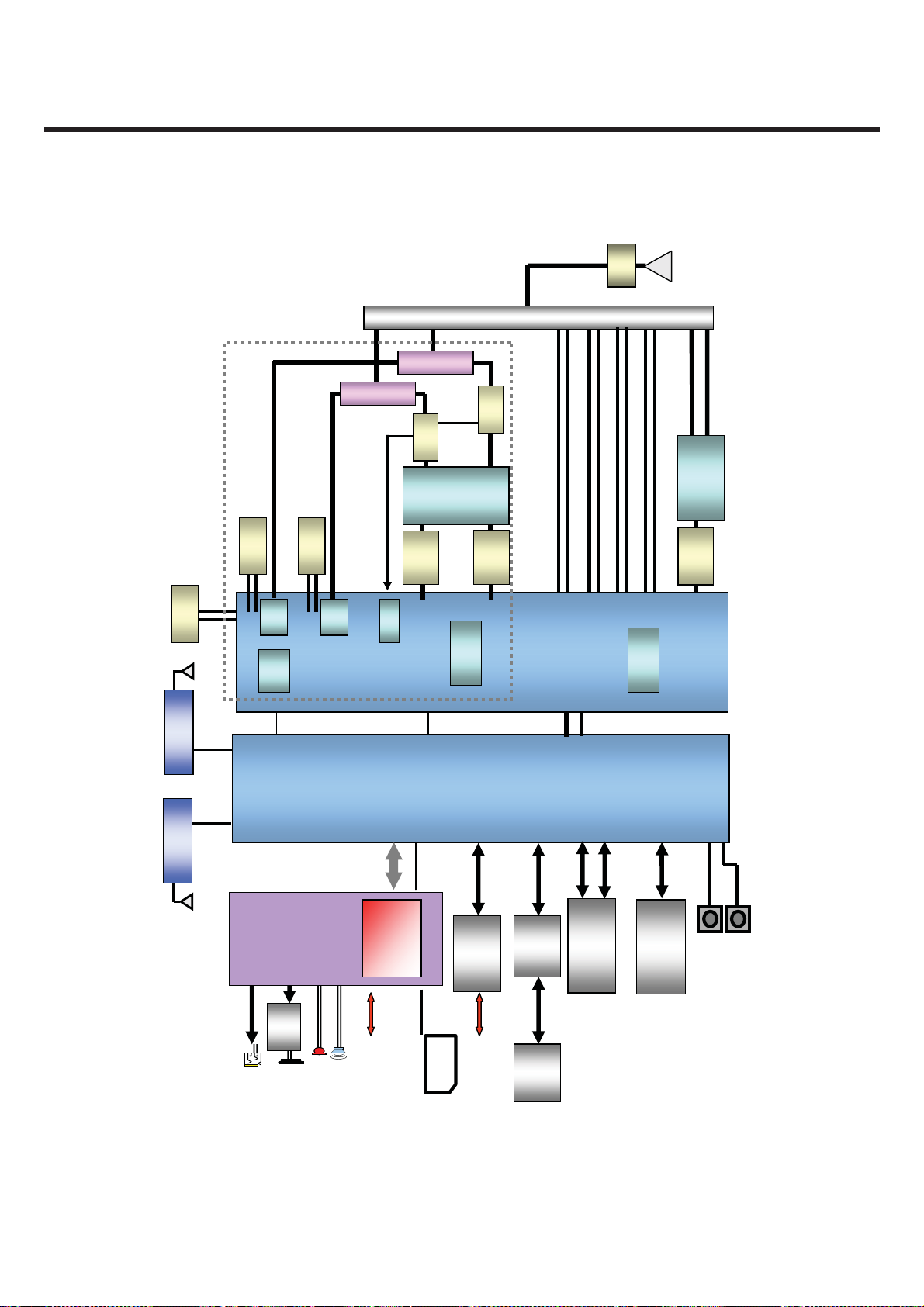
3.1 Digital Baseband(DBB) & Multimedia Processor
3.1.1 General Description
• Access subsystem
- Access Central Processing Unit (CPU) subsystem – ARM926, Joint Test Action Group (JTAG),
Embedded Trace Module (ETM), Instruction and Data (I&D)-cache, and I&D-TCM
- Access peripheral subsystems – Subscriber Identity Module (SIM) interface, IrDA®, Universal Serial
Bus (USB), Universal Asynchronous Receiver/Transmitter (UART), and so on
- Digital Signal Processor (DSP) subsystem – CEVA-X1620, JTAG, Static Random Access Memory
(SRAM), and Program Data Read Only Memory (PDROM)
- EDGE/GSM/GPRS (EGG) subsystem – EGG hardware accelerators
- WCDMA subsystem – WCDMA hardware accelerators
• Application subsystem
- Application CPU subsystem – containing ARM926, JTAG, ETM, I&D-cache, and I&D-TCM
- Application peripheral subsystems – I2C™, keypad, UART, and so on
- Graphics subsystem – XGAM subsystem
- Audio Processing Execution (APEX) and video encoder subsystems
In addition to the two subsystems above, there is also a test block, chip control block, and
a pad multiplexing block residing at the top level
y DSP
- The Digital Signal Processor Subsystem (DSPSUB) includes a DSP megacell, which
contains the DSP CPU together with a tightly coupled memory. The DSP is the Ceva-X
1620 core with a 64 kB instruction RAM and a 64 kB data RAM. It also contains debug
logic and interfaces. In addition to the megacell, the DSPSUB includes external memories,
peripheral units, and interfaces. The DSP megacell is clocked at 208 MHz.
- The DSPSUB includes an AHB master and an AHB slave interface. The AHB master
provides a direct access to the Internal Random Access Memory (IRAM) in the EGG core
through the AHB. The AHB slave interface allows the CPU and the DMA to access in the
program and data RAM residing in the DSPSUB.
y WCDMA subsystem
- The digital baseband controller WCDMA subsystem incorporate a WCDMA modem
- An interface to the WCMDA together with memory control and an internal single port
RAM. The WCDMA subsystem has three AHB slave interfaces.
- The Ericsson DB 3150 also includes HSDPA class 6 functionality.
- The WCDMA subsystem is handled and provided by Ericsson.
y XGAM subsystem
- The XGAM subsystem is a graphics acceleration module that provides hardware
support in the creation of visual imagery and the transfer of this data to a display.
The XGAM also provides support for connecting a Camera module. The visual data
could be graphics, still images, or video.
- The XGAM subsystem is handled and provided by Ericsson.
y Operation and Services
- IC™ Interface
-SIM Interfaces
- General Purpose I/O (GPIO) Interface
- External Memory Interface that supports NAND, NOR, PSRAM, SDRAM,
- JTAG
-RTC
- ETM (in Prototype Package)
3. TECHNICAL BRIEF
Copyright © 2009 LG Electronics. Inc. All right reserved.
Only for training and service purposes
- 19 -
LGE Internal Use Only
3. TECHNICAL BRIEF
SPDT
FEM (SWPlexer + GSM_RX_SAW)
26MHz
X-Tal
A-GPS
Bluetooth
850
RX_SAW
1900
LNA
W-VCO
RX_SAW
LNA
I/Q
HDET
Duplexer
1900
Duplexer
Coupler
WCDMA
PAM
TX_SAW
RF3300
W-VCO
850
Coupler
TX_SAW
SSB
I
SSB
I
DB3200
GSM 1900 Rx
GSM 1800 Rx
GSM 900 Rx
GSM-VCO
SSB
I
GSM 850 Rx
PAM
TX_SAW
900
1800/1900
GSM
GSM Tx/Rx
WCDMA Tx/Rx
AB3100
Power
850/90
0
Stereo Headset
05
TPA62
USIM
MIC
+5V
Receiver
r
Transceive
USB
Shifter
SD
SDRAM 1G
Level
Micro
(2.8” WQVGA)
NAND 2G
LCD
2M
VGA
Figure 3-1-1 GR500R Block Diagram
LGE Internal Use Only Copyright © 2009 LG Electronics. Inc. All right reserved.
- 20 -
Only for training and service purposes
3. TECHNICAL BRIEF
3.1.2 External memory interface
RF calibration data, Audio parameters and battery calibration data etc are stored in flash memory
area.
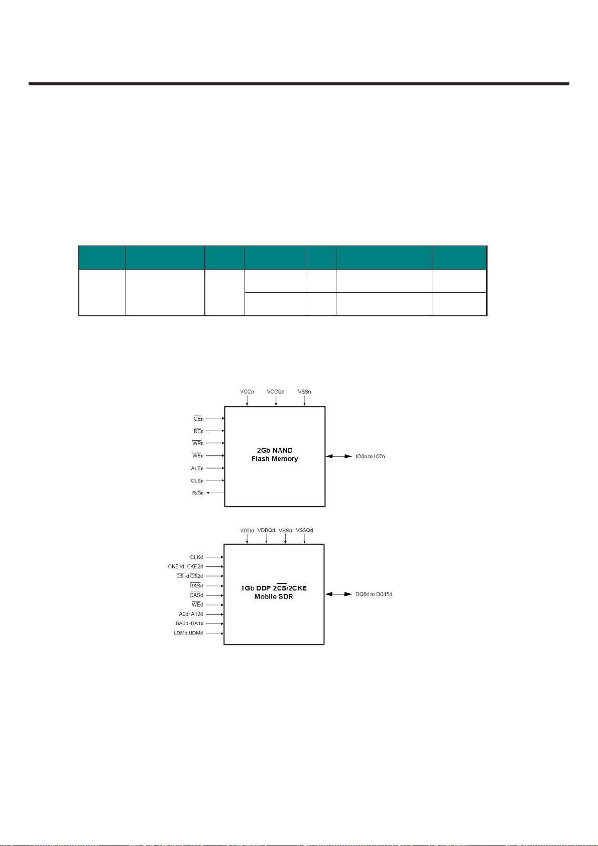
A. GR500R’s memory
y 2Gb NAND flash memory +1G SDRAM
Dev ic e Part Na me Mak e r Item Time Size Speed
Program speed 220μs 1Page=(2K + 64)Bytes 10.32MByte/s
NAND flash KA100J00BA-AJYY Samsung
Erase speed 1.5ms 1Block=(128K+4K)Bytes 88MBy te/s
Table 3- 1- 1. External Memory Interface Spec. of GR500
Figure 3- 1- 2. External Memory Configuration of GR500
y Package
- 10.5 by 13 mm 107 balls, 0.8mm pitch FBGA Production Package
Copyright © 2009 LG Electronics. Inc. All right reserved.
Only for training and service purposes
- 21 -
LGE Internal Use Only
3. TECHNICAL BRIEF
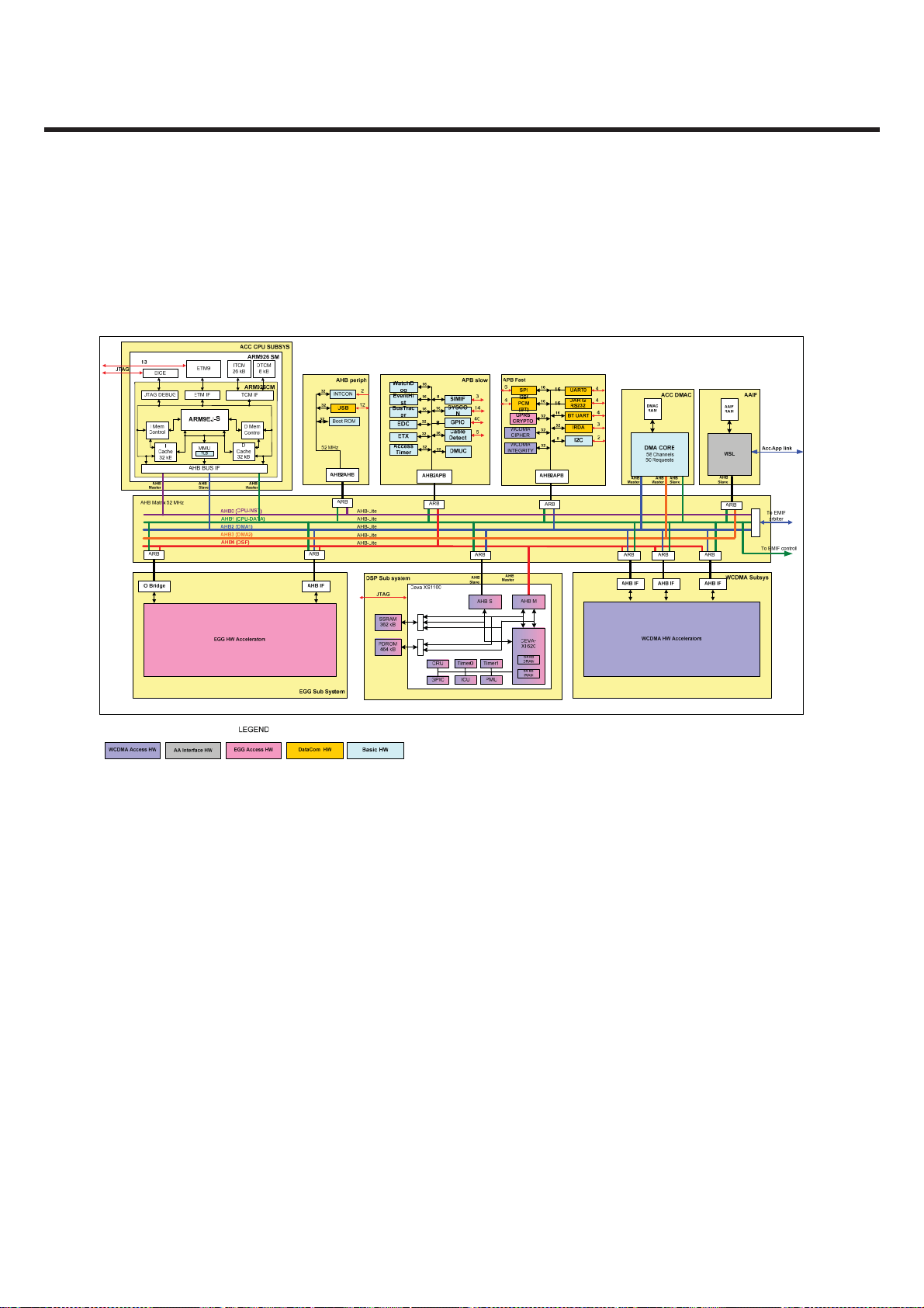
3.1.3 Hardware Architecture
A. Block Diagram
26
26
MHz
MHz
ARB
Figure 1 Access Architecture
Figure 3-1-3. Access system of Ericsson DB3200
LGE Internal Use Only Copyright © 2009 LG Electronics. Inc. All right reserved.
- 22 -
Only for training and service purposes
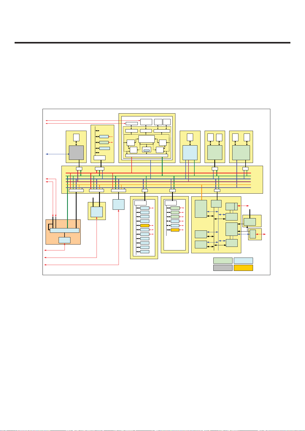
3.1.3 Hardware Architecture
A. Block Diagram
ETM
JTAG
32
Periferals
ISP
2
32
AHB Periph
INTCON
8
32
MS PRO
32
Boot ROM
52 MHz
32
EMIF
AHB2AHB
AHB
Slave
ARB
AHB
EMIF
AHB
AHB
Slave
Slave
SDRAM IF
Acc-App link
From Access system
SDRAM/NOR
55
SDRAM/NOR
55
55
PSRAM/NOR/NAND
AHB
Slave
AHB
Slave
EMIF Arbiter
SDRAM IF
AAIF
AAIF
RAM
Intel
MSL
AHB
Slave
ARB
ARB ARB
SEMIF
AHB
Slave
AHB
Slave
NOR/
PSRAM/
NAND IF
3. TECHNICAL BRIEF
APP CPU SUBSYS
ARM926 SM
DTCM
ITCM
ETM9
EICE
I Mem
Control
AHB
Cache
32 kB
I
AHB
Slave
AHB2APB
13 MHz
16
32
32
32
32
16
16
16
32
32
(Slow)
32
ETM IF
ARM9EJ-S
MMU
TLB
AHB BUS IF
AHB
Slave
ARB
APB SLOW
SYSCON
WDOG
TIMER0
TIMER1
UART0
KEYPAD
GPIO
RTC
BUS TR
Event H
DMUC
JTAG DEBUG
Master
ARB
52 MHz
4
11
24
8 kB
Cache
32 kB
Master
TCM IF
D
AHB
8 kB
ARM926CM
D Mem
Control
AHB
Slave
26 MHz
ARB
AHB2APB
(Fast)
32
16
16
2
3
32
16
MMC/SD
I2S/PCM0
I2S/PCM1
I2C0
I2C1
SPI
AHB
Master
APB FAST
8
4
4
2
2
6
APP DMAC
AAIF
RAM
DMA CORE
40 Channels
& Requests
AHB
Slave
AHB
Master
GRAM
64k byte
GAMEACC
MCiDCT
(Video)
APEX+
APEX
APEX
RAM
ROM
APEX
AHB
Slave
ARB
ARB
AHB
Slave
GAMCON
DATA
(3D)
CPU
MM HW
AA Interface HW
PDI
PDICON
CDI
CDICON
V ENC
RAM0
Video Encoder
AHB
Master
XGAM
PAR/ SSI
Data Com HW
Video Encoder
V ENC
RAM0
AHB
Slave
ARB
PDI
AHB
Slave
CamISP
Basic HW
APP BUS
AHB0 (Inst)
AHB1 (Data)
AHB2 (DMA0)
AHB3 (DMA1)
AHB4 (GAM)
AHB5 (V Enc)
AHB
Periferals
CDS
ISP
CDS
CDI
Figure 2 Application Architecture
Figure 3-1-4. Application system of Ericsson DB3200
Copyright © 2009 LG Electronics. Inc. All right reserved.
Only for training and service purposes
- 23 -
LGE Internal Use Only

3. TECHNICAL BRIEF
B. CPU Subsystem
- Access CPU subsystem
The digital baseband controller includes an access CPU subsystem, which includes the submodules
described below.
• 32 KiB I-cache
• 16 KiB D-cache
• Page table
• Memory Management Unit (MMU)
•JTAG
•ETM9
• 26 KiB I-TCM
•8 KiBD-TCM
- Application CPU subsystem
The digital baseband controller includes an Application CPU subsystem, which includes the
submodules described below.
• 32 KiB I-cache
• 16 KiB D-cache
• Page table
• MMU
•JTAG
•ETM9
•8 KiBI-TCM
•8 KiBD-TCM
C. Peripheral Hardware Subsystem
The digital baseband controller includes hardware that supports mobile terminal peripherals
such as a MMC, SD, UART, I2C, USB, keypad, and infrared. Collectively, this hardware
comprises the Peripheral subsystem.
The functional blocks of the Peripheral subsystem connect to the peripheral bus through four
separate bridges, which provide a simple interface to support different timing and memory
access arrangements.
D. DSP Hardware Subsystem
The Digital Signal Processor Subsystem (DSPSUB) includes a DSP megacell, which contains the DSP
CPU together with a tightly coupled memory. The DSP is the Ceva-X 1620 core with a 64 kB
instruction RAM and a 64 kB data RAM. It also contains debug logic and interfaces. In addition to the
megacell, the DSPSUB includes external memories, peripheral units, and interfaces. The DSP
megacell is clocked at 208 MHz.
The DSPSUB includes an AHB master and an AHB slave interface. The AHB master provides a direct
access to the Internal Random Access Memory (IRAM) in the EGG core through the AHB. The AHB
slave interface allows the CPU and the DMA to access in the program and data RAM residing in the
DSPSUB.
E. XGAM Subsystem
The XGAM subsystem is a graphics acceleration module that provides hardware support in the
creation of visual imagery and the transfer of this data to a display. The XGAM also provides support
for connecting a Camera module. The visual data could be graphics, still images, or video.
The XGAM subsystem is handled and provided by Ericsson.
LGE Internal Use Only Copyright © 2009 LG Electronics. Inc. All right reserved.
- 24 -
Only for training and service purposes
3. TECHNICAL BRIEF
F. System Control Subsystem
The SYSCON resides at the top level of the circuit architecture and is responsible for clock
generation and clock and reset distribution within the digital baseband controller, as well as to
external devices.
The block is a slave peripheral under control of the ARM processor. The programming of the
SYSCON controls the fundamental modes of operation within the digital baseband controller.
Individual blocks can also be reset and their clocks held inactive by accessing the appropriate
control registers.
3.1.4 RF Interface
A. DB3200 Interface
DB3200 controls GSM RF part using these signals through GSM RF chip-RF3300.
y RF_DATA_A
y RF_DATA_B
y RF_DATA_C
y TX_ADC_STRB
TX_ADC_STRB
RF_DATA_STRB
Figure 3-1- 5. Schematic of DB3200 RF Interface
B. WCDMA Radio Link Interface
y RF_WCDMA_PA_0_EN
y RF_WCDMA_PA_1_EN
y RF_WCDMA_DCDC_EN
y RF_WCDMA_PWRDET_E
RF_WCDMA_PA_0_EN
RF_WCDMA_PA_1_EN
RF_WCDMA_DCDC_EN
RF_WCDMA_PWRDET_E
Figure 3-1-6. Schematic of WCDMA RF Interface
RF_DATA_A
RF_DATA_B
RF_DATA_C
B15
B16
C15
D15
A16
B14
D14
B13
C13
QDATA_AMP_MSB
IDATA_FREQ_MSB
AMP_FREQ_LSB
TX_ADC_STRB
DATA_STR
WTX_BAND_2_EN
WTX_BAND_5_EN
WPOW_DET_EN
Copyright © 2009 LG Electronics. Inc. All right reserved.
Only for training and service purposes
- 25 -
LGE Internal Use Only
3. TECHNICAL BRIEF
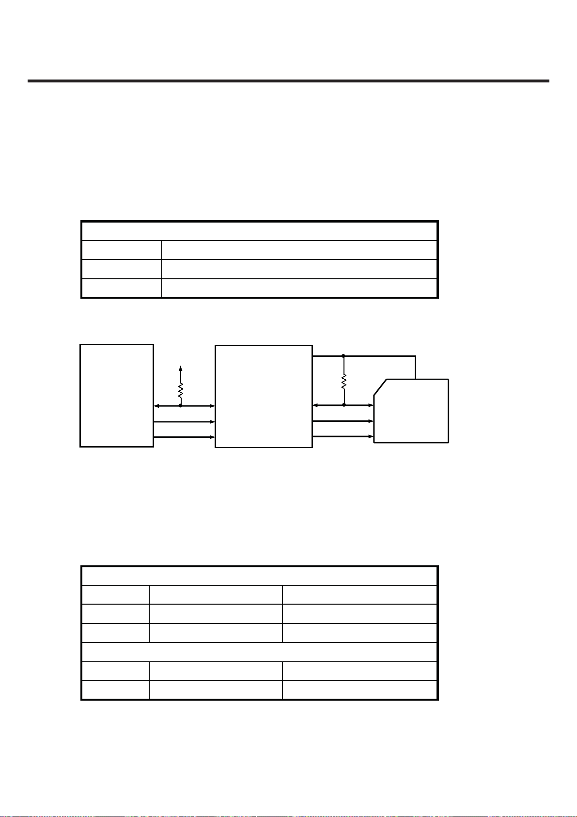
3.1.5 SIM Interface
SIM interface scheme is shown in Figure3-1-6.
SIMDAT0, SIMCLK0, SIMRST0 ports are used to communicate DB3200 with
AB3100 and filter.
SIM (Interface between DBB and ABB)
SIM card bidirectional data lineSIMDAT0
SIM card reference clockSIMCLK0
SIM card async/sync resetSIMRST0
Table 3-1-2. SIM Interface
DB3200
SIMDAT0
SIMCLK0
SIMRST0
VDDE
AB3100
10K
SDAT SIMDAT
SCLK SIMCLK
SRST SIMRST
Figure 3-1-7. SIM Interface
SIMVCC
3.1.6 UART Interface
UART signals are connected to DB3200 GPIO through IO connector
UART0
NoteNameResource
ACC Receive DataACC_UART0_RXACC_GPIO_2
ACC Transmit DataACC_UART0_TXACC_GPIO_3
10K
VDD
DAT
CLK CARD
RST
UART1
APP Receive DataAPP_UART_RXAPP_GPIO_0
APP Transmit DataAPP_UART_TXAPP_GPIO_1
Table 3-1-3. UART Interface
LGE Internal Use Only Copyright © 2009 LG Electronics. Inc. All right reserved.
- 26 -
Only for training and service purposes
3. TECHNICAL BRIEF
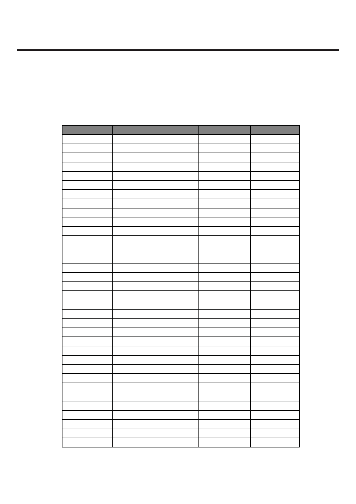
3.1.7 GPIO (General Purpose Input/Output) map
Total GPIO is composed of ACCESS part and APPLICATION part. ACCESS part has 39 allowable
resources and APPLICATION part has 31. GPIO Map, describing application, I/O state, and enable
level are shown in below table.
Initial StateI/ONameGPIO
LowOutputACC_USB_HS_STP00
LowOutputACC_USB_HS_DIR01
LowInputACC_UART0_RX02
LowOutputACC_UART0_TX03
LowInputACC_USB_HS_IN_CLK04
LowInputACC_USB_HS_NXT05
LowInputACC_USB_HS_DATA406
LowInputACC_USB_HS_DATA507
InputACC_USB_HS_DATA608
Low
LowInputACC_USB_HS_DATA709
LowInputACC_UART3_RX10
LowOutputACC_UART3_TX11
LowInputACC_UART3_CTS12
LowOutputACC_UART3_RTS13
LowInputN.C.14
LowOutputACC_GP_SUBLED_ON15
LowOutputACC_GP_USB_CS16
LowOutputACC_GPS_START17
LowInputACC_USB_HS_DATA318
LowInputACC_GP_FLIPSENSE19
LowInputACC_SPI_DI20
LowOutputACC_SPI_DO21
LowOutputACC_SPI_OUT_CLK22
LowInputN.C.23
LowInputACC_GP_LCD_ID24
LowInputN.C25
HighOutputACC_GP_SPI_BT_CSn26
LowInputACC_GP_SPI_BT_IRQ27
LowInputN.C28
LowInputN.C29
LowInputN.C30
LowInputN.C.31
LowInputN.C.32
LowInputN.C.33
Table 3-1-4. DB3200 ACC GPIO Map Table
Copyright © 2009 LG Electronics. Inc. All right reserved.
Only for training and service purposes
- 27 -
LGE Internal Use Only
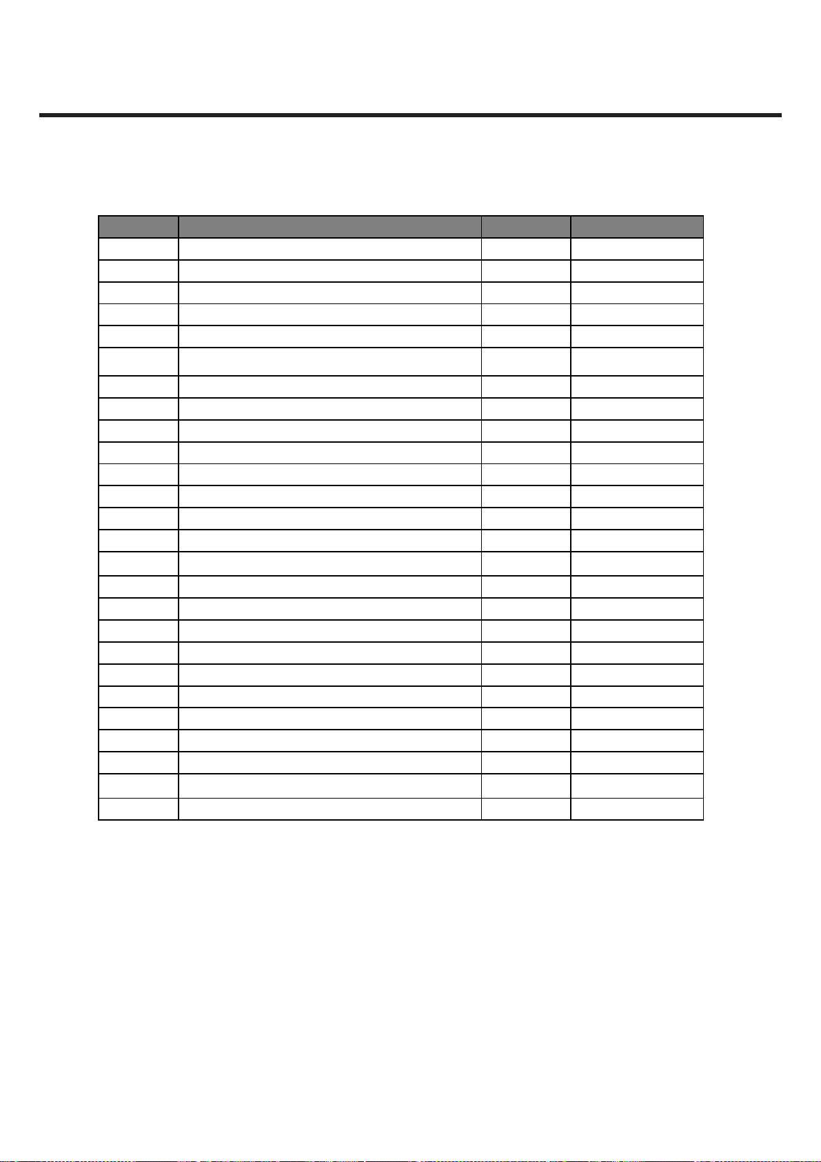
3. TECHNICAL BRIEF
Initial StateI/ONameGPIO
InputAPP_UART_RX00
Low
LowOutputAPP_UART_TX01
LowOutputAPP_GP_CAMLDO_EN02
LowInput/OutputAPP_GP_USW_SDA03
LowOutputAPP_GP_2M_SDN04
LowOutputAPP_GP_USW_SCL05
LowInput/OutputAPP_GP_TOUCH_SDA06
LowOutputAPP_GP_TOUCH_SCL07
HighInputAPP_GP_TOUCH_PENIRQn08
LowOutputAPP_GP_FLASHLED_EN09
LowOutputAPP_GP_FLASHLED_TORCH10
LowInputAPP_MMC_FB_CLK11
LowInputAPP_GP_MMC_DET12
LowInputAPP_GP_USW_INT13
LowInput/OutputAPP_GP_3AXIS_SDA14
LowOutputDCON (Dedicated)15
LowOutputAPP_GP_3AXIS_SCL16
LowInputAPP_GP_3AXIS_INT17
HighOutputAPP_GP_KEYENCODE_RST18
LowInput/OutputAPP_GP_KEYENCODE_SDA19
LowOutputAPP_GP_KEYENCODE_SCL20
LowInputAPP_GP_KEYENCODE_INT21
LowOutputAPP_GP_GPS_PON22
LowOutputAPP_GP_VGA_SDN23
LowOutputAPP_GP_MOTORLDO_EN24
LowOutputAPP_GP_LCDBL_CTRL25
Table 3-1-5. DB3200 APP GPIO Map Table
LGE Internal Use Only Copyright © 2009 LG Electronics. Inc. All right reserved.
- 28 -
Only for training and service purposes
3. TECHNICAL BRIEF
3.1.8 USB
The USB block supports the implementation of a “High-speed" device fully compliant to USB 2.0
standard. It provides an interface between the CPU (embedded local host) and the USB wire, and
handles USB transactions with minimal CPU intervention.
The USB specification allows up to 15 pairs of endpoints. Data for each endpoint is buffered in
RAM within the USB block and is read/written from the endpoint FIFO using DMA transfers or FIFO
register access. High-speed (high throughput) endpoints can use DMA while slower endpoints can
use FIFO register access.
The USB block can request up to six DMA channels, three for IN endpoints and three for OUT
endpoints.
NoteUSB Function
ULPI stop signalUSB_STP
ULPI direction signalUSB_DIR
USB clockUSB_CLK
ULPI next signalUSB_NXT
USB data0USB_DAT0
USB data1USB_DAT1
USB data2USB_DAT2
USB data3USB_DAT3
USB data4USB_DAT4
USB data5USB_DAT5
USB data6USB_DAT6
USB data7USB_DAT7
USB chip selectUSB_CS_PD
Power supply for DB3200 USB blockVBUS
Table 3-1-6. USB Signal Interface of DB3200
Copyright © 2009 LG Electronics. Inc. All right reserved.
Only for training and service purposes
- 29 -
LGE Internal Use Only
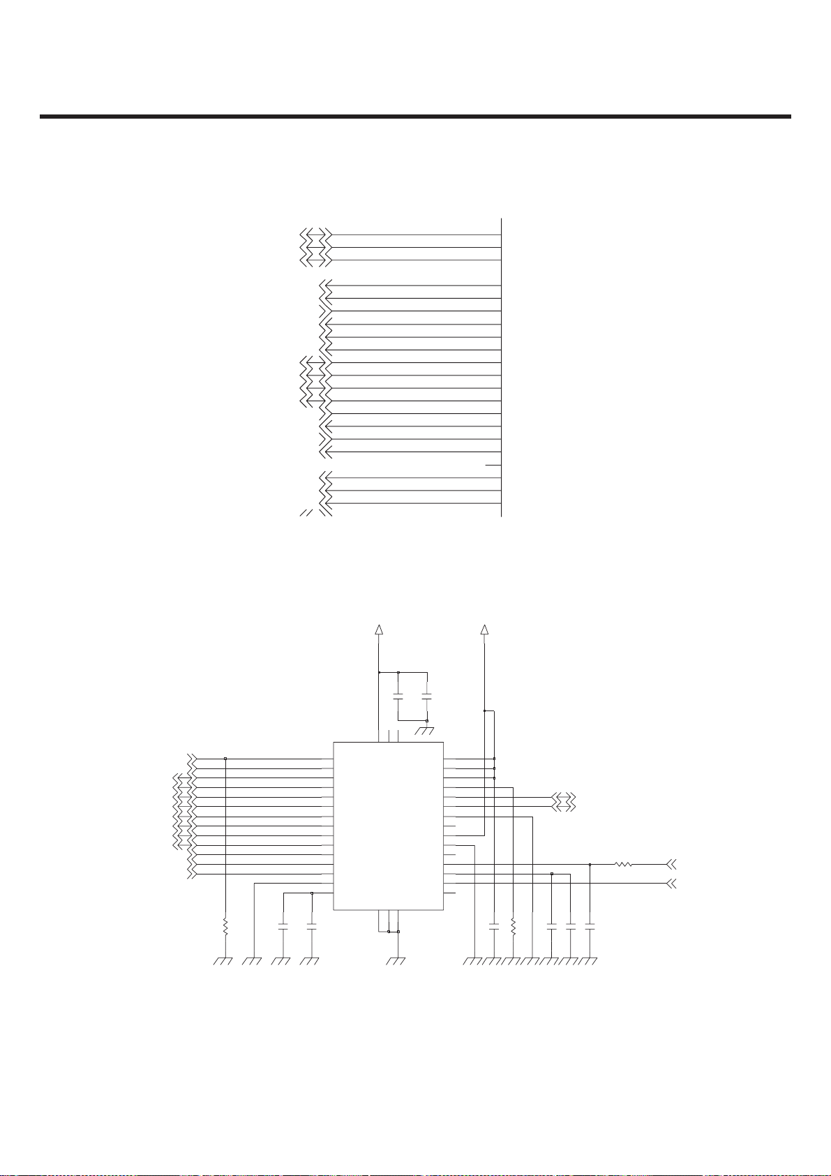
3. TECHNICAL BRIEF
A
CA
C
C
A
2
J
S
U
0ATAD_B
1ATAD_BSU
_
U
S
C
A
C
A
C
CA
2ATAD
B
S_S
PT
_BSU_
H
R
ID_SH_BSU_CC
0TRAU_CCA
XR_
CA
C
_BSU_CCA
T_0
X
TRAU_
K
S
LC_NI_
H
TXN_SH_BSU_
A
4AT
_SH_BSU_CCA
D
5ATAD_SH_BSU_CC
AT
S
SU_C
B
H_
CA
P
_
G
CA
6
_
AD
A
7AT
_SH_BSU_CCA
D
R_3TR
X
AU_C
3T
XT_
AU_CCA
R
A
_CCA
U
_CCA
U
_
US
G
_CCA
TC_3TR
A
S
T
R
R
S
_3T
LB
O_DE
N
S
SU_P
_B
C
ATS_SPG_C
TR
U
K
2
3L
U
J
3
A
K
3
L
8
A
CC
1G
A
C
K
8
C
A
F
1
A
8J
C
A
3G
CA
H
3
G
2
CA
H
9
A
1
E
1
0
H
D
1
A
F
3
A
C
C
4D
CCA
3C
A
C
C
5
G
E
4
MV_0ES_BS
PV_TAD_BSU
EO_BS
P
_OI
0
G_CC
_OIPG_CCA
1
_
2_OIPG
IP
3_O
_C
G
P
_OI
4
G_C
5_OIPG_CC
6
_OIPG_C
7_OIPG_C
P
8_OI
_CCA
G
9
_OIPG_C
01_OIPG_CC
IP
1_O
_CCA
1
G
P
_CCA
_OI
G
21
3
1
G_CC
_OIP
41_OIPG
_
51_OIPG_
PBSU_
61_OIPG
R
_
B
71_OIPG_CCA
Table 3-1-8. Schematic of DB3200 USB block
V
0.1uC607
8V1_EDD
M
D_BSU
U
PD_BS
12K
1%
R604
0.1uC608
106R
K1
C609 4.7u
C610 2.2u
SUBV
1
ATX_BSU
L
A
BV
T
006
C
6C
0
F3
F2
3
C
C
U_PG_C
CA
C
BSU_C
A
U
BS
S
B
U
_CCA
C
A
A
A
SH_BSU_
C
U_CCA
C
C
A
U_CC
A
SC_BS
KL
C_N
I_SH_
0ATA
D_BSU
ATAD
1
_
AT
2
D_
A
3
TAD_SH_BSU
A
D_
4AT
A
TAD_SH_BS
5A
6
TAD_SH_BSU_C
A
D_SH_BSU_C
7ATA
T
SU_CCA
XN_SH_B
PTS_SH_BSU_CC
D
R
_SH_B
I
S
306R
K15
5
C
06
06C
6
.0
u1
7.4
u
S_PIH
4
A
KCOLC
B
1
ATAD
0
1
A
A
1
D
TA
2
A
2ATAD
A
3
3ATAD
5A
4
D
ATA
6A
A
TA
5
D
6B
A
D
6AT
6
C
7
D
ATA
D
5
T
XN
D
6
PT
S
5E
R
ID
1
E
F
G
0
C
E
6
R
V1FE
NC1
NC2
LE
VCC
U
6
10
8
GND1
GND2
GND3
E4
D2
10
.
u1
u7
.4
V
01
F1
4C
T
E
TS
5B
1OI_C
CV
2
B
2OI_CCV
2
C
FERR
1C
M
D
1
D
D
P
E
TEA8051PSI
C5
2
L
T
F
UA
3
D
D
I
3B
C
2GF
4B
1GF
C
4
D
P
N_WS
4
F
SUB
V
3E
R
V3GE
3
5F
1LATX
6
F
2
X
LAT
Table 3-1-9. Schematic of USB Transceiver
LGE Internal Use Only Copyright © 2009 LG Electronics. Inc. All right reserved.
- 30 -
Only for training and service purposes
3. TECHNICAL BRIEF
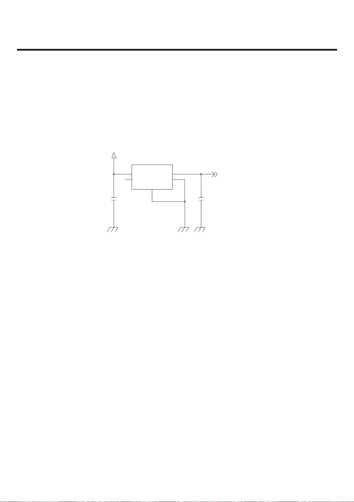
3.1.9 Slider ON/OFF Detection
There is a magnet to detect the slide module status, up or down.
If a magnet is close to the hall-effect switch U604, the voltage at Pin 1 of U604 goes to 0V. Otherwise
1.8V.
This SLIDE_DET signal is delivered to DB3200 ACC_GP_FLIPSENSE.
8V1_EDDV
4
U
6
0
025U
B
13
XVN
4
DV
D
C
N
6C
02
u
1.0
DI
LS
E
PGND
D
1
TUO
23
DNG
5
E
T
Figure 3-1-9. Slider On/Off Detector
_PG_CC
A
126
C
0
u1.
ES
NESPILF
TCE
Copyright © 2009 LG Electronics. Inc. All right reserved.
Only for training and service purposes
- 31 -
LGE Internal Use Only
 Loading...