

Page 1

COLOR MONIT OR
SER VICE MANUAL
CHASSIS NO. : CL-18
MODEL: FPD1570, LB680A
CAUTION
BEFORE SERVICING THE UNIT,
READ THE SAFETY PRECAUTIONS IN THIS MANUAL.
Page 2
CONTENTS
SPECIFICATIONS
1. LCD CHARACTERISTICS
Type : TFT Color LCD Module
Size : 335.0(H) x 273.5(V) x 11.2(D)
Pixel Pitch : 0.243mm x 0.243mm
Color Depth : 8-bit, 16,777,216 colors
Active Video Area : 15.7inch (39.88cm)
(39.832diagnal 311mm x 284.8mm)
Surface Treatment : Anti-Glare, Hard Coating (3H)
Backlight Unit : Two-CCFL (Cold Cathode
Fluorescent Lamp)
2. OPTICAL CHARACTERISTICS
2-1. Viewing Angle by Contrast Ratio
≥
10
Left : 60° typ., 60° min.
Right : 60° typ., 60° min.
Top : 45° typ., 45° min.
Bottom : 45° typ., 45° min.
2-2. Luminance : 200 cd/m
2
typ.
2-3. Angle at Half Luminance
Left : 45° min.
Right : 45° min.
Top : 45° min.
Bottom : 45° min.
2-4. Contrast Ratio : 250 typ.
3. SIGNAL (Refer to the Timing Chart)
3-1. Sync Signal
1) Type : Separate Sync. (Horizontal & Vertical)
2) Input Voltage Level: Low=0~0.8V, High=2.1~5.5V
3) Sync Polarity : Positive or Negative
3-2. Video Input Signal
1) Type : R, G, B Analog
2) Voltage Level : 0~0.714 V
a) Color 0, 0 : 0 Vp-p
b) Color 7, 0 : 0.467 Vp-p
c) Color 15, 0 : 0.714 Vp-p
3) Input Impedance : 75 Ω
3-3. Operating Frequency
Horizontal : 30 ~ 80kHz
Vertical : 56 ~ 85Hz
4. POWER SUPPLY
4-1. Power Adaptor
Input : AC 100~240V, 50/60Hz 1.2A
Output : DC 24V 1.2A
4-2. Power Consumption
5. ENVIRONMENT
5-1. Operating Temperature: 10°C~35°C (50°F~95°F)
(Ambient)
5-2. Relative Humidity : 10%~80%
(Non-condensing)
5-3. Altitude : 0~10,000ft (3,030m)
6. DIMENSIONS (with TILT/SWIVEL)
Width : 370.2mm (14.57'')
Depth : 134.0mm (5.27'')
Height : 387.7mm (15.26'')
7. WEIGHT (with TILT/SWIVEL)
Net. Weight : 4.5kg (9.92 lbs)
Gross Weight : 6.8kg (14.99 lbs)
SPECIFICATIONS ................................................... 2
PRECAUTIONS ....................................................... 3
TIMING CHART ....................................................... 4
OPERATING INSTRUCTIONS ................................ 5
CONTROL LOCATIONS ......................................... 8
WIRING DIAGRAM ................................................. 8
DISASSEMBLY ....................................................... 9
BLOCK DIAGRAM ................................................. 11
DESCRIPTION OF BLOCK DIAGRAM.............. 12
ADJUSTMENT ...................................................... 13
TROUBLESHOOTING GUIDE .............................. 14
PRINTED CIRCUIT BOARD................................... 20
EXPLODED VIEW...................................................22
REPLACEMENT PARTS LIST ...............................24
PIN CONFIGURATION............................................31
SCHEMATIC DIAGRAM......................................... 36
MODE
POWER ON (NORMAL)
STAND-BY
SUSPEND
DPM OFF
POWER OFF
H/V SYNC
ON/ON
OFF/ON
ON/OFF
OFF/OFF
-
POWER CONSUMPTION
less than 36 W
less than 3 W
less than 3 W
less than 3 W
less than 3 W
LED COLOR
GREEN
AMBER
AMBER
AMBER
OFF
VIDEO
ACTIVE
OFF
OFF
OFF
-
-
+
Page 3
- 3 -
WARNING FOR THE SAFETY-RELATED COMPONENT.
• There are some special components used in LCD
monitor that are important for safety. These parts are
marked on the schematic diagram and the
replacement parts list. It is essential that these critical
parts should be replaced with the manufacturer’s
specified parts to prevent electric shock, fire or other
hazard.
• Do not modify original design without obtaining written
permission from Gate Way. or you will void the original
parts and labor guarantee.
TAKE CARE DURING HANDLING THE LCD MODULE
WITH BACKLIGHT UNIT.
• Must mount the module using mounting holes arranged
in four corners.
• Do not press on the panel, edge of the frame strongly
or electric shock as this will result in damage to the
screen.
• Do not scratch or press on the panel with any sharp
objects, such as pencil or pen as this may result in
damage to the panel.
• Protect the module from the ESD as it may damage the
electronic circuit (C-MOS).
• Make certain that treatment person’s body are
grounded through wrist band.
• Do not leave the module in high temperature and in
areas of high humidity for a long time.
• The module not be exposed to the direct sunlight.
• Avoid contact with water as it may a short circuit within
the module.
• If the surface of panel become dirty, please wipe it off
with a softmaterial. (Cleaning with a dirty or rough cloth
may damage the panel.)
WARNING
BE CAREFUL ELECTRIC SHOCK !
• If you want to replace with the new backlight (CCFL) or
inverter circuit, must disconnect the AC adapter
because high voltage appears at inverter circuit about
650Vrms.
• Handle with care wires or connectors of the inverter
circuit. If the wires are pressed cause short and may
burn or take fire.
PRECAUTION
CAUTION
Please use only a plastic screwdriver to protect yourself
from shock hazard during service operation.
CAUTION
• There is two backlight, must distinguish between
the top (upper) and the bottom (lower), and be
careful of treatment it.
• MTBF (Mean Time Between Failure) of a backlight
is about 25,000 hours.
Top (Upper) Backlight Ass’y
(P/N: 6913TZZ003A)
Bottom (Lower) Backlight Ass’y
(P/N: 6913TZZ003B)
IF BRIGHTNESS OF THE LCD MODULE DARKEN,
REPLACE THE BACKLIGHT ONE OR ALL.
Page 4
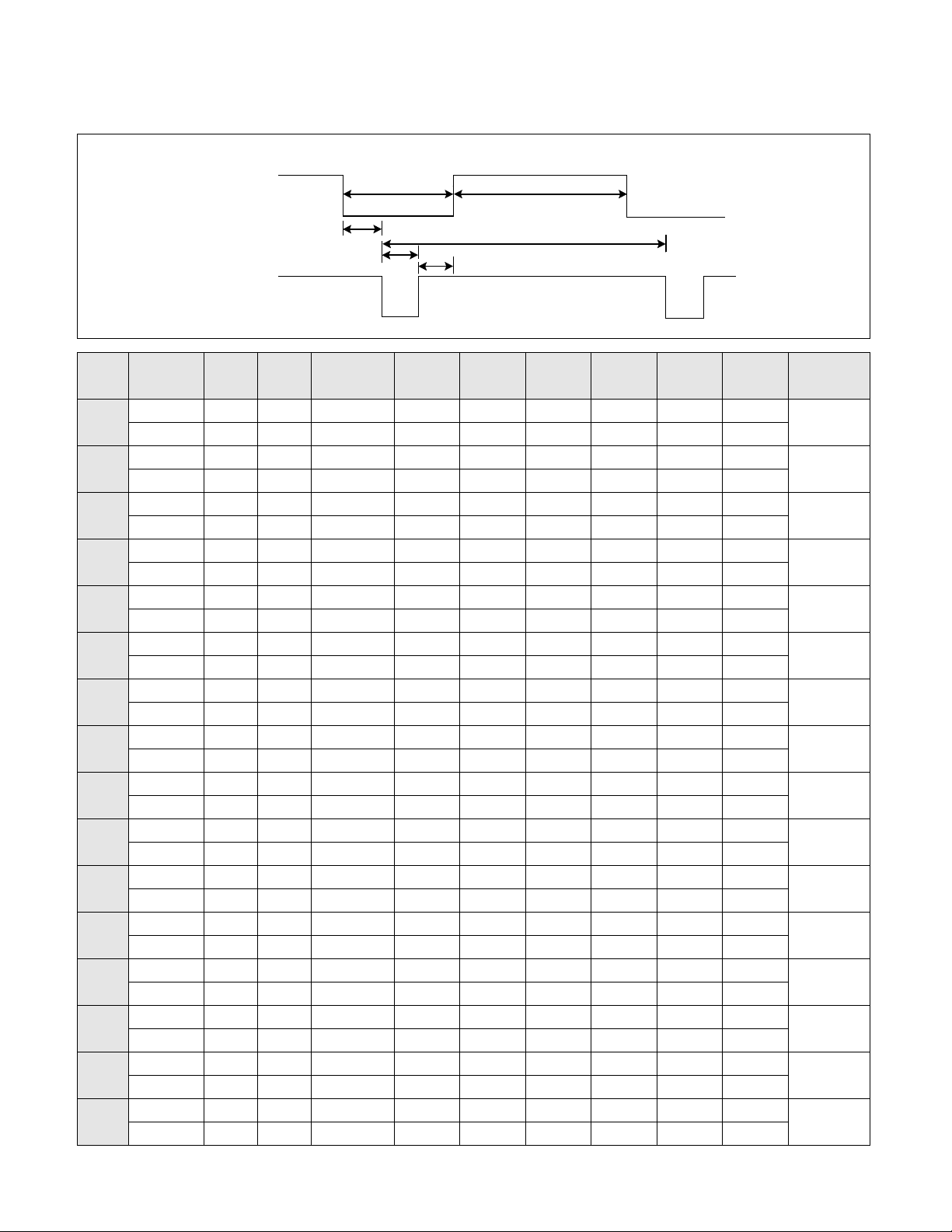
TIMING CHART
- 4 -
VIDEO
SYNC
B
D
C
F
E
A
H / V
H (Pixels)
V (Lines)
H (Pixels)
V (Lines)
H (Pixels)
V (Lines)
H (Pixels)
V (Lines)
H (Pixels)
V (Lines)
H (Pixels)
V (Lines)
H (Pixels)
V (Lines)
H (Pixels)
V (Lines)
H (Pixels)
V (Lines)
H (Pixels)
V (Lines)
H (Pixels)
V (Lines)
H (Pixels)
V (Lines)
H (Pixels)
V (Lines)
H (Pixels)
V (Lines)
H (Pixels)
V (Lines)
H (Pixels)
V (Lines)
Sync
Polarity
+
–
–
+
–
–
–
–
–
–
+
+
+
+
+
+
+/–
+/–
–
–
–
–
+
+
+/–
+/–
+/–
+/–
+
+
+
+
Dot
Clock
25.175
28.321
25.175
31.5
36.0
40.0
49.5
56.25
57.283
65.0
78.75
94.5
100.0
92.978
108.0
135.0
Frequency
31.469 KHz
70.8 Hz
31.468 KHz
70.8 Hz
31.469 KHz
59.94 Hz
37.5 KHz
75 Hz
43.269 KHz
85.0 Hz
37.879 KHz
60.317 Hz
46.875 KHz
75.0 Hz
53.674 KHz
85.061 Hz
49.725 KHz
74.55 Hz
48.363 KHz
60.0 Hz
60.123 KHz
75.029 Hz
68.677 KHz
84.997 Hz
68.681 KHz
75.062 Hz
61.805 KHz
65.96 Hz
63.981 KHz
60.02 Hz
79.976 KHz
75.035 Hz
Resolution
640 x 350
720 x 400
640 x 480
640 x 480
640 x 480
800 x 600
800 x 600
800 x 600
832 x 624
1024 x 768
1024 x 768
1024 x 768
1152 x 870
1152 x 900
1280 x 1024
1280 x 1024
Total
Period
( E )
800
449
900
449
800
525
840
500
832
509
1056
628
1056
625
1048
631
1152
667
1344
806
1312
800
1376
808
1456
915
1504
937
1688
1066
1688
1066
Video
Active
Time ( A )
640
350
720
400
640
480
640
480
640
480
800
600
800
600
800
600
832
624
1024
768
1024
768
1024
768
1152
870
1152
900
1280
1024
1280
1024
Blanking
Time
( B )
160
99
180
49
160
45
200
20
192
29
256
28
256
25
248
31
320
43
320
38
288
32
352
40
304
45
352
37
308
42
408
42
Sync
Duration
( D )
96
2
108
2
96
2
64
3
56
3
128
4
80
3
64
3
64
3
136
6
96
3
96
3
128
3
134
4
12
3
144
3
Back
Porch
( F )
48
59
54
35
48
33
120
16
80
25
88
23
160
21
152
27
224
39
160
29
176
28
208
36
144
39
200
31
248
38
248
38
Front
Porch
( C )
16
38
18
12
16
10
16
1
56
1
40
1
16
1
32
1
32
1
24
3
16
1
48
1
32
3
18
2
48
1
16
1
MODE
1
2
3
4
5
6
7
8
9
10
11
12
13
14
15
16
Page 5
OPERATING INSTRUCTIONS
FRONT VIEW REAR VIEW
Front Control Panel
1. Power ON/OFF Button
Use this button to turn the monitor on or off.
2. Power Indicator
This indicator lights up green when the monitor
operates normally; in DPMS (Energy Saving) mode,
-stand-by, suspend, or power off mode -its color
changes to orange.
3. Button
Use these buttons to choose or adjust items in the on screen
display.
4
AUTO/SET Button
Use this button to enter a selection in the on screen display.
5. OSD Button
Use this button to enter or exit the on screen display.
Buttons
OSD Button
AUTO/SET Button
Power Button
Power Indicator
DC Power Connecter
-
+
D-Sub Signal
Connector
15 4
3
2
100
100
<Shortcut Keys>
• Brightness and Contrast can be adjusted directly
without entering the On Screen Display (OSD)
system. Touch the buttons to adjust the
settings and then the OSD button to save all
changes. The Brightness and Contrast functions are
also available in the On Screen Display (OSD) menu.
* AUTO adjustment function
Touch the AUTO/SET button before using OSD menu.
This button is for the automatic adjustment of the
screen position, clock and phase.
Note: Some signal from some graphics boards may
not function properly. If the results are
unsatisfactory, adjust your monitor’s Position, Clock
and Phase manually.
PROCESSING
AUTO CONFIGURATION
Page 6
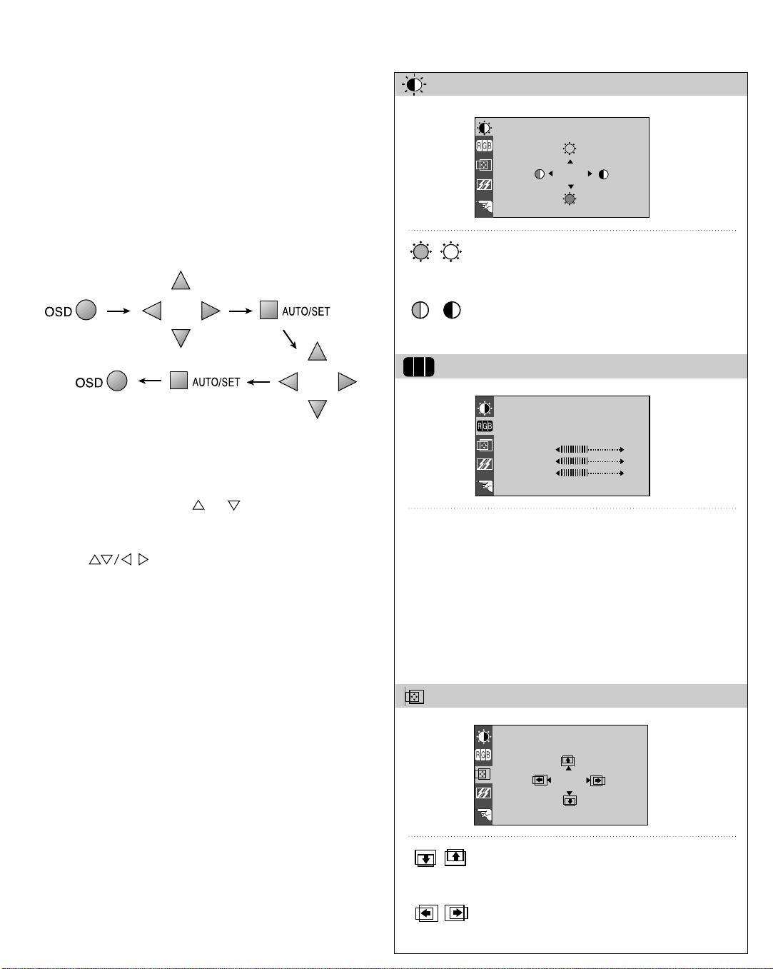
On-Screen-Display (OSD) Control
88
100
BRIGHTNESS CONTRAST
9300K 6500K
COLOR
PRESET
RED
GREEN
BLUE
RGB
61
39
POSITION
To adjust an image size, position, and operating
parameters are quick and easy with the On-ScreenDisplay control system, using the OSD button and the
Adjustment control button. A quick example is given below
to familiarize you with use of the controls.
Example;
Note:
Allow the monitor to stabilize for at least 30 minutes
before making image adjustment.
To make adjustments in the On Screen Display, follow these
steps:
Listed below are icons, icon names, and icon descriptions
of the OSD menu.
BRIGHTNESS CONTRAST
Brightness
Used to adjust the brightness of the
screen.
Contrast
Adjust the display to the contrast
desired.
COLOR
1. Press the OSD Button, then the main menu of the OSD
appears.
2.
To acces a control, use the or Buttons. When the icon
you want becomes highlighted, press the AUTO/SET Button.
3.
Use the Buttons to adjust the item to the desired
level.
4.
Accept the changes by pressing the AUTO/SET Button.
5.
Exit the OSD by Pressing the OSD Button.
PRESET
RED
GREEN
BLUE
POSITION
9300K/ 6500K
To appear the displays color
temperature.
• 9300K:Slightly bluish white.
• 6500K:Slightly reddish white.
To set your own color levels.
To set your own color levels.
To set your own color levels.
Vertical Position
To move image up and down.
Horizontal Position
To move picture image left and right.
Page 7
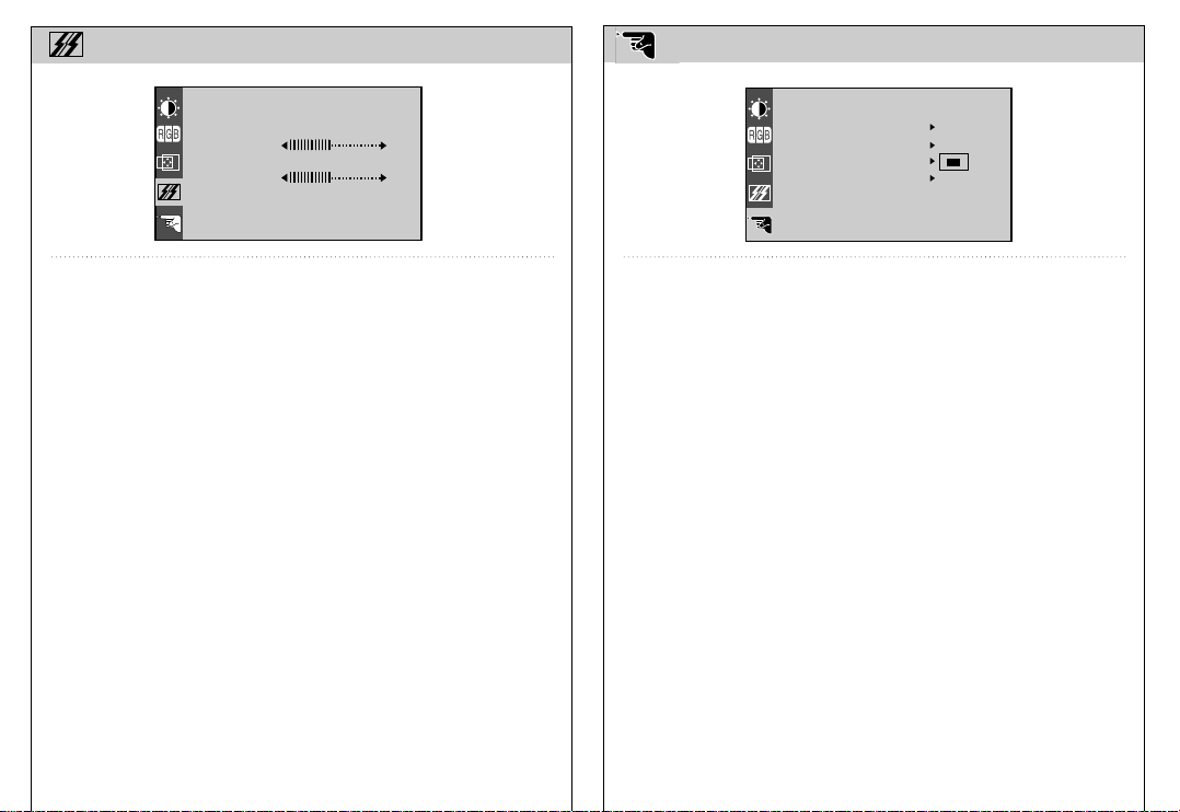
TRACKING
TRACKING
CLOCK
PHASE
LANGUAGE ENGLISH
FULL
OSD POSITION
48.3kHz / 60.0Hz
PRESET MODE
MODE INFO ON
IMAGE SIZE
SETUP
SETUP
CLOCK
PHASE
To minimize any vertical bars or
stripes visible on the screen
background.The horizontal screen
size will also change.
To adjust the focus of the display.
This item allows you to remove any
horizontal noise and clear or
sharpen the image of characters.
LANGUAGE
To choose the language in which the
control names are displayed.
IMAGE SIZE
This function displays the image in its
original size or enlarged size so as to
fit in the full screen of the LCD panel.
OSD POSITION
To adjust position of the OSD
window on the screen.
MODE INFO
There is information of video modespreset and user modes.
Page 8
CONTROL LOCATIONS
CN3
J10
J4
J2
CN2
CN1
J301
MAIN PCB
CONTROL PCB
12 5
67
3
4
WIRING DIAGRAM
NO.
1
2
3
4
5
6
7
Ref. No.
SW301
SW304
SW303
SW306
SW302
SW307
SW305
Control Function
OSD BUTTON
ADJUST LEFT
ADJUST UP
ADJUST DOWN
ADJUST RIGHT
AUTO/SET
POWER SWITCH
Page 9
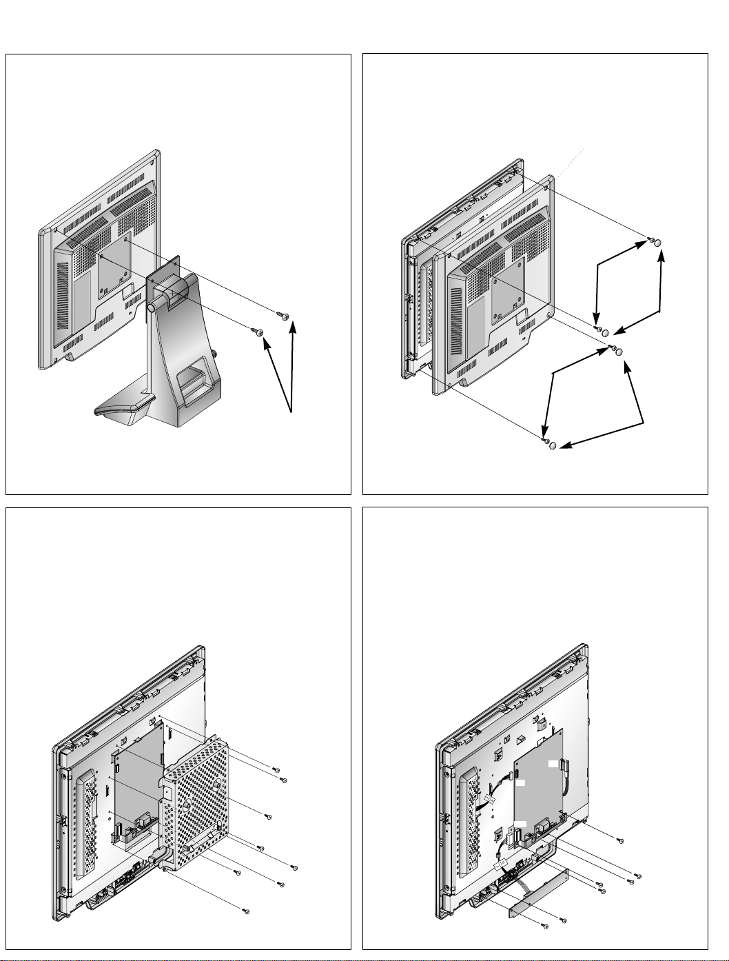
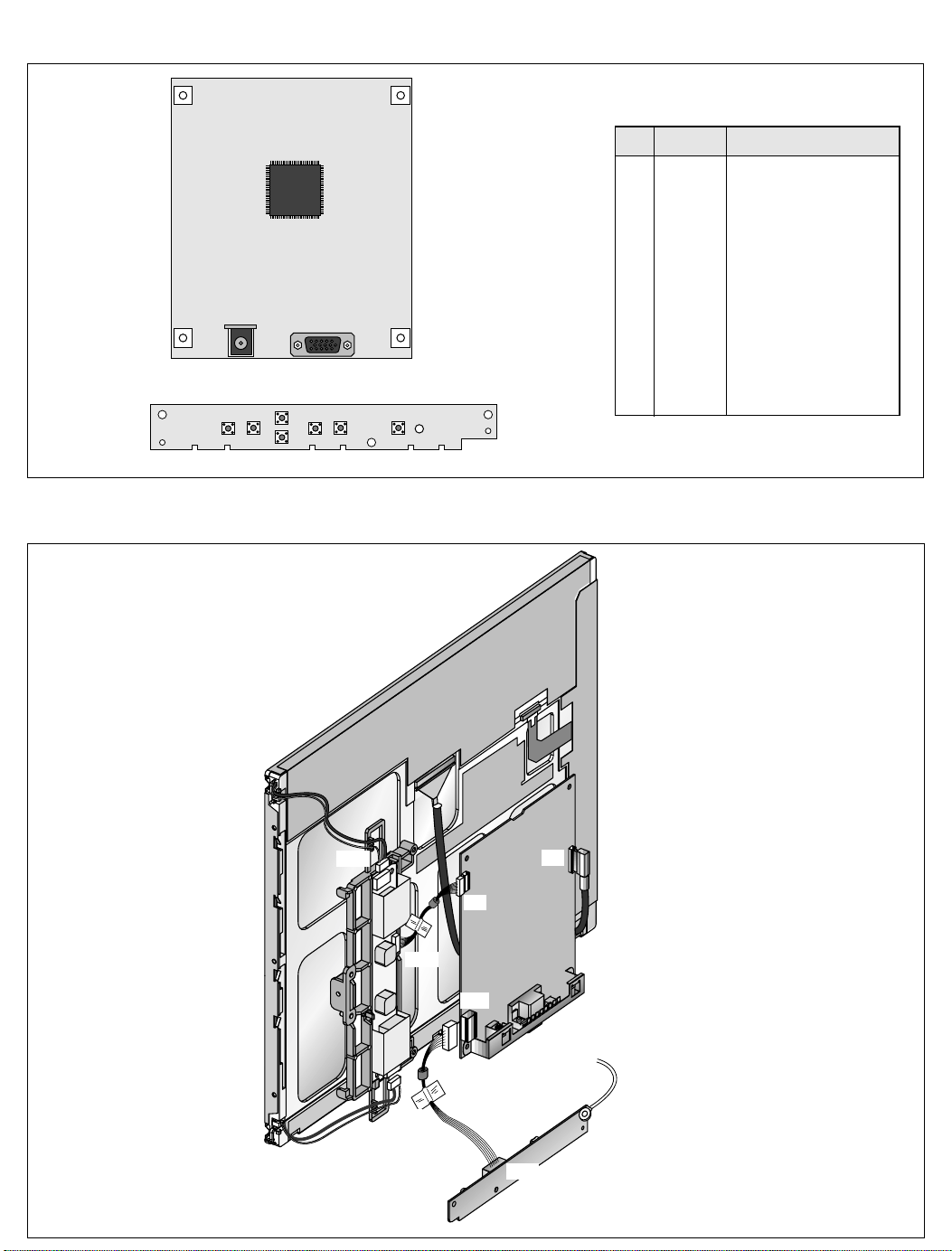
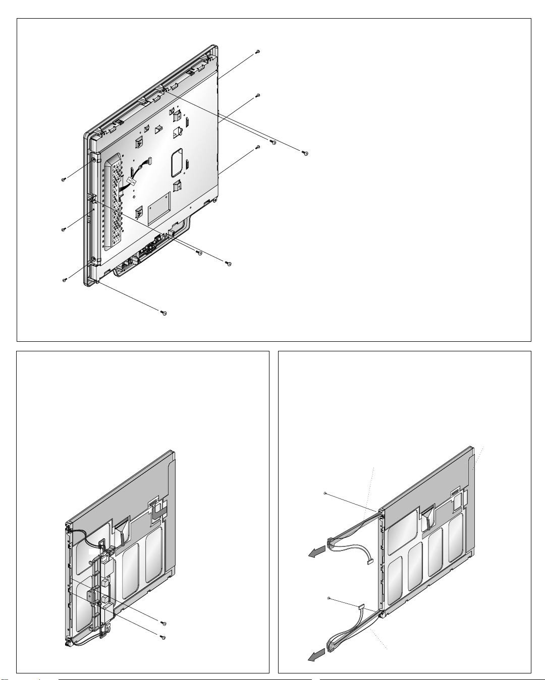
DISASSEMBLY
(a)
(a)
(a)
(a)
(a)
(a)
(a)
(a)
1. TILT/SWIVEL REMOVAL
(1) Remove two screws (a).
(2) Remove the Tilt/swivel.
(a)
2. BACK COVER REMOVAL
(1) Remove four sheet (a) from Back Cover.
(2) Remove four screws (b) from the Back Cover.
(3) Remove the Back Cover.
Back Cover
(b)
(a)
(b)
(a)
3. METAL REAR ASSEMBLY REMOVAL
(1) Remove eight screws (a).
(2) Remove the Metal rear Ass’y.
4. CONTROL, MAIN PCB ASSEMBLY
REMOVAL
(1) Disconnect J2, J4 and J10.
(2) Remove four screws (a).
(3) Remove the Main PCB Ass’y.
(4) Remove three screws (b).
(5) Remove the Control PCB Ass’y.
J2
J4
J10
(b)
(b)
(a)
(b)
(a)
(a)
(a)
Page 10
(b)
(b)
(b)
(b)
(b)
(a)
5.METAL FRAME ASSEMBLY
REMOVAL
(1) Remove five screws (a).
(2) Remove six screws (b).
(a)
(3)Remove theMetal Frame Ass’y
(b)
5. INVERYTER REMOVAL
(1) Disconnect CN2,CN3 .
(1) Remove two screws (a).
(2) Remove the Inverter.
CN3
(a)
(a)
(a)
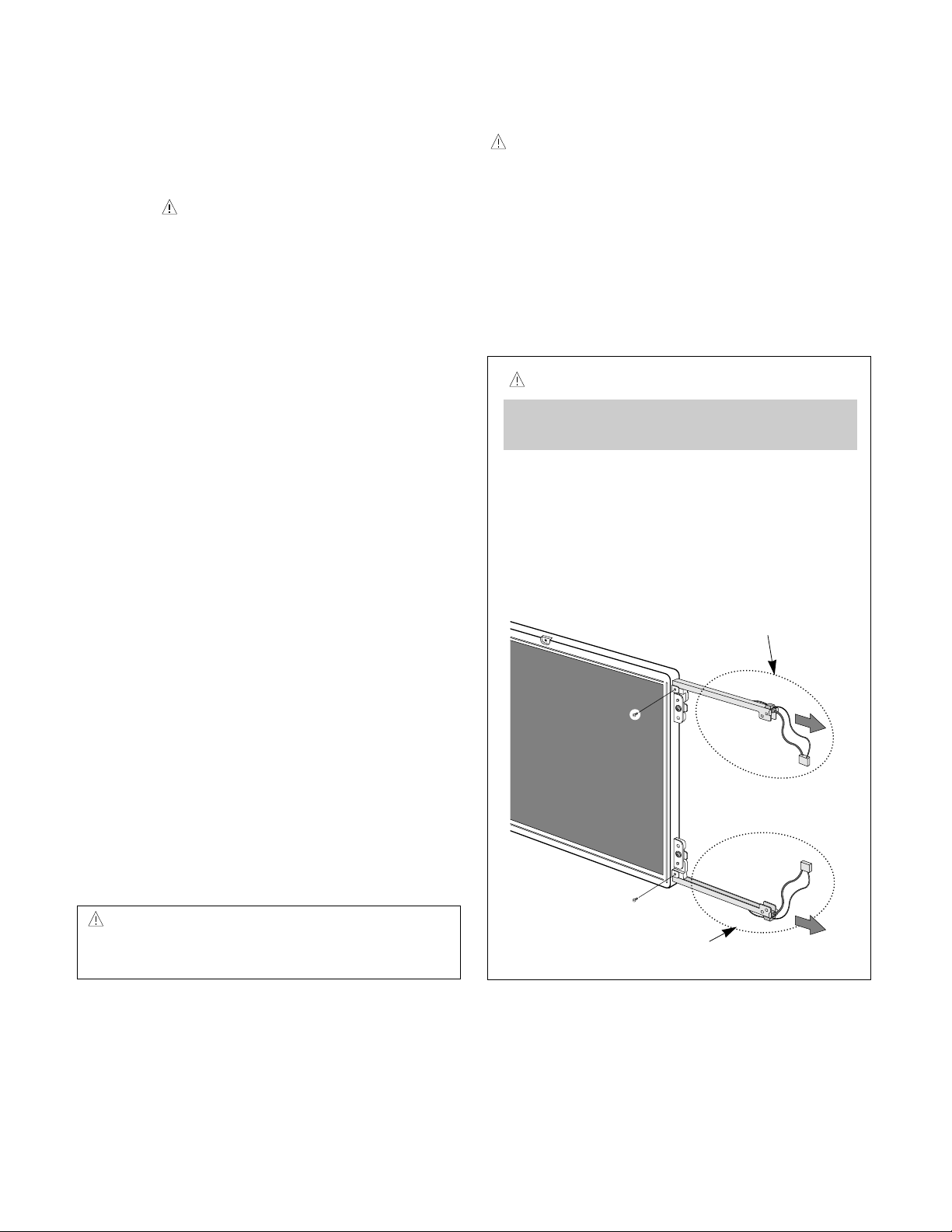
6. BACKLIGHT REMOVAL
(1) Remove two screws (a).
(2) Remove the Backlight from the LCD Module.
LCD Module
Top (Upper) Backlight Ass’y
(a)
CN2
(a)
(a)
(a)
Bottom (Lower) Backlight Ass’y
Page 11
D-SUB
Video Controller
MX88L282
LVDS
(LVDS83)
LVDS
(LVDS83)
Memory
(KM416S102BT)
H-Sync
A/D
converter
AD9884
M-CLK
Out - CLK
DE ,H/V Sync out
R,G,B odd
Out - CLK
DE ,H/V Sync out
R,G,B Even
LCD Module
R,G,B
differential
L VDS:Low Voltage Differential Signaling
Data 48 BitAddress
H-Sync
R,G,B
3.3V
3.3V
3.3V
ADC CLK
ADC CLK
R,G,B
even, odd
Micom
68HC08-BD48
Inverter CTL
Module CTL
V-Sync
Power CTL
H-Sync
3.3V
Inverter
24V
DC-DC
Converter
3.3V
Reg.
3.3V
24V Input
5.0V
5.0V
Video Signal
3.3V
3.3V
Page 12

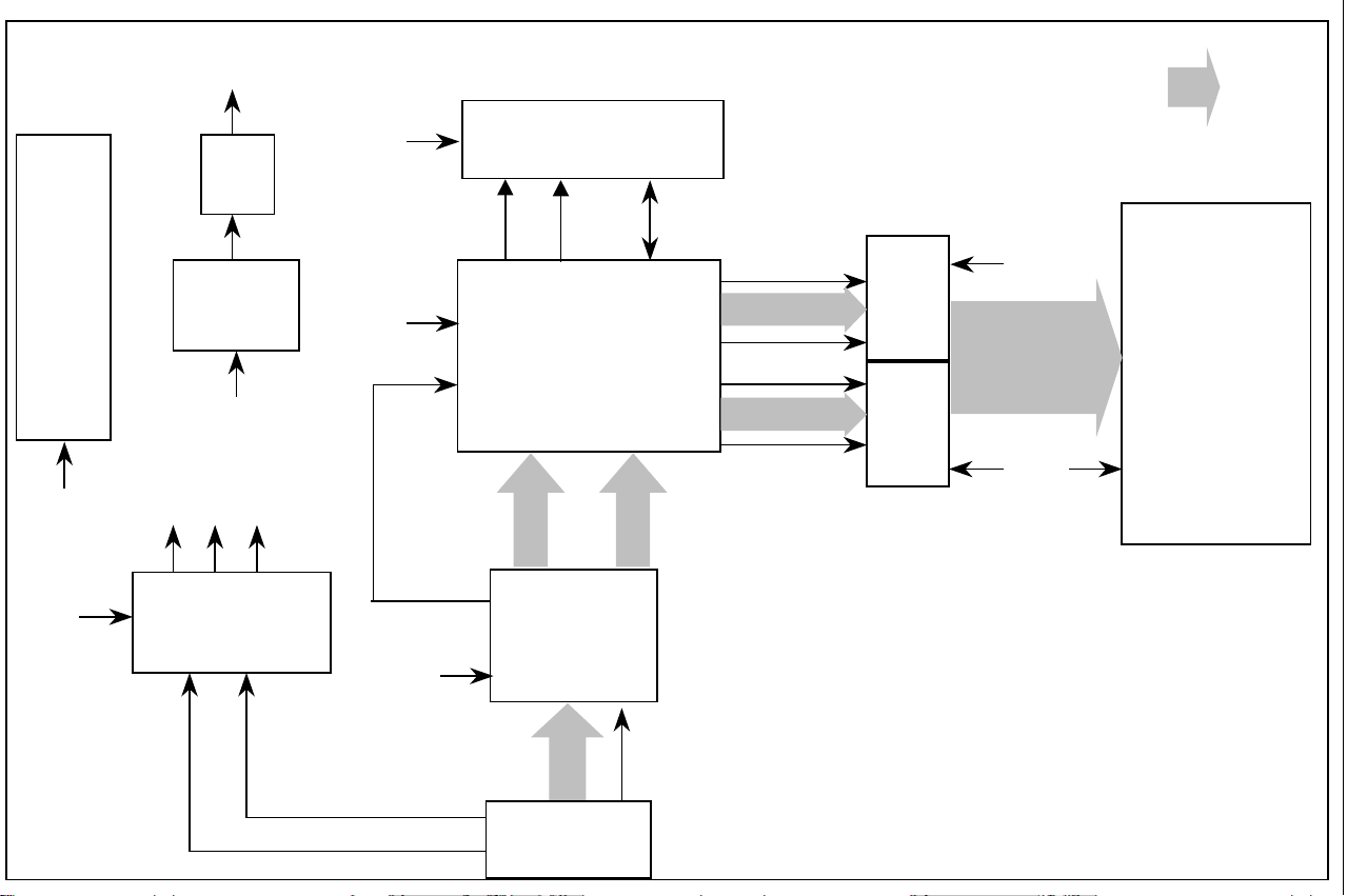
DESCRIPTION OF BLOCK DIAGRAM
- 12 -
1. Pre-amp/ ADC / PLL Part.
This part amplifies the level of video signal for the digital conversion and converts from the analog video signal to the
digital video signal using a pixel clock.
The pixel clock for each mode is generated by the PLL.
The range of the pixel clock is from 25MHz to 135MHz.
2. Video Controller Part.
This part consists of the Scaler and frame buffers which converts frame rate of input signal to 60Hz frame rate.
The Scaler gets the video signal converted analog to digital, interpolates input to 1280 X 1024 resolution signal and
outputs 8-bit R, G, B signal to transmitter.
3. Display Data Transmitter Part.
This part transmit digital signal from the Scaler to the receiver of module.
4. Power Part.
This part consists of the DC/DC converter and several 3.3V regulators .
The DC/DC converter coverts 24V to be entered power adapter to 5V.
5V, output of DC/DC converter, supply to the micom and 3.3V regulators.
The output voltage of 3.3V regulator supply to IC of each part.
5. MICOM Part.
This part consists of EEPROM IC which stores control data, Reset IC and the Micom.
The Micom distinguishes polarity and frequency of the H/V sync are supplied from signal cable.
The controlled data of each mode is stored in EEPROM.
6. Inverter
The inverter converts from 24V to AC 700Vrms and drive back-light lamp of module.
Page 13
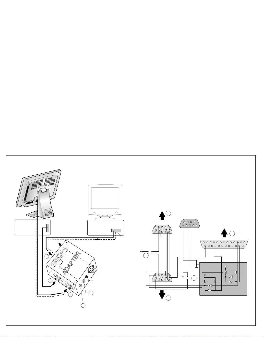
ADJUSTMENT
220
IBM
Compatible PC
PARALLEL PORT
Power inlet (required)
Power LED
ST Switch
Power Select Switch
(110V/220V)
Control Line
Not used
RS232C
PARALLEL
V-SYNC
POWER
ST
VGS
MONITOR
E
E
V-Sync On/Off Switch
(Switch must be ON.)
F
F
A
A
B
B
C
C
15
10
5
5
69
1
1
1
14
13
25
6
5V
5V
5V
4.7K
4.7K
4.7K
74LS06
74LS06
OFF ON
OFF
ON
11
All adjustment are thoroughly checked and corrected
when the monitor leaves the factory, but sometimes
several minor adjustment may be required.
Adjustment should be following procedure and after
warming up for a minimum of 10 minutes.
Alignment appliances and tools.
- IBM Compatible PC
- Programmable Signal Generator.
(eg. VG-819 made by Astrodesign Co.)
- E(E)PROM with each mode data saved.
- Alignment Adapter and Software.
1. Adjustment for Factory Preset Mode
1) Run alignment program for FPD1570 on the IBM
compatible PC.
2) Select EEPROM all clear command and Enter.
3) Display cross hatch pattern at Mode 1.
4) Select COMMAND PRESET START command.
5) Select FOS DEFAULT command and Enter.
6) Press "Y" key, it will automatically save all FOS data
to EEPROM.
2. Adjustment for White Balance
1) Display color 0,0 pattern at Mode 13.
2) Set External Bright to MAX position and Contrast to
MAX Position.
3) Select PRESET START
→ BIAS CAL command
and Enter.
4) No attempt to manually adjust, BIAS data is automatically adjusted and saved to the EEPROM.
5) Display color 15,0 pattern at Mode 13.
6) Select DRIVE CAL command and Enter.
7) Color 1 (9300K) and Color 2 (6500K) are
automatically adjusted and saved to the EEPROM.
8) Select PRESET EXIT command and Enter.
Figure 1. Cable Connection
Page 14

TROUBLESHOOTING GUIDE
NO POWER
(POWER INDICATOR OFF)
1. NO POWER
CHECK U15
INPUT VOLTAGE
(24V) ?
YES
CHECK
5VST VOLTAGE
(5V) ?
YES
CHECK
U4 PIN 6.
IS THIS PIN
OSCILLATED?
NO
NO
NO
TROUBLE IN
ADAPTOR or
INVERTER
TROUBLE IN
U15
TROUBLE IN
U4 or X2
YES
TROUBLE
SOMEWHERE ELSE
Page 15

NO RASTER
2. NO RASTER
CHECK
J4 PIN 10
(24V) ?
YES
CHECK
J4 PIN 5 (5V) ?
YES
CHECK
U4 PIN 42
H. PULSE ?
YES
CHECK
U5 PIN 117
H.PULSE?
YES
NO
NO
NO
NO
TROUBLE IN
POWER ADATER
TROUBLE IN
INON PATTERN
TROUBLE IN
U106, U105, U101,
U109
TROUBLE IN
U5
CHECK
U5 PIN 115
AD CLOCK ?
YES
NO
TROUBLE IN
U5
Page 16

YES
CHECK
U1 PIN 254
DOT CLOCK ?
YES
CHECK
MEMORYCLK
U6, U7, U8
PIN 35 ?
YES
CHECK
U1 PIN 93, 94
DOT CLOCK ?
YES
NO
NO
NO
CHECK
ADC-CLK PATTERN
TROUBLE IN
U1
TROUBLE IN
U1
CHECK
U1 PIN 124
D26 (H.PULSE) ?
YES
NO
TROUBLE IN
U1
Page 17

YES
CHECK
U2, U11 PIN 27
H.PULSE ?
YES
CHECK
U2, U11 PIN 28
V.PULSE ?
YES
CHECK
U2, U11 PIN 31
DOT CLOCK?
YES
CHECK
U2, U11 PIN 30
H.PULSE?
NO
NO
NO
NO
TROUBLE IN
U1
TROUBLE IN
U1
TROUBLE IN
U1
TROUBLE IN
U1
YES
TROUBLE IN
LCD MODULE
Page 18

NO DOT CLOCK
YES
3. NO CLOCK (CLOCK GENERATOR)
CHECK
U5Vcc
3.3V ?
CHECK
U5 PIN 115
CLOCK ?
YES
NO
NO
TROUBLE IN
U23
TROUBLE IN
U5
Page 19

TROUBLE IN DPM
CHECK
U617 (MICOM)
PIN 1, 42 (H/V INPUT)
SIGNAL ?
YES
4. TROUBLE IN DPM
NO
TROUBLE IN
U17
CHECK
U4 PIN 6
WAVEFORM
(24MHz) ?
YES
CHECK
U4 PIN 26
(5V) ?
YES
TROUBLE IN PC
NO
NO
TROUBLE IN
X2
TROUBLE IN
SIGNAL CABLE
Page 20

C66
C62
C47
R13
R20
J2
U23
U20
U19
U13
R12
C150
C209
C35
R15
C1
C49
R101
C65
C201
R104
U2
BA18
C151
C153
C152
U11
C175
C174
CA17
C50
BA36
R103
C193
C194
R100
C64
R64R63
L5
C235
L24
C234
L6
C99
J5
BA19
BA20 BA21 BA22 BA23 BA24 BA40 BA41
BA43BA42
BA45
BA44
X1
CA11
CA18
BA30
BA33
R76
C73
C74
60
50
D5
C3
R98
C198
C195
C63
R102
R62
C233
R66
R65
Model:LB680A Ver:1.3
U8
P/N:6870T285A10
Date:2000.09.20
BA7
120
110
100
90
70
R16
C15
CA12CA15
C13
BA27BA35
70
30
D4
D3
ZD2
ZD1
BA8
BA9
140
130
6050
CA16CA9
BA29RA32
90
80
20
U6
BA12
BA11
BA10
160 150
40
30
CA10CA13
BA26BA34
U5
100
51
10
BA14
BA13
BA15
170
2010
CA14
CA7
BA28
BA31
L3
120
110
C72
125
D1
D2
BA16
BA17
U1
1
CA8
BA25
C67
C96
R92
D6
J3
R94
U7
BA3
C101
C181
BA1
210
200
BA37BA38
230
220
BA39
C60
255
R24
U3
R91
C196
Q7Q3
R93
Q8
C197
C95
C184
BA5
BA4BA6
C190
C177
C42
ZD3
R37
R27R31
R26
R36
L1
U17
J1
C89
C48
C59
C127
U14
U10
R30
U9
L7
Q6
R52
R59
R32
R60
U24
U16
U12
C61
C31
R50
R49
R83
C56
C55
C32
X2
R84
Q2
R68
C36
Q5
R58
C37
L26
C57
C38
C40
Q4
C58
L9
U15
R80C30
R47
Q1
R48
L12
L13
C192
C135
J4
1
C41 L27
L23
C188
ZD6
U4
L4
J10
1. MAIN BOARD (Component Side)
Page 21

C186C51
C118
C204
R1
C24
C27
R14
C25
C230
C229
C53
C129
C128
C126
C21
C5
L2
C142
C143
L8
C103
C26
C166
C167
C168
C54
C52
C124C123
C133
C131
C130
C125
C136
C140
C137
C146
C145
C155
C156
C149
C154
C160
C169
C170
C173
C172
C171
C83
C94
C93
C92
R23
C110
C134
C122
C144
C139
C138
C147
C141
C23
C158
C157
C148
C163 C161
C164
C162
C165
C17
C85
R74
C88
C90
C91
C117C120
C114C116
C121
C16
C19
C14
C22
C20
C159
C18
C81
C79
R73C87
C86
C84
R18
R19
C11
C70
C77
C76
C78
C80
C82
R90
C111
C115
C112
C98
C97
C102
R8
R7
L10
C9
R17
R10
R11
C12
C68
C75
C69
C71
C203
R97
R96
C109
C108
C105
C104
C107
C106
C8
R4
C4
R9
C6
R6
C7
C10
R2
R67
R21
R78
C202
R110
C182
C180
C100
R3
R5
R130
R132
R56
R55
R53
R38
R135
R133
R45
R46
R61
C33
R109
R108
R89
R99
C224
R111
C39
R88
C113C183
R70
C119
C176
R54
R25
R77
R125
R42
R41
R43
R44
R126
R121
R28
C132
C231
C178
C179
C200
R86
R85
R82
R35
R87
R39
R40
C191
R29
R33
R34
R57
R51
R95
C2
C232
R22
C199
R81
R79
R75
R69
R72
C189
C187
C185
R124
C46
C45
C44
C43
C34
C29
C28
L17 L16
R71
2. MAIN BOARD (Solder Side)
Page 22

EXPLODED VIEW
1
2 3
4
5
A
8
9
10
10-1
13
12
7
6
EXPLODED VIEW PARTS LIST
Ref. No.
1
2
3
4
5
6
7
8
9
10
10-1
11
12
13
A
Part No.
3091TKL021C
6304TLT157A
6632Z-1502D
6871TST198A
4951TKS062A
6871TMT213A
6631T11010E
4951TKK044A
3809TKL016C
5410TKK020B
332-113F
3043TKK070B
332-105F
6634TBZ009E
3313TL5022A
Description
CABINET ASS’Y, LB680A G/WAY 3090TKL019A PC+ABS, 12446B
LCD , LGPHILIPS TFT LCD LM157E2-A2, 15.7” 1280x1024 W/O I
INVERTER, NMC1502 15.1”
PWB(PCB)ASS’Y, SUB LB680A XAGT BRAND CONTROL
METAL ASS’Y, FRAME LB680A
PWB(PCB)ASS’Y, MAIN LB680A XGWC G/WAY CL-18 TOTAL
CONNECTOR ASS’Y, 30P H-H 140MM UL-20276 LB680A
METAL ASS’Y, REAR LB680A
BACK COVER ASS’Y, LB680A 017A G-WAY, 12446B
INSULATION, PVC SHEET LB680
SCREW, PVP+3x12(MSWR/FZMY)
TILT SWIVEL ASS’Y, LG680, (G/WAY, 12446B)
SCREW, PVS+4x10(MSWR/FZMW)
ADAPTER, AC-DC, PSCV360107 SAMSUNG 100-240V 24V 1.5A FOR G/WAY
MAIN TOTAL ASS’Y, LB680A G/WAY CL-18
Page 23

REPLACEMENT PARTS LIST
CAUTION: BEFORE REPLACING ANY OF THESE COMPONENTS,
READ CAREFULLY THE SAFETY PRECAUTIONS IN THIS MANUAL.
* NOTE : S SAFETY Mark
AL ALTERNATIVE PARTS
MODEL: FPD1570 DATE: 2000. 10. 11.
*S *AL LOC. NO. PART NO. DESCRIPTION / SPECIFICATION REMARK
MAIN BOARD
CAPACITORs
C1 0CH8107F611 CAPACITOR, CHIP, [AL. ELECTROLYTIC], 100UF 16V M 85STD(CYL) R/TP
C2 0CH3104K566 CAPACITOR, CHIP, [CERAMIC LD-LESS HD], 0.1UF 50V K X 2012 R/TP
C3 0CH6150K416 CAPACITOR, CHIP, [CERAMIC LD-LESS TC], 15PF 50V J NP0 2012 R/TP
C4 0CH3104K566 CAPACITOR, CHIP, [CERAMIC LD-LESS HD], 0.1UF 50V K X 2012 R/TP
C5 0CH3104K566 CAPACITOR, CHIP, [CERAMIC LD-LESS HD], 0.1UF 50V K X 2012 R/TP
C6 0CH3104K566 CAPACITOR, CHIP, [CERAMIC LD-LESS HD], 0.1UF 50V K X 2012 R/TP
C7 0CH3104K566 CAPACITOR, CHIP, [CERAMIC LD-LESS HD], 0.1UF 50V K X 2012 R/TP
C8 0CH3104K566 CAPACITOR, CHIP, [CERAMIC LD-LESS HD], 0.1UF 50V K X 2012 R/TP
C9 0CH3104K566 CAPACITOR, CHIP, [CERAMIC LD-LESS HD], 0.1UF 50V K X 2012 R/TP
C10 0CH3104K566 CAPACITOR, CHIP, [CERAMIC LD-LESS HD], 0.1UF 50V K X 2012 R/TP
C11 0CH3104K566 CAPACITOR, CHIP, [CERAMIC LD-LESS HD], 0.1UF 50V K X 2012 R/TP
C12 0CH3104K566 CAPACITOR, CHIP, [CERAMIC LD-LESS HD], 0.1UF 50V K X 2012 R/TP
C13 0CH6150K416 CAPACITOR, CHIP, [CERAMIC LD-LESS TC], 15PF 50V J NP0 2012 R/TP
C14 0CH3104K566 CAPACITOR, CHIP, [CERAMIC LD-LESS HD], 0.1UF 50V K X 2012 R/TP
C15 0CH6150K416 CAPACITOR, CHIP, [CERAMIC LD-LESS TC], 15PF 50V J NP0 2012 R/TP
C16 0CH3104K566 CAPACITOR, CHIP, [CERAMIC LD-LESS HD], 0.1UF 50V K X 2012 R/TP
C17 0CH3104K566 CAPACITOR, CHIP, [CERAMIC LD-LESS HD], 0.1UF 50V K X 2012 R/TP
C18 0CH3104K566 CAPACITOR, CHIP, [CERAMIC LD-LESS HD], 0.1UF 50V K X 2012 R/TP
C19 0CH3104K566 CAPACITOR, CHIP, [CERAMIC LD-LESS HD], 0.1UF 50V K X 2012 R/TP
C20 0CH3104K566 CAPACITOR, CHIP, [CERAMIC LD-LESS HD], 0.1UF 50V K X 2012 R/TP
C21 0CH3104K566 CAPACITOR, CHIP, [CERAMIC LD-LESS HD], 0.1UF 50V K X 2012 R/TP
C22 0CH3104K566 CAPACITOR, CHIP, [CERAMIC LD-LESS HD], 0.1UF 50V K X 2012 R/TP
C23 0CH3104K566 CAPACITOR, CHIP, [CERAMIC LD-LESS HD], 0.1UF 50V K X 2012 R/TP
C24 0CH6560K416 CAPACITOR, CHIP, [CERAMIC LD-LESS TC], 56PF 50V J NP0 2012 R/TP
C25 0CH3104K566 CAPACITOR, CHIP, [CERAMIC LD-LESS HD], 0.1UF 50V K X 2012 R/TP
C26 0CH3104K566 CAPACITOR, CHIP, [CERAMIC LD-LESS HD], 0.1UF 50V K X 2012 R/TP
C27 0CH6560K416 CAPACITOR, CHIP, [CERAMIC LD-LESS TC], 56PF 50V J NP0 2012 R/TP
C28 0CH3104K566 CAPACITOR, CHIP, [CERAMIC LD-LESS HD], 0.1UF 50V K X 2012 R/TP
C29 0CH3104K566 CAPACITOR, CHIP, [CERAMIC LD-LESS HD], 0.1UF 50V K X 2012 R/TP
C30 0CH6100K116 CAPACITOR, CHIP, [CERAMIC LD-LESS TC], 10PF 50V D NP0 2012 R/TP
C31 0CH6100K116 CAPACITOR, CHIP, [CERAMIC LD-LESS TC], 10PF 50V D NP0 2012 R/TP
C32 0CH3104K566 CAPACITOR, CHIP, [CERAMIC LD-LESS HD], 0.1UF 50V K X 2012 R/TP
C33 0CH3104K566 CAPACITOR, CHIP, [CERAMIC LD-LESS HD], 0.1UF 50V K X 2012 R/TP
C34 0CH3104K566 CAPACITOR, CHIP, [CERAMIC LD-LESS HD], 0.1UF 50V K X 2012 R/TP
C35 0CH3104K566 CAPACITOR, CHIP, [CERAMIC LD-LESS HD], 0.1UF 50V K X 2012 R/TP
C36 0CH3103K516 CAPACITOR, CHIP, [CERAMIC LD-LESS HD], 10000PF 50V K B 2012 R/TP
C37 0CH3103K516 CAPACITOR, CHIP, [CERAMIC LD-LESS HD], 10000PF 50V K B 2012 R/TP
C38 0CH3103K516 CAPACITOR, CHIP, [CERAMIC LD-LESS HD], 10000PF 50V K B 2012 R/TP
C39 0CH6101K416 CAPACITOR, CHIP, [CERAMIC LD-LESS TC], 100PF 50V J NP0 2012 R/TP
C40 0CH3103K516 CAPACITOR, CHIP, [CERAMIC LD-LESS HD], 10000PF 50V K B 2012 R/TP
C41 0CH3103K516 CAPACITOR, CHIP, [CERAMIC LD-LESS HD], 10000PF 50V K B 2012 R/TP
C42 0CH3103K516 CAPACITOR, CHIP, [CERAMIC LD-LESS HD], 10000PF 50V K B 2012 R/TP
C43 0CH3104K566 CAPACITOR, CHIP, [CERAMIC LD-LESS HD], 0.1UF 50V K X 2012 R/TP
C44 0CH3104K566 CAPACITOR, CHIP, [CERAMIC LD-LESS HD], 0.1UF 50V K X 2012 R/TP
C45 0CH3104K566 CAPACITOR, CHIP, [CERAMIC LD-LESS HD], 0.1UF 50V K X 2012 R/TP
C46 0CH3104K566 CAPACITOR, CHIP, [CERAMIC LD-LESS HD], 0.1UF 50V K X 2012 R/TP
C47 0CZZTAT002B CAPACITOR, SVP, SANYO 10V 47UF M REEL OS-CON
C48 0CZZTAT002B CAPACITOR, SVP, SANYO 10V 47UF M REEL OS-CON
C49 0CZZTAT002B CAPACITOR, SVP, SANYO 10V 47UF M REEL OS-CON
C50 0CH8107F611 CAPACITOR, CHIP, [AL. ELECTROLYTIC], 100UF 16V M 85STD(CYL) R/TP
C51 0CH3103K516 CAPACITOR, CHIP, [CERAMIC LD-LESS HD], 10000PF 50V K B 2012 R/TP
C52 0CH3104K566 CAPACITOR, CHIP, [CERAMIC LD-LESS HD], 0.1UF 50V K X 2012 R/TP
C53 0CH3103K516 CAPACITOR, CHIP, [CERAMIC LD-LESS HD], 10000PF 50V K B 2012 R/TP
C55 0CH3104K566 CAPACITOR, CHIP, [CERAMIC LD-LESS HD], 0.1UF 50V K X 2012 R/TP
C56 0CH3104K566 CAPACITOR, CHIP, [CERAMIC LD-LESS HD], 0.1UF 50V K X 2012 R/TP
C57 0CH6221K416 CAPACITOR, CHIP, [CERAMIC LD-LESS TC], 220PF 50V J NP0 2012 R/TP
C58 0CH6221K416 CAPACITOR, CHIP, [CERAMIC LD-LESS TC], 220PF 50V J NP0 2012 R/TP
C59 0CZZTAT002B CAPACITOR, SVP, SANYO 10V 47UF M REEL OS-CON
C60 0CH6100K116 CAPACITOR, CHIP, [CERAMIC LD-LESS TC], 10PF 50V D NP0 2012 R/TP
Page 24

MODEL: FPD1570 DATE: 2000. 10. 11.
*S *AL LOC. NO. PART NO. DESCRIPTION / SPECIFICATION REMARK
C61 0CH8106J691 CAPACITOR, CHIP, [AL. ELECTROLYTIC], 10UF 35V M 105STD (CYL) R/TP
C62 0CH3104K566 CAPACITOR, CHIP, [CERAMIC LD-LESS HD], 0.1UF 50V K X 2012 R/TP
C63 0CH3104K566 CAPACITOR, CHIP, [CERAMIC LD-LESS HD], 0.1UF 50V K X 2012 R/TP
C64 0CH3104K566 CAPACITOR, CHIP, [CERAMIC LD-LESS HD], 0.1UF 50V K X 2012 R/TP
C65 0CH3104K566 CAPACITOR, CHIP, [CERAMIC LD-LESS HD], 0.1UF 50V K X 2012 R/TP
C66 0CH6102K406 CAPACITOR, CHIP, [CERAMIC LD-LESS TC], 1000PF 50V J SL 2012 R/TP
C67 0CH8107F611 CAPACITOR, CHIP, [AL. ELECTROLYTIC], 100UF 16V M 85STD(CYL) R/TP
C68 0CH3104K566 CAPACITOR, CHIP, [CERAMIC LD-LESS HD], 0.1UF 50V K X 2012 R/TP
C69 0CH3104K566 CAPACITOR, CHIP, [CERAMIC LD-LESS HD], 0.1UF 50V K X 2012 R/TP
C70 0CH3104K566 CAPACITOR, CHIP, [CERAMIC LD-LESS HD], 0.1UF 50V K X 2012 R/TP
C71 0CH3104K566 CAPACITOR, CHIP, [CERAMIC LD-LESS HD], 0.1UF 50V K X 2012 R/TP
C72 0CH3104K566 CAPACITOR, CHIP, [CERAMIC LD-LESS HD], 0.1UF 50V K X 2012 R/TP
C73 0CH3103K516 CAPACITOR, CHIP, [CERAMIC LD-LESS HD], 10000PF 50V K B 2012 R/TP
C74 0CH3104K566 CAPACITOR, CHIP, [CERAMIC LD-LESS HD], 0.1UF 50V K X 2012 R/TP
C75 0CH3104K566 CAPACITOR, CHIP, [CERAMIC LD-LESS HD], 0.1UF 50V K X 2012 R/TP
C76 0CH3104K566 CAPACITOR, CHIP, [CERAMIC LD-LESS HD], 0.1UF 50V K X 2012 R/TP
C77 0CH3104K566 CAPACITOR, CHIP, [CERAMIC LD-LESS HD], 0.1UF 50V K X 2012 R/TP
C78 0CH3104K566 CAPACITOR, CHIP, [CERAMIC LD-LESS HD], 0.1UF 50V K X 2012 R/TP
C79 0CH3104K566 CAPACITOR, CHIP, [CERAMIC LD-LESS HD], 0.1UF 50V K X 2012 R/TP
C80 0CH3104K566 CAPACITOR, CHIP, [CERAMIC LD-LESS HD], 0.1UF 50V K X 2012 R/TP
C81 0CH3104K566 CAPACITOR, CHIP, [CERAMIC LD-LESS HD], 0.1UF 50V K X 2012 R/TP
C82 0CH3104K566 CAPACITOR, CHIP, [CERAMIC LD-LESS HD], 0.1UF 50V K X 2012 R/TP
C83 0CH3104K566 CAPACITOR, CHIP, [CERAMIC LD-LESS HD], 0.1UF 50V K X 2012 R/TP
C84 0CH3104K566 CAPACITOR, CHIP, [CERAMIC LD-LESS HD], 0.1UF 50V K X 2012 R/TP
C85 0CH3104K566 CAPACITOR, CHIP, [CERAMIC LD-LESS HD], 0.1UF 50V K X 2012 R/TP
C86 0CH3104K566 CAPACITOR, CHIP, [CERAMIC LD-LESS HD], 0.1UF 50V K X 2012 R/TP
C87 0CH3104K566 CAPACITOR, CHIP, [CERAMIC LD-LESS HD], 0.1UF 50V K X 2012 R/TP
C88 0CH3104K566 CAPACITOR, CHIP, [CERAMIC LD-LESS HD], 0.1UF 50V K X 2012 R/TP
C89 0CH8107F611 CAPACITOR, CHIP, [AL. ELECTROLYTIC], 100UF 16V M 85STD(CYL) R/TP
C90 0CH3104K566 CAPACITOR, CHIP, [CERAMIC LD-LESS HD], 0.1UF 50V K X 2012 R/TP
C91 0CH3104K566 CAPACITOR, CHIP, [CERAMIC LD-LESS HD], 0.1UF 50V K X 2012 R/TP
C92 0CH3104K566 CAPACITOR, CHIP, [CERAMIC LD-LESS HD], 0.1UF 50V K X 2012 R/TP
C93 0CH3104K566 CAPACITOR, CHIP, [CERAMIC LD-LESS HD], 0.1UF 50V K X 2012 R/TP
C94 0CH3104K566 CAPACITOR, CHIP, [CERAMIC LD-LESS HD], 0.1UF 50V K X 2012 R/TP
C95 0CH3104K566 CAPACITOR, CHIP, [CERAMIC LD-LESS HD], 0.1UF 50V K X 2012 R/TP
C96 0CH6100K116 CAPACITOR, CHIP, [CERAMIC LD-LESS TC], 10PF 50V D NP0 2012 R/TP
C97 0CH6100K116 CAPACITOR, CHIP, [CERAMIC LD-LESS TC], 10PF 50V D NP0 2012 R/TP
C98 0CH6100K116 CAPACITOR, CHIP, [CERAMIC LD-LESS TC], 10PF 50V D NP0 2012 R/TP
C100 0CH6100K116 CAPACITOR, CHIP, [CERAMIC LD-LESS TC], 10PF 50V D NP0 2012 R/TP
C101 0CH6100K116 CAPACITOR, CHIP, [CERAMIC LD-LESS TC], 10PF 50V D NP0 2012 R/TP
C102 0CH3104K566 CAPACITOR, CHIP, [CERAMIC LD-LESS HD], 0.1UF 50V K X 2012 R/TP
C103 0CH3104K566 CAPACITOR, CHIP, [CERAMIC LD-LESS HD], 0.1UF 50V K X 2012 R/TP
C104 0CH6100K116 CAPACITOR, CHIP, [CERAMIC LD-LESS TC], 10PF 50V D NP0 2012 R/TP
C105 0CH6100K116 CAPACITOR, CHIP, [CERAMIC LD-LESS TC], 10PF 50V D NP0 2012 R/TP
C106 0CH6100K116 CAPACITOR, CHIP, [CERAMIC LD-LESS TC], 10PF 50V D NP0 2012 R/TP
C107 0CH6100K116 CAPACITOR, CHIP, [CERAMIC LD-LESS TC], 10PF 50V D NP0 2012 R/TP
C108 0CH3104K566 CAPACITOR, CHIP, [CERAMIC LD-LESS HD], 0.1UF 50V K X 2012 R/TP
C109 0CH3104K566 CAPACITOR, CHIP, [CERAMIC LD-LESS HD], 0.1UF 50V K X 2012 R/TP
C111 0CH3104K566 CAPACITOR, CHIP, [CERAMIC LD-LESS HD], 0.1UF 50V K X 2012 R/TP
C112 0CH3104K566 CAPACITOR, CHIP, [CERAMIC LD-LESS HD], 0.1UF 50V K X 2012 R/TP
C113 0CH3104K566 CAPACITOR, CHIP, [CERAMIC LD-LESS HD], 0.1UF 50V K X 2012 R/TP
C114 0CH3104K566 CAPACITOR, CHIP, [CERAMIC LD-LESS HD], 0.1UF 50V K X 2012 R/TP
C115 0CH3104K566 CAPACITOR, CHIP, [CERAMIC LD-LESS HD], 0.1UF 50V K X 2012 R/TP
C116 0CH3104K566 CAPACITOR, CHIP, [CERAMIC LD-LESS HD], 0.1UF 50V K X 2012 R/TP
C117 0CH3104K566 CAPACITOR, CHIP, [CERAMIC LD-LESS HD], 0.1UF 50V K X 2012 R/TP
C118 0CH3104K566 CAPACITOR, CHIP, [CERAMIC LD-LESS HD], 0.1UF 50V K X 2012 R/TP
C119 0CH3104K566 CAPACITOR, CHIP, [CERAMIC LD-LESS HD], 0.1UF 50V K X 2012 R/TP
C120 0CH3104K566 CAPACITOR, CHIP, [CERAMIC LD-LESS HD], 0.1UF 50V K X 2012 R/TP
C121 0CH3104K566 CAPACITOR, CHIP, [CERAMIC LD-LESS HD], 0.1UF 50V K X 2012 R/TP
C122 0CH3104K566 CAPACITOR, CHIP, [CERAMIC LD-LESS HD], 0.1UF 50V K X 2012 R/TP
C123 0CH3104K566 CAPACITOR, CHIP, [CERAMIC LD-LESS HD], 0.1UF 50V K X 2012 R/TP
C124 0CH3104K566 CAPACITOR, CHIP, [CERAMIC LD-LESS HD], 0.1UF 50V K X 2012 R/TP
C125 0CH6100K116 CAPACITOR, CHIP, [CERAMIC LD-LESS TC], 10PF 50V D NP0 2012 R/TP
C126 0CH6100K116 CAPACITOR, CHIP, [CERAMIC LD-LESS TC], 10PF 50V D NP0 2012 R/TP
C127 0CZZTAT002D CAPACITOR, SVP, SANYO 10V 270UF M REEL OS-CON
C128 0CH6100K116 CAPACITOR, CHIP, [CERAMIC LD-LESS TC], 10PF 50V D NP0 2012 R/TP
C129 0CH6100K116 CAPACITOR, CHIP, [CERAMIC LD-LESS TC], 10PF 50V D NP0 2012 R/TP
C130 0CH6100K116 CAPACITOR, CHIP, [CERAMIC LD-LESS TC], 10PF 50V D NP0 2012 R/TP
C131 0CH6100K116 CAPACITOR, CHIP, [CERAMIC LD-LESS TC], 10PF 50V D NP0 2012 R/TP
Page 25

MODEL: FPD1570 DATE: 2000. 10. 11.
*S *AL LOC. NO. PART NO. DESCRIPTION / SPECIFICATION REMARK
C132 0CH3104K566 CAPACITOR, CHIP, [CERAMIC LD-LESS HD], 0.1UF 50V K X 2012 R/TP
C133 0CH6100K116 CAPACITOR, CHIP, [CERAMIC LD-LESS TC], 10PF 50V D NP0 2012 R/TP
C134 0CH6100K116 CAPACITOR, CHIP, [CERAMIC LD-LESS TC], 10PF 50V D NP0 2012 R/TP
C135 0CH8107J611 CAPACITOR, CHIP, [AL. ELECTROLYTIC], 100UF 35V M 85STD(CYL) R/TP
C136 0CH6100K116 CAPACITOR, CHIP, [CERAMIC LD-LESS TC], 10PF 50V D NP0 2012 R/TP
C137 0CH6100K116 CAPACITOR, CHIP, [CERAMIC LD-LESS TC], 10PF 50V D NP0 2012 R/TP
C138 0CH6100K116 CAPACITOR, CHIP, [CERAMIC LD-LESS TC], 10PF 50V D NP0 2012 R/TP
C139 0CH6100K116 CAPACITOR, CHIP, [CERAMIC LD-LESS TC], 10PF 50V D NP0 2012 R/TP
C140 0CH6100K116 CAPACITOR, CHIP, [CERAMIC LD-LESS TC], 10PF 50V D NP0 2012 R/TP
C141 0CH6100K116 CAPACITOR, CHIP, [CERAMIC LD-LESS TC], 10PF 50V D NP0 2012 R/TP
C142 0CH6100K116 CAPACITOR, CHIP, [CERAMIC LD-LESS TC], 10PF 50V D NP0 2012 R/TP
C143 0CH6100K116 CAPACITOR, CHIP, [CERAMIC LD-LESS TC], 10PF 50V D NP0 2012 R/TP
C144 0CH6100K116 CAPACITOR, CHIP, [CERAMIC LD-LESS TC], 10PF 50V D NP0 2012 R/TP
C145 0CH6100K116 CAPACITOR, CHIP, [CERAMIC LD-LESS TC], 10PF 50V D NP0 2012 R/TP
C146 0CH6100K116 CAPACITOR, CHIP, [CERAMIC LD-LESS TC], 10PF 50V D NP0 2012 R/TP
C147 0CH6100K116 CAPACITOR, CHIP, [CERAMIC LD-LESS TC], 10PF 50V D NP0 2012 R/TP
C148 0CH6100K116 CAPACITOR, CHIP, [CERAMIC LD-LESS TC], 10PF 50V D NP0 2012 R/TP
C149 0CH6100K116 CAPACITOR, CHIP, [CERAMIC LD-LESS TC], 10PF 50V D NP0 2012 R/TP
C150 0CH6100K116 CAPACITOR, CHIP, [CERAMIC LD-LESS TC], 10PF 50V D NP0 2012 R/TP
C151 0CH6100K116 CAPACITOR, CHIP, [CERAMIC LD-LESS TC], 10PF 50V D NP0 2012 R/TP
C152 0CH6100K116 CAPACITOR, CHIP, [CERAMIC LD-LESS TC], 10PF 50V D NP0 2012 R/TP
C153 0CH6100K116 CAPACITOR, CHIP, [CERAMIC LD-LESS TC], 10PF 50V D NP0 2012 R/TP
C154 0CH6100K116 CAPACITOR, CHIP, [CERAMIC LD-LESS TC], 10PF 50V D NP0 2012 R/TP
C155 0CH6100K116 CAPACITOR, CHIP, [CERAMIC LD-LESS TC], 10PF 50V D NP0 2012 R/TP
C156 0CH6100K116 CAPACITOR, CHIP, [CERAMIC LD-LESS TC], 10PF 50V D NP0 2012 R/TP
C157 0CH6100K116 CAPACITOR, CHIP, [CERAMIC LD-LESS TC], 10PF 50V D NP0 2012 R/TP
C158 0CH6100K116 CAPACITOR, CHIP, [CERAMIC LD-LESS TC], 10PF 50V D NP0 2012 R/TP
C159 0CH6100K116 CAPACITOR, CHIP, [CERAMIC LD-LESS TC], 10PF 50V D NP0 2012 R/TP
C160 0CH6100K116 CAPACITOR, CHIP, [CERAMIC LD-LESS TC], 10PF 50V D NP0 2012 R/TP
C161 0CH6100K116 CAPACITOR, CHIP, [CERAMIC LD-LESS TC], 10PF 50V D NP0 2012 R/TP
C162 0CH6100K116 CAPACITOR, CHIP, [CERAMIC LD-LESS TC], 10PF 50V D NP0 2012 R/TP
C163 0CH6100K116 CAPACITOR, CHIP, [CERAMIC LD-LESS TC], 10PF 50V D NP0 2012 R/TP
C164 0CH6100K116 CAPACITOR, CHIP, [CERAMIC LD-LESS TC], 10PF 50V D NP0 2012 R/TP
C165 0CH6100K116 CAPACITOR, CHIP, [CERAMIC LD-LESS TC], 10PF 50V D NP0 2012 R/TP
C166 0CH6100K116 CAPACITOR, CHIP, [CERAMIC LD-LESS TC], 10PF 50V D NP0 2012 R/TP
C167 0CH6100K116 CAPACITOR, CHIP, [CERAMIC LD-LESS TC], 10PF 50V D NP0 2012 R/TP
C168 0CH6100K116 CAPACITOR, CHIP, [CERAMIC LD-LESS TC], 10PF 50V D NP0 2012 R/TP
C169 0CH6100K116 CAPACITOR, CHIP, [CERAMIC LD-LESS TC], 10PF 50V D NP0 2012 R/TP
C170 0CH6100K116 CAPACITOR, CHIP, [CERAMIC LD-LESS TC], 10PF 50V D NP0 2012 R/TP
C171 0CH6100K116 CAPACITOR, CHIP, [CERAMIC LD-LESS TC], 10PF 50V D NP0 2012 R/TP
C172 0CH6100K116 CAPACITOR, CHIP, [CERAMIC LD-LESS TC], 10PF 50V D NP0 2012 R/TP
C173 0CH6100K116 CAPACITOR, CHIP, [CERAMIC LD-LESS TC], 10PF 50V D NP0 2012 R/TP
C174 0CH6100K116 CAPACITOR, CHIP, [CERAMIC LD-LESS TC], 10PF 50V D NP0 2012 R/TP
C175 0CH6100K116 CAPACITOR, CHIP, [CERAMIC LD-LESS TC], 10PF 50V D NP0 2012 R/TP
C176 0CH3103K516 CAPACITOR, CHIP, [CERAMIC LD-LESS HD], 10000PF 50V K B 2012 R/TP
C177 0CH8106J691 CAPACITOR, CHIP, [AL. ELECTROLYTIC], 10UF 35V M 105STD (CYL) R/TP
C178 0CH3103K516 CAPACITOR, CHIP, [CERAMIC LD-LESS HD], 10000PF 50V K B 2012 R/TP
C179 0CH3103K516 CAPACITOR, CHIP, [CERAMIC LD-LESS HD], 10000PF 50V K B 2012 R/TP
C180 0CH6100K116 CAPACITOR, CHIP, [CERAMIC LD-LESS TC], 10PF 50V D NP0 2012 R/TP
C181 0CH6100K116 CAPACITOR, CHIP, [CERAMIC LD-LESS TC], 10PF 50V D NP0 2012 R/TP
C182 0CH3104K566 CAPACITOR, CHIP, [CERAMIC LD-LESS HD], 0.1UF 50V K X 2012 R/TP
C183 0CH3104K566 CAPACITOR, CHIP, [CERAMIC LD-LESS HD], 0.1UF 50V K X 2012 R/TP
C184 0CH3104K566 CAPACITOR, CHIP, [CERAMIC LD-LESS HD], 0.1UF 50V K X 2012 R/TP
C185 0CH3104K566 CAPACITOR, CHIP, [CERAMIC LD-LESS HD], 0.1UF 50V K X 2012 R/TP
C186 0CH3104K566 CAPACITOR, CHIP, [CERAMIC LD-LESS HD], 0.1UF 50V K X 2012 R/TP
C187 0CH3103K516 CAPACITOR, CHIP, [CERAMIC LD-LESS HD], 10000PF 50V K B 2012 R/TP
C189 0CH3104K566 CAPACITOR, CHIP, [CERAMIC LD-LESS HD], 0.1UF 50V K X 2012 R/TP
C190 0CZZTAT002D CAPACITOR, SVP, SANYO 10V 270UF M REEL OS-CON
C191 0CH3103K516 CAPACITOR, CHIP, [CERAMIC LD-LESS HD], 10000PF 50V K B 2012 R/TP
C192 0CH8107J611 CAPACITOR, CHIP, [AL. ELECTROLYTIC], 100UF 35V M 85STD(CYL) R/TP
C193 0CH6100K116 CAPACITOR, CHIP, [CERAMIC LD-LESS TC], 10PF 50V D NP0 2012 R/TP
C194 0CH6100K116 CAPACITOR, CHIP, [CERAMIC LD-LESS TC], 10PF 50V D NP0 2012 R/TP
C195 0CH6100K116 CAPACITOR, CHIP, [CERAMIC LD-LESS TC], 10PF 50V D NP0 2012 R/TP
C196 0CH6101K416 CAPACITOR, CHIP, [CERAMIC LD-LESS TC], 100PF 50V J NP0 2012 R/TP
C197 0CH6101K416 CAPACITOR, CHIP, [CERAMIC LD-LESS TC], 100PF 50V J NP0 2012 R/TP
C198 0CH6150K416 CAPACITOR, CHIP, [CERAMIC LD-LESS TC], 15PF 50V J NP0 2012 R/TP
C199 0CH3103K516 CAPACITOR, CHIP, [CERAMIC LD-LESS HD], 10000PF 50V K B 2012 R/TP
C200 0CH3103K516 CAPACITOR, CHIP, [CERAMIC LD-LESS HD], 10000PF 50V K B 2012 R/TP
C201 0CH6150K416 CAPACITOR, CHIP, [CERAMIC LD-LESS TC], 15PF 50V J NP0 2012 R/TP
Page 26

MODEL: FPD1570 DATE: 2000. 10. 11.
*S *AL LOC. NO. PART NO. DESCRIPTION / SPECIFICATION REMARK
C202 0CH6680K416 CAPACITOR, CHIP, [CERAMIC LD-LESS TC], 68PF 50V J NP0 2012 R/TP
C203 0CH6680K416 CAPACITOR, CHIP, [CERAMIC LD-LESS TC], 68PF 50V J NP0 2012 R/TP
C204 0CH3104K566 CAPACITOR, CHIP, [CERAMIC LD-LESS HD], 0.1UF 50V K X 2012 R/TP
C209 0CH3104K566 CAPACITOR, CHIP, [CERAMIC LD-LESS HD], 0.1UF 50V K X 2012 R/TP
C224 0CH3104K566 CAPACITOR, CHIP, [CERAMIC LD-LESS HD], 0.1UF 50V K X 2012 R/TP
C229 0CH3103K516 CAPACITOR, CHIP, [CERAMIC LD-LESS HD], 10000PF 50V K B 2012 R/TP
C230 0CH3103K516 CAPACITOR, CHIP, [CERAMIC LD-LESS HD], 10000PF 50V K B 2012 R/TP
C231 0CH3104K566 CAPACITOR, CHIP, [CERAMIC LD-LESS HD], 0.1UF 50V K X 2012 R/TP
C232 0CH6102K406 CAPACITOR, CHIP, [CERAMIC LD-LESS TC], 1000PF 50V J SL 2012 R/TP
CA7 0CHZTTA001A CAPACITOR, CHIP, 10F 50V F 3216 4ARRAY REEL TDK
CA8 0CHZTTA001A CAPACITOR, CHIP, 10F 50V F 3216 4ARRAY REEL TDK
CA9 0CHZTTA001A CAPACITOR, CHIP, 10F 50V F 3216 4ARRAY REEL TDK
CA10 0CHZTTA001A CAPACITOR, CHIP, 10F 50V F 3216 4ARRAY REEL TDK
CA11 0CHZTTA001A CAPACITOR, CHIP, 10F 50V F 3216 4ARRAY REEL TDK
CA12 0CHZTTA001A CAPACITOR, CHIP, 10F 50V F 3216 4ARRAY REEL TDK
CA13 0CHZTTA001A CAPACITOR, CHIP, 10F 50V F 3216 4ARRAY REEL TDK
CA14 0CHZTTA001A CAPACITOR, CHIP, 10F 50V F 3216 4ARRAY REEL TDK
CA15 0CHZTTA001A CAPACITOR, CHIP, 10F 50V F 3216 4ARRAY REEL TDK
CA16 0CHZTTA001A CAPACITOR, CHIP, 10F 50V F 3216 4ARRAY REEL TDK
CA17 0CHZTTA001A CAPACITOR, CHIP, 10F 50V F 3216 4ARRAY REEL TDK
CA18 0CHZTTA001A CAPACITOR, CHIP, 10F 50V F 3216 4ARRAY REEL TDK
DIODEs
D1 0DS226009AA DIODE, SWITCHING, KDS226 TP KEC SOT-23 80V 300MA 2A 4NS 0.5UA
D2 0DS226009AA DIODE, SWITCHING, KDS226 TP KEC SOT-23 80V 300MA 2A 4NS 0.5UA
D3 0DS226009AA DIODE, SWITCHING, KDS226 TP KEC SOT-23 80V 300MA 2A 4NS 0.5UA
D4 0DS226009AA DIODE, SWITCHING, KDS226 TP KEC SOT-23 80V 300MA 2A 4NS 0.5UA
D5 0DS226009AA DIODE, SWITCHING, KDS226 TP KEC SOT-23 80V 300MA 2A 4NS 0.5UA
D6 0DS226009AA DIODE, SWITCHING, KDS226 TP KEC SOT-23 80V 300MA 2A 4NS 0.5UA
ZD1 0DZ560009DA DIODE, ZENER, UDZ S 5.6B TP ROHM-K SOD323 200MW 5.6V 5MA .PF
ZD2 0DZ560009DA DIODE, ZENER, UDZ S 5.6B TP ROHM-K SOD323 200MW 5.6V 5MA .PF
ZD3 0DZ560009DA DIODE, ZENER, UDZ S 5.6B TP ROHM-K SOD323 200MW 5.6V 5MA .PF
ZD6 0DR340009AA DIODE, RECTIFIER, MBRS340 TP FAIRCHILD NON 40V 3A 80A .SEC 2MA
ICs
U1 0IMR882820B IC, MACRONIX , MX88L282FC 256PQFP BK SXGA LCD INTEGRATION
U2 0ITH638300A IC, THINE MICROSYSTEMS, THC63LVDM83A,LVDS(THINE)
U3 0IMP240800A IC, MICRO CHIP TECHNOLOGY, 24LC08BT/SN 8P SOIC TP EEPROM
U4 0IZZTSZ109A IC, DRAWING, MC68HC08BD48 42PIN,SDIP BK MCU(BD48) FLASH ROM
U5 0IAD988414A IC, ANALOG DEVICE, AD9884AKS-140 128P MQFP ST ANALOG DEVICES
U6 0IEB121616A IC, ELITE MEMORY TECHNOLOGY, M12L16161A-7T 50P TSOP ST
U7 0IEB121616A IC, ELITE MEMORY TECHNOLOGY, M12L16161A-7T 50P TSOP ST
U8 0IEB121616A IC, ELITE MEMORY TECHNOLOGY, M12L16161A-7T 50P TSOP ST
U9 0IKE704200J IC, KEC, KIA7042AF SOT-89 TP 4.2V VOLTAGE DETECTOR
U11 0ITH638300A IC, THINE MICROSYSTEMS, THC63LVDM83A,LVDS(THINE)
U12 0ISS781200J IC, SAMSUNG ELECTRONICS, KA78M12R 3P,D-PAK TP VOL. REGULATOR
U13 0IPMGSJ001A IC, POWER MANAGEMENT, EZ1086CM-3.3 SEMTECH TO-263 R/TP 1.5A
U14 0ISS780500H IC, SAMSUNG ELECTRONICS, KA78M05-R 3P,D-PAK TP 5V 0.5A
U15 0INS259650A IC, NATIONAL SEMICONDUCTOR, LM2596-5V 5LEAD,TO263(S) TP 3A 5V S/D
U16 0IRH033200A IC, ROHM, BA033FP-E2 MOLD-3 TP REGULATOR
U17 0IMO741420B IC, MOTOROLA, MC74HCT14ADR2 14P,SOIC TP LEVEL CONVERTER
U19 0IRH033200A IC, ROHM, BA033FP-E2 MOLD-3 TP REGULATOR
U20 0IRH033200A IC, ROHM, BA033FP-E2 MOLD-3 TP REGULATOR
U23 0IRH033200A IC, ROHM, BA033FP-E2 MOLD-3 TP REGULATOR
U24 0IRH033200A IC, ROHM, BA033FP-E2 MOLD-3 TP REGULATOR
COILs & COREs
L1 6210TCE001C CORE (CIRC), BEAD, HB-1T3216-500JT CERATEC 3216MM CHIP-BEAD
L2 6210TCE001E CORE (CIRC), BEAD, HB-1M2012-800JT CERATEC 2012MM R/TP
L3 6210TCE001K CORE (CIRC), BEAD, HB-1H2012-260JT CERATEC 2012MM R/TP
L4 6210TCE001G CORE (CIRC), BEAD, HH-1M3216-501 CERATEC 3216MM R/TP
L5 6210TCE001K CORE (CIRC), BEAD, HB-1H2012-260JT CERATEC 2012MM R/TP
L6 6210TCE001K CORE (CIRC), BEAD, HB-1H2012-260JT CERATEC 2012MM R/TP
L7 6210TCE001C CORE (CIRC), BEAD, HB-1T3216-500JT CERATEC 3216MM CHIP-BEAD
L8 6210TCE001E CORE (CIRC), BEAD, HB-1M2012-800JT CERATEC 2012MM R/TP
L9 6200TEZ003D FILTER(CIRC), CAPACITOR, TPRH1207-330M BOAM 33UH,SMD CHOKE
Page 27

MODEL: FPD1570 DATE: 2000. 10. 11.
*S *AL LOC. NO. PART NO. DESCRIPTION / SPECIFICATION REMARK
L10 6210TCE001R CORE (CIRC), BEAD, HB-1S2012-400JT CERATECH 2012MM R/TP
L12 6210TCE001D CORE (CIRC), BEAD, HB-1M2012-601JT CERATEC 2012MM R/TP
L13 6210TCE001D CORE (CIRC), BEAD, HB-1M2012-601JT CERATEC 2012MM R/TP
L16 6210TCE001D CORE (CIRC), BEAD, HB-1M2012-601JT CERATEC 2012MM R/TP
L17 6210TCE001D CORE (CIRC), BEAD, HB-1M2012-601JT CERATEC 2012MM R/TP
L23 6210TCE001G CORE (CIRC), BEAD, HH-1M3216-501 CERATEC 3216MM R/TP
L24 6210TCE001K CORE (CIRC), BEAD, HB-1H2012-260JT CERATEC 2012MM R/TP
L26 6210TCE001D CORE (CIRC), BEAD, HB-1M2012-601JT CERATEC 2012MM R/TP
L27 6210TCE001D CORE (CIRC), BEAD, HB-1M2012-601JT CERATEC 2012MM R/TP
TRANSISTORs
Q1 0TR162309CA TRANSISTOR, KSC1623 TP SAMSUNG SOT23 NPN EPI. SILICON TR
Q2 0TR162309CA TRANSISTOR, KSC1623 TP SAMSUNG SOT23 NPN EPI. SILICON TR
Q3 0TR162309CA TRANSISTOR, KSC1623 TP SAMSUNG SOT23 NPN EPI. SILICON TR
Q5 0TR162309CA TRANSISTOR, KSC1623 TP SAMSUNG SOT23 NPN EPI. SILICON TR
Q6 0TF492509AA FET, SI4925DY TP TEMIC 30V 6.1A SO-8
Q7 0TR390409AE TRANSISTOR, KST3904-MTF TP SAMSUNG SOT23 GEN. PURPOSE TR
Q8 0TR390409AE TRANSISTOR, KST3904-MTF TP SAMSUNG SOT23 GEN. PURPOSE TR
RESISTORs
R1 0RH1002D622 RESISTOR, CHIP, 10K 1/10W 5 D.R/TP
R2 0RH2201D622 RESISTOR, CHIP, 2.2K 1/10W P-TYPE TAPPING
R3 0RH0222D622 RESISTOR, CHIP, 22 1/10W 5 D.R/TP
R4 0RH0222D622 RESISTOR, CHIP, 22 1/10W 5 D.R/TP
R5 0RH1500D622 RESISTOR, CHIP, 150 1/10W 5 D.R/TP
R6 0RH1500D622 RESISTOR, CHIP, 150 1/10W 5 D.R/TP
R7 0RH0472D622 RESISTOR, CHIP, 47 1/10W 5 D.R/TP
R8 0RH1500D622 RESISTOR, CHIP, 150 1/10W 5 D.R/TP
R9 0RH1002D622 RESISTOR, CHIP, 10K 1/10W 5 D.R/TP
R11 0RH1002D622 RESISTOR, CHIP, 10K 1/10W 5 D.R/TP
R12 0RH0222D622 RESISTOR, CHIP, 22 1/10W 5 D.R/TP
R13 0RH1000D622 RESISTOR, CHIP, 100 1/10W 5 D.R/TP
R14 0RH1002D622 RESISTOR, CHIP, 10K 1/10W 5 D.R/TP
R15 0RH0222D622 RESISTOR, CHIP, 22 1/10W 5 D.R/TP
R16 0RH1004D622 RESISTOR, CHIP, 1.0M 1/10W 5 D.R/TP
R17 0RH0222D622 RESISTOR, CHIP, 22 1/10W 5 D.R/TP
R18 0RH0222D622 RESISTOR, CHIP, 22 1/10W 5 D.R/TP
R19 0RH0222D622 RESISTOR, CHIP, 22 1/10W 5 D.R/TP
R20 0RH1000D622 RESISTOR, CHIP, 100 1/10W 5 D.R/TP
R21 0RH4701D622 RESISTOR, CHIP, 4.7K 1/10W 5 D.R/TP
R22 0RH1003D622 RESISTOR, CHIP, 100K 1/10W 5 D.R/TP
R24 0RH0000D622 RESISTOR, CHIP, 0 1/10W P-TYPE TAPPING
R25 0RH1002D622 RESISTOR, CHIP, 10K 1/10W 5 D.R/TP
R26 0RH4701D622 RESISTOR, CHIP, 4.7K 1/10W 5 D.R/TP
R27 0RH4701D622 RESISTOR, CHIP, 4.7K 1/10W 5 D.R/TP
R28 0RH4701D622 RESISTOR, CHIP, 4.7K 1/10W 5 D.R/TP
R29 0RH4701D622 RESISTOR, CHIP, 4.7K 1/10W 5 D.R/TP
R30 0RH3302D622 RESISTOR, CHIP, 33K 1/10W 5 D.R/TP
R31 0RH1000D622 RESISTOR, CHIP, 100 1/10W 5 D.R/TP
R33 0RH1000D622 RESISTOR, CHIP, 100 1/10W 5 D.R/TP
R34 0RH1000D622 RESISTOR, CHIP, 100 1/10W 5 D.R/TP
R35 0RH1201D622 RESISTOR, CHIP, 1.2K 1/10W 5 D.R/TP
R36 0RH1000D622 RESISTOR, CHIP, 100 1/10W 5 D.R/TP
R37 0RH1000D622 RESISTOR, CHIP, 100 1/10W 5 D.R/TP
R38 0RH1000D622 RESISTOR, CHIP, 100 1/10W 5 D.R/TP
R39 0RH4701D622 RESISTOR, CHIP, 4.7K 1/10W 5 D.R/TP
R40 0RH4701D622 RESISTOR, CHIP, 4.7K 1/10W 5 D.R/TP
R41 0RH4700D622 RESISTOR, CHIP, 470 1/10W 5 D.R/TP
R42 0RH4700D622 RESISTOR, CHIP, 470 1/10W 5 D.R/TP
R43 0RH4700D622 RESISTOR, CHIP, 470 1/10W 5 D.R/TP
R44 0RH4700D622 RESISTOR, CHIP, 470 1/10W 5 D.R/TP
R45 0RH4700D622 RESISTOR, CHIP, 470 1/10W 5 D.R/TP
R46 0RH4700D622 RESISTOR, CHIP, 470 1/10W 5 D.R/TP
R47 0RH2700D622 RESISTOR, CHIP, 270 1/10W 5 D.R/TP
R48 0RH2700D622 RESISTOR, CHIP, 270 1/10W 5 D.R/TP
R49 0RH1002D622 RESISTOR, CHIP, 10K 1/10W 5 D.R/TP
R50 0RH1002D622 RESISTOR, CHIP, 10K 1/10W 5 D.R/TP
Page 28

MODEL: FPD1570 DATE: 2000. 10. 11.
*S *AL LOC. NO. PART NO. DESCRIPTION / SPECIFICATION REMARK
R51 0RH4701D622 RESISTOR, CHIP, 4.7K 1/10W 5 D.R/TP
R52 0RH6802D622 RESISTOR, CHIP, 68K 1/10W 5 D.R/TP
R53 0RH1000D622 RESISTOR, CHIP, 100 1/10W 5 D.R/TP
R54 0RH1002D622 RESISTOR, CHIP, 10K 1/10W 5 D.R/TP
R55 0RH1000D622 RESISTOR, CHIP, 100 1/10W 5 D.R/TP
R56 0RH4701D622 RESISTOR, CHIP, 4.7K 1/10W 5 D.R/TP
R57 0RH4701D622 RESISTOR, CHIP, 4.7K 1/10W 5 D.R/TP
R59 0RH1002D622 RESISTOR, CHIP, 10K 1/10W 5 D.R/TP
R61 0RH4700D622 RESISTOR, CHIP, 470 1/10W 5 D.R/TP
R62 0RH0752D622 RESISTOR, CHIP, 75 1/10W 5 D.R/TP
R63 0RH0752D622 RESISTOR, CHIP, 75 1/10W 5 D.R/TP
R64 0RH0752D622 RESISTOR, CHIP, 75 1/10W 5 D.R/TP
R65 0RH4701D622 RESISTOR, CHIP, 4.7K 1/10W 5 D.R/TP
R66 0RH4701D622 RESISTOR, CHIP, 4.7K 1/10W 5 D.R/TP
R67 0RH4700D622 RESISTOR, CHIP, 470 1/10W 5 D.R/TP
R68 0RH1002D622 RESISTOR, CHIP, 10K 1/10W 5 D.R/TP
R69 0RH1201D622 RESISTOR, CHIP, 1.2K 1/10W 5 D.R/TP
R70 0RH1003D622 RESISTOR, CHIP, 100K 1/10W 5 D.R/TP
R71 0RH1500D622 RESISTOR, CHIP, 150 1/10W 5 D.R/TP
R72 0RH1201D622 RESISTOR, CHIP, 1.2K 1/10W 5 D.R/TP
R73 0RH1500D622 RESISTOR, CHIP, 150 1/10W 5 D.R/TP
R74 0RH1500D622 RESISTOR, CHIP, 150 1/10W 5 D.R/TP
R75 0RH1201D622 RESISTOR, CHIP, 1.2K 1/10W 5 D.R/TP
R76 0RH1501D622 RESISTOR, CHIP, 1.5K 1/10W 5 D.R/TP
R77 0RH1002D622 RESISTOR, CHIP, 10K 1/10W 5 D.R/TP
R78 0RH1000D622 RESISTOR, CHIP, 100 1/10W 5 D.R/TP
R79 0RH1201D622 RESISTOR, CHIP, 1.2K 1/10W 5 D.R/TP
R80 0RH1004D622 RESISTOR, CHIP, 1.0M 1/10W 5 D.R/TP
R81 0RH1201D622 RESISTOR, CHIP, 1.2K 1/10W 5 D.R/TP
R82 0RH1201D622 RESISTOR, CHIP, 1.2K 1/10W 5 D.R/TP
R85 0RH1201D622 RESISTOR, CHIP, 1.2K 1/10W 5 D.R/TP
R86 0RH1201D622 RESISTOR, CHIP, 1.2K 1/10W 5 D.R/TP
R87 0RH1201D622 RESISTOR, CHIP, 1.2K 1/10W 5 D.R/TP
R88 0RH1501D622 RESISTOR, CHIP, 1.5K 1/10W 5 D.R/TP
R89 0RH1501D622 RESISTOR, CHIP, 1.5K 1/10W 5 D.R/TP
R90 0RH4701D622 RESISTOR, CHIP, 4.7K 1/10W 5 D.R/TP
R91 0RH4701D622 RESISTOR, CHIP, 4.7K 1/10W 5 D.R/TP
R92 0RH1002D622 RESISTOR, CHIP, 10K 1/10W 5 D.R/TP
R93 0RH4701D622 RESISTOR, CHIP, 4.7K 1/10W 5 D.R/TP
R94 0RH1002D622 RESISTOR, CHIP, 10K 1/10W 5 D.R/TP
R95 0RH1003D622 RESISTOR, CHIP, 100K 1/10W 5 D.R/TP
R96 0RH4701D622 RESISTOR, CHIP, 4.7K 1/10W 5 D.R/TP
R97 0RH4701D622 RESISTOR, CHIP, 4.7K 1/10W 5 D.R/TP
R98 0RH0102D622 RESISTOR, CHIP, 10 1/10W 5 D.R/TP
R99 0RH1002D622 RESISTOR, CHIP, 10K 1/10W 5 D.R/TP
R100 0RH0102D622 RESISTOR, CHIP, 10 1/10W 5 D.R/TP
R101 0RH0102D622 RESISTOR, CHIP, 10 1/10W 5 D.R/TP
R102 0RH1000D622 RESISTOR, CHIP, 100 1/10W 5 D.R/TP
R103 0RH1000D622 RESISTOR, CHIP, 100 1/10W 5 D.R/TP
R104 0RH1000D622 RESISTOR, CHIP, 100 1/10W 5 D.R/TP
R108 0RH4700D622 RESISTOR, CHIP, 470 1/10W 5 D.R/TP
R109 0RH2201D622 RESISTOR, CHIP, 2.2K 1/10W P-TYPE TAPPING
R110 0RH4702D622 RESISTOR, CHIP, 47K 1/10W 5 D.R/TP
R111 0RH2702D622 RESISTOR, CHIP, 27K 1/10W 5 D.R/TP
R121 0RH1003D622 RESISTOR, CHIP, 100K 1/10W 5 D.R/TP
R124 0RH1000D622 RESISTOR, CHIP, 100 1/10W 5 D.R/TP
R125 0RH4701D622 RESISTOR, CHIP, 4.7K 1/10W 5 D.R/TP
R126 0RH4701D622 RESISTOR, CHIP, 4.7K 1/10W 5 D.R/TP
R130 0RH1000D622 RESISTOR, CHIP, 100 1/10W 5 D.R/TP
R132 0RH1000D622 RESISTOR, CHIP, 100 1/10W 5 D.R/TP
R133 0RH1000D622 RESISTOR, CHIP, 100 1/10W 5 D.R/TP
R135 0RH1000D622 RESISTOR, CHIP, 100 1/10W 5 D.R/TP
OTHERs
J1 6612TAH002A JACK, AC/DC POWER DC-001 UNITOP DC-001 2.0MM (UNITOP)
X1 6202TST001A CRYSTAL, SX-1 SUNNY ,SMS, 14.31818MHZ ,30PPM, 18PF, TP
X2 6202TST001E CRYSTAL, SX-1 SUNNY CHIP 24MHZ 30PPM 20PF BK
RA32 6210TCE002C CORE (CIRC), BEAD, HB-4T3216-201JT CERATECH 3216MM R/TP
Page 29

MODEL: FPD1570 DATE: 2000. 10. 11.
*S *AL LOC. NO. PART NO. DESCRIPTION / SPECIFICATION REMAR
CONTROL BOARD
R301 0RD1001Q609 RESISTOR, FIXED CARBON FILM, 1K 1/4W(3 5% TA52
R302 0RD1001Q609 RESISTOR, FIXED CARBON FILM, 1K 1/4W(3 5% TA52
R303 0RD1601Q609 RESISTOR, FIXED CARBON FILM, 1.60K 1/4W(3 5% TA52
R304 0RD1601Q609 RESISTOR, FIXED CARBON FILM, 1.60K 1/4W(3 5% TA52
R305 0RD3001Q609 RESISTOR, FIXED CARBON FILM, 3K 1/4W(3 5% TA52
R306 0RD3001Q609 RESISTOR, FIXED CARBON FILM, 3K 1/4W(3 5% TA52
S301 140-058E SWITCH, TACT, SKHV10910B LGEC NON 12V 20A HORIZENTAL 160G
S302 140-058E SWITCH, TACT, SKHV10910B LGEC NON 12V 20A HORIZENTAL 160G
S303 140-058E SWITCH, TACT, SKHV10910B LGEC NON 12V 20A HORIZENTAL 160G
S304 140-058E SWITCH, TACT, SKHV10910B LGEC NON 12V 20A HORIZENTAL 160G
S305 140-058E SWITCH, TACT, SKHV10910B LGEC NON 12V 20A HORIZENTAL 160G
S306 140-058E SWITCH, TACT, SKHV10910B LGEC NON 12V 20A HORIZENTAL 160G
S307 140-058E SWITCH, TACT, SKHV10910B LGEC NON 12V 20A HORIZENTAL 160G
ZD301 0DZ560009CE DIODE, ZENER, MTZJ5.6B TP ROHM-K DO34 500MW 5.6V 5MA 26MM
ZD302 0DZ560009CE DIODE, ZENER, MTZJ5.6B TP ROHM-K DO34 500MW 5.6V 5MA 26MM
LED301 0DL571300AA LED “SPR571MVW3 TP ROHM GREEN/RED “”10,10MCD”””
MISCELLANEOUS
LCD 6304TLT157A LCD(LIQUID CRYSTAL DISPLAY) “LGPHILIPS TFT LCD LM157E2-A2 15.7””
P/CORD 6410TEW003C POWER CORD SP023+IS14 I-SHENG VDE/SEMKO 1870MM WALL 85964
INVERTER 6632Z-1502D INVERTER “NMC1502 15.1”” (CHOI JEONG GYU)”
ADAPTER 6634TBZ009E ADAPTER AC-DC, PSCV360107A SAMSUNG 100-240V 24V 1.5A FOR G/WAY
S/CABLE 6866TD9001L SIGNAL CABLE UL 2990-9C(7.5) DT 1870MM COOL GRAY 3C LB680A DM
Page 30

Pin Configurations
MX88L281
MX88L282
128 GNDP
127 GNDP
126 GOUT1/OSDG0
125 GOUT0/OSDB0
124 LDTG
123 LVSYNC
122 LHSYNC
121 VDDP
120 RA0
119 RA1
118 RA2
117 RA3
116 RA4
115 RA5
114 RA6
113 RA7
112 GND
111 GA0
110 GA1
109 GA2
108 GA3
107 GA4
106 GA5
105 GA6
104 GA7
103 BA0
102 BA1
101 BA2
100 BA3
99 BA4
98 BA5
97 BA6
96 BA7
95 GNDP
94 LCKA
93 LCKB
92 VDDP
91 RB0
90 RB1
89 RB2
88 RB3
87 RB4
86 RB5
85 RB6
84 RB7
83 VDD
82 GB0
81 GB1
80 GB2
79 GB3
78 GB4
77 GB5
76 GB6
75 GB7
74 BB0
73 BB1
72 BB2
71 BB3
70 BB4
69 BB5
68 BB6
67 BB7
66 GNDP
65 GNDP
GNDP 193
GNDP 194
WE# 195
CAS# 196
RAS# 197
DQM0 198
DQM1 199
GND 200
GNDP 201
MD15 202
MD14 203
MD12 204
MD11 205
VDDP3V 207
MD10 208
MD9 209
MD8 210
MD7 211
MD6 212
MD5 213
MD4 214
MD3 215
MD2 216
MD1 217
MD0 218
GNDP 219
AD0 220
AD1 221
AD2 222
AD3 223
AD4 224
SBCS#/AD5 225
SBDATA/AD6 226
SBCLK/AD7 227
CPUA15/BCS# 228
VDDP 229
ALE 230
GND 231
WR# 232
RD# 233
TMCLK 234
RST# 235
GPIOA0 236
GPIOA1 237
GPIOA2 238
GPIOA3 239
GPIOA4 240
GPIOA5 241
GOUT2/PLLREF 242
GPOU3/PLLRET 243
PLLREF/GPIOA6 244
PLLRET/GPIOA7 245
TDCLK/CSYNC 246
FBLCKSEL 247
HSYNC1 248
VSYNC1 249
PCSEL# 250
CLAMP 251
VDD 252
DCLKB 253
DCLKA 254
GNDP 255
GNDP 256
64 VDDP
63 AVDD
62 AVDD
61 XI
60 XO
59 AGND
58 AGND
57 GNDP
56 PIXINB16
55 PIXINB17
54 PIXINB18
53 PIXINB19
52 PIXINB20
51 PIXINB21
50 PIXINB22
49 PIXINB23
48 GND
47 PIXINB8
46 PIXINB9
45 PIXINB10
44 PIXINB11
43 PIXINB12
42 PIXINB13
41 PIXINB14
40 PIXINB15
39 PIXINB0
38 PIXINB1
37 PIXINB2
36 PIXINB3
35 PIXINB4
34 PIXINB5
33 PIXINB6
32 PIXINB7
31 VDDP
30
ADCCLK2/DE
29 ADCCLK1
28 GNDP
27 PIXINA16
26 PIXINA17
25 PIXINA18
24 PIXINA19
23 PIXINA20
22 PIXINA21
21 PIXINA22
20 PIXINA23
19 VDD
18 PIXINA8
17 PIXINA9
16 PIXINA10
15 PIXINA11
14 PIXINA12
13 PIXINA13
12 PIXINA14
11 PIXINA15
10 GND
9 PIXINA0
8 PIXINA1
7 PIXINA2
6 PIXINA3
5 PIXINA4
4 PIXINA5
3 PIXINA6
2 PIXINA7
1 VDDP
192 VDDP3V
191 MA0
190 MA1
189 MA2
188 MA3
187 MA4
186 MA5
185 MA6
184 MA7
183 MA8
182 MA9
181 GNDP
180 MCLK
179 VDDP3V
178 CKE
177 MD16
176 MD17
175 MD18
174 MD19
173 MD20
172 MD21
171 MD22
170 MD23
169 CS0#
168 GND
167 MD24
166 MD25
165 MD26
164 MD27
163 MD28
162 MD29
161
MD30
160 MD31
159 GNDP
158 MD32
157 MD33
156 MD34
155 MD35
154 MD36
153 MD37
152 MD38
151 MD39
150 MD40
149 DQM3
148 DQM2
147 VDDP3V
146 MD41
145 MD42
144 MD43
143 MD44
142 MD45
141 MD46
140 MD47
139 GNDP
138 OSDBLINK
137 OSDB1
136 OSDG1
135 OSDR1
134 OSDCS#
133 OSDCLK
132 OSDDATA
131 GOUT4/OSDINT
130 VDD
129 VDDP
MX88L282 256PQFP BK XGA LCD INTEGRATION CHIP
Page 31

Chip Block Diagram
PIXOUT - A
(RGB)
Color
conversion
Scale Down
with
SmartScaling
Technology
DRAM
controller
Scale up
with
SmartScaling
Technology
Auto-tracking
Auto-position
Auto-gain
SDRAM/SGRAM
g
correction
Brightness
Contrast
control
RGB/YUV
PIXINA
PIXINB
(RGB or
YUV or
YCrCb)
(RGB24)
OSD MUX
Odd/Even
Mux
Dithering
OSD
PIXOUT - B
(RGB)
OSD
De-Interlace
CPU I/F
System Block Diagram for LCD monitor
Composite
S-Video
PC (RGB)
Video
Decoder
Pre-AMP
Video (YUV)
ROM
ADC
ADC
PLL
SDRAM or
SGRAM
FPD MONITOR
CONTROLLER
8/16 bit uP
GENERATOR
18/24 bit RGB
18/24 bit RGB
H/V Sync,
CLK and DE
OSD
LVDS or
PanelLink
Transmitter
FPD
Panel
Page 32

VSYNC
1
2
3
4
5
6
7
8
9
10
11
12
13
14
15
16
17
18
19
20
XTAL**
PTA5/PWM13
PTA6/PWM14
PTA3/PWM11
PTA4/PWM12
PTC5/ADC5
PTC4/ADC4
PTB7/PWM7
PTB6/PWM6
PTA7/PWM15
EXTAL**
RST
IRQ
PTB5/PWM5
VDD
VSS
VDD3
21
PTE0/SOG/TCH0
PD1/D-**
PD0/D+**
PTA1/PWM9
PTA0/PWM8
PTA2/PWM10
PTD6*/IICSDA*
PTD5*/IICSCL*
PTD3*/DDCSCL*
VSS1
PTD2*/DDCSDA*
HSYNC
PTB3/PWM3
PTB4/PWM4
40
39
38
37
36
35
34
33
32
31
30
29
28
27
26
25
24
23
22
41
PTB0/PWM0
PTB1/PWM1
PTB2/PWM2
42
PTD4/CLAMP
PTC2/ADC2
PTC1/ADC1
PTC0/ADC0
PTE1/HSYNO
PTE2/VSYNO
PTC3/ADC3
42-PIN SDIP
*: +5V open-drain
MC68HC908BD48
**: +3.3V port
else: +5V port
MC68HC908BD
Page 33

PTB0/PWM0
PTB1/PWM1
PTB2/PWM2
PTB3/PWM3
PTB4/PWM4
PTB5/PWM5
OSCILLATOR
AND DIVIDE
BY 4
EXTAL** XTAL**
CORE
TIMER
(COP)
1,024 bytes
RAM
48K bytes
FLASHROM
PTA0/PWM8
PTA1/PWM9
PTA2/PWM10
PTA3/PWM11
PTA4/PWM12
PTA5/PWM13
PTA6/PWM14
PTA7/PWM15
DATA
DIR
REG
PORT
A
REG
PTD0/D+**
PTD1/D-**
PTC0/ADC0
PTC1/ADC1
PTC2/ADC2
PTC3/ADC3
DATA
DIR
REG
PORT
B
REG
IRQ
Pulse
Width
Modulation
(PWM)
SYNC
PROCESSOR
VDD
VSS
STACK POINTER
COND CODE REG V 1 1 I N Z CH
INDEX REG X
CPU CONTROL ALU
68HC08 CPU
ACCUM
PROGRAM COUNTER
CPU REGISTERS
DDC12AB
/IIC
PORT
D
REG
DATA
DIR
REG
PTD6*/IICSDA*
PTD5*/IICSCL*
DDC
*: +5V open-drain
8-bit ADC
USB
Multi-master
IIC
RST
INDEX REG H
PTB6/PWM6
PTB7/PWM7
DATA
DIR
REG
PORT
C
REG
USB
HSYNC
VSYNC
TIMER
PTC4/ADC4
MMIIC
PTD2*/DDCSDA*
PTD3*/DDCSCL*
PTD4/CLAMP
PORT
E
REG
DATA
DIR
REG
SP
Timer
PTE0/SOG/TCH0
PTE1/HSYNCO
PTE2/VSYNCO
PTC5/ADC5
VDD3
SP
**: +3.3V port
else: +5V port
BLOCK DIAGRAM FOR MC68HC908BD
Page 34

- 35 -
SI4925DY Dual P-Channel 30-V (D-S) Rated MOSFET
EZ1086 1.5AMP POSITIVE VOLATAGE REGULATOR
S1
G1
S2
G2
D1 D1
D2 D2
Pin Configuration
P-Channel MOSFET
TO-220
TO-263
123 1
PIN1FUNCTION
ADJ/GND
2
OUTPUT
3
TAB IS OUTPUT
INPUT
23
Pin Configuration
BLOCK DIAGRAM
PARTSTYPE
PARTSTYPE
BA033FP
KA78M05R
KA78M12R
1. INPUT
2. GND
3. OUTPUT
1
3
2
1. Vcc
2. GND
3. OUT
1
3
2
KSC1623
1. BASE
2. EMITTER
3. COLLECTOR
2
3
1
Regulator
Transistor
SO-8
S1
1
2
G1
S2
3
G2
4
8
D1
7
D1
6
D2
5
D2
Page 35

1. AD9884 (PRE-AMP/PLL/ADC)
Page 36

2. VIDEO PROCESS
Page 37

3. LVDS
Page 38

4. MEMORY
Page 39

5. MICOM
Page 40

6. POWER GEN.
Page 41

7. CONNECTOR & JACKS
 Loading...