

LG 776FM, FM776F-EA BLOCK DIAGRAM
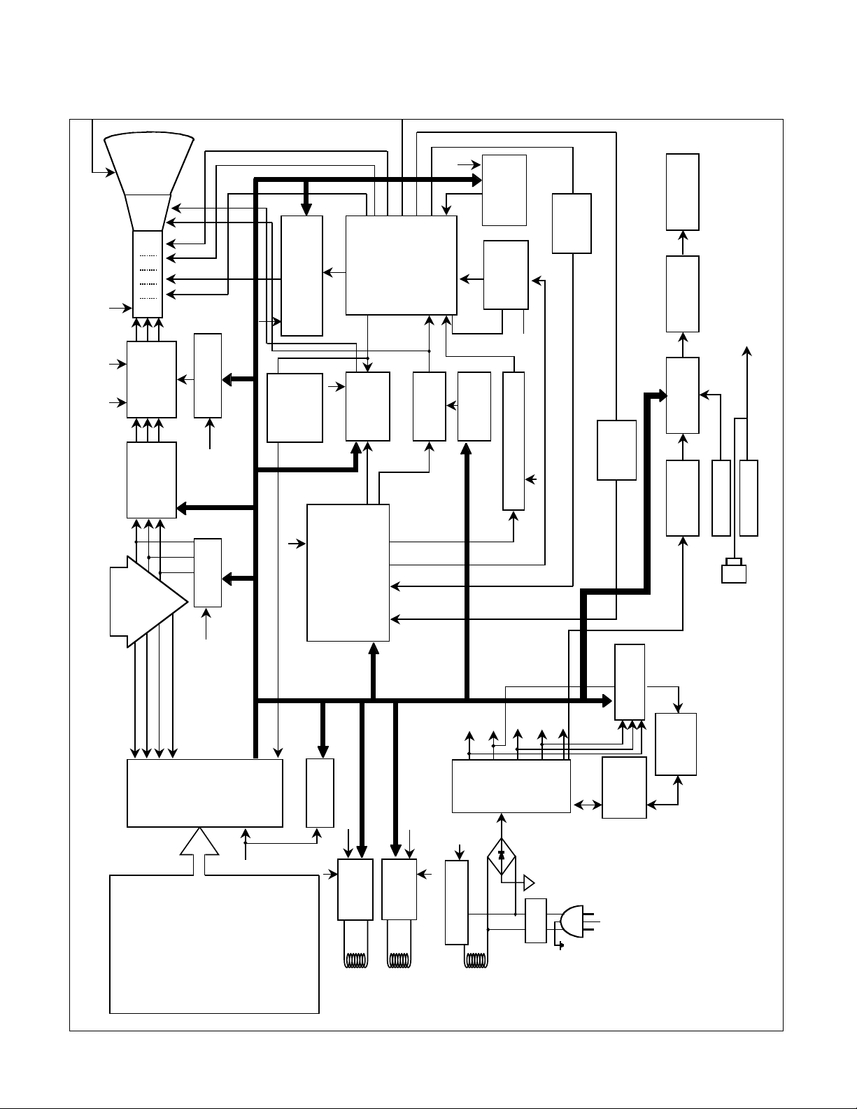
BLOCK DIAGRAM
- 12 -
Input Voltage
100~240VAC
(50/60Hz)
Line
Filter
Degaussing Cir.
[ OSD Con trol ]
Power
Control
IC
(IC901)
TILT
Control
Cir.
6.3V
15V
E
2
PROM
(IC402)
5V
OSD IC
(IC301)
H Sync. sig .
V Sync. Sig.
I
2
C DATA(SDA)
I
2
C CLOCK(SCL)
VIDEO
Pre Amp.
(IC302)
Input
Signal
RGB
VIDEO
Main Amp.
(IC303)
CUT OFF Circuit
(IC304)
80V
5V
Vertical Output
( IC601)
TDA4866J
H Defleciton
( Q706)
H-Linearity
Circuit.
Dynamic
Focus Cir.
- 120V
40V
15V
12V
MICOM
(IC401)
SCL / SDA
H/V Sync S ignal
PWM Control Signal
15V
15V
50V
DY CDT
Heater ( 6.3V )
I
2
C
I
2
C
I
2
C
H/V Sync
Signal
Screen
H.V
R/G/B
Bias
R/G/B
Contrast
H Drive
B-Drive
B+
15V
I
2
C
BRIGHTNESS/CONTRAST
COLOR CURVE
H / V POSITION
H / V SIZE
SPCC
TRAPEZOID
PIN BALANCE
PARALLELOGRAM
TILT
TOP CORNER
BOTTOM CORNER
RECALL
DEGAUSSING
MOIRE
LANGUAGE
Audio Control
-Volume
-Treble
-Bass
-Balance
-Microphone
Audio Mute
850V
15V
6.3V
12V 80V
PURITY
Control
Cir.
15V
6.3V
Degaussing Coil
Dynomic Focus
Static Focus
TILT
Coil
PURITY
Coil
50V
80V
5V
G2
G1
Auto Beam
Limit Circuit
DC/DC Converter
FBT
( T701 )
Regulation
Circuit
15V
SMPS
(T901)
Vertical Blanking,
Brightness Contorl
Circuit
X-RAY
Protection
Circuit
H/V Sync. Processor
( IC701 )
TDA4841
D/D
Feed Back
Energy Savi
Sound (15V)
ng
Control Cir
Voltage
Feedback
REGULATOR
(Q1)
AUDIO IN
TO PC
l C
2
9V
MIC
MIC OUT
AUDIO PRE-AMP
(IC1)
.
AUDIO MAIN-AMP
(IC2)
SPEAKER

DESCRIPTION OF BLOCK DIAGRAM
- 13 -
1. SMPS(Switching Mode Power Supply)
When you turn on the power switch, the operating
procedure is as follows:
1) The AC line voltage is rectified by the bridge diodes
D900 and C908
2) The control IC(IC901) starts switching and generates
switching pulses in the primary turns of the SMPS
transformer (T901)
3) The switching pulses of the primary turns induce the
secondary pulse of the transformer by the turn ratio.
These pulses are rectified by each diode
(D971,D961,D962,D951,D942, D941 and D901)
4) Each rectified DC voltage (80V, 50V, 15V, 6.3V, 5V and
Audio(15V)) is supplied to the main circuit.
2. Over Voltage Protection Circuit
When the input voltage of IC901 Vin(pin 7) is more than
Spec Voltage , all the secondary voltages of the SMPS
transformer (T901) down to low value.
3. Display Power Management Circuit
1) Stand-by and Suspend mode.
When no input of horizontal or vertical sync, Q972&
Q952 are turned off.. then input power consumption is
below 15 watts
2) OFF mode
When no input of horizontal and vertical sync, Q942 is
turned off and all the secondary voltages of the SMPS
transformer (T901) down to low value. Then input power
consumption is below 3 watts
4. X-ray Protection Circuit
If the high voltage of the FBT reaches up to 29KV IN an
abnormal case, Q807 operates and IC401 pin 19 came to
low level, then IC401 control IC701 to stop Horizontal
drive pulse and stop Horizontal deflection.
5. Microprocessor Control Circuit.
1) Horizontal and Vertical sync signals are supplied to the
microprocessor (IC401).
2) Microprocessor(IC401) discriminates the operating
mode from the sync. polarity and resolution..
3) After microprocessor reads these adjusted mode data
stored at EEPROM, it controls operating mode data
through IIC.
4) Users can control screen condition by the OSD, SET,
UP, DOWN, RIGHT and LEFT buttons.
6. D/D (DC to DC) Convert Circuit.
To obtain constant high voltage, this circuit supplies
controlled DC voltage for FBT and Horizontal deflection
circuit according to the horizontal sync frequency.
7. Horizontal and Vertical Sync Processor Circuit.
The horizontal and vertical sync processor IC (IC701) has
a sync detector, a saw-tooth generator, and drive
function. So output horizontal and vertical drive signal
control screen distortions.
8. Horizontal linearity Circuit.
This circuit corrects the horizontal linearity for each
horizontal sync frequency.
9. Horizontal drive and Output Circuit.
This circuit is a horizontal deflection amplifier for raster
scan.
10. ABL Circuit.
This circuit limits the beam-current for the reliability of the
CDT.
11. Vertical Output Circuit.
This circuit takes the vertical ramp wave from the
TDA4841(IC701) and performs the vertical deflection by
supplying the saw-tooth wave current to the vertical
deflection yoke.
12. Blanking and Brightness Control Circuit.
Blanking circuit eliminates the retrace line by supplying a
negative pulse wave to the G1 of the CDT. Brightness
control circuit is used for control of the screen brightness
by changing the DC level of the G1.
13. Video Processor Circuit.
Video processor circuit consists of the video drive output
block. The video drive IC(IC302) receives the video
signal from PC. The gain of each channel is controlled by
the voltage of contrast pin. The cut-off circuit compensate
different voltage of each channel between thecathode
and the G1 of the CDT.
14. OSD (On-Screen-Display) Circuit.
This circuit displays on the screen information of the
monitor's status.
15, Dynamic Focus Output Circuit.
This circuit takes the horizontal and the vertical parabola
waves from the TDA4866(IC701) and amplifies it to
maintain constant focus on center and corners in the
screen.
16. Image Rotation (Tilt) Circuit.
This circuit corrects the tilt of the screen by supplying the
image rotation signal to the tilt coil which is attached near
the deflection yoke of the CRT
17. Earth Magnetic Correction(Purity) Circuit
This circuit corrects the convergence of screen by
supplying the convergence signal to the Coil which is
attached to the CRT near the deflection
18. Audio circuit
The sound circuit get to the audio gain with the preamp(IC1) and the main amp(IC2).
The speaker maximum output is 3W.
If adjust to volume in OSD menu, the MICOM control to
IC1.
 Loading...