

Page 1

- 2 -
CONTENTS
MICRO COMPONENT SYSTEM
1. SERVICING PRECAUTIONS 3
2. ESD PRECAUTIONS 5
3. SPECIFICATIONS 6
4. ADJUSTMENTS 8
5. MAJOR WAVEFORM 11
6. TROUBLESHOOTING GUIDE 14
7. BLOCK DIAGRAM 19
8. SCHEMATIC DIAGRAM 20~23
• FRONT & KEY CIRCUIT 20
• AMP & DECK CIRCUIT 21
• TUNER CIRCUIT 22
• CDP CIRCUIT 23
9. WIRING DIAGRAM 24
10. PCB LAYOUTS 25~26
• MAIN P.C.BOARD 25
• CDP P.C. BOARD 26
11. INTERNAL BLOCK DIAGRAM OF ICs 27
12. EXPLODED VIEW/PARTS LIST 38~40
• CABINET 38
• TAPE DECK MECHANISM: AUTO STOP DECK 39
13. REPLACEMENT PARTS LIST 41~52
SPEAKER SYSTEM
1. SPECIFICATION 53
2. SCHEMATIC DIAGRAM 53
3. EXPLODED VIEW/PARTS LIST 54
Page 2
- 3 -
SERVICING PRECAUTIONS
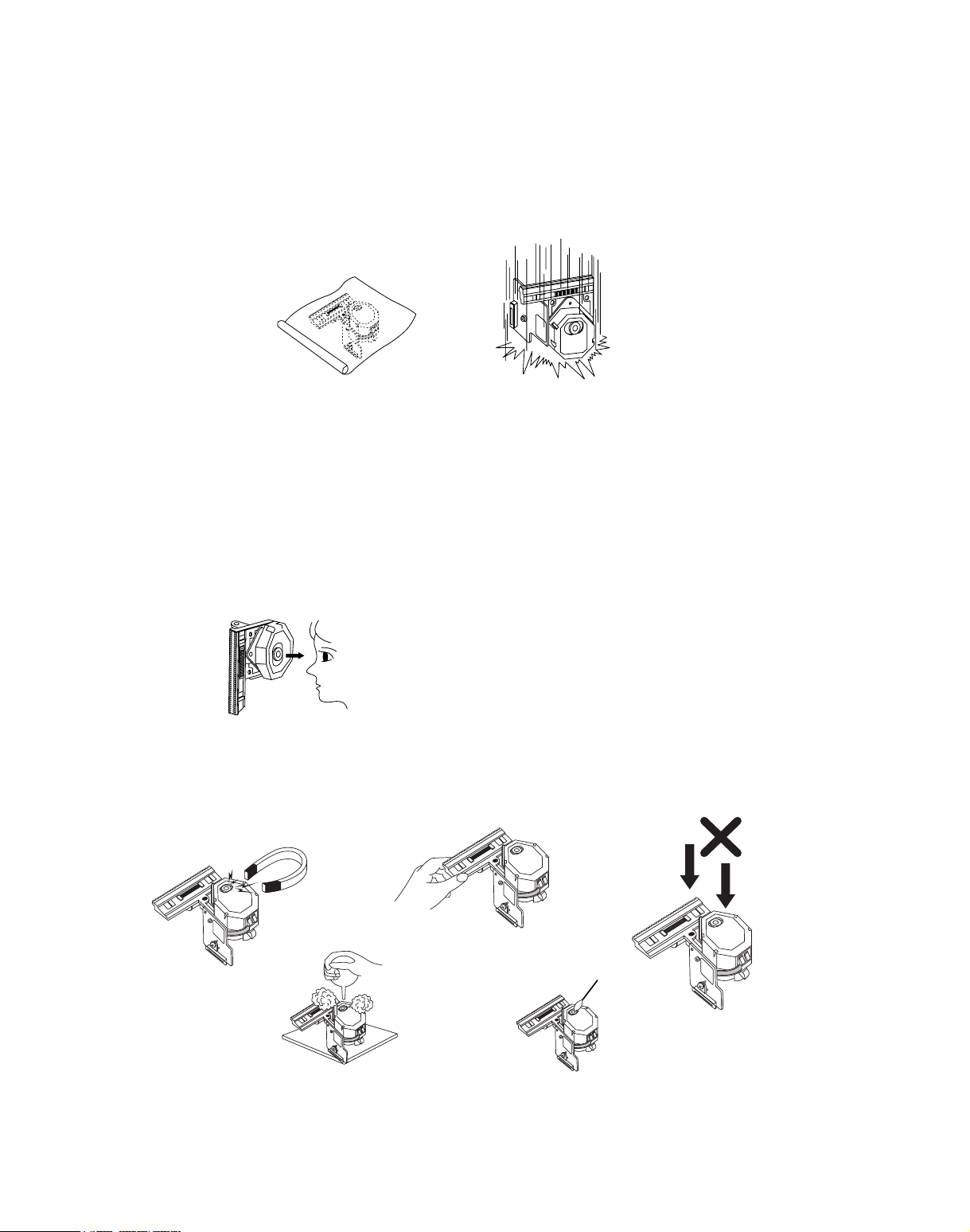
NOTES REGARDING HANDLING OF THE PICK-UP
1. Notes for transport and storage
1) The pick-up should always be left in its conductive bag until immediately prior to use.
2) The pick-up should never be subjected to external pressure or impact.
2. Repair notes
1) The pick-up incorporates a strong magnet, and so should never be brought close to magnetic materials.
2) The pick-up should always be handled correctly and carefully, taking care to avoid external pressure and
impact. If it is subjected to strong pressure or impact, the result may be an operational malfunction and/or
damage to the printed-circuit board.
3) Each and every pick-up is already individually adjusted to a high degree of precision, and for that reason
the adjustment point and installation screws should absolutely never be touched.
4) Laser beams may damage the eyes!
Absolutely never permit laser beams to enter the eyes!
Also NEVER switch ON the power to the laser output part (lens, etc.) of the pick-up if it is damaged.
5) Cleaning the lens surface
If there is dust on the lens surface, the dust should be cleaned away by using an air bush (such as used
for camera lens). The lens is held by a delicate spring. When cleaning the lens surface, therefore, a
cotton swab should be used, taking care not to distort this.
6) Never attempt to disassemble the pick-up.
Spring by excess pressure. If the lens is extremely dirty, apply isopropyl alcohol to the cotton swab. (Do
not use any other liquid cleaners, because they will damage the lens.) Take care not to use too much of
this alcohol on the swab, and do not allow the alcohol to get inside the pick-up.
Storage in conductive bag
Drop impact
NEVER look directly at the laser beam, and don’t let
contact fingers or other exposed skin.
Magnet
How to hold the pick-up
Pressure
Pressure
Cotton swab
Conductive Sheet
Page 3
- 4 -
NOTES REGARDING COMPACT DISC PLAYER REPAIRS
1. Preparations
1) Compact disc players incorporate a great many ICs as well as the pick-up (laser diode). These
components are sensitive to, and easily affected by, static electricity. If such static electricity is high
voltage, components can be damaged, and for that reason components should be handled with care.
2) The pick-up is composed of many optical components and other high-precision components. Care must
be taken, therefore, to avoid repair or storage where the temperature of humidity is high, where strong
magnetism is present, or where there is excessive dust.
2. Notes for repair
1) Before replacing a component part, first disconnect the power supply lead wire from the unit
2) All equipment, measuring instruments and tools must be grounded.
3) The workbench should be covered with a conductive sheet and grounded.
When removing the laser pick-up from its conductive bag, do not place the pick-up on the bag. (This is
because there is the possibility of damage by static electricity.)
4) To prevent AC leakage, the metal part of the soldering iron should be grounded.
5) Workers should be grounded by an armband (1MΩ)
6) Care should be taken not to permit the laser pick-up to come in contact with clothing, in order to prevent
static electricity changes in the clothing to escape from the armband.
7) The laser beam from the pick-up should NEVER be directly facing the eyes or bare skin.
Armband
Conductive
Sheet
Resistor
(1 Mohm)
Resistor
(1 Mohm)
Page 4
- 5 -
ESD PRECAUTIONS
Electrostatically Sensitive Devices (ESD)
Some semiconductor (solid state) devices can be damaged easily by static electricity. Such components
commonly are called Electrostatically Sensitive Devices (ESD). Examples of typical ESD devices are integrated
circuits and some field-effect transistors and semiconductor chip components. The following techniques should
be used to help reduce the incidence of component damage caused by static electricity.
1. Immediately before handling any semiconductor component or semiconductor-equipped assembly, drain off
any electrostatic charge on your body by touching a known earth ground. Alternatively, obtain and wear a
commercially available discharging wrist strap device, which should be removed for potential shock reasons
prior to applying power to the unit under test.
2. After removing an electrical assembly equipped with ESD devices, place the assembly on a conductive
surface such as aluminum foil, to prevent electrostatic charge buildup or exposure of the assembly.
3. Use only a grounded-tip soldering iron to solder or unsolder ESD devices.
4. Use only an anti-static solder removal device. Some solder removal devices not classified as "anti-static" can
generate electrical charges sufficient to damage ESD devices.
5. Do not use freon-propelled chemicals. These can generate electrical charges sufficient to damage ESD
devices.
6. Do not remove a replacement ESD device from its protective package until immediately before you are
ready to install it. (Most replacement ESD devices are packaged with leads electrically shorted together by
conductive foam, aluminum foil or comparable conductive materials).
7. Immediately before removing the protective material from the leads of a replacement ESD device, touch the
protective material to the chassis or circuit assembly into which the device will by installed.
CAUTION : BE SURE NO POWER IS APPLIED TO THE CHASSIS OR CIRCUIT, AND OBSERVE ALL OTHER
SAFETY PRECAUTIONS.
8. Minimize bodily motions when handing unpackaged replacement ESD devices. (Otherwise harmless motion
such as the brushing together of your clothes fabric or the lifting of your foot from a carpeted floor can
generate static electricity sufficient to damage an ESD device).
[CAUTION. GRAPHIC SYMBOLS]
THE LIGHTNING FLASH WITH APROWHEAD SYMBOL. WITHIN AN EQUILATERAL
TRIANGLE, IS INTENDED TO ALERT THE SERVICE PERSONNEL TO THE PRESENCE
OF UNINSULATED “DANGEROUS VOLTAGE” THAT MAY BE OF SUFFICIENT
MAGNITUDE TO CONSTITUTE A RISK OF ELECTRIC SHOCK.
THE EXCLAMATION POINT WITHIN AN EQUILATERAL TRIANGLE IS INTENDED TO
ALERT THE SERVICE PERSONNEL TO THE PRESENCE OF IMPORTANT SAFETY
INFORMATION IN SERVICE LITERATURE.
Page 5
- 8 -
ADJUSTMENTS
This set has been aligned at the factory and normally will not require further adjustment. As a result, it is not
recommended that any attempt is made to modificate any circuit. If any parts are replaced or if anyone tampers
with the adjustment, realignment may be necessary.
ADJUSTMENT & TEST POINT
Figure 1. Main P.C. Board
L140
(RECORD BIAS
ADJUSTMENT)
L21
(FM IF
ADJUSTMENT)
Page 6
- 9 -
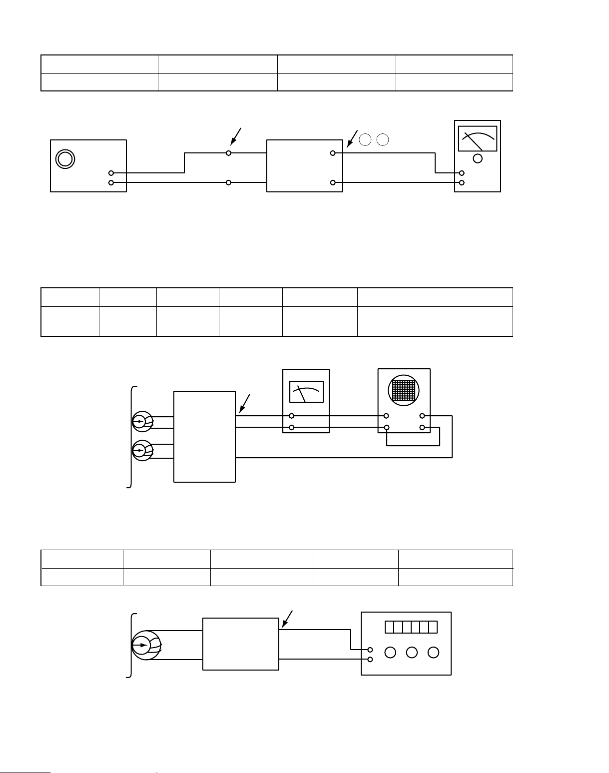
TAPE DECK ADJUSTMENT
1. AZIMUTH ADJUSTMENT
Figure 3. Azimuth Adjustment Connection Diagram
2. RECORD BIAS ADJUSTMENT
Figure 4. Record Bias Adjustment Connection Diagram
TUNER ADJUSTMENT
Figure 2. Tuner(S curve) Adjustment Connection Diagram
CH1 CH2
Speaker
Terminal
Playback Mode
Head
Test Tape
MTT-114
L ch
R ch
GND
Dual-trace
synchroscope
Electronic
Voltmeter
L out
R out
Unit
Unit
26
,
28 PIN
Signal Generator
GND
Electronic
OSCILLOSCOPE
FM Antenna
Terminal
Deck Mode Test Tape Test Point Adjustment Adjust for Remark
Playback MTT-114
Speaker
Head Screw R/L Maximum
Forward:Righthand Side Screw
Terminal Reverse:Lefthand Side Screw
Item Test Point Adjustment Adjust for
DC Voltage IC10 26, 28 pin L21 0V
±50mV
Deck Mode Test Tape Test Point Adjustment Adjust for
Rec/Pause MTT-5511 Erase Head Wire L140 83kHz±5kHz
Head
Test Tape
MTT-5511
Record/Playback
Head
Record/Playback
and Pause Mode
Unit
Erase Head Wire
GND
Frequency Counter
Page 7
- 10 -
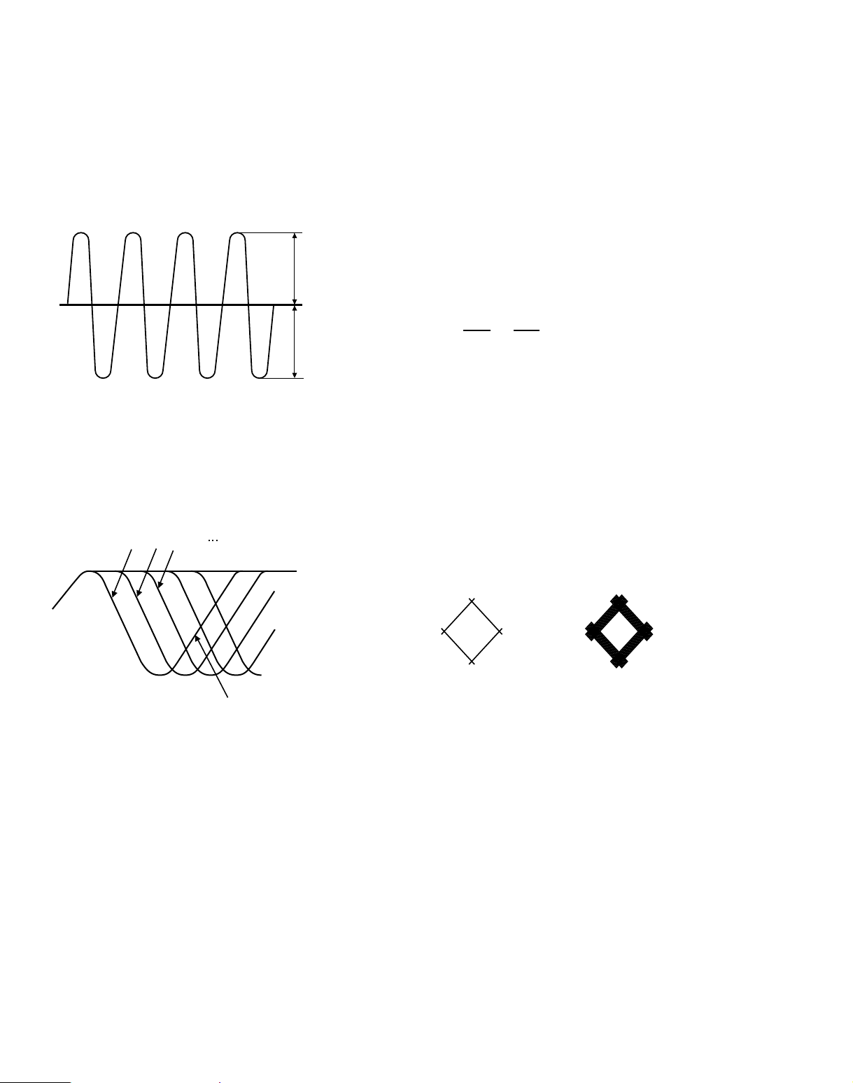
CDP ADJUSTMENTS
• When change the pick-up must be confirm as follow
1. TRACKING BALANCE CONFIRMATION
1) Connect the oscilloscope to TEO and REF.(IC501 pin 54 and 71)
2) Access from 1st selection to last section of test disc (YEDS-18)
3) Confirm the normal state of tracking error signal (T.B deviation : less than ±3%)
2. RF WAVEFORM CONFIRMATION
1) Connect the oscilloscope to RF and REF.(IC501 pin 74 and 71)
2) Put a test disc (SONY YEDS-18) into unit and playback the 18th selection of the test disc.
3) Confirm the normal state of RF waveform.
4) Confirm the less than 30nS of Jitter Meter reading.
OV(DC Mode) T.B deviation(%)
= X %
A
B
A=B
A+B
A-B
2
100
3T, 4T 5T,6T 11T
EYE-PATTERN EYE-PATTERN
OK NG
Page 8
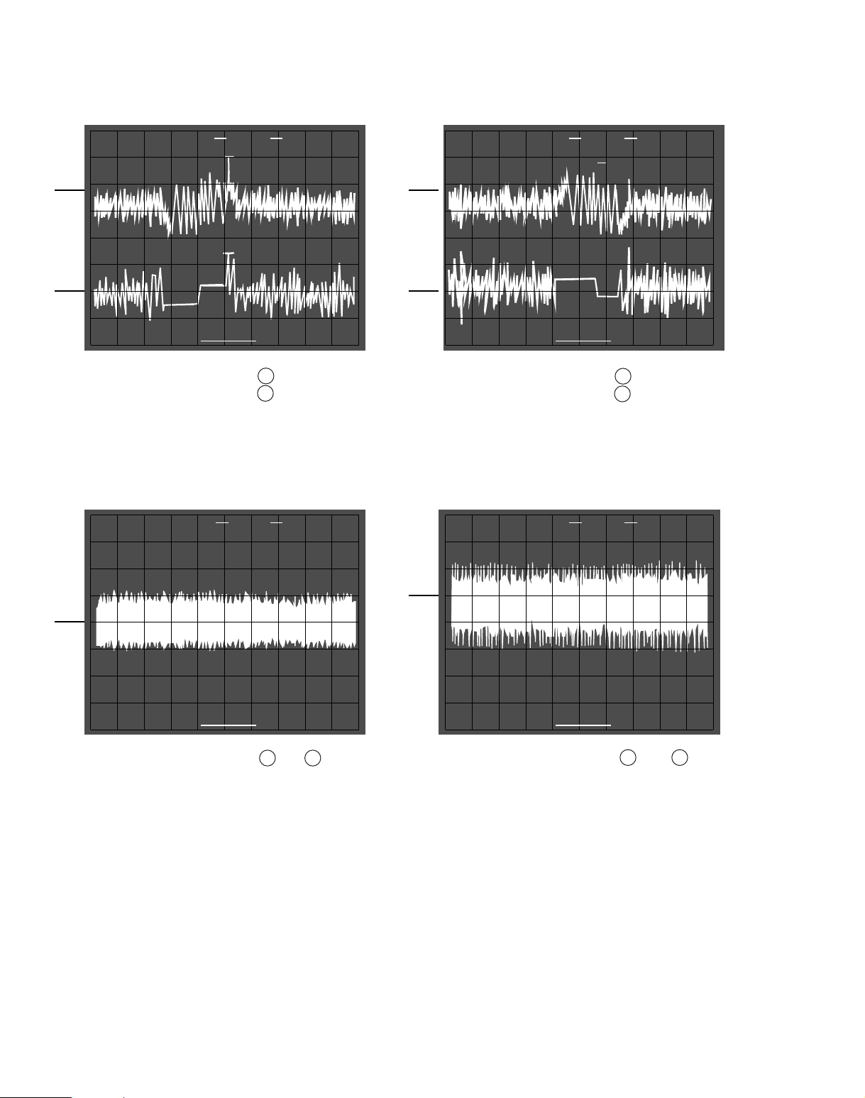
- 11 -
• Connection : 1. IC501 pin 54.(TEO)
2. IC501 pin 50
• Inspection : Check tracking servo
circuit.(RWD)
• Connection : 1. IC501 pin 54 .(TEO)
2. IC501 pin 50
• Inspection : Check tracking servo
circuit.(RWD)
FOCUS GAIN TRACKING GAIN
• Connection : 3. IC502 pin 1 and 2 .
• Test disc : YEDS-43
• Inspection : Confirm focus servo circuit.
• Connection : 3. IC502 pin 26 and 27 .
• Test disc: YEDS-43
• Inspection : Confirm TRACK servo circuit.
TRACKING ERROR(REW) TRACKING ERROR(FWD)
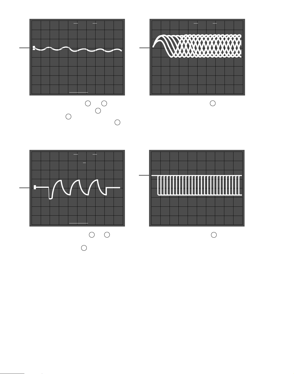
MAJOR WAVEFORM
∆V1=0.00V TRIG 1=1.0V
∆V2=0.00V
DLY>=0.85ms
1V 1V PEAKDET 1ms 1ms
SAVE
∆T=0.00ms
∆V1=0.00V TRIG 2=1.0V
∆V2=0.00V SREF 2 A
DLY>=0.85ms
1V 1V PEAKDET 1ms 1ms
∆T=0.00ms
∆V1=0.000V TRIG 1=0.09V
DLY>=4.25ms
0.5V PEAKDET 5ms 5ms
SAVE
∆T=0.00ms
∆V1=0.0% TRIG 1=-82%
DLY>=0.170s
>1V PEAKDET 0.2s 50ms
SAVE
∆T=0.000s
1
2
3
4
1
2
Page 9
- 12 -
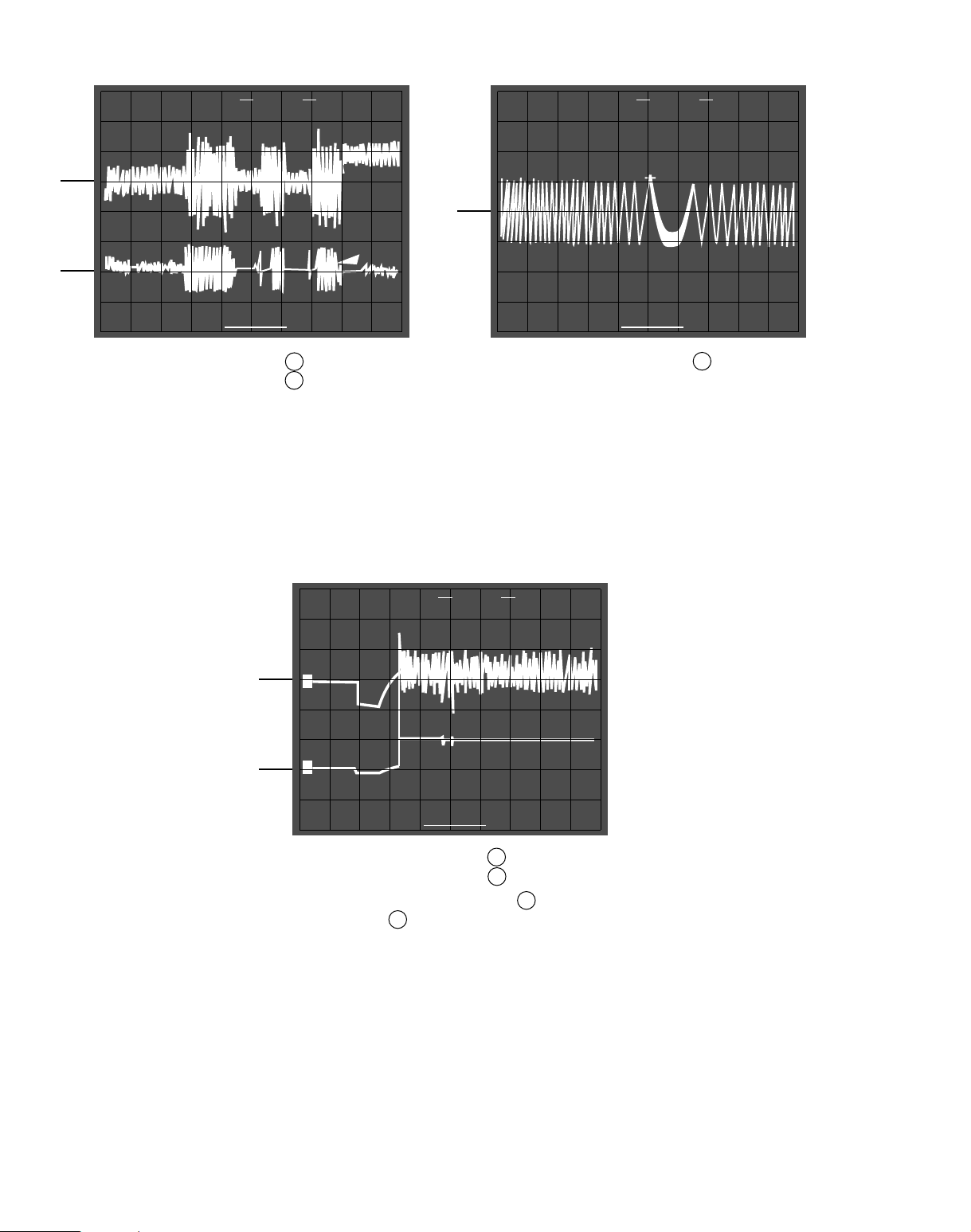
TRACKING COIL DRIVE E.F. BALANCE
• Connection : 1. IC501 pin 54 . (TEO)
2. IC501 pin 50
• Inspection : - Confirm tracking servo circuit.
- Check IC501 (Cold solder joint
or short circuit)
• Connection : 1. IC501 pin 54 .
• Inspection : Confirm tacking servo balance
deviation rate
READING
• Connection : 7. IC501 pin
48 .
8. IC501 pin
40 (FOK)
• Inspection : Check IC502 pin 4 to IC501 PIN
48 (Pattern defective)
∆V1=0.00V TRIG 1=-0.1V
∆V2=0.00V
DLY>=0.425s
1V 2V PEAKDET 0.5s 50ms
SAVE
∆T=0.000s
∆V1=3.96V TRIG 1=1.1V
DLY>=1.70ms
1V PEAKDET 2ms 2ms
SAVE
∆T=0.00ms
∆V1=0.00V TRIG 1=0.2V
∆V2=0.00V
DLY>=0.425s
2V 5V PEAKDET 0.5s 50ms
SAVE
∆T=0.000s
1
1
2
7
8
Page 10
- 13 -
• Connection : 9. IC502 pin 17 and 18
• Inspection : - Check IC501 pin 43 to IC502
pin 20 (Pattern defective)
- Check voltage. (IC502 pin 20 )
• Connection : 10. IC501 pin 74 .
• Inspection : Check objective Lens of Pickup
clear or not
• Connection : 11. IC502 pin 1 and 2 .
• Inspection : - Is focus search signal output to
IC501 pin 48 ?
• Connection : 12. IC501 pin 33 .
• Inspection : Check IC503 and surrounding
circuit (Cold solder joint or short
circuit)
TRIG 1=1.1V
∆V2=0.000V
DLY>=0.085s
0.5V PEAKDET 0.1s 50ms
SAVE
∆T=0.000s
TRIG 1=24%
DLY>=0.670ms
50mV 0.5ms 0.5ms
∆V1=0.00V TRIG 1=0.3V
DLY>=0.085s
2V PEAKDET 1s 50ms
SAVESREF 3 A
∆T=0.00s
>2V
9
11
12
10
Page 11
- 14 -
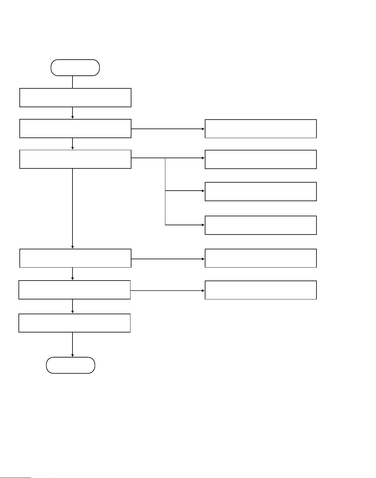
TROUBLESHOOTING GUIDE
CD PART
Is the function selector in the CD position?
Is power turned ON?
Does initial reading occur?
Can disc be played?
Is audio output supplied?
OK
END
• Check power supply circuitry.
• Check laser circuitry.
• Check focusing circuitry.
• Check disc.
• Check tracking servo circuitry.
• Check Audio circuitry.
YES
YES
YES
YES
YES
NO
NO
NO
NO
Page 12
- 15 -
1-1.8V
2.5V
1. If initial reading is not carried out (with disc)
YES
YES
YES
YES
YES
YES
YES
YES
YES
NO
NO NO
NO NO
NO
NO
NO
NO
NO
NO
Is IC601 pin 22 output
waveform normal?
Door open
(3.2V~5V)
Door close(1.9V~2.5V)
Does laser light?
• Leaf SW contact defective.
• Connector defective.
• Pattern short.
Does disc motor rotate?
Is HF
waveform
output?
IC501 pin 74
Is tracking servo
operating?
Is the lower
envelope of HF
(RF) waveform
flat?
Is signal output
at IC501 pin
50?
Is signal output at tracking
output IC502 pin 26, 27?
Does IC503 pin 25 (LKFS) as
figure?
Is retation normal?
Is there any irregularity in
frequency?
Is HF signal normal without
dropout?
Is TER signal
output, at
IC501 pin
54?
• IC501
defective.
• Connector
defective.
• Pick up
defective.
• Pattern
defective.
• IC502 or pattern
defective.
• Pick up
defective.
• Connector
defective.
• IC501 or IC503
defective.
• PLL CIRCUIT
defective.
• Disc initial reading
damaged or
defective.
• CLV
SERVO(R530,
C535, C536, R531)
circuit defective.
Page 13

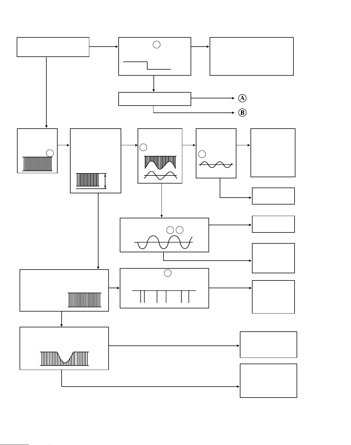
- 16 -
A
NO
NO
NO
NO
NO
NO
NO
NO
NO
When laser does not light
Is below signal “H” at IC501 pin
38 (RESET)?
Has Laser Power source returned to
the Q501?
(Q501 Collector Voltage about 1.8V)
Does generate about 3.3V at IC501
pin 70 (LD)?
Flow Laser Current?
Both voltage of 507 is about 1.0V?
Are data transferred from
IC601?
IC601 pin 95 : XLT
pin 94 : XRST
pin 98
: DATA
pin 97: CLK
Is below signal output at
IC502 pin 17, 18?
• IC601 defective.
• IC501 defective.
•
Surrounding Circuitry defective.
• Connector defective.
• Pick-up defective.
• IC501, 502 defective.
• Slide motor defective.
• Connector defective.
• IC505 defective.
• LMT SW defective.
• Connector defective.
• IC502 defective.
•
Q501 defective, connector defective.
• Laser defective.
• Laser defective.
•
Connector defective. short etc.
Has Pick-up returned to the
innermost position?
Does pick-up stop after
having moved to the
innermost position?
Are detect output input at
IC601 pin 22?
R507»1.0V
R507«1.0V
YES
YES
YES
YES
(2.5V)
OPEN
CLOSE
(1.95V)
YES
YES
YES
YES
YES
YES
[
Page 14

- 17 -
B
C
Amplitude 0.5~1.5v
IC501 Pin
74
HF
FOK
IC501 Pin
40
Do lenses move up and down?
Is signal output at focus
search terminal?
IC 501 pin 48 (FEO)
Is signal output at IC502
pin 1 , 2 ?
When laser light
• IC501 defective.
• C527 defective.
• IC 502 defective.
• IC501 defective.
• Pattern defective.
• Actuator short.
• Connector short.
• Connector short.
• IC501 defective.
• Pick-up defective.
• Turntable height error
• Laser diode degraded.
Is IC501 pin 74 (HF) signal waveform
output?
The waveform of IC501 pin 74 (HF) is
below figure?
Is Fok signal intput to IC601 pin 99 ?
Is Fok signal output?
(HF and REF) 0.4 over OK.
YES
YES
YES
YES
YES
YES
YES
NO
NO
NO
NO
NO
NO
NO
Page 15

- 18 -
FER
SENSE
(ISTAT)
C
at Start
Is FER signal output? IC501 Pin 59?
Is FZC signal output at IC501 Pin 31
(SENS)?
Is Mon signal output by
IC503 Pin 73?
Is MDP signal output by
IC503 Pin 75?
Has voltage at disc motor?
(IC502 pin 11, 12 )
• IC501 defective.
• Pick up defective.
• Connector defective.
• IC501 defective.
• Pattern defective between.
• IC503 Pin 27,36,37,38 and IC601.
• IC501, 502 defective.
• Surrounding circuity defective.
• Disc Motor defective.
• Connector defective.
When Fok focus
Servo Conform by
FZC signal
NO
NO
NO
NO
YES
YES
YES
YES
YES
Page 16

- 28 -
■ LC72131, 72131M
B01 B02 B03 B04 I01 I02
XIN
PD
AIN
AOUT
IFIN
XOUT
FMIN
AMIN
CE
DI
CL
D0
VDD
VSS
REFERENCE
DIVIDER
PHASE DETECTOR
CHARGE PUMP
UNLOCK
DETECTOR
UNIVERSAL
COUNTER
DATA SHIFT REGISTER
LATCH
12bits PROGRAMMABLE
DIVIDER
SWALLOW COUNTER
1/16. 1/17 4bits
POWER
ON
RESET
C B
I/F
1
2
2
■ TDA7440D
L-IN1
100K
100K
100K
100K
100K
100K
100K
100K
48918
27
21
22
20
26
24
25
LOUT
SCL
SDA
DIG_GND
ROUT
V
S
AGND
R
B
R
B
14 15
10 11 19 12 13 23
5
G
G
6
7
3
2
INPUT MULTIPLEXER
+GAIN
MUXOUTR INR TREBLE(R) BIN(R) BOUT(R) CREF D98AU883
0/30dB
2dB STEP
MUXOUTL
VOLUME TREBLE
I CBUS DECODER + LATCHES
BASS
SPKR ATT
LEFT
VOLUME TREBLE BASS
SUPPLY
V
REF
SPKR ATT
RIGHT
INL TREBLE(L) BOUT(L)BIN(L)
1
28
L-IN2
L-IN3
L-IN4
R-IN1
R-IN2
R-IN3
R-IN4
2
Page 17

- 29 -
■ KB9223(IC501)
OVERVIEW
The KB9223 is a 1-chip BICMOS intergrated circuit to perform the
function of RF AMP and Servo signal processor for compact disc
player application. It consist of blocks for RF signal processing,
focus, tracking, sled and spindle servo. Also this IC has adjustment
free function and embeded opamp for audio post filter.
FEATURES
• RF amplifier & RF equalizer
• Focus error amplifier & servo control
• Tracking error amplifier & servo control
• Mirror & Defect detector circuit
• Focus OK detrector circuit
• APC(Auto Laser Power Control) circuit for constant laser power
• FE bias & focus servo offset adjustment free
• EF balance & tracking error gain adjustment free
• Embeded audio post filter
• The circuit for Interruption countermeasure
• Double speed play available
• Operating voitage range 3.4V~5.5V
PIN CONFIGURATION
#1
ORDERING INFORMATION
APPLICATIONS
• CD PLAYER
• Video-CD
RELATED PRODUCT
• KS9286 Data Processor
• KS9284 Data Processor
• KS9258D/KA9259D Motor Driver
Device Package Tempe. Range
KB9223 80-QFP-1420C -20~+70˚C
80-QFP-1420C
51
52
53
54
55
56
57
58
59
60
61
62
63
64
TE2
65
PD1
66
PD2
67
F
68
E
69
PD
70
LD
71
VR
72
AVCC
73
RF-
74
RFO
75
IRF
76
ARF
77
RF1
78
CAGC
79
EI
80
AVEE
1
DVEE
MCP
2
TG2
FEBIAS
FRSH
DCB
3
4
TGU
DCC2
5
FE1
FDFCT
FSET
DCC1
6
AVCC
7
TDFET
VCCP
8
9
FE2
TE1
LPFT
DVCC
KB9223
CH21
GC20
GC21
12
11
10
CH20
13
TZC
CH10
14
43
44
45
46
47
48
49
50
ATSC
CH1I
15
TEO
CH10
16
TE-
CH1I
17
FEO
RRC
18
FE-
VSSP
19
SPDL-
SPDLD
ISET
MUTEI
20
21
SL-
VREG
22
SLO
WDCH
42
SL+
SMDP
23
41
SSTOP
SMON
24
FOK
MIRROR
RESET
MLT
MDATA
MCK
AVEE
EFM
ASY
ISTAT
TRCNT
LOCK
FGD
FS3
FLB
SMEF
40
39
38
37
36
35
34
33
32
31
30
29
28
27
26
25
Page 18

- 30 -
Pin No.
Symbol Description
1 MCP Capacitor connection pin for mirror hold
2 DCB Capacitor connection pin for defect Bottom hold
3 FRSH Capacitor connection pin for time constant to generate focus search waveform
4 DCC2 The input pin through capacitor of defect bottom hold output
5 DCC1 The output pin of defect bottom hold
6 FSET The peak frequency setting pin for focus, tracking servo and cut off frequency of CLV LPF
7 VDDA Analog ACC for servo part
8 VCCP VCC for post filter
9 GC2I Amplifier negative input pin for gain and low pass filtering of DAC output CH2
10 GC2O Amplifier output pin for gain and low pass filtering of DAC output CH2
11 CH2I The input pin for post filter channel2
12 CH2O The output pin for post filter channel2
13 CH1O The output pin for post filter channel1
14 CH1I The input pin for post filter channel1
15 GC1O Amplifier output pin for gain and low pass filtering of DAC output CH1
16 GC1I Amplifier negative input pin for gain and low pass filtering of DAC output CH1
17 RRC The pin for noise reduction of post filter bias
18 VSSP VSS for post filter
19 MUTEI The input pin for post filter muting control
20 ISET The input pin for current setting of focus search, track jump and sled okick voltage
21 VREG The output pin of regulator
22 WDCK The clock input pin for auto sequence
23 SMDP The input pin of CLV control output pin SMDP of DSP
24 SMON The input pin for spindle servo ON through SMON of DSP
25 SMEF The input pin of provide for an external LPF time constant
26 FLB Capacitor connection pin to perform rising low bandwidth of focus loop
27 FS3 The pin for high freqency gain change of focus loop with internal FS3 switch
28 FGD Reducing high freqency gain with capacitor between FS3 pin
29 LOCK Sled runaway prevention pin
30 TRCNT Track count output pin
31 ISTAT Internal status output pin
32 ASY The input pin for asymmetry control
33 EFM EFM comparator output pin
34 VSSA Analog VSS for servo part
35 MCK Micom clock input pin
PIN DESCRIPTION
Page 19

- 31 -
Pin No.
Symbol Description
36 MDATA Micom data input pin
37 MLT Micom data latch input pin
38 RESET Reset input pin
39 MIRROR The mirror output for test
40 FOK The output pin of focus OK comparator
41 SSTOP The pin for detection whether pick_up position is innermost or ton
42 SL+ The noninverting input pin of sled servo amplifier
43 SLO The output pin of sled servo amplifier
44 SL- The inverting input pin of sled servo amplifier
45 SPDL- The noninverting input pin of spindle servo amplifier
46 SPDLO The output pin of spindle servo amplifier
47 FE- The inverting input pin of focus servo amplifier
48 FEO The output pin of focus servo amplifier
49 TE- The inverting input pin of tracking servo amplifier
50 TEO The output pin of tracking servo amplifier
51 ATSC The input pin for Anti-shock detection
52 TZC The comaparator input pin for tracking zero crossing detection
53 TE2 Tracking servo input pin
54 TE1 Tracking error amplifier output pin
55 LPFT The input pin of tracking error low pass filtering signal
56 DVDD The power supply pin for logic circuit
57 TDFCT The capacitor connection pin for tracking defect compensation
58 FE2 Focus servo input pin
59 FE1 Focus error amplifier output pin
60 FDFCT The capacitor connection pin for focus defect compensation
61 TGU The capacitor connection pin for high frequency tracking gain switch
62 TG2 The pin for high frequency gain change of tracking servo loop with internal TG2 switch
63 FEBIAS Focus error bias voltage control pin
64 DVEE The DVEE pin for logic circuit
65 PD1 The negative input pin of RF I/V amplifier1 (A+C signal)
66 PD2 The negative input pin of RF I/V amplifier2 (B+D signal)
67 F The negative input pin of F I/V amplifier1 (F signal
68 E The negative input pin of E I/V amplifier1 (E signal)
69 PD The input pin for APC
70 LD The output pin for APC
PIN DESCRIPTION (Continued)
Page 20

- 32 -
BLOCK DIAGRAM
MICOM TO SERVO CONTROL
AUTO SEQUENCER
FOK DETECTION
CIRCUIT
MIRROR DETECTION
CIRCUIT
Spindle Servo LPF
(Double Speed)
Sled Servo Amplifier
& Sled Kick GEN.
Tracking Phase
Compensation Block
& Jump Pulse GEN.
Focus Phase
Compensation
& Offset cancel circuit
Micom Data
Interface Logic
RF Amp
73
74
65
66
63
67
68
79
69
70
71
78
76
75
32
33
77
2
4
RF-
RFO
PD1
PD2
F
E
EI
PD
LD
VR
ARF
IRF
ASY
EFM
RFI
DCB
DCC1
GC1O
MLT
TZC
FE2
FLB
FGD
FS3
TE1
FE1
GC1I
CH1O
CH1I
MUTEI
RRC
CH2O
CH2I
GC2I
GC2O
5
15 16 13 14 19 17 12 11 9 10
40
1
39
6
25
24
23
45
46
42
44
43
61
62
55
53
50
49
57
48
47
60
FOK
MCP
MIRROR
FSET
SMEF
SMON
FS1 to
FS4
TM1 to
TM6
BAL1 to
BAL5
PS1 to
PS4
GA1 to
GA5
SMDP
SPDL-
SPDLO
SL+
SL-
SLO
TGU
TG2
LPFT
TE2
TEO
TE-
TDFCT
FEO
FE-
FDFCT
327282658525135363738312930225459
APC Amp
Center Voltage Amp.
Focus Error Amp
FE-BIAS Adjustment
Tracking Error Amp
E/F Balance & Gain
Control
RF Level AGC
&
Equalizer
EFM
Comparator
Defect Detection
CircuitT
ADJUSTMENT-FREE CONTROL
Built-in Post Filter Amp(L&R)
LDON
Pin No.
Symbol Description
71 VR The output pin of (AVEE+AVCC)/2 voltage
72 VCC VCC for RF part
73 RF- RF summing amplifier inverting input pin
74 RFO RF summing amplifier output pin
75 IRF The input pin for AGC
76 ARF The output pin for AGC
77 RFI The input pin for EFM comparating
78 CAGC The capacitor connection pin for AGC
79 EI Feedback input pin of E I/V amplifier for EF Balance control
80 GND GND for part
PIN DESCRIPTION (Continued)
Page 21

- 33 -
■ LA1837
Page 22

- 34 -
■ KB9286
DIGITAL SIGNAL PROCESSOR
The KS9286 is a CMOS integrated circuit designed for the Digital
Audio Signal Processor for Compact Disc Player. It is a monolithic
IC that builts-in 16 bit Digital Analog Convertor, ESP interface and
Digital De-emphasis additional conventional DSP function.
FEATURES
• EFM data demodulation
• Frame sync datection/protection/insertion
• Powerful error correction (C1 : 2error, C2 : 4erasure)
• Interpolation
• 8fs digital filter (51th+13th+9th)
• Subcode data serial output
• CLV servo controller
• Micom interface
• Digital audio output
• Digital de-emphasis
• ESP interface
• Built-in 16K SRAM
• Built-in Digital PLL
• Double speed play available
• Built-in 16 bit D/A converter
• VDD = 3.4 ~ 5.5V
PIN CONFIGURATION
DB6
40
DB7
39
DB8
38
MCK
37
MDAT
36
MLT
35
MUTE
34
DVDD1
33
SDAT
32
SBCK
31
SQOK
30
SQDT
29
SQCK
28
/ESP
27
S0S1
26
LKFS
25
SMEF
65
TEST1
66
EFMI
67
ADATAI
68
/ISTAT
69
TRCNT
70
LOCK
71
PBFR
72
SMEF
73
SMON
74
DVDD2
75
SMDP
76
SMSD
77
BCKI
78
TESTV
79
DSPEED
80
LRCHI
41
DB5
42
DB4
43
DB3
44
DB2
45
DB1
46
C1F1
47
C1F2
48
C2F1
49
C2F2
50
C2FL
51
/PBCK
52
DVSS2
53
FSDW
54
ULKFS
55
/JIT
56
C4M
57
C16M
58
/WE
59
/CS
60
XTALSEL
61
TEST0
62
CDROM
63
SRAM
64
EMPH
24
VREFH2
23
VREFH1
22
AVSS2
21
LCHOUT
20
RCHOUT.
19
AVDD2
18
VREFL2
17
VREFL2
16
C2PO
15
BCKO
14
DVSS1
13
ADATAO
12
LRCHO
11
WDCHO
10
XOUT
9
XIN
8
DATX
7
AVSS1
6
CNTVOL
5
DPFOUT
4
DPFIN
3
DPDO
2
AVDD1
1
KS9286
ORDERING INFORMATION
#1
Device Package Tempe. Range
KB9286 80-QFP-1420C -20~+75˚C
80-QFP-1420C
Page 23

- 35 -
PIN NO
SYMBOL IO DESCRIPTION
1 AVDD1 - Analog VCC1
2 DPDO O Charge pump output for Digital PLL
3 DPFIN I Filter input for Digital PLL
4 DPFOUT O Filter output for Digital PLL
5 CNTVOL I VCO control voltage for Digital PLL
6 AVSS1 - Analog Ground1
7 DATX O Digital Audio output data
8 XIN I X’tal oscillator input
9 XOUT O X’tal oscillator output
10 WDCHO O Word clock output of 48 bit/Slot (88.2KHz)
11 LRCHO O Channel clock output of 48 bit/Slot (44.1KHz), 88.2KHz when ESP ON
12 ADATAO O Serial audio data output of 48 bit/Slot(MSB first), double speed output when ESP ON
13 DVSS1 - Digital Ground1
14 BCKO O Audio data bit clock output of 48 bit/Slot (2.1168MHz), 4.2336MHz when ESP ON
15 C2PO O C2 Pointer for output audio data
16 VREFL2 I Input terminal2 of reference voltage “L” (Floating)
17 VREFL1 I Input terminal1 of reference voltage “L” (GND connection)
18 AVDD2 - Analog VCC2
19 RCHOUT O Right-Channel audio output through D/A converter
20 LCHOUT O Left-Channel audio output through D/A converter
21 AVSS2 - Analog ground2
22 VREFH1 I Input terminal1 of reference voltage “H” (VDD connection)
23 VREFH2 I Input terminal2 of reference voltage “H” (Floating)
24 EMPH O Emphasis/Non-Emphasis output, H:Emphasis ON, L:Emphasis OFF
25 LKFS O The Lock Status output of frame sync
26 S0S1 O Output of subcode sync signal (S0+S1)
27 RESET I System reset at “L”
28 /ESP I ESP function ON/OFF control (“L”:ESP function ON, “H”:ESP function OFF)
29 SQCK I Clock for output Subcode-Q data
30 SQDT O Serial output of Subcode-Q data
31 SQOK O The CRC (Cycle Redundancy Check) check result signal output of Subcode-Q
32 SBCK I Clock for output subcode data
33 SDAT O Subcode serial data output
34 DVDD1 - Digital VDD1
35 MUTE I Mute control input (“H”: Mute ON)
PIN DESCRIPTION
Page 24

- 36 -
PIN NO
SYMBOL IO DESCRIPTION
36 MLT I Latch Signal Input from Micom (Schmit Trigger)
37 MDAT I Serial data input from Micom (Schmit Trigger)
38 MCK I Serial clock input from Micom (Schmit Trigger)
39 DB8 I/O SRAM data I/O port 8 (MSB)
40 DB7 I/O SRAM data I/O port 7
41 DB6 I/O SRAM data I/O port 6
42 DB5 I/O SRAM data I/O port 5
43 DB4 I/O SRAM data I/O port 4
44 DB3 I/O SRAM data I/O port 3
45 DB2 I/O SRAM data I/O port 2
46 DB1 I/O SRAM data I/O port 1 (LSB)
47 C1F1 I/O Monitoring output for C1 error correction (RA1)
48 C1F2 I/O Monitoring output for C1 error correction (RA2)
49 C2F1 I/O Monitoring output for C2 error correction (RA3)
50 C2F2 I/O Monitoring output for C2 error correction (RA4)
51 C2FL1 I/O C2 decoder flag (RA5, “H”:When the processing C2 code is impossible correction
status.)
52 /PBCK I/O Output of VCO/2 (4.3218MHz) (RA6)
53 DVSS2 I/O Digital ground 2
54 FSDW I/O Window or unprotected frame sync (RA7)
55 ULKFS I/O Frame sync protection state (RA8)
56 /JIT I/O Display of either RAM overflow or underflow for ±4 frame jitter margin (RA9)
57 C4M I/O Only monitoring signal (4.2336MHz) (RA10)
58 C16M I/O 16.9344MHz signal output (RA11)
59 /WE I/O Terminal for test
60 /CS I/O Terminal for test
61 XTALSEL I Mode Selection 1 (H: 33.8688MHz, L: 16.9344MHz)
62 TEST0 I TEST input terminal (GND connection)
63 CDROM I Mode Selection2 (H: CDROM, L: CDP)
64 SRAM I TEST input terminal (GND connection)
65 TEST1 I TEST input terminal (GND connection)
66 EFMI I EFM signal input
67 ADATAI I Serial audio data input of 48 bit/Slot (MSB first)
68 /ISTAT O The internal status output
69 TRCNT I Tracking counter input signal
PIN DESCRIPTION (continued)
Page 25

- 37 -
PIN NO
SYMBOL IO DESCRIPTION
70 LOCK O Output signal of LKFS condition sampled PBFR/16 (if LKFS is “H”, LOCK is “H”, if
LKFS is sampled “L” at least 8 times by PBFR/16, LOCK is “L”.)
71 PBFR O Write frame clock (Lock: 7.35KHz)
72 SMEF O LPF time constant control of the spindle servo error signal
73 SMON O ON/OFF control signal for spindle servo
74 DVDD2 - Digital VDD2
75 SMDP O Spindle Motor drive (Rough control in the SPEED mode, Phase control in the PHASE
mode)
76 SMSD O Spindle Motor drive (Velocity control in the PHASE mode)
77 BCKI I Audio data bit clock input of 48 bit/Slot (2.1168MHz)
78 TESTV I TEST input terminal (GND connection)
79 DSPEED I TEST input terminal (VDD connection)
80 LRCHI I Channel clock input of 48 bit/Slot (44.1KHz)
PIN DESCRIPTION (continued)
BLOCK DIAGRAM
SUBCODE
SYNC
DETECTOR
SUBCODE
OUTPUT
EFM
DEMODULATOR
8BIT DATA BUS
ADDRESS
GENERATOR
EFM
PHASE
DETECTOR
DIGITAL
PLL
DIGITAL
CLV
SERVO
CPU
INTERFACE
MODE
SELECTOR
DIGITAL
OUTPUT
D/A
CONVERTER
DIGITAL
FILTER
& DE-EMPH
INTERPOLATOR
ECC
16K
SRAM
TRACK
COUNTER
23BIT
SHIFT
REGISTER
FRAME SYNC
DETECTOR
PROTECTOR
INSERTOR
X-TAL
TIMING
GENERATOR
SUBCODE-Q
REGISTER
SQDT
30
29
11
66
5
3
4
2
72
73
75
76
70
9
8
37
38
36
616263
65
7
19
20
33
32
26
69
68
12
14
77
67
60
24
17
22
SDAT
SBCK
S0S1
LRCHO
ADATAO
BCKO
BCKI
ADATAI
LRCHI
EMPH
VREFL1
VREFH1
EFMI
CNTVOL
DPFIN
DPFOUT
DPDO
SMEF
SMON
SMDP
SMSD
LOCK
XOUT
LCHOUT
RCHOUT
DATX
TEST1
TEST0
XTALSEL
CDROM
XIN
MDAT
MCK
MLT
TRCNT
/ISTAT
SQCK
Page 26

BLOCK DIAGRAM
- 19 -
Page 27

SCHEMATIC DIAGRAMS
• FRONT & KEY CIRCUIT
- 20 -
NOTES : 1. Resistance values are indicted in ohms unless otherwise specified (K=1,000, M=1,000,000).
2. Capacitance values are shown in microfarads unless otherwise (P=MICRO-MICRO FARADS).
3. Schematic diagram for this model are subject to change for improvement without prior notice.
Page 28

• TUNER CIRCUIT
- 22 -
NOTES : 1. Resistance values are indicted in ohms unless otherwise specified (K=1,000, M=1,000,000).
2. Capacitance values are shown in microfarads unless otherwise (P=MICRO-MICRO FARADS).
3. Schematic diagram for this model are subject to change for improvement without prior notice.
Page 29

• CDP CIRCUIT
NOTES : 1. Resistance values are indicted in ohms unless otherwise specified (K=1,000, M=1,000,000).
2. Capacitance values are shown in microfarads unless otherwise (P=MICRO-MICRO FARADS).
3. Schematic diagram for this model are subject to change for improvement without prior notice.
- 23 -
Page 30

PCB LAYOUTS
• MAIN P.C BOARD
- 25 -
Page 31

• CDP P.C BOARD
28 27
26 25 24 23 22
T S D
REGULATOR
MUTE
LEVEL
SHIFT
LEVEL
SHIFT
100K
50K
50K
10K
10K
10K 10K
10K
BUY
BUY
BUY
LEVEL
SHIFT
LEVEL
SHIFT
1234567
8 9 10 11 12 13 14
21 20 19 18 17 16 15
3
1
2
4
R
12
R
1
C
21
R
12
Q
1
Q
7
Q
13
Q
10
Q
6
Q
5
Q
4
Q
3
Q
11
Q
15
Q
14
Q
9
Q
8
Q
16
Q
17
Q
INPUT
OUTPUT
GND
2
Q
1
Z
18
R
8
R
9
R
13
R
11
R
17
R
5
R
6
R
1
R
2
RR
16
R
20
R
19
R
14
R
10
R
7
R
AMP 1
IN1
REGULATED
VOLTAGE
CIRCUIT
Vcc
OUT1
OUT2
GND
IN2
8
5
1
2
3
4
6
7
AMP 2
INTERNAL BLOCK DIAGRAM OF ICs
■ KA3010D
■ KIA7805 P/PI ~ KIA7824P/PI ■ KIA6225S
- 26 - - 27 -
Page 32

A26
181
181
G018
458
303
351
305
459
459
G034
284
286
285
290
264
A47
454
454
454
301
302
454
418
282
450
261
262
266
353
263
A43
A46
454
454
267
250
260
284
454
454
454
265
287
278
279
A00
258
285
EXPLODED VIEW/PARTS LIST
• CABINET
- 38 -
Page 33

• TAPE DECK MECHANISM: AUTO STOP DECK
04
07
011
018
014
022
026
028
036
038
038
032
01
- 39 - - 40 -
Page 34

WIRING DIAGRAM
- 24 -
Page 35

• AMP & DECK CIRCUIT
NOTE: Warning
Parts that are shaded are critical With respect
to risk of fire or electrical shock.
NOTE:
1. Shaded(■) parts are critical for safety.Replace only
with specified part number.
2. Voltages are DC-measured with a digital voltmefer
during Play mode.
- 21 -
NOTES : 1. Resistance values are indicted in ohms unless otherwise specified (K=1,000, M=1,000,000).
2. Capacitance values are shown in microfarads unless otherwise (P=MICRO-MICRO FARADS).
3. Schematic diagram for this model are subject to change for improvement without prior notice.
Page 36

- 53 -
SPEAKER SYSTEM
MODEL: FE-175E
SPECIFICATION
•
TYPE : BASS REFLEX 1 WAY 1 SPEAKER SYSTEM
•
SPEAKER SYSTEM :
WOOTER 100mm(4
”)
• FREQUENCY RESPONSE : 90Hz~20.000Hz
• IMPEDANCE : 4Ω
• S.P.L. : 86dB/W(1m)
• RATED INPUT POWER : 5W
• MAX. INPUT POWER : 10W
• DIMENSION NET : 148(W) x 240(H) x 183(D)mm
• WEIGHT NET : 1.52kg
SCHEMATIC DIAGRAM
IN
WF
Page 37

- 54 -
EXPLODED VIEW/PARTS LIST
 Loading...