

Page 1
CUSTOMER : LG ELECTRONICS INC.
DATE : 15.SEP. 2011.
SPECIFICATIONS FOR APPROVAL
PRODUCT NAME : PDP POWER SUPPLY UNIT
MODEL NAME : PSPI-L103A
CUSTOMER P/N : EAY62609701
PRODUCTION FACTROY : LGIT YANTAI (CHINA)
APPROVAL REMARK
RoHS
APPENDIX
0.1 15.SEP.2011
Designed Checked Approved
LG Innotek Co., Ltd.
DOCUMENT No. 11(개A)EP-070
K,S Kimm J,H Park J,S Kang PAGE 41
(30)-4022
Page 2
DOCUMENT No : 11(개A)EP-070
S P E C I F I C A T I O N
MODEL NAME : PSPI-L103A .
REV.NO : 0.1
PAGE :
Change History of Revision
Revision Date Contents of Revision Change Remark
0.1 ‘11.09.15 1. Load Life time 개선품
2,000Hr)
-
C363 : 470uF 10V KMG
-
C364 : 100uF 16V KMG
-
C701 : 100uF 16V KMG
2. SMD
-
R611,R612,R614~R619,R629_240KΩ
,R630_360KΩ
-
R840_24KΩ,R841,R842_270KΩ,
R843~R850_470KΩ
3. Vs Dead time delay 삭제
-
C805 50V 0.1uF
4. Va
-
R518 : 33KΩ39KΩ
-
R519 : 33KΩ36KΩ
5. Q356 온도
-
R366 : 220Ω470Ω
6. M5V 기동時이상파형
-MICOM Version변경
Version(V0.03V0.06)/Checksum(2B472478)
-
Q367 : KRC103S
-
C379 : 0.1uF 50V
7. Space Holder (Supporter) 추가
-P3 추가
8. 무부하
-
R830 : 470Ω
9. PCB 냄새
-
KB-3152 원판
10. Vs dip test(264Vac)時
-
R816 : 1.8KΩ
Axial 로부품변경
R615,R616_1.2MΩ
R617_68KΩ,R618_51KΩ로변경
R840_15KΩ,R841,R842_150KΩ,
R843,R844_1.2MΩ
Thermer
Detect level 변경
Margin 확보
기동時Vs OVP(Burst
F
820Ω
Issue 개선
삭제
F
적용
1/2W,
1/2W 로
delete
F 변경
F 변경
F
개선
공진
1.2KΩ
(1,000Hr
NXB series로
NXB series로
NXB series로
변경
부품추가
mode 진입不)개선
F
Margin 부족
F
변경
변경
변경
개선
PCB Rev0.6
(30)-4022
Page 3
DOCUMENT No : 11(개A)EP-070
S P E C I F I C A T I O N
MODEL NAME : PSPI-L103A .
Ⅰ. INTRODUCTION
Ⅱ. SPECIFICATION
Ⅲ. SCHEMATIC
Ⅳ. PART LIST
Ⅴ. PCB LAYOUT
Ⅵ. SAFETY PARTS
INDEX
REV.NO : 0.1
PAGE :
1
Ⅶ. SILICON BONDING
Ⅷ. HEATSINK LAYOUT
Ⅸ. PACKING
Appendix
Ⅰ. Process Flow
Ⅱ. SCHMETIC
“ SCHMETIC 별첨”
Ⅲ. Magnetic Part
Ⅳ. Non-use certificate
“ Non-use certificate 별첨 ”
(30)-4022
Page 4
DOCUMENT No : 11(개A)EP-070
MODEL NAME : PSPI-L103A .
Ⅰ. INTRODUCTION
1. Scope
This approval is the description related to every electrical and structural
specifications and reliability for Power Supply Unit (PSPI-L103A)
used on 50FHD LGE PDP (Plasma Display Panel).
2. Customers product related items
Product : PDP TV向 Power Supply Unit
Part code : EAY62609701
3. LG Innotek product name
Product name : PSPI-L103A
Revision code : 0.1
S P E C I F I C A T I O N
REV.NO : 0.1
PAGE :
2
Ⅱ. SPECIFICATION
1. Input Requirement
Nominal Input Voltage AC100V to AC240V
Input Voltage Variation AC90V to AC264V
Input Current
Nominal Frequency 50 / 60 Hz
Frequency Variation Range 47Hz to 63Hz
Phase Single
Inrush Current
Efficiency
Leakage Current
Impulse Noise Surge ±2kV / 50ns to 1000ns / 0˚
Dip Test
Max 3.7A at 100Vac
Max 1.7A at 240Vac, Norminal Load, 50/60Hz
50A zero-pk max
at cold start and any specified line, load, and temperature
conditions.
More than 85% at the 230Vac Rated load
0.5mA max. (AC264 / 60Hz)
at Nominal Load
100% 1cycle
60% 5cycle
(AC100 ~ 240V, Normal load Ta=25℃)
Judgment
Related Regulation : IEC 61000-4-11, EN61000-4-11
to 360 ˚
Surge Immunity
Electrostatic Discharge 8kV
4kV (Common Mode) : 2 time each polarity
4kV (Normal Mode) : 2 time each polarity
(30)-4022
Page 5
DOCUMENT No : 11(개A)EP-070
2. Output Characteristics
Voltage
Output
PDP
Module
VSC
Board
(Signal
Interface)
Vs
(205V)
Va
(55V)
M5V
(5.2V)
17V - 1.5A 0 ~ 3.0A ±5% 500
5.2V - 1.5A 0.1 ~ 3.0A ±5% 200
STBY
variable
range [V]
200V ~
(Before
RL_ON)
(After RL_ON)
S P E C I F I C A T I O N
MODEL NAME : PSPI-L103A .
CTQ
Rated Current (Min, Max)
Rated
206V
- 1.0A 0.01 ~ 2.0A ±1.5% 300
- 1.5A 0.5 ~ 2.5A ±5% 100
3.5V
5.2V
1.0A 0.1 ~ 1.4A ±1% 500
0.1A
STBY
1.0A 0.1 ~ 2.0A ±5% 200
[Amean]
*note 1
0.07 ~ 0.2A
9mA
Below 0.3W Condition
REV.NO : 0.1
PAGE :
3
Voltage
Regula
tion [V]
±4% 100
Ripple
Voltage
[mVp-p]
※ Module Max Spec : 300W
※ Aging, RQA test condition : Rated Current
※ Voltage Regulation Condition
- When regulation test for 17V, total current of 5.2V+M5V+STBY set upper 2A.
- When regulation test for each voltage, current of other output set below rated value.
- When regulation test for M5V, it’s reinforced GND
※ The following instruments shall be used for measuring ripple voltage.
1. Probe having impedance ratio of 1:1.
2. Oscilloscope having frequency characteristic of 100MHz or more.
3. Vs ripple voltage is 2000mVp-p, Va ripple voltage is 600mVp-p, STBY(5.2V),5.2V
and M5V ripple voltage is 200mVp-p, STBY(3.5V) ripple voltage is 200mVp-p
at the electric-load and room temperature with metal ground plane.
※ All regulations must satisfy spec. which are recorded in approval.
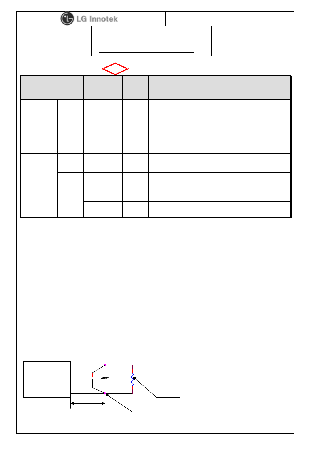
As shown in fig.1 C1(47uF) electrolytic
capacitor and C2 (0.1uF) film capacitor
PSU
C2
+
C1
-
shall be connected between measuring
Load
points when measuring ripple noise.
Fig 1
100mm
Measuring Point
(30)-4022
Page 6
DOCUMENT No : 11(개A)EP-070
S P E C I F I C A T I O N
MODEL NAME : PSPI-L103A .
3. Environment Requirement
Operating Temperature Range 0 to 70 deg.
Operating Humidity Range 20 to 80 %
Storage Temperature Range -20 to 70 deg.
Storage Humidity Range 10 to 90 %
MTBF
Mean Time Between Failure
Cooling Condition Natural Air
98
㎨
Shock test consists of pivoting the power supply, from one
Shock
edge of it’s bottom side, on a flat surface (such as wood
having thickness of 10mm or more) and allowing the
opposite edge to fall from a height of 50mm to this surface.
The test is performed three times on each edge of the
bottom side of the power supply
440,000hour(Tool_Telcordia Issue 1)
REV.NO : 0.1
PAGE :
4
Under Development Mass Product
Frequency (Hz) 2~200 2~200
Vibration
Acceleration
(Grms)
Time (min) 20 min. /
Direction X, Y, Z
1.04 0.84
축
4. Dielectric Strength Voltage
① Live & Neutral to all Secondary(+ line) : 3.0KVac or 4242Vdc
Dielectric
Strength Voltage
※ Above tests are performed at room temperature in non-condensing atmospheric conditions
※ Frame grounds are connected to secondary circuits.
※ Cut OFF condition : 10mA
for 1 Minute
② Live & Neutral to all Secondary GND : 1.5KVac or 2121Vdc
for 1 Minute.
※ 1.8KVac for 1 seconds (Mass Production)
5. Insulation Resistance
Insulation
Resistance
Insulation resistance shall be 8MΩ
between primary Live, Neutral line and secondary.
~ ∞Ωat 500Vdc after 60sec.
(30)-4022
Page 7
DOCUMENT No : 11(개A)EP-070
S P E C I F I C A T I O N
MODEL NAME : PSPI-L103A .
6. Burn – in(1h)
AC 110V Input Voltage, Nominal Load, ambient temperature 45℃±5
-
MP 1'st : 24 Hr
MP ~ 2.0 K : 12 Hr
2.0 ~ 5.0 K : 8 Hr
After 5.0 K : 1 Hr ( According to below condition. *note1)
when operating 1Hr Aging, The condition of ELT(양산보증시험) Aging is same
※
as note2 and be tested following note2.
Also result should be written on the forwarding report (출하성적서).
※ 1 Hours Standard (*note1)
Start
30min
AC
Off
/On
REV.NO : 0.1
PAGE :
5
Discharge for 5min.
1h
AC
Off
/On
/Off
Check [30min 간격 이상유무 확인]
* When happened a fault on check process for 30 min intervals and On/Off test ,
Serial No., fault phenomenon and time from Aging start to fault happening are record ed.
※ note2
비고Spec.
구분
구분
시간
시간
On/Off Test
On/Off Test
60 ℃ (58±2℃)Chamber 온도
60 ℃ (58±2℃)Chamber 온도
양산 품(20hr)
양산 품(20hr)
4M변경 품(44hr)
4M변경 품(44hr)
st
st
품(68hr)
품(68hr)
MP 1
MP 1
시험 종료 시
시험 종료 시
On/Off Test 실시
On/Off Test 실시
비고Spec.
동작온도 승인원 기준고온동작 TestTest 항목
동작온도 승인원 기준고온동작 TestTest 항목
Max 80% load 기준승인원 기준Load
Max 80% load 기준승인원 기준Load
2회이상(AC 전원)
2회이상(AC 전원)
On/Off Time : 각 10s
On/Off Time : 각 10s
Lot size
Lot size
0 ~
0 ~
1,000
1,000
1,001 ~
1,001 ~
2,000
2,000
2,001 ~
2,001 ~
3,000
3,000
3,001 ~
3,001 ~
4,000
4,000
4,001 ~
4,001 ~
5,000
5,000
5,001 ~
5,001 ~
6,000
6,000
5
5
20 Hrs
20 Hrs
10
10
44 Hrs
44 Hrs
15
15
201510
201510
251510
251510
302015
302015
302015
302015
353020
353020
MP 1st Lot4M 변경품양산 Lot
MP 1st Lot4M 변경품양산 Lot
Time시료 수Time시료 수Time시료 수
Time시료 수Time시료 수Time시료 수
68 Hrs
68 Hrs
(30)-4022
Page 8

DOCUMENT No : 11(개A)EP-070
7. Interface
Signal Description
RL_ON
M_ON
(Module_ON)
AC_DET
5.2V, 17V
ON/OFF
M5V / Vs Va
ON / OFF
Monitor for
AC input voltage
S P E C I F I C A T I O N
MODEL NAME : PSPI-L103A .
Signal
Direction
Input
Input
Output
HIGH : 5.2V, 17V ON
LOW : 5.2V, 17V OFF
HIGH : M5V / Vs,Va ON
LOW : M5V / Vs,Va OFF
HIGH : Active
LOW : Inactive
REV.NO : 0.1
PAGE :
Active Level
6
High : more
than 2V
Low : Less
than 0.7V
High : more
than 3V
Low : Less
than 0.7V
High : more
than 4V
Low : Less
than 0.7V
•Auto Power turn on System
- If VSC B/D is not connected PSU through 18pin connector, auto power
on mode is operated from PDP Set Signal.
8. Product Safety
Safety Standards to be applied
EMI / RFI Standards to be applied
Design to meet the requirements as follows
UL60065 and IEC/EN60065
Design to meet the requirements as follows
FCC and EN55020 Class B
with 4dB minimum margin.
9. Construction
Weight Less than 670g / PSU
Unit Size 196(W) x 245(D) x 27(H)(with PCB)
1.6mm ~ 3.0 mm under
Lead Length
IC102,IC103,IC352,IC902,IC903 are 4.8mm under
D351,Q356 are 5.5mm under
Height
27mm (with PCB)
TH101,C907,C351 and C502 are Max. 27mm
height (without PCB)
RL103 are Max. 27mm+5mm height (without PCB)
T901 are Max. 29mm height (without PCB)
(30)-4022
Page 9

DOCUMENT No : 11(개A)EP-070
S P E C I F I C A T I O N
MODEL NAME : PSPI-L103A .
* Construction _ Height limit exception components
T901
REV.NO : 0.1
PAGE :
7
C907
C502
TH101
C351
RL103
(30)-4022
Page 10

DOCUMENT No : 11(개A)EP-070
MODEL NAME : PSPI-L103A .
10. Function of protection
Protection Output Circuit Trip point Notes
Over Current
Under Voltage
Over Voltage
S P E C I F I C A T I O N
CTQ
STBY 2.5A ~ 20A
5.2V 6A ~ 20A
M5V 4.1A ~ 20A
17V 3.1A ~ 8A
Va 2.1A ~ 12A
Vs 1.5A ~ 6A
5.2V 3.5V ~ 4.5V
M5V 3.5V ~ 4.5V
17V 8V ~ 14V
Va 40V ~ 50V
Vs 165V ~ 180V
5.2V 5.5V ~ 9.0V
M5V 5.5V ~ 7.0V
17V 19.5V ~ 28V
Va 60V ~ 70V
Vs 215V ~ 240V
REV.NO : 0.1
PAGE :
8
Shut down
Shut down
Shut down
Shut down
Hiccup or
※ The OCP test of STBY, 5.2V, M5V and 17V should setup current rise slew rate greater than 3.6A/S.
※ This Power Supply has above-mentioned protections.
※ The time for short shall be less than 10sec.
※ PSU should be shutdown by under voltage protection when short circuit test
※ PSU should be wake up normally when AC off-on / Relay off-on / protection removal
※ Short circuit protection between different output terminals is not considered.
※ Trip point for over voltage indicates the operating point when the output voltage
slowly increases.
※ The conditions of Over Current measurement
부하조건
구분
구분
OCP
OCP
(100Vac)
(100Vac)
출력전압 조정
출력전압 조정
(110Vac)
(110Vac)
측정포
측정포
인트
인트
5.2Vst
M5V 1ANom
17V
17V
Va
Va
Vs
Vs
5.2Vst
Nom
Nom Min
5.2Vsc
Nom
-
-
Nom
Nom
Nom
NOMINAL(42HD/50FHD/60FHD :205V )
-
-
NOMINAL(42
NOMINAL(42
M5V
Nom
Nom
NomNom
-
-
Min
부하조건
17V
17V
1A
1ANomNom5.2Vsc
-
-
”
”
/50FHD/60FHD:55V)
0.3A
0.3A
VsVa
VsVa
0.3A
0.3A
0.1A-MINVa
0.1A-MINVa
-0.01AMINVs
-0.01AMINVs
MINMINMIN전출력OVP (100Vac)
MINMINMIN전출력OVP (100Vac)
MINMINMIN전출력UVP (100Vac)
MINMINMIN전출력UVP (100Vac)
10-1. AC Over-voltage Test
1) Over voltage shall test 315Vac~340Vac , Protection should be occur.
2) No fire, shock hazard or explosion sh all occur.
(30)-4022
Page 11

DOCUMENT No : 11(개A)EP-070
S P E C I F I C A T I O N
MODEL NAME : PSPI-L103A .
11. Input / output Pin Assignment
AC Input
SK101
1 AC
2 AC
Wafer YAW396-02M1
PSU VSC Board
1 17V 2 17V
3 GND 4 GND
5 5V 6 5V
7 5V 8 Error_DET
9 GND 10 GND
11 GND 12 GND
13 STBY 14 STBY
15 RL_ON 16 AC DET
17 M_ON 18 AUTO_GND
Wafer
P813
SMAW200-H18S2
REV.NO : 0.1
PAGE :
9
PSU PDP Module
Pin P811
1 Vs
2 Vs
3 NC
4 GND
5 GND
6 Va
7 M5V
Wafer YAW396-H73FD
SK101
2 1
7~15 mm
7 6 5 4 3 2 1
P811
P813
18 2
7~15mm
(30)-4022
Page 12

DOCUMENT No : 11(개A)EP-070
12. Power Sequence
AC IN
AC_DET
5V
STBY5.2V
RL_ON
M_ON
5.2V,17V
S P E C I F I C A T I O N
MODEL NAME : PSPI-L103A .
90%
Max. 150ms
AC-OFF
REV.NO : 0.1
PAGE :
10
DC-OFF
3.5V
90%
M5V
Va
Vs
Max. 150ms
Ton
Min. 200ms
Max.300ms
10%
10%
90%
Min 50ms / Max 200ms
90%
Min 50ms / Max 200ms
Toff
90%
10%
Min.2000ms
※ * RL_ON, M_ON signal is come from VSC B’d, So, Sequence spec related RL_ON,
M_ON is just guide spec for PDP Buyer. Measured data can’t be judged OK or NG.
Va, Vs 전압이 10% 이하 일 경우에만 상기의 Ton , TVaR , TVsR 에 meet 할수있다.
Toff 시간은 AC 전원으로 (플러그 해제) off 한 경우는 제외된다,
※ M_ON은 RL_ON 이후 Max50ms이전에 입력 되었을 경우로 한다
(30)-4022
Page 13

DOCUMENT No : 11(개A)EP-070
13. Block Diagram
AC INPUT(90~264V)
EMI Filter
L/F * 3EA
Relay
250Vac 10A
Rectifier
(600V 15A)
S P E C I F I C A T I O N
MODEL NAME : PSPI-L103A .
STBY
Trans
EER2828
Control IC
STR-
W6052S
MBRB2060CT
10V 3300UF
REV.NO : 0.1
PAGE :
AOD484
25V 1UF
AOD484
10V 470UF
AOD484
16V 100UF
MBRD10200CT
AP9575GS
50V 220UF*2
25V 220UF
11
STBY
5.1V
M5V
17V
Control IC
R2A20112
Multi V Level
Vs V Level
Va V Level
RL On/VS On
EER2820 * 2
TK12A60U * 2
MURF1060CT
450V 120uF * 2
AC Det
PFC
MICOM
MC81F4216D
Control IC
NCP1397B
5V(STBY5V)ON
Va
Multi ON
/Vs ON
PFC ON
Multi1차
Vs/Va Trans
(LLC Resonant)
EER3944
TK12A60D * 2
SDURF1040CTR
F/B
SDURF1040CT
250V 150UF
TK13A25D
MBRF10200CT
80V 330UF
100V 33UF
VS
VA
(30)-4022
Page 14

DOCUMENT No : 11(개A)EP-070
S P E C I F I C A T I O N
MODEL NAME : PSPI-L103A .
14. Electrical characteristics
No. Test Item Test method
1 Intermittent
Operation stability
test
2 Low temperature
operation
3 Low temperature
Storage test
Leave at low
temperature
The switching regulator shall ON-OFF for 20,000 time at an
interval of 10 sec at typical load, after that electrical characteristics
shall be satisfied.
The switching regulator is left at the operating guarantee minimum
temperature for 2 hours without applying electricity.
After that power shall be turned on, and then the electrical
characteristics shall be satisfied.
The switching regulator is left at minimum storage temperature for
96 hours or more.
Then the switching regulator is left at a room temperature and
humidity for 1hour or more, after that electrical characteristics shall
be satisfied.
REV.NO : 0.1
PAGE :
12
4 Heat cycle storage
test
The switching regulator is 10 consecutive temperature cycle that
shown below is performed and then leave them at room temperature
and humidity for 1 hour or more.
After that, electrical characteristics shall be satisfied.
Time Temperature
30 minutes 25℃
30 minutes 25 ℃→-20 ℃
60 minutes Minimum storage temperature(-20 ℃)
30 minutes -20 ℃→25 ℃
30 minutes 25 ℃
30 minutes 25 ℃→70 ℃
60 minutes Maximum storage temperature (70 ℃)
30 minutes 70 ℃→25 ℃
(30)-4022
Page 15

DOCUMENT No : 11(개A)EP-070
S P E C I F I C A T I O N
MODEL NAME : PSPI-L103A .
No. Test Item Test method
5 Heat shock Test Heat shock test performed under following conditions without
applying electricity and then leave them at room temperature and
humidity for 1hour or more.
After that, electrical characteristics shall be satisfied.
Condition : -20℃(120minutes), 70℃(120 minutes),
Switching time : 4minutes(±1minutes), 10 cycle
REV.NO : 0.1
PAGE :
13
15. Mechanical characteristics
No. Test Item Test method
1 Appearance There shall be no contaminant or dirt on the switching regulator
which has adverse effect on electrical characteristics.
There shall be no excessive unevenness or scratches on the plated
or painted surface.
2 Vibration
Frequency
(Hz)
Acceleration
(Grms)
Time (min) 20 min. /
Direction X, Y, Z
After that electrical characteristics shall be satisfied.
There shall be no damage to appearance and construction.
3 Shock Shock : 98m/s^2
On the oak more than 10mm thickness with the flat face, raise the
one side for 50mm, and it carries out each side free fall for three
sides.
There shall be no damage to appearance and construction.
Under Development Mass Product
2~200 2~200
1.04 0.84
축
(30)-4022
Page 16

DOCUMENT No : 11(개A)EP-070
S P E C I F I C A T I O N
MODEL NAME : PSPI-L103A .
16. Sound noise characteristics
PSU NOISE MEASURE POINT
PSU NOISE MEASURE POINT
PSU NOISE MEASURE POINT
PSU
★ ★ ★
CTQ
at a distance of 60
cm to noise source
REV.NO : 0.1
PAGE :
14
4189 mic
anechoic room 內
PSU NOISE SPEC.
PSU NOISE SPEC.
PSU NOISE SPEC.
22.5dB(A) /20.0u Pa2.00E-5 Pa
Each Frequency
(1/1 octave, A-weighting, to 1khz~16khz Total overall)
Measure Location : Anechoic Room
Measure Condition : at a distance of 60 cm to mic.
full white pattern, at AC 110V/220V
The Max Specification : measure 3 points,
at PSU center and left & right on the outside..
17. Micom Definitions
V0.06A-2478
F4216D
YYWW
※ Version : V0.06A
Checksum : 2478
(30)-4022
Page 17

DOCUMENT No : 11(개A)EP-070
MODEL NAME : PSPI-L103A .
18. Bar code Specification
2~3mm
8 mm
LB81E626097010001(0.1)
LB81E626097010001(0.1)
S P E C I F I C A T I O N
40 mm min
34mm min
REV.NO : 0.1
PAGE :
2~3mm
5mm min
Label Form
15
※
Bar Code Size는
그림의
size보다
Manufacturing code
Manufacturing Year
Manufacturing Month
Manufacturing Date
Manufacturing Line
LG Part No.
Serial. No.
Approval sheet
Version
그림의
줄일수는
size가
최소size이며, 업체
없음.
기준및PCB공간에
L (L : LGIT)
B (9:2009,A:2010,B:2011,…)
8 (1,2,3,… 10:O, 11:N, 12:D)
1 (1~9, … A:10, B:11, C:12, … X)
A~D : Gwangju
E~N or 0~9 : Yantai(china)
62609701 (EAY62609701)
0001 (10Digit, 0001~9999)
(0.1)
따라
변경할수
I,O Except
있으나,
RemarkBarcode SpecificationCode
Barcode type : 93 code
Barcode length : 17 digit
Label size : 8 X 36 mm (minimize)
※ BARCODE PRINTING : DO NOT ERASE, WHEN RUB BY HAND.
(30)-4022
Page 18

DOCUMENT No : 11(개A)EP-070
Ⅲ.SCHEMATIC
※ APPENDIX 참고
S P E C I F I C A T I O N
MODEL NAME : PSPI-L103A.
REV.NO : 0.1
PAGE :
16
Page 19

DOCUMENT No : 11(개A)EP-070
※ APPENDIX 참고
S P E C I F I C A T I O N
MODEL NAME : PSPI-L103A.
REV.NO : 0.1
PAGE :
17
Page 20

DOCUMENT No : 11(개A)EP-070
※ APPENDIX 참고
S P E C I F I C A T I O N
MODEL NAME : PSPI-L103A.
REV.NO : 0.1
PAGE :
18
Page 21

5V_MI
C731
0.47uF
D601
Q706
C
B
C724
E
2SD2114KW
D702
1N4148W
RL103
50V
DG5D1-0-2
4
3
0.1uF
R742
4.7K5%1/8W
R746
4.7K
1/8W
RL2
5%
30PDA60-FA7
D602
MURF1060CT
A1
A2
C
2
1
1/4W1%620K
1/4W1%620K
1/4W1%620K
R106
150K
1/8W
LF101
50uH
CY104
330pF
CY105
1%
Q605
KTD1347
C
15V
ZD601
R10 3
240 K
1/8 W
E
B
D60 8
1N4 148 W
D307
GPP10J-E3
600V
C311
0.1uF
50V
1%
C625
0.1uF
330pF
50V
VCC2
LF104
50uH
R105
R10 4
150K
240 K
1/8W
1/8 W
1%
1%
D609
1N4007
VCC1
R628
2.7K
1/8W
5%
C312
2200pF
1KV
D/ST
1
VCC
4
C307
33uF
50V
NXB
YAW396-02M
SK101
5V_MI
AC_DET
PFC_ON
T10A H -250V
F101
2
1
R631
1K
1/8W
5%
4
3
1
2
MULTI_INPUT
VA1 01
IC102
PC-17K1C
IC103
PC-17K1C
12mH
LF102
INR 14D 62 1K- AM OTE CH
VCC2
R125
1
R124
2
4
3
1 2
10K
1.8K
1/8W
1/8W
D304
5%
5%
SB140A
34
40V
R3052W5%
0.33
IC101
KIA431BM
C108
R101
R102
R108
R107
150K
1/8W
1%
50V
IC301
STR-W6052S
3
S/OCP
BR
7
GND
5
6
FB/OLP
10V
ZD303
CY1 03
100 0pF
250 V
CX106
0.47uF
275V
CY1 02
100 0pF
250 V
C112
R119
51K
1/8W
R120
91K
1%
0.01uF
1%
1/8W
C309
2200pF
50V
0.15uF
K
R
C113
A
0.047uF
50V
C301
0.1uF
50V
THE SYMBOL MARK OF THIS SCHEMETIC DIAGRAM INCORPORATES
SPECIAL FEATURES IMPORTANT FOR PROTECTION FROM X-RADIATION.
FILRE AND ELECTRICAL SHOCK HAZARDS, WHEN SERVICING IF IS
ESSENTIAL THAT ONLY MANUFATURES SPECFIED PARTS BE USED FOR
THE CRITICAL COMPONENTS IN THE SYMBOL MARK OF THE SCHEMETIC.
R301
75K2W5%
D10 3
C303
100uF
50V
LXV
1KV
1N4 007
VCC
D305
1N4007
1KV
R307
10K
1
P101
ZD301
15V
KTC3198-Y
5%
1/8W
ZD302
TH101
15-ohm
VCC1
Q301
132
18V
P102
R304
1/8W
1%
1/8W
17V
3.0A
C356
1uF
25V
STBY_ON
C363
470uF
10V
NXB
6.3 X11
31
R615
R616
R617
R618
1.2M
1.2M
68K
51K
STBY
2.0A
1/2W
1/2W
3.0A
1/8W
1/8W
5V
PFC
1%1%
1%
1%
5
3
2
1
L60 1
EE2 820
6
8
10
1
A
1KV
D303
UF4007
5%
10K
1/8W
C308
100uF
50V
LXV
C302
1000pF
50V
AC1
2
4
3
AC2
1
3
5 8
6
4
3
D101
D15XB60-7000
C
1
T301
EER2828
IC352
PC-17K1C
C601
1uF
500V
R624
33K
1/8W
1%
R632
3M
1/8W
5%
C619
C352
R
R358
R360
18
1W
5%
0.1uF
OPEN
C
50V
C607
220pF
50V
R353
4.7K
1/8W
1
C351
3300uF
10V
NXB
R385
OPEN
C373
OPEN
1%
R627
33K
1/8W
1%
P301
P302
OPEN
R626
51K
P304
1
P307
1
1
1
P310
1%
R354
18K
1/8W
R359
12K
1/8W
1%
1%
R356
10K
1/8W
C608
C624
0.1uF
2.2uF
12
11
10
9
1
2
R351
R352
50V
50V
D352
MBRD10U200CT
A1
A2
C368
680pF
2KV
P3051P306
D351
MBRS2060CT
A2
C
A1
C362
330pF
2KV
390
1/8W
1%
K
IC351
A
1.8K
1/8W
5%
KIA2431AS
1
R366
470
1/8W
1%
C358
OPEN
C606
0.47uF
50V
1/8W
P311
R601
33K
1/8W
1%
C605
1/8W1%
R625
680K
0.47uF
50V
1%
1
5V_MI
C
E
Q358
KRC103S
B
C365
220uF
50V
NXB
C354
0.1uF
50V
ZCD-M
ZCD-S
TM
VREF
SGND
RAMP
RT
COMP
R361
100K
1/8W
5%
STBY_SAVE
5
6
IC601
R2A20112ASP
1
2
3
4
5
6
7
8
R367
7.5K5%1/8W
5%
R368
7.5K
1/8W
C377
220uF
50V
NXB
C355
0.1uF
50V
Q357
2SA1504S
C369
2200pF
50V
Q352
AP40T03GH
D
G
Q353
AP40T03GH
D
G
B
16
15
14
13
12
11
10
9
C375
0.1uF
50V
3
8
S
S
C
E
VCC
GD-M
PGND
GD-S
OCP-M
OCP-S
SS
FB
E
C
C372
OPEN
ZD352
2
1
10
D603
1N4148W
6.8
R610
R369
KTC3875SY(ALY)
16V
Q362
KRC103S
B
ZD353
16V
5%
1/8W
C613
0.47uF
50V
39K
1/8W
L60 2
EE2 820
R605
5%
R381
C
E
200
Q359
100K
5%
1/8W
R623
220
Q356
AP9575GS
S
13K
R373
C
E
1/8W
5%
Q363
KRC103S
B
Q603
TK12A60U
D
G
S
1
B
C610
1uF
25V
R380
4.7K5%1/8W
C
E
P308
C359
0.1uF
50V
Q367
KRC103S
1
MULTI_ON
R379
4.7K
1/8W
5%
B
D604
1N4148W
6.8
R606
C611
50V
100uF
LXV
MULTI_ON
C379
0.1uF
50V
1/8W
5%
P309
M5V_ON
1/8W
C612
2200pF
50V
G
1/8W
C357
0.1uF
50V
R603
1%
5%
R382
68K
B
47K
1/8W
C623
0.47uF
50V
D
C361
0.1uF
50V
R370
47K
C
E
1/8W
C374
0.1uF
50V
5%
R60 75W5%
0.035
P303
5%
1/8W
Q364
KRC103S
5%
U-Power 50"PV1
R604
200
5%
1/8W
R622
1
KTC3875SY(ALY)
D
TK12A60U
R608
220
C615
2200pF
50V
R374
G
6.3 X11
Q601
G
68K
5%
1/8W
1/8W
1%
10K
5%
1/8W
6.8 V
Q35 1
AP4 0T0 3G H
S
ZD354
C370
0.1uF
50V
C364
470uF
10V
NXB
R61 35W5%
Q360
ZD3 51
16V
D
S
0.035
VCC
C
E
R357
M5V
2.5A
C366
0.022uF
B
MMSD4148T1G
100K
1/8W
Q366
C
KRC103S
E
5%
C617
450V
D353
100V
B
C618
120uF
120uF
450V
C620
2200pF
50V
R376
5.6K
1%
1/8W
1%
R377
1.2K
R375
50V
270K
1/8W
R383
1/8W
5%
R378
5.1K
1/8W
1%
47K
5%
1/8W
Q365
C
KRC103S
B
C367
0.1uF
50V
C378
E
0.1uF
50V
2011. 09. 03
R620
15K
R6211K1%
C371
220uF
25V
NXB
PFC/STBY/Multi
Page 22

5V_MI
R718
30
1/8W
5%
5.1V
ZD704
C701
100uF
16V
NXB
6.3 X11
M5V
M5V_ON
MULTI_ON
PFC_ON
AC_DET
VS_ON
RL2
STBY_SAVE
STBY_ON
R757
2.7K
1/10W
R728
390
1/10W
5%
1%
R725
1K
1/10W
5%
R750
1K
1/10W
5%
R751
4.7K
5%
1/10W
R726
10K
1/10W
R752
5%
4.7K
5%
1/10W
6
5
R753
1K
1/10W
5%
4
25036WS-06B
EC1/SCK/EXT2/AN2/R04
PWM1O/T1O/SI/EXT3/AN3/R05
EC2/SO/EXT4/AN4/R06
[SDATA]T2O/EXT5/AN5/R07
VREF/EXT6/R10
[SCLK]PWM2O/EXT7/AN6/R11
RXD/R14
TXD/R15
AN10/R25
VDD
IC701
MC81F4216D
1
2
3
4
5
6
7
8
9
10
R03/AN1/EXT1/T0O/PWM0O
20
R02/AN0/EXT0/EC0
19
SXOUT/R01/EXT11
18
SXIN/R00/EXT10
17
VSS
16
RESETB/R35/VPP
15
14
13
12
11
XIN/R34
XOUT/R33
R27/AN12
R26/AN11
R736
1/10W
10K
5%
R733
100K
5%
1/10W
R760
22K
1/10W
1%
10K
1/10W
Q702
2SC3875S(ALY)
C
B
E
R732
R731
20K
1/10W
1000pF
R777
1K
1/10W
5%
50V
5%
5%
47K
1/10W
C713
R722
1K
1/10W
5%
R719
220K
M_ON_IN
VS_DET
1/10W
5%
AUTO_GND
AC_ON
VA_DET
ERROR_DET
R734
2.2K
C714
1/10W
50V
1000pF
5%
R735
R723
5.6K
1/10W
1%
D710
MMSB414B
D704
MMSB414B
R737
220K
1/10W
5%
5%
P701
1
2
3
17V
5V
STBY
RL_ON
M_ON_IN
R727
47K
1/10W
5%
C715
1000pF
SMAW200-H18T-S
17V
1
GND
3
5V
5
5V
7
GND
9
GND
11
STBY
13
15
M_ON
17
50V
P813
2
4
6
8
10
12
14
16
18
C708
17V
GND
5V
ERROR_DET
GND
GND
STBY
AC_ONRL_ON
AUTO_GND
50V
0.1uF
R758
2.7K
C716
0.1uF
50V
1%
1/10W
17V
5V
ERROR_DET
STBY
AC_ON
AUTO_GND
P811
YAW396-H73FD
1
VS
2
VS
NC
4
GND
5
GND
6
VA
7
M5V
8
VA
M5V
C750
0.1uF
50V
0.022uF
5V
17V
ZD702
24V
50V
R748
100
1/10W
5%
ZD703
7.5V
C741
0.1uF
50V
R747
100
C702
1/10W
5%
R740
10K
50V
1000pF
R755
5.6K
R745
10K
1/10W
5%
5%
1/10W
1%
R756
5.1K
1/10W
1/10W
R741
10K
1/10W
1%
R743
18K
1/10W
1%
Q703
2SC3875S(ALY)
C
B
E
C755
1%
50V
1000pF
R713
R744
1.6K
1%
R724
5.1K
5.6K
1N4148W_DIODES
1/10W
1/10W
1%
1/10W
D703
1%
R739
5.6K
1/10W
1%
C778
50V
1000pF
R717
2.2K
1/10W
5%
R714
100K
1/10W
5%
R712
10K
1/10W
5%
Q701
C
2SC3875S(ALY)
B
E
R738
VA701
Chip Varistor
R701
RL_ON
20K
1/10W
C712
5%
50V
1000pF
5%
47K
1/10W
C710
VS
THE SYMBOL MARK OF THIS SCHEMETIC DIAGRAM INCORPORATES
SPECIAL FEATURES IMPORTANT FOR PROTECTION FROM X-RADIATION.
FILRE AND ELECTRICAL SHOCK HAZARDS, WHEN SERVICING IF IS
ESSENTIAL THAT ONLY MANUFATURES SPECFIED PARTS BE USED FOR
THE CRITICAL COMPONENTS IN THE SYMBOL MARK OF THE SCHEMETIC.
2011. 09. 03U-Power 50"PV1
2 3Micom
Page 23

MULTI_INPUT
F801
T4A H-250V
PFC
D805
MUR160RLG
600V
5%
R823
10
ZD803
1/8W
15V
C813
0.1uF
50V
VCC
14HB15
3
4
RT
CTIMER
1%
330
R833
1/8W
C818
22uF
50V
1/8W 1%
1%
R812
11K
1/8W
R831
6.8K5%1/8W
1.2K
R816
1/8W
1%
R828
IC801
1.2K
NCP1397
R820
10K
1%
1/8W
C809
22uF
50V
VBOOT
16
1
CSS[DIS]
1/8W
1%
R818
R819
6800
1/8W
1%
MUPPER
2
FMAX
1M
12
RB160M-30
GND11MLOWER
10
6FB5BO7DT8
R825
4.7K
1/8W
1%
R824821/8W
C807
330nF
50V
D801
R801
51
1/8W
5%
RB160M-30
R803
51
1/8W
5%
C808
0.1uF
50V
FAULT
9
SKIP/DISABLE
C811
0.47uF
50V
1%
820
R830
D802
1/8W
D
Q801
G
TK12A60D
S
5%
R802
20K
1/8W
D
R8051M1/2W
R806
2.2
1/2W
5%
1/8W
5%
C802
0.022uF
1250V
VCC
C804
10uF
50V
1%
R810
D803
16
C820
270pF
2KV
MMSD4148T1G
R838
8.2K
1/8W
5%
C815
0.01uF
50V
C806
0.068uF
50V
1/8W 1%
R807
1001W5%
D804
MMSD4148T1G
R815
100K
1/8W
5%
R839
IC802
KIA431BM
1K
1/8W
K
A
Q802
G
TK12A60D
S
5%
R804
20K
1/8W
VCC3
C810
0.01uF
50V
C803
10uF
50V
C825
0.1uF
50V
R808
47K
1/8W
5%
C805
R809
10K
1/8W
1%
OPEN
15V
ZD804
R826
20K
C826
1uF
25V
1%
5%
R
C824
0.1uF
50V
T901
EER3944_50T4R4
1
2
3
4
5
6
7
8 9
R844
1.2M
R843
1.2M
R842
150K
R841
150K
C823
0.1uF
50V
R840
15K
1/2W
1/2W
1/8W
1/8W
1/8W
A1
C
1/8W
1/8W
A2
FCF 10A 40
1%
1%
D90 1
C
C506
22uF
100V
VSFB_PC
VR901
20K
R901
R902
R903
R904
R905
R906
47K
47K
47K
33K
33K
2.7K
C502
330uF
80V
1/8W
1/8W
1/8W
1/8W
1/8W
1/8W
1%
1/8W
C903
0.022uF
400V
R909
1K
1/8W
5%
C904
OPEN
R512
24K
1/8W
VSFB_PC
C907
150uF
250V
C905
0.1uF
50V
R
ZD501
22V
R515
24K
1/8W
5%
C507
0.1uF
50V
K
A
R511
5%
56K
IC901
R507
5.1K
1/8W
B
KIA431
1/4W
5%
5%
C
Q504
KRC103S
E
C908
OPEN
Q501
2SK2508
SGD
47K
R51 7
1N4148W_DIODES
D508
ZD503
5%
R501
33K
1/8W
C
KTC3207
Q502
E
ZD502
7.5V
5%
1/8 W
2
15V
B
D506
1N4148W
R516
6.8K5%1/8W
C505
100pF
3
Q503
KTC3198-Y
1
D507
1N4148W_DIODES
R504
C501
100V
10nF
150K
1/8W
1%
R510
820
1/8W
1%
R502
27K
1%
1/8W
50V
R503
8.2K
1/8W
1%
10K
VR502
R505
27K
1%
R506
9.1K
1/8W
1/8W
1%
R9081K1%
1%
1%
1%
1%
R907
1K
1/8W
1%
1%
100K
TH501
1%
R518
39K
1/8W
R519
36K
1/8W
1%
1%
1/8W
R520
1.3K
R918
39K
1/8W
1%
C503
33uF
100V
R919
33K
1/8W
1%
R920
33K
1/8W
1%
R921
33K
1/8W
1%
R514
1/8W
R922
33K
VS_DET
1/8W
1%
R513
24K
1%
1/8W
24K
1%
16
15
14
13
12
11
10
IC902
PC-17K1C
4
3
MULTI_INPUT
1%
1%
1%
1%
1%
VCC3
R827
2.7K1%1/8W
4
3
IC903
PC-17K1C
1
2
D902
FRF10A40
D509
1KV
UF4007
D504
FMX-22S(SP)
A2
A1
R917
STBY
1K
1/8W
5%
VS_ON
17V
R910
6800
1
R911
2
1.2K
203V 1.4A
VA
55V 2.0A
VA_DET
VS
THE SYMBOL MARK OF THIS SCHEMETIC DIAGRAM INCORPORATES
SPECIAL FEATURES IMPORTANT FOR PROTECTION FROM X-RADIATION.
FILRE AND ELECTRICAL SHOCK HAZARDS, WHEN SERVICING IF IS
ESSENTIAL THAT ONLY MANUFATURES SPECFIED PARTS BE USED FOR
THE CRITICAL COMPONENTS IN THE SYMBOL MARK OF THE SCHEMETIC.
CY999
680pF
250V
2011. 09. 03U-Power 50"PV1
3
3VS/VA
 Loading...