

Page 1
SAFETY PRECAUTIONS
SERVICE WARNING
Only qualified service technicians who are familiar with safety checks and
guidelines should perform service work. Before replacing parts, disconnect power source to protect electrostatically sensitive parts. Do not
attempt to modify any circuit unless so recommended by the manufacturer. When servicing the receiver, use an isolation transformer between
the line cord and power receptacle.
GENERAL GUIDELINES
Perform a final SAFETY CHECK before returning receiver to customer.
Check repaired area for poorly soldered connections, and check entire
circuit board for solder splashes. Check board wiring for pinched wires or
wires contacting any high wattage resistors. Check that all control knobs,
shields, covers, grounds, and mounting hardware have been replaced. Be
sure to replace all insulators and restore proper lead dress.
SAFETY CHECKS FIRE AND SHOCK HAZARD
Cold Leakage Checks for Receivers with Isolated Ground
Unplug the AC cord, connect a jumper across the plug prongs, and turn
the power switch on (if applicable). Use an ohmmeter to measure the
resistance between the jumped AC plug and any exposed metal cabinet
parts such as antenna screw heads, control shafts, or handle brackets.
Exposed metal parts with a return path should measure between 1M ohms
and 5.2M ohms. Parts without a return path must measure infinity.
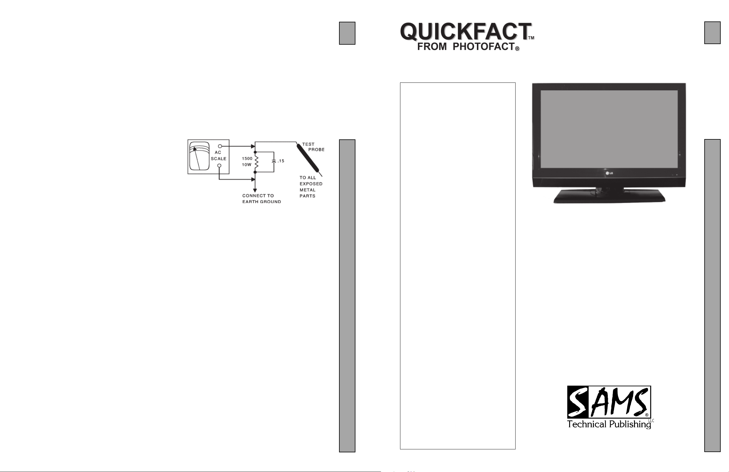
Hot Leakage Current Check
Plug the AC cord directly into an AC outlet. DO NOT use an isolation transformer. Use a 1500 ohms, 10W resistor in parallel with a .15µF capacitor to
connect between any exposed metal parts on the receiver and a good earth
ground. (See figure below.) Use an AC voltmeter with at least 5000 ohms per volt
sensitivity to measure the voltage across the resistor. Check all exposed metal
parts and measure voltage at each point. Voltage measurements should not
exceed .75VAC, 500µA. Any value exceeding this limit constitutes a potential
shock hazard and must be corrected. If the AC plug is not polarized, reverse the
AC plug and repeat exposed metal part voltage measurement at each point.
5388
LCD SERIES
SET 5388
GridTrace Location
Miscellaneous Adjustments ...................... 2
Parts List ................................................... 1
Placement Chart (Resistances) ................. 3
Placement Chart (Voltages) ...................... 3
Safety Precautions .................................... 1
Schematic Component Location .............. 2
Schematic Notes ....................................... 2
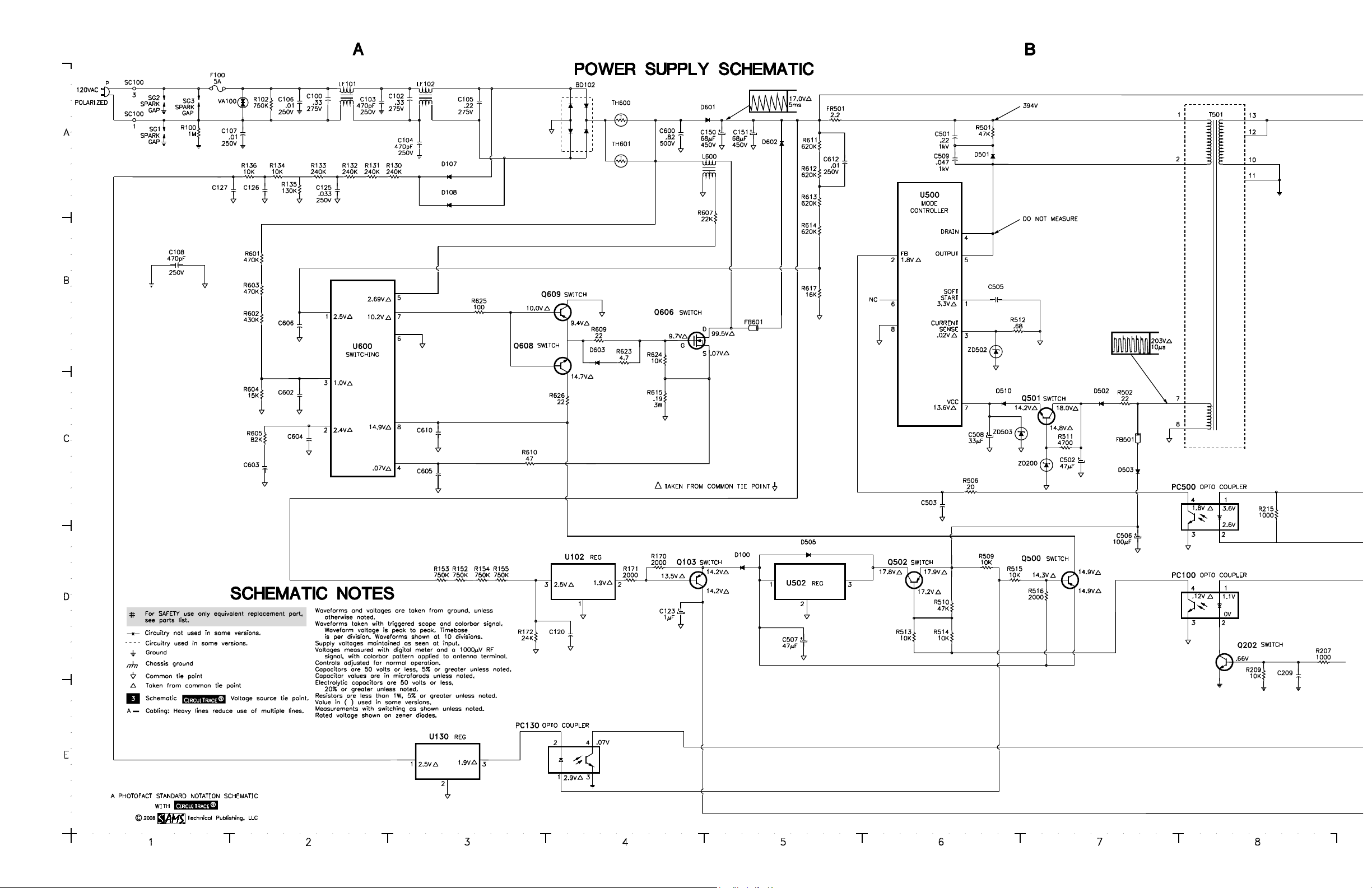
Schematics
LCD SERIES
INDEXINDEX
INDEX
INDEXINDEX
Power Supply .................................... 1
Power Supply Schematic ................... 2
5388
Technical Service Data
LG
MODEL 32LC7D (CHASSIS LA73E)
5388
1
The listing of any available replacement part herein in no case constitutes a recommendation, warranty, or guarantee by
SAMS Technical Publishing, LLC as to the quality and suitability of such replacement part. The numbers of the listed parts have
been compiled from information furnished to SAMS Technical Publishing, LLC by the manufacturers of the specific type of
replacement part listed.
Reproduction or use, without express permission, of editorial or pictorial content, in any manner, is prohibited. No patent
liability is assumed with respect to the use of the information contained herein.
© 2008 SAMS Technical Publishing, LLC
9850 E. 30th St.
Indianapolis IN 46229
www.samswebsite.com
MODEL 32LC7D (CHASSIS LA73E)
THIS IS A GREEN PRODUCT
Do not use lead based solder for repair. Use only
green product parts for replacement.
Essential coverage
for servicing an LCD receiver...
Power Supply Schematic
Miscellaneous adjustments
Placement chart
Parts list
Coverage includes these additional MODELS:
MODELS CHASSIS
32LC7D-UB LA73E
32LC7DC LA73E
32LC7DC-UB LA73E
Printed in the United States of America 5 4 3 2 1 08FP06006
Page 1 SET 5388
!IBCGC|05388X
For a Complete List of Manuals,
Visit www.samswebsite.com
JULY 2008 SET 5388
LG
Page 2

Page 1 SET 5388
PARTS LIST
Item No. Type No. Mfr. Part No. Notes
BD102 D3SBA60 - -
D100 BAV70WT1 - A4
D101 BAV70WT1 - A4
D102 BAV70WT1 - A4
D104 BAV70WT1 - A4
D105 BAV70WT1 - A4
D106 BAV70WT1 - A4
D107 705S1J - -
D108 705S1J - -
D202 MBRF10100CT - -
D203 MBRD20150CT - -
D204 MBRF10100CT - -
D205 MBRD20150CT - -
D207 MBRF1060CT - -
D209 MBRF1060CT - -
D213 1N4148WS - T4 U3
D214 1N4148WS - T4 U3
D215 1N4148WS - T4 U3
D243 1N4148WS - T4 U3
D501 UF4007 - -
D502 UF1007 - -
D503 UF1007 - -
D505 1N4148WS - T4 U3
D510 1N4148WS - T4 U3
D601 S3V 60 - -
D602 FSU10A60 - -
D603 1N4148WS - T4 U3
PC100 EL817 - -
PC130 EL817 - -
PC150 EL817 - -
PC500 EL817 - -
Q100 MMBT2222AT - 1P
Q101 MMBT2222AT - 1P
Q102 BC850B - 2F
Q103 BC850B - 2F
Q150 STP9NK60Z - -
Q151 STP9NK60Z - -
Q200 BC850B - 2F
Q201 MMBT2222AT - 1P
Q202 MMBT2222AT - 1P
Q204 MMBT2222AT - 1P
Q205 AP62T03GH - -
Q207 AP60T03GH - -
Q500 BC850B - 2F
Q501 MMBT2222AT - 1P
Q502 BC850B - 2F
Q606 STW20NM60 - -
Q608 MMBT2222AT - 1P
Q609 - - SL 2C
U100 001 H26 - -
U101 MIC4428 - -
U102 EA1 - -
U130 EA1 - -
U200 IRU3037GH - -
Item No. Type No. Mfr. Part No. Notes
U202 EA1 - -
U203 EA1 - -
U500 ICE3B1565 - -
U502 KA78L15AZ - -
U600 1D0750 5501A - -
Item No. Function/Rating Mfr. Part No. Notes
C211 .01 1kV - -
F100 Fuse - 5Amp, 250V
FB101 Ferrite Bead - -
FB501 Ferrite Bead - -
FB601 Ferrite Bead - -
L200 - - -
L202 - - -
L203 - - -
L204 - - -
L205 - - -
L206 - - -
L600 Choke - LP-001/SJ0729
LF101 Line Choke - -
LF102 Line Choke - -
T101 SMT - LM-002/SJB-003/SJ/SJ0732
T150 - - DT101
T501 SMT - LS-003/SJ0727
TH600 DSC 15D-15 - -
TH601 DSC 15D-15 - -
VA100 Varistor TVR14621 - -
ZD100 - - WJ
ZD200 1N5245 - -
ZD502 1N5227 - -
ZD503 1N5251 - -
# Display EAJ37543301 LCD
PC Board EBR37277301 Control Key
PC Board EBR38577601 LED
EBR36011401 LED
PC Board (1) EBU38568601 Main
PC Board (2) EBU38099801 Main
# PC Board EAY34795001 Power Supply
EAY36768101 Power Supply
PC Board EBR38575001 Side AV
EBR36010601 Side AV
Power Cord 6410TUW008A AC, Polarized
Remote Control AKB32559904 Assembly
Speakers EAB33496901 8 Ohms, 10W
# For SAFETY use only equivalent replacement part.
(1) Used in MODELS 32LC7D and 32LC7D-UB.
(2) Used in MODELS 32LC7DC and 32LCDC-UB.
Page 3
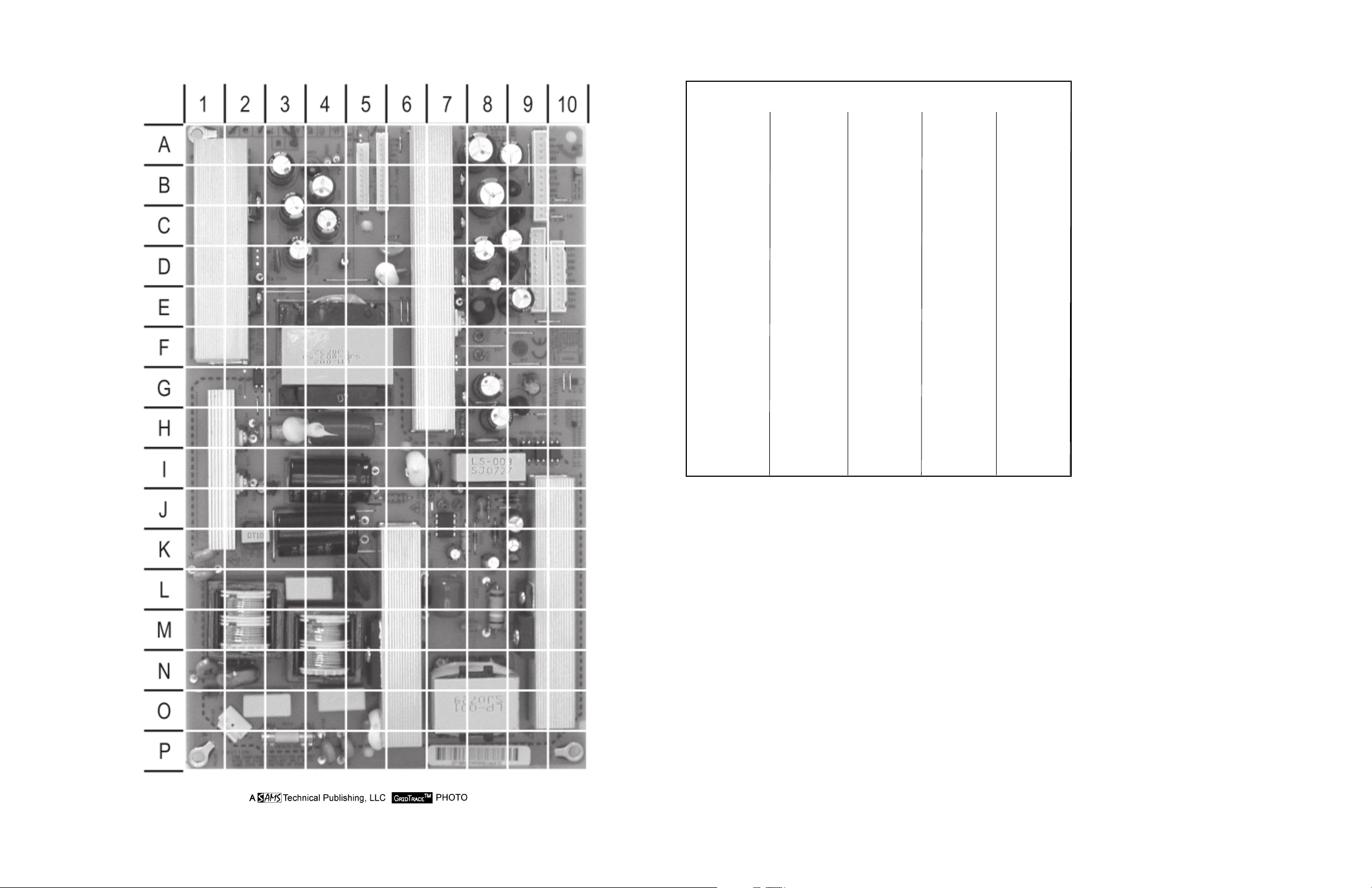
POWER SUPPLY BOARD TOP
POWER SUPPLY BOARD TOP, GRIDTRACE LOCATION GUIDE
SET 5388 Page 1
BD10 M5
C100 O2
C102 L4
C103 L1
C104 P4
C105 O4
C106 P4
C107 N1
C108 K1
C110 H4
C123 I3
C150 J4
C151 I4
C201 D3
C203 B4
C204 H8
C205 G8
C206 C6
C207 A8
C208 A9
C210 D6
C211 G8
C212 B8
C213 C9
C215 D8
C216 D8
C219 D8
C220 G9
C221 B3
C222 A3
C223 D3
C225 E9
C232 C4
C501 I6
C502 K9
C506 J9
C507 K8
C508 K7
C509 I7
C600 L7
C612 M8
D202 G7
D203 B2
D204 B7
D205 E2
D207 C7
D209 D7
D501 I7
D502 K8
D503 J9
D601 L7
D602 L9
F100 P3
FB101 H3
FB501 J8
FB601 L8
FR50 J6
L200 E8
L202 G9
L203 D9
L204 C9
L205 B9
L206 B4
L600 O8
LF101 M2
LF102 M4
P201 A9
P202 D1
P203 D9
PC10 I9
PC13 I1
PC15 G2
PC50 I9
Q150 I2
Q151 H2
Q207 E7
Q606 M9
R100 N1
R102 N2
R151 H3
R202 H7
R206 E7
R208 D5
R210 D4
R211 D2
R253 A4
R254 A4
R501 I6
R502 J8
R512 K7
R615 L8
SC10 O2
T101 F4
T150 K2
T501 I8
TH60 L5
TH60 L5
U500 J7
U502 K9
VA100 N2
ZD20 K9
ZD50 K8
ZD50 K7
Page 4
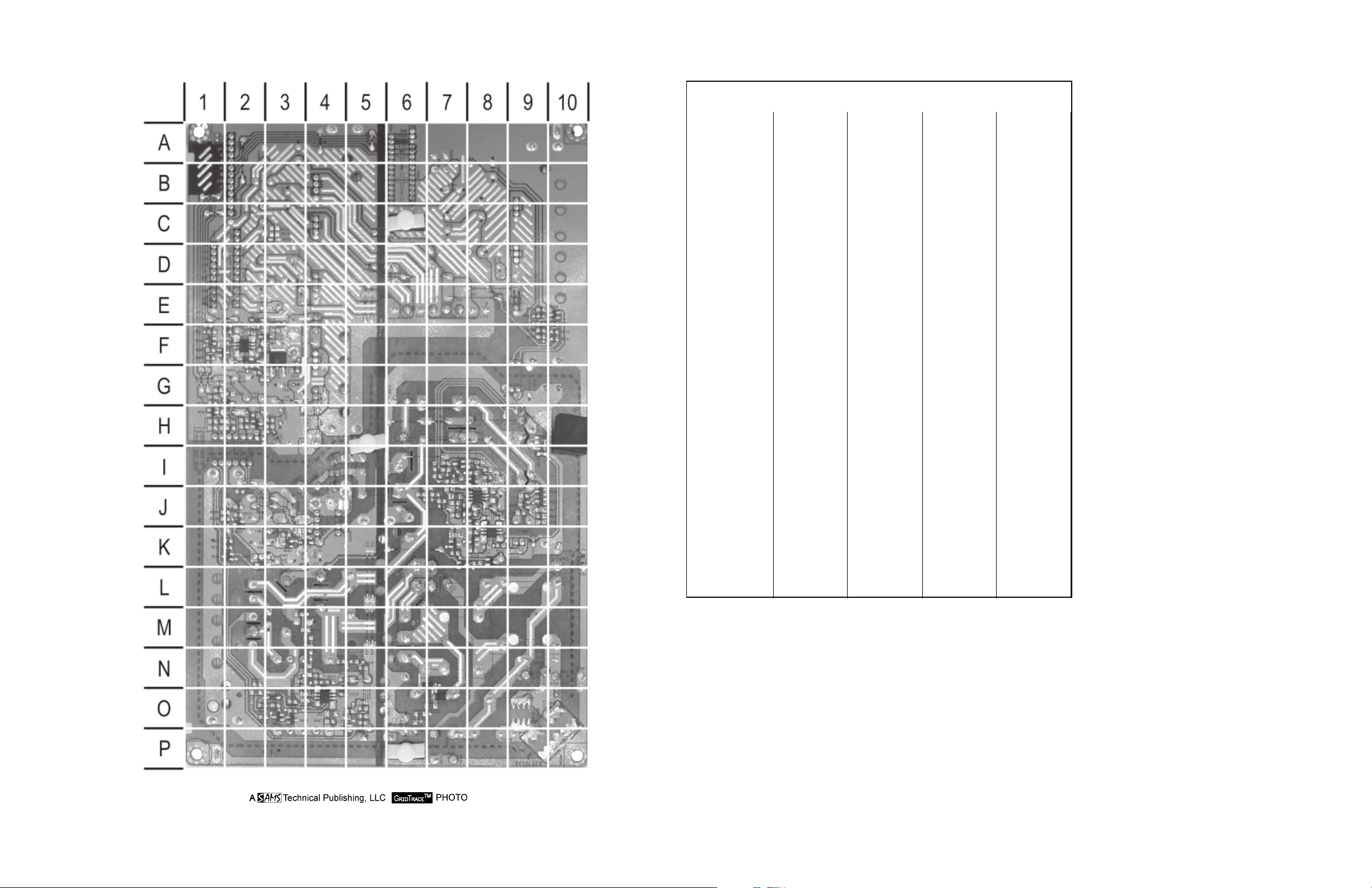
POWER SUPPLY BOARD BOTTOM
POWER SUPPLY BOARD BOTTOM, GRIDTRACE LOCATION GUIDE
C111 J7
C113 J8
C114 K8
C115 K9
C116 J9
C117 J9
C118 J7
C119 J8
C120 K7
C121 I7
C122 I8
C124 I8
C125 O6
C126 O5
C127 O5
C128 K9
C209 G1
C214 H2
C217 H1
C218 G1
C224 F2
C226 F3
C227 F1
C228 F3
C229 G2
C230 F2
C256 E1
C503 K4
C505 K4
C602 N4
C603 N3
C604 O3
C605 O3
C606 N4
C610 O4
D100 K7
D101 J8
D102 K8
D104 H9
D105 J9
D106 J9
D107 O7
D108 N7
D213 E3
D214 E2
D215 F2
D243 F2
D505 K2
D510 K4
D603 O3
Q100 J9
Q101 I8
Q102 I7
Q103 K8
Q200 F1
Q201 H1
Q202 G2
Q204 F1
Q205 F2
Q500 K2
Q501 K3
Q502 J2
Q608 O3
Q609 O3
R101 I9
R109 K8
R130 O7
R131 O6
R132 O6
R133 O5
R134 O5
R135 O5
R136 O5
R137 J8
R152 J7
R153 J6
R154 J7
R155 J7
R156 I8
R157 I7
R158 K8
R160 I9
R161 K8
R162 J9
R163 J9
R164 J9
R165 I7
R167 J7
R168 I7
R169 I8
R170 K8
R171 K7
R172 K7
R173 I8
R201 H2
R207 G1
R209 G2
R213 H3
R214 H2
R215 H2
R216 H3
R217 H2
R218 H2
R221 F10
R222 F10
R223 E9
R225 E9
R226 E9
R227 H1
R228 H1
R229 G1
R230 H1
R235 G3
R236 F1
R237 F1
R238 F1
R239 F1
R240 F2
R241 F2
R244 G2
R245 F2
R247 G3
R249 F9
R250 F9
R506 J2
R509 J2
R510 J2
R511 K3
R513 K2
R514 K2
R515 K2
R516 K2
R601 N4
R602 N5
R603 N5
R604 N4
R605 N3
R607 O4
R609 O3
R610 O3
R611 M3
R612 M4
R613 M4
R614 M4
R617 M4
R623 O3
R624 N2
R625 O3
R626 O2
U100 J8
U101 K8
U102 K7
U130 O5
U200 F2
U202 H2
U203 E1
U600 O4
ZD10 J7
SET 5388 Page 1
Page 5
Page 2 SET 5388
Page 6
SET 5388 Page 2
Page 7

SCHEMATIC COMPONENT LOCATION GUIDE
BD102 A4
C100 A2
C102 A3
C105 A3
C108 B1
C110 B13
C113 E10
C114 E10
C115 D11
C116 E11
C117 E12
C118 C11
C119 D11
C120 D4
C122 C12
C123 D4
C124 C11
C125 A2
C126 A2
C127 A2
C128 E11
C150 A5
C151 A5
C201 B14
C203 B16
C204 A9
C205 A9
C206 D14
C207 D15
C208 D16
C209 D8
C210 D14
C211 E14
C212 C15
C213 C16
C214 C9
C215 C15
C216 C15
C217 E9
C218 E10
C219 C14
C220 B10
C221 B15
C222 B15
C223 B15
C225 A15
C226 A14
C227 B11
C228 A11
C229 A12
C230 A12
C232 B15
C256 D14
C501 A6
C502 C7
C503 C6
C505 B6
C506 D7
C507 D5
C508 C6
C509 A6
C511 D6
C600 A4
C602 C2
C603 C2
C604 C2
C605 C3
C606 B2
C612 A5
CY104 A3
D100 D5
D101 E10
D102 E10
D104 E11
D105 E12
D107 A3
D108 B3
D202 A9
D203 B14
D204 D14
D205 B14
D207 C14
D209 C14
D213 A11
D214 A11
D215 A11
D243 A13
D501 A6
D502 C7
D503 C7
D505 D5
D510 C6
D601 A4
D602 A5
D603 C4
F100 A1
FB101 B12
FB501 C7
FB601 B5
FR501 A5
L200 A14
L202 A10
L203 C15
L204 C15
L205 D15
L206 B15
L600 A4
LF101 A2
LF102 A3
PC100 D8
PC130 E4
PC150 D13
PC500 C8
Q100 E12
Q101 C12
Q102 D11
Q103 D4
Q150 B12
Q151 C12
Q200 B11
Q202 D8
Q204 A15
Q205 A14
Q207 A13
Q207 E9
Q500 D7
Q501 C7
Q502 D6
Q606 B4
Q608 C4
Q609 B4
R100 A1
R101 E11
R102 A2
R107 D4
R109 E10
R131 A2
R132 A2
R133 A2
R134 A2
R135 A2
R136 A2
R137 D11
R151 C12
R152 D3
R153 D3
R154 D3
R155 D3
R156 C12
R157 C12
R158 E10
R160 E11
R161 D11
R162 D11
R165 C12
R165 E12
R167 C11
R168 D11
R169 C11
R171 D4
R172 D3
R173 C11
R178 C11
R202 A9
R201 C9
R206 C14
R207 D8
R208 D14
R209 D8
R210 D14
R211 B14
R213 C10
R214 C9
R215 C8
R216 C10
R217 D9
R218 D10
R221 C14
R222 D14
R223 E14
R227 E9
R228 E9
R229 E10
R230 E9
R235 B13
R236 A15
R237 B15
R238 B11
R240 A14
R241 A13
R242 E14
R243 E14
R244 A12
R244 E14
R245 B14
R247 A14
R249 B15
R250 B15
R253 B16
R254 B16
R501 A6
R502 C7
R506 C6
R509 D6
R510 D6
R511 C7
R512 B6
R513 D6
R514 D6
R515 D6
R515 D7
R516 D7
R601 B2
R602 B2
R603 B2
R604 C2
R605 C2
R607 B5
R608 B4
R610 C3
R612 A5
R613 B5
R614 B5
R615 C4
R616 B5
R617 B5
R623 C4
R624 C4
R625 B3
R626 C4
T101 B13
T150 D11
T501 A8
TH600 A4
TH601 A4
U100 A2
U100 C11
U101 E11
U102 D4
U130 E3
U200 B12
U202 D9
U203 E14
U500 A5
U500 B6
U502 D5
U600 B2
VA100 A2
ZD100 D11
ZD200 C7
ZD502 B6
ZD503 C6
Page 2 SET 5388
PHILIPS MODEL 32PT5441/37 (CHASSIS L04.1UAA)
Page 8

MISCELLANEOUS ADJUSTMENTS
ENTERING THE CALIBRATION MODE
Hold menu key down for approximately 10 seconds
Enter password (8741)
Example screen below
Calibration DTV/AV1/AV2/Component1/Component2/RGB-
PC/ HDMI/DVI /HDMI2/Analog
Pic.Mode Expert1/Expert2
1. Contrast 90
2. Brightness 50
3. Color50
4. Tint 0
5. Sharpness 50
6. R Gain 192
7. G Gain 184
8. B Gain 161
9. R Offset 64
10.G Offset 64
11.B Offset 64
POS/SIZE ADJUST
EZ ADJUST
1. CVBS ACC ADJUST (Unhighlighted)
2. ADC 480i Comp1
3. ADC 1080i Comp1/RGB
4. Reserved (Unhighlighted)
5. Sub-Brightness/Contrast
6. White-Balance
7. Module Control (Unhighlighted)
8. Temperature Threshold (Unhighlighted)
9. White-Pattern
Test Pattern off
W, R, G, B, BLK, Patt (Gray scale)
10. 2 Hour Off Option
11. OAD
The selections that are (Unhighlighted) cannot be selected.
TO ENTER IN-START MODE
(Using the sets remote)
Press menu key on the remote first and the menu key on set second
and hold both for approximately 10 seconds.
(Using the Service Remote Press the IN-START key)
LG MODEL 32LC7D (CHASSIS LA73E)
1. H Position 0
2. V Position 0
3. H Size 0
4. V Size 0
DEFAULT LOAD NO
YES (Sets to factory defaults)
*Count 1
*(How many times calibration mode has been entered)
Exiting hold menu key down for approximately 10 seconds
The Enter password prompt will appear and time out in a few seconds.
TO ENTER EZ ADJUST MODE
(Using the sets remote)
Press menu key on the set first and the menu key on remote second
and hold both for approximately 10 seconds.
(Using the Service Remote Press the adjust key)
IN-START
MODEL : 32LC7D-UB S/W Ver : 03:06 Mic. Ver:
V3.06
UTT : 5 PQ Ver : 02.10.00 PQ MODEL:
32LC7D-UB
COMP 480i : OK COMP 1080i : OK RGB 1080i :
OK
1. MST3361 BANKO (Press Enter on sets remote to
select) (Left or Right arrow to change value)
2. MST3361 BANK1
3. Spread Spectrum Control
4. MODEL Info.
5. Reserved
6. PowerOffStatus
7. BaudRate
8. ADC Adj. Data
9. Reserved
10. Sub B/C Data
11. WB Adj. Data
12. Image Position & Size
The selections that are (Unhighlighted) cannot be selected.
Menu to Exit
PHILIPS MODEL 32PT5441/37 (CHASSIS L04.1UAA)
SET 5388 Page 2
Page 9

Page 3 SET 5388
Page 10

SET 5388 Page 3
Page 11

SET 5388 Page 3Page 3 SET 5388
Page 12

LG MODEL 32LC7D (CHASSIS LA73E)
SET 5388 Page 3
Page 13

YP32DVR Power specification
POWER SPECIFICATION
POWER SPECIFICATION
Page 14

YP32DVR Power specification
1. INTRODUCTION
1.1 Product Description
This specification defines the input, output, performance characteristics, environment, noise
and safety requirements for a LCD power supply.
1.2 Parameter Specification
Unless specification otherwise, all parameters must be met over the limit of temperature
Load, and input volt age.
2. ELECTRICAL REQUIREMENTS
2.1 Input Requirements
AC 100V to AC 240VNominal Input Voltage
Primary Over Current Protection
AC 90V to AC 264VInput Voltage Variation
Under 3.0Arms at 100Vac & load MaxInput Current
50 / 60 HzNominal Frequency
47 Hz to 63 HzFrequency Variation Range
3 Conductors (Live,Neutral,F.G)Configuration
The live line side of the input shall have a fuseInput Fuse
An adequate internal fuse on the AC input line shall be
provided.
Cold start : under 80Ap-p at AC 220Vac(Wall-Out)Inrush Current
Over than 80% at 90Vac & Max loadEfficiency
Over than 0.9 at 100~240Vac & max load conditionPower Factor
Page 15

YP32DVR Power specification
2.2 Output Requirements
2.2.1 Electrical characteristics
SpecificationCONDITIONITEMNO
1
2
3
Output
Voltage
Current (#3)
Current
Load
Inrush
Rating
Tolerance
Cross reg1
Cross reg2
Inrush
Duration
Load MAX
(Refer to #2 MAX)
Load Max (*1)RIPPLE (mV)
1.19V :Variable
2. Other: Max
Test & Aging StandardTOTAL Max.
Off ModeMin-1
ON ModeMin-2
Possible Range
Refer (주 2)
St/by
5V
±5%
150
±5%
±5%
1.5A
0.06A
0.25A
Vo1
3.4V
±5%
150
±5%
0V
5.0A
-
0.05A
Vo2
6V
±5%
(On-Mode
±7%)
180
±5%
0V
3.5A
-
0.05A
Vo3
12V
±5%
350
±5%
0V
1.5A
-
0.05A
Aod
19V
±5%
(On-Mode
±7%)
400
±7%
0V
1.2A
-
0.05A
INV
24V
±7%
480
±5%
0V
4.0A
-
0.05A
Fig 1)
Ripple
Range [A]OCP4
1.Check LINE:
2.Other : Load Max
Range [V]OVP5
1.Check Line:
Yes,NOSCP6
2.Other : Load Max
Switching frequency
Input frequency ( 50 ~ 60Hz)
Vaiable
Short to GND
-
Yes
Yes
-
Yes
Yes
-
Yes
주1) Ripple Test
1-1) Test 방법 : Ripple test는 fig 1을따른다
1-2) Test Point : power output 각 pin
주2) Inrush current
2-1) power가 cover할수있는range를의미함.
2-2) spec over시 voltage dip,부품 dead가능성 있으
므로
명기된 spec 이상 사용하지 말 것.
주3) Load current : 업체 Aging / RQA test standard
* Power On/Off Voltage : 3V ~ 5V
MIN
6.5A
-
Yes
Page 16

YP32DVR Power specification
주4 ) Test Point : power output 각 pin
Add Electrolytic Capacitor 47㎌ + 0.1㎌
700mm
+
Load
Oscilloscope
Measurement point
Power Supply Unit
Output Voltage
※ Ripple and noise are measured at the end of output cable which are added a 0.1uF ceramic
capacitor and 47uF electrolytic capacitor. ( connected parallel )
Page 17

YP32DVR Power specification
2.2.2 Output Voltage Requirement
The total output voltage regulation shall be ±5%, including the effects of line voltage variation,
load current, ripple and noise, and the AC component of the load Current.
The effect of dynamic load changes is not included in this limit.
2.2.3 Overshoot
The output overshoot at turn –on shall not exceed 10% of normal voltage value with or without
the load connected.
2.2.4 Hold up Time
The power supply shall maintain voltage regulation within the specified limits in paragraph 2.2.1
for at least 32ms after lost of input voltage measure at 100Vac and at maximum output load.
2.2.5 Output Rise Time
At turn on the rise time of output voltage shall be less than 20msec.
※ Measured from the 10% point to the 90% point of the normal
2.2.6 STAND BY POWER CONSUMPTION
0.06ALoad [A]
☞ Test condition
- Temperature: 25℃ room temperature
- Test equipment: Electronic load Æ CR-mode (Continuously resistance)
2.3 Power Output Protection
2.3.1 Over Current Protection(OCP)
The power supply shall not be damaged by over current load.
The OCP function must be operated if current exceed maximum rating.
☞ The OCP point is measured when other output load is a maximum.
At this time, no hardware failure and No fire, when the output voltage
decrease to 0V(shutdown)
2.3.2 Over Voltage Protection(OVP)
The voltage will not exceed the upper trip limit.
Noise spikes that exceed the lower trip limit for less than 10㎲ will not
clamp the output voltage to zero.
12V 19V
Don’t Care (POWER –OFF)
0.9W Under (230Vac / 50Hz)Wattage [w]
24V6V3.4VStby 5VOutput Voltage
2.3.3 Short Circuit Protection(SCP)
An output short circuit is defined as output impedance of less than 0.1 ohms.
The power supply shall not be damaged by short between DC output and DC ground.
Page 18

YP32DVR Power specification
3. RELIABILITY
3.1 Mean Time Between Failure (MTBF)
The power supply shall be designed and produced to have a mean time between failures
(MTBF) Of
40,000 operating hours at 90% confidence – level while operating under the following
condition.
- AC input voltage : 110Vac and 230Vac
- Duty cycle : 6hours ON, 2hours OFF
- Ambient Temp. : 25 ± 2℃
- Humidity : prevailing condition
3.2 Life/Power On Hours
The power supply must be designed to operate for 40,000 power on hours.
About 5 years at an ambient temperature of 25℃
3.3 Burn-in Test Condition
More than 2 hours at 45℃(±5℃), Normal input voltage.
AC on/off must be test 1 time after burn-in.
Burn-in SPEC(Max LOAD 80%)
☞ Test condition
- Test equipment: Electronic load Æ CR-mode ( Continuously resistance)
4. SAFETY & EMS
Safety
4.1 Earth Leakage current
The power supply leakage current shall be less than 0.5mA
4.2 Hi-Pot Test (Dielectric withstand voltage)
① Primary to Secondary : 3.0KVac for 1 minute
Æ 3.6KVac for 1 seconds (mass production)
② Primary to F.G : 1.5KVac for 1 minute
Æ 1.8KVac for 1 seconds (mass production)
※ Cut-off current : 10mA
24V19V12V6V3.4VSt/by 5VOutput Voltage
1.2A 0.96A 3.2A2.8A4.0A1.2AAging Load [A]
4.3 Insulation Resistance
Insulation resistance shall be 8MΩ over at 500Vdc between primary Live, Neutral line and
secondary.
4.4 Input AC Surge
The power supply withstand 300Vrms input for 10 seconds.
4.5 Surge & Impulse Test
① Lightning Surge : ±2kV(L1 ~ L2) 3 time, ±3kV(L1 ~ FG, L2 ~ FG) 3 times
② Impulse Noise Test : 2kV, Normal/Common mode, Polarity(+,-) / Phase(0˚ ~ 360˚)
Page 19

YP32DVR Power specification
4.6 RFI / EMI Standards
The power supply shall comply with a following RFI/EMI standards when tested in a system
configuration.
- F.C.C federal rules and regulations part 15, sub parts B computing device.
- CISPR22, class B. “NORDIC/EUROPE”
The limits shall be met with a margin of at least more than 6dB at all applicable frequencies.
4.7 Safety Standards
The Power Supply Unit shall be tested with the following safety standards.
- UL1310, UL1950 (Safety of information technology equipment) listed. ”USA”
- CSA C22.2, NO234 level 3 output, class 2 output. “CANADA“
- CB Report : IEC60065, IEC60950
5. ENVIRONMENT REQUIREMENTS
5.1 Temperature
- Operating Temp. : 0 ~ 60℃ (※0 ~ 40℃: with Case)
- Storage Temp. : -20 ~ 60℃
5.2 Humidity
- Operation humidity : 30 ~ 85% non-condensing
- Storage humidity : 5 ~ 90% non-condensing
6. CONNECTORS
6.1 Pin Configuration & Connector
SC100(YW396-03AV)
Pin No.
INPUTt
name
Live1
Nuetrial2
P204(20010WS-14)
Pin No.
P201(SMW250-13)
Pin NO
Output
Name
ACD1
ON/OFF2
ST/BY 5V3
GND4
I-C5
P202(SMW250-10)
Pin NO
Output
name
24V1~5
GND6~10
BRI11
I-C12
DIM13
ERR14
Output
Name
P205(20010WS-12)
Pin No.
Output
name
24V1~5
GND6~10
BRI11
I-C12
P203(SMW250-12)
Pin NO
Output
Name
3.4V1~2
GND3~4
6V5~6
GND7~8
12V9~10
GND11~12
ERR6
I-B7
ST5V8
GND9
DIM10
6V11
GND12
3.4V _ON13
19V1~2
GND3~4
6V5
GND6
3.4V7
GND8
12V9
GND10
Page 20

YP32DVR Power specification
7. PCB Dimension
높이 (H) : Max 28.5mm
부품리드길이 3mm 이하
 Loading...