

Page 1

Internal Use Only
Service Manual
LG-E425
Date: April, 2013 / Issue 1.0
Page 2

Table Of Contents
1. INTRODUCTION ..................................................................... 3
1.1 Purpose ........................................................................................................3
1.2 Regulatory Information .........................................................................3
2. PERFORMANCE ...................................................................... 5
2.1 Product Name ............................................................................................5
2.2 Supporting Standard ..............................................................................5
2.3 Main Parts : GSM Solution .....................................................................5
2.4 HW Features ...............................................................................................6
2.5 SW Features ............................................................................................. 10
2.6 HW SPEC. ................................................................................................. 13
3. CIC AND SERVICE CENTER .................................................. 21
3.1 CIC FAQ ...................................................................................................... 21
4. TROUBLE SHOOTING ..........................................................30
4.1 RF Component .......................................................................................30
4.2 SIGNAL PATH ...........................................................................................32
4.3 Checking TCXO Block ........................................................................... 35
4.4 Checking GSM TX Module(GSM PAM + ASM) Block ...............37
4.5 Checking WCDMA Block ....................................................................40
4.6 Checking GSM Block ............................................................................50
4.7 GPS/WIFI/BT RF Component ............................................................ 57
4.8 GPS/WIFI/BT SIGNAL PATH ................................................................ 59
4.9 GPS/WIFI/BT Trouble shooting ........................................................60
4.10 Power ON Trouble Shooting...........................................................66
4.11 Charging Trouble Shooting ............................................................69
4.12 3M FF Camera Trouble Shooting ..................................................71
4.13 Main LCD trouble ................................................................................ 74
4.14 Proximity Sensor on/o Trouble Shooting ...............................76
4.15 Motion Sensor on/o Trouble Shooting ...................................78
4.16 Compass Sensor on/o Trouble Shooting ...............................80
4.17 DC Motor Trouble Shooting ...........................................................82
4.18 SIM detect Trouble Shooting ......................................................... 84
4.19 Audio Troble ..........................................................................................87
5. DOWNLOAD .........................................................................98
6. BLOCK DIAGRAM ..............................................................118
7. CIRCUIT DIAGRAM ............................................................123
8. BGA PIN MAP .....................................................................132
9. PCB LAYOUT .......................................................................138
10. CALIBRATION ...................................................................140
11. HIDDEN MENU .................................................................160
12.
DISASSEMBLE GUIDE
13. EXPLODED VIEW & REPLACEMENT PART LIST .............174
13.1 EXPLODED VIEW ................................................................................174
13.2 Replacement Parts ...........................................................................175
13.3 Accessory .............................................................................................201
.................................................166
LGE Internal Use Only
- 2 -
Copyright © 2013 LG Electronics. Inc. All right reserved.
Only for training and service purposes
Page 3

1. INTRODUCTION
1. INTRODUCTION
1.1 Purpose
This manual provides the information necessary to repair, calibration, description and download the features of
this model.
1.2 Regulatory Information
A. Security
Toll fraud, the unauthorized use of telecommunications system by an unauthorized part (for example, persons
other than your company’s employees, agents, subcontractors, or person working on your company’s behalf)
can result in substantial additional charges for your telecommunications services.
System users are responsible for the security of own system. There are may be risks of toll fraud associated with
your telecommunications system. System users are responsible for programming and configuring the
equipment to prevent unauthorized use. The manufacturer does not warrant that this product is immune from
the above case but will prevent unauthorized use of common carrier telecommunication service of facilities
accessed through or connected to it. The manufacturer will not be responsible for any charges that result from
such unauthorized use.
B. Incidence of Harm
If a telephone company determines that the equipment provided to customer is faulty and possibly causing
harm or interruption in service to the telephone network, it should disconnect telephone service until repair can
be done. A telephone company may temporarily disconnect service as long as repair is not done.
C. Changes in Service
A local telephone company may make changes in its communications facilities or procedure. If these changes
could reasonably be expected to affect the use of the phones or compatibility with the net work, the telephone
company is required to give advanced written notice to the user, allowing the user to take appropriate steps to
maintain telephone service.
D. Maintenance Limitations
Maintenance limitations on the phones must be performed only by the manufacturer or its authorized agent.
The user may not make any changes and/or repairs expect as specifically noted in this manual. Therefore, note
that unauthorized alternations or repair may affect the regulatory status of the system and may void any
remaining warranty.
LGE Internal Use Only
- 3 -
Copyright © 2013 LG Electronics. Inc. All right reserved.
Only for training and service purposes
Page 4

1. INTRODUCTION
E. Notice of Radiated Emissions
This model complies with rules regarding radiation and radio frequency emission as defined by local regulatory
agencies. In accordance with these agencies, you may be required to provide information such as the following
to the end user.
F. Pictures
The pictures in this manual are for illustrative purposes only; your actual hardware may look slightly different.
G. Interference and Attenuation
A phone may interfere with sensitive laboratory equipment, medical equipment, etc. Interference from
unsuppressed engines or electric motors may cause problems.
H. Electrostatic Sensitive Devices
ATTENTION
Boards, which contain Electrostatic Sensitive Device (ESD), are indicated by the sign.
Following information is ESD handling:
• Service personnel should ground themselves by using a wrist strap when exchange system boards. • When
repairs are made to a system board, they should spread the floor with anti-static mat which is also grounded.
• Use a suitable, grounded soldering iron. • Keep sensitive parts in these protective packages until these are used.
• When returning system boards or parts like EEPROM to the factory, use the protective package as described.
LGE Internal Use Only
- 4 -
Copyright © 2013 LG Electronics. Inc. All right reserved.
Only for training and service purposes
Page 5
2.1 Product Name
LG-E430 : WCDMA900/2100+EGSM/GSM850/DCS/PCS
(HSDPA 3.6Mbps / GPRS Class 12 / EDGE Class 12)
2.2 Supporting Standard
2. PERFORMANCE
2.1 Product Name
LG-E425 : WCDMA900/2100+EGSM/GSM850/DCS/PCS
(HSDPA 3.6Mbps / GPRS Class 12 / EDGE Class 12)
2. PERFORMANCE
2.2 Supporting Standard
Item Feature Comment
Supporting Standard WCDMA(FDD1,8)/EGSM/GSM850/DCS1800/PCS1900 with
Frequency Range WCDMA(FDD1) TX : 1920 – 1980 MHz
WCDMA(FDD1) RX : 2110 – 2170 MHz
WCDMA(FDD8) TX : 880 - 915 MHz
WCDMA(FDD8) RX : 925 – 960 MHz
GSM850 TX : 824 – 849 MHz
GSM850 RX : 869 – 894 MHz
DCS1800 TX : 1710 – 1785 MHz
DCS1800 RX : 1805 – 1880 MHz
seamless handover
Phase 2+(include AMR)
EGSM TX : 880 – 915 MHz
EGSM RX : 925 – 960 MHz
PCS1900 TX : 1850 – 1910 MHz
PCS1900 RX : 1930 – 1990 MHz
Application Standard WAP 2.0
2.3 Main Parts : GSM Solution
2.3 Main Parts : GSM Solution
Item Part Name Comment
Digital Baseband MSM7225A: Qualcomm
Analog Baseband PM8029 : Qualcomm
RF Chip RTR6285A : Qualcomm
LGE Internal Use Only
- 5 -
Copyright © 2013 LG Electronics. Inc. All right reserved.
Only for training and service purposes
Page 6

2.4 HW Features
2.4 HW Features
Item Feature Comment
Form Factor DOP type
1) Capacity
2. PERFORMANCE
Battery
Size
Weight 115.5g With Battery
RX sensitivity
WCDMA/
TX
GSM/
Standard : Li-Ion Polymer, 1540mAh
2) Packing Type : Soft Pack
Standard :
102.9X 61.3X11.9 mm
WCDMA(FDD1) : -108 dBm
WCDMA(FDD8) : -108 dBm
EGSM : -107 dBm
GSM850 : -107 dBm
DCS 1800 : -107 dBm
PCS 1900 : -107 dBm
WCDMA : 24dBm/3.84MHz,+1/-3dBm
EGSM : 33dBm
GSM850 : 33 dBm
Class3(WCDMA)
Class4 (EGSM)
Class4 (GSM850)
output
power
GPRS compatibility GPRS Class 12
EDGE compatibility EDGE Class 12
SIM card type
Display
LGE Internal Use Only
GPRS
EDGE
TFT Main LCD(3.2 inch, 320 x 240 )
DCS 1800 : 30 dBm
PCS 1900 : 30 dBm
GSM 900 : 27 dBm
DCS 1800 : 26 dBm
PCS 1900 : 26 dBm
Plug-In SIM
3V /1.8V
Main LCD
- 6 -
Copyright © 2013 LG Electronics. Inc. All right reserved.
Class1 (PCS)
Class1 (DCS)
E2 (GSM900)
E2 (PCS)
E2 (DCS)
Only for training and service purposes
Page 7
2. PERFORMANCE
Built-in Camera 3M CMOS Camera
Status Indicator Yes
Side Key : Power On
Volume up/down
Keypad
Full Touch Screen
Home key
Side Key : 3
ANT Main : Internal Fixed Type CIMA type
System connector 5 Pin u-USB
Ear Phone Jack 3.5 pi type
PC synchronization Yes
eMMC : 4GB
Memory
LPDDR1 : 4Gb
Speech coding FR, EFR, HR,AMR
Vibrator Built in Vibrator
Blue Tooth Bluetooth 3.0+EDR
MIDI(for Buzzer
SW Decoded 72Poly
Function)
Music Player MP3/WMA/AAC/MIDI/EAAC+/HE AAC/OGG
Video Player MPEG4, H.264
Camcorder MPEG4 or H.263
Voice Recording Yes
Speaker Phone mode
Yes
Support
Travel Adapter Yes
CDROM No
Stereo Headset Yes
Data Cable Yes
T-Flash
Yes ( Up to 32GB )
(External Memory)
LGE Internal Use Only
- 7 -
Copyright © 2013 LG Electronics. Inc. All right reserved.
Only for training and service purposes
Page 8
1) RSSI Display
1) RSSI Display
BAR WCDMA mode GSM mode
5 Over -85 ±2dBm Over -91 ±2dBm
54 -86 ±2dBm -91 ±2dBm
43 -92 ±2dBm -96 ±2dBm
32 -98 ±2dBm -99 ±2dBm
21 -102±2dBm -103 ±2dBm
10 -108 ±2dBm -105 ±2dBm
2. PERFORMANCE
Measure RSSI after 10 seconds if you change power.
2) Charging Time
210 minutes 1540 mAh charging
3) Travel Charger
Input : 100 ~ 240 V, 50/60 Hz
Output : 5.0V, 850 mA
4) Battery Type
Li-ion Battery Pack, 1540 mAh
Standard Voltage : 3.7 V, Battery Full Charge Voltage : 4.1V ~ 4.2V
LGE Internal Use Only
- 8 -
Copyright © 2013 LG Electronics. Inc. All right reserved.
Only for training and service purposes
Page 9
5) Current Consumption
5) Current Consumption
Bluetooth Off
Stand by
Bluetooth
Connected
2. PERFORMANCE
Measurement
Voice Call
Condition
WCDMA
GSM
6) Battery Bar
6) Battery Bar
Battery Bar Specification Unit Battery Bar Specification Unit
BAR 20 (Full) OVER 98%
BAR 20 -> 19 98% 97% BAR 8 -> 7 38% 37%
BAR 19 -> 18 93% 92% BAR 7 -> 6 33% 32%
BAR 18 -> 17 88% 87% BAR 6 -> 5 28% 27%
BAR 17 -> 16 83% 82% BAR 5 -> 4 23% 22%
BAR 16 -> 15 78% 77% BAR 4 -> 3 18% 17%
4.0 mA under
(DRX=7, PP=5)
3.5 mA under
(PP5, PP=5)
7.0 mA under
(DRX=7, PP=5)
6.5 mA under
(PP5, PP=5)
BAR 9 -> 8 43% 42%
300mA under
LCD Backlight off
(Tx=12dBm)
300 mA under
LCD Backlight off
(Tx=Max)
BAR 15 -> 14 73% 72% BAR 3 -> 2 13% 12%
BAR 14 -> 13 68% 67% BAR 2 -> 1 8% 7%
BAR 13 -> 12 63% 62% BAR 1 -> 0 3% 2%
BAR 12 -> 11 58% 57% Low Battery Pop-up
BAR 11 -> 10 53% 52% Critical Low Battery Pop-up
BAR 10 -> 9 48% 47% POWER OFF Below 1%
LGE Internal Use Only
Soc
%
- 9 -
4% ~ 15% : One Time
popup (No call)
0% ~ 3% : Every Level
change popup
Copyright © 2013 LG Electronics. Inc. All right reserved.
Soc
%
(No call)
Only for training and service purposes
Page 10
2.5 SW Features
2.5 SW Features
Item Feature Comment
RSSI 0 ~ 5 Levels
Battery Charging 0 ~ 20 Levels
Key Volume 0 ~ 7 Level
Audio Volume 0 ~ 7 Level
Time / Date Display Yes
2. PERFORMANCE
Multi-Language Yes
Quick Access Mode Dialing/ Contact /Message/Menu
PC Sync Yes
Speed Dial Yes
Profile Yes not same with feature phone setting
CLIP / CLIR Yes
Name / Number / Email /
Phone Book
Last Dial Number Yes
addresses/Organizations/Groups/
Website/Postal
Birthday / Ringtone
English/French/German/Spanish/Italia
n/Danish/Dutch/Korean
The user can edit as desired icon.
(Menu icon excluded)
Icon on the menu is the LONG-PRESS.
DRAG icon to where you want to
register.
There is no limitation on the number
of items.
It depends on
available memory amount.
Ringtone can be specified in the detail
view screen.
Last Dial Numbers, Last Received
Numbers and Last Missed Numbers
can store up to a total of 500.
Last Received
Number
Last Missed Number Yes
Search by Number
/ Name
Group Yes
LGE Internal Use Only
Last Dial Numbers, Last Received
Yes
Name
- 10 -
Numbers and Last Missed Numbers
can store up to a total of 500.
Last Dial Numbers, Last Received
Numbers and Last Missed Numbers
can store up to a total of 500.
There is no limitation on the number
of items. It depends on
available memory amount.
Copyright © 2013 LG Electronics. Inc. All right reserved.
Only for training and service purposes
Page 11
Fixed Dial Number Yes
Service Dial Number No
Read only
Own Number Yes
(add/edit/delete are not
supported)
Voice Memo Yes
Call Reminder No
Network Selection Automatic
Mute Yes
Call Divert Yes
Call Barring Yes
2. PERFORMANCE
Call Charge (AoC) Yes
Call Duration Yes
There is no limitation on the
SMS (EMS)
number of items. It depends on
available memory
EMS does not support.
amount.
SMS Over GPRS No
EMS Melody / Picture No
Send / Receive / Save No
MMS MPEG4
Send / Receive / Save
Yes
Long Message MAX 2000 characters
Cell Broadcast Yes
Download Over the Web
Game No
Calendar Yes
Memo No
World Clock No
Unit Convert No
Stop Watch No
Wall Paper Yes
LGE Internal Use Only
- 11 -
Copyright © 2013 LG Electronics. Inc. All right reserved.
Only for training and service purposes
Page 12
WAP Browser No
GPRS
Yes
Class 12
Hold / Retrieve
Yes
2. PERFORMANCE
Support only web browser based on
webkit. WAP stack and wml are not
supported.
Download Melody /
Wallpaper
Yes Over web browser
SIM Lock Yes Operator Dependent
SIM Toolkit Class 1, 2, 3, C
MMS Yes Google MMS Client
EONS Yes
CPHS Yes V4.2
ENS No
Camera Yes
3M FF /
Digital Zoom : x4
JAVA No
Voice Dial No
IrDa No
Bluetooth Yes Ver. 3.0
FM radio Yes
EDGE Yes Class 12
Conference Call Yes Max. 6
DTMF Yes
Memo pad No
TTY No
AMR Yes
SyncML Yes
IM No
Email Yes
LGE Internal Use Only
- 12 -
Copyright © 2013 LG Electronics. Inc. All right reserved.
Only for training and service purposes
Page 13
2.6 HW SPEC.
1) GSM transceiver specification
GSM :
2.6 HW SPEC.
1) GSM transceiver specication
Item Specification
Phase Error
2. PERFORMANCE
Rms : 5°
Peak : 20 °
Frequency Error
EMC(Radiated Spurious Emission
Disturbance)
Transmitter Output power and Burst
Timing
Burst Timing <3.69us
Spectrum due to modulation out to
less than 1800kHz offset
Spectrum due to modulation out to
larger than 1800kHz offset to the
edge of the transmit band
GSM : 0.1 ppm
DCS/PCS : 0.1 ppm
GSM/DCS : < -28dBm
GSM : 5dBm – 33dBm ± 3dB
DCS/PCS : 0dBm – 30dBm ± 3dB
200kHz : -36dBm
600kHz : -51dBm/-56dBm
1800-3000kHz :< -63dBc(-46dBm)
3000kHz-6000kHz : <-65dBc(-46dBm)
6000kHz < : < -71dBc(-46dBm)
DCS :
1800-3000kHz :< -65dBc(-51dBm)
6000kHz < : < -73dBc(-51dBm)
400kHz : -19dBm/-22dBm(5/0), -23dBm
Spectrum due to switching transient
Reference Sensitivity – TCH/FS Class II(RBER) : -105dBm(2.439%)
Usable receiver input level range 0.012(-15 - -40dBm)
Intermodulation rejection – Speech
channels
AM Suppression
- GSM : -31dBm
- DCS : -29dBm
Timing Advance ± 0.5T
LGE Internal Use Only
600kHz : -21dBm/-24dBm(5/0), -26dBm
± 800kHz, ± 1600kHz
: -98dBm/-96dBm (2.439%)
-98dBm/-96dBm (2.439%)
- 13 -
Copyright © 2013 LG Electronics. Inc. All right reserved.
Only for training and service purposes
Page 14
2) WCDMA transmitter specication
2) WCDMA transmitter specification
Error Vector Magnitude
< 17.5 %, when Pout ≥ -20 dBm
Item Specification
Transmit Frequency
Maximum Output Power +24 dBm / 3.84 MHz, +1 / -3 dB
Frequency Error within ±0.1 PPM
Open Loop Power Control
Minimum Transmit Power < -50 dBm /3.84 MHz
Occupied Bandwidth < 5 MHz at 3.84 Mcps (99% of power)
Band1 : 1920 MHz ~ 1980 MHz
WCDMA(FDD1) TX : 1920 – 1980 MHz
WCDMA(FDD8) TX : 880 - 915 MHz
Band8 : 880 ~ 915 MHz
Normal Conditions : within ±9 dB,
Extreme Conditions : within ±12 dB
2. PERFORMANCE
Adjacent Channel Leakage
Power Ratio (ACLR)
Spurious Emissions
|f-fc| > 12.5 MHz
> 33 dB @ ±5 MHz,
> 43 dB @ ±10 MHz
< -36 dBm / 1 kHz RW @ 9 kHz ≤ f < 150 kHz
< -36 dBm / 10 kHz RW @ 150 KHz ≤ f < 30 MHz
< -36 dBm / 100 kHz RW @ 30 MHz ≤ f < 1 GHz
< -30 dBm / 1 MHz RW @ 1 GHz ≤ f < 12.75 GHz
< -60 dBm / 3.84 MHz RW @ 869 MHz ≤ f ≤ 894 MHz
< -60 dBm / 3.84 MHz RW @ 1930 MHz ≤ f ≤ 1900 MHz
< -60 dBm / 3.84 MHz RW @ 2110 MHz ≤ f ≤ 2155 MHz
< -67 dBm / 100 kHz RW @ 925 MHz ≤ f ≤ 935 MHz
< -79 dBm / 100 kHz RW @ 935 MHz < f ≤ 960 GHz
< -71 dBm / 100 kHz RW @ 1805 MHz ≤ f ≤ 1880 MHz
Transmit Intermodulation
Peak Code Domain Error
LGE Internal Use Only
< -41 dBm / 300 kHz RW @ 1884.5 MHz < f < 1919.6 MHz
< -31 dBc @ 5 MHz & < -41 dBc @ 10 MHz
when Interference CW Signal Level = -40 dBc
< -15 dB at Pout ≥ -20 dBm
- 14 -
Copyright © 2013 LG Electronics. Inc. All right reserved.
Only for training and service purposes
Page 15

3) WCDMA receiver specication
3) WCDMA receiver specification
Item Specification
Receive Frequency
Reference Sensitivity Level
Maximum Input Level BER < 0.001 when Îor = -25 dBm / 3.84 MHz
Adjacent Channel Selectivity
(ACS)
2. PERFORMANCE
Band1 : 2110 ~ 2170 MHz
WCDMA(FDD1) RX : 2110 – 2170 MHz
Band8 : 925~960MHz
WCDMA(FDD8) RX : 925 – 960 MHz
Band1 : BER < 0.001 when Îor = -106.7 dBm / 3.84 MHz
Band5 : BER < 0.001 when Îor = -103.7 dBm / 3.84 MHz
ACS > 33 dB where BER < 0.001 when
Îor = -92.7 dBm / 3.84 MHz
& Ioac = –52 dBm / 3.84 MHz @ ±5 MHz
Blocking Characteristic
Spurious Response
Intermodulation
Spurious Emissions
Inner Loop Power Control
BER < 0.001 when Îor = -103.7 dBm / 3.84 MHz
& Iblocking = -56 dBm / 3.84 MHz @ Fuw(offset) = ±10 MHz
or Iblocking = -44 dBm / 3.84 MHz @ Fuw(offset) = ±15 MHz
BER < 0.001 when Îor = -103.7 dBm / 3.84 MHz
& Iblocking = -44 dBm
BER < 0.001 when Îor= -103.7 dBm / 3.84 MHz
& Iouw1 = -46 dBm @ Fuw1(offset) = ±10 MHz
& Iouw2 = -46 dBm / 3.84 MHz @ Fuw2(offset) = ±20 MHz
< -57 dBm / 100 kHz BW @ 9 kHz ≤ f < 1 GHz
< -47 dBm / 1 MHz BW @ 1 GHz ≤ f ≤ 12.75 GHz
Adjust output(TPC command)
cmd 1dB 2dB 3dB
+1 +0.5/1.5 +1/3 +1.5/4
0 -0.5/+0.5 -0.5/+0.5 -0.5/+0.5
-1 -0.5/-1.5 -1/-3 -1.5/-4
In Uplink
LGE Internal Use Only
group(10equal command group)
+1 +8/+12 +16/+24
- 15 -
Copyright © 2013 LG Electronics. Inc. All right reserved.
Only for training and service purposes
Page 16
4) HSDPA transmitter specication
4) HSDPA transmitter specification
△
Item Specification
Transmit Frequency
Band1 : 1920 ~ 1980 MHz
WCDMA(FDD1) TX : 1920 – 1980 MHz
WCDMA(FDD8) TX : 880 - 915 MHz
Band8 : 880MHz ~ 915MHz
Sub-Test
2. PERFORMANCE
Maximum Output Power
HS-DPCCH
Spectrum Emission Mask
1=1/15, 2=12/15 21~25dBm / 3.84 MHz
3=13/15 4=15/8 20~25dBm / 3.84 MHz
5=15/7 6=15/0 19~25dBm / 3.84 MHz
Sub-
test in
table
C.10.1.4
5
Power
step
1
Power step
slot boundary
Start of
Ack/Nack
2 Start of CQI 1 +/- 0.6
Power
step
size, P
Transmitter power
step tolerance [dB]
[dB]
6 +/- 2.3
3 Middle of CQI 0 +/- 0.6
4 End of CQI 5 +/- 2.3
Sub-Test : 1=1/15, 2=12/15, 3=13/15, 4=15/8, 5=15/7, 6=15/0
Frequency offset
from carrier
f
Minimum requirement
Measurement
Bandwidth
2.5 ~ 3.5 MHz -35-15×(△f-2.5)dBc 30 kHz
3.5 ~ 7.5 MHz -35-1×(△f-3.5)dBc 1 MHz
7.5 ~ 8.5 MHz -35-10×(△f-7.5)dBc 1 MHz
8.5 ~ 12.5 MHz -49dBc 1 MHz
Sub-Test : 1=1/15, 2=12/15, 3=13/15, 4=15/8, 5=15/7, 6=15/0
Adjacent Channel Leakage
> 33 dB @ ±5 MHz
Power Ratio (ACLR)
> 43 dB @ ±10 MHz
Error Vector Magnitude < 17.5 %, when Pout ≥ -20 dBm
LGE Internal Use Only
- 16 -
Copyright © 2013 LG Electronics. Inc. All right reserved.
Only for training and service purposes
Page 17
5) HSDPA receiver specication
5) HSDPA receiver specification
Item Specification
2. PERFORMANCE
Receive Frequency
Maximum Input Level
(BLER or R), 16QAM Only
6) WLAN 802.11b transceiver specication
6) WLAN 802.11b transceiver specification
Transmit Frequency 2400 MHz ~ 2483.5 MHz ( CH1~CH13 )
Tx Power Level ≤ 20dBm under
Frequency Tolerance within ±25 PPM
Chip clock Frequency
Spectrum Mask
Item Specification
Tolerance
Band1 : 2110 ~ 2170 MHz
WCDMA(FDD1) RX : 2110 – 2170 MHz
WCDMA(FDD8) RX : 925 – 960 MHz
Band8 : 925 MHz ~ 960 MHz
Sub-Test : 1=1/15, 2=12/15, 3=13/15, 4=15/8, 5=15/7, 6=15/0
BLER < 10% or R >= 700kbps
within ±25 PPM
≤ -30 @ fc-22MHz< f <fc-11MHz and fc+11MHz< f <fc+22MHz
≤ -50 @ f < fc-22MHz and f > fc+22MHz
Power ramp on/off time ≤ 2us
Carrier Suppression ≤ -15dB
Modulation Accuracy
≤ 35%
(Peak EVM)
< -36 dBm @ 30MHz ~ 1GHz
< -30 dBm above @ 1GHz ~ 12.75GHz
Spurious Emissions
< -47 dBm @ 1.8GHz ~ 1.9GHz
< -47 dBm @ 5.15GHz ~ 5.3GHz
Rx Min input Sensitivity ≤ -85dBm(1Mbps,2Mbps,5.5Mbps,11Mbps) @ FER ≤ 8%
Rx Max input Sensitivity ≥ -10dBm(1Mbps,2Mbps,5.5Mbps,11Mbps) @ FER ≤ 8%
Rx Adjacent Channel
Rejection
interference input signal -70dBm@fc±25MHz(11Mbps)
≥ 35dB @FER ≤ 8%,
LGE Internal Use Only
- 17 -
Copyright © 2013 LG Electronics. Inc. All right reserved.
Only for training and service purposes
Page 18
7) WLAN 802.11g transceiver specification
7) WLAN 802.11g transceiver specication
Item Specification
2. PERFORMANCE
Transmit Frequency 2400 MHz ~ 2483.5 MHz ( CH1~CH13 )
Tx Power Level ≤ 20dBm
Frequency Tolerance within ±25 PPM
Chip clock Frequency
Tolerance
Spectrum Mask
Transmitter constellation error
(rms EVM)
Spurious Emissions
within ±25 PPM
≤ -20 @ ±11MHz offset (9Mhz ~ 11MHz)
≤ -28 @ ±20MHz offset (11MHz ~ 20Mhz)
≤ -40 @ ±30MHz offset (20MHz ~ 30Mhz)
≤ -5dB
< -36 dBm @ 30MHz ~ 1GHz
< -30 dBm above @ 1GHz ~ 12.75GHz
< -47 dBm @ 1.8GHz ~ 1.9GHz
< -47 dBm @ 5.15GHz ~ 5.3GHz
PER ≤ 10%
-82dBm@6Mbps, -81dBm@9Mbps, -79dBm@12Mbps
Rx Min input Sensitivity
Rx Max input Sensitivity ≥ -20dBm(6,9,12,18,24,36,48,54Mbps) @ PER ≤ 10%
Rx Adjacent Channel
Rejection
-77dBm@18Mbps, -74dBm@24Mbps, -70dBm@36Mbps
-66dBm@48Mbps, -65dBm@54Mbps
PER ≤ 10%,
ACR ≥ 16dB@6Mbps, ACR ≥ 15dB@9Mbps,
ACR ≥ 13dB@12Mbps, ACR ≥ 11dB@18Mbps,
ACR ≥ 8dB@24Mbps, ACR ≥ 4dB@36Mbps
ACR ≥ 0dB@48Mbps, ACR ≥ -1dB@54Mbps
※ACR shall be measured by setting the desired signal's strength 3
dB above the rate-dependent
sensitivity specified in min input sensitivity
LGE Internal Use Only
- 18 -
Copyright © 2013 LG Electronics. Inc. All right reserved.
Only for training and service purposes
Page 19
8) WLAN 802.11n transceiver specification
8) WLAN 802.11n transceiver specication
Item Specification
Transmit Frequency 2400 MHz ~ 2483.5 MHz ( CH1~CH13 )
2. PERFORMANCE
Tx Power Level ≤ 20dBm
Frequency Tolerance within ±25 PPM
Chip clock Frequency
Tolerance
Spectrum Mask
Transmitter constellation error
(rms EVM)
Spurious Emissions
Rx Min input Sensitivity
within ±25 PPM
≤ -20 @ ±11MHz offset (9Mhz ~ 11MHz)
≤ -28 @ ±20MHz offset (11MHz ~ 20Mhz)
≤ -45 @ ±30MHz offset (20MHz ~ 30Mhz)
≤ -5dB
< -36 dBm @ 30MHz ~ 1GHz
< -30 dBm above @ 1GHz ~ 12.75GHz
< -47 dBm @ 1.8GHz ~ 1.9GHz
< -47 dBm @ 5.15GHz ~ 5.3GHz
PER ≤ 10%
82dBm@6.5Mbps, -79dBm@13Mbps, -77dBm@19.5Mbps
-74dBm@26Mbps, -70dBm@39Mbps, -66dBm@52Mbps
-65dBm@58.5Mbps, -64dBm@65Mbps
Rx Max input Sensitivity ≥ -20dBm(6,9,12,18,24,36,48,54Mbps) @ PER ≤ 10%
PER ≤ 10%,
ACR ≥ 16dB@6.5Mbps, ACR ≥ 13dB@13Mbps,
ACR ≥ 11dB@19.5Mbps, ACR ≥ 8dB@26Mbps,
Rx Adjacent Channel
Rejection
※ACR shall be measured by setting the desired signal's strength 3
LGE Internal Use Only
ACR ≥ 4dB@39Mbps, ACR ≥ 0dB@52Mbps
ACR ≥ -1dB@58.5Mbps, ACR ≥ -2dB@65Mbps
dB above the rate-dependent
sensitivity specified in min input sensitivity
- 19 -
Copyright © 2013 LG Electronics. Inc. All right reserved.
Only for training and service purposes
Page 20

9) GPS receiver specification
9) GPS receiver specication
Item Specification
Receive Frequency 1574.42 MHz ~ 1576.42 MHz
2. PERFORMANCE
Minimum Sensitivity
1 satellite ≥-142dBm, 7 satellites ≥ -147dBm at coarse time
aiding
LGE Internal Use Only
- 20 -
Copyright © 2013 LG Electronics. Inc. All right reserved.
Only for training and service purposes
Page 21
3. CIC AND SERVICE CENTER
3.1 CIC FAQ
No FAQ Q&A
1 Q I can’t remember the PhoneLock password.
Unlock the Pattern up to 5 times / In 30 seconds of a Pin code failure, a pop-up msg
requesting retry is displayed.
To make an emergency call, click the ‘Emergency Call’ button on the Keypad menu.To
unlock Pattern and Pin Code, visit a service center.
1. How to unlock Pattern Lock, pw and Pin
A
-> HW Factory Reset key combination
2. Check out if it is mentioned in the User Manual.
-> It will be included in the manual.
3.Description on HW Factory Reset key combination & method
-> Power OFF, Power key + Volume dw key + Home key -> Factory Reset.
3. CIC AND SERVICE CENTER
Development
requests
2. Request to check out if it is specied in the user manual.
3. Description on HW Factory Reset Key combination and how to do it.
2 Q How do I put in and take out les from the SD card?
To write a le on the SD Card, connect the USB cable. First, install a USB Driver for your
phone model on your PC.
1. Connect the USB cable to the phone, and a pop-up will appear on the phone. Select
1. How to disable Pattern Lock, Password and PIN.
A
‘Media File Transmission’ in the pop-up. Then, a movable disk window is open on the
PC. In the window, you can open a folder to move. On the PC, select a le to move
and copy it into the movable disk window.
2. To move it to PC, follow #1. Select a le in the movable disk window and copy it into
PC.
Development
requests
1.PC<-> SD CARD
2.PHONE<-> SD CARD
LGE Internal Use Only
- 21 -
Copyright © 2013 LG Electronics. Inc. All right reserved.
Only for training and service purposes
Page 22
No FAQ Q&A
3 Q I use it abroad, but 3G connection doesn’t work.
Setting ->Mobile data -> Check if Mobile data is ON.
A
When registered on a 3G network manually, you may not connect to the network in
other areas. Then, select the automatic setting.(Select ‘Automatically’.)
3. CIC AND SERVICE CENTER
Development
requests
ex) 1. Europe<->Europe
2. Europe<->Continents(North America, Asia etc)
4 Q The GPS location isn’t right, what should I do?
GPS signals are so weak that location may not be found due to weather conditions or
other surrounding factors(indoors, radio wave reections).
Setting->Location & Security settings -> Use Wireless Network is ticked, location info
A
can be brought from a nearby base station. This may not get correct location info due to
a wider margin of error than GPS-based location info.
Tick ‘Use GPS Satellites’ and stay outdoors to get the GPS-based location info, which will
reduce the margin of error.
5 Q The downloaded application isn’t compatible?
Make sure the phone’s Android OS is compatible with the app.
A
Setting -> Phone info -> SW info -> Check ‘Android ver.’ and install a compatible app.
6 Q How do I make an e-mail account?
Sign up and create an email account on a service provider’s home(e.g. http://www.
A
gmail.com, http://www.yahoo.com, http://www.hotmail.com).
LGE Internal Use Only
- 22 -
Copyright © 2013 LG Electronics. Inc. All right reserved.
Only for training and service purposes
Page 23
No FAQ Q&A
7 Q E-mail registration doesn’t work.
1. Email service uses data. Make sure WiFi or Data is available.
2. Check out email address and password.
A
3. Check out your email account setting info(IMAP, POP3, SMTP).
4. Inquire your service provider(administrator) about the server info relevant to EAS, if
applicable.
3. CIC AND SERVICE CENTER
8 Q
Unused application shows up as a using program even though it is all killed. What
should I do?
Android is characterized by some apps re-running even though the user ends them.
This is due to the cache set for performance speed before the user runs them, or the
background service.
A
That is because the service is running in the background of the app.
For example, phone or email apps need notify the user of incoming emails or calls even
when they are killed.
9 Q Wi connection doesn’t work well.
WiFi connection glitches result from many causes. Try the following for connection.
1. Make sure WiFi is ON.
2. Make sure the phone is connected with an AP.
1) APs of open security type require no pw but automatic connection. Still, unless the
A
phone has been authorized by a certain AP, it cannot use WiFi.
Connect another AP.
3. Simply, AP info does not match the info saved on the phone.
1) Make sure the AP info entered on the phone, e.g. security type and password is
correct.
LGE Internal Use Only
- 23 -
Copyright © 2013 LG Electronics. Inc. All right reserved.
Only for training and service purposes
Page 24
No FAQ Q&A
10 Q How do you install the PC Sync Program?
http://www.lg.com -> Select a country -> Support-> Mobile Phone Support -> Select a
A
model -> Select and download ‘PC Suite Program.’
11 Q How do you install the Phone driver?
http://www.lgmobile.co.kr -> Download center -> Search the model -> Download SW.
A
Or, install the PC Suite Program and it will be installed as well.
3. CIC AND SERVICE CENTER
12 Q How to connect internet/data network
Setting > Mobile data > Make sure ‘Mobile Data’ is ON.
A
When it is OFF, turn it ON.
13 Q
What should I do to connect PC Sync program
with the phone?
Connect the USB Cable. On the phone, select as the connection mode ‘LG Software’ >
A
Run ‘PC Suite,’ and connection is made automatically.
If not, go to PC Suite main screen and select Connect Phone > USB Cable Connection.
14 Q Can language be changed?
A Setting - Language & Input - ‘Language’ for language setting change.
15 Q How do you Reset and Factory Reset?
A Setting - Backup & Reset - ‘Reset’.
LGE Internal Use Only
- 24 -
Copyright © 2013 LG Electronics. Inc. All right reserved.
Only for training and service purposes
Page 25

No FAQ Q&A
16 Q I want to change the bell sound.
A Setting - Sound - Sound Setting to change the ringtone for SIM1 and SIM2, respectively.
17 Q Is it compatible with other devices?
A Bluetooth connection is available with devices supporting Bluetooth.
3. CIC AND SERVICE CENTER
Development
requests
ex) 1. Bluetooth
2. other
18 Q How do you use HDMI?
A This device does not support HDMI features.
19 Q HDMI error occurs.
A This device does not support HDMI features.
20 Q How do you use Smart Share?
A This terminal does not support Wi-Direct features.
21 Q Smart Share error occurs.
A This terminal does not support Wi-Direct features.
LGE Internal Use Only
- 25 -
Copyright © 2013 LG Electronics. Inc. All right reserved.
Only for training and service purposes
Page 26
No FAQ Q&A
22 Q Battery consumption is too fast.
1. Where few antenna bars are displayed (radio shadow area), the phone is considered
to be located far from the network. To send/receive the phone’s location info
registered, more power is required , which consumes battery power faster.
2. When the LCD Back Light is on, it consumes electric currents and thus battery power.
For example, when the LCD Back Light uses 100-mA/h currents, a 1500-mA battery
will turn on the LCD for 15 hours. Longer screen time-out setting uses up battery
power faster. Shorter screen time-out setting is recommended.
3. Even when you nish some apps and press the Home key, the apps remain running
in the background, consuming the battery power. Use the Delete/Previous key to end
apps or programs.
A
4. Rooting means having a Super User Authority over the Android system domain,
which may change data in the battery control domain, accelerating battery power
consumption.
3. CIC AND SERVICE CENTER
5. Some apps requiring regular data updates, e.g. Dodolphone, NateOn, Kakaotalk,
stocks/weather widgets, may accelerate battery power consumption, especially when
their data update cycle is short.
6. To install multiple apps at a time, reboot the phone rst. Many widget apps installed
on the screen may accelerate battery power consumption.
7. Add-on features need be turned o, when not in use, to reduce battery consumption.
(BT/Wi/GPS)
23 Q
How is the distribution schedule of OS or SW
new version known?
A Go to Setting -> Phone Info -> ‘Software Update’ or visit LG Mobile’s home page.
LGE Internal Use Only
- 26 -
Copyright © 2013 LG Electronics. Inc. All right reserved.
Only for training and service purposes
Page 27
No FAQ Q&A
24 Q How do you update the SW?
End Users can update SW in 2 ways.(Web Download / FOTA)
- Web Download : Connect the phone with PC, use the SW Update Tool and download
a new binary from the server via the internet to PC. Then, install it on the phone.
A
- FOTA : Without PC, via the phone network(3G, 4G WIFI ), download FOTA Package on
the phone for automatic Install & Update.
In either way, User Data is maintained.
3. CIC AND SERVICE CENTER
25 Q
Until when is it guaranteed after purchase?
What is the warranty limit?
Free warranty period is a year as from the date of purchase. Glitches due to external
A
shocks may incur charges for xing even within the free warranty period.
26 Q What kinds of phone accessories are there?
As In-Box items, Headset (Stereo), TA and Data cable are supported.
A
Visit a service center to purchase additional accessories.
(It depends on options.)
LGE Internal Use Only
- 27 -
Copyright © 2013 LG Electronics. Inc. All right reserved.
Only for training and service purposes
Page 28
3. CIC AND SERVICE CENTER
No FAQ Q&A
I’d like to request for mor than 3 of expecting question and answer for any new function or features
in the new arrival.
As the antenna pattern part xed on the rear case is not coated, be careful not to
damage the pattern during service work.
27
28
IO Conn. may not be inserted horizontally well enough. Give a guide to insert it by
lifting the hand or the cable slightly.
29 GPS is turned on as default. Turn o GPS, which will help reduce battery consumption.
LGE Internal Use Only
- 28 -
Copyright © 2013 LG Electronics. Inc. All right reserved.
Only for training and service purposes
Page 29
No FAQ Q&A
Safe Mode Method
0101
30 Q What should I do to enter the Safe Mode?
Safe Mode Method
3. CIC AND SERVICE CENTER
A
Development
requests
Press Power on
Key
How to enter the Safe Mode on each model need be described using screen captures.
Power Key
Long Press Volume
Down Key When
you have see
Carrier Logo of LCD
Display
Volume Down
31 Q What is the Memory Size provided for and seen to the end user?
Storage
Safe Mode
you can see Safe
Mode ,after Phone
Power On
Development
requests
LGE Internal Use Only
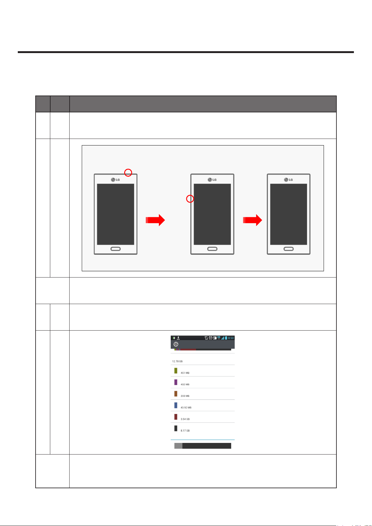
1) Default available memory capacity on the phone is marked in the image attached.
2) Actual memory size available to customers need be marked.
Total space
App
Photo, video
Audio(Music, Ringtones,podcast, etc.)
Download
Others
Available
SD Card
- 29 -
Copyright © 2013 LG Electronics. Inc. All right reserved.
Only for training and service purposes
Page 30
4. TROUBLE SHOOTING
4.1 RF Component
X2000
VCTCXO
FL1004
W2100 Tx SAW
RF Transceiver
FL1003
W2100 Rx SAW
U1000
FL1001
EGSM/850 Rx SAW
FL1002
DCS/PCS Rx SAW
FL1006
W2100
DPX
U1002
FL1007
W2100
W900 DPX
PAM
4. TROUBLE SHOOTING
U1001
GSM PAM
+ASM
U1003
W900
PAM
SW100
Mobile Switch
LGE Internal Use Only
- 30 -
Copyright © 2013 LG Electronics. Inc. All right reserved.
Only for training and service purposes
Page 31

4. TROUBLE SHOOTING
RF component (WCDMA / GSM)
Reference Description Reference Description
U1000 RTR6285A(Transceiver) FL1007 WCDMA (VIII) Duplexer
U1001 GSM TX Module (ASM+GSM PAM) FL1003 WCDMA (I) RX SAW Filter
U1002 WCDMA (I) PAM FL1001 EGSM/850 Rx saw lter
U1003 WCDMA (VIII) PAM FL1002 DCS/PCS Rx saw lter
FL1004 WCDMA (I) TX SAW Filter X2000 VCTCXO(19.2MHz)
FL1006 WCDMA (I) Duplexer SW1000 RF Antenna Connector
LGE Internal Use Only
- 31 -
Copyright © 2013 LG Electronics. Inc. All right reserved.
Only for training and service purposes
Page 32

4.2 SIGNAL PATH
4. TROUBLE SHOOTING
LGE Internal Use Only
WCDMA I and VIII Band TX Signal PATH
D2. WCDMA 2100 TX PATH
E2. WCDMA 900 TX PATH
F1. COMMON TX/RX PATH
- 32 -
Copyright © 2013 LG Electronics. Inc. All right reserved.
Only for training and service purposes
Page 33

4. TROUBLE SHOOTING
WCDMA I and
VIII
Band RX Signal PATH
D1. WCDMA 2100 RX PATH
E1. WCDMA 900 RX PATH
F1. COMMON TX/RX PATH
LGE Internal Use Only
- 33 -
Copyright © 2013 LG Electronics. Inc. All right reserved.
Only for training and service purposes
Page 34

4. TROUBLE SHOOTING
LGE Internal Use Only
GSM850/GSM900/DCS/PCS’s RX/TX Signal PATH
A. GSM850/GSM900/DCS1800/PCS1900 RX PATH
B. GSM850/GSM900/DCS1800/PCS1900 TX PATH
C1. COMMON TX/RX PATH
- 34 -
Copyright © 2013 LG Electronics. Inc. All right reserved.
Only for training and service purposes
Page 35

4. TROUBLE SHOOTING
4.3 Checking TCXO Block
The output frequency (19.2MHz) of TCXO (X2000) is used as the reference one of RTR6285 and PM8029 internal VCO.
TP1
TP2
TP3
VREG_TCXO_2.85V
TP1
TRK_LO_ADJ
C2006
C2005
0.1u
Clesed to TCXO
R2003 100
TP2
TCXO Circuit
1n
X2000
1XXA19200FBB
4
VCC
1
VCONT
19.2MHz
C2009
10n
Rev.D update
Schematic of the Crystal Part (19.2MHz)
OUT
GND
3
2
1nC2017
TP3
TCXO_PM_19.2MHZ
TCXO_RTR_19.2MHZ
LGE Internal Use Only
- 35 -
Copyright © 2013 LG Electronics. Inc. All right reserved.
Only for training and service purposes
Page 36

Check TP1
VCC of TCXO
4. TROUBLE SHOOTING
VCC ≥ 2.8V
Yes
Check TP2
2.4V ≥ Voltage ≥ 0.4V
Yes
Check TP3
19.2 MHz Signal
Yes
No
No
No
Check PM8029
Check MSM7225A
Check soldering and
components
LGE Internal Use Only
TCXO is OK
- 36 -
Copyright © 2013 LG Electronics. Inc. All right reserved.
Only for training and service purposes
Page 37

4. TROUBLE SHOOTING
4.4 Checking GSM TX Module(GSM PAM + ASM) Block
VBATT(TP1)
ANT_SEL1
ANT_SEL2
ANT_SEL0
TX_EN
LGE Internal Use Only
- 37 -
Copyright © 2013 LG Electronics. Inc. All right reserved.
Only for training and service purposes
Page 38

4. TROUBLE SHOOTING
FL1001
6
7
8
9
FL1002
6
7
8
9
DCS_PCS_TX
DCS(1710-1785 MHz)
PCS(1850-1910 MHz)
GSM850_GSM900_TX
GSM850(824-849MHz)
GSM900(880-915MHz)
R1012
R1007
W850_W900_RTX
RX_PCS_P
W1900_W2100_RTX
24
23
25
28
261927
44
TRX4
GND11
PGND7
PGND9
PGND8
373635
2mm
C1118
6.8p
C1125
DNI
PGND16
PGND15
PGND14
PGND13
GND10
TRX3
TRX2
TRX1
VRAMP
TXEN
MODE
GND9
PGND12
PGND11
PGND10
VBAT
C1039
100p
C1124
DNI
C1038
10u
43
42
41
22
21
20
18
17
16
15
40
39
38
ANT_SEL1
ANT_SEL2
ANT
GND13
GND14
U1001
TX_LB_IN
BS2
BS1
GND12
VBATT
VCC
1413121110
1
GND1
2
GND2
3
GND3
4
GND4
5
GND5
6
GND6
7
GND7
8
GND8
29
PGND1
30
PGND2
31
PGND3
32
PGND4
33
PGND5
34
PGND6
TX_HB_IN
9
R1011
47
7dB
R1006
11dB
130
R1013
75
91
R1008
130
91
C10221.2n
TP1
C1046
100p
L1004
4.7n
L1009
8.2n
1
GSM1800/1900_IN
2
GND1
3
GND2
4
GND3
1
GSM850/900_IN
2
GND1
3
GND2
4
GND3
C1047
39p
C1126
DNI
R1002
2.2K
RX_PCS_M
C1123
DNI
GND5GND4
GSM1900_Bal_OUT2
GSM1900_Bal_OUT1
GSM1800_Bal_OUT2
GSM1800_Bal_OUT1
5 10
GND5GND4
GSM900_Bal_OUT2
GSM900_Bal_OUT1
GSM850_Bal_OUT2
GSM850_Bal_OUT1
5 10
GSM_PA_RAMP
GSM_PA_EN
ANT_SEL0
Schematic of the Antenna Switch Block
Antenna Switch Module logic(SKY77584)
ANT_SEL 0 ANT_SEL 1 ANT_SEL 2 Tx_EN
STAND-BY LOW LOW LOW LOW
GTX_LB LOW LOW HIGH HIGH
GTX_HB LOW HIGH HIGH HIGH
GRX_LB HIGH LOW LOW LOW
GRX_HB HIGH HIGH LOW LOW
WTRX_HB HIGH LOW HIGH LOW
WTRX_LB LOW HIGH LOW LOW
LGE Internal Use Only
- 38 -
Copyright © 2013 LG Electronics. Inc. All right reserved.
Only for training and service purposes
Page 39

Checking Switch Block Power Source
Check ANT_SEL 0,1,2,3
High Level
4. TROUBLE SHOOTING
1.2V < Voltage < 3V
Yes
Check the Logic
In each mode
No
Check the TP1(VBATT)
LGE Internal Use Only
- 39 -
Copyright © 2013 LG Electronics. Inc. All right reserved.
Only for training and service purposes
Page 40

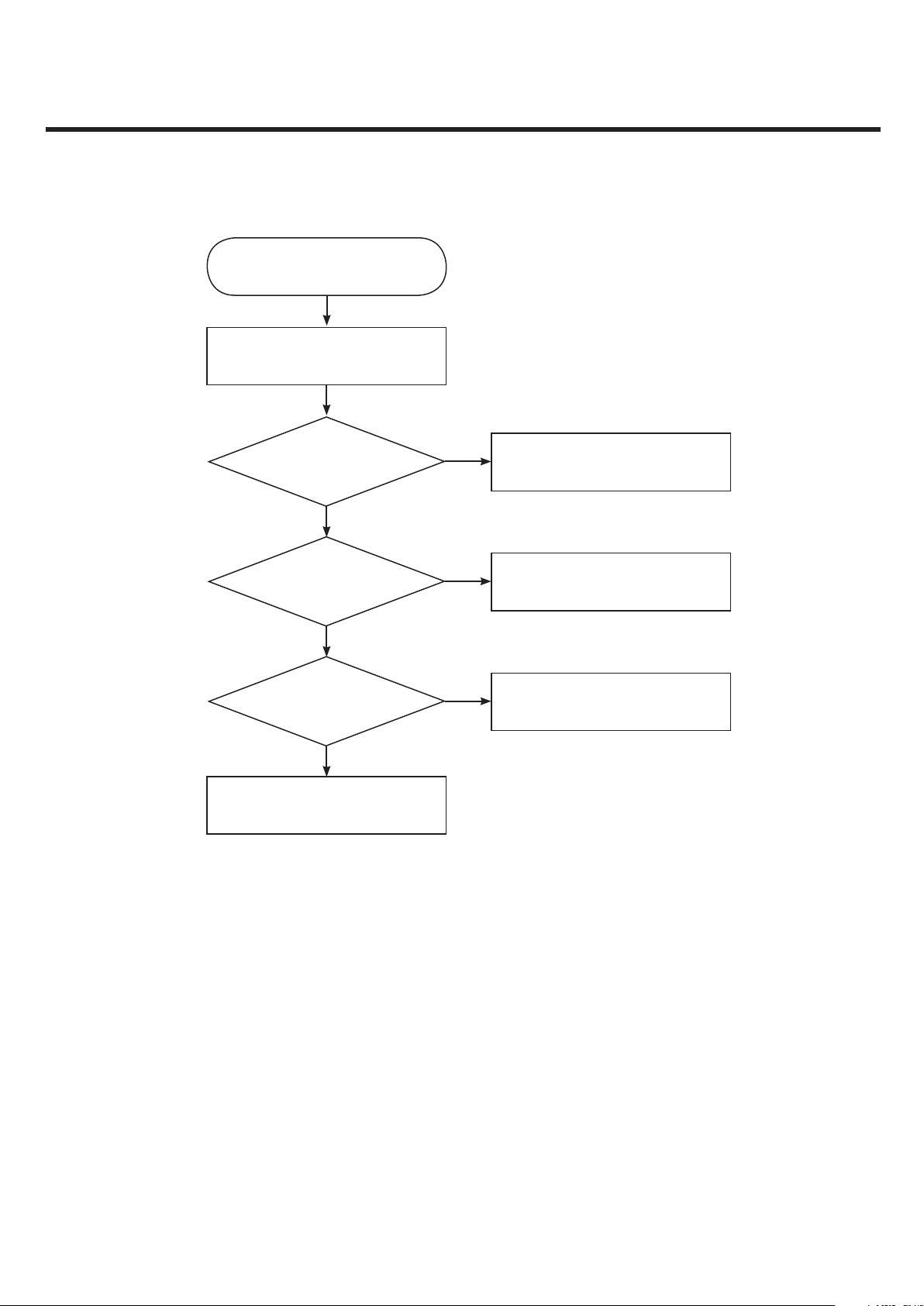
4.5 Checking WCDMA Block
4. TROUBLE SHOOTING
START
1. Check TCXO 19.2MHz
2. Check Tx Module Block
Refer to 1.4
3. Check RF Tx Level
4. Check PAM Block
Refer to 1.5.4
5. Check RF Level
6. Ro-download SW & Cal.
LGE Internal Use Only
- 40 -
Copyright © 2013 LG Electronics. Inc. All right reserved.
Only for training and service purposes
Page 41

4.5.1Checking TCXO Block
Refer to 4.3
4.5.2. Checking Tx Module Block
Refer to 4.4
4.5.3. Checking RF TX Level
4. TROUBLE SHOOTING
TP3
Test Point (TX Level)
TP4
TP2
TP1
LGE Internal Use Only
- 41 -
Copyright © 2013 LG Electronics. Inc. All right reserved.
Only for training and service purposes
Page 42

C1128
100p
4. TROUBLE SHOOTING
C1010
0.75p
MBV62422401
FEED
ANT1002
MBV62422401
FEED
ANT1001
100p
C1127
REV_1.1
C1002 6.8p
2
C1005
100n
L1001
15n
W850_W900_RTX
W1900_W2100_RTX
C1022 1.2n
C1046
100p
L1004
4.7n
L1009
8.2n
1
2
3
4
1
2
3
4
L1037
8.2n
SW1000
COMMON
ANT
1
G3 G4
43
DNI
C1007
C1003
DNI
100pC1001
TP1
24
23
2520261927
28
44
TRX4
PGND7
PGND8
37
36
PGND9
PGND16
PGND15
PGND14
PGND13
GND10
TRX3
TRX2
TRX1
VRAMP
TXEN
MODE
GND9
PGND12
PGND11
PGND10
43
42
41
22
21
18
17
16
15
40
39
38
29
30
31
32
33
34
1
2
3
4
5
6
7
8
GND1
GND2
GND3
GND4
GND5
GND6
GND7
GND8
PGND1
PGND2
PGND3
PGND4
PGND5
PGND6
TX_HB_IN
TX_LB_IN
9
10
ANT
GND13
GND14
U1001
BS2
BS1
VBATT
VCC
14
131211
GND12
GND11
35
W1900_W2100_RTX
TP2
W850_W900_RTX
LGE Internal Use Only
C1112
DNI
L1015 2n
C1076
DNI
L1020
DNI
FL1006
ANT
GND1 GND6
GND2 GND5
GND3 GND4
1950MHz,2140MHz
Band I
16
RX
3
TX
92
84
75
L1022 10p
C1089
DNI
PDET_IN
C1091
0.75p
8.2pC1085
L1021
3.9n
RX_WCDMA_HB
L1016
3.6n
VBAT
C1081
C1082
2.2u
330p
11
PGND
10 1
RF_OUT RF_IN
8 3
VMODE1CPL_IN
7
GND
VMODE0
6
CPL_OUT
REV_1.1
R1017
51
R1018
R1019
8dB
110
110
C1080
U1002
VBATVCC
VEN
Close to pin1
330p
29
4
5
3G_PAM_MODE
PA_R0
PA_ON0
C1093
C1094
DNI
DNI
L1023 4.7n
C1090
0.5p
FL1004
4 1
OUT
5 3 2
1950MHz
IN
G1G2G3
3.3nC1087
W1900_W2100_TX_OUT
C1088
DNI
TP4
TP3
VBAT
3.3pL1029
RX_WCDMA_900_P
L10313.3p
L1034 3.9p
C1116
8.2n
C1103
6.8n
C1117
27n
RX_WCDMA_900_M
C1104
FL1007
33pC1111
L1033
5.6n
RX1
ANT
RX2
2
GND1
4 9
GND5GND2
GND3 GND4
16
8
3
TX
75
DNI
C1097
C1096
680p
2.2u
11
PGND
10 1
RF_OUT RF_IN
8 3
VMODE1CPL_IN
7
GND
VMODE0
6
CPL_OUT
49.9
R1022
REV_1.1
Band VIII
- 42 -
C1095
680p
U1003
VBATVCC
29
4
5
VEN
3G_PAM_MODE
PA_R0
PA_ON1
C1109
C1110
DNI
DNI
FL1008
897.5MHz
L1102
5 3 2
12n
IN
G1G2G3
C1108
DNI
4.7nC1101
4 1
OUT
C1107
DNI
Copyright © 2013 LG Electronics. Inc. All right reserved.
Only for training and service purposes
W850_W900_TX_OUT
Page 43

Check ANT_SEL 0,1,2
(High, Low, Low)
4. TROUBLE SHOOTING
Check TP1 Over 21dBm?
No
Check TP2 Over 21dBm?
No
Check TP3 Over 21dBm?
No
Check TP4 Over 7dBm?
No
Check PAM Block
Refer to 1.5.4
Yes
RF Tx Level is OK
Yes
Check TX Module
Yes
Check Duplexer
Yes
Check RTR6285A
RTR6285 Maximum output Power = 7 dBm
RTR6285 minimum output Power = -80 dBm
LGE Internal Use Only
- 43 -
Copyright © 2013 LG Electronics. Inc. All right reserved.
Only for training and service purposes
Page 44

4.5.4. Checking PAM Block
PAM Control Signal
PA_ON0 (C1094), PA_ON1(C1110) : PAM Enable
PA_R0: PAM Gain Control
PA_ON must be HIGH (over 2.6V)
PAM IN/OUT Signal :
When PAM is under the operation of high power mode (PA_R0(C1093) : Low),
PAM OUT power must be over 21 dBm
PAM IN power must be under 10 dBm
4. TROUBLE SHOOTING
TP2
TP1
TP3
LGE Internal Use Only
- 44 -
Copyright © 2013 LG Electronics. Inc. All right reserved.
Only for training and service purposes
Page 45

4. TROUBLE SHOOTING
W1900_W2100_RTX
W850_W900_RTX
L1020
DNI
FL1006
ANT
GND1 GND6
GND2 GND5
GND3 GND4
1950MHz,2140MHz
Band I
16
RX
3
TX
92
84
75
8.2pC1085
L1021
3.9n
TP3
FL1007
33pC1111
C1112
L1033
DNI
5.6n
Set the phone Tx is On and
16
RX1
ANT
8
RX2
3
TX
2
GND1
4 9
GND5GND2
75
GND3 GND4
Band VIII
PDM is 210
C1076
DNI
L1022 10p
C1089
DNI
L1015 2n
PDET_IN
C1091
0.75p
RX_WCDMA_HB
L1016
3.6n
VBAT
C1081
C1082
2.2u
330p
U1002
11
PGND
10 1
VBATVCC
RF_OUT RF_IN
8 3
VMODE1CPL_IN
7
GND
VMODE0
6
CPL_OUT
REV_1.1
R1017
51
R1018
R1019
8dB
110
110
C1080
Close to pin1
330p
29
4
5
VEN
3G_PAM_MODE
PA_R0
PA_ON0
C1093
C1094
DNI
DNI
L1023 4.7n
C1090
0.5p
FL1004
4 1
OUT
5 3 2
1950MHz
IN
G1G2G3
3.3nC1087
W1900_W2100_TX_OUT
C1088
DNI
TP1
VBAT
3.3pL1029
RX_WCDMA_900_P
L10313.3p
L1034 3.9p
C1116
8.2n
C1103
6.8n
C1117
27n
RX_WCDMA_900_M
C1104
DNI
C1097
C1096
680p
2.2u
TP2
11
PGND
10 1
RF_OUT RF_IN
8 3
7
GND
6
CPL_OUT
49.9
R1022
REV_1.1
VMODE1CPL_IN
VMODE0
C1095
680p
U1003
VBATVCC
29
4
5
VEN
3G_PAM_MODE
PA_R0
PA_ON1
C1109
C1110
DNI
DNI
FL1008
897.5MHz
L1102
5 3 2
12n
IN
G1G2G3
W850_W900_TX_OUT
C1108
DNI
4.7nC1101
4 1
OUT
C1107
DNI
Check TP3 Over 21dBm?
No
Check TP2 PA_R0 ≥ 2.6V
No
Check TP1 Over 10 dBm?
No
Change the board
Yes
RF Tx Level is OK
Yes
Check MSM7225A
Yes
Check RTR6285A
LGE Internal Use Only
- 45 -
Copyright © 2013 LG Electronics. Inc. All right reserved.
Only for training and service purposes
Page 46

4.5.5. Checking RF Rx Level
4. TROUBLE SHOOTING
Test Point (RF Rx Level)
TP5
TP2
Bias
TP1
TP3
LGE Internal Use Only
- 46 -
Copyright © 2013 LG Electronics. Inc. All right reserved.
Only for training and service purposes
Page 47

C1128
100p
4. TROUBLE SHOOTING
C1010
0.75p
MBV62422401
FEED
ANT1002
MBV62422401
FEED
ANT1001
100p
C1127
REV_1.1
C1002 6.8p
2
C1005
100n
L1001
15n
W850_W900_RTX
W1900_W2100_RTX
C1022 1.2n
C1046
100p
L1004
4.7n
L1009
8.2n
1
2
3
4
1
2
3
4
L1037
8.2n
SW1000
ANT
G3 G4
COMMON
43
1
DNI
C1007
C1003
DNI
100pC1001
TP1
24
23
2520261927
28
44
TRX4
PGND7
PGND8
37
36
PGND9
PGND16
PGND15
PGND14
PGND13
GND10
TRX3
TRX2
TRX1
VRAMP
TXEN
MODE
GND9
PGND12
PGND11
PGND10
43
42
41
22
21
18
17
16
15
40
39
38
29
30
31
32
33
34
1
2
3
4
5
6
7
8
GND1
GND2
GND3
GND4
GND5
GND6
GND7
GND8
PGND1
PGND2
PGND3
PGND4
PGND5
PGND6
TX_HB_IN
TX_LB_IN
9
10
ANT
GND13
GND14
U1001
BS2
BS1
VBATT
VCC
14
131211
GND12
GND11
35
LGE Internal Use Only
- 47 -
Copyright © 2013 LG Electronics. Inc. All right reserved.
Only for training and service purposes
Page 48

4. TROUBLE SHOOTING
W1900_W2100_RTX
W850_W900_RTX
TP2
C1112
DNI
L1015 2n
C1076
DNI
L1020
DNI
FL1006
ANT
GND1 GND6
GND2 GND5
GND3 GND4
1950MHz,2140MHz
Band I
16
RX
3
TX
92
84
75
L1022 10p
C1089
DNI
PDET_IN
C1091
0.75p
8.2pC1085
L1021
3.9n
RX_WCDMA_HB
L1016
3.6n
VBAT
C1081
C1082
2.2u
330p
U1002
11
PGND
10 1
VBATVCC
RF_OUT RF_IN
8 3
VMODE1CPL_IN
7
GND
VMODE0
6
CPL_OUT
REV_1.1
R1017
51
R1018
R1019
8dB
110
110
C1080
Close to pin1
330p
29
4
5
VEN
3G_PAM_MODE
PA_R0
PA_ON0
C1093
C1094
DNI
DNI
L1023 4.7n
C1090
0.5p
FL1004
4 1
OUT
5 3 2
1950MHz
IN
G1G2G3
3.3nC1087
W1900_W2100_TX_OUT
C1088
DNI
TP3
VBAT
3.3pL1029
RX_WCDMA_900_P
L10313.3p
L1034 3.9p
C1116
8.2n
C1103
6.8n
C1117
27n
RX_WCDMA_900_M
C1104
FL1007
33pC1111
L1033
5.6n
RX1
ANT
RX2
2
GND1
4 9
GND5GND2
GND3 GND4
16
8
3
TX
75
DNI
C1097
C1096
680p
2.2u
11
PGND
10 1
RF_OUT RF_IN
8 3
VMODE1CPL_IN
7
GND
VMODE0
6
CPL_OUT
49.9
R1022
REV_1.1
Band VIII
C1095
680p
U1003
VBATVCC
29
4
5
VEN
3G_PAM_MODE
PA_R0
PA_ON1
C1109
C1110
DNI
DNI
FL1008
897.5MHz
L1102
5 3 2
12n
IN
G1G2G3
W850_W900_TX_OUT
C1108
DNI
4.7nC1101
4 1
OUT
C1107
DNI
Bias
VDD_RX
RX_WCDMA_2100_LNA_OUT
RX_WCDMA_1900_LNA_OUT
C1077 0.1u
R1015
R1016
DNI
0
100pC1078
WCDMA RX 2100 LNA Circuit
1KR1014
L1017
2n
FL1003
4.7n
IN
G1 G3
OUT
_OUT
52
2140MHz
31
4
L1019
33p
C1086
C1084
8.2n
C1079
C1092
DNI
C1083
L1018
1.8n
WB2100_MIX_INP
W2100 RX(2110 - 2170 MHz)
L1024
1.8n
WB2100_MIX_INM
2.7p
2.7p
TP5
LGE Internal Use Only
- 48 -
Copyright © 2013 LG Electronics. Inc. All right reserved.
Only for training and service purposes
Page 49

Set the phone Rx is On
4. TROUBLE SHOOTING
Check BIAS over 2.1 V?
Yes
Check TP1 Signal exist?
Yes
Check TP2 Signal exist?
Yes
Check TP3 Signal exist?
Yes
Check TP4 Signal exist?
No
Check bias block soldering
No
Check RF Switch (M/S)
No
Check TX Module Refer 1.4
No
Check Duplexer
No
DNI SKIP
LGE Internal Use Only
Yes
Check TP5 Signal exist?
Yes
Change the board
No
- 49 -
Check RTR6285 and Rx SAW lter
Copyright © 2013 LG Electronics. Inc. All right reserved.
Only for training and service purposes
Page 50

4.6 Checking GSM Block
4. TROUBLE SHOOTING
START
1. Check TCXO Block
2. Check Tx Module
3. Check RF TRX Level
4. Ro-download SW & Cal.
LGE Internal Use Only
- 50 -
Copyright © 2013 LG Electronics. Inc. All right reserved.
Only for training and service purposes
Page 51

4. TROUBLE SHOOTING
1
2,3
LGE Internal Use Only
- 51 -
Copyright © 2013 LG Electronics. Inc. All right reserved.
Only for training and service purposes
Page 52

4.6.1 Checking TCXO Block
Refer to 4.3
4.6.2 Checking Tx module Block
Refer to 4.4
4.6.3 Checking RF TX level
4. TROUBLE SHOOTING
TP3
TP2
TP1
LGE Internal Use Only
- 52 -
Copyright © 2013 LG Electronics. Inc. All right reserved.
Only for training and service purposes
Page 53

100p
C1046
C1010
DNI
8.2n
L1009
DNI
L1004
4.7n
C1022 1.2n
W850_W900_RTX
W1900_W2100_RTX
0.75p
MBV62422401
FEED
ANT1002
TP2
MBV62422401
FEED
ANT1001
100p
C1127
C1128
100p
C1007
DNI
29
30
31
32
33
34
1
2
3
4
5
6
7
8
C1003
DNI
GND1
GND2
GND3
GND4
GND5
GND6
GND7
GND8
PGND1
PGND2
PGND3
PGND4
PGND5
PGND6
TX_HB_IN
TX_LB_IN
9
11
10
100pC1001
2520261927
28
ANT
GND13
GND14
U1001
BS2
BS1
VBATT
VCC
14
13
12
REV_1.1
SW1000
ANT
1
23
TRX4
PGND7
36
35
PGND8
PGND9
37
G3 G4
PGND16
PGND15
PGND14
PGND13
GND10
VRAMP
PGND12
PGND11
PGND10
L1037
8.2n
24
GND12
GND11
4. TROUBLE SHOOTING
TP1
C1002 6.8p
C1005
100n
L1001
15n
COMMON
43
TRX3
TRX2
TRX1
TXEN
MODE
GND9
2
44
43
42
41
22
21
18
17
16
15
40
39
38
DCS_PCS_TX
DCS(1710-1785 MHz)
PCS(1850-1910 MHz)
GSM850_GSM900_TX
GSM850(824-849MHz)
GSM900(880-915MHz)
LGE Internal Use Only
TP3
R1012
R1007
2mm
C1118
6.8p
C1039
100p
VBAT
C1038
10u
R1011
47
7dB
130
R1006
75
91
11dB
R1013
R1008
130
91
ANT_SEL1
ANT_SEL2
C1124
C1125
Schematic of GSM/DCS/PCS Tx Block
- 53 -
Copyright © 2013 LG Electronics. Inc. All right reserved.
Only for training and service purposes
Page 54
START
Check TCXO Block Refer to 1.3
4. TROUBLE SHOOTING
Check TP1
If GSM over 31 dBm?
If DCS/PCS over 28 dBm?
No
Check TP2, 3
If GSM(TP2) under 6 dBm?
If DCS/PCS(TP3) under 6 dBm?
No
Check RTR & PAD
Still exist Problem
Change the board
Yes
Yes
No Problem
GSM/DCS/PCS Tx is OK
Check other part
Check Tx Module
(ASM+EDGE PAM)
Refer to 4.4
Check soldering and components
LGE Internal Use Only
- 54 -
Copyright © 2013 LG Electronics. Inc. All right reserved.
Only for training and service purposes
Page 55

4.6.4 Checking RF Rx Block
4. TROUBLE SHOOTING
TP2
C1010
0.75p
MBV62422401
FEED
ANT1002
MBV62422401
FEED
ANT1001
100p
C1127
C1128
C1007
TP1
100p
REV_1.1
DNI
C1003
100pC1001
DNI
SW1000
COMMON
ANT
1
G3 G4
L1037
43
8.2n
C1002 6.8p
2
L1001
C1005
15n
100n
TP1
TP2
1
GSM1800/1900_IN
2
GND1
3
GND2
4
GND3
1
GSM850/900_IN
2
GND1
3
GND2
4
GND3
RX_PCS_P
RX_PCS_M
GND5GND4
GSM1900_Bal_OUT2
GSM1900_Bal_OUT1
GSM1800_Bal_OUT2
GSM1800_Bal_OUT1
5 10
GND5GND4
GSM900_Bal_OUT2
GSM900_Bal_OUT1
GSM850_Bal_OUT2
GSM850_Bal_OUT1
5 10
9
8
7
6
FL1002
9
8
7
6
FL1001
W850_W900_RTX
W1900_W2100_RTX
24
23
2520261927
28
ANT
TRX4
GND13
GND12
GND11
9
TX_HB_IN
TX_LB_IN
GND14
U1001
BS2
BS1
VBATT
1413121110
PGND7
PGND8
VCC
1
GND1
2
GND2
3
GND3
4
GND4
5
GND5
6
GND6
7
GND7
8
GND8
29
PGND1
30
PGND2
31
PGND3
32
PGND4
33
PGND5
34
PGND6
373635
PGND9
PGND16
PGND15
PGND14
PGND13
GND10
TRX3
TRX2
TRX1
VRAMP
TXEN
MODE
GND9
PGND12
PGND11
PGND10
44
43
42
41
22
21
18
17
16
15
40
39
38
C10221.2n
C1046
L1004
4.7n
100p
L1009
8.2n
C1013 1.5n
DNI
L1003
C1024 1.5n
L1006
DNI
L1007
DNI
L1012
10n
C1028 8.2p
C1048 10p
L1035 8.2n
L1036 8.2n
8.2pC1040
10pC1041
L1002
2.2n
PCS(1930-1990 MHz)
RX_DCS_P
L1005
DCS(1805-1880 MHz)
3.9n
RX_DCS_M
RX_GSM_900_P
L1008
GSM(925-960 MHz)
15n
RX_GSM_850_P
GSM(869-894 MHz)
L1013
DNI
RX_GSM_850_M
GPS_IN
RX_GSM_900_M
LGE Internal Use Only
Schematic of GSM/DCS/PCS Rx Block
- 55 -
Copyright © 2013 LG Electronics. Inc. All right reserved.
Only for training and service purposes
Page 56

Set the phone Rx is On
4. TROUBLE SHOOTING
Check TP1 Signal exist ?
Yes
Check TP2 Signal exist ?
Yes
Change the board
No
No
Check RF Switch (M/S)
Check Tx Module
Refer to 4.4
LGE Internal Use Only
- 56 -
Copyright © 2013 LG Electronics. Inc. All right reserved.
Only for training and service purposes
Page 57

4.7 GPS/WIFI/BT RF Component
FL1005
ANT1004
4. TROUBLE SHOOTING
U1004
GPS Component
Reference Description
ANT1004 C-CLIP
connected to Carrier type antenna
FL1005 GPS SAW FILTER
U1004 GPS LNA
LGE Internal Use Only
- 57 -
Copyright © 2013 LG Electronics. Inc. All right reserved.
Only for training and service purposes
Page 58

FL9000
U9001
4. TROUBLE SHOOTING
ANT9001
U9000
BT/WiFi Component
Reference Description
ANT9001 ANTENNA PAD
connected to Carrier type antenna
U9000 BT module
U9001 WiFi module
FL9000 FEM
LGE Internal Use Only
- 58 -
Copyright © 2013 LG Electronics. Inc. All right reserved.
Only for training and service purposes
Page 59

4.8 GPS/WIFI/BT SIGNAL PATH
4. TROUBLE SHOOTING
GPS Signal PATH (main board bottom)
GPS Rx PATH
WLAN_Tx
BT TRx
WLAN_Rx
LGE Internal Use Only
WiFi / BT Signal PATH
WiFi / BT Txand Rx PATH
- 59 -
Copyright © 2013 LG Electronics. Inc. All right reserved.
Only for training and service purposes
Page 60

4.9 GPS/WIFI/BT Trouble shooting
4.9.1 A-GPS Block
4. TROUBLE SHOOTING
L1028
100p
MBV62422401
FEED
ANT1004
L1026
5.6n
C1098
100p
L1027
TP1
1575.42 MHz
DNI
GPS_MODE
FL1005
3
G3
IN OUT
G1 G2
52
TP2
41
C1115
6.8p
R1023
C1099
DNI
12
L1025
LNA for the GPS
3.3n
TP1
C1100
DNI
1
VDD
GND
RF_IN
3
S_D
2
FIL_OUT
U1004
5
4
L1030
4.7n
C1113
DNI
Near To LNA
C1105
18p
L1032
3.3n
R1021
12
C1114
DNI
C1106
0.1u
VREG_RF_2.7V_RTR
GPS_IN
LGE Internal Use Only
TP2
- 60 -
Copyright © 2013 LG Electronics. Inc. All right reserved.
Only for training and service purposes
Page 61

Set the phone GPS is ON
4. TROUBLE SHOOTING
Check TP1 About 2.7V?
Yes
Check TP2 About 2.6V?
Yes
Change the board
No
Check power LRC lter soldering
No
Check SW and NV item
LGE Internal Use Only
- 61 -
Copyright © 2013 LG Electronics. Inc. All right reserved.
Only for training and service purposes
Page 62

4.9.2 WLAN/BT/FM Block
4. TROUBLE SHOOTING
1
3
START
1. Check the Power
2. Check the Clock
3
2
LGE Internal Use Only
3. Check the Module
Component Change
- 62 -
Copyright © 2013 LG Electronics. Inc. All right reserved.
Only for training and service purposes
Page 63

4. TROUBLE SHOOTING
BT/WI-FI FRONT-END
Module part
ANT9001
C9003
100p
L9007
100n
C9000 100p
L9000
0.5p
L9001
DNI
BT_WLAN_RF
FL9000
WLAN_TX
BT_TRX
GND1
GND2
GND3
GND4
PGND
1
5
6
8
9
10
13
WLAN_SW_[0]
WLAN_SW_[1]
WLAN_SW_[2]
BT_WLAN_RF
WLAN_PWR_DET_IN
C9009
DNI
C9010
DNI
C9011
DNI
3
WLAN_RX
4
TR_SW0
2
TR_SW1
12
TR_SW2
7
ANT
11
CPL
2400MHz,2500MHz
C9005
DNI
L9002
3.9n
L9005
2.4n
C9006
DNI
C9012 22p
C9013
DNI
C9007
DNI
C9014
DNI
C9004
DNI
WLAN_RF_RX
WLAN_RF_TX
BT_RF_QCT
LGE Internal Use Only
ANTENNA SWITCH MODULE LOGIC
SW2SW1SW0
WiFi RX-ANT LOW
WiFi TX-ANT
BT-ANT
- 63 -
HIGH
LOW
LOW HIGH
HIGH
LOW
Copyright © 2013 LG Electronics. Inc. All right reserved.
Only for training and service purposes
LOW
LOW
Page 64

FM_ANT
WiFi : WCN 1314
4. TROUBLE SHOOTING
FM_L
BT_FM_CLK_WCN
BT_FM_CLK_REQ_WCN
BT_PRIORITY
FM_R
BT_PCM_SYNC
BT_PCM_IN
FM_RDS_INT
BT_ACTIVE
WLAN_ACTIVE
BT_RF_QCT
BT/FM Module : WCN2243
1MR9000
C9002
22p
VREG_MSME_1.8V
BT_RST_N
I2C_COMMON_SDA_WCN
C9008
47p
I2C_COMMON_SCL_WCN
L9004
L9006
82n
82n
BT_PCM_OUT
BT_PCM_IN
BT_PCM_SYNC
BT_PCM_CLK
BT_PCM_OUT
BT_PCM_CLK
SLEEP_CLK
BT_UART_TX
BT_UART_RX
BT_UART_RTS
BT_UART_CTS
L9003
68n
R9001
R9002
2.2K
2.2K
6
GND1
33
SYS_RST_N
28
I2C_SDA
29
I2C_SCL
43
FM_HRX_IN
49
DNIR9003
FM_PRXTX_IO
46
FM_I2S_SD
56
FM_I2S_WS
51
FM_I2S_SCK
58
BT_PCM_IN
42
BT_PCM_CLK
53
SLEEP_CLK
36
BT_UART_RXD
47
BT_UART_TXD
40
BT_UART_CTS
57
BT_UART_RTS
R9004
1M
GND2
41
SYS_CLK
FM_RDS_INT
GND3
AGND_FM1
FM_LO_L
FM_LO_R
AGND_FM2
AGND_FM3
U9000
AGND_FM4
BT_CLK_REQ
BT_PCM_OUT
BT_PCM_SYNC
AGND_FM
GND4
22164439384823
BT_ACTIVE
AGND_BT1
8
BT_STATUS
TX_CONFIRM
AGND_BT2
AGND_BT3
2189
334353017205226272545
BT_RFIO
AGND_BT4
AGND_BT5
VDD_IO
VDD_XO_BIAS
VREG_DIG
VREG_ANA
VDD_LDO_IN
VDD_FM_1P3_1
VDD_FM_1P3_2
VDD_FM_1P3_3
VDD_FM_1P3_4
VDD_DIG_1P3
VDD_FM_DAC
VDD_BT_PA
VDD_BT_1P3_1
VDD_BT_1P3_2
VDD_BT_1P3_3
VDD_BT_1P3_4
AGND_BT6
AGND_BT7
1117
31
24
14
4
10
54
37
50
55
21
32
19
13
12
15
5
C9018
C9017
C9015
C9016
10n
C9019
4.7u
10p
10n
10n
C9023
C9022
C9020
C9021
4.7u
C9024
10n
10n
0.1u
VREG_MSME_1.8V
+3V_WLAN_WCN
C9025
1u
10p
+1V2_WLAN_WCN
+1V2_MSM_A2_WCN
VREG_MSME_1.8V
+1V8_WLAN_TCXO
+1V3_MSM_A3_WCN
+3V_WLAN_WCN
R9007
close to pin5
close to pin13
close to pin54
close to pin37
79
U9001
GND_A21
GND_D1
GND_D2
GND_D3
GND_D4
GND_A1
GND_A22
GND_D5
GND_D6
GND_D7
GND_D8
GND_A2
GND_A23
GND_A3
GND_A4
GND_D9
GND_A5
GND_A6
GND_A7
GND_A8
GND_A9
GND_A10
GND_A11
GND_A12
GND_A13
GND_A14
GND_A15
GND_A16
GND_A17
GND_A18
GND_A19
GND_A20
3
7
1
10
30
58
24
32
37
47
70
64
86
52
34
60
72
73
61
44
65
83
50
59
68
69
57
55
42
40
43
C9027
C9028
4.7u
0.1u
31
C9043
100p
46
48
5
36
38
8
2
4
85
77
78
51
35
74
66
81
67
54
76
62
49
VDD_CORE1
VDD_CORE2
VDD_CORE3
VDD_CORE_AON1
VDD_CORE_AON2
VDD_CORE_AON3
VDD_IO
VDD_FEM
VDD_SDIO
VDD_RFA10
VDD_RFA11
VDD_PA
VDD_TCXO
VDD_RFA1
VDD_RFA2
VDD_RFA3
VDD_RFA4
VDD_RFA5
VDD_RFA6
VDD_RFA7
VDD_RFA8
VDD_RFA9
C9026
10n
C9029
0.1u
C9032
C9037
22u
C9031
0.1u
100p
colse to pin85
C9038
C9040
C9039
10n
100p
100p
FB9001
60
C9042
0.1u
C9034
220n
colse to pin77
FB9000
C9036
240
470n
0
C9033
2.2u
C9041
2.2u
colse to pin78
LGE Internal Use Only
[Figure] Schematic of WiFi/BT module
- 64 -
Copyright © 2013 LG Electronics. Inc. All right reserved.
Only for training and service purposes
Page 65

4. TROUBLE SHOOTING
TP2
TP1
Test point Description
Test point Net name Description
TP1 +3V_WLAN_WCN Power for BT/WiFi BB core and WiFi power Amp. (V Batt)
TP2 VREG_MSME_1.8V Power for BT power Amp. (1.8V)
TP3 VREG_MSME_1.8V Power for host interface (1.8V)
START
TP3
LGE Internal Use Only
TP1, 2, 3 is OK?
Yes
SDIO ok?
UART ok?
No
Board Change
- 65 -
No
Check the power block
Yes
Module Check
Copyright © 2013 LG Electronics. Inc. All right reserved.
Only for training and service purposes
Page 66

4. TROUBLE SHOOTING
4.10 Power ON Trouble Shooting
Power On sequence of E425 is :
Power key press -> KPD_PWR_N go to low -> PM8029 Power Up -> VREG_MSMC1_1.1V (L4000), VREG_MSMC2_1.1V
(L4001), VREG_MSME_1.8V (L4002), VREG_P3_2.85V (C4054), VREG_MSMA1_2.6V (C4049), VREG_MSMA2_1.2V (C4045)
,VREG_TCXO_2.85V (C4050) power ON -> Phone booting and PS_HOLD(R4026) go to High
START
Battery voltage higher than 3.70V(OCV)?
Yes
TP1(R8010) high to low
when key press?
Yes
Check below power output
(VREG_MSMC1_1.1V)
(VREG_MSMC2_1.1V)
(VREG_MSME_1.8V)
(VREG_P3_2.85V)
(VREG_MSMA1_2.6V)
(VREG_MSMA2_1.2V)
(VREG_TCXO_2.85V)
Yes
No
Change or charging the Battery
No
Check correctly working power key
No
Change the Main board
LGE Internal Use Only
Is clock ok?
TP2 (X2000) : 19.2M
Yes
Redownload SW image
- 66 -
No
Change the Main board
Copyright © 2013 LG Electronics. Inc. All right reserved.
Only for training and service purposes
Page 67

4. TROUBLE SHOOTING
LGE Internal Use Only
- 67 -
Copyright © 2013 LG Electronics. Inc. All right reserved.
Only for training and service purposes
Page 68

VREG_TCXO_2.85V
4. TROUBLE SHOOTING
VREG_P3_2.85V
VREG_MSMA2_1.2V
VREG_MSMA1_2.6V
VREG_MSME_1.8V
VREG_MSMC2_1.1V
VREG_MSMC1_1.1V
TP2
LGE Internal Use Only
- 68 -
TP1
Copyright © 2013 LG Electronics. Inc. All right reserved.
Only for training and service purposes
Page 69

4.11 Charging Trouble Shooting
CHARGING IC
u-USB Connector
CN4000
6
7
11109
8
1
2
3
4
5
VBUS 2mm
VA4000
TA (5.1V, 700mA)
FL4001
P2
P1 P3
4. TROUBLE SHOOTING
VBUS_CHG_IN
FL4000
IN OUT
GND1 GND2
2mm
C4001 22p
1
USB_ID
6
P6
42
P4
31
P5
5
ZD4001
TA
VBUS_CHG_IN
VCHG_VBUS
C4000
1u
1. Charging Procedure
- Connect TA or u-USB Cable
- Control the charging current by BQ25040 IC
- Charging current ows into the battery
2. Check Point
- Connection of TA or USB Cable
- Charging IC (BQ25040)
- Battery
LGE Internal Use Only
R4002
750
3K
R4003
100mA700mA
USBH_DM
USBH_DP
VREG_MSME_1.8V
Main Battery
VBAT
10K
11
U4000
PGND
BAT
_PG
CHG
VSS2
EN_SET
10
9
8
7
6
1
IN
2
ISET
3
VSS1
4
LDO
5
IFULL
C4005 1u
R4001
EOC
CHG_EN
C4006
1u
3. Troubleshooting Setup
- Connect TA and battery to the phone
4. Troubleshooting Procedure
- Check the charger (TA or USB Cable)
- Check the OVP Circuit
- Check the Charging IC
- Check the battery
- 69 -
Copyright © 2013 LG Electronics. Inc. All right reserved.
Only for training and service purposes
Page 70

START
Check the pin and battery connect
terminals of I/O connector
4. TROUBLE SHOOTING
Connection OK?
Yes
Is the u-USB
Cable voltage 4.8V (for 5.0V)
Yes
Is it changing properly
After turning on?
No
Check changing IC(U4000) SMT status
by X-ray.
Exchange changing IC or change
the Main board and reset.
Charger Troubleshoot Flow
No
Change I/O connector
No
Change TA (or u-USB cable)
Yes
END
LGE Internal Use Only
U4000
- 70 -
Copyright © 2013 LG Electronics. Inc. All right reserved.
Only for training and service purposes
Page 71

4.12 3M FF Camera Trouble Shooting
3M camera control signals are generated by MSM7225A.
START
Check the camera Conn.
and reconnect the camera
4. TROUBLE SHOOTING
No
No
Camera is OK?
No
MSM7227 output
signal check MCLK(TP1), Reset(TP2),
PWDN(TP3)
Yes
Check IOVDD(TP4),
DVDD(TP5), AVDD(TP6)
Yes
Change the camera
Camera is OK?
Yes
END
Yes
END
LGE Internal Use Only
No
Change the Main board
- 71 -
Copyright © 2013 LG Electronics. Inc. All right reserved.
Only for training and service purposes
Page 72

4. TROUBLE SHOOTING
GPIO_12
GPIO_13
GPIO_14
GPIO_15
GPIO_16
GPIO_17
GPIO_18
GPIO_19
GPIO_20
GPIO_21
GPIO_22
GPIO_23
GPIO_24
G25
E25
G23
AT32
AM16
AN17
AR15
AR33
AN35
AP36
AJ15
AN25
AM24
SENSOR_I2C_SCL
PROX_I2C_SCL
PROX_OUT
eMMC_DATA[7]
C2018
7.5p
eMMC_DATA[6]
eMMC_DATA[5]
PA_ON1
PM_INT_N
3M CAMERA
R2004
10
TP1
CAM_MCLK
C2019
DNI
MIPI_CSI_CLKN
MIPI_CSI_CLKP
MIPI_CSI_DN
MIPI_CSI_DP
CAM_RESET_N
CAM_PWDN
TP2
VA5003 VA5004
CN5000
TP4
TP3
241
232
223
214
205
196
187
178
169
1510
1411
1312
C5002
CAM_IOVDD_1.8V
CAM_AVDD_2.8VCAM_DVDD_1.2V
C5003
C5004
2.2u
2.2u
4.7u
TP5
TP6
CAM_MCLK
CAM_IOVDD_1.8V
2.2K
R5002
R5003
2.2K
CAM_I2C_SDA
CAM_I2C_SCL
LGE Internal Use Only
- 72 -
Copyright © 2013 LG Electronics. Inc. All right reserved.
Only for training and service purposes
Page 73

TP1
4. TROUBLE SHOOTING
LGE Internal Use Only
- 73 -
TP3
TP2
TP4
TP6
TP5
Copyright © 2013 LG Electronics. Inc. All right reserved.
Only for training and service purposes
Page 74

4.13 Main LCD trouble
Main LCD control signals are generated by MSM7225A. Those signal’s path are :
MSM7225A -> LCD Module
START
Press Power key to tun the power On
4. TROUBLE SHOOTING
Yes
Is the circuit powered?
Yes
Disconnect and reconnect
LCD connector
LCD display OK?
No
Check Power
VREG_MSME_1.8V(TP1)
VREG_LCD_2.8V(TP2)
Yes
Change the LCD Module
END
No
Follow the Power ion
trouble-shooting
No
Change the Main board
LGE Internal Use Only
- 74 -
Copyright © 2013 LG Electronics. Inc. All right reserved.
Only for training and service purposes
Page 75

4. TROUBLE SHOOTING
TP1
TP2
LGE Internal Use Only
- 75 -
Copyright © 2013 LG Electronics. Inc. All right reserved.
Only for training and service purposes
Page 76

4. TROUBLE SHOOTING
4.14 Proximity Sensor on/o Trouble Shooting
Proximity Sensor is worked as below :
Call connected -> Object moved at the sensor -> Control the screen’s on/o operation automatically
START
Call Connect & Object moved at the
Proximity Sensor
Yes
Measurement
VREG_MSME_1.8V
VREG_PROX_2.6V
PROX_OUT
PROX_I2C_SCL / SDA
LCD o?
No
Check PROX_I2C_SDA /
SCL Output & Prox_out
(TP1,2,3)
Yes
Work well?
Yes
END
No
No
Change the
Proximity Sensor (u9002)
Chang the main board
LGE Internal Use Only
- 76 -
Copyright © 2013 LG Electronics. Inc. All right reserved.
Only for training and service purposes
Page 77

4. TROUBLE SHOOTING
Proximity sensor
VREG_PROX_3.0V
81
72
63
54
PROX_I2C_SDA
PROX_OUT
VREG_MSME_1.8V
4.7K
TP1
4.7K
R6008
R6006
U9002
SDA VDD
INT SCL
LDR GND
LEDK LEDA
TP3
C60041uC6005
VREG_MSME_1.8V
TP2
1u
R6007
4.7K
PROX_I2C_SCL
LGE Internal Use Only
- 77 -
TP2
TP3
TP1
Copyright © 2013 LG Electronics. Inc. All right reserved.
Only for training and service purposes
Page 78

4. TROUBLE SHOOTING
4.15 Motion Sensor on/o Trouble Shooting
Motion Sensor is worked as below :
Accelerometer Sensor function On -> Tilt the phone (90˚) -> The screen is had rotated automatic
START
Accelerometer Sensor function On
Tilt the phone
Yes
Measurement
VREG_MSME_1.8V
MOTION_INT
MOTION_I2C_SDA / SCL
The Screen is rotated?
No
Check Motion_I2C_SDA/SCL output
Yes
Check Motion_INT output
Yes
Work well?
Yes
END
No
No
No
Change the Motion Sensor U6000
Change the Motion Sensor U6000
Change the Main board
LGE Internal Use Only
- 78 -
Copyright © 2013 LG Electronics. Inc. All right reserved.
Only for training and service purposes
Page 79

VREG_MSME_1.8V
TP3
4.7K
R6004
4.7K
R6005
4. TROUBLE SHOOTING
TP2
SENSOR_I2C_SCL
SENSOR_I2C_SDA
VREG_MSME_1.8V
MOTION_INT
COMPASS_DRDY
TP2
TP1
TP1
13
12
PS
SDO
INT1
DRDY
5 14
SDIINT3
U6000
6
GND1
7
CSB
VDDIO
GND3INT2
VDD
GND2
SCK
1
2
3 9
4
SENSOR_I2C_SDA
SENSOR_I2C_SCL
11
10
8
C6001
0.1u
C6002
0.1u
TP3
LGE Internal Use Only
- 79 -
Copyright © 2013 LG Electronics. Inc. All right reserved.
Only for training and service purposes
Page 80

4.16 Compass Sensor on/o Trouble Shooting
Compass Sensor is worked as below :
Compass Sensor function On
START
Accelerometer Sensor function On
Tilt the phone
4. TROUBLE SHOOTING
Yes
The Screen is rotated?
No
Check Motion_I2C_SDA/SCL
output(TP2,TP3)
Yes
Check MOTION_INT
output(TP1)
Yes
Work well?
Yes
END
No
No
No
Change the Motion Sensor U6000
Change the Motion Sensor U6000
Change the Main board
Measurement
VREG_MSME_1.8V
MOTION_I2C_SCL / SDA
COMPASS_DRDY
LGE Internal Use Only
- 80 -
Copyright © 2013 LG Electronics. Inc. All right reserved.
Only for training and service purposes
Page 81

4.7K
VREG_MSME_1.8V
R6004
4.7K
R6005
4. TROUBLE SHOOTING
TP2
SENSOR_I2C_SCL
SENSOR_I2C_SDA
TP3
VREG_MSME_1.8V
MOTION_INT
COMPASS_DRDY
TP2
TP1
TP1
13
12
PS
SDO
INT1
DRDY
5 14
SDIINT3
U6000
6
GND1
7
CSB
VDDIO
GND3INT2
VDD
GND2
SCK
1
2
3 9
4
SENSOR_I2C_SDA
SENSOR_I2C_SCL
11
10
8
C6001
0.1u
C6002
0.1u
TP3
LGE Internal Use Only
- 81 -
Copyright © 2013 LG Electronics. Inc. All right reserved.
Only for training and service purposes
Page 82

4.17 DC Motor Trouble Shooting
Vibrator is worked as below
START
Vibrator is not working well
4. TROUBLE SHOOTING
TP1 is same voltage as VBAT?
Yes
Votage is almost 3V Between
TP1 and TP2
Yes
Change thr Motor, working well ?
Yes
END
No
No
No
Change the Main board
Change the PMIC
Change the Main board
Measurement
VBAT
VIB_DRV_N
LGE Internal Use Only
- 82 -
Copyright © 2013 LG Electronics. Inc. All right reserved.
Only for training and service purposes
Page 83

4. TROUBLE SHOOTING
VBAT
VIB_DRV_N
C7001
1u
D7000
TP1
VB7000
1
2
TP2
TP1
TP2
LGE Internal Use Only
- 83 -
Copyright © 2013 LG Electronics. Inc. All right reserved.
Only for training and service purposes
Page 84

4.18 SIM detect Trouble Shooting
START
Check “Dual SIM
Settings”
SIM is checked?
Yes
4. TROUBLE SHOOTING
No
Check the SIM Slot.
SIM Card is inserted correctly?
Yes
TP2 is 1.8V
or 3.0V?
Yes
TP1 is 1.8V
or 3.0V?
Yes
TP3 is 1.8V
or 3.0V and active?
Change the Main B/D
No
insert SIM Card correctly
No
Change the Main B/D
No
Change the Main B/D
Measurement
VREG_RUIM1_3.0V
SIM1_RST
SIM1_IO
LGE Internal Use Only
END
- 84 -
Copyright © 2013 LG Electronics. Inc. All right reserved.
Only for training and service purposes
Page 85

VREG_USIM1_2.85V
USIM1 Socket
4. TROUBLE SHOOTING
TP1
TP2
SIM1_RST
SIM1_CLK SIM1_IO
VA8002 VA8003 VA8004
C8002
22p
C8003
22p
C8004
0.1u
C8005
22p
J8000
VCC GND1
RST VPP
CLK IO
GND2 GND5
GND3 GND4
C5C1
C6C2
C7C3
C12C9
C11C10
R8000
15K
DNI
TP3
VA8000C8000
LGE Internal Use Only
- 85 -
Copyright © 2013 LG Electronics. Inc. All right reserved.
Only for training and service purposes
Page 86

4. TROUBLE SHOOTING
TP1
TP2
TP3
LGE Internal Use Only
- 86 -
Copyright © 2013 LG Electronics. Inc. All right reserved.
Only for training and service purposes
Page 87

4. TROUBLE SHOOTING
4.19 Audio Troble
4.19.1 Receiver Path
MSM7225A-0-AB EAR1_OP, EAR1_ON -> RCV_P, RCV_N -> R4023, R4021 (TP3) ->U4001 (PM8029 : PMIC) -> FB4001,
FB4000 (TP2) -> CN7000 (TP1) (SPK Pad)
START
Connect the phone to network
equipment and set-up call.
Set-up 1KHz tone out.
Can you hear the 1KHz TONE?
No
The sine wave appears at
CN7000 (TP1) ?
No
The sine wave appears at
FB4001, FB4000 (TP2)?
No
The sine wave appears at
R4023, R4021(TP3)?
No
Change the U2000 (MSM7225A) or
Change the main PCB
Yes
Yes
Yes
Yes
END
Re-contact or Change the SPK/RCV
module
Change the
Change the U4001 (PMIC)
SPK/RCV module
LGE Internal Use Only
- 87 -
Copyright © 2013 LG Electronics. Inc. All right reserved.
Only for training and service purposes
Page 88

SPK_RCV_P
SPEAKER
Close to SPK
TP4007
TP4006
H10
H8
C11
OPTION1
SBDT
PON_RESET_N
PM_INT_N
nPON_RST
PM_INT_N
PMIC_SSBI
SPK_RCV_N
4. TROUBLE SHOOTING
CN7000
1
2
C7020
56p
R4018 0
TRK_LO_ADJ
C4037
3.3n
SPK_RCV_N
SPK_RCV_P
C7021
56p
TRK_LO
HSED_BIAS1
C4072
1u
LINE_OP
HPH_L
HPH_R
EAR_L_PMIC
EAR_R_PMIC
RCV_N
RCV_P
C4065 1n
LINE_ON
FB4000 220
FB4001 220
1n
C4066
Route to MSM-AGND (pin B10)
R4019 0
C4041 2.2u
C4042 22n
C4062 22n
TP3
R4021 12
R4023 12
TP2
2.2uC4040
TP1
N17
M8
M6
M14
M16
E19
E21
F14
H14
F16
P18
N19
H16
H18
F18
P20
N21
R19
P22
PA_THERM
PM_TRK_LO
TRK_LO_ADJ
HSED_BIAS1
HSED_BIAS2
EXT_IN_LP
EXT_IN_RM
HPA_IN_LP
HPA_IN_RM
HPA_GNDREF
SPKR_IN_M
SPKR_IN_P
HPA_CM_SNS
HPA_OUT_L
HPA_OUT_R
SPKR_BYP_M
SPKR_BYP_P
SPKR_OUT_M
SPKR_OUT_P
MPP1
MPP2
E15
D14
E13
MPP4
MPP3
D16
MPP5
C15
MPP6
C17
C19
MPP8_XO_THERM
MPP7
D18
GND_SPKR_1
GPIO_1
GND_SPKR_2
E9
D6
R23
R21
CN7000(TP1)
U4001
GPIO_5
GPIO_2
GPIO_3
GPIO_4
GPIO_6
GPIO_7
GPIO_8
GPIO_9
F8
F6
C7
C9
F10
D10
E11
LGE Internal Use Only
FB4000,FB4001(TP2)
U4001
- 88 -
R4023,
R4021
(TP3)
U2000
Copyright © 2013 LG Electronics. Inc. All right reserved.
Only for training and service purposes
Page 89

4. TROUBLE SHOOTING
4.19.2 Headset path
MSM7225A-0-AB LINE_OP, LINE_ON -> C4040, C4041(TP2) -> U4001 (PM8029 : PMIC) -> R7001, R7000 -> FB7003,
FB7002(TP1)-> CN7001 ( 3.5pi Ear-jack )
START
Connect the phone to network
equipment and set-up call.
Set-up 1KHz tone out.
Can you hear the 1KHz TONE?
No
The sine wave appears at
FB7003, FB7002(TP1)?
No
The sine wave appears at
C4040, C4041(TP2)?
No
Change the U2000 (MSM7225A) or
Change the main PCB
Yes
Yes
Yes
END
Re-Solder & Change CN7001 or change
the main PCB
Change the U4001 (PMIC)
LGE Internal Use Only
- 89 -
Copyright © 2013 LG Electronics. Inc. All right reserved.
Only for training and service purposes
Page 90

4. TROUBLE SHOOTING
TP4007
TP4006
H10
H8
C11
OPTION1
SBDT
PON_RESET_N
PM_INT_N
nPON_RST
PM_INT_N
PMIC_SSBI
VA7006
1800
1800
1800
VA7007
VA7008
TRK_LO_ADJ
U4041, U4040(TP2)
FB7002
FB7003
FB7004
SPK_RCV_N
SPK_RCV_P
TP1
ZD7000
R4018 0
C4037
3.3n
HSED_BIAS1
Route to MSM-AGND (pin B10)
HPH_L
HPH_R
EAR_L_PMIC
EAR_R_PMIC
RCV_N
RCV_P
TRK_LO
C4072
1u
LINE_OP
LINE_ON
C4042 22n
C4062 22n
FB4000 220
FB4001 220
1n
C4065 1n
C4066
6
1
4D
4
5
R4019 0
TP2
C4041 2.2u
R4021 12
R4023 12
M6-GND
M1-R
M4-DETECT
M4-L
M5-MIC
2.2uC4040
CN7001
N17
PA_THERM
M8
PM_TRK_LO
M6
TRK_LO_ADJ
M14
HSED_BIAS1
M16
HSED_BIAS2
E19
EXT_IN_LP
E21
EXT_IN_RM
F14
HPA_IN_LP
H14
HPA_IN_RM
F16
HPA_GNDREF
P18
SPKR_IN_M
N19
SPKR_IN_P
H16
HPA_CM_SNS
H18
HPA_OUT_L
F18
HPA_OUT_R
P20
SPKR_BYP_M
N21
SPKR_BYP_P
R19
SPKR_OUT_M
P22
SPKR_OUT_P
MPP1
E13
MPP2
D14
TP1
MPP3
D16
E15
MPP4
C15
MPP5
MPP6
C17
C19
MPP8_XO_THERM
MPP7
D18
GND_SPKR_1
GPIO_1
GND_SPKR_2
E9
D6
R23
R21
U4001
GPIO_5
GPIO_2
GPIO_3
GPIO_4
GPIO_6
GPIO_7
GPIO_8
GPIO_9
F8
F6
C7
C9
F10
D10
E11
LGE Internal Use Only
U4001
- 90 -
Copyright © 2013 LG Electronics. Inc. All right reserved.
Only for training and service purposes
Page 91

4. TROUBLE SHOOTING
4.19.3 Speaker/Speaker Phone path
MSM7225A-0-AB HPH_R, HPH_L -> C4062, C4042(TP3) -> U4001 (PM8029 : PMIC) -> FB4001, FB4000 (TP2) -> CN7000
(TP1) (SPK Pad)
START
Connect the phone to network
equipment and set-up call.
Set-up 1KHz tone out.
Can you hear the 1KHz TONE?
No
The Sine wave appears at
CN7000 (TP1)
No
The Sine wave appears at
FB4001, FB4000(TP2)?
No
The Sine wave appears at
C4062, C4042(TP3)?
No
Change the U2000 (MSM7225A) or
Change the main PCB
Yes
Yes
Yes
Yes
END
Re-contact or Change the SPK/RCV module
Change the SPK/RCV module
Change the U4000 (PMIC)
LGE Internal Use Only
- 91 -
Copyright © 2013 LG Electronics. Inc. All right reserved.
Only for training and service purposes
Page 92

SPK_RCV_P
SPEAKER
Close to SPK
TP4007
TP4006
H10
H8
C11
OPTION1
SBDT
PON_RESET_N
PM_INT_N
nPON_RST
PM_INT_N
PMIC_SSBI
SPK_RCV_N
4. TROUBLE SHOOTING
CN7000
1
2
C7020
56p
R4018 0
TRK_LO_ADJ
C4037
3.3n
SPK_RCV_N
SPK_RCV_P
C7021
56p
TRK_LO
HSED_BIAS1
C4072
1u
LINE_OP
HPH_L
HPH_R
EAR_L_PMIC
EAR_R_PMIC
RCV_N
RCV_P
C4065 1n
LINE_ON
FB4000 220
FB4001 220
1n
C4066
Route to MSM-AGND (pin B10)
R4019 0
C4041 2.2u
C4042 22n
C4062 22n
R4021 12
R4023 12
TP2
2.2uC4040
TP3
TP1
N17
M8
M6
M14
M16
E19
E21
F14
H14
F16
P18
N19
H16
H18
F18
P20
N21
R19
P22
PA_THERM
PM_TRK_LO
TRK_LO_ADJ
HSED_BIAS1
HSED_BIAS2
EXT_IN_LP
EXT_IN_RM
HPA_IN_LP
HPA_IN_RM
HPA_GNDREF
SPKR_IN_M
SPKR_IN_P
HPA_CM_SNS
HPA_OUT_L
HPA_OUT_R
SPKR_BYP_M
SPKR_BYP_P
SPKR_OUT_M
SPKR_OUT_P
MPP1
MPP2
E15
D14
E13
MPP4
MPP3
D16
MPP5
C15
MPP6
C17
C19
MPP8_XO_THERM
MPP7
D18
GND_SPKR_1
GPIO_1
GND_SPKR_2
E9
D6
R23
R21
CN7000(TP1)
U4001
GPIO_5
GPIO_2
GPIO_3
GPIO_4
GPIO_6
GPIO_7
GPIO_8
GPIO_9
F8
F6
C7
C9
F10
D10
E11
LGE Internal Use Only
C4042, C4062(TP3)
FB4000,FB4001(TP2)
U4001
- 92 -
Copyright © 2013 LG Electronics. Inc. All right reserved.
Only for training and service purposes
Page 93

4.19.4 Main Microphone
MIC Signal: MIC500 -> R7013, R7014 (TP2) -> R7007, R7008 -> C2015, C2014 (TP3) ->
MIC_1P / MIC_1N of MSM7225A-0-AB
MIC Bias: MIC_BIAS -> C2003 (TP1) -> MIC500
START
Make a call
4. TROUBLE SHOOTING
C2003(TP1) is about 1.8V?
Yes
Make some sound or voice to MIC
Some sound signal appears at
R7013, R7014 (TP2)?
Yes
Some sound signal appears at
C2015,C2014 (TP3)?
Yes
Work Well?
Yes
END
No
No
No
Change the main PCB
Change the MIC
Change the U2000 (MSM7225A) or
Change the Main PCB
LGE Internal Use Only
- 93 -
Copyright © 2013 LG Electronics. Inc. All right reserved.
Only for training and service purposes
Page 94

4. TROUBLE SHOOTING
R7002
1K
MIC_BIAS
MAIN C- MIC
AT18
AN19
MIPI_DSI_CLK_N
HPH_R
HPH_L
E7
C13
C11
HPH_L
HPH_R
HPH_VREF
TP3
D6
AUXIP
AUXIN
MIC_1N
C2014 0.1u
A5
MIC1N
C2015 0.1u
C5
MIC1P
MIC_1P
2.2KR2001
0.1uC2007
0.1uC2008
MIC2N
HS_MIC
B12A7B6
MIC2P
EAR1_ON
C2001
47p
RCV_P
RCV_N
E9
A13
EAR1_OP
C2002
0.1u
MIC_BIAS
C2003
1u
VREG_MSME_1.8V
nPON_RST
nJTAG_RESOUT
R2016 10K
R2000 51K
R7014, R7013(TP2)
TP1
LINE_OP
LINE_ON
C2016
0.1u
E5
E11
D8
LINE_OP
LINE_ON
AUX_OUT
B4
CCOMP
MIC_BIAS
nRESETOUT
AL31
AK30
RESIN_N
RESOUT_N
PMIC_TCXO
SLEEP_CLK
AA3
AD8
D22
AN1
TCXO
RSVD4
SLP_CLK
USBPHY_SYSCLK
AK18
AK20
MIPI_CAL
AM18
MIPI_LDO
MIPI_DSI_CLK_P
C7015
2.2u
R7009
2.2K
TP2
MIC_1P
MIC_1N
100
R7007
100
R7008
C7013
39p
C7018
39p
C7014
39p
R7010
VA7010VA7009
2.2K
R7014 0
R7015 DNI
R7016 DNI
0R7013
MIC500
2
1
MIC501
2
1
C2014,C2015(TP3)
LGE Internal Use Only
U2000
C2003(TP1)
- 94 -
Copyright © 2013 LG Electronics. Inc. All right reserved.
Only for training and service purposes
Page 95

4. TROUBLE SHOOTING
4.19.5 Headset microphone
- MIC Signal : 3.5 pi Headset (CN7001) -> FB7004(TP3) -> J_MIC of U7000 -> C2008(TP4) MIC2P of MSM7225A-0-AB
- MIC Bias : HSED_BIAS1 of U4001 -> R7012(TP2) -> Headset MIC
- HS Detect IC Bias: VBAT & VREG_MSME_1.8V -> C7024(TP1)
START
Make a call
C7024(TP1) is about 1.8V &
R7012(TP2) is about 1.8V?
Yes
Make a some sound or voice to MIC
Some sound signal appears at
FB7004 (TP3)?
Yes
Some sound signal appears at
C2008 (TP4)?
Yes
END
No
No
No
Change the U4001 (PM8029) or
Change the Main PCB
Change the Headset or Re-solder/
Change the CN7001
Change the U2001 (MSM7225A-0-AB)
or Change the Main PCB
LGE Internal Use Only
- 95 -
Copyright © 2013 LG Electronics. Inc. All right reserved.
Only for training and service purposes
Page 96

VREG_MSME_1.8V
3.5PI EAR JACK DETECT
M6-GND
VBAT
4. TROUBLE SHOOTING
JACK DETECT
3 /4 POLE
HOOK DETECT
EAR_SENSE
EAR_MIC_EN
EAR_POLE_DET
HOOK_DET
HSED_BIAS1
HS_MIC
VA7006
VA7007
TP7003TP7002TP7001TP7000
C7022
33p
VA7008
C7023
1u
1800
1800
1800
C7024
0.1u
TP1
R7025
DNI
TP2
FB7002
FB7003
FB7004
TP3
U7000
1
VIO
5
VDD
2
DET
3
EN
4
JPOLE
6
470p
S/E
7
MIC
2.2KR7012
C7026
10
J_DET
8
J_MIC
GND
9
EAR_SENSE_3.5PI
EAR_MIC_3.5PI
6
M1-R
1
M4-DETECT
4D
M4-L
4
M5-MIC
5
CN7001
ZD7000
TP3
LGE Internal Use Only
- 96 -
Copyright © 2013 LG Electronics. Inc. All right reserved.
Only for training and service purposes
Page 97

4. TROUBLE SHOOTING
HPH_R
HPH_L
E7
C13
C11
AUXIN
HPH_L
HPH_R
HPH_VREF
D6
AUXIP
MIC_1N
C2014 0.1u
A5
MIC1N
0.1uC2007
C2015 0.1u
C5
MIC1P
MIC_1P
2.2KR2001
0.1uC2008
TP4
MIC2N
HS_MIC
RCV_N
B12A7B6
MIC2P
EAR1_ON
C2001
47p
RCV_P
LINE_ON
D8
E9
A13
LINE_ON
EAR1_OP
C2002
0.1u
LINE_OP
LINE_OP
MIC_BIAS
C2016
0.1u
E11
AUX_OUT
C2003
1u
B4
E5
CCOMP
MIC_BIAS
VREG_MSME_1.8V
nPON_RST
nJTAG_RESOUT
R2016 10K
SLEEP_CLK
nRESETOUT
AN1
AL31
AK30
RESIN_N
SLP_CLK
RESOUT_N
R2000 51K
PMIC_TCXO
AK18
AK20
AA3
AD8
D22
TCXO
RSVD4
MIPI_CAL
USBPHY_SYSCLK
AN19
AM18
MIPI_LDO
MIPI_DSI_CLK_P
MIPI_DSI_CLK_N
AT18
C2008(TP4)
LGE Internal Use Only
U2000
- 97 -
R7012(TP2)
U7000
C7024(TP1)
Copyright © 2013 LG Electronics. Inc. All right reserved.
Only for training and service purposes
Page 98

5. DOWNLOAD
TOOL INFORMATION
TOOL VERSION DLL NAME USB DRIVER
[LGFLASHv141]
Please Check the Version to “B2B”
H/W
D/L Cable Micro 5P (56-open-910K) USB DLC RAD32167835 TOT
[LGFLASHv141]LGE425_20130308_
Download
Name Part No. SW
5. DOWNLOAD
LG United Mobile Driver Version 3.6 Package
Release 2011.11.01
LGE Internal Use Only
- 98 -
Copyright © 2013 LG Electronics. Inc. All right reserved.
Only for training and service purposes
Page 99

MS695
[LGFLASHv141]
5. DOWNLOAD
LGE Internal Use Only
[LGFLASHTool1350]
E425
MS695
E425
- 99 -
Copyright © 2013 LG Electronics. Inc. All right reserved.
Only for training and service purposes
Page 100

MS695
E425
[LGFlashTool1.3.77.21]LGMS695_20120208_Download
[LGFLASHv141]LGE425_20130308_Download
5. DOWNLOAD
E425
[LGFLASHv141]
LGE Internal Use Only
- 100 -
Copyright © 2013 LG Electronics. Inc. All right reserved.
Only for training and service purposes
 Loading...