

Page 1

1. SUPPORTED SYSTEM
• IBM Compatible Pentium 133MHz or Above • MPEG II Board or Software MPEG II Program
2. SUPPORTED OS
3. GENERAL PERFORMANCE
• Rotational Speed........................................................DVD : 2X~4X (CAV) Approx. 2,500 to 2,850 rpm
(single & dual layer)
CD-ROM : 10X~24X (CAV) Approx. 4,650~5,000rpm
• Data Transfer Rate
* Sustained Data Transfer Rate................................DVD(Outer side) : Approx. 5,408kbytes/sec
DVD (Inner side) : Approx. 2,704kbytes/sec
CD (Outer side) : Approx. 3,600kbytes/sec
CD (Inner side) : Approx. 1,551kbytes/sec
* Burst (ATAPI) .........................................................16.67 Mbytes/sec (PIO Mode 4)
16.67 Mbytes/sec (Muliword DMA Mode 2)
• Access Time (Including Latency)
* Random Access*1..................................................DVD : 180ms Typical (2X~4X)
CD : 130ms Typical (10X~24X)
* Full Access (First to Last Block)*2..........................DVD : 360ms Typical (2X~4X)
CD : 280ms Typical (10X~24X)
Notes :
*1 : Average Random Seek time is the typical value of more than 100times including latency and error
correction time.
*2 : Average Seek time is the typical value of more than 100times including latency and error correction
time.
Test Disc : a CD : A-BEX TCDR-701
b DVD : A-BEX TDV-520 or TEAC MDVD411/MDVD-191or TDR-820
• Data Buffer Capacity .................................................. 256Kbytes
• ATAPI interface
• Ultra Slim type DVD-ROM drive. (Height : 12.7 mm)
• Ability to read single sided, single layer,
or dual layer DVD media
• DVD-5, DVD-9, DVD-10 Capable
• Sustained Transfer Rate 5410 KB/S (Max.) DVD
media & 3600 KB/S (Max.) CD-ROM Media
• (180)ms Average Access time in DVD mode
• (130)ms Average Access time in CD mode
• Support 4x(Max.) Rotational Modes in DVD mode
• Support 24x(Max.) Rotational Modes in CD mode
• CD-R read capability
• Drawer load
• MPC level 3 compatible
• Photo CD : Single and Multisession support
• XA ready
• Subcode Q
• Red Book Audio
• Analog Line out
• Digital Audio through Atapi interface
• Energy conservation modes
• Horizontal/Vertical operation
• MS-DOS (Ver 3.1 or Higher)
• Windows 3.1/95/98 Higher
• Windows NT (Ver 3.5, Ver 4.0) or Higher
• OS/2 Warp (Ver 3.0 & 4.0) or Higher
This service manual provides a variety of service
information. It contains the mechanical structure
of the DVD-ROM Drive together with mechanical
adjustments and the electronic circuits in
schematic diagram. This DVD-ROM Drive was
manufactured and assembled under our strict
quality control standards and meets or exceeds
industry specifications and standards.
3
INTRODUCTION
GENERAL FEATURE
SPECIFICATIONS
Page 2

4
4. POWER REQUIREMENTS
• Voltage .......................................................................+5V DC + 5%
• Ripple .........................................................................+5V : 100mVp-p
• Seek ..........................................................................1300mA Max, 960mA Typical
• Normal Read ..............................................................800mA Max, 750mA Typical
• Standby & sleep .........................................................40mA Max
5. AUDIO PERFORMANCE
• Frequency Response .................................................20Hz~20KHz ( + 3dB)
• S/N Ratio (IHF-A+20kHZ LPF) ...................................80 dB (Typical at 1 KHz 0dB)
75 dB (Limit at 1 KHz 0dB)
• T.H.D. (IHF-A+20kHZ LPF) ........................................0.05% (Typical at 1 KHz 0dB)
0.15% (Limit at 1 KHz 0dB)
• Channel Separation (IHF-A+20kHZ LPF)...................75 dB (Typical)
70 dB (Limit)
• Output Level (1kHz 0dB) 47KΩ Load.........................0.8Vrms +20%
Page 3
11
PN201
14
15
R207
C201
R212
Q203
D202
C218
LDO (CD)
MDI (CD)
LDO (DVD)
IC201 TA1293F
MDI (DVD)
Q205
D201
R256
R251
Vcc
5V
Vcc
5V
13
12
DVD MD
DVD LD
LD
LD
CD MD
CD LD
DVD-LD(LASER DIODE)
CD-LD(LASER DIODE)
PICK-UP Unit
Monitor
Diode
Monitor
Diode
2
3
60
59
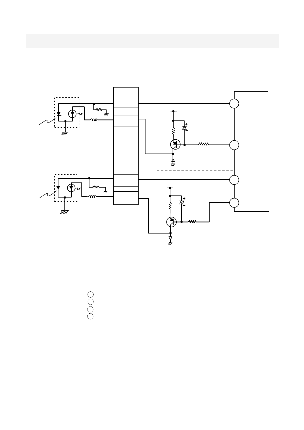
1-2. APC Circuit Operation
It controls the power of Laser Diode in the Optical Pick-up.
To get the constant and stable LASER power, it uses the Monitor Diode in the Optical Pick-up.
IC201 (TA1293F) Pin : MDI1 -- DVD Laser Monitor Input
: MDI2 -- CD Laser Monitor Input
IC201 (TA1293F) Pin : LDO1 -- DVD Laser control signal output
: LDO2 -- CD Laser control signal output
The detected current at the monitor diode is converted into voltage by I/V converter in the optical Pick-Up
and this becomes the input signal of MDI(Pin 59, 3).
In the RF AMP this signal is amplified about 270 times (48.7dB) and then outputs form LDO (Pin 60, 2)
and becomes the input of LD driving element (Q203 for DVD, Q205 for CD).
Q203 and Q205 are Transistors with 200hfe or more.
If DVD disc is loaded, only DVD APC System is operating and CD APC system is off by the command
from the µ-com and CD disc is loaded CD APC system only operating.
1. APC (Automatic Power Control) Circuit
1-1. APC Circuit Constitution
59
3
60
2
DESCRIPTION OF CIRCUIT
Page 4
12
60 59 58 57 56 55 54 53 52 51 50 49 48 47 46 45 44 43 42 41
40393837363534333231302928272625242322
21
2019181716151413121110987654321
80
79
78
77
76
75
74
73
72
71
70
69
68
67
66
65
64
63
62
61
P1TN
LDO1
MDI1
EQF
EQB
RFDC
GND2
EQD
NC
Vcc2
VccO
PSC
FEB
TEB
DPDB
VccR
RFO
RPP
RPB
RPO
RPZ
P1TP
P1FN
P1FP
LDP1
GNDR
P1DI
P1CI
P1BI
P1AI
LDP2
P2AI
P2BI
P2CI
P2DI
GNDS
P2FP
P2FN
P2TP
P2TN
GNDP
LDO2
MDI2
NC
NC
VrA
Vrfi
VrD
Vdd
DPAC
DPBD
DPD1
DPD2
SCB
SCL
SCD
VRCK
NC
NC
VccP
NC
NC
NC
NC
NC
NC
NC
NC
NC
NC
NC
NC
NC
DFTN
TEO
FEO
LVL
RFSW
VccS
VCKF
APC1
sel-RF
sel-PD
sel-PD
sel-PD
R-gain
Adjustment
sel-LVL
sel-TE2
sel-TE1
sel-FE
mode-RP
F-gain
Adjustment
F-gain
Adjustment
EQ
TEB
Generating
3BTE
T-gain
Adjustment
APC2
Vref
BUS
mode-TE
TE-gain
Adjustment
Level
Detection
Generating
DPDTE
TEB
DPDB
Generating
FE
FE-gain
Adjustment
Generating
RF Ripple
C001
C002
CN05 DVD-VCC
CN06 DVD-VC
CN07 DVD-PD-GND
CN09 DVD-A
CN11 DVD-B
CN12 DVD-C
CN08 DVD-D
CN17 DVD-VR
CN16 DVD-MD
CN13 DVD-LD
CN14 DVD-LD-GND
CN15 DVD-HFM
CN02 FO+
CN03 FO-
CN04 TR+
CN01 TR-
CN23 CD-VCC
CN22 CD-VC
CN21 CD-GND
CN27 CD-C
CN25 CD-B
CN24 CD-A
CN28 CD-D
CN30 CD-F
CN29 CD-E
CN18 CD-VR
CN19 CD-MD
CN20 CD-LD
C010
C011
C012
VR10
U002
U001
TRACKING
FOCUS
C003
C004
L002
L001
Actuator
VR01
LASER DIODE
Frequency
Superposition
circuit
Time Constant
Adjustment
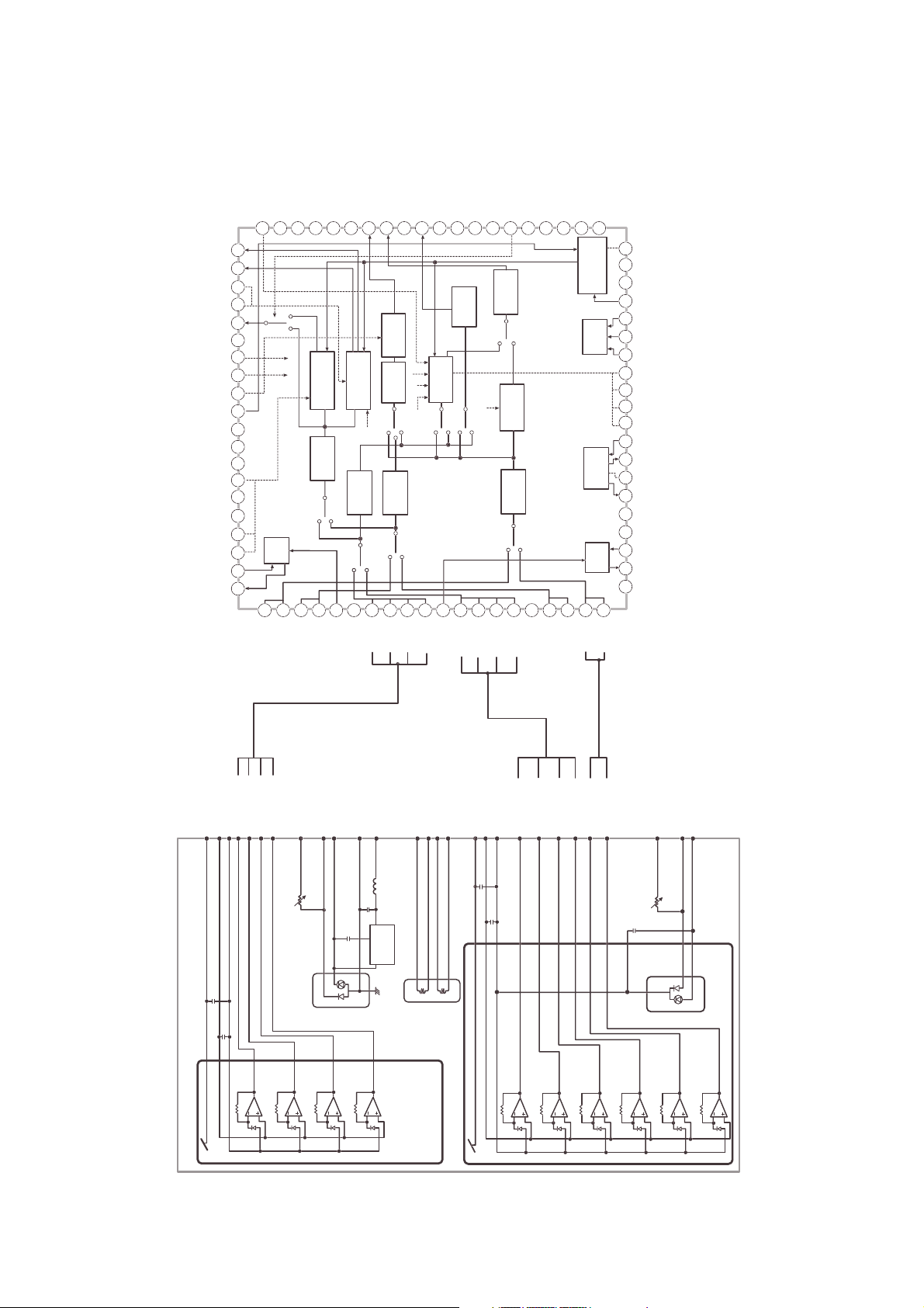
2. RF Amplifier Circuit
2-1. RF AMP Constitution
Page 5

13
2-2. RF AMP Circuit Operation
2
54
18
24
24
28
20
21
46
55
52
53
3
In the Optical Pick-Up, Photo Diode receives the reflected LASER beam from the Disc and makes it into
current . This current is converted into voltage by I/V Amp and input to RF AMP to make RF signal and
Servo signals.
Pick-Up unit has two LASER Diodes and Photo Diodes for CD and DVD respectively and they are
controlled by µ-com separately.
(1) CD (CD-DA, CD-ROM, VIDEO-CD, CD-R, CD-RW)
In DRN-8040B the hologram module is used for CD optical system and conventional type is used for
DVD optical system. There are 4 signals for CD Disc, they are A, B, E and F. (A+B) generate RF
signal, (B-A) is focus error signal and (E-F) is tracking error signal.
(2) DVD (DVD-Single layer, Dual layer, DVD-R)
For DVD RF and servo signals, we use 4 optical pick-up signals, A, B, C and D. RF is generated by
(A+B+C+D), Focus error is (A+C)-(B+D) and tracking error is the Phase difference of (A+C) and (B+D).
<Input and output signals RF Amp. (IC201)>
RF Amp (IC201 : TA1293F) has different input channels for CD and DVD.
The input terminals for CD disc are Pin 72(A), 73(B), 74(C), 75(D), 79(E) and 80(F).
For DVD, Pin 70(A), 69(B), 68(C), and 67(D) are used.
These Pick-Up signals are used for RF, Focus Error, Tracking Error and useful signals for stable
servo system. RF Amp has Gain amplifiers for each signals to adjust the level of signals and
µ-com control them by write the gain values into resisters in the RF Amp. (See the Fig.: TA1293F
internal block diagram)
To make good RF signal, we use three RF equalization terminals, they are EQB (Pin 57), EQF (Pin 58),
and EQD (Pin 54). Assigning the DC voltage to each terminal, DSP IC (TC9453F) control them.
EQB adjust the amount of RF boost, and EQF is frequency bandwidth of RF signal. EQD is fixed to Vref
(1.65V) now.
<Useful signals for stable Servo system>
LVL (Pin 31) : Sub beam add signal (E+F), this is used for FOK (focus OK) and defect signal.
RPO (Pin 42) : RF ripple signal (RF peck level-RF Bottom level) and using this DSP count the number
of crossed tracks.
RPZ (Pin 41) : Center level of RPO
RFO (Pin 45) : CD/DVD RF out.
TEO (Pin 33) : Tracking Error out.
FEO (Pin 34) : Focus Error out.
VRCK (Pin 17) : The reference signal for RF Equalization and Servo signals (it is variable to CD or DVD
and Speed of Disc)
Page 6
14
FOCUS & TRACKING SERVO PROCESS
SLED(Feed) SERVO PROCESS
F
E
A
A
B
B
A
B
D
A
C
B
Pick - Up
IC201
RF AMP
TA1293F
5
CD
B-A
A.B.C.D
E-F
(A+C)-(B+D)
(A. B. E. F)
4
DVD (A. B. C. D)
3B TE/
DPD TE
SELECTOR
FEO
Generating
DPD TE
Generating
3B TE
FOCUS
ERROR
DETECTOR
FOCUS &
TRACKING
ACTUATOR
IC601
DRIVE
BA5913FPY/
BA5918FPY
IC301
CD/DVD SERVO & DSP
TC9453F
F+ F-T+ T-
LEVEL SHIFT
LEVEL SHIFT
FOO
TRO
D/A
DIGITAL
EQUALIZER
(AUTO ADJUSTMENT
CIRCUIT)
SLED
Control
Signal
A/D
TE FE
TEO
FMO
SLED MOTOR
PHOTO
Interrupter
M
SL+
SL-
LEVEL SHIFT
IC601
DRIVE
BA5913FPY/BA5918FPY
+
IC501
u-COM
SLED CLOCK
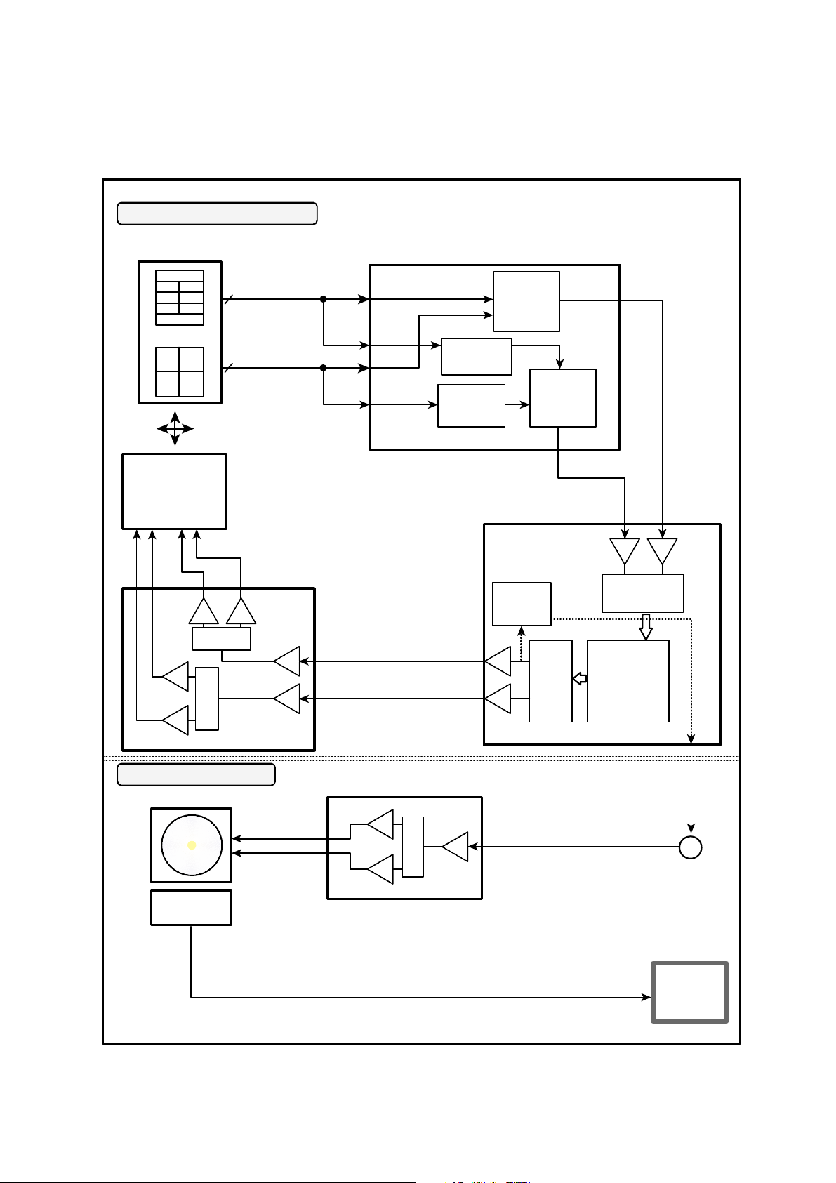
3. Focus/Tracking/Sled Servo Circuit
3-1. FOCUS, TRACKING & SLED SERVO PROCESS
Page 7

15
3-2. Focus Servo for CD/DVD
Focus Servo for CD/DVD is based on focus error signal generated from RF AMP (TA1293F). It standardizes the
laser beam (CD:A, B, DVD:A, B, C, D) radiated from the pick-up.
Each other focus gain is made at the TA1293F (IC201) according to the disc, Focus Error signal is
output from the FEO terminal and is input to Servo IC (IC401 TC9453F).
After the first amplification of this signal, the signal is converted to A/D and input to Digital Equalizer Block
and generates the focus servo ERROR signal with coefficient value is set at the µ-COM through the Digital
Filter.
At this Digital Equalizer, auto adjustment for Focus Balance or Focus Loop Gain occurs and the basic offset
value for pick-up is accepted on the balance mode, and set the focus standard level to this value.
After the signal for Focus Servo is converted to the D/A and output through FOO (IC401 TC9453F ).
This signal goes through LPF (R435, C426), drives Focus Actuator through the Focus Drive IC
(IC601:BA5918).
3-3. Tracking Servo for CD/DVD
For Tracking Servo, CD uses 3 Beam method (E-F), DVD uses DPD (Differential Phase Detect) method
(phase difference between A+C signal and B+D signal).
According to the disc, Tracking Error is set at TA1293F, Gain or Path differs from each other, and the
generated signal output through the TEO terminal.
This signal input to TEI of IC401, after the first amplification, and converted to A/D.
The signal converted to A/D input to the Digital Equalizer Tracking Servo Gain is generated with Digital Filter
coefficient value set according to the disc at the µ-COM.
* Tracking balances at this digital equalizer automatically, adjusted balance input to pin TEB terminal of
IC201 through the pin (TEBC) of IC401. Tracking Error Balance is adjusted, and the reference level for
the balance sets offset value to produce differently according to CD/DVD at the first disc drive.
Tracking signal is converted to D/A through the pin TRO terminal of IC401 and output is through
LPF (R436, C425), and input to IC601 (BA5913FP) tracking drive.
This drive drives the tracking actuator actually.
3-4. Sled Servo (Feed Servo) for CD/DVD
Sled servo operates related with a tracking servo basically
It goes with the progressive track speed according to the disc rotation speed.
Sled drive voltage is generated with a accumulated capacity of tracking error signal and is applied sled
movement voltage according to the track movement capacity, and this voltage outputs to the pin FMO of
IC401. This value is through LPF(R437, C424) and the sled motor drove by the IC601 (Sled drive:
BA5918FP).
158
164
162
48
159
Page 8
16
E
A
A
B
A
B
B
5
F
A
M
D
BC
PICK-UP
SPINDLE MOTOR ASSY
CD(A. B. E. F) A+B
CD RF
DVD RF
A+B+C+D
IC501
IC401
PLL BLOCK
FG
CD/DVD
RF
Motor
Hall Sensor
U
HU+
HUHV+
HVHW+
HW-
6
V
W
Speed
Monitoring
u-com
CD/DVD SERVO & DSP
TC9453F
IC201
RF AMP
TA1293F
4
DVD(A. B. C. D)
SPINDLE SERVO PROCESS
LEVEL SHIFT
AN8473SA
C423
R438
CAV DMO
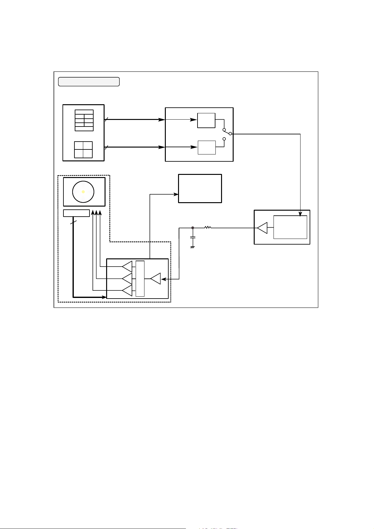
4. Spindle Servo Circuit
4-1. SPINDLE SERVO PROCESS
4-2. Spindle Servo for CD/DVD
DRN-8040B consists of the 3 spindle control respectively.
(1) DVD 4X : CAV (DVD signal & dual layer)
(2) CD 12X : CAV (CD-DA, CD-RW, Video-CD, Host command standby of CD-ROM)
(3) CD 24X : CAV (CD-ROM, CD-R, CD-R playback mode)
In the spindle speed control mode respectively.
DRN-8040B has only full CAV system in speed of DVD x4, CD x12 and CD x24.
In each speed mode, µ-com writes the sets of disc speed commands to DSP (IC401) resisters.
And these command sets and FG signal from the spindle motor determine the speed of disc automatically.
First, DSP (IC401) monitoring the FG signal of spindle motor through the Pin 175(FG), and compares it’s
duty (frequency) with desired speed mode in DSP resisters that is written by µ-com.
To make and sustain the each CAV Speed, DSP (IC401) controls the spindle motor by DMO (Pin 163)
signal.
This DMO signal goes to spindle motor drive IC and it’s output signals U, V and W drive the spindle motor.
In DVD x4, CDx12 and CDx24 CAV mode DSP (IC401) monitoring the FG signal of Spindle Motor and
control the speed of each mode by sets of coeffecients that
Page 9

22
IC201 (TA1293F) : RF Signal Processing for CD/DVD
It amplifies or equalize the RF signal from Pick-up, and generate the TE (Tracking Error) and FE
(Focus Error) signal for Servo respectively.
The TE signal uses the DPD (Differential Phase Detect) method for DVD and 3 Beam method for
CD.
DVD FE=(A+C)-(B+D)
CD FE=A-B
Block Diagram
60 59 58 57 56 55 54 53 52 51 50 49 48 47 46 45 44 43 42 41
40
39
38
37
36
35
34
33
32
31
30
29
28
27
26
25
24
23
22
21
2019181716151413121110987654321
80
79
78
77
76
75
74
73
72
71
70
69
68
67
66
65
64
63
62
61
P1TN
LDO1
MDI1
EQF
EQB
RFDC
GND2
EQDNCVcc2
VccO
PSC
FEB
TEB
DPDB
VccR
RFO
RPP
RPB
RPO
RPZ
P1TP
P1FN
P1FP
LDP1
GNDR
P1DI
P1CI
P1BI
P1AI
LDP2
P2AI
P2BI
P2CI
P2DI
GNDS
P2FP
P2FN
P2TP
P2TN
GNDP
LDO2
MDI2NCNC
VrA
Vrfi
VrD
Vdd
DPAC
DPBD
DPD1
DPD2
SCB
SCL
SCD
VRCKNCNC
VccP
NC
NC
NC
NC
NC
NC
NC
NC
NC
NC
NC
NC
NC
DFTN
TEO
FEO
LVL
RFSW
VccS
VCKF
APC1
sel-RF
sel-PD
sel-PD
sel-PD
R-gain
Adjustment
sel-LVL
sel-TE2
sel-TE1
sel-FE
mode-RP
F-gain
Adjustment
F-gain
Adjustment
EQ
TEB
Generating
3BTE
T-gain
Adjustment
APC2
Vref
BUS
mode-TE
TE-gain
Adjustment
Level
Detection
Generating
DPDTE
TEB
DPDB
Generating
FE
FE-gain
Adjustment
Generating
RF Ripple
Time Constant
Adjustment
MAJOR IC INTERNAL BLOCK DIAGRAM AND PIN DESCRIPTION
Page 10

I/O Description DC Voltage Remark
– GND –
O LD output –
I Monitor input –
–– –
–– –
O Analong V
REF 2.1[V]
– Filter for reference –
O Digital V
REF – 1/2 of Vdd
I Vdd – 3.3V
– DPD AC Capacitor 1 –
– DPD AC Capacitor 2 –
– DPD integral Capacitor 1 –
– DPD integral Capacitor 2 –
I Bitclock 2.2[V]
I Latch signal 2.2[V]
I Serial data 2.2[V]
If the frequency is up,
I Reference clock input 2.3[V] the filter shifts to high
frequency except for servo LPF.
–– –
–– –
– Time constant adjustment –
– VccP –
–– –
–– –
–– –
–– –
I RFO Control input –
– VccS –
–– –
–– –
–– –
O Servo Added output VrD X (1/2)
–– –
O TE Output VrD
O FE output VrD
–– –
–– –
–– –
–– –
–– –
23
Pin No.
1
2
3
4
5
6
7
8
9
10
11
12
13
14
15
16
17
18
19
20
21
22
23
24
25
26
27
28
29
30
31
32
33
34
35
36
37
38
39
Pin Name
GNDP
LDO2
MDI2
NC
NC
VrA
Vrfi
VrD
Vdd
DPAC
DPBD
DPD1
DPD2
SCB
SCL
SCD
VRCK
NC
NC
VCKF
VccP
NC
NC
NC
NC
RFSW
VccS
NC
NC
NC
LVL
NC
TEO
FEO
NC
NC
NC
NC
NC
• IC201 (TA1293F)
Pin Description
Page 11

24
I/O Description DC Voltage Remark
I DPD defect – Low: DPD output is Mute.
O RF ripple center VrD X (1/2)
O RF ripple output VrD X (1/2)
O RF ripple bottom –
O RF ripple peak –
O Equalising RF output 2.3[V]
– VccR (RF) –
I Pit deep Adjustment VrD
DPDB is up, A and B delay is up.
I TE balance VrD TEB is up, A+C Gain is up.
I FE balance VrD FEB is up, A+C Gain is up.
I VRCK ON/OFF – H: devide is off.
– VccO –
– Vcc2 –
–– VrD
I Group delay compensator VrD
EQD is up, Group delay is to right.
– GND –
– DC feedback capacitor –
I Boost Adjustment VrD EQB is up, Boost is up.
I Frequency Adjustment VrD EQF is up, frequency is
shifted to high frequency.
I Monitor input –
O LD Drive output –
I TE- input (DVD) VrA
I TE+ input (DVD) VrA
I FE- input (DVD) VrA
I FE+ input (DVD) VrA
I APC control 1 –
– GND –
I D input (DVD) VrA
I C input (DVD) VrA
I B input (DVD) VrA
I A input (DVD) VrA
I APC control 2 –
I A input (CD) VrA
I B input (CD) VrA
I C input (CD) VrA
I D input (CD) VrA
– GND –
I FE+ input (CD) VrA
I FE- input (CD) VrA
I TE+ input (CD) VrA
I TE- input (CD) VrA
Pin No.
40
41
42
43
44
45
46
47
48
49
50
51
52
53
54
55
56
57
58
59
60
61
62
63
64
65
66
67
68
69
70
71
72
73
74
75
76
77
78
79
80
Pin Name
DFTN
RPZ
RPO
RPB
RPP
RFO
VccR
DPDB
TEB
FEB
PSC
VccO
Vcc2
NC
EQD
GND2
RFDC
EQB
EQF
MDI1
LDO1
P1TN
P1TP
P1FN
P1FP
LDP1
GNDR
P1DI
P1CI
P1BI
P1AI
LDP2
P2AI
P2BI
P2CI
P2DI
GNDS
P2FP
P2FN
P2TP
P2TN
Page 12

25
• IC401 (TC9453F)
IC401 receives the RF output signal of IC201 demodulates EFM, transfer to IC701 (TC9469AF), and
converts the analog audio signal output through the D/A convertor. RF, TE and FE signal of IC201,
related to servo, passes through the servo circuit of IC401, outputs the control signal to PWM or
D/A, and are transferred to Drive IC for the most desired servo.
Block Diagram
ADC
Digital
Servo
DSP
Output
I/F
from
RF-Amp.
(Servo signal)
from
RF-Amp.
(RF signal)
PLL
RF Signal
Process
Sync
ECC
MPU I/F
1Mbit
DRAM
MPU
Data Out
Output
I/F
Clock
PLL
1bit DAC
for CD-DA
to Driver
DigitalINAnalog
Out
Page 13

26
I/O Description 3V or 5V Remark
–––
– DAC GND only ––
O R-ch output 3V Analog output
– DAC power only 3V –
O AMP reference output 3V Analog input
O L-ch output 3V Analog output
– DAC GND only ––
– GND for oscillator ––
I X-tal input 3V Analog input
O X-tal output 3V Analog output
– Power for oscillator ––
– Test pin 3V GND
– Test pin 3V OPEN
– Test pin 3V VDD3
– 3.3V digital power ––
– 3.3V digital GND ––
O
Analog PLL Phase/frequency compare output
3V Analog output
I Test mode Pin 3V VDD3
I VCO Filter input for PLL clock 3V Analog input
O VCO Filter output for PLL clock 3V Analog output
– 3.3V digital GND ––
O Monitor for Test 3V
– 3.3V digital power ––
–––
I Test mode pin 3V VDD3
I/O Flag monitor A 5V
I/O Flag monitor B 5V
– 3.3V digital GND ––
I RESET 5V
I Micom address enable 5V
I Micom data read 5V
I Micom data write 5V
Pin No.
1
2
3
4
5
6
7
8
9
10
11
12
13
14
15
16
17
18
19
20
21
22
23
24
25
26
27
28
29
30
31
32
33
34
35
36
37
38
39
40
41
42
43
Pin Name
NC
NC
DVSS
RO
DVDD
DVR
LO
DVSS
XVSS
XI
XO
XVDD
TESM0
TESM1
TESM2
VDD3
VSS3
VPFC
TEST0
VLPFI
VLPFO
VSS3
MON0
MON1
MON2
MON3
MON4
MON5
MON6
MON7
MON8
MON9
VDD3
NC
NC
TEST1
FLGA
FLGB
VSS3
/RST
/MA
/MRD
/MWR
• IC401 (TC9453F)
Pin Description
Page 14

27
I/O Description 3V or 5V Remark
I Micom chip enable 5V
O Micom interrupt signal 5V
I/O Micom data-bus 5V
– 5V power ––
––
O 22M clock output 5V
O Clock output for signal processing 5V
– 3.3V digital power ––
O DVD/CD data output 5V
– 5V GND ––
O DVD/CD data output 5V
– 3.3V digital GND ––
O DVD/CD data output 5V
O DVD data sector SYNC signal 5V
O DVD data transfer block 5V
O DVD data transfer clock 5V
– 5V power ––
– Test pin 5V VSS5
I 1BitDAC digital IN input 5V
– TEST 5V VDD5
– 3.3V digital power ––
O RAM address output 5V
– 5V GND ––
O RAM address output 5V
Pin No.
44
45
46
47
48
49
50
51
52
53
54
55
56
57
58
59
60
61
62
63
64
65
66
67
68
69
70
71
72
73
74
75
76
77
78
79
80
81
82
83
84
85
86
87
88
Pin Name
/MCE
/MINT
MD0
MD1
MD2
MD3
MD4
MD5
MD6
MD7
VDD5
NC
NC
SMCK
VMCK
VDD3
PD0
VSS5
PD1
PD2
PD3
PD4
VSS3
PD5
PD6
PD7
PD8
/PSYC
/PDRQ
PDCK
VDD5
TESM3
DIGI
TESM4
VDD3
BA0
BA1
BA2
BA3
VSS5
BA4
BA5
BA6
BA7
BA8
Page 15

28
I/O Description 3V or 5V Remark
– 3.3V Digital power ––
O RAM/OE signal 5V
O RAM/RAS signal 5V
O RAM/CAS signal 5V
O RAM Lower/WE signal 5V
O RAM Upper/WE signal 5V
– 5V Power ––
I/O RAM data in/output 5V
I/O RAM data in/output 5V
I/O RAM data in/output 5V
– 3.3V digital GND ––
I/O RAM data In/output 5V
– 5V GND ––
– RAM dataIn/output 5V
––
– 3.3V digital power ––
I/O PLL clock In/output 3V
– Test pin 5 3V GND
– Test pin6 3V GND
– Test pin7 3V OPEN
– Test pin8 3V OPEN
– 3.3V digital GND ––
O VCO frequency control signal 1 3V
O VCO frequency control signal 2 3V
O Offset adjustment output for phase comparator 3V
I Offset adjustment input for phase comparator 3V
– 3.3V PLL GND only ––
O Offset adjustment signal output 3V
O DVD/CD phase control signal 1 (positive) 3V
O DVD/CD phase control signal 1 (negative) 3V
O DVD/CD phase control signal 2 (positive) 3V
O DVD/CD phase control signal 2 (negative) 3V
Pin No.
89
90
91
92
93
94
95
96
97
98
99
100
101
102
103
104
105
106
107
108
109
110
111
112
113
114
115
116
117
118
119
120
121
122
123
124
125
126
127
128
129
130
131
132
133
Pin Name
VDD3
/BOE
/BRAS
/BCAS
/BWL
/BWU
VDD5
BD0
BD1
BD2
BD3
BD4
BD5
BD6
BD7
BD8
VSS3
BD9
BD10
BD11
BD12
VSS5
BD13
BD14
BD15
NC
NC
VDD3
PLCK
TESM5
TESN6
TESM7
TESM8
VSS3
CFC1
CFC2
PPW
PESV
PVSS
PESP
PDOP1
PDON1
PDOP2
PDON2
LPFN
Page 16

29
I/O Description 3V or 5V Remark
O Data PLL output 3V
– Data PLL reference voltage 3V
I VCO reference 3V
I VCO auto adjustment filter 3V
– 3.3V PLL power only ––
O Data slice 6bitDAC output 3V
– Test pin9 3V OPEN
I Test mode 2 3V VDD3
I CD RF input 3V
I DVD RF input 3V
– 3.3V analog power ––
I RFRP center voltage 3V
I RFRP input 3V
I Tracking error input 3V
I Active wide PLL input 3V
– 3.3V GND ––
I Focus error input 3V
I Tracking error input 3V
I RF level input 3V
I RFRP input 3V
– 3.3V GND ––
– Test pin10 3V VREF
I General exfernal ADC input 3V
– Reference voltage : 1.65V 3V
O Focus EQ ouput 3V
O Tracking EQ output 3V
– 3.3V analog power ––
O Active wide PLL output 3V
O Focus EQ output 3V
O Disc EQ output 3V
O Tracking balance control 3V
O Focus balance control 3V
O DPD control 3V
O EQ balance control 3V
O PWM output 3V
O Black dot detect 3V
O RF EQ control clock 3V
– 3.3V digital GND ––
O Serial data
O Serial catch 3V
O Serial clock 3V
I FG input 3V
––
Pin No.
134
135
136
137
138
139
140
141
142
143
144
145
146
147
148
149
150
151
152
153
154
155
156
157
158
159
160
161
162
163
164
165
166
167
168
169
170
171
172
173
174
175
176
Pin Name
LPFO
PVREF
VCOREF
VCOF
PVDD
SLCO1
TESM9
TEST2
RFCD
RFDVD
AVDD
RFCT
RFZI
TEZI
AWIN
AVSS
FEI
TEI
RFSB
RFRP
AVSS
TESM10
EXTAD
VREF
FOO
TRO
AVDD
AWCTL
FMO
DMO
TEBC
FEBC
DPDC
EQBC
ANMON
/DFCT
VRCK
VSS3
SCD
SCL
SCB
FGIN
NC
Page 17

30
• IC701 (TC9469AF) : Enhanced IDE Interface CD/DVD ROM Decoder
• It is a CD/DVD Decoder enhanced the IDE rated interface.
• Data of DVD Disc is transferred.
• Confirmation management
• Correspond to Max 32X CD DISC
Block Diagram
64
DRAM 256kW / 128 kW / 64 kW
(4Mbit / 2Mbit / 1Mbit)
BD15-0
/BWU, /BWL
/BOE
/RAS, /CAS
/BA8-0
8
16
16
3
16
64
64
16
16
8
16
89
8
3
2 9
2
2
5
16
CSEL
(H-IF)
H-FIFO
ECC
Buffer
(64B)
/PDIAG, /DASP
IORDY
HDRQ
/IOCS16
HD15-O
/HRD, /HWR
/HCS3, /HCS1
HA2-0
INTRQ
DIGO
ASYC
BSYC
SBDa
SBQa
HSYC
Da
Daf
HEDda
PSYCN, PDRQN
PDCK
SEDVD
PDA8
/RST
XI
X0
Gnd
Vdd
TEST2-0
30
3
8 3 7
8
8
PDA (7 : 0)
/MINT
MA6-0
/MCE
MD7-O
/MWR, /MRD
AV-IF
M-FIFO
AUTH
SUB-IF
Input
conversion
Input
select
CD-IF &
Buffer
DVD-IF
EDC
(88 x 3ch)
(M-IF)
Clock
TC9469F
AZCK
ABCK, ACHCK
ADO
/HDAK
3
Compensation
M
AddressHInterrupt
H
Interrupt
µ-COM
Driver
Page 18

31
I/O Description Remark
– –
– GND –
Host address 2 input
I Chip select 1 input TTL level
Chip select 3 input
I/O Drive active in/output TTL level
I General purpose PIO terminal –
– GND –
– Power supply terminal –
I/O Buffer RAM data In/output Low power:output
– Power supply terminal –
– GND –
I/O Buffer RAM data In/output Low power: output
– GND –
O
High position 8bit write enable Low power: H
(For CAS signal high position 8bit on 2 CAS type)
O
High position 8bit write enable Low power: H
(wrtie enable on 2 CAS type)
O CAS signal output
Low power: H
(For CAS signal low position 8bit on 2 CAS type)
O RAS signal output Lowpower:H
O Output enable terminal Lowpower:H
O Buffer address output –
– Power supply terminal –
– –
– –
– GND –
Pin No.
1
2
3
4
5
6
7
8
9
10
11
12
13
14
15
16
17
18
19
20
21
22
23
24
25
26
27
28
29
30
31
32
33
34
35
36
37
38
Pin Name
NC
VSS
HA2
/HCS1
/HCS3
/DASP
CSEL
VSS
VDD
BD15
BD14
BD13
BD12
BD11
BD10
BD9
BD8
VDD
VSS
BD4
BD5
BD7
BD6
BD3
BD2
BD1
BD0
VSS
/BWU
/BWL
/CAS
/RAS
/BOE
BA8
VDD
NC
NC
VSS
• IC701 (TC9469AF)
Pin Description
Page 19

32
I/O Description Remark
O Buffer address output –
– GND –
O Buffer address output –
I Test terminal, Fixed “L”–
– GND –
I
Master clock In/output –
O
– Power supply terminal –
O Digital out –
– –
I Data read clock input –
I Data flag input –
SYNC input
At CD disc
–
I
I Parallel data 8 input –
I Parallel data 7 input –
I Parallel data 6 input –
I Parallel data 5 input –
– GND –
I Parallel data 4 input –
I Parallel data 3 input –
I Parallel data 2 input –
I Parallel data 1 input –
Pin No.
39
40
41
42
43
44
45
46
47
48
49
50
51
52
53
54
55
56
57
58
59
60
61
62
63
64
65
66
67
68
Pin Name
BA7
BA6
BA5
BA4
BA0
VSS
BA2
BA1
BA3
TEST0
TEST1
TEST2
VSSck
XI
XO
VDDck
DIGO
NC
PDCK
PDRQN
PSYCN
PDA8
PDA7
(SBSY)
PDA6
(SFSY)
PDA5
(SBDI)
VSS
PDA4
(CLCK)
PDA3
(C2PI)
PDA2
(DAI)
PDA1
(BCKI)
PDA8 PDA7 PDA6-0
PSYCN=0
Sub S0 SYNC 1 0
Sub S1 SYNC 1 1
Sub data 0 Sub data (P-W)
PSYCN=1
Data C2PN data [7(MSB bit):0]
Page 20

I/O Description Remark
I Parallel data 0 input –
– GND –
– –
– –
– –
I Reference input for audio playback –
O Bit clock output for audio playback –
O Audio data output –
O Channel clock (LRCK) output for audio playback –
– Power –
Select IF input
I 0: serial inferface –
1: parallel inferface
– GND –
I/O Micom data In/output 3 state output
– GND –
– Power supply terminal –
I Micom address input –
I Chip enable signal input –
Micom chip read signal input –
– GND –
I Micom write signal input –
O
Micom interrupt signal output
(Open drain output, enhanced pull-up resistor)
–
O TEST –
I H/W reset signal input
– Power supply terminal –
– GND –
– GND –
– –
– Power supply terminal –
Pin No.
69
70
71
72
73
74
75
76
77
78
79
80
81
82
83
84
85
86
87
88
89
90
91
92
93
94
95
96
97
98
99
100
101
102
103
104
105
106
107
108
109
Pin Name
PDA0
(LRCK)
VSS
NC
NC
NC
AZCK
ABCK
ADO
ACHCK
VDD
SEDVD
VSS
MD0
ND1
MD2
MD3
MD4
MD5
MD6
MD7
VSS
VDD
MA0
MA1
MA2
MA3
MA4
MA5
MA6
/MCE
/MRD
VSS
/MWR
/MINT
TESTOUT
/RST
VDD
VSS
VSS
NC
VDD
33
Page 21

I/O Description Remark
TTL Level
I/O Host data In/output [0~15] – input
– Open drain output
– Hi-Z (reset)
– GND –
I/O Host data In/output [0~15] TTL Level
– Power supply terminal –
– GND –
I/O Host data In/output
O Data request output 3-state output
I Host write signal input TTL Level
– GND –
I Host read signal Input TTL Level
– GND –
O IO transfer ready output 3-state output
– Power supply terminal –
– GND –
I Data acknowledge Input TTL Level
O Interrupt signal output
O Data bit wide select output
I Host address 1 input TTL Level
I/O Host diagnostic In/output TTL Level
I Host address 0 Input TTL Level
– Power supply terminal –
– –
Pin No.
110
111
112
113
114
115
116
117
118
119
120
121
122
123
124
125
126
127
128
129
130
131
132
133
134
135
136
137
138
139
140
141
142
143
144
Pin Name
HD7
HD8
HD6
HD9
HD5
HD10
VSS
HD4
HD11
HD3
HD12
HD2
HD13
HD1
HD14
HD0
VDD
VSS
HD15
HDRQ
/HWR
VSShr
/HRD
VSS24
IORDY
VDD24
VSS
/HDAK
INTRQ
/IOCS16
HA1
/PDIAG
HA0
VDD
NC
34
Page 22

35
• IC601 (BA5913FP) : Focus/Tracking/SLED Control Drive IC
Block Diagram
+
-
123456 78910111213
-
-
+
-
-
+
-
+
+
-
+
+
-
+
+
-
+
-
-
+
-
+
-
+
10K
10K10K
10K
10K
10K
10K 10K
10K 10K
10K
10K 10K
10K
10K
10K
10K
10K
10K
10K
10K
10K
Vcc
Vcc
25 24 23 22 21 20 19 18 17 16 15 14
STBY
LEVEL
SHIFT
LEVEL
SHIFT
LEVEL
SHIFT
LEVEL
SHIFT
Pin No.
1
2
3
4
5
6
7
8
9
10
11
12
13
Pin No.
14
15
16
17
18
19
20
21
22
23
24
25
Function
Vcc
Bias amplifier input
Driver CH1 input
Driver CH2 input, gain adjustment pin
Driver CH2 input
Substrate Ground
Substrate Ground
Input for stand-by control
Vcc
Driver CH2 inverted output
Driver CH2 noninverted output
Driver CH1 inverted output
Driver CH1 noninverted output
Functio
Driver CH4 noninverted output
Driver CH4 inverted output
Driver CH3 noninverted output
Driver CH3 inverted output
Vcc
Substrate Ground
0p-amp input, positive
0p-amp input, negative
0p-amp output
Driver CH3 input
Driver CH3 input,gain adjustment pin
Driver CH4 input
Pin Name
VCC
BIAS.IN
VIN1
VIN2
VIN2
GND
GND
STBY
Vcc
V02(-)
V02(+)
V01(-)
V02(+)
Pin Name
V04(+)
V04(-)
V03(+)
V03(-)
Vcc
GND
0P IN (+)
0P IN (-)
0P OUT
VIN3
VIN3
VIN4
Pin Description
* Symbol of + and - (output of DRIVERS) means polarity to input pin.
(For example if voltage of pin 3 is high, pin 13 is high.)
Page 23

1. CABINET
A. Release 3 screws (A).
B. Lift up the Cabinet in the direction of arrow (1).
(See Fig.1)
2. MAIN CIRCUIT BOARD
A. Inset and press a rod in the Emergency Eject Hole and
then the CD Tray will open in the direction of arrow (2).
B. Release 2 screws (B).
C. Remove the Main Circuit Board.
3. FRONT PANEL
A. Release 2 screws (C) and remove the Front Panel.
B. At this time, be careful not to damage the 2 hooks (a) of
the it. (See fig.3)
C. Release 3 screws (D) and remove the Cover Bottom (3).
4. BASE PICK-UP
A. Remove the Base Pick-up (4).
DISASSEMBLY
5
(1)
(A)
(A)
(A)
CABINET
2 HOOKS
HOOK (a)
FRONT PANEL
COVER BOTTOM
BASE PICK-UP
MAIN CIRCUIT BOARD
Emergency Eject Hole
Fig.1
Fig.3
Fig.2
Fig.4
(B)
(B)
(2)
(3)
(D)
(D)
(C)
(D)
(C)
(2)
(4)
Page 24

36
ABCD
1
2
3
4
5
Spindle
motor
Drive
AN8473SA
RF
Amplifier
TA1293F
Focus
actuator
Drive
Tracking
actuator
Drive
Slide
motor
Drive
BA5918FP
SF-HD4M
ATAPI
Interface
System
Controller
H8/3062F
TC9469AF
CD/DVD
Servo & DATA
PROCESSOR
DVD-ROM
Decoder & CSS
Audio
Signal
Processor
HOST COMPUTER
085125NE
Optical
Pick-up
Slide
motor
24C6988010
Spindle
motor
TC9453F
BLOCK DIAGRAM
Page 25

6
PBM00(MAIN C.B.A)
ABCD
1
2
3
4
5
436
436
436
001
012
011
013
006
007
008
010
009
435
435
435
435
435
436
436
005
004
003
A01
A00
EXPLODED VIEW
 Loading...