

Page 1

3
INTRODUCTION
GENERAL FEATURE
SPECIFICATIONS
1. SUPPORTED SYSTEM
¥ IBM Compatible Pentium 133MHz or Above (with PIO mode 4, TX chip set recommended)
2. SUPPORTED OS
3. GENERAL PERFORMANCE
¥ Data Transfer Rate ...........................................................................................Sustained Data Transfer Rate
DVD (Outer side) : Approx. 5,400 kbytes/sec
DVD (Inner side) : Approx. 2,700 kbytes/sec
CD (Outer side) : Approx. 4,800 kbytes/sec
CD (Inner side) : Approx. 2,100 kbytes/sec
¥ Data Buffer Capacity.......................................................................................................................512 kbytes
¥ Access Time..................................................................Random Access DVD : 130ms Typical (4X)
CD : 90ms Typical (32X)
4. POWER REQUIREMENTS
¥ Voltage ........................................................................................................................................+5V DC +5%
+12V DC +5%
¥ Ripple .....................................................................................................................................+5V : 100mVp-p
+12V : 100mVp-p
¥ Current .........................................................................................+12V : 400mA (Average), 0.9A (Maximum)
+5V : 500mA (Average), 1.2A (Maximum)
5. AUDIO PERFORMANCE
¥ Frequency Response.......................................................................................................20Hz~20KHz(+3dB)
¥ S/N Ratio (IHF-A+20kHZ LPF) ..........................................................................85 dB (Typical at 1 KHz 0dB)
80 dB (Limit at 1 KHz 0dB)
¥ T.H.D. (IHF-A+20kHZ LPF)...............................................................................0.05% (Typical at 1 KHz 0dB)
0.15% (Limit at 1 KHz 0dB)
¥ Channel Separation (IHF-A+20kHZ LPF) .................................................................................75 dB(Typical)
70 dB(Limit)
¥ Output Voltage (1kHz 0dB) 47K½ Load ..................................................................................0.8Vrms +20%
¥ Headphone Level (1kHz 0dB) 33½ Load.................................................................................0.6Vrms +20%
¥ Enhanced IDE interface
¥ Internal 5.25 inch, halfheight DVD-ROM Drive
¥ 130ms (Typical) Random Access Time (DVD)
¥ 90ms (Typical) Random Access Time (CD)
¥ Supports 4X (max) Rotational Modes in DVD Mode
¥ Supports 32X (max) Rotational Modes in CD Mode
¥ Max 5,400 kB/sec Sustained Transfer rate in DVD mode
¥ Max 4,800 kB/sec Sustained Transfer rate in CD mode
¥ Photo-CD Multisession Disc Spec compliant
¥ Multimedia MPC-3 Spec compliant
¥ Power Tray Loading/Ejection Mechanism
¥ 3-Way Eject Support (Software, Open/Close Button,
Emergency Eject)
¥ Closed Enclosure
¥ Built-in ATAPI Interface Controller
¥ Software Volume Control
¥ Easy CD-Audio Play front panel Controls
¥ Front panel Volume Control for Headphone Output
¥ Built-in MODE-1 ECC/EDC
¥ MTBF (125,000H) POH (at 10% Utilization)
¥ PIO Mode 4 & Multiword DMA Mode 2 Support
¥ Horizontal/Vertical Mounting
¥ Digital audio output connector
¥ Digital audio through ATAPI Interface
¥ Spin-down Mode for energy saving
¥ MS-DOS (Ver 3.1 or Higher)
¥ Windows 3.1/95/98
¥ Windows NT (Ver 4.0)
¥ OS/2 Warp (Ver 3.0)
¥ Solaris (Ver 2.4 or Higher)
¥ Linux Õ96 Slacware (Ver 3.1.0)
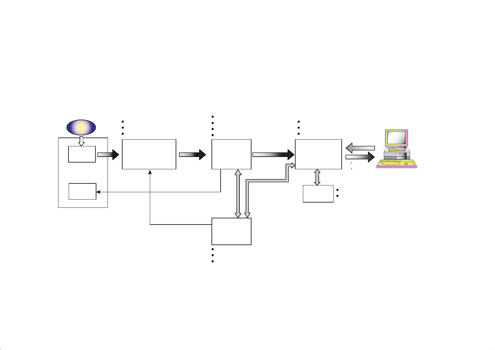
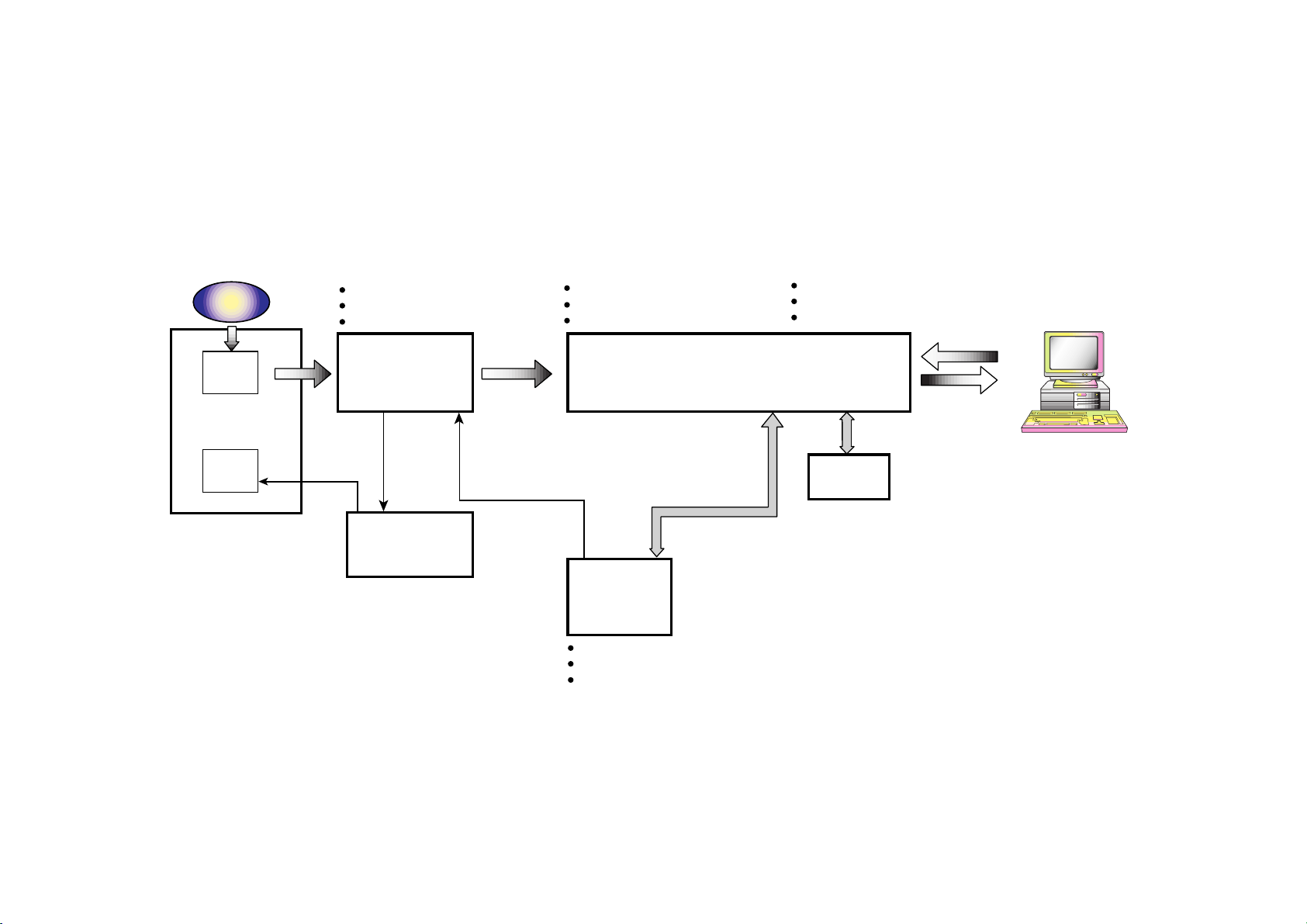
This service manual provides a variety of service
information. It contains the mechanical structure of
the DVD-ROM Drive together with mechanical
adjustments and the electronic circuits in schematic
form. This DVD-ROM Drive was manufactured and
assembled under our strict quality control standards
and meets or exceeds industry specifications and
standards.
Page 2

4
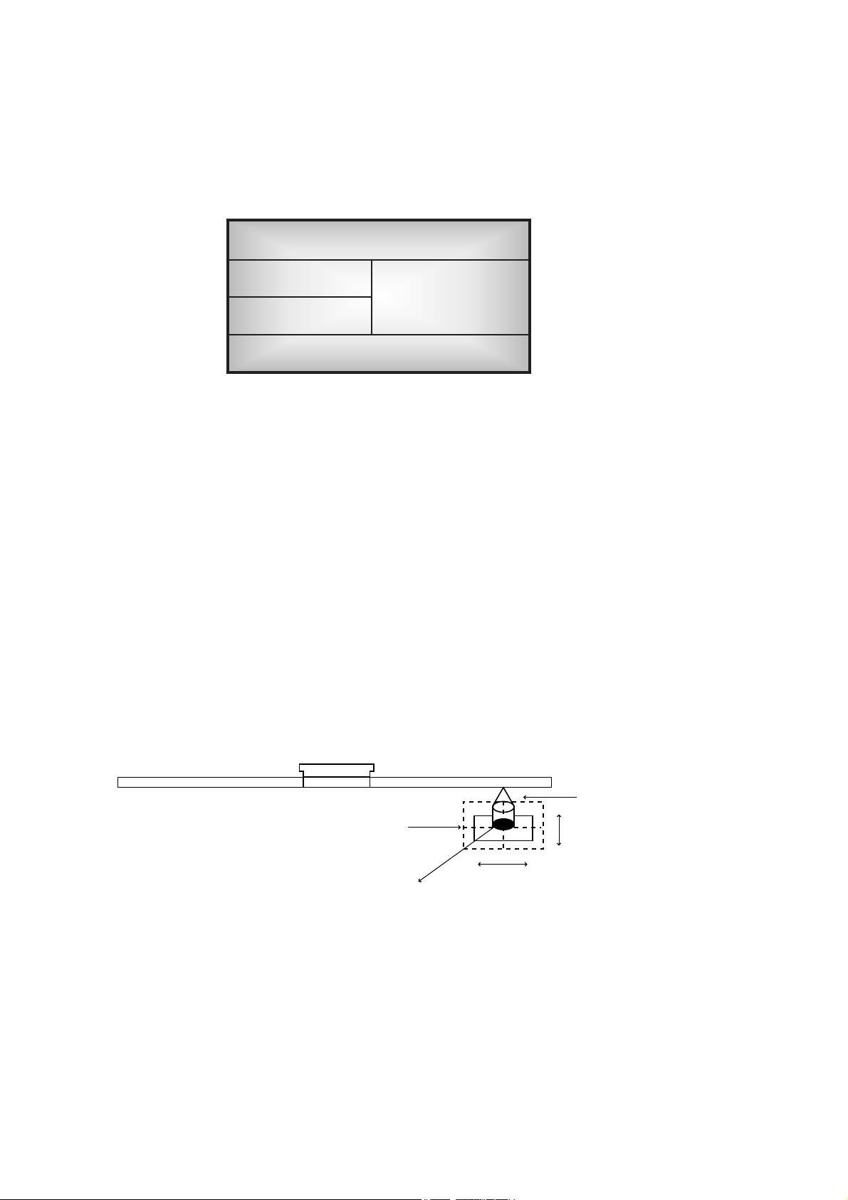
LOCATION OF CUSTOMER CONTROLS
(1) Digital Audio Ouput Connector
This is a digital audio output connector or Video CD
output connector.
You can connect this to the digital audio system or
Video CD Board.
(2) Analog Audio Output Connector
The Audio Output Connector connects to a sound
card.
The supplied audio cable is a SoundBlaster®type
cable. If you have a different sound card, you will
need to contact the sound card manufacturer to
obtain the proper cable for that card. This CABLE is
necessary to play audio CD’s.
(3) Master/Slave/CSEL Jumper
These three jumpers are used to set the DVD-ROM
Drive to either a Master, Slave, or CSEL drive.
(4) Interface Connector
This 40-pin connector is used to transfer and control
signals between the DVD-ROM Drive and your PC.
Connect the 40-pin IDE cable in your PC to this
connector.
(5) Power-in Connector
Attach a power cable from the computer’s power
supply to this connector.
COMPACT
DVD
DVD
BUSY
BUSY
ROM
DIGITAL ANALOG
INTERFACE POWER
DR CSM
SLA
GLG39 1
+5
+12
GND
40 2
AUDIO AUDIO
FRONT VIEW
BACK VIEW
(1) Headphone Jack
3.5mm jack for monitoring the audio signal from audio
CDs.
(2) Headphone Volume Control
Adjusts the headphone sound level.
(3) Emergency Eject Hole
Insert a paper clip here to eject the drawer manually or
when there is no power.
(4) DVD Indicator
The DVD Indicator lights during DVD disc data-read
operations.
(5) Busy Indicator (DVD, CD)
The Busy Indicator flickers during initialization and
data-read operations.
(6) Disc Drawer
Accepts a CD-ROM/DVD-ROM disc on its tray.
(7) Play/Skip Button
When an Audio CD is in the Disc Drawer, pressing
this button will start playing audio CDs from the first
track. If an audio CD is playing, pressing this button
will skip to the next track.
(8) Open/Close/Stop Button
This button is pressed to open or close the CD tray.
The button works only when the main power switch is
on.
If an audio CD is playing, pressing this button will stop
it, and pressing it again will open the tray.
Page 3
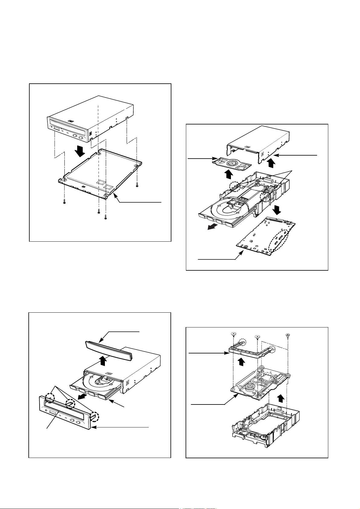
1. CABINET and CIRCUIT BOARD
DISASSEMBLY
1-1. Bottom Mecha
A. Release 4 screws (A) and remove the Bottom Mecha
in the direction of arrow (1). (See Fig.1-1)
1-2. Front Bezel Assy
A. Insert and press a rod in the Emergency Eject
Hole and then the CD Tray will open in the direction
of arrow (2).
B. Remove the Tray Door in the direction of arrow
(3) by pushing the stoppers forward.
C. Release 3 stoppers and remove the Front Bezel Assy.
1-3. Cabinet and Main Circuit Board
A. Remove the Cabinet in the direction of arrow (4).
(See Fig. 1-3)
B. Release 4 hooks (a) and remove the Clamp in the
direction of arrow (5).
C. Remove the CD Tray drawing forward.
D. Remove the Main Circuit Board in the direction of
arrow (6).
E. At this time, be careful not to damage the 4
connectors, are positioned at right side, of the Main
Circuit Board.
2. DECK ASSY DISASSEMBLY
2-1. Base Assy
A. Release 2 screws (C) and 2 Stoppers (D).
B. Separate the Base Assy in the direction of arrow (7).
C. Release 2 screws (E) and remove the Frame Assy
Up/Dowm.
(4)
(6)
(5)
Main
Circuit Board
Hooks(a)
Clamp
Cabinet
(A)
(A)
(A)
(A)
(1)
Fig. 1-1
Fig. 1-2
DISASSEMBLY
5
Fig. 1-3
Tray Door
Stoppers
CD Tray
Emergency Eject Hole
Front Bezel Assy
Bottom Mecha
(7)
(8)
(E)
(D)
(D)
(E)
(C)
Fig. 1-4
Base Assy
Frame Assy
Up/Down
(3)
(2)
Page 4

2-2. Pick-up Unit
A. Remove the skew spring.
B. Remove the Pick-up Unit.
2-3. Feeding Motor Assy
A. Remove the Feeding Motor Assy by pushing the 2
hooks(b).
B. At this time, be careful the hooks of the Base Pick-up.
6
Fig. 1-5
Fig. 1-6
Pick-up Unit
Skew Spring
Feeding Motor Assy
Base Pick-up
Hooks(b)
Page 5
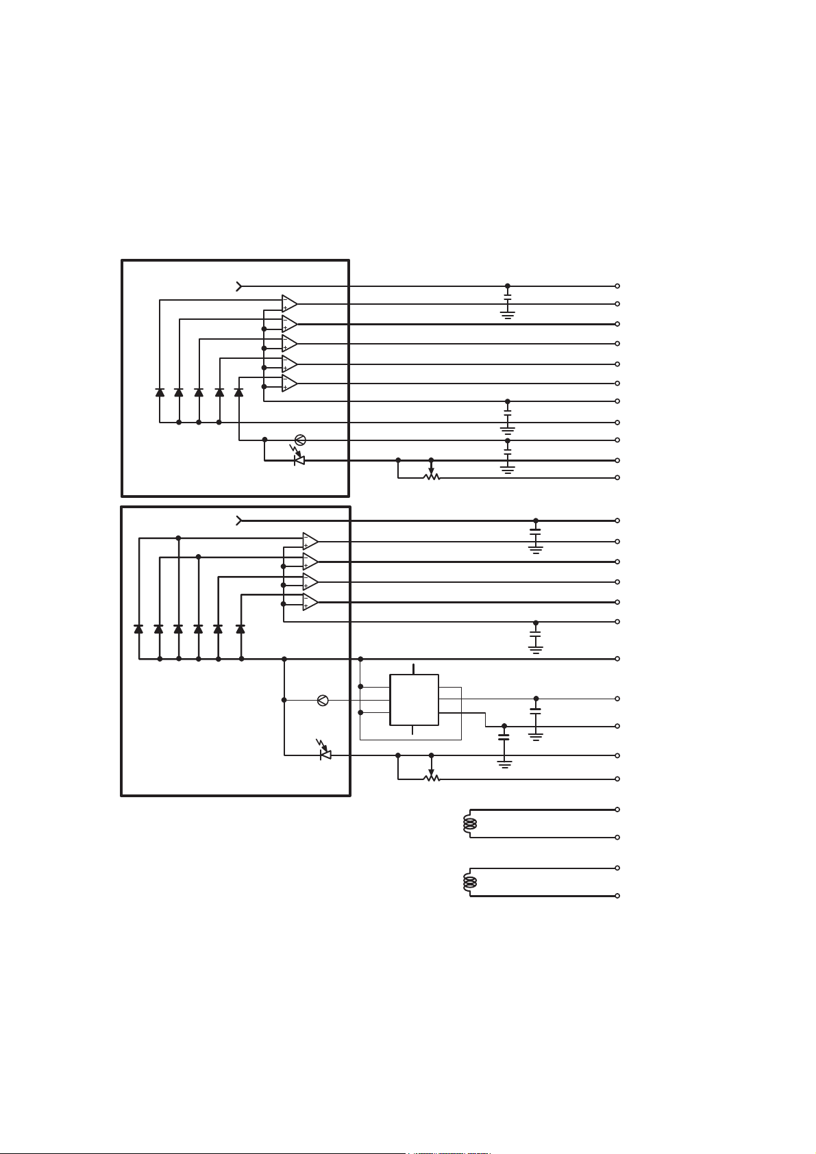
INTERNAL STRUCTURE OF THE PICK-UP
1. Structure of the Pick-Up
10
F-COIL
T-COIL
F+
F-
T-
T+
5K VOLUME
1.5K VOLUME
0.1u
0.1u
1u
0.1u
0.1u
0.1u
1u
HF MODULE
LD (DVD)
LD (CD)
MONITOR
PD(DVD)
MONITOR PD(CD)
PHOTO DETECTOR (DVD)
PHOTO
DETECTOR (CD)
< for CD >
< for DVD >
D2
D1 D2 D3 D4 D9
D10
D3 D4 D1 D5
7
6
5
G3 G1
I-IN
LD
G2
NC2
NC1
VCC
1
2
3
VCC (CD)
A (CD)
B (CD)
C (CD)
E (CD)
F (CD)
1/2VCC (CD)
GND (CD)
LD (CD)
MO-PD (CD)
VR (CD)
VCC (DVD)
A (DVD)
B (DVD)
E (DVD)
F (DVD)
1/2VCC (DVD)
GND(DVD)
LD(DVD)
HF (+5V)
MO-PD (DVD)
VR (DVD)
PN301-3
PN301-9
PN301-10
PN301-7
PN301-8
PN301-11
PN301-4
PN301-6
PN301-5
PN301-2
PN301-1
PN301-30
PN301-25
PN301-24
PN301-26
PN301-27
PN301-29
PN301-23
PN301-22
PN301-20
PN301-19
PN301-18
PN301-16
PN301-15
PN301-13
PN301-14
8
4
Page 6
11
1) Focus Error Signal Ð> A - B
¥ In case of CD Disc
This signal is generated in RF AMP IC (IC301 : SSI3721) and controls the pick-upÕs up and down to
focus on CD Disc.
2) Tracking Error Signal (3-Beam Method) Ð> E - F
¥ In case of CD Disc
This signal is generated in RF AMP IC (IC301 : SSI3721) and controls the pick-upÕs left and right shift to
find the track on CD Disc.
3) RF Signal Ð> A+B+2C
¥ In case of CD Disc
This signal is converted to DATA signal in DSP IC (IC701 : CXD3011R-1).
2. Structure of the Photo Diode (CD)
Infrared laser
Pick-Up module
Photo Diode
Tracking
Focusing
(As seen from light
receiving side)
E
C
B
F
A
Page 7
12
1) Focus Error Signal Ð> B - A
¥ In case of DVD Disc
This signal is generated in RF AMP IC (IC301 : SSI3721) and controls the pick-upÕs up and down to
focus on DVD Disc.
2) Tracking Error Signal (DPD Method) Ð> Phase (F) - Phase (E)
¥ In case of DVD Disc
This signal is generated in RF AMP IC (IC301 : SSI3721) and controls the pick-upÕs left and right shift to
find the track on DVD Disc.
3) RF Signal Ð> A+B+E+F
¥ In case of DVD Disc
This signal is converted to DATA signal in DSP IC (IC701 : CXD3011R-1).
3. Structure of the Photo Diode (DVD)
(As seen from light
receiving side)
Red laser
Pick-Up module
Photo Diode
Tracking
Focusing
F
B
A
E
Page 8
13
PN301
19
18
22
R301
R302
C321
R319
Q302
D303
C301
CD LD
CD PD
DVD LD
IC301 SSI3721
DVD PD
Q301
D301
R321
R303
R304
Vcc
5V
Vcc
5V
2
5
DVD PD
DVD-
VR
DVD LD
LD
LD
CD PD
CD-VR
CD LD
DVD-LD(LASER DIODE)
CD-LD(LASER DIODE)
PICK-UP Unit
Monitor
Diode
Monitor
Diode
24
23
22
21
1
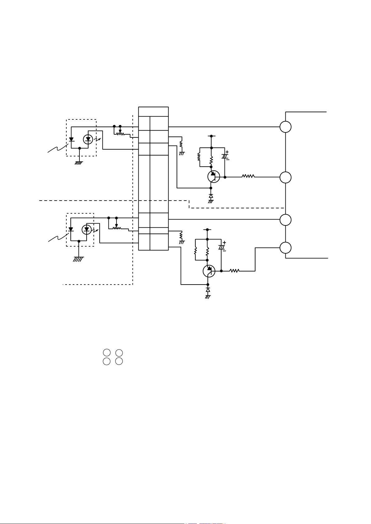
1-2. APC Circuit Operation
It drives the LD to the constant current and adjusts the LD input current , so that the output current is
constant.
IC301 (SSI3721) Pin , : PD IN, Monitor Input of Laser diode APC
IC301 (SSI3721) Pin , : LD OUT, External Current Driver Control output of the LD (Laser Diode)
The detect current from the monitor diode converts to the I/V (Current/Voltage) at the external resistor.
Beforehand, it adjusts a fixed level over for a standard GND.
If this voltage inputs to the PD IN (IC301 Pin 21, 23), it is amplified about 36.4 times (about 31.2dB).
So this voltage outputs from the LD OUT (IC301 Pin 22, 24).
The LD driving element (Q301/Q302) uses the TR more than 200hfe, and controls LD OUT (IC301 Pin 22,
24) connected to the base of Q302/Q301.
The APC control for the each DVD/CD sets Register of the IC301 (SSI3721) according to Disc in the
µ-COM.
DESCRIPTION OF CIRCUIT
1. APC (Automatic Power Control) Circuit
1-1. APC Circuit Constitution
21
23
22
24
Page 9
14
E
A
B
C
F
F
B
A
E
9
10
24
25
26
27
8
5
6
1
11
63
24
26 27
25
7910
CD (A, B, C)
CD (A, B)
DVD (A,B, E, F)
SUM
AMP
DVD RF
CD RF
15
16
7
8
11 12
13 14
3
4
AMP
AMP
MUX
ATT
AGC
AGC
42
GCA
GCA
SUM
AMP
BUFF
MUX
MUX
FE
TE
SIGO
To IC701 3
To IC701 143
To IC701 13
To IC202 119
GCA
41
57
EQ
Phase
Detector
EQ
DVD (A, B)
DVD (E, F)
CD (E, F)
Pick-up Unit
PN301
IC301
SSI3721
2. RF Amplifier Circuit
2-1. RF AMP Constitution
Page 10
15
FOCUS & TRACKING SERVO PROCESS
SLED(Feed) SERVO PROCESS
F
F
B
A
A
E
E
C
Pick - Up
IC301
RF AMP
SSI3721
5
CD
E-F
(A. B. C. E. F)
4
DVD (A. B. E. F)
TE/
DPD TE
SELECTOR
FE
Generating
DPD TE
Generating
TE
FOCUS
ERROR
DETECTOR
FOCUS &
TRACKING
ACTUATOR
IC501
DRIVE
BA5983FP
IC701
CD/DVD SERVO & DSP
CXD3011R-1
F+ F-T+ T-
LEVEL SHIFT
LEVEL SHIFT
FAO
TAO
D/A
DIGITAL
EQUALIZER
(AUTO ADJUSTMENT
CIRCUIT)
SLED
Control
Signal
A/D
TE FE
TE
SAO
SLED MOTOR
Hall Sensor
M
PHO - C
PHO - A
FEED. MOTOR+
FEED. MOTOR-
LEVEL SHIFT
IC501
Q501
DRIVE
BA5983FP
KTD1304
IC502
OP AMP
NJM3414AM
+
IC201
u-COM
SLGNCHG
SLED CLK
B
F-E
B-A
A-B
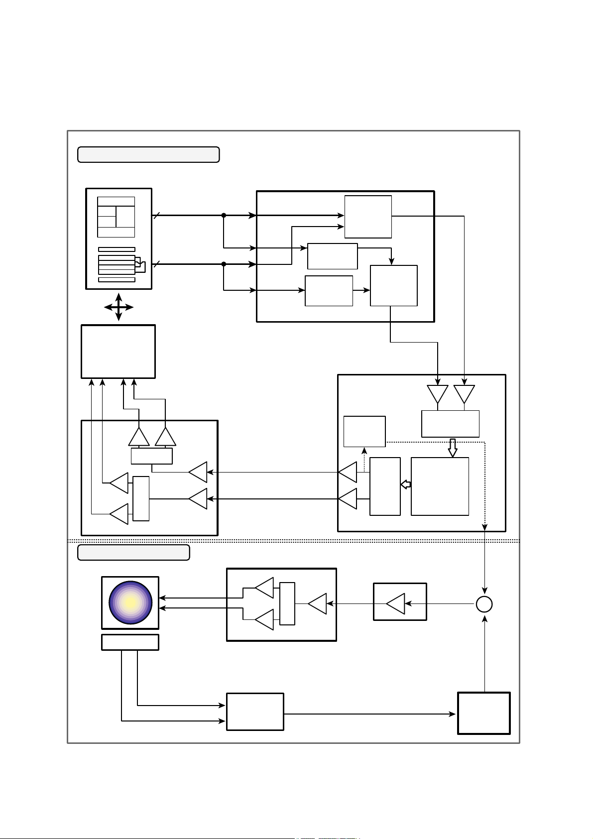
3. Focus/Tracking/Sled Servo Circuit
3-1. FOCUS, TRACKING & SLED SERVO PROCESS
Page 11

16
3-2. Focus Servo for CD/DVD
Focus Servo for CD/DVD is based on focus error signal generated from RF AMP (SSI3721). It standardizes the
laser beam (CD : A, B, DVD : A, B) radiated from the pick-up.
Each other focus gain or path is made at the SSI3721 (IC301) according to the disc, Focus Error signal
output from the FE terminal and input to Servo IC (IC701 CXD3011R-1).
After the first amplification of this signal, the signal is converted to A/D and input to Digital Equalizer Block
assigned the most important part at the Focus Servo, and generates the focus servo with coefficient value
set at the µ-COM through the Digital Filter.
At this Digital Equalizer, auto adjustment for Focus Balance or Focus Loop Gain occurs and the basic offset
value for pick-up is accepted on the balance mode, and set the focus standard level to this value.
After the signal for Focus Servo is converted to the D/A and output through FAO (IC701 CXD3011 ).
This signal drives Focus Actuator through the Focus Drive IC (IC501:BA5983FP).
3-3. Tracking Servo for CD/DVD
For Tracking Servo, CD uses 3 Beam method (E-F), DVD uses DPD (Differential Phase Detect) method
[Phase (F) - Phase (E)]
According to the disc, Tracking Error is set at SSI3721, Gain or Path differs from each other, and the
generated signal output through the TE terminal.
This signal input to TE of IC701, after the first amplification, and converted to A/D.
The signal converted to A/D input to the Digital Equalizer assigned the most important part at the Tracking
Servo, Tracking Servo Gain is generated with Digital Filter coefficient value set according to the disc at the
µ-COM.
* Tracking signal is converted to D/A through the pin TAO terminal of IC701 and input to IC501
(BA5983) tracking drive.
This drive drives the tracking actuator actually.
3-4. Sled Servo (Feed Servo) for CD/DVD
Sled servo operates related with a tracking servo basically
It goes with the progressive track speed according to the disc rotation speed.
Sled drive voltage is generated with a accumulated capacity of tracking error signal and is applied sled
movement voltage according to the track movement capacity, and this voltage outputs to the pin FAO of
IC701. This value is the sled motor drove by the IC501 (Sled drive : BA5983FP). But, the shift speed
for pick-up is not controlled and broke with a only sled servo, itself, in the data access mode, and the
feedback is used according to the sled shift speed at this time. So, the accurated shift speed for
pick-up is controlled added to the sled signal.
The hall sensor is used in the feedback and SLGNCHG (6) output at the µ-COM (IC201) is used with it
in the sled kick or break.
113
112
113
Page 12
17
E
A
B
C
3
4
F
M
PICK-UP
SPINDLE MOTOR
A+B+2C
CD RF
DVD RF
A+B+E+F
IC201
IC701
PLL BLOCK
FG
PLL BLOCK
DVD RF
CD RF
Motor
Hall Sensor
U
HU+
HUHV+
HVHW+
HW-
6
V
W
Speed
Monitoring
u-com
CD/DVD SERVO & DSP
CXD 3011R-1
IC301
RF AMP
SSI3721
IC202
DVD DSP
CXD 1866Q
IC503
OP AMP
NJM2100S
IC401
DRIVE
BA6859A
SPINDLE SERVO PROCESS
LEVEL SHIFT
A, B, 2C
A, B, E, F
SUM
AMP
IC302
AD8012
RF
RF
F
A
E
B
MDP CD
SPDG0
SPDG1
2
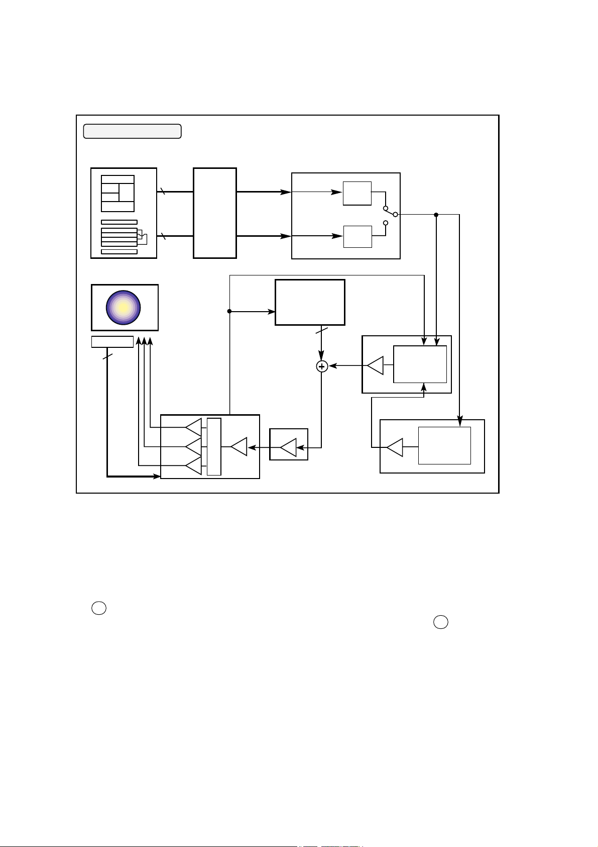
4. Spindle Servo Circuit
4-1. SPINDLE SERVO PROCESS
4-2. Spindle Servo for CD/DVD
DRD-841B consists of the three spindle control respectively.
(1) DVD x 4 : CAV (DVD Single, Dual Layer)
(2) CD x 16 (max.) : CAV (CD-DA, CD-RW, Video-CD, Host command stand-by of CD-ROM and CD-R)
(3) CD x 32 (max.) : CAV (CD-R, CD-ROM play mode)
In the spindle speed control mode respectively.
CD x 16(Max)/CD x 32(Max) CAV drives CAV servo with PLL of RF data read and received MDP CD.
(Pin 117 of IC701)
DVD x 4(Max) CAV drives CAV servo with FG signal and received MDP CD. (Pin 117 of IC701)
Page 13
18
DESCRIPTION OF DATA PROCESSING
1. CD Data Processing Flow
CD
Pickup
Unit
Motor
Drive
Generating
A/B/2C/E/F Signal
H8/3048
Buffer
CD Data Buffering
CXD1866Q
CD-ROM Decoder
and Host Interface
CXD 3011R-1
CD DSP
SSI3721 RF
Signal processing IC
CD TE/FE/SLED
Spindle Control
Command
Data
Status
SDATA
CD DATA
CD RF
MA [0..8]
MDB [0..F]
DATA [0..7]
ADR [0..8]
SICLK
SIXLT
SIDAT
SCLK
CD Data ECC
Receive the order from Host
2'nd ECC
CD Data Buffering
Generating RF Signal
Generating Tracking Error
Generating Focusing Error
CD Servo Control
CD Data Flow Control
Host Command Receive or Data/Status Transfer
Error Correction
Generating Header Sync
Generating Subcode Sync
EFM Demodulation
Page 14
19
2. DVD Data Processing Flow
DVD
Pickup
Unit
Motor
Drive
DVD
TE/FE/Sled/
Spindle control
Sled Control
CXD 3011R-1
CD DSP
H8/3048
Buffer
CXD1866Q
DVD DSP
Command
Data/
Status
DVD RF
DATA [0..7]
ADR [0..8]
MA [0..8]
MDB [0..F]
Generating
A/B/E/F Signal
SSI3721 RF
Signal processing IC
Generating RF Signal
Generating Tracking Error
Generating Focusing Error
Error Signal
Receive the Command from Host
DVD Data Buffering
Copy Protection Control
DVD Data Buffering
DVD Servo Control
DVD Data Flow Control
Host Command Receive or Data/Status transfer
EDC + ECC processing
Generating DVD ID Sync
EFM Demodulation
Page 15
20
CXD 1866Q
HOST DVD
PLAYER
(MPEG2 B/D)
H8/3048
Scrambled MPEG Data
Change the "KEY"
KEY Management Control
3. Copy Protection and Regional Code Management Block
Block Diagram
Brief Process
1. Regional Code for DVD Disc
Ð DVD-ROM drive transfers the regional code of the control data to host by the command of host, the DVD
player of host reads the regional code, and plays title in the case of allowed regional code only.
2. Management of DVD Disc for the scrambled of data
(1) DVD-ROM and DVD player of host generate the ÒKEY 1Ó respectively, transfer to opposite part, the
ÒKEY 2Ó is received, recognizes the data transfer or not with this value, and generates the bus key
encoded the data.
(2) Encoded ÒDisc KeyÓ and ÒTitle KeyÓ host is transfer with the bus Key.
(3) DVD player of host reads the key value, and uses the value to restore the scrambled data.
* Refer to the next page for the details.
Page 16
21
4. About Prevention the DVD-ROM from to be copy
A data is able to encode and record in the disc, if a copyright holder wants to prevent the disc from copying.
In case of a disc enhanced movie of 3 titles......
DISC KEY (2048 Bytes) is used to encode the whole contents in the disc and TITLE
KEY (5 Bytes) is used to encode the title respectively.
So, the data is encoded and stored in a disc through the unknown algorithms
with a disc key and title key. (At this time, the disc key and title key are stored
in a disc.)
ÉAs above, the disc is able to copy when the disc key and title key are
opened.
Then, ROM-DRIVE encodes the disc key and title key and transfers to MPEG2 board.
If you want to play the disc prevented from the copy......
First of all, ROM-DRIVE and MPEG-2 board identify with each other through the procedure as described
below.
1. Drive and host gives and takes the ID of 2bit. This ID is AGID (Authentication Grant ID).
The various decoder boards are attached to the host, in these, AGID sets the MPEG-2 board and drive.
2. After the AGID is set, MPEG-2 board generates the challenge key (10 Byte) and transfers to drive. The
board and drive generate key 1 (5Byte) with the challenge key respectively. (Of course, the Algorithm
generating the key 1 is not known.)
3. Compare with the generated key 1, if it corresponds each other, the first step of authentication is
completed. This is a course to identify the MPEG-2 board with a drive.
4. The second step of authentication is a course to identify a drive with the MPEG-2 board.
The dirve generates a challenge key and transfers it to the MPEG-2 board. The dirve and MPEG-2 board
generate the key 2 (5Byte) with the challenge key, compare with each other, and if it corresponds and the
secondary step of authentication is completed.
5. As above, the identification is completed.
6. The dirve and MPEG-2 board generate the Bus key with the key 1 and key 2 and own it.
7. Dirve encodes the disc key and title key with this Bus key and transfers to the MPEG-2 board.
8. The MPEG-2 board reads the encoded disc key and title key with the Bus key only.
9. MPEG-2 board lets data read from the drive to decode with the read disc key and title key and makes into
the video signal by decoding.
ROM-DRIVE
AGID
HOST
MPEG-2
BOARD
Challenge key
encoded disc key, title key
Page 17

22
5. About the DVD-ROM Regional Code
DISC ROM - DRIVE MPEG-2 BOARD VGA CARD
MONITOR
1
CAN
U.S.A
MIX
CUB
BHS
PRI. VIR
1
BMG
GRL
2
2
ZAF
ISO
SWZ
FIN
POI
FST
LTU
BIR
UKR
TUR
FGY
JRN
TKM
AFG
PAK
CHN
MMR
MNG
RUS
KOR
JPN
HKG
MAC
TWN
PHL
6
3
2
1
5
5
4
1
MDI
MNP
GUM
PLW
PNG
NZL
AUS
4
The disc has
the regional
code of 8 bit.
Example)
The disc
manufactured
in the U.S.A,
has the
number one.
Transfer to
MPEG-2 board
reading the
regional code.
Receiving
data from the
MPEG-2
board and
output
through the
monitor
If the board is setting to the regional
code 1 for the U.S.A. ...
Check the received regional code to
number 1, all or not, transfer the
data to VGA card in accordance with
only a case among the three case.
Regional code
Page 18

23
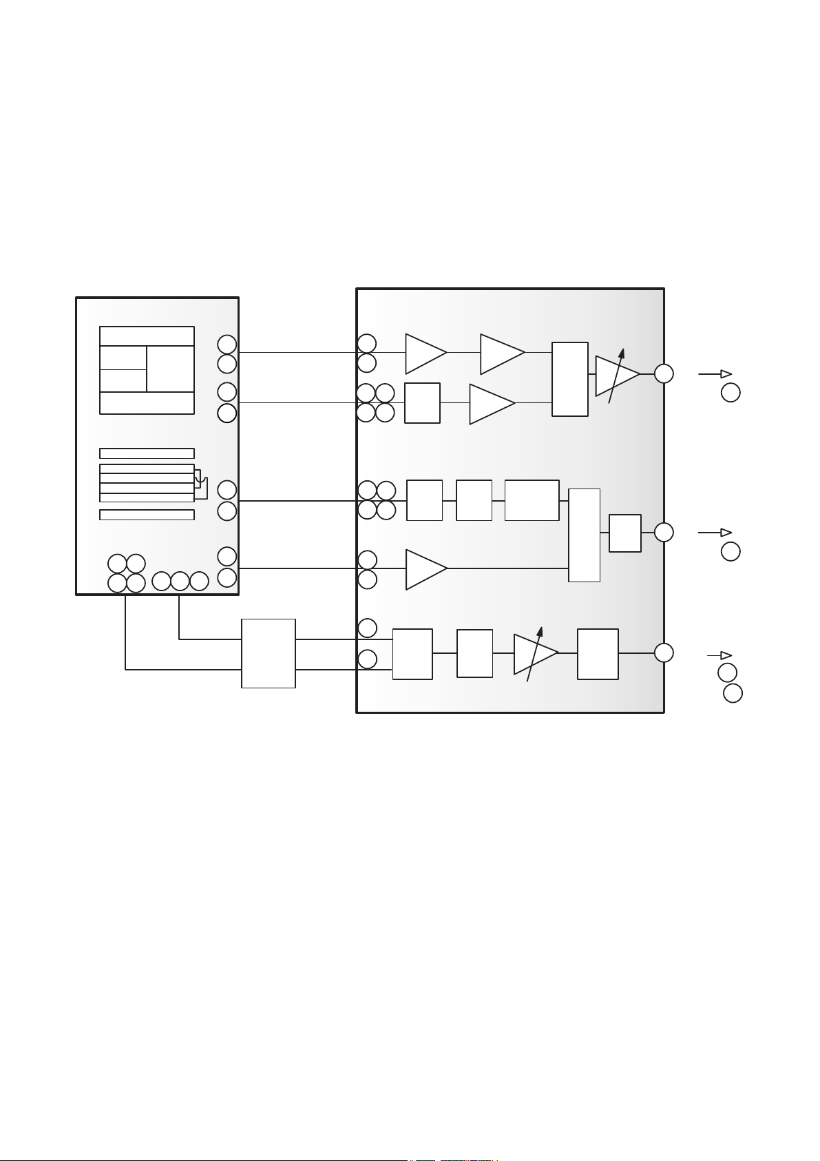
IC301 (SSI3721) : RF Signal Processing for CD/DVD
It amplifies or equalize the RF signal from Pick-up, and generate the TE (Tracking Error) and FE
(Focus Error) signal for Servo respectively.
The TE signal uses the DPD (Differential Phase Detect) method for DVD and 3 Beam method for
CD.
DVD FE = B (A+C) - A (B+D)
CD FE = A(PD1) - B (PD2)
Block Diagram
MAJOR IC INTERNAL BLOCK DIAGRAM AND PIN
DESCRIPTION
1
DVDRFP
2
DVDRFN
MUX
MUX
ATT
AGC
PROGRAMMABLE
EQUALIZER
FILTER
FULL WAVE
OUTPUT INHIBIT
FROM
S-PORT
AGC
CHARGE
PUMP
RECTIFIER
ATTSEL INT
INPUT IMPEDANCE SEL
FROM
S-PORT
DVD
LPF
LPF
LPF
LPF
GCA
GCA
GCA
GCA
EQ
PHASE
DETECTOR
PHASE
DETECTOR
EQ
EQ
EQ
FROM
S-PORT
12dB is added
2
2
VC
3
GCA
GCA
GCA
GCA
12dB is added
high gain mode
SUM
Amp.
A+D
GCA
FROM
S-PORT
MUX
MUX
AGC
Offset
cancel
5
FROM
S-PORT
Focus sel
AGC
FROM
S-PORT
FROM
S-PORT
3
2
4
B+C
FROM
S-PORT
VC
-1
-1
-1
+14dB
TOPHOLD
TOPHOLD
3
+
+
+
+
+
+
+
+
+
+
+
+
+
_
+
_
+
_
+
_
_
+
_
+
_
+
+
+
_
+
4
2
2
62
ATOP
61
ATON
60
AIN
59
AIP
52
FNP
51
FNN
54
DIN
53
DIP
57
SIGO
49
HOLD1
56
BYP
55
RX
42
FE
36
PI
38
TPH
37
DFT
64
CDRFDC
45
HOLD2
44
BYP2
43
CE
9
CP
10
CN
41
TE
27
VCI
26
VC
48
SDEN
47
SDATA
46
SCLK
40
TEI
39
TZC
20
VNB50VNA
28
VPB58VPA
29
MIRR
32
FDCHG
31MB30
MP
33
MLPF2
34
MLPF1
35
MIN
22
DVDLD
24
CDLD
25
LDON
63
CDRF
14
A
13
B
12
C
11
D
3
PD1
4
PD2
19
CE1
18
CEIN
16
E
15
F
17
CDTE
5
A2
6
B2
7
C2
8
D2
21
DVDPD
From serial port
From serial port
Dual APC
INPUT
BUFF
From serial port
Gain select/
Disk Distinguish
From serial port
From serial port
Offset/
Hysteresis
CONTROL
Signals
To each block
SERIAL PORT
REGISTER
VC for internal
VCI for internal
FROM
S-PORT
Offset
cancel
GCA
LPF
Focus sel
FROM
S-PORT
Offset
cancel
4
MUX
MUX
DVD
DPD
RST
FROM
S-PORT
2
4
DPD
Defect ON
VC
TZC
PEAK/BOTTOM
HOLD
LPSEL
From serial port
Input impedance
Select
LD H/L
23
CDPD
IMPUT
BIAS
high gain mode
+14dB
VC
19kohm
high gain mode
+14dB high gain mode
high gain mode
+14dB high gain mode
BuffBuff
BuffBuff
LPF
LPF
BCA DET
COMP
TOPHLD
AGC
CHARGE
PUMP
DAC
TEST
FROM
S-PORT
Focus sel
MUX
SUM
(A2+B2+C2+D2)
Comp.
Page 19

Name
VPA
VPB
VNA
VNB
Description
Power supply pin for the RF block and serial port
Power supply pin for the servo block
Ground pin for the RF block and serial port
Ground pin for the servo block
Pin No.
58
28
50
20
Type
-
-
-
-
POWER SUPPLY PINS
IC301 (SSI3721)
¥ Pin Description
INPUT PINS
24
Name
DVDRFP,DVDRFN
CDRF
AIP, AIN
DIP, DIN
FDCHG*
HOLD1
HOLD2
A,B,C,D
A2,B2,C2,D2
E,F
PD1, PD2
CEIN
TEI
MIN
DVDPD
CDPD
LDON*
Description
RF SIGNAL INPUTS: Differential RF signal attenuator input pins.
RF SIGNAL INPUT: Single-ended RF signal attenuator input pin.
AGC AMPLIFIER INPUTS: Differential AGC amplifier input pins.
ANALOG INPUTS FOR RF SINGLE BUFFER: Differential analog inputs to the
RF single-end output buffer and full wave rectifier.
LOW IMPEDANCE ENABLE: TTL compatible input pin that activates the FDCHG
switches. A low level activates the switches and the falling edge of the internal
FDCHG triggers the fast decay for the MIRR bottom hold circuit. (open high)
HOLD CONTROL: TTL compatible control pin which, when pulled high,
disables the RF AGC charge pump and holds the RF AGC amplifier gain as its
present value. (open high)
HOLD CONTROL: TTL compatible control pin which, when pulled high,
disables the Servo AGC charge pump and holds the Servo AGC amplifier gain
as its present value. (open high)
PHOTO DETECTOR INTERFACE INPUTS: Inputs from the main beam photo
detector matrix outputs.
PHOTO DETECTOR INTERFACE INPUTS: AC coupled inputs for the DPD
from the main beam Photo detector matrix outputs.
CD TRACKING ERROR INPUTS: Inverted(F) and non-inverted(E) inputs of
the OP-Amp for the CD tracking error.
CD PHOTO DETECTOR INTERFACE INPUTS: inputs from the CD photo
detector outputs.
CD CENTER ERROR INPUT: Inverted input of the OP-Amp for the CD center error.
TRACKING ERROR AC COUPLED INPUT: AC couple input for the tracking
zero crossing signal output.
RF SIGNAL INPUT FOR MIRROR: AC coupled inputs for the mirror detection
circuit from pull-in signal output (PI).
APC INPUT: DVD APC input pin from the monitor photo diode.
APC INPUT: CD APC input pin from the monitor photo diode.
APC OUTPUT ON/OFF: APC output control pin. A low level activates LD
output. (open high)
Pin No.
1,2
63
59,60
53,54
32
49
45
14,13,12,11
5,6,7,8
16,15
3,4
18
40
35
21
23
25
Type
I
I
I
I
I
I
I
I
I
I
I
I
I
I
I
I
Page 20

25
Name
ATOP/ATON
FNP, FNN
SIGO
CDRFDC
FE
TE
CE
TZC
DFT
MIRR
PI
DVDLD
CDLD
Description
DIFFERENTIAL ATTENUATOR OUTPUTS: Attenuator outputs.
DIFFERENTIAL NORMAL OUTPUTS: Filter normal outputs.
SINGLE-ENDED NORMAL OUTPUT: Single-ended RF output.
CD RF SIGNAL OUTPUT: Single-ended CD RF summing output.
FOCUSING ERROR SIGNAL OUTPUT: Focus error output reference to VCI.
TRACKING ERROR SIGNAL OUTPUT: Tracking error output reference to
VCI.
CENTER ERROR SIGNAL OUTPUT: Center error output reference to VCI.
TRACKING ZERO CROSSING SIGNAL OUTPUT: Tracking zero crossing
output. Pseudo CMOS output.
DEFECT OUTPUT: Pseudo CMOS output. When defect is detected, the DFT
output goes high. Also the servo AGC output can be monitored at this DFT
pin, when CAR bit7-4 is Ô0011Õ.
MIRROR DETECT OUTPUT: Mirror detect comparator output. Pseudo CMOS
output.
PULL-IN SIGNAL OUTPUT: The summing signal output of A,B,C,D inputs for
mirror detection. Reference to VCI.
APC OUTPUT: DVD APC output pin to control the laser power.
APC OUTPUT: CD APC output pin to control the laser power.
Pin No.
62,61
52,51
57
64
42
41
43
39
37
29
36
22
24
Type
O
O
O
O
O
O
O
O
O
O
O
O
O
OUTPUT PINS
Name
BYP
BYP2
CP
CN
MLPF1
MLPF2
MP
MB
CE1
CDTE
TPH
VC
VCI
RX
Description
The RF AGC integration capacitor C
BYP, is connected between BYP and VPA.
The Servo AGC integration capacitor C
BYP2, is connected between BYP2 and
VNB.
DIFFERENTIAL PHASE TRACKING LPF PIN: The external capacitance is
connected between CN.
DIFFERENTIAL PHASE TRACKING LPF PIN: The external capacitance is
connected between CP.
MIRR SIGNAL LPF PIN: The external capacitance is connected to VPB.
MIRR SIGNAL LPF PIN: The external capacitance is connected to VPB.
MIRR SIGNAL PEAK HOLD PIN: The external capacitance is connected to VPB.
MIRR SIGNAL BOTTOM HOLD PIN: The external capacitance is connected to
VPB.
CENTER ERROR OP AMP OUTPUT: CEIN Opamp output for feedback.
CD TRACKING: E-F Opamp output for feedback.
PI TOP HOLD PIN: An external capacitance is connected to VPB.
REFERENCE VOLTAGE OUTPUT: This pin provides the internal DC bias
reference voltage(+2.5V fix). Output impedance is less than 50
½
.
REFERENCE VOLTAGE INPUT: DC bias voltage input for servo output
reference.
REFERENCE RESISTOR INPUT: An external 12.1 or 8.2 k½, 1% resistor is
connected from this pin to ground to establish a precise PTAT (proportional to absolute
temperature) reference current for the filter.
Pin No.
56
44
9
10
34
33
30
31
19
17
38
26
27
55
Type
-
-
-
-
-
-
-
-
-
-
-
-
-
-
ANALOG PINS
Page 21

26
Name
SDEN
SDATA
SCLK
Description
SERIAL DATA ENABLE: Serial enable CMOS input. A high level input
enables the serial port. (not to be left open)
SERIAL DATA: Serial data bidirectional CMOS pin. NRZ programming data
for the internal registers is applied to this input. (not to be left open)
SERIAL CLOCK: Serial clock CMOS input. The clock applied to this pin is
synchronized with the data applied to SDATA. (not to be left open)
Pin No.
48
47
46
Type
I
I/O
I
SERIAL PORT PINS
Page 22

27
IC201 (H8/3048) : µ-COM
It Controls the total system giving or taking the data from the peripheral ICS.
¥ Pin Description
Pin
No.
1
2
3
4
5
6
7
8
9
10
11
12
13
14
15
16
17
18
19
20
21
22
23
24
25
26
27
28
29
30
31
32
33
34
35
36
37
38
DRD-841B
pin name
VCC1
FDCHG
LDON
HOLD1
HOLD2
SLGNCHG
RFBWCHG
BusyLED
DVDLED
VPP
VSS1
SIDATA
TxD1
SIXLT
RxD1
SICLK
SCLK
TRAYIN
TRAYOUT
SPDG0
SPDG1
VSS2
SVMUTE
AUDMUTE
RFDCSel
VPPON
CGFS
SQSO
SQCK
XRST
XTSEL
DSPMUTE
SENS
DGFS
VCC2
DATA0
DATA1
DATA2
5V
LOW impedance enable to SSI3721
APC output On/Off to SSI3721
Hold Control to SSI3721
Hold Control to SSI3721
Sled drive Gain Change
RF Band width Change Control
Busy LED
DVD LED
Vcc for Flash Memory Version
GND
Serial Data Signal to CXD3011
TxD for flash serial writing
Serial latch signal to CXD3011
RxD for flash serial writing
Serial clock signal to CXD3011
SENS serial clock to CXD3011
Tray close output to BA5983
Tray open output to BA5983
Spindle Gain control signal 0
Spindle Gain control signal 1
GND
Drive IC Mute Control
Audio Mute Control
RFDC Select control signal (ÒLÓ : CD, ÒHÓ : DVD)
'H' when Flash Rom writing
CD GFS signal from CXD3011
Sud Q data from CXD3011
Sud Q serial clock to CXD3011
Reset out to CXD3011, 1866
X' tal Select output to CXD3011
Mute signal to CXD3011
SENS input from CXD3011
DVD GFS from 1866
Data bus to 1866
Data bus to 1866
Data bus to 1866
Data bus to 1866
H8/3048
pin name
Vcc
PB-0
PB-1
PB-2
PB-3
PB-4
PB-5
PB-6
PB-7
Vpp
Vss
P9-0
P9-1
P9-2
P9-3
P9-4
P9-5
P4-0
P4-1
P4-2
P4-3
Vss
P4-4
P4-5
P4-6
P4-7
P3-0
P3-1
P3-2
P3-3
P3-4
P3-5
P3-6
P3-7
Vcc2
P1-0
P1-1
P1-2
D
I
O
O
O
O
O
O
O
O
I
I
I
O
O
I
O
O
O
O
O
O
I
O
O
O
O
I
I
O
O
O
O
I
I
I/O
I/O
I/O
I/O
Description
Page 23

28
Pin
No.
39
40
41
42
43
44
45
46
47
48
49
50
51
52
53
54
55
56
57
58
59
60
61
62
63
64
65
66
67
68
69
70
71
72
73
74
75
76
77
78
79
80
81
DRD-841B
pin name
DATA3
DATA4
DATA5
DATA6
DATA7
VSS3
ADDR0
ADDR1
ADDR2
ADDR3
ADDR4
ADDR5
ADDR6
ADDR7
ADDR8
XRD
XWR
XCS
VSS4
XWAIT
RDE
RDATA
PI
/STBY
/RESET
NMI
VSS5
EXTAL
XTAL
VCC3
RCLK
/TEST MD
FOCGNCHG
RFCTRL
MD0
MD1
MD2
AVCC
VREF
FE
CE
/PLAYKEY
/LOADKEY
Description
Data bus to 1866
Data bus to 1866
Data bus to 1866
Data bus to 1866
Data bus to 1866
GND
Address bus to 1866
Address bus to 1866
Address bus to 1866
Address bus to 1866
Address bus to 1866
Address bus to 1866
Address bus to 1866
Address bus to 1866
Address bus to 1866
Read signal to 1866
Write signal to 1866
Chip select to 1866
GND
Wait signal to 1866
SSI3721 Enable DATA
SSI3721 control DATA
NC
Hardware standby mode transition input
Reset input from reset part
GND
GND
x-tal resonator or external clock input
x-tal resonator input
5V
SSI3721 control clock
TEST MODE
Focus gain change
RF Signal Pass change
Operating mode control 0
Operating mode control 1 ---> Mode 7
Operating mode control 2
5V
Reference voltage for A/D, D/A converters
A/D analog input from SSI3721
Center error input
Play key input
Load key input
H8/3048
pin name
P1-3
P1-4
P1-5
P1-6
P1-7
VSS
P2-0
P2-1
P2-2
P2-3
P2-4
P2-5
P2-6
P2-7
P5-0
P5-1
P5-2
P5-3
Vss
P6-0
P6-1
P6-2
u
/STBY
/RES
NMI
Vss
EXTAL
XTAL
Vcc
P6-3
P6-4
P6-5
P6-6
MD0
MD1
MD2
Avcc
Vref
P7-0
P7-1
P7-2
P7-3
D
I/O
I/O
I/O
I/O
I/O
I
O
O
O
O
O
O
O
O
O
O
O
O
I
O
I
I
I
I
I
I
O
O
I
I
I
I
I
I
I
I
I
Page 24

29
Pin
No.
82
83
84
85
86
87
88
89
90
91
92
93
94
95
96
97
98
99
100
DRD-841B
pin name
/LOADIN
/LOADOUT
APEO
LEADSW
AVSS
XINT0
XINT1
/FOK
SCOR
SLnMA
VSS6
COUT
CD&DVD
SLEDCLK
FG0
FG1
MIRR
BCARF
Fcs DOWN
Description
Tray closed S/W input
Tray opened S/W input
Absolute phase Error
LEAD IN S/W input
GND
INT0 request from 1866
INT1 request from 1866
/FOK from CXD3011
SCOR from CXD3011
IDE jumper input (H:Slave, L:Master)
GND
COUT from CXD3011
DA,DVD spindle signal pass change
Sled motor rotation sense clock input
Spindle motor rotation sensor clock input
Spindle motor rotation sensor clock input
MIRR input from SSI3721
BCARF input from SSI3721
Disc judgement control port
H8/3048
pin name
P7-4
P7-5
P7-6
P7-7
Avss
P8-0
P8-1
P8-2
P8-3
P8-4
Vss
PA-0
PA-1
PA-2
PA-3
PA-4
PA-5
PA-6
PA-7
D
I
I
I
I
I
I
I
I
I
I
I
O
I
I
I
I
I
O
Page 25

30
IC202 (CXD1866R) : LSI processing for DVD-ROM Drive Signal
Block Diagram
39
73
66
70
69
61
79
68
64
65
78
77
169
166
25
8
26
7
11I17
19I21
1
3 I 6
27I29
31I32
34I36
206I208
40
I
41
43
44
45
47
I
50
53
54
56
I
60
72
75
76
168
104
200
199
201
198
171I178
180I187
HOST
I/F
RF
PLL
SYNC
Detect
SYNC
No
Detect
EFM+
Demod
Sector
ID Detect
DMA Controller
(priority resolve & sequencer)
DVD
MAIN DATA
ECC & EDC
DEINTERLEAVE
CD-ROM
Main DATA
ECC & EDC
DESCRAMBLE
Subcode
Deinterleave & ECC
SYNC CONTROL
CD ESP
DAC
I/F
Command
&
Status
Authentication
CPU I/F, DMA Controller
204
205
XWR
XRD
XCS
XINT
XWAT
D [7:0]
A [8:0]
XTL1
XTAL
XTL2
XRST
HCS0
HCS1
XHRD
XHWR
XHAC
DASP
HDB [F:0]
HDRQ
HINT
XS16
REDY
XPDI
XHRS
HA [2:0]
Internal
Clock
Internal
Reset
96
162
119
159
164
GSCOR
GRST
MDAT
BCLK
LRCK
161
DDAT
163
DLRC
158
DBCK
C2PO
WFCK
SCOR
SBIN
EXCK
XRCI
DMA
FIFO
ATAPI
REGISTERs
12bytes
PACKET FIFO
88
81
83
84
85
87
82
CLKOUT
95
DATOUT
93
XLATOUT
94
SCLKOUT
92
SENIN
89
CD-
DSP
I/F
RFIN
XMWR
XCAS
XRAS
XMOE
MA [9:0]
MDB [F:0]
Page 26

31
Pin No. Name I/O Pin Description
1 MDB3 I/O DRAM Data Bus
2 VSS Digital GND
3 MDB4 I/O DRAM Data Bus
4 MDB5 I/O DRAM Data Bus
5 MDB6 I/O DRAM Data Bus
6 MDB7 I/O DRAM Data Bus
7 XMWR O DRAM Write Enable
8 XRAS O ROW Address Strobe
9 VDD 3.3V Digital Power Supply
10 VSS Digital GND
11 MA0 O DRAM Address OUTPUT
12 MA1 O DRAM Address OUTPUT
13 MA2 O DRAM Address OUTPUT
14 MA3 O DRAM Address OUTPUT
15 MA4 O DRAM Address OUTPUT
16 MA5 O DRAM Address OUTPUT
17 MA6 O DRAM Address OUTPUT
18 VSS Digital GND
19 MA7 O DRAM Address OUTPUT
20 MA8 O DRAM Address OUTPUT
21 MA9 O DRAM Address OUTPUT
22 MA10 O DRAM Address OUTPUT
23 MA11 O DRAM Address OUTPUT
24 VDD 3.3V Digital Power Supply
25 XMOE O DRAM Address Enable
26 XCAS O Column Address Strobe
27 MDB8 I/O DRAM Data Bus
28 MDB9 I/O DRAM Data Bus
29 MDBA I/O DRAM Data Bus
30 VSS Digital GND
31 MDBB I/O DRAM Data Bus
32 MDBC I/O DRAM Data Bus
33 VDD5V 5V Analog Power Supply
34 MDBD I/O DRAM Data Bus
35 MDBE I/O DRAM Data Bus
36 MDBF I/O DRAM Data Bus
37 VDD 3.3 Digital Power Supply
38 VSS Digital GND
39 XHRS I Reset Signal from Host
40 HDB7 I/O Host Data Bus
41 HDB8 I/O Host Data Bus
42 VDDS 5V Digital Power Supply
43 HDB6 I/O Host Data Bus
44 HDB9 I/O Host Data Bus
45 HDB5 I/O Host Data Bus
46 VSS Digital GND
47 HDBA I/O Host Data Bus
48 HDB4 I/O Host Data Bus
49 HDBB I/O Host Data Bus
50 HDB3 I/O Host Data Bus
51 VDDS 5V Digital Power Supply
Page 27

32
Pin No. Name I/O Pin Description
52 VDD 3.3V Digital Power Supply
53 HDBC I/O Host Data Bus
54 HDB2 I/O Host Data Bus
55 VSS Digital GND
56 HDBD I/O Host Data Bus
57 HDB1 I/O Host Data Bus
58 HDBE I/O Host Data Bus
59 HDB0 I/O Host Data Bus
60 HDBF I/O Host Data Bus
61 HDRQ O Host DMA Request
62 VDDS 5V Digital Power Supply
63 VSS Digital GND
64 XHWR I HOST Write Signal Input
65 XHRD I HOST Read Signal Input
66 REDY O IO Transfer Ready Output
67 VDD 3.3V Digital Power Supply
68 XHAC I Data Acknowledge Input
69 HINT I/O Interrupt Signal Output
70 XS16 O Data bit wide Select Output
71 VSS Digital GND
72 HA1 I HOST DATA In/Output
73 XPDI I/O HOST Diagnostic In/Output
74 VDDS 5V Digital Power Supply
75 HA0 I HOST DATA In/Output
76 HA2 I HOST DATA In/Output
77 HCS0 I CHIP SELECT 0
78 HCS1 I CHIP SELECT 1
79 DASP I/O Drive Active In/Output
80 VSS Digital GND
81 C2PO I C2 Point Input for CD DSP
82 XRCI I RAM Overflow Input for CD DSP
83 WFCK I Write Frame Clock Input from the CD DSP
84 SCOR I Subcode Oscillating Input from the CD DSP
85 SBIN I Subcode Serial Input from the CD DSP
86 VDDS 5V Digital Power Supply
87 EXCK O Clock Output which read for the Subcode Signal of CD DSP
88 GRST O GRSCOR Reset Output Signal for the CD DSP
89 SENIN I SENS Input Signal for the CD DSP
90 VSS Digital GND
91 VDD 3.3V Digital Power Supply
92 SCLKOUT O SENS Clock Output Signal for the CD DSP
93 DATOUT O CD DSP Serial Command Output Signal
94 XLTOUT O Latch OUT for the CD DSP
95 CLKOUT O Clock Signal for the Transferring DATAOUT for the CD DSP
96 GSCOR I SCOR Input for the CD DSP
97 NC NC
98 NC NC
99 TST0 I Input Signal for testing at the LSI
100 TST1 I Input Signal for testing at the LSI
101 MONITOR O MONITOR OUTPUT
102 VSS Digital GND
103 VDDS 5V Digital Power Supply
Page 28

33
Pin No. Name I/O Pin Description
104 XTAL I 33.86688MHz CLOCK INPUT
105 VSS Digital GND
106 MONITOR O MONITOR OUTPUT
107 LINK O LINK Signal Monitor OUTPUT
108 PLCK O PLL CLOCK OUTPUT
109 VDD5V 5V Analog Power Supply
110 VDD 3.3V Digital Power Supply
111 RFTTLIN I RF TTL INPUT
112 DASYO O Data Output to Asymmetry Compensation Circuitry
113 GNDA Analog GND
114 ASF1 I Asymmetry Compensation Filter
115 ASF2 I Asymmetry Compensation Filter
116 DASYI I Data Input of Asymmetry Compensation Circuitry
117 AMPOUT O Amplifier Output of Asymmetry Compensation Circuitry
118 RFDCC I RF DC Cut Control
119 RFIN I RF Signal Input
120 DLR2 I Terminal for the Read Channel Test
121 DLR1 I Terminal for the Read Channel Test
122 DLYI I Terminal for the Read Channel Test
123 VCCA 3.3V Analog Power Supply
124 VCCA 3.3V Analog Power Supply
125 VCOR2 O Connecting Terminal which Selecting for the VCO Voltage
126 VCOR1 O Connecting Terminal which Selecting for the VCO Voltage
127 VCOIN I VCO INPUT
128 GNDA Analog GND
129 GNDA Analog GND
130 LPFDC I PLL LPF DC Input
131 LPF5 O PLL LPF 5
132 LPF4 I PLL LPF 4
133 VC1 I Central Voltage Input for the RF PLL
134 LPF3 O PLL LPF 3
135 LPF2 O PLL LPF 2
136 LPF1 I PLL LPF 1
137 VCCA 3.3V Analog Power Supply
138 VCCA 3.3V Analog Power Supply
139 FDO O Frequency Detector Output
140 PDO O Phase Detector Output
141 PDHVCC I Central Voltage Input for the RF PLL
142 GNDA Analog GND
143 GNDA Analog GND
144 SPO O Spindle Control Output
145 VC2 I Central Voltage Input for the RF PLL
146 MDIN2 I MDP Input
147 MDIN1 I MDP Input
148 VCCA 3.3V Analog Power Supply
149 CLVS O CLVS Control Output
150 MDSOUT O Frequency Differential Output for the Enhanced CLV Circuit
151 MDPOUT O Phase Differential Output for the Enhanced CLV Circuit
152 APEO O Absolute Phase Error
153 VSS Digital GND
154 GFS O Interface Select Input
155 VCOIN-E I Clock Signal for the VCO Testing
Page 29

34
Pin No. Name I/O Pin Description
156 VDD 3.3V Digital Power Supply
157 VSS Digital GND
158 DBCK O DAC Bit CLOCK
159 BCLK I Bit CLOCK Input Signal for the CD DSP
160 VDD 3.3V Digital Power Supply
161 DDAT O PCM Data Output for the DAC
162 MDAT I Serial Data Input Signal for the CD DSP
163 DLRC O LR CLOCK Output Signal for the DAC
164 LRCK I LR CLOCK Input Signal for the CD DSP
165 VDD5V 5V Analog Power Supply
166 XTL2 O X-TAL Output Signal
167 VSS Digital GND
168 XTL1 I X-TAL Input Signal
169 XRST I CHIP RESET Input Signal
170 VDD 3.3V Digital Power Supply
171 D0 I/O 8Bit DATA BUS
172 D1 I/O 8Bit DATA BUS
173 D2 I/O 8Bit DATA BUS
174 D3 I/O 8Bit DATA BUS
175 D4 I/O 8Bit DATA BUS
176 D5 I/O 8Bit DATA BUS
177 D6 I/O 8Bit DATA BUS
178 D7 I/O 8Bit DATA BUS
179 VSS Digital GND
180 A0 I Micom Data In/Output
181 A1 I Micom Data In/Output
182 A2 I Micom Data In/Output
183 A3 I Micom Data In/Output
184 A4 I Micom Data In/Output
185 VDD 3.3V Digital Power Supply
186 A5 I Micom Data In/Output
187 A6 I Micom Data In/Output
188 A7 I Micom Data In/Output
189 A8 I Micom Data In/Output
190 VSS Digital GND
191 A9 I Micom Data In/Output
192 A10 I Micom Data In/Output
193 A11 I Micom Data In/Output
194 A12 I Micom Data In/Output
195 A13 I Micom Data In/Output
196 A14 I Micom Data In/Output
197 VDD5V 5V Analog Power Supply
198 XWAIT O Wait Signal which the Micom Accesses the Buffer Memory
199 XRD I Strobe Signal which read for the Resistor Status
200 XWR I Strobe Signal which write for the Resistor Status
201 XCS I Chip Select Signal
202 VSS Digital GND
203 VDD 3.3V Digital Power Supply
204 XINT0 O Micom Interrupt
205 XINT1 O Micom Interrupt
206 MDB0 I/O DRAM Data Bus
207 MDB1 I/O DRAM Data Bus
208 MDB2 I/O DRAM Data Bus
Page 30

35
IC401 (BA6859AFP) : Spindle Motor Drive IC
It drives the spindle motor receiving the spindle control signal at IC701 (CXD3011R-1) in CD & DVD
mode.
2
4
7
8
9
10
28
27
25
24
23
22
21
20
18
17
16
15
11
12
13
14
TL
TSD
GAIN
CONTROL
Hall 1
Hall 2
Hall 3
Hall Bias
BRAKE MODE
HALL AMP
SHORT BRAKE
P S
A3
A2
A1
H1+
H1-
H2 +
H2 -
H3 +
H3 -
FIN
GND
RNF
R
NF
VM
VCC
FG
VM
PS
EC
ECR
FR
SB
CNF
BR
VH
+
-
+
-
+
-
+
+
-
-
+
-
+
-
TORQUE
SENSE AMP
SERVO
SIGNAL
CURRENT
SENSE AMP
VCC
Vcc
VCC
D
CK
Q
Q
R
DRIVER
Pin No.
1
2
3
4
5
6
7
8
9
10
11
12
13
14
15
16
17
18
19
20
21
22
23
24
25
26
27
28
FIN
Description
N.C.
Output3 for motor
N.C.
Output2 for motor
N.C.
N.C.
Output1 for motor
GND
Hall input Amp1. positive input
Hall input Amp1. negative input
Hall input Amp2. positive input
Hall input Amp2. negative input
Hall input Amp3. positive input
Hall input Amp3. negative input
Hall Bias
Change for BRAKE MODE
Capacitor connection pin for phase compensation
Short brake terminal
N.C.
Rotation detect terminal
Torque control standard voltage input terminal
Torque control voltage input terminal
START/STOP Switching
FG signal output terminal
5V Power supply for signal division
N.C
Power supply for driver
Power supply for driver division
GND
Pin Name
N.C.
A
3
N.C.
A
2
N.C.
N.C.
A
1
GND
H
1
+
H
1
-
H
2
+
H
2
-
H
3
+
H
3
-
V
H
BR
C
NF
SB
N.C.
FR
E
CR
E
C
PS
FG
Vcc1
N.C
V
M1
R
NF
FIN
Block Diagram
¥ Pin Description
Page 31

36
IC501 (BA5983 FP)
1) It controls the sled movement and takes the tray to open/close in track search mode.
2) It controls the Focus/Tracking Actuator receiving the focus error or tracking error signal from IC701.
+
-
+
-
+
-
+
-
115
16
17
18
19
20
21
22
23
24
25
26
27
28
2
3
4
5
6
7
Pin No. Pin No.
BIAS IN Bias amplifier input
Driver CH1 positive input
Driver CH1 negative input
Driver CH2 negative input
Driver CH2 negative output
CH3 negative input
CH4 negative input
CH4 positive input
Driver CH2 positive input
Driver CH2 positive output
CH3 positive input
CH4 output
Driver CH1 negative output
Driver CH4 negative output
Driver CH1 positive output
Driver CH4 positive output
Driver CH3 negative output
Driver CH3 positive output
Driver CH1 output
Driver CH2 output
OPIN1(+)
OPIN2(+)
OPIN3(+)
OPIN1(-)
OPIN2(-)
OPIN3(-)
OPIN4(+)
PreVcc PreVcc
OPIN4(-)
OPOUT 1
OPOUT 2
CH3 output
OPOUT 3
OPOUT 4
8
9
10
11
12
13
14
GND GND
CH1~3 standby control
STBY1
PowVcc1 PowVcc (CH1,2)
PowVcc2
STBY2
GND GND
PowVcc (CH3,4)
CH4 standby control
VO2 (-)
VO1 (-)
VO4 (-)
VO2 (+)
VO1(+)
VO4(+)
VO3 (-)
VO3(+)
Pin name
Description Pin name Description
1 2 3 4 5 6 7 8 9 1011121314
-
-
+
-
-
+
-
+
+
-
+
+
-
+
-
+
-
+
-
+
-
+
-
+
10K10K10K
10K
10K
10K
10K 10K
10K 10K
10K
10K 10K
10K
10K
10K
10K
20K
10K
20K
10K
10K
10K
CH1CH2
CH3 CH4
Vcc
Vcc
Vcc
CH1, 2, 3
CH4
28 27 26 25 24 23 22 21 20 19 18 17 16 15
Standby
Standby
LEVEL
SHIFT
LEVEL
SHIFT
LEVEL
SHIFT
LEVEL
SHIFT
¥ Pin Description
Page 32

37
IC701 (CXD3011R - 1) : DSP
Generates Error Signal and return to the Servo by the Signal from RF Amplifier IC.
52
83 84 5 6 51
136
135
57
58
59
7
134
122
107
129
123
124
141
132
131
13
15
16
24
64
65
67
66
69
68
117
118
116
133
71
140
142
143
22 43 60 94
130
17
137
93 81 82 23 50 77
101
105
102
100
103
104
121
12
139
86 78 85
110 114
111
95
99
98
62
63
25
79
80
88
87
29
61
112
113
115
4
3
2
10
11
9
8
Clock
Generator
32K RAM
Digital PLL
Vari-Pitch
double
speed
EFM
Demodulator
Sync
D/A
protector
Address
generator
8Fs Digital Filter
+
1 bit DAC
Priority
encoder
Timing
CLV
Servo
auto
CAV
Digital Out
Generator1
Timing
Generator2
Noise
Shaper
18~times
oversampling
filter
P~W
Subcode
Subcode Q
processor
processor
processor
processor
CPU
interface
Servo
Interface
SERVO DSP
DAC O
p
Amp
FOCUS SERVO
TRACKINGSERVO
FOCUS
SLED
TRACKING
SLED SERVO
O
p
Amp
AnaSw
A/D
CONVERTER
MIRR
DFCT
FOK
Peak
detector
Error
corrector
data
processor
Serial/parallel
processor
Register
XTLO
DV
DD
1
DV
DD
2
DV
DD
3
DV
DD
4
DV
DD
5
DV
SS
1
DV
SS
2
DV
SS
3
DV
SS
4
DV
SS
5
AV
SS
1
AV
SS
2
AV
SS
3
AV
SS
4
AV
SS
5
AV
SS
6
BSSD
AV
DD
1
AV
DD
2
AV
DD
3
AV
DD
4
AV
DD
5
AV
DD
6
XTLI
VPCO1
VPCO2
XTSL
PCMDI
BCKI
LRCKI
DTSO
XWO
RMUTO
LMUTO
Error Rate
Counter
sequencer
Selector
OSC
MCKO
V16M
VCKI
FSTIO
C4M
C16M
VCTL
PDO
PCO
VCOI
FILI
FILO
CLTV
RFAC
ASYI
ASYO
ASYE
WFCK
SCOR
EXCK
SBSO
SQCK
SQSO
MDP
MDS
MON
FSW
PWMI
TEST
TES2
TES3
XRST
ADIO
RFDC
CE
TE
SE
FE
VC
SAO
TAO
FAO
COUT
SENS
DATA
DOUT
MUTE
PSSL
PWMLP
PWMLN
PWMRP
PWMRN
DA16(48PCM)
DA15(48BCK)
DA14(64PCM)
DA13(64BCK)
DA12(64LRCK)
DA11
~DA01
MD2
CLOK
XLAT
MIRR
DFCT
FOK
VCOO
SIGNAL PROCESSOR BLOCK
SERVO BLOCK
DAC BLOCK
35
38~42,
44~49
34
33
31
30 32 28 74 75 76
8
MUX
*
* : Asymmetry
Correction
Block Diagram
Page 33

38
IC701 CXD3011R - 1
¥ Pin Description
Pin No. Symbol I/O Description
2 SE I Slide Error input
3 FE I Focus Error input
4 VC I Center voltage input
5 VPCO1 O 1, Z, 0 Output of VCO2 charge pump for vari-pitch EFM PLL
6 VPCO2 O 1, Z, 0 Output 2 of VCO2 charge pump for vari-pitch EFM PLL
ON/OFF switching by Command S E
7 VCTL I Input of VCO2 control voltage for vari-pitch EFM PLL
8 FILO O Analog Output of Filter for master PLL (slave = digital PLL)
9 FILI I Input of filter for master PLL
10 PCO O 1, Z, 0 Output of charge pump for master PLL
11 CLTV I VCO control voltage lnput
12 A V
SS1 Analog GND
13 RFAC I EFM signal input
14 BIAS I Asymmetry circuit constant current input
15 ASYI I Asymmetry comparator circuit voltage input
16 ASYO O 1, 0 EFM full-swing output (L=V
SS, H=VDD)
17 A V
DD1 Analog power supply
22 D V
DD1 Digital power supply
23 D V
SS1 Digital GND
24 ASYE I Asymmetry circuit ON/OFF (L=OFF, H=ON)
25 PSSL I Input used to switch the audio data output mode. (L=serial, H=parallel)
26 WDCK O 1, 0 D/A interface for 48-bit slot. Word clock f=2Fs
27 LRCK O 1, 0 D/A interface for 48-bit slot. LR clock f=Fs
28 LRCKI I LR clock input to DAC (48-bit slot)
29 DA16 O 1, 0 Outputs DA16 (MSB) when PSSL=1, or serial data output from the 48-bit slot (2's
complements, MSB first) when PSSL=0.
30 PCMDI I Audio data input to DAC (48-bit slot)
31 DA15 O 1, 0 Outputs DA15 when PSSL=1, or bit clock output from the 48-bit slot when PSSL=0.
32 BCKI I Bit clock input to DAC (48-bit slot)
33 DA14 O 1, 0 Outputs DA14 when PSSL=1, or serial data output from the 64-bit slot (2's
complements, LSB first) when PSSL=0.
34 DA13 O 1, 0 Outputs DA13 when PSSL=1, or bit clock output from the 64-bit slot when PSSL=0.
35 DA12 O 1, 0 Outputs DA12 when PSSL=1, or LR clock output from the 64-bit slot when PSSL=0.
38 DA11 O 1, 0 Outputs DA11 when PSSL=1, or GTOP when PSSL=0.
39 DA10 O 1, 0 Outputs DA10 when PSSL=1, or XUGF when PSSL=0.
40 DA09 O 1, 0 Outputs DA9 when PSSL=1, or XPLCK when PSSL=0.
Page 34

39
Pin No. Symbol I/O Description
41 DA08 O 1, 0 Outputs DA8 when PSSL=1, or GFS when PSSL=0.
42 DA07 O 1, 0 Outputs DA7 when PSSL=1, or RFCK when PSSL=0.
43 DV
DD2 Digital Power supply
44 DA06 O 1, 0 Outputs DA6 when PSSL=1, or C2PO when PSSL=0.
45 DA05 O 1, 0 Outputs DA5 when PSSL=1, or XRAOF when PSSL=0.
46 DA04 O 1, 0 Outputs DA4 when PSSL=1, or MNT3 when PSSL=0.
47 DA03 O 1, 0 Outputs DA3 when PSSL=1, or MNT2 when PSSL=0.
48 DA02 O 1, 0 Outputs DA2 when PSSL=1, or MNT1 when PSSL=0.
49 DA01 O 1, 0 Outputs DA1 when PSSL=1, or MNT0 when PSSL=0.
50 DV
SS2 Digital GND
51 XTSL I X'tal selection input
52 MCKO O 1, 0 Clock output. Inverse output of XTLI
57 FSTIO I/O 1, 0 Clock input/output for Digital servo
(2/3 frequency demultiplication input of XTLI)
58 C4M O 1, 0 1/4 frequency demultiplication output of XTLI. Affected by vari-pitch
59 C16M O 1, 0 16.9344MHz output. Subject to vari-pitch control.
60 DV
DD3 Digital power supply
61 MD2 I Digital-Out ON/OFF control. "H" for ON, "L" for OFF.
62 DOUT O 1, 0 Digital-Out output.
63 MUTE I "H" for muting, "L" for release.
64 WFCK O 1, 0 WFCK (Write Frame Clock) output
65 SCOR O 1, 0 "H" when subcode Sync S0 or S1 is detected.
66 SBSO O 1, 0 Serial output of Sub P to W
67 EXCK I Clock input for reading SBSO
68 SQSO O 1, 0 Outputs 80-bit Sub Q and 16-bit PCM peak-level data.
69 SQCK I Clock input for reading SQSO
70 SCSY I Input of GRSCOR
71 XRST I System reset. "L" for resetting
74 XWO I Window open input for DAC synchronization. Generally, at "L" window open
75 RMUTO O 1, 0 Audio DAC, zero detecting block for R channel
76 LMUTO O 1, 0 Audio DAC, zero detecting block for L channel
77 DV
SS3 Digital GND
78 AV
SS4 Analog GND
79 PWMRN O 1, Z, 0 PWM output for Audio DAC, R channel, Reverse phase
80 PWMRP O 1, Z, 0 PWM output for Audio DAC, R channel
Page 35

40
Pin No. Symbol I/O Description
81 AVDD4 Analog power supply
82 AV
DD5 Power supply for master clock
83 XTLO O 1, 0 X'tal oscillation circuit output of master clock.
84 XTLI I X'tal oscillation circuit input of master clock.
85 AV
SS5 GND for master clock
86 AV
SS3 Analog GND
87 PWMLP O 1, Z, 0 PWM output for Audio DAC, L channel
88 PWMLN O 1, Z, 0 PWM output for Audio DAC, L channel, Reverse phase
93 AV
DD3 Analog power supply
94 DV
DD4 Digital power supply
95 SENS O 1, Z,0 SENS output to CPU
96 SCLK I Clock for SENS serial data
97 ATSK I Pin for Anti-shock
98 DATA I Serial Data input from CPU
99 XLAT I Latch input from CPU
100 CLOK I Serial Data transfer clock input from CPU
101 DV
SS4 Digital GND
102 COUT I/O 1, 0 Track number count signal input/output
103 MIRR I/O 1, 0 Mirror signal input/output
104 DFCT I/O 1, 0 Defect signal input/output
105 FOK I/O 1, 0 Focus OK input/output
106 TESO O Test pin
107 FSW O 1, Z,0 SCOR of command S 8, GRSCOR output when SEL="H"
110 AV
SS6 Analog GND
111 SAO O DAC analog output of Sled filter
112 TAO O DAC analog output of Tracking filter
113 FAO O DAC analog output of Focus filter
114 BSSD I Constant current input for DAC analog of servo filter
115 AV
DD6 Analog power supply
116 MON O 1, 0 Output for spindle motor ON/OFF control
117 MDP O 1, Z, 0 Output for spindle motor servo control
118 MDS O 1, Z, 0 Output for spindle motor servo control
119 LOCK I/O 1, 0 Output is "H" when the GFS signal sampled at 460Hz is "H". Output is "L" when the
GFS signal is "L" 8 or more times is succession.
120 SSTP I Disc inner periphery detection signal input
121 DV
SS5 Digital GND
122 DTS0 I Test pin. Normally "L"
Page 36

41
* The below pin numbers are no connection pin 1, 18~21, 36, 37, 53~56, 72, 73, 89~92, 108, 109, 125~128, 144.
Notes :
¥ The data at the 64-bit slot is output in 2's complements on an LSB-first basis. The data at the 48-bit slot is
output in 2's complements on an MSB-first basis.
¥ GTOP monitors the state of Frame Sync protection. ("H" : Sync protection window released)
¥ XUGF is a negative Frame Sync pulse obtained from the EFM signal before Frame Sync protection is
effected.
¥ XPLCK is an inversion of the EFM PLL clock. The PLL is designed so that the falling edge of XPLCK
coincides with a change point of the EFM signal.
¥ The GFS signal turns "H" upon coincidence between Frame Sync and the timing of interpolation protection.
¥ RFCK is a signal generated at 136-µs periods using a crystal oscillator.
¥ C2PO is a signal to indicate data error.
¥ XRAOF is a signal issued when a jitter margin of +28F is exceeded by the 32K RAM.
Pin No. Symbol I/O Description
123 TES2 I Test Pin. Normally "L"
124 TES3 I Test Pin. Normally "L"
129 PWMI I External input of spindle motor
130 DV
DD5 I Digital power supply
131 VCOO O 1, 0 Output of oscillation circuit analog EFM PLL
132 VCOI I Input to oscillation circuit for analog EFM PLL. f
LOCK=8.6436MHz
133 TEST I Test Pin. Normally "L"
134 PDO O 1, Z, 0 Output of charge pump for analog EFM PLL
135 VCKI I Clock input from external VCO for vari-pitch control. fc
center=16.9344MHz
136 V16M O 1, Z, 0 Output of VC02 oscillation for vari-pitch EFM PLL
137 AV
DD2 Analog power supply
138 IGEN I Resistor connection pin of current source reference for OP Amp
139 AV
SS2 Analog GND
140 ADIO O OP Amp output
141 RFDC I RF signal input
142 CE I Center servo analog input
143 TE I Tracking error signal input
Page 37

42
TROUBLESHOOTING GUIDE
Reset or Power ON.
¥ Check the power short.
¥ Check PC power cable, power
supply and fuse.
Repair PC power supply.
NO
Replace IC103 (3.9V Regulator).
NO
YES
OK
YES
Are the pin 44
and 41 of PN 201 +5V and +12V
respectively after the power
cable connecting?
Is the pin 4 of
IC103 3.9V?
Replace IC102 (3.3V Regulator).
NO
YES
Is the pin 4 of
IC102 3.3V?
Replace X201, X202 and X701
when the power supply of IC201,
IC202 and IC701 is OK.
NO
YES
Do the X201, X202
and X701 oscillating?
Replace IC201 when the IC101
(RESET IC) is non-ok.
NO
YES
Does the pin 63
of IC201 change 0V to 5V at
the power supply initial
input mode?
Refer to ÒTray open / close
doesnÕt work.Ó
NO
YES
Does the tray open or
close?
(Check it after connecting the power cable only no interface cable)
A
Page 38

43
Refer to ÒLaser Diode is not on.Ó
A
NO
Refer to ÒServo part is
abnormalÓ.
NO
YES
Is the Laser Diode
ÒONÓ?
Does the Focus move
up and down?
Refer to ÒDisc Reading
operation is abnormal.Ó
NO
YES
Is the TOC area
on the disc read? (Does
the LED flicker?)
Page 39

44
Check and replace the
SW602 or peripheral resistor
and pattern short.
Tray open/close doesnÕt work.
NO
YES
Does the
waveform appear at
the IC201 pin 81 when push
the SW802 (open/close)?
B
5V
Push period
Check and replace the R509,
R510, R511 or pattern short.
NO
Does the
waveform appear
at the R524 connected to
IC501 pin 26, that is connected
to IC501 reversely?
3.7V
2V
0V
0.2V
close
normal
open
Does the
signal appear
at the IC501 pin 15
and 16?
6V
6V
closing
period
Pin 15
Pin 16
opening
period
YES
Check and replace the IC201.
NO
Does the
IC201 pin 18 and
19 appear in the tray
open/close mode
as below
ƒT?
YES
YES
Check the cold soldering for
the IC501 and then replace
IC501.
NO
ƒT: TRAY IN TRAY OUT
(18) (19)
OPEN 0.2VÐ>2V 0.2VÐ>2V
CLOSE 5VÐ>2V 3VÐ>2V
STOP 2V 2V
Page 40

45
B
Is the
connecting status normal
between the PN502
and loading motor?
Check the cold soldering for
the PN502 and wire
connecting status and then
replace loading motor.
NO
YES
Open/close mode is normal.
Page 41

46
Refer to ÒReset or Power ONÓ.
Laser Diode is not ON.
YES
Check the cold soldering for
the IC301 and then replace
IC301.
Check the cold soldering for
the IC201 and then replace
IC201.
Check the cold soldering for
the transistor Q302 and then
replace Q302.
Replace the Pick-up.
YES
YES
NO
NO
NO
NO
CD PART
DVD PART
NO
Does the focusing
actuator move up and
down?
Is the PN301
pin 22 about 2V at the
initial power on mode?
Does the
signal appear at IC301
Pin 22?
Is the collector of
transistor Q302 about
2V?
YES
YES
Does the
signal appear at IC301
Pin 25?
C
3V
5V
0V
5V
OK
Page 42

47
C
Is the PN301
pin 5 about 2V
at the initial power on mode?
NO
NO
NO
YES
YES
Replace the Pick-up.
Check the cold soldering for
the transistor Q301 and then
replace Q301.
Does the
signal appear at IC301
Pin 24?
Is the collector of
transistor Q301 about
2V?
3V
5V
Check the cold soldering for
the IC301 and then replace
IC301.
Check the cold soldering for
the IC201 and then replace
IC201.
NO
YES
Does the
signal appear at IC301
Pin 25?
0V
5V
YES
OK
Page 43

48
¥ Check the cold soldering for
the IC302 pin 5, 6, 7.
¥ Check the FPC connecting
status PN 301.
¥ Check the pick up.
Check the CD RF SIGNAL.
NO
YES
Does the RF out signal
output from pick-up?
(IC301 pin 63 : CD RF)
¥ Check the cold soldering for
the C347, C302, C303, C304,
C305 and C307.
¥ Replace IC301.
NO
YES
Does the RF
signal output at the
IC301 Pin 57?
(RF Level : about 1.5V)
Check the cold soldering for the
C737, C732 and Q701.
NO
Does the
RF signal input to the
IC701 Pin 13?
Page 44

49
¥ Check the cold soldering for
the IC302 pin 1, 2, 3.
¥ Check the FPC connecting
status PN301.
¥ Check the pick up.
Check the DVD RF signal.
NO
YES
Does the RF out signal
output from the pick-up?
(IC301 pin 1 : DVD RF)
¥
Check the cold soldering for the
C348, C302, C303, C304, C305
and C307.
¥ Replace IC301.
NO
YES
Does the RF signal output
from the IC301 pin57?
(RF Level : about 1.5V)
Check the cold soldering for the
C746, R754 and IC702.
NO
YES
Does the RF signal
output from the IC702
pin4?
Check the cold soldering for the
R747, R748, R749, R738, R739,
C119 and C742.
NO
Does the RF signal
input to the IC202
pin119?
Page 45

50
Check the cold soldering for the
IC701 and then replace IC701.
Disc Rotation is unstable.
NO
YES
Does the spindle
motor kick signal and
driving signal output from
the IC701 pin117?
<Fig.1>
<Fig. 1>
Check the cold soldering for the
R421, C409 and IC402 and then
replace IC402.
NO
YES
Does the
spindle driving signal
output from IC402 normally?
(CD: IC402 pin7 <Fig.2>
DVD:IC402 pin6
<Fig.3>)
<Fig. 2>
Check the cold soldering for the
R415, R408, R422, C415 and
IC503 and then replace IC503.
NO
YES
Does the
spindle driving signal
output from IC503 pin1
normally? <Fig. 4>
(For CD and DVD)
<Fig. 4>
Check the cold soldering for the
IC401 and then replace IC401.
Replace the Spindle motor.
NO
YES
YES
Does the
spindle driving signal
output from IC401 pin 2, 4
and 7 normally?
(For CD and DVD)
<Fig.5>
Check the cold soldering
for the PN401 and FPC
connecting status.
<Fig. 5>
<Fig. 3>
Page 46

51
Servo part is abnormal.
Insert a disc.
Refer to ÒSpindle motor
Rotation is failedÓ.
¥ Check the FPC connecting
status PN501.
¥ Check the cold soldering for
the pin 17, 18 of IC501.
Refer to ÒLaser Diode is not
ONÓ.
YES
YES
YES
YES
YES
YES
YES
YES
NO
NO
Check the cold soldering for the
IC701 and IC202.
A
B
NO
NO
NO
NO
NO
C
CD: CGFS
IC701 Pin 41
DVD: DGFS
IC202 Pin 154
Does the pick-up slide
inner track?
Does the disc rotate?
Is the Laser Diode on?
Does the focus move up
and down?
Is the FOK signal ÒHÓ?
(IC701 Pin 105)
Does the disc rotate in
high speed repeatedly?
Is the GFS signal ÒHÓ?
OK
Page 47

52
Check the cold soldering for
the IC501(BA5983FP)
pin 13, 14.
Replace IC501.
Check the FG1 signal line.
Check the cold soldering for
the IC401.
YES
NO
YES
A
B
NO
Check the circuit between the
IC501 Pin 3, 4
and the IC701 Pin 113.
C
Check the FAO signal.
(IC701 Pin 113 )
Does the square wave
output at the IC401 Pin 24
(FG1)?
V
1.95V
T
Check the cold soldering
for the IC301 Pin 1, 42, 63 and
C347, C348 and IC701 Pin 3, 141.
Page 48

53
Check the spindle drive
signal.
(IC401 BA6859 Pin 22)
Check the cold soldering for
the IC401(BA6859).
Replace the IC401(BA6859).
Check the cold soldering for
the IC402(TC4W53).
Spindle Motor Rotation is
failed.
Check the MDP signal.
(IC701 CXD3011 Pin 117)
Check the cold soldering
for the IC701(CXD3011).
Check the X-tal oscillating
(33.8688MHz) at the
IC701(CXD3011) Pin 83 and 84.
Check the IC701(CXD3011)
Pin 98, 99 and 100 (µ-com
I/F line).
Check the cold soldering
for the IC201(H8/3048)
µ-com.
Check the cold soldering
for the IC401 (BA6859).
NO
YES
YES
YES
NO
Does the above
signal output after the
tray close?
Does the above
signal output after the
tray close?
Is the disc rotation OK?
V
1.95V
100ms
NO
T
Page 49

54
Check the cold soldering for the
IC201.
Check the cold soldering for
the SW801, R847 and R844.
Non working Audio play
key.
YES
YES
NO
NO
Is IC201 pin 80 5V
before pressing the
SW801?
Is IC201 pin 80 0V
pressing the SW801?
Check the cold soldering
for the X701 (33.86MHz).
Page 50

55
No Audio output.
Check the headphone jack and
cable.
Insert the audio disc.
Check the IC201 Pin 24.
YES
Check the MICOM IC201 pin 24.
NO
NO
YES
NO
NO
Replace IC801.
YES
Check the cold soldering for the
VR801, R806 and R805.
YES
YES
NO
Replace D801.
Check the IC802
and peripheral
components.
NO
NO
NO
NO
YES
YES
YES
YES
Replace Q805.
Replace IC701
NO
YES
Replace IC202.
NO
YES
Check the Q803,
Q804, R815 and R820.
Check the servo part.
Does the
signal output at the
headphone jack?
Is the base of Q805
(mute terminal) 5V?
Does the
Audio signal output at
the C809 and C810?
Does the
Audio signal output at
the C814 and C815?
Is the R815 and
R820 4V?
Is the base of Q805
5V?
Is the emitter of
Q805 5V?
Is the collector of
Q805 5V?
Does the
Audio signal inputted at R816,
R817, R818 and R819?
Does the
Audio signal output at
IC701 pin 28, 30
and 32?
Does the
signal output at the pin 27,
29 and 31 of IC701?
Page 51

+5V
GND
GND
+12V
FROM HOST
IC801
NJM3414AM
IC101
XC61AN3002
IC201
H8/3048S
IC401
BA6859AFP
IC701
CXD3011R-1
IC202
CXD1866R
IC501
BA5983FP
IC802
NJM2100
Digital
Audio Out
5V
3.9V
3.3V
12V
IC102
BA033S
Spindle
Motor
Drive
Spindle
Motor
CD-Auido
EFM/CIRC
DAC
SSP
RF PLL
Summing
AMP
RF PLL
CLV
Servo
EFM
Demod.
DVD
Decode
PN201
ECC
Core
CD-ROM
Decode
Authentication
A/V Dec.
I/F
DMA
I/F
ATAPI
I/F
DRAM
512kB
Sync.det
CLV
Servo
Sync. det
Loading &
Sled Motor
Drive
Loading
Motor
Sled
Motor
Tracking &
Focus
Tracking &
Focus coil
Head
phone
Amp
Audio
Line
Amp
Reset
SYSTEM
CONTROLLER
IC103
BA3939
CD SERVO/DSP
LASER
PICK-UP
DVD SERVO/DSP
IC301
33P3721
IC302
AD8012
IC203
H
O
S
T
I/F
A B CD
1
2
3
4
5
CD/DVD
RF AMP
EQ.
56
BLOCK DIAGRAM
Page 52

A B C D E F GH
1
2
3
4
5
PBM00 (MAIN C.B.A)
013
012
011
005
428
015
004
020
016
010
429
020
429
022
020
028
029
027
413
A02
A01
001
413
413
413
050
410
030
002
003
007
021
420
020
014
009
008
427
026
024
023
025
420
443
7 8
EXPLODED VIEW
 Loading...