

Page 1

LCD TV
SERVICE MANUAL
CAUTION
BEFORE SERVICING THE CHASSIS,
READ THE SAFETY PRECAUTIONS IN THIS MANUAL.
CHASSIS : CL-81
MODEL : 15LC1RB-MG / 20LC1RB-MG
website:http://biz.LGservice.com
e-mail:http://www.LGEservice.com/techsup.html
Page 2

- 2 -
CONTENTS
CONTENTS .............................................................................................. 2
PRODUCT SAFETY ..................................................................................3
DISASSEMBLY..........................................................................................6
SPECIFICATION........................................................................................7
ADJUSTMENT INSTRUCTION ...............................................................10
SVC REMOCON ......................................................................................13
TROUBLE SHOOTING............................................................................14
BLOCK DIAGRAM...................................................................................18
WIRING DIAGRAM..................................................................................20
EXPLODED VIEW .................................................................................. 21
REPLACEMENT PARTS LIST ............................................................... 23
SVC. SHEET ...............................................................................................
Page 3
- 3 -
SAFETY PRECAUTIONS
Many electrical and mechanical parts in this chassis have special safety-related characteristics. These parts are identified by in the
Schematic Diagram and Replacement Parts List.
It is essential that these special safety parts should be replaced with the same components as recommended in this manual to prevent
Shock, Fire, or other Hazards.
Do not modify the original design without permission of manufacturer.
General Guidance
An isolation Transformer should always be used during the
servicing of a receiver whose chassis is not isolated from the AC
power line. Use a transformer of adequate power rating as this
protects the technician from accidents resulting in personal injury
from electrical shocks.
It will also protect the receiver and it's components from being
damaged by accidental shorts of the circuitry that may be
inadvertently introduced during the service operation.
If any fuse (or Fusible Resistor) in this TV receiver is blown,
replace it with the specified.
When replacing a high wattage resistor (Oxide Metal Film Resistor,
over 1W), keep the resistor 10mm away from PCB.
Keep wires away from high voltage or high temperature parts.
Before returning the receiver to the customer,
always perform an AC leakage current check on the exposed
metallic parts of the cabinet, such as antennas, terminals, etc., to
be sure the set is safe to operate without damage of electrical
shock.
Leakage Current Cold Check(Antenna Cold Check)
With the instrument AC plug removed from AC source, connect an
electrical jumper across the two AC plug prongs. Place the AC
switch in the on position, connect one lead of ohm-meter to the AC
plug prongs tied together and touch other ohm-meter lead in turn to
each exposed metallic parts such as antenna terminals, phone
jacks, etc.
If the exposed metallic part has a return path to the chassis, the
measured resistance should be between 1MΩ and 5.2MΩ.
When the exposed metal has no return path to the chassis the
reading must be infinite.
An other abnormality exists that must be corrected before the
receiver is returned to the customer.
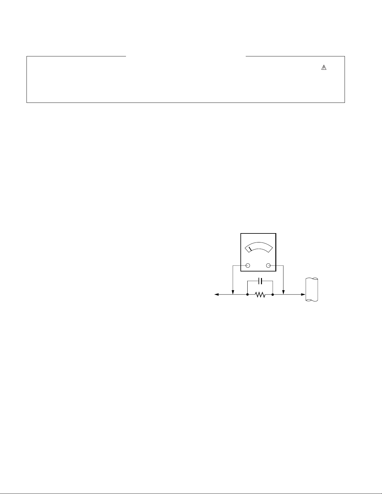
Leakage Current Hot Check (See below Figure)
Plug the AC cord directly into the AC outlet.
Do not use a line Isolation Transformer during this check.
Connect 1.5K/10watt resistor in parallel with a 0.15uF capacitor
between a known good earth ground (Water Pipe, Conduit, etc.)
and the exposed metallic parts.
Measure the AC voltage across the resistor using AC voltmeter
with 1000 ohms/volt or more sensitivity.
Reverse plug the AC cord into the AC outlet and repeat AC voltage
measurements for each exposed metallic part. Any voltage
measured must not exceed 0.75 volt RMS which is corresponds to
0.5mA.
In case any measurement is out of the limits specified, there is
possibility of shock hazard and the set must be checked and
repaired before it is returned to the customer.
Leakage Current Hot Check circuit
IMPORTANT SAFETY NOTICE
0.15uF
To Instrument's
exposed
METALLIC PARTS
AC Volt-meter
Good Earth Ground
such as WATER PIPE,
CONDUIT etc.
1.5 Kohm/10W
Page 4

- 4 -
CAUTION: Before servicing receivers covered by this service
manual and its supplements and addenda, read and follow the
SAFETY PRECAUTIONS on page 3 of this publication.
NOTE: If unforeseen circumstances create conflict between the
following servicing precautions and any of the safety precautions on
page 3 of this publication, always follow the safety precautions.
Remember: Safety First.
General Servicing Precautions
1. Always unplug the receiver AC power cord from the AC power
source before;
a. Removing or reinstalling any component, circuit board
module or any other receiver assembly.
b. Disconnecting or reconnecting any receiver electrical plug or
other electrical connection.
c. Connecting a test substitute in parallel with an electrolytic
capacitor in the receiver.
CAUTION: A wrong part substitution or incorrect polarity
installation of electrolytic capacitors may result in an
explosion hazard.
2. Test high voltage only by measuring it with an appropriate high
voltage meter or other voltage measuring device (DVM,
FETVOM, etc) equipped with a suitable high voltage probe.
Do not test high voltage by "drawing an arc".
3. Do not spray chemicals on or near this receiver or any of its
assemblies.
4. Unless specified otherwise in this service manual, clean
electrical contacts only by applying the following mixture to the
contacts with a pipe cleaner, cotton-tipped stick or comparable
non-abrasive applicator; 10% (by volume) Acetone and 90% (by
volume) isopropyl alcohol (90%-99% strength)
CAUTION: This is a flammable mixture.
Unless specified otherwise in this service manual, lubrication of
contacts in not required.
5. Do not defeat any plug/socket B+ voltage interlocks with which
receivers covered by this service manual might be equipped.
6. Do not apply AC power to this instrument and/or any of its
electrical assemblies unless all solid-state device heat sinks are
correctly installed.
7. Always connect the test receiver ground lead to the receiver
chassis ground before connecting the test receiver positive
lead.
Always remove the test receiver ground lead last.
8. Use with this receiver only the test fixtures specified in this
service manual.
CAUTION: Do not connect the test fixture ground strap to any
heat sink in this receiver.
Electrostatically Sensitive (ES) Devices
Some semiconductor (solid-state) devices can be damaged easily
by static electricity. Such components commonly are called
Electrostatically Sensitive (ES) Devices. Examples of typical ES
devices are integrated circuits and some field-effect transistors and
semiconductor "chip" components. The following techniques
should be used to help reduce the incidence of component
damage caused by static by static electricity.
1. Immediately before handling any semiconductor component or
semiconductor-equipped assembly, drain off any electrostatic
charge on your body by touching a known earth ground.
Alternatively, obtain and wear a commercially available
discharging wrist strap device, which should be removed to
prevent potential shock reasons prior to applying power to the
unit under test.
2. After removing an electrical assembly equipped with ES
devices, place the assembly on a conductive surface such as
aluminum foil, to prevent electrostatic charge buildup or
exposure of the assembly.
3. Use only a grounded-tip soldering iron to solder or unsolder ES
devices.
4. Use only an anti-static type solder removal device. Some solder
removal devices not classified as "anti-static" can generate
electrical charges sufficient to damage ES devices.
5. Do not use freon-propelled chemicals. These can generate
electrical charges sufficient to damage ES devices.
6. Do not remove a replacement ES device from its protective
package until immediately before you are ready to install it.
(Most replacement ES devices are packaged with leads
electrically shorted together by conductive foam, aluminum foil
or comparable conductive material).
7. Immediately before removing the protective material from the
leads of a replacement ES device, touch the protective material
to the chassis or circuit assembly into which the device will be
installed.
CAUTION: Be sure no power is applied to the chassis or circuit,
and observe all other safety precautions.
8. Minimize bodily motions when handling unpackaged
replacement ES devices. (Otherwise harmless motion such as
the brushing together of your clothes fabric or the lifting of your
foot from a carpeted floor can generate static electricity
sufficient to damage an ES device.)
General Soldering Guidelines
1. Use a grounded-tip, low-wattage soldering iron and appropriate
tip size and shape that will maintain tip temperature within the
range or 500
o
F to 600oF.
2. Use an appropriate gauge of RMA resin-core solder composed
of 60 parts tin/40 parts lead.
3. Keep the soldering iron tip clean and well tinned.
4. Thoroughly clean the surfaces to be soldered. Use a mall wirebristle (0.5 inch, or 1.25cm) brush with a metal handle.
Do not use freon-propelled spray-on cleaners.
5. Use the following unsoldering technique
a. Allow the soldering iron tip to reach normal temperature.
(500
o
F to 600oF)
b. Heat the component lead until the solder melts.
c. Quickly draw the melted solder with an anti-static, suction-
type solder removal device or with solder braid.
CAUTION: Work quickly to avoid overheating the
circuitboard printed foil.
6. Use the following soldering technique.
a. Allow the soldering iron tip to reach a normal temperature
(500
o
F to 600oF)
b. First, hold the soldering iron tip and solder the strand against
the component lead until the solder melts.
c. Quickly move the soldering iron tip to the junction of the
component lead and the printed circuit foil, and hold it there
only until the solder flows onto and around both the
component lead and the foil.
CAUTION: Work quickly to avoid overheating the circuit
board printed foil.
d. Closely inspect the solder area and remove any excess or
splashed solder with a small wire-bristle brush.
SERVICING PRECAUTIONS
Page 5

- 5 -
IC Remove/Replacement
Some chassis circuit boards have slotted holes (oblong) through
which the IC leads are inserted and then bent flat against the
circuit foil. When holes are the slotted type, the following technique
should be used to remove and replace the IC. When working with
boards using the familiar round hole, use the standard technique
as outlined in paragraphs 5 and 6 above.
Removal
1. Desolder and straighten each IC lead in one operation by gently
prying up on the lead with the soldering iron tip as the solder
melts.
2. Draw away the melted solder with an anti-static suction-type
solder removal device (or with solder braid) before removing the
IC.
Replacement
1. Carefully insert the replacement IC in the circuit board.
2. Carefully bend each IC lead against the circuit foil pad and
solder it.
3. Clean the soldered areas with a small wire-bristle brush.
(It is not necessary to reapply acrylic coating to the areas).
"Small-Signal" Discrete Transistor
Removal/Replacement
1. Remove the defective transistor by clipping its leads as close as
possible to the component body.
2. Bend into a "U" shape the end of each of three leads remaining
on the circuit board.
3. Bend into a "U" shape the replacement transistor leads.
4. Connect the replacement transistor leads to the corresponding
leads extending from the circuit board and crimp the "U" with
long nose pliers to insure metal to metal contact then solder
each connection.
Power Output, Transistor Device
Removal/Replacement
1. Heat and remove all solder from around the transistor leads.
2. Remove the heat sink mounting screw (if so equipped).
3. Carefully remove the transistor from the heat sink of the circuit
board.
4. Insert new transistor in the circuit board.
5. Solder each transistor lead, and clip off excess lead.
6. Replace heat sink.
Diode Removal/Replacement
1. Remove defective diode by clipping its leads as close as
possible to diode body.
2. Bend the two remaining leads perpendicular y to the circuit
board.
3. Observing diode polarity, wrap each lead of the new diode
around the corresponding lead on the circuit board.
4. Securely crimp each connection and solder it.
5. Inspect (on the circuit board copper side) the solder joints of
the two "original" leads. If they are not shiny, reheat them and if
necessary, apply additional solder.
Fuse and Conventional Resistor
Removal/Replacement
1. Clip each fuse or resistor lead at top of the circuit board hollow
stake.
2. Securely crimp the leads of replacement component around
notch at stake top.
3. Solder the connections.
CAUTION: Maintain original spacing between the replaced
component and adjacent components and the circuit board to
prevent excessive component temperatures.
Circuit Board Foil Repair
Excessive heat applied to the copper foil of any printed circuit
board will weaken the adhesive that bonds the foil to the circuit
board causing the foil to separate from or "lift-off" the board. The
following guidelines and procedures should be followed whenever
this condition is encountered.
At IC Connections
To repair a defective copper pattern at IC connections use the
following procedure to install a jumper wire on the copper pattern
side of the circuit board. (Use this technique only on IC
connections).
1. Carefully remove the damaged copper pattern with a sharp
knife. (Remove only as much copper as absolutely necessary).
2. carefully scratch away the solder resist and acrylic coating (if
used) from the end of the remaining copper pattern.
3. Bend a small "U" in one end of a small gauge jumper wire and
carefully crimp it around the IC pin. Solder the IC connection.
4. Route the jumper wire along the path of the out-away copper
pattern and let it overlap the previously scraped end of the good
copper pattern. Solder the overlapped area and clip off any
excess jumper wire.
At Other Connections
Use the following technique to repair the defective copper pattern
at connections other than IC Pins. This technique involves the
installation of a jumper wire on the component side of the circuit
board.
1. Remove the defective copper pattern with a sharp knife.
Remove at least 1/4 inch of copper, to ensure that a hazardous
condition will not exist if the jumper wire opens.
2. Trace along the copper pattern from both sides of the pattern
break and locate the nearest component that is directly
connected to the affected copper pattern.
3. Connect insulated 20-gauge jumper wire from the lead of the
nearest component on one side of the pattern break to the lead
of the nearest component on the other side.
Carefully crimp and solder the connections.
CAUTION: Be sure the insulated jumper wire is dressed so the
it does not touch components or sharp edges.
Page 6
- 6 -
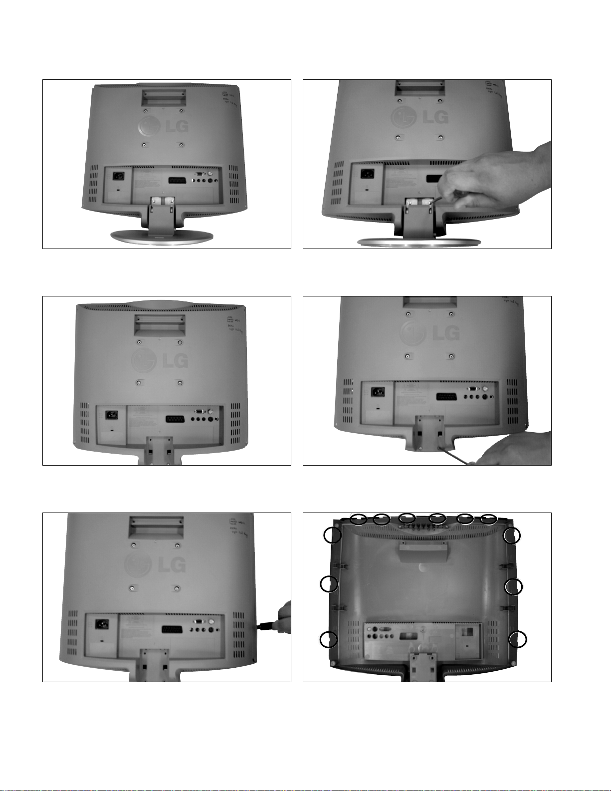
DISASSEMBLY
#1 #2 Detached stand assy (Remove the screws)
#3 Disassembly stand assy #4 Detached Backcover (Remove the screw)
#5 Open the Backcover's latch with jig #6 Unlock latch between Cabinet and Backcover
Page 7
- 7 -
SPECIFICATION
1. Application range
This specification is applied to CL-81 chassis.
2. Requirement for Test
Testing for standard of each part must be followed in below
condition.
(1) Temperature: 25°C ± 2°C
(2) Humidity: 65% ± 10%
(3) Power: Standard input voltage (AC 100-240V, 50/60Hz)
(4) Measurement must be performed after heat-run more than
30min.
(5) Adjusting standard for this chassis is followed a special
standard.
3.General Specification
3-1. 15LC1R
4. Mechanical Specification
No.
Item
Specification Remark
1
TFT Color LCD Module
20.1 inches(510.54mm) diagonal
0.2125mm(H)x0.6375mm(V)xRGB
TTL
8BIT, 16,777,216 colors
432(H) x 331.5(V) x 25(D)
Anti-Glare, Hard Coating(3H)
Normally Black
6 CCFL(6 lamps)
25ms(R.T.:12ms + F.T.:13ms)
LPL
NOTE : Specifications and others are subject to change without notice for improvement
.
No.
1 Product 15LC1R/20LC1R
Dimension Width(W) Lengh(D) Height(H)
Before Packing 377.6/492.4 242.8/272.8 394.5/483.3
After Packing 433/574.0 143/225.0 442/627.0
2 Product Only SET 5.6Kg/8.7Kg
Weight With BOX 7.7Kg/11.1Kg
Type
ActiveDisplay Area
Pixel Pitch [mm]
Electrical Interface
Color Depth
Size [mm]
Surface Treatment
Operating Mode
Back light Unit
R/T Typ.
Item
Content
Remark
No.
Item
Specification Remark
1
TFT Color LCD Module
15.0 inches(380.16mm) diagonal(Aspect 4:3)
0.297mm(H)x0.297mm(V)xRGB
LVDS
6BIT, 16,777,216 colors
332.8(H) x 262.2(V) x 18(D)
Anti-Glare(HAZE 3%), Hard Coating(3H)
Normally Black
4 CCFL(4 lamps)
R.T.:5ms + F.T.:11ms(Typ)
LPL
Type
ActiveDisplay Area
Pixel Pitch [mm]
Electrical Interface
Color Depth
Size [mm]
Surface Treatment
Operating Mode
Back light Unit
R/T Typ.
3-2. 20LC1R
Page 8
- 8 -
6.Optical Character
6-1. 15LC1R
5. Reference table-Function
No.
Item
Specification
Remark
1 Teletext TOP, FLOF NO
2 REMOCON NEC Code NTSC
3 AV Input 1 Rear
4 S-Video Input 1 Rear
5 Component Input 1 Rear
6 PERI TV Connector Full SCART : 0 NO
7 Ear-phone output 1 Rear
8 2 Carrier Stereo X
9 NICAM Stereo X
10 2 Carrier Daul X
11 NICAM Daul X
12 DW(Double Window) Mode X
13 MW(Multi Window) Mode X
14 Film Mode X
15 Noise Reduction X
16 Progressive Scan O
17 Motion Detection X
18 SRS WOW X
19 Swivel Speaker X
20 EZ-pip X
21 ARC X
22 DRP X
23 DCDI X
24 HDCP X
Item
Remark
Specification
Viewing Angle
<CR
≥
10>
Luminance
Contrast Ratio
CIE Color Coordinates
All White/All Black
In PC input
Contrast 100/Brightness 50
In AV Input
PSM : Dynamic
White
(100 IRE)
R/L,
U/D
Luminance(cd/
)
Variation
CR
Typ
65/65
45/55
400
400
0.283
0.298
0.313
0.329
0.283
0.298
0.274
0.286
Min
55/55
40/50
300
300
0.253
0.268
0.283
0.299
0.253
0.268
0.244
0.256
WHITE
(Normal)
WHITE
(Warm)
WHITE
(Normal)
WHITE
(Cool)
Wx
Wy
Wx
Wy
Wx
Wy
Wx
Wy
Max
1.3
0.313
0.328
0.343
0.359
0.313
0.328
0.304
0.316
No.
1
2
3
4
Page 9
- 9 -
7-1.General Specification
7.Engineering Specification
No Item Specification Remark
1 ENERGE-15LC1R SYNC(V/H) VIDEO POWER CONSUMPTION LED COLOE
Normal-15LC1R On/On Active ≤ 40W BLUE
Sleep Mode-15LC1R Off/On
(PC Mode) On/Off Off ≤ 1W Amber
Off/Off
Off Mode-15LC1R Off ≤ 1W Off(PC)
Amber(TV/AV)
Normal-20LC1R On/On Active ≤ 65W BLUE
Off Misw-20LC1R Off/Off Off ≤ 1W(110V) Orange
≤ 1W(220V)
2 D-SUB 1 : RED 2 : GREEN 10 : DIGITAL GND
Pin configuration 3 : BLUE 4 : ID2 (GND)
5 : S.T (GND) 6 : RED
7 : GREEN GND 8 : BLUE GND
9 : N.C 10 : D-GND
11 : ID0(GND) 12 : SDA
13 : H-SYNC 14 : V-SYNC
15 : SCL SHELL : GND
3 Control Functin 1) Contrast / Brightness
2) H-Position
3) Tracking : Clock / Phase
4) Auto Configure
5) Reset
Item RemarkSpecification
Viewing Angle
<CR
10>
Luminance
Contrast Ratio
CIE Color Coordinates
All White/All Black
In AV Input
PSM : Dynamic
White
(100 IRE)
R/L,
U/D
Luminance(cd/
)
Variation
CR
Typ
88/88
88/88
40
350
0.313
0.329
0.283
0.298
0.274
0.286
Min
85/85
85/85
300
250
0.283
0.299
0.253
0.268
0.244
0.256
WHITE
(Warm)
WHITE
(Normal)
WHITE
(Cool)
Wx
Wy
Wx
Wy
Wx
Wy
Max
1.3
0.343
0.359
0.313
0.328
0.304
0.316
No.
1
2
3
4
6-2. 20LC1R
Page 10

- 10 -
1. Application
This document is applied to 15", 20" LCD TV which is
manufactured in Monitor Factory or is produced on the basis
of this data.
2. Designation
2.1 The adjustment is according to the order which is
designated and which must be followed, according to the
plan which can be changed only on agreeing.
2.2. Power Adjustment: Free Voltage
2.3. Magnetic Field Condition: Nil.
2.4. Input signal Unit: Product Specification Standard
2.5. Reserve after operation: Above 30 Minutes
2.6. Adjustment equipments: Pattern Generator (MSPG-925
or Equivalent), DDC Adjustment Jig equipment, SVC
remote controller
3. Adjustment
3.1 APC
After Manual-Insult, executing APC
3.2 ISP UOC file
3.2.1 Required Equipment
- JIG for ISP
- PC that is installed with "WISP" program.
- Control + Power LED PCB Ass'y
3.2.2 ISP Sequence
1) Connect main board with JIG for ISP
2) Execute "WISP" Program.
3) Compare UOC version in BOM with version of hex file.
4) Push "Brouse..." button and select hex file.
5) Push " Auto Execute" button.
6) Occur an Error, push "Erase" button and try again and
again. 2)~5)
7) After finishing ISP, Must AC off / ON
8) Wait LED is not blink anymore
3.3 ADC Process
"IIC_ SW" must set "0"(After ISP, automatically set "0")
3.3.1 AV(CVBS) Mode Adjustment
3.3.1.1 Auto Gain/Offset Adjustment
Select AV(Video) in Input menu
Signal equipment : MSPG925
Output Jack : CVBS
Output Voltage : 700 mVp-p (patt # 29 in MSPG925)
Resolution : NTSC J - 720 x 480 @59,94Hz (Model
#207 in MSPG925)
Adjust by commanding AUTO_COLOR_ADJUST
(0xF1) 0x00 0x00 instruction.
3.3.1.2 Confirmation of adjustment process
We confirm whether "0x01" address of EEPROM
"0xA0" is "0xAA" or not.
If "0x01" address of EEPROM "0xA0" isn't "0xAA", we
adjust once more in adjustment line by adjust method
of 3.2.1.2.
We can confirm the ADC values from "0x0C~0x11"
addresses in a page "0xA0"
3.3.2 Component Mode Adjustment
3.3.2.1 Auto Gain/Offset Adjustment
Select Component in Input menu
Signal equipment : MSPG925
Output Jack : D4(Japan) or Componen(Except Japan)
Output Voltage : 700 mVp-p (patt # 8 in MSPG925)
Resolution 483/60P - 720 x 483p @59.94Hz (Model
#212 in MSPG925)
Adjust by commanding AUTO_COLOR_ADJUST
(0xF1) 0x00 0x00 instruction.
3.3.2.2 Confirmation of adjustment process
We confirm whether "0x01" address of EEPROM
"0xA0" is "0xAA" or not.
If "0x01" address of EEPROM "0xA0" isn't "0xAA", we
adjust once more in adjustment line by adjust method
of 3.2.1.2.
We can confirm the ADC values from "0x??~0x??"
addresses in a page "0xA0"
*Caution*
If DDC CMD don't work, please check below.
1. Enter SVC menu by SVC Remote controller
2. Enter "ETC" menu
Check please, IIC_SW is "0" or "1".
- IIC_SW "0" : DDC Communications.(DDC2AB)
- IIC_SW "1" : EDID Write/Read (DDC2B) and Factory
default.
3.4 Function Check
3.4.1 Check display and sound
"IIC_ SW" must set "1"
Check Input and Signal items. (cf. work instructions)
1. TV
2. AV (CVBS/ S-Video)
3 Component
4. H/P Out
3.4.2 DCXO setting
: After finished all function check, "IIC_ SW" must set "0" by
pushing "TILT" key in SVC remocon
ADJUSTMENT INSTRUCTION
Page 11

- 11 -
4. Total Assembly line process
4.1 Adjustment Preparation
"IIC_ SW" must set "0"
Above 30 minutes H/run in RF no signal
15 Pin D-Sub Jack is connected to the signal of
Pattern Generator.
4.2 Confirmation of Luminance
Set Statement
Input : CVBS
Contrast : 100(Max)
Brightness : 50
CSM : Normal
Signal equipment displays
Output Voltage : 700 mVp-p
Output Mode : Full White pattern (100 IRE)
Confirm whether luminance is over 300cd or not
4.3 Confirmation of Color Coordinate
Input Full White Pattern
Set CSM : Normal (9300K)
Confirm whether x = 0.283±0.03, y=0.298±0.03 or not
Set CSM : Warm (6500K)
Confirm whether color coordinate is x= 0.313±0.03,
y=0.329±0.03 or not
Set CSM : Warm (11000K)
Confirm whether color coordinate is x= 0.274±0.03,
y=0.286±0.03 or not
After confirming Color coordinates, Must return to
Normal
* After Confirming color coordinate and luminance, "IIC_ SW"
must set "1"
Page 12

- 12 -
5. Outgoing Condition
ITEM Outgoing Condigion Remarks
Outgoing Input Source TV
Condition Volume Level 30
Power S/W Off
Channel EZ scan To Start
Manual Program TV 2
Erase
Fine 0
Ficture EZ Video Clear
ACC Normal
Sound AVL Off
Balance 0
Timer Clock Auto
Off Timer --:--
Off
On Timer --:--
TV 2
Volume 30
Off
Auto Off Off
Special Language English
Input TV
Key lock Off
Power indicator On
Caption/Text CC1 Canada/
Captions Off USA Only
Parental To set (Code : 0000)
Screen Auto Configure To Set Only
Manual Configure To Set RGB PC
Reset To Set INPUT
Page 13

- 13 -
SVC REMOCON
NO. KEY FUNTION REMARK
1 POWER To turn the TV on or off
2 MUTE To activate the mute function.
3 P-CHECK To check TV screen image easily. Shortcut keys
4 S-CHECK To check TV screen sound easily Shortcut keys
5 ARC(23inch) To select size of the main screen Shortcut keys
(Auto, 4:3, 16:9, 14:3, Zoom, Cinema Zoom)
6 CAPTION Switch to closed caption broadcasting
7 TXT To toggle on/off the teletext mode
8 TV/AV External input
9 IN-START To enter adjustment mode when manufacturing the TV sets.
Use the AV key to
In-Start
Vol±
Auto ADC
Vol±
W/B adjustment
enter the screen W/B
Exit two times(Adjustment completed)
adjustment mode.
10 MPX To select the multiple sound mode
(Mono, Stereo or MPEG, DOLBY, Digital)
11 EXIT To release the adjustment mode
12 APC(PSM)
To easily adjust the screen according to surrounding brightness
13 ASC(SSM) To easily adjust sound according to the program type
14 MULTIMEDIA External input Shortcut keys
15 CH ±
To move channel up/down or to select a functiondisplayed on the screen.
16 VOL ± To adjust the volume or accurately control a specific function.
17 ENTER To set a specific function or complete setting.
18 CH-(OP1) To use as a red key in the teletext mode
19 CH+(OP2) To use as a green key in the teletext mode
20 SWAP(OP3) To use as a yellow key in the teletext mode
21 INPUT(OP4) To use as a blue key in the teletext mode
22 MENU
To select the functions such as video, voice, function or channel.
23 IN-STOP
To set the delivery condition status after manufacturing the TV set.
24 HOLD
Used as a hold key in the teletext mode (Page updating is stopped.)
25 TIME Displays the teletext time in the normal mode
Enables to select the sub code in the teletext mode
26 SIZE Used as the size key in the teletext mode
27 INDEX Used as the index key in the teletext mode
(Top index will be displayed if it is the top text.)
28 UPDATE Used as the update key in the teletext mode
(Text will be displayed if the current page is updated.)
29 MODE Used as Mode in the teletext mode
30 TILT
To set IIC SW "0" or "1" in the adjustment mode
31 0~9 To manually select the channel.
Page 14

- 14 -
TROUBLESHOOTING
No power
(LED indicator off)
Check short of main B/D
or Change Lips
Change U406
Change LED Assy
Check 15V or 5V
of Lips
Check Output of
U406
Check LED Assy
Check J103, J125, J126
Connector
Fail
Fail
Change Q402
Check Output of
Q402
Fail
Pass
Fail
Pass
Pass
Pass
:[A]Process
Page 15

- 15 -
No Raster
Check LED Status
on display unit
Check the input/
Output of U301
Check
U401~U405, U407, U409
Check inverter
Connector or inverter
Check input source cable and jack
Repeat [A] PROCESS
Fail
Change U401~U405,
U407, U409
Fail
Change U301
Fail
Change inverter
connector or inverter
Fail
Change panel link
cable or module
Fail
Check panel link
Cable or module
Pass
Pass
Pass
Pass
Pass
:[B]Process
Page 16

- 16 -
No Raster on AV Signal
(Component, CVBS, S-VHS)
No Raster on TV(RF) signal
Change Q113, Q114,
Q115, R194, R198, R184
Check the signal of
Q113, Q114, Q115
R194, R198, R184
Repeat
[A] Process
Check the output of
TU701
Check the
input/output of U301
Check the
input/output of U101
Check input source cable and jack
Fail
Fail
Fail
Fail
Re-soldering or
Change the defect part
Check X301
Fail
Re-soldering or
Change the defect part
Check 5V, 33V of TU701
Re-soldering or
Change the defect part
Pass
Pass
Pass
Pass
Page 17

- 17 -
No Sound
Check the speaker wire
Change source input
Check the
input source
Fail
Pass
Re-soldering or
Change the defect part
Check X301
Check the input/output
of U301
Fail
Pass
Re-soldering or
Change the defect part
Check the input/output
of U201
Fail
Pass
Change speaker
Check the speaker
Fail
Pass
Page 18

- 18 -
BLOCK DIAGRAM
Page 19

- 19 -
BLOCK DIAGRAM DESCRIPTION
Power Supply Block (LIPS)
This Block Generates DC Voltage (5V,15V) to Main
Control system from AC Power (100-240 V, 50/60 Hz,
1.0A)
Also it has the inverter function that converts input
voltage to AC Rms value for the LCD lamp.
DC/DC Converter block
DC/DC Converter convert the input 5V,15V to proper
3.3V, 5V, 8V, 12V for Main control system.
For shooting heat trouble, we use the DC/DC
converting IC
Audio Amplifier
This block is composed of TPA3005D2 and peripheral
device.
The function of the audio amplifier is that to amplify
audio L / R signal transmitted from audio decoder. The
audio signal is amplified according to pre-defined DC
volume control curve.
Audio / Video / IF Decoder / Scaler
This block is composed of LOC1 and peripheral
devices.
1) Video Decoder
This Block Selects input Video signals (like CVBS, Y/C,
SCART RGB) and output RGB signal.
On decoding, We can control signal like Contrast,
Brightness, Sharpness, Color, tint signals including
Adaptive Comb Filter
2) Audio Decoder
This block analyzes audio input signal through A/V Jack
and PC audio and Tuner IF.
The analyzed signals transmitted to audio amplifier
On decoding, We can control signal like Bass, treble.
3) IF Decoder
This block can change IF signal to audio and video
signal that transmitted to Video/audio decoder.
4) Scaler
This IC includes A/D Converter and LVDS Transmitter
This IC is directly Inputted Analog Signal and transmits
it to LCD Module
5) Micom
This block controls each IC through IIC communication
line.
LVDS Rx (DTC34LF86L)
It is composed of DTC34LF86L/THC63LVDF84B.
The LVDS Rx converts the LVDS data streams back
into 24bits of CMOS/TTL data with
Falling edge or rising edge clock for convenient with
variety of LCD panel controllers.
Switch IC (PI3V512QE)
It is composed of PI3V512QE.
This IC selects between D-sub RGB signal and LOC1
RGB signal, and it transmits the selected signal to
video signal processor.
TUNER
Micom controls this through IIC Line.
TUNER makes IF and transmits IF signal to LOC1.
Page 20

- 20 -
WIRING DIAGRAM
6631T20042B-11P(15LC1RB)
6631T20034M-11P(20LC1RB)
6631T20010F-3P(15LC1RB)
6631T20037Q-3P(20LC1RB)
2
5
INTERFACE BOARD
Only 20LC1R*_LPL Module
6631900037B-50P(20LC1RB)
1
6631900037A-50P(20LC1RB, LPL)
6631T20012R-20P(15LC1RB)
6631900024D-3P
3
6631900026A-4P(20LC1RB)
663190002B-4P(15LC1RB)
6
6631T20029S-5P
4
6631900026A-4P(20LC1RB)
6
6631900026B-4P(15LC1RB)
Page 21

- 21 -
EXPLODED VIEW
030
040
042
041
070
060
010
100
090
080
020
130
120
110
050
Page 22

- 22 -
EXPLODED VIEW PARTS LIST
No. PART NO.
DESCRIPTION
30919B0002M CABINET ASSEMBLY, 15LC1R BRAND . NORTH AMERICA(BK, SET)
30919B0002J CABINET ASSEMBLY, 15LC1R-MG BRAND . NORTH AMERICA-CSKD
30919D0001G CABINET ASSEMBLY, 20LC1R-MG(BK) BRAND 3090TKD006 SET
30919D0001H CABINET ASSEMBLY, 20LC1R-MG(BK) BRAND 3090TKD006 C/SKD
6304FLP234A LCD(LIQUID CRYSTAL DISPLAY), LC150X02-TL01 LG PHILPS TFT COLOR TN LAMP MULTI
6304FLP188A
LCD(LIQUID CRYSTAL DISPLAY), LC201V02-A3KA LG PHILPS TFT COLOR PB FREE MODULE , SS D-IC
3809900013E BACK COVER ASSEMBLY, 15LC1 2PHONE FOR N.A
3809900002L BACK COVER ASSEMBLY, 20LC1R-MG(USA) NON SET(BK)
3809900002M BACK COVER ASSEMBLY, 20LC1R-MG(USA) NON C/SKD(BK)
3043900003F TILT SWIVEL ASSEMBLY, 15LC1R-MG 49509K0009A N/A NO PRINTNG
3043900002B TILT SWIVEL ASSEMBLY, 20LC1R-ZB 3550TKK974
3043900039A TILT SWIVEL ASSEMBLY, 15LC1 . STAND BODY ASSY-CSKD
3043900010B TILT SWIVEL ASSEMBLY, 20LC1RB-ZG NON HINGE ASSY(BK)-CSKD
3043900040C TILT SWIVEL ASSEMBLY, 15LC1R-MG(N/A) . STAND BASE ASSY(BK, NO PRINT)-CSKD
3043900011B TILT SWIVEL ASSEMBLY, 20LC1 NON STAND BASE ASSY(FOR USA)-CSKD
68719ST799B PWB(PCB) ASSEMBLY,SUB, SUB T.T CL81 LC1R ALEULFX LED
68719ST799E PWB(PCB) ASSEMBLY,SUB, SUB T.T CL81 20LC1R-ZG SLEELFP LED+IR-CSKD
68719ST801A PWB(PCB) ASSEMBLY,SUB, SUB T.T CL81 1XLC1 ANEULFX CONTROL
68719ST956A PWB(PCB) ASSEMBLY,SUB, SUB T.T CL81 15LC1R SNRULFT CONTROL-CSKD
68719ST798A PWB(PCB) ASSEMBLY,SUB, SUB T.T CL81 2XLC1 ALEULFX CONTROL
68719ST798B PWB(PCB) ASSEMBLY,SUB, SUB T.T CL81 2XLC1 SLEELFP CONTROL-CSKD
49519S0004B METAL ASSEMBLY, FRAME, MAIN ASSY-15LC1-LPL-TN
49519S0004F METAL ASSEMBLY, FRAME, MAIN ASSY-15LC1-LPL TN C/SKD
49519S0001A METAL ASSEMBLY, FRAME, 20LC1
49519S0001B METAL ASSEMBLY, FRAME, 20LC1R-ZB(C/SKD)
6871TPT318B PWB(PCB) ASSEMBLY,POWER, MFT 4-LAMP POWER TOTAL BRAND . 15LC1R
6871TPT319A PWB(PCB) ASSEMBLY,POWER, 6-LAMP TV/MNT/MFT POWER TOTAL BRAND .-20LC1R
33139N1011C MAIN TOTAL ASSEMBLY, 15LC1R-MG BRAND CL-81(USA)
33139N1015A MAIN TOTAL ASSEMBLY, 15LC1RX-MG(SKD) BRAND CL-81
33139N2021A MAIN TOTAL ASSEMBLY, 20LC1R-MG(C) BRAND CL-81
33139N2021C MAIN TOTAL ASSEMBLY, 20LC1R-MG SKD(C) BRAND CL-81
49519K0117B METAL ASSEMBLY, SHIELD, AV NTSC 15LC1
49519K0117E METAL ASSEMBLY, SHIELD, 15LC1R-MG(NTSC, USA) AV SHIELD PHANTOM-20LC1R
6400GTTX02A
SPEAKER,FULLRANGE, EF1527C-6428-6 TOPTONE FULL-RANGE(GENERAL) 16OHM 5/7W 82DB OTHERS 40*70 210HZ
68719ST077A PWB(PCB) ASSEMBLY,SUB, SUB T.T CL81 20LC1R ALEULFX HIROSE-ONLY 20LC1R
68719ST077B
PWB(PCB) ASSEMBLY,SUB, SUB T.T CL81 20LC1R SLEELFP INTERFACE(HIROSE)-ONLY 20LC1R, CSKD
49519K0116A METAL ASSEMBLY, REAR 15LC1
49519K0116B METAL ASSEMBLY, REAR 15LC1 C/SKD
4950TKA372A METAL, SHIELD, MAIN 20LC1
4950TKA372D METAL, SHIELD, MAIN 20LC1, C/SKD
010
020
030
040
041
042
050
060
070
080
090
100
110
120
130
Page 23

- 23 -
DATE: 2006. 01. 20.
*S *AL LOC. NO. PART NO. DESCRIPTION / SPECIFICATION
C301 0CH3224K946 0.22UF 50V Z F 2012 R/TP
C307 0CH3224K946 0.22UF 50V Z F 2012 R/TP
C3092 0CH3224K946 0.22UF 50V Z F 2012 R/TP
C316 0CH3224K946 0.22UF 50V Z F 2012 R/TP
C319 0CH3224K946 0.22UF 50V Z F 2012 R/TP
C322 0CH3224K946 0.22UF 50V Z F 2012 R/TP
C327 0CH3224K946 0.22UF 50V Z F 2012 R/TP
C330 0CH3224K946 0.22UF 50V Z F 2012 R/TP
C367 0CH3224K946 0.22UF 50V Z F 2012 R/TP
C394 0CH3224K946 0.22UF 50V Z F 2012 R/TP
C395 0CH3224K946 0.22UF 50V Z F 2012 R/TP
C102 0CH3104K566 0.1UF 50V 10% X7R 2012 R/TP-15LC1R
C111 0CK105DH56A 1UF 2012 25V 10% X7R R/TP-15LC1R
C112 0CK105DH56A 1UF 2012 25V 10% X7R R/TP-15LC1R
C113 0CH5220K416 22PF 50V 5% NP0 2012 R/TP-15LC1R
C114 0CH5470K416 47PF 50V 5% NP0 2012 R/TP-15LC1R
C115 0CH5470K416 47PF 50V 5% NP0 2012 R/TP-15LC1R
C116 0CH5101K416 100PF 50V 5% NP0 2012 R/TP-15LC1R
C124 0CH3104K566 0.1UF 50V 10% X7R 2012 R/TP
C132 0CH3104K566 0.1UF 50V 10% X7R 2012 R/TP
C144 0CK105DH56A 1UF 2012 25V 10% X7R R/TP
C174 0CH3104K566 0.1UF 50V 10% X7R 2012 R/TP
C176 0CH3104K566 0.1UF 50V 10% X7R 2012 R/TP
C177 0CH3104K566 0.1UF 50V 10% X7R 2012 R/TP
C178 0CH3104K566 0.1UF 50V 10% X7R 2012 R/TP
C180 0CK475DD57A 4.7UF 2012 10V 10% X5R R/TP
C181 0CK475DD57A 4.7UF 2012 10V 10% X5R R/TP
C183 0CH3104K566 0.1UF 50V 10% X7R 2012 R/TP
C184 0CH3104K566 0.1UF 50V 10% X7R 2012 R/TP
C185 0CH3104K566 0.1UF 50V 10% X7R 2012 R/TP
C187 0CH3104K566 0.1UF 50V 10% X7R 2012 R/TP
C188 0CH3104K566 0.1UF 50V 10% X7R 2012 R/TP
C190 0CH3104K566 0.1UF 50V 10% X7R 2012 R/TP
C192 0CH3104K566 0.1UF 50V 10% X7R 2012 R/TP
C197 0CH3104K566 0.1UF 50V 10% X7R 2012 R/TP
C205 0CH3474H946 "0.47UF 25V 80%,-20% F(Y5V)"
C209 0CH3474H946 "0.47UF 25V 80%,-20% F(Y5V)"
C211 0CH3104K566 0.1UF 50V 10% X7R 2012 R/TP
C212 0CH3104K566 0.1UF 50V 10% X7R 2012 R/TP
C213 0CH3474H946 "0.47UF 25V 80%,-20% F(Y5V)"
C215 0CH3474H946 "0.47UF 25V 80%,-20% F(Y5V)"
C216 0CH3104K566 0.1UF 50V 10% X7R 2012 R/TP
C217 0CH3104K566 0.1UF 50V 10% X7R 2012 R/TP
C228 0CH3474H946 "0.47UF 25V 80%,-20% F(Y5V)"
C236 0CH5102K416 1000PF 50V 5% NP0 2012 R/TP
C237 0CH5102K416 1000PF 50V 5% NP0 2012 R/TP
C238 0CH5102K416 1000PF 50V 5% NP0 2012 R/TP
C239 0CH5102K416 1000PF 50V 5% NP0 2012 R/TP
C240 0CH3474H946 "0.47UF 25V 80%,-20% F(Y5V)"
C3001 0CH3104K566 0.1UF 50V 10% X7R 2012 R/TP
C3002 0CH3104K566 0.1UF 50V 10% X7R 2012 R/TP
C3011 0CH3103K516 10000PF 50V 10% B(Y5P) 2012
C3012 0CH5470K416 47PF 50V 5% NP0 2012 R/TP-15LC1R
DATE: 2006. 01. 20.
*S *AL LOC. NO. PART NO. DESCRIPTION / SPECIFICATION
C3012 0CH6470K416 47PF 2012 50V 5% NP0 R/TP-20LC1R
C3013 0CH3104K566 0.1UF 50V 10% X7R 2012 R/TP
C3014 0CH5470K416 47PF 50V 5% NP0 2012 R/TP-15LC1R
C3014 0CH6470K416 47PF 2012 50V 5% NP0 R/TP-20LC1R
C3022 0CH3474H946 "0.47UF 25V 80%,-20% F(Y5V)"
C3024 0CH5470K416 47PF 50V 5% NP0 2012 R/TP-15LC1R
C3024 0CH6470K416 47PF 2012 50V 5% NP0 R/TP-20LC1R
C3026 0CH3474H946 "0.47UF 25V 80%,-20% F(Y5V)"
C3028 0CH5470K416 47PF 50V 5% NP0 2012 R/TP-15LC1R
C3028 0CH6470K416 47PF 2012 50V 5% NP0 R/TP-20LC1R
C3033 0CH5470K416 47PF 50V 5% NP0 2012 R/TP-15LC1R
C3033 0CH6470K416 47PF 2012 50V 5% NP0 R/TP-20LC1R
C3043 0CH5470K416 47PF 50V 5% NP0 2012 R/TP-15LC1R
C3043 0CH6470K416 47PF 2012 50V 5% NP0 R/TP-20LC1R
C3051 0CH3104K566 0.1UF 50V 10% X7R 2012 R/TP
C3061 0CH3104K566 0.1UF 50V 10% X7R 2012 R/TP
C3062 0CH5470K416 47PF 50V 5% NP0 2012 R/TP-15LC1R
C3062 0CH6470K416 47PF 2012 50V 5% NP0 R/TP-20LC1R
C3082 0CK225DH94A "2.2UF 2012 25V 80%,-20% F(Y"
C3083 0CK225DH94A "2.2UF 2012 25V 80%,-20% F(Y"
C3084 0CH3104K566 0.1UF 50V 10% X7R 2012 R/TP
C3093 0CH3104K566 0.1UF 50V 10% X7R 2012 R/TP
C3102 0CK475DD57A 4.7UF 2012 10V 10% X5R R/TP
C313 0CH3104K566 0.1UF 50V 10% X7R 2012 R/TP
C331 0CH3103K516 10000PF 50V 10% B(Y5P) 2012
C332 0CH3104K566 0.1UF 50V 10% X7R 2012 R/TP
C334 0CH3104K566 0.1UF 50V 10% X7R 2012 R/TP
C335 0CH3104K566 0.1UF 50V 10% X7R 2012 R/TP
C336 0CH3104K566 0.1UF 50V 10% X7R 2012 R/TP
C337 0CH3104K566 0.1UF 50V 10% X7R 2012 R/TP
C338 0CH3104K566 0.1UF 50V 10% X7R 2012 R/TP
C339 0CH3104K566 0.1UF 50V 10% X7R 2012 R/TP
C340 0CH3104K566 0.1UF 50V 10% X7R 2012 R/TP
C341 0CH3104K566 0.1UF 50V 10% X7R 2012 R/TP
C342 0CH3104K566 0.1UF 50V 10% X7R 2012 R/TP
C343 0CH3104K566 0.1UF 50V 10% X7R 2012 R/TP
C347 0CH3104K566 0.1UF 50V 10% X7R 2012 R/TP
C348 0CH3104K566 0.1UF 50V 10% X7R 2012 R/TP
C350 0CH3104K566 0.1UF 50V 10% X7R 2012 R/TP
C358 0CH3104K566 0.1UF 50V 10% X7R 2012 R/TP
C360 0CH3104K566 0.1UF 50V 10% X7R 2012 R/TP
C361 0CH3104K566 0.1UF 50V 10% X7R 2012 R/TP
C362 0CH3104K566 0.1UF 50V 10% X7R 2012 R/TP
C363 0CH3104K566 0.1UF 50V 10% X7R 2012 R/TP
C364 0CH3104K566 0.1UF 50V 10% X7R 2012 R/TP
C365 0CH3104K566 0.1UF 50V 10% X7R 2012 R/TP
C366 0CH3104K566 0.1UF 50V 10% X7R 2012 R/TP
C370 0CH3223K516 22000PF 2012 50V 10% B(Y5P)
C373 0CH3104K566 0.1UF 50V 10% X7R 2012 R/TP
C374 0CH3104K566 0.1UF 50V 10% X7R 2012 R/TP
C375 0CH3104K566 0.1UF 50V 10% X7R 2012 R/TP
C379 0CH5102K416 1000PF 50V 5% NP0 2012 R/TP
C386 0CH3104K566 0.1UF 50V 10% X7R 2012 R/TP
C388 0CH3104K566 0.1UF 50V 10% X7R 2012 R/TP
REPLACEMENT PARTS LIST
MAIN BOARD
CAPACITOR
For Capacitor & Resistors, the
charactors at 2nd and 3rd digit in the
P/No. means as follows;
CC, CX, CK, CN, CH : Ceramic
CQ : Polyestor
CE : Electrolytic
CF : Fixed Film
RD : Carbon Film
RS : Metal Oxide Film
RN : Metal Film
RH : CHIP, Metal Glazed(Chip)
RR : Drawing
Page 24

- 24 -
DATE: 2006. 01. 20.
*S *AL LOC. NO. PART NO. DESCRIPTION / SPECIFICATION
C389 0CH3104K566 0.1UF 50V 10% X7R 2012 R/TP
C390 0CH3104K566 0.1UF 50V 10% X7R 2012 R/TP
C391 0CH3104K566 0.1UF 50V 10% X7R 2012 R/TP
C396 0CH3104K566 0.1UF 50V 10% X7R 2012 R/TP
C403 0CH3104K566 0.1UF 50V 10% X7R 2012 R/TP
C409 0CH3104K566 0.1UF 50V 10% X7R 2012 R/TP
C411 0CK475DD57A 4.7UF 2012 10V 10% X5R R/TP
C413 0CH3103K516 10000PF 50V 10% B(Y5P) 2012
C415 0CK105DH56A 1UF 2012 25V 10% X7R R/TP
C416 0CH3104K566 0.1UF 50V 10% X7R 2012 R/TP
C421 0CH3104K566 0.1UF 50V 10% X7R 2012 R/TP
C422 0CH3104K566 0.1UF 50V 10% X7R 2012 R/TP
C425 0CH3105H946 "1UF 2012 25V 80%,-20% F(Y5V"
C704 0CH3104K566 0.1UF 50V 10% X7R 2012 R/TP
C705 0CH3104K566 0.1UF 50V 10% X7R 2012 R/TP
C708 0CH3104K566 0.1UF 50V 10% X7R 2012 R/TP
C744 0CH3104K566 0.1UF 50V 10% X7R 2012 R/TP
C110 0CK104CK56A 0.1UF 1608 50V 10% R/TP X7R
C117 0CK105DH56A 1UF 2012 25V 10% X7R R/TP
C118 0CK105DH56A 1UF 2012 25V 10% X7R R/TP
C129 0CK104CK56A 0.1UF 1608 50V 10% R/TP X7R-15LC1R
C130 0CK104CK56A 0.1UF 1608 50V 10% R/TP X7R-15LC1R
C131 0CK104CK56A 0.1UF 1608 50V 10% R/TP X7R-15LC1R
C145 0CK103CK51A 0.01UF 1608 50V 10% R/TP B(
C202 0CK104CK56A 0.1UF 1608 50V 10% R/TP X7R
C203 0CK104CK56A 0.1UF 1608 50V 10% R/TP X7R
C206 0CK224CF56A 0.22UF 1608 16V 10% R/TP X7
C207 0CK105CF94A "1UF 1608 16V 80%,-20% R/TP"
C208 0CK105CF94A "1UF 1608 16V 80%,-20% R/TP"
C210 0CK224CF56A 0.22UF 1608 16V 10% R/TP X7
C214 0CK224CF56A 0.22UF 1608 16V 10% R/TP X7
C218 0CK224CF56A 0.22UF 1608 16V 10% R/TP X7
C221 0CK474CH94A "0.47UF 1608 25V 80%,-20% R/"
C222 0CK474CH94A "0.47UF 1608 25V 80%,-20% R/"
C223 0CK105CF94A "1UF 1608 16V 80%,-20% R/TP"
C224 0CK474CH94A "0.47UF 1608 25V 80%,-20% R/"
C225 0CK474CH94A "0.47UF 1608 25V 80%,-20% R/"
C3015 0CK474CH94A "0.47UF 1608 25V 80%,-20% R/"
C3017 0CK474CH94A "0.47UF 1608 25V 80%,-20% R/"
C3019 0CK104CK56A 0.1UF 1608 50V 10% R/TP X7R
C302 0CK104CK56A 0.1UF 1608 50V 10% R/TP X7R
C303 0CK104CK56A 0.1UF 1608 50V 10% R/TP X7R
C3031 0CK474CH94A "0.47UF 1608 25V 80%,-20% R/"
C3032 0CK474CH94A "0.47UF 1608 25V 80%,-20% R/"
C3035 0CK225DH94A "2.2UF 2012 25V 80%,-20% F(Y"
C3036 0CK333CK56A 33000PF 1608 50V 10% R/TP X
C304 0CK224CF56A 0.22UF 1608 16V 10% R/TP X7
C3040 0CK225DH94A "2.2UF 2012 25V 80%,-20% F(Y"
C3042 0CK104CK56A 0.1UF 1608 50V 10% R/TP X7R
C3044 0CK333CK56A 33000PF 1608 50V 10% R/TP X
C3047 0CK474CH94A "0.47UF 1608 25V 80%,-20% R/"
C3050 0CK333CK56A 33000PF 1608 50V 10% R/TP X
C3064 0CK474CH94A "0.47UF 1608 25V 80%,-20% R/"
C3066 0CK104CK56A 0.1UF 1608 50V 10% R/TP X7R
C3068 0CK333CK56A 33000PF 1608 50V 10% R/TP X
C3069 0CK333CK56A 33000PF 1608 50V 10% R/TP X
C3070 0CK333CK56A 33000PF 1608 50V 10% R/TP X
C3085 0CK225DH94A "2.2UF 2012 25V 80%,-20% F(Y"
C3086 0CK225DH94A "2.2UF 2012 25V 80%,-20% F(Y"
C3090 0CK104CK56A 0.1UF 1608 50V 10% R/TP X7R
C3091 0CK474CH94A "0.47UF 1608 25V 80%,-20% R/"
C312 0CK104CK56A 0.1UF 1608 50V 10% R/TP X7R
DATE: 2006. 01. 20.
*S *AL LOC. NO. PART NO. DESCRIPTION / SPECIFICATION
C320 0CK104CK56A 0.1UF 1608 50V 10% R/TP X7R
C345 0CK224CF56A 0.22UF 1608 16V 10% R/TP X7
C352 0CK224CF56A 0.22UF 1608 16V 10% R/TP X7
C354 0CK104CK56A 0.1UF 1608 50V 10% R/TP X7R
C355 0CK104CK56A 0.1UF 1608 50V 10% R/TP X7R
C356 0CK104CK56A 0.1UF 1608 50V 10% R/TP X7R
C357 0CK104CK56A 0.1UF 1608 50V 10% R/TP X7R
C369 0CK224CF56A 0.22UF 1608 16V 10% R/TP X7
C372 0CK104CK56A 0.1UF 1608 50V 10% R/TP X7R
C380 0CK104CK56A 0.1UF 1608 50V 10% R/TP X7R
C381 0CK104CK56A 0.1UF 1608 50V 10% R/TP X7R
C382 0CK104CK56A 0.1UF 1608 50V 10% R/TP X7R
C387 0CK104CK56A 0.1UF 1608 50V 10% R/TP X7R
C392 0CK104CK56A 0.1UF 1608 50V 10% R/TP X7R
C706 0CK103CK51A 0.01UF 1608 50V 10% R/TP B(
C707 0CK103CK51A 0.01UF 1608 50V 10% R/TP B(
C710 0CK103CK51A 0.01UF 1608 50V 10% R/TP B(
C156 0CH6680K416 68PF 2012 50V 5% NP0 R/TP-15LC1R
C191 0CH6331K416 330PF 2012 50V 5% NP0 R/TP
C305 0CH6151K416 150PF 2012 50V 5% NP0 C3060 0CH2392K516 3900PF 50V 10% B(Y5P) 2012
C317 0CH2472K516 4700PF 50V 10% B(Y5P) 2012
C329 0CH2334F566 0.33UF 16V 10% X7R 2012 R/T
C383 0CH2222K516 2200PF 50V 10% B(Y5P) 2012
C126 0CC101CK41A 100PF 1608 50V 5% R/TP NP0-15LC1R
C127 0CC101CK41A 100PF 1608 50V 5% R/TP NP0-15LC1R
C153 0CC101CK41A 100PF 1608 50V 5% R/TP NP0-15LC1R
C154 0CC101CK41A 100PF 1608 50V 5% R/TP NP0-15LC1R
C155 0CC470CK41A 47PF 1608 50V 5% R/TP NP0
C157 0CC470CK41A 47PF 1608 50V 5% R/TP NP0
C163 0CC330CK41A 33PF 1608 50V 5% R/TP NP0
C165 0CC330CK41A 33PF 1608 50V 5% R/TP NP0
C167 0CC330CK41A 33PF 1608 50V 5% R/TP NP0
C189 0CC271CK41A 270PF 1608 50V 5% R/TP NP0
C198 0CC271CK41A 270PF 1608 50V 5% R/TP NP0
C199 0CC271CK41A 270PF 1608 50V 5% R/TP NP0
C204 0CC221CK41A 220PF 1608 50V 5% R/TP NP0
C232 0CC470CK41A 47PF 1608 50V 5% R/TP NP0
C233 0CC470CK41A 47PF 1608 50V 5% R/TP NP0
C3030 0CC470CK41A 47PF 1608 50V 5% R/TP NP0
C3037 0CC150CK41A 15PF 1608 50V 5% R/TP NP0
C3045 0CC470CK41A 47PF 1608 50V 5% R/TP NP0
C3048 0CC470CK41A 47PF 1608 50V 5% R/TP NP0
C3049 0CC150CK41A 15PF 1608 50V 5% R/TP NP0
C3073 0CC150CK41A 15PF 1608 50V 5% R/TP NP0
C308 0CC150CK41A 15PF 1608 50V 5% R/TP NP0
C3080 0CC470CK41A 47PF 1608 50V 5% R/TP NP0
C3081 0CC470CK41A 47PF 1608 50V 5% R/TP NP0
C309 0CC150CK41A 15PF 1608 50V 5% R/TP NP0
C3100 0CC101CK41A 100PF 1608 50V 5% R/TP NP0
C3101 0CC270CK41A 27PF 1608 50V 5% R/TP NP0
C376 0CC470CK41A 47PF 1608 50V 5% R/TP NP0
C377 0CC470CK41A 47PF 1608 50V 5% R/TP NP0
C378 0CC470CK41A 47PF 1608 50V 5% R/TP NP0
C393 0CC100CK41A 10PF 1608 50V 5% R/TP NP0
C412 0CC102CK41A 1000PF 1608 50V 5% R/TP NP0
C134 0CE228ED618 "2200UF KMG,RD 10V 20% FL TA"
C146 0CE108EH618 1000UF KMG 25V 20% FL TP 5
C226 0CE477EH618 470UF KMG 25V 20% FL TP 5
C227 0CE477EH618 470UF KMG 25V 20% FL TP 5
C405 0CE477ED610 "470UF KMG,RD 10V 20% FL BUL"
C748 0CE226EK610 "22UF KMG,RD 50V 20% FL BULK"
Page 25

DATE: 2006. 01. 20.
*S *AL LOC. NO. PART NO. DESCRIPTION / SPECIFICATION
C101 0CE107WF6DC 100UF MVK 16V 20% R/TP(SMD)
C162 0CH8106F691 10UF 16V 20% 105STD (CYL) R
C164 0CH8106F691 10UF 16V 20% 105STD (CYL) R
C166 0CH8106F691 10UF 16V 20% 105STD (CYL) R
C175 0CE107WF6DC 100UF MVK 16V 20% R/TP(SMD)
C194 0CH8106F691 10UF 16V 20% 105STD (CYL) R
C195 0CH8106F691 10UF 16V 20% 105STD (CYL) R
C196 0CH8106F691 10UF 16V 20% 105STD (CYL) R
C201 0CH8476H691 47UF 25V 20% 105STD (CYL) R
C220 0CE337SC6D8 "330UF MVG,MC,VC 6.3V 20% SM"
C3004 0CH8106F691 10UF 16V 20% 105STD (CYL) R
C3046 0CE475WJ6DC 4.7UF MVK 35V 20% R/TP(SMD)
C3071 0CE107WF6DC 100UF MVK 16V 20% R/TP(SMD)
C3094 0CE107WF6DC 100UF MVK 16V 20% R/TP(SMD)
C311 0CE107WF6DC 100UF MVK 16V 20% R/TP(SMD)
C318 0CE105WK6DC 1UF MVK 50V 20% R/TP(SMD) S
C321 0CE107WF6DC 100UF MVK 16V 20% R/TP(SMD)
C323 0CH8106F691 10UF 16V 20% 105STD (CYL) R
C359 0CE107WF6DC 100UF MVK 16V 20% R/TP(SMD)
C371 0CE107WF6DC 100UF MVK 16V 20% R/TP(SMD)
C384 0CH8106F691 10UF 16V 20% 105STD (CYL) R
C385 0CH8106F691 10UF 16V 20% 105STD (CYL) R
C404 0CE107WF6DC 100UF MVK 16V 20% R/TP(SMD)
C408 0CE107WF6DC 100UF MVK 16V 20% R/TP(SMD)
C410 0CE226WF6DC 22UF MVK 16V 20% R/TP(SMD)
C414 0CE107WF6DC 100UF MVK 16V 20% R/TP(SMD)
C420 0CE107WF6DC 100UF MVK 16V 20% R/TP(SMD)
C423 0CE107WF6DC 100UF MVK 16V 20% R/TP(SMD)
C715 0CH3104K566 0.1UF 50V 10% X7R 2012 R/TP-20LC1R
C716 0CH3104K566 0.1UF 50V 10% X7R 2012 R/TP-20LC1R
C717 0CH3104K566 0.1UF 50V 10% X7R 2012 R/TP-20LC1R
C718 0CH3104K566 0.1UF 50V 10% X7R 2012 R/TP-20LC1R
C719 0CH3104K566 0.1UF 50V 10% X7R 2012 R/TP-20LC1R
C720 0CH3104K566 0.1UF 50V 10% X7R 2012 R/TP-20LC1R
C731 0CC330CK41A 33PF 1608 50V 5% R/TP NP0-20LC1R
C732 0CC330CK41A 33PF 1608 50V 5% R/TP NP0-20LC1R
C733 0CC330CK41A 33PF 1608 50V 5% R/TP NP0-20LC1R
C734 0CC220CK41A 22PF 1608 50V 5% R/TP NP0-20LC1R
C750 0CE107WF6DC 100UF MVK 16V 20% R/TP(SMD)
C751 0CE226WF6DC 22UF MVK 16V 20% R/TP(SMD)
D107 0DS226009AA KDS226 TP KEC - 80V - - 4NS
D108 0DS226009AA KDS226 TP KEC - 80V - - 4NS
D109 0DS226009AA KDS226 TP KEC - 80V - - 4NS
D110 0DSON00138A
"MMBD301LT1G,LF ON SEMI R/TP-15LC1R
D701 0DS226009AA KDS226 TP KEC - 80V - - 4NS
D703 0DSON00138A "MMBD301LT1G,LF ON SEMI R/TP"
D101 0DS226009AA KDS226 TP KEC - 80V - - 4NS-15LC1R
D102 0DS226009AA KDS226 TP KEC - 80V - - 4NS-15LC1R
D103 0DS226009AA KDS226 TP KEC - 80V - - 4NS-15LC1R
D106 0DD184009AA KDS184 TP KEC - 85V - - - 3
D702 0DSKE00248A KDS114 KEC REEL TAPING USC
ZD201 0DZ120009CF UDZ 12B TP ROHM-K SOD323 20
ZD102 0DZ560009DA UDZ S 5.6B TP ROHM-K SOD323
ZD103 0DZ560009DA UDZ S 5.6B TP ROHM-K SOD323
ZD109 0DZ560009DA
UDZ S 5.6B TP ROHM-K SOD323-15LC1R
ZD111 0DZ560009DA
UDZ S 5.6B TP ROHM-K SOD323-15LC1R
ZD112 0DZ560009DA
UDZ S 5.6B TP ROHM-K SOD323-15LC1R
ZD113 0DZ560009DA
UDZ S 5.6B TP ROHM-K SOD323-15LC1R
ZD114 0DZ560009DA
UDZ S 5.6B TP ROHM-K SOD323-15LC1R
DATE: 2006. 01. 20.
*S *AL LOC. NO. PART NO. DESCRIPTION / SPECIFICATION
ZD115 0DZ560009DA
UDZ S 5.6B TP ROHM-K SOD323-15LC1R
ZD130 0DZ560009DA UDZ S 5.6B TP ROHM-K SOD323
ZD131 0DZ560009DA UDZ S 5.6B TP ROHM-K SOD323
ZD136 0DZ560009DA UDZ S 5.6B TP ROHM-K SOD323
ZD137 0DZ560009DA UDZ S 5.6B TP ROHM-K SOD323
ZD138 0DZ560009DA UDZ S 5.6B TP ROHM-K SOD323
ZD146 0DZ560009DA UDZ S 5.6B TP ROHM-K SOD323
ZD147 0DZ560009DA UDZ S 5.6B TP ROHM-K SOD323
ZD150 0DZ560009DA UDZ S 5.6B TP ROHM-K SOD323
ZD151 0DZ560009DA UDZ S 5.6B TP ROHM-K SOD323
ZD155 0DZ560009DA UDZ S 5.6B TP ROHM-K SOD323
ZD703 0DZRM00448A UDZS33B ROHM REEL TAPING UM
ZD704 0DZRM00448A UDZS33B ROHM REEL TAPING UM
ZD105 0DZ560009DA
UDZ S 5.6B TP ROHM-K SOD323-15LC1R
ZD106 0DZ560009DA
UDZ S 5.6B TP ROHM-K SOD323-15LC1R
ZD108 0DZ560009DA UDZ S 5.6B TP ROHM-K SOD323
ZD110 0DZ560009DA UDZ S 5.6B TP ROHM-K SOD323
ZD148 0DZ560009DA UDZ S 5.6B TP ROHM-K SOD323
ZD149 0DZ560009DA UDZ S 5.6B TP ROHM-K SOD323
ZD153 0DZ560009DA UDZ S 5.6B TP ROHM-K SOD323
ZD154 0DZ560009DA UDZ S 5.6B TP ROHM-K SOD323
U303 0IMMR00112A
MX29LV002NCBQC-70G MACRONIX-15LC1R
U303 0IMMR00112A
MX29LV002NCBQC-70G MACRONIX-20LC1R
U302 0IMMRSG036D "M24C32-WMN6TPW,LF SGS-THOMS"
0IZZ9B0020B
UOC PHILIPS SIP 388PIN EEPR-15LC1R
0IZZ9B0019B
UOC PHILIPS SIP 388PIN EEPR-20LC1R
0IZZ9H0184A
0IMMR00112A MACRONIX PLCC 3-15LC1R
0IZZ9H0060B
0IMMR00112A MACRONIX PLCC 3-20LC1R
U106 0IMMRSG036A
"M24C02-WMN6T(P),LF SGS-THOM-15LC1R
U101 0IPRP00639A "PI3V512QE PERICOM 24P,QSOP"
U102 0IPRP00639A "PI3V512QE PERICOM 24P,QSOP"
U201 0IPRP00007A "TPA3005D2PHPRG4,PB FREE TEX"
U301 0IPRP00641C "TDA15511E PHILIPS 388PIN,BG"
U402 0IRH033200A BA033FP-E2 MOLD-3 TP REGULA
U404 0IRH033200A BA033FP-E2 MOLD-3 TP REGULA
U401 0IKE780800J KIA7808API 3 ST REGULATOR .
U403 0IPMGSG018D LD1086DT18TR-LF SGS-THOMSON
U408 0IMCRKE010A
KIA7812AF KEC 2P DPACK R/TP-20LC1R
U409 0ISS780500H "KA78M05-R 3P,D-PAK TP 5V 0."
U703 0IPRP00667A
DTC34LF86L DOESTEK 56PIN TS-20LC1R
U704 0ISS780500H "KA78M05-R 3P,D-PAK TP 5V 0."
U112 0ISTL00031A "MC74HC4066ADR2G,LF ON SEMI"
L201 61409B0002A DBF-1030S DONGBANG 30UH 15%
L202 61409B0002A DBF-1030S DONGBANG 30UH 15%
L203 61409B0002A DBF-1030S DONGBANG 30UH 15%
L204 61409B0002A DBF-1030S DONGBANG 30UH 15%
L712 150-985B DR8*11 2.4MH 0.16MM 270.5
L101 6200J00005E HH-1M2012-601JT CERATEC R/T
L115 6200J00005E HH-1M2012-601JT CERATEC R/T
L205 6210TCE0014 HB-1M2012-221 CERATEC R/TP
L206 6210TCE0014 HB-1M2012-221 CERATEC R/TP
L207 6210TCE0014 HB-1M2012-221 CERATEC R/TP
L208 6210TCE0014 HB-1M2012-221 CERATEC R/TP
L301 6200J00005E HH-1M2012-601JT CERATEC R/T
L304 6200J00005E HH-1M2012-601JT CERATEC R/T
L306 6200J00005E HH-1M2012-601JT CERATEC R/T
- 25 -
DIODEs
IC
COIL & FILTER & INDUCTOR
Page 26

DATE: 2006. 01. 20.
*S *AL LOC. NO. PART NO. DESCRIPTION / SPECIFICATION
L310 6200J00005E HH-1M2012-601JT CERATEC R/T
L312 6200J00005E HH-1M2012-601JT CERATEC R/T
L313 6200J00005E HH-1M2012-601JT CERATEC R/T
L314 6200J00005E HH-1M2012-601JT CERATEC R/T
L317 6200J00005E HH-1M2012-601JT CERATEC R/T
L318 6200J00005E HH-1M2012-601JT CERATEC R/T
L321 6200J00005E HH-1M2012-601JT CERATEC R/T
L323 6200J00005E HH-1M2012-601JT CERATEC R/T
L325 6200J00005E HH-1M2012-601JT CERATEC R/T
L327 6200J00005E HH-1M2012-601JT CERATEC R/T
L328 6200J00005E HH-1M2012-601JT CERATEC R/T
L329 6200J00005E HH-1M2012-601JT CERATEC R/T
L334 6200J00005E HH-1M2012-601JT CERATEC R/T
L335 6200J00005E HH-1M2012-601JT CERATEC R/T
L302 6200J00005E HH-1M2012-601JT CERATEC R/T
L305 6200J00005E HH-1M2012-601JT CERATEC R/T
L307 6200J00005E HH-1M2012-601JT CERATEC R/T
L308 6200J00005E HH-1M2012-601JT CERATEC R/T
L324 6200J00005E HH-1M2012-601JT CERATEC R/T
L330 6200J00005E HH-1M2012-601JT CERATEC R/T
L333 6200J00005E HH-1M2012-601JT CERATEC R/T
U701 6200VQS001F OFWM3960M SIEMENS 38.9MHZ (
U702 6200QL3003C K9362M EPCOS BULK NTSC SOUN
L116 0LCML00020C MLI-201212-100K 10UH MAG LA
L117 0LCML00020C MLI-201212-100K 10UH MAG LA
L704 0LC0562001A 0.56UH 10% 2012 R/TC FI-A20
L731 0LC1020101A 1UH 10% 2012 R/TC FI-B2012-
Q203 0TR162309CA KSC1623 TP SAMSUNG SOT23 N
Q110 0TR162309CA KSC1623 TP SAMSUNG SOT23 N
Q111 0TR162309CA KSC1623 TP SAMSUNG SOT23 N
Q112 0TR162309CA KSC1623 TP SAMSUNG SOT23 N
Q113 0TR162309CA KSC1623 TP SAMSUNG SOT23 N
Q114 0TR162309CA KSC1623 TP SAMSUNG SOT23 N
Q115 0TR162309CA KSC1623 TP SAMSUNG SOT23 N
Q704 0TR162309CA KSC1623 TP SAMSUNG SOT23 N
Q101 0TR390409AE
FAIRCHILD KST3904(LGEMTF) T-15LC1R
Q102 0TR390409AE
FAIRCHILD KST3904(LGEMTF) T-15LC1R
Q103 0TR390409AE FAIRCHILD KST3904(LGEMTF) T
Q109 0TR390609FA FAIRCHILD KST3906-MTF TP SO
Q116 0TR390409AE
FAIRCHILD KST3904(LGEMTF) T-15LC1R
Q117 0TR390409AE
FAIRCHILD KST3904(LGEMTF) T-15LC1R
Q303 0TR390409AE FAIRCHILD KST3904(LGEMTF) T
Q701 0TR390409AE FAIRCHILD KST3904(LGEMTF) T
Q715 0TR387500AA CHIP 2SC3875S(ALY) BK KEC Q301 0TR127009AA KTA1270-Y(KTA562TM) KEC TP
Q302 0TR127009AA KTA1270-Y(KTA562TM) KEC TP
Q105 0TR390409AE
FAIRCHILD KST3904(LGEMTF) T-15LC1R
Q106 0TR390409AE
FAIRCHILD KST3904(LGEMTF) T-15LC1R
Q201 0TR390409AE FAIRCHILD KST3904(LGEMTF) T
Q304 0TR390409AE FAIRCHILD KST3904(LGEMTF) T
Q305 0TR390409AE FAIRCHILD KST3904(LGEMTF) T
Q402 0TR390409AE FAIRCHILD KST3904(LGEMTF) T
Q702 0TR388109AA KTC3881 CHIP TP KEC - U405 0TFVI80067A SI3865BDV(E3) VISHAY R/TP T-15LC1R
U405 0TFVI80036A
SI3861DV VISHAY R/TP TSOP-6-20LC1R
U406 0TF492509AA SI4925DY TP TEMIC 30V 6.1A
RA701 0RHZTCZ001D
RCA SMART 22OHM 1/16 W 5% 3-20LC1R
RA702 0RHZTCZ001D
RCA SMART 22OHM 1/16 W 5% 3-20LC1R
DATE: 2006. 01. 20.
*S *AL LOC. NO. PART NO. DESCRIPTION / SPECIFICATION
RA703 0RHZTCZ001D
RCA SMART 22OHM 1/16 W 5% 3-20LC1R
RA704 0RHZTCZ001D
RCA SMART 22OHM 1/16 W 5% 3-20LC1R
RA705 0RHZTCZ001D
RCA SMART 22OHM 1/16 W 5% 3-20LC1R
RA706 0RHZTCZ001D
RCA SMART 22OHM 1/16 W 5% 3-20LC1R
R334 0RH1004D422 1M OHM 1 / 10 W 1% D R/TP
R335 0RH3902D422 39K OHM 1 / 10 W 1% D R/TP
R751 0RH3902D422 39K OHM 1 / 10 W 1% D R/TP
R776 0RX0202K665 20 OHM 2 W 5% SF15
C740 0RH0000D622 0 OHM 1 / 10 W 2012 5.00% D
R1001 0RH4701D622 4.7K OHM 1 / 10 W 2012 5.00
R1002 0RH1002D622 10K OHM 1 / 10 W 2012 5.00%
R1005 0RH4701D622 4.7K OHM 1 / 10 W 2012 5.00
R1006 0RH1002D622 10K OHM 1 / 10 W 2012 5.00%
R1009 0RH4701D622 4.7K OHM 1 / 10 W 2012 5.00
R1010 0RH1002D622 10K OHM 1 / 10 W 2012 5.00%
R1013 0RH4701D622 4.7K OHM 1 / 10 W 2012 5.00
R1014 0RH4701D622 4.7K OHM 1 / 10 W 2012 5.00
R1017 0RH4701D622 4.7K OHM 1 / 10 W 2012 5.00
R1018 0RH1001D622 1K OHM 1 / 10 W 2012 5.00%
R1026 0RH3300D622 330 OHM 1 / 10 W 2012 5.00%
R1027 0RH3300D622 330 OHM 1 / 10 W 2012 5.00%
R1028 0RH3300D622 330 OHM 1 / 10 W 2012 5.00%
R1029 0RH3300D622 330 OHM 1 / 10 W 2012 5.00%
R1043 0RH1003D622 100K OHM 1 / 10 W 2012 5.00-15LC1R
R1047 0RH1003D622 100K OHM 1 / 10 W 2012 5.00-15LC1R
R1048 0RH1801D622 1.8K OHM 1 / 10 W 2012 5.00-15LC1R
R1050 0RH0752D622 75 OHM 1 / 10 W 2012 5.00%
R1051 0RH4701D622 4.7K OHM 1 / 10 W 2012 5.00
R1052 0RH1002D622 10K OHM 1 / 10 W 2012 5.00%
R1055 0RH0752D622 75 OHM 1 / 10 W 2012 5.00%
R1056 0RH4701D622 4.7K OHM 1 / 10 W 2012 5.00
R1057 0RH1002D622 10K OHM 1 / 10 W 2012 5.00%
R1060 0RH0752D622 75 OHM 1 / 10 W 2012 5.00%
R1061 0RH4701D622 4.7K OHM 1 / 10 W 2012 5.00
R1062 0RH1002D622 10K OHM 1 / 10 W 2012 5.00%
R1065 0RH1000D622 100 OHM 1 / 10 W 2012 5.00%
R107 0RH0000D622 0 OHM 1 / 10 W 2012 5.00% D
R1070 0RH4701D622 4.7K OHM 1 / 10 W 2012 5.00-15LC1R
R1071 0RH1002D622 10K OHM 1 / 10 W 2012 5.00%-15LC1R
R1072 0RH4701D622 4.7K OHM 1 / 10 W 2012 5.00-15LC1R
R1073 0RH4701D622 4.7K OHM 1 / 10 W 2012 5.00-15LC1R
R1074 0RH1002D622 10K OHM 1 / 10 W 2012 5.00%-15LC1R
R1075 0RH4701D622 4.7K OHM 1 / 10 W 2012 5.00-15LC1R
R110 0RH0000D622 0 OHM 1 / 10 W 2012 5.00% D-15LC1R
R115 0RH0222D622 22 OHM 1 / 10 W 2012 5.00%
R116 0RH4701D622 4.7K OHM 1 / 10 W 2012 5.00
R117 0RH1002D622 10K OHM 1 / 10 W 2012 5.00%
R121 0RH1002D622 10K OHM 1 / 10 W 2012 5.00%
R122 0RH1501D622 1.5K OHM 1 / 10 W 2012 5.00
R126 0RH1502D622 15K OHM 1 / 10 W 2012 5.00%
R130 0RH1001D622 1K OHM 1 / 10 W 2012 5.00%-15LC1R
R131 0RH1001D622 1K OHM 1 / 10 W 2012 5.00%-15LC1R
R136 0RH4701D622 4.7K OHM 1 / 10 W 2012 5.00-15LC1R
R138 0RH1000D622 100 OHM 1 / 10 W 2012 5.00%-15LC1R
R139 0RH1002D622 10K OHM 1 / 10 W 2012 5.00%-15LC1R
R145 0RH4701D622 4.7K OHM 1 / 10 W 2012 5.00-15LC1R
R146 0RH0472D622 47 OHM 1 / 10 W 2012 5.00%-15LC1R
R149 0RH4701D622 4.7K OHM 1 / 10 W 2012 5.00
R151 0RH1001D622 1K OHM 1 / 10 W 2012 5.00%
R172 0RH1002D622 10K OHM 1 / 10 W 2012 5.00%-15LC1R
R174 0RH1000D622 100 OHM 1 / 10 W 2012 5.00%-15LC1R
R174 0RH0000D622 0 OHM 1 / 10 W 2012 5.00% D-20LC1R
- 26 -
RESISTORs
TRANSISTOR
Page 27

DATE: 2006. 01. 20.
*S *AL LOC. NO. PART NO. DESCRIPTION / SPECIFICATION
R177 0RH0000D622 0 OHM 1 / 10 W 2012 5.00% D
R178 0RH0000D622 0 OHM 1 / 10 W 2012 5.00% D
R179 0RH0000D622 0 OHM 1 / 10 W 2012 5.00% D
R184 0RH0752D622 75 OHM 1 / 10 W 2012 5.00%
R190 0RH0000D622 0 OHM 1 / 10 W 2012 5.00% D-15LC1R
R191 0RH0752D622 75 OHM 1 / 10 W 2012 5.00%
R192 0RH0000D622 0 OHM 1 / 10 W 2012 5.00% D-15LC1R
R194 0RH0222D622 22 OHM 1 / 10 W 2012 5.00%
R195 0RH0222D622 22 OHM 1 / 10 W 2012 5.00%
R196 0RH0222D622 22 OHM 1 / 10 W 2012 5.00%
R197 0RH0752D622 75 OHM 1 / 10 W 2012 5.00%
R198 0RH0472D622 47 OHM 1 / 10 W 2012 5.00%
R199 0RH0752D622 75 OHM 1 / 10 W 2012 5.00%
R206 0RH0000D622 0 OHM 1 / 10 W 2012 5.00% D
R207 0RH0000D622 0 OHM 1 / 10 W 2012 5.00% D
R217 0RH1502D622 15K OHM 1 / 10 W 2012 5.00%
R218 0RH4702D622 47K OHM 1 / 10 W 2012 5.00%
R221 0RH0000D622 0 OHM 1 / 10 W 2012 5.00% D
R222 0RH0000D622 0 OHM 1 / 10 W 2012 5.00% D
R223 0RH0000D622 0 OHM 1 / 10 W 2012 5.00% D
R224 0RH0000D622 0 OHM 1 / 10 W 2012 5.00% D
R225 0RH0000D622 0 OHM 1 / 10 W 2012 5.00% D
R226 0RH0000D622 0 OHM 1 / 10 W 2012 5.00% D
R227 0RH0000D622 0 OHM 1 / 10 W 2012 5.00% D
R248 0RH1201D622 1.2K OHM 1 / 10 W 2012 5.00
R251 0RH0000D622 0 OHM 1 / 10 W 2012 5.00% D
R3001 0RH1002D622 10K OHM 1 / 10 W 2012 5.00%
R3002 0RH1002D622 10K OHM 1 / 10 W 2012 5.00%
R3003 0RH1000D622 100 OHM 1 / 10 W 2012 5.00%
R3006 0RH0331D622 3.3 OHM 1 / 10 W 2012 5.00%
R3007 0RH0331D622 3.3 OHM 1 / 10 W 2012 5.00%
R3008 0RH0331D622 3.3 OHM 1 / 10 W 2012 5.00%
R3009 0RH0331D622 3.3 OHM 1 / 10 W 2012 5.00%
R3017 0RH1502D622 15K OHM 1 / 10 W 2012 5.00%
R3018 0RH1502D622 15K OHM 1 / 10 W 2012 5.00%
R3031 0RH4701D622 4.7K OHM 1 / 10 W 2012 5.00-15LC1R
R304 0RH1000D622 100 OHM 1 / 10 W 2012 5.00%
R305 0RH1000D622 100 OHM 1 / 10 W 2012 5.00%
R306 0RH1001D622 1K OHM 1 / 10 W 2012 5.00%
R307 0RH1000D622 100 OHM 1 / 10 W 2012 5.00%
R308 0RH1502D622 15K OHM 1 / 10 W 2012 5.00%
R309 0RH0000D622 0 OHM 1 / 10 W 2012 5.00% D
R310 0RH0000D622 0 OHM 1 / 10 W 2012 5.00% D
R315 0RH1000D622 100 OHM 1 / 10 W 2012 5.00%
R321 0RH0102D622 10 OHM 1 / 10 W 2012 5.00%
R322 0RH0102D622 10 OHM 1 / 10 W 2012 5.00%
R323 0RH0000D622 0 OHM 1 / 10 W 2012 5.00% D
R325 0RH4702D622 47K OHM 1 / 10 W 2012 5.00%
R327 0RH0102D622 10 OHM 1 / 10 W 2012 5.00%
R328 0RH1000D622 100 OHM 1 / 10 W 2012 5.00%
R329 0RH2203D622 220K OHM 1 / 10 W 2012 5.00
R330 0RH1000D622 100 OHM 1 / 10 W 2012 5.00%
R333 0RH4701D622 4.7K OHM 1 / 10 W 2012 5.00
R337 0RH1000D622 100 OHM 1 / 10 W 2012 5.00%
R338 0RH1000D622 100 OHM 1 / 10 W 2012 5.00%
R339 0RH1000D622 100 OHM 1 / 10 W 2012 5.00%
R341 0RH1003D622 100K OHM 1 / 10 W 2012 5.00
R347 0RH8202D622 82K OHM 1 / 10 W 2012 5.00%
R348 0RH1201D622 1.2K OHM 1 / 10 W 2012 5.00
R349 0RH0102D622 10 OHM 1 / 10 W 2012 5.00%
R350 0RH1002D622 10K OHM 1 / 10 W 2012 5.00%
R352 0RH1000D622 100 OHM 1 / 10 W 2012 5.00%
DATE: 2006. 01. 20.
*S *AL LOC. NO. PART NO. DESCRIPTION / SPECIFICATION
R367 0RH1002D622 10K OHM 1 / 10 W 2012 5.00%
R369 0RH1002D622 10K OHM 1 / 10 W 2012 5.00%
R388 0RH1002D622 10K OHM 1 / 10 W 2012 5.00%
R389 0RH4701D622 4.7K OHM 1 / 10 W 2012 5.00
R391 0RH0331D622 3.3 OHM 1 / 10 W 2012 5.00%
R392 0RH1002D622 10K OHM 1 / 10 W 2012 5.00%
R393 0RH4300D622 430 OHM 1 / 10 W 2012 5.00%
R394 0RH0331D622 3.3 OHM 1 / 10 W 2012 5.00%
R395 0RH1002D622 10K OHM 1 / 10 W 2012 5.00%
R396 0RH2201D622 2.2K OHM 1 / 10 W 2012 5.00
R397 0RH2201D622 2.2K OHM 1 / 10 W 2012 5.00
R401 0RH4701D622 4.7K OHM 1 / 10 W 2012 5.00
R409 0RH1002D622 10K OHM 1 / 10 W 2012 5.00%
R413 0RH1002D622 10K OHM 1 / 10 W 2012 5.00%
R414 0RH4702D622 47K OHM 1 / 10 W 2012 5.00%
R425 0RH0000D622 0 OHM 1 / 10 W 2012 5.00% D
R426 0RH0000D622 0 OHM 1 / 10 W 2012 5.00% D
R434 0RH0000D622 0 OHM 1 / 10 W 2012 5.00% D
R702 0RH4700D622 470 OHM 1 / 10 W 2012 5.00%
R705 0RH1000D622 100 OHM 1 / 10 W 2012 5.00%
R706 0RH1000D622 100 OHM 1 / 10 W 2012 5.00%
R710 0RH0000D622 0 OHM 1 / 10 W 2012 5.00% D
R715 0RH0000D622 0 OHM 1 / 10 W 2012 5.00% D
R728 0RH1501D622 1.5K OHM 1 / 10 W 2012 5.00
R740 0RH4702D622 47K OHM 1 / 10 W 2012 5.00%
R741 0RH4700D622 470 OHM 1 / 10 W 2012 5.00%
R742 0RH1002D622 10K OHM 1 / 10 W 2012 5.00%
R750 0RH6802D622 68K OHM 1 / 10 W 2012 5.00%
R753 0RH1002D622 10K OHM 1 / 10 W 2012 5.00%
R760 0RH1000D622 100 OHM 1 / 10 W 2012 5.00%
R761 0RH1000D622 100 OHM 1 / 10 W 2012 5.00%
R762 0RH4701D622 4.7K OHM 1 / 10 W 2012 5.00
R772 0RH8200D622 820 OHM 1 / 10 W 2012 5.00%
R775 0RH1000D622 100 OHM 1 / 10 W 2012 5.00%
R1003 0RJ1300D477 130 OHM 1/10 W 1% 1608 R/TP
R1004 0RJ0752D477 75 OHM 1/10 W 1% 1608 R/TP
R1007 0RJ1300D477 130 OHM 1/10 W 1% 1608 R/TP
R1008 0RJ0752D477 75 OHM 1/10 W 1% 1608 R/TP
R1011 0RJ1300D477 130 OHM 1/10 W 1% 1608 R/TP
R1012 0RJ0752D477 75 OHM 1/10 W 1% 1608 R/TP
R102 0RJ4701D677 4.7K OHM 1/10 W 5% 1608 R/T-15LC1R
R1023 0RH0000D622 0 OHM 1 / 10 W 2012 5.00% D
R103 0RJ4701D677 4.7K OHM 1/10 W 5% 1608 R/T-15LC1R
R104 0RJ0332D677 33 OHM 1/10 W 5% 1608 R/TP-15LC1R
R105 0RJ0332D677 33 OHM 1/10 W 5% 1608 R/TP-15LC1R
R1053 0RJ0000D677 0 OHM 1/10 W 5% 1608 R/TP
R1054 0RJ1000D677 100 OHM 1/10 W 5% 1608 R/TP
R1058 0RJ0000D677 0 OHM 1/10 W 5% 1608 R/TP
R1059 0RJ1000D677 100 OHM 1/10 W 5% 1608 R/TP
R1063 0RJ0000D677 0 OHM 1/10 W 5% 1608 R/TP
R1064 0RJ1000D677 100 OHM 1/10 W 5% 1608 R/TP
R1076 0RJ1000D677 100 OHM 1/10 W 5% 1608 R/TP
R1077 0RJ0222D677 22 OHM 1/10 W 5% 1608 R/TP
R109 0RJ0000D677 0 OHM 1/10 W 5% 1608 R/TP-15LC1R
R112 0RJ0752D677 75 OHM 1/10 W 5% 1608 R/TP-15LC1R
R114 0RJ4701D677 4.7K OHM 1/10 W 5% 1608 R/T-15LC1R
R120 0RJ0222D677 22 OHM 1/10 W 5% 1608 R/TP
R123 0RJ0000D677 0 OHM 1/10 W 5% 1608 R/TP
R124 0RJ0000D677 0 OHM 1/10 W 5% 1608 R/TP
R125 0RJ0000D677 0 OHM 1/10 W 5% 1608 R/TP
R132 0RJ0752D677 75 OHM 1/10 W 5% 1608 R/TP-15LC1R
R133 0RJ0752D677 75 OHM 1/10 W 5% 1608 R/TP-15LC1R
- 27 -
Page 28

DATE: 2006. 01. 20.
*S *AL LOC. NO. PART NO. DESCRIPTION / SPECIFICATION
R134 0RJ1102D677 11K OHM 1/10 W 5% 1608 R/TP-15LC1R
R135 0RJ1102D677 11K OHM 1/10 W 5% 1608 R/TP-15LC1R
R137 0RJ4701D677 4.7K OHM 1/10 W 5% 1608 R/T-15LC1R
R140 0RH0000D622 0 OHM 1 / 10 W 2012 5.00% D
R141 0RH0000D622 0 OHM 1 / 10 W 2012 5.00% D
R150 0RJ2001D677 2K OHM 1/10 W 5% 1608 R/TP
R152 0RJ1001D677 1K OHM 1/10 W 5% 1608 R/TP
R153 0RJ0000D677 0 OHM 1/10 W 5% 1608 R/TP
R155 0RJ8201D677 8.2K OHM 1/10 W 5% 1608 R/T-15LC1R
R156 0RJ8201D677 8.2K OHM 1/10 W 5% 1608 R/T-15LC1R
R159 0RJ4701D677 4.7K OHM 1/10 W 5% 1608 R/T
R164 0RJ0000D677 0 OHM 1/10 W 5% 1608 R/TP-15LC1R
R165 0RJ0000D677 0 OHM 1/10 W 5% 1608 R/TP-15LC1R
R166 0RJ0000D677 0 OHM 1/10 W 5% 1608 R/TP-15LC1R
R169 0RH0000D622 0 OHM 1 / 10 W 2012 5.00% D-15LC1R
R170 0RH0000D622 0 OHM 1 / 10 W 2012 5.00% D-15LC1R
R202 0RJ1003D677 100K OHM 1/10 W 5% 1608 R/T
R203 0RJ1502D677 15K OHM 1/10 W 5% 1608 R/TP
R204 0RJ1002D677 10K OHM 1/10 W 5% 1608 R/TP
R208 0RJ1203D677 120K OHM 1/10 W 5% 1608 R/T
R215 0RJ1802D677 18K OHM 1/10 W 5% 1608 R/TP
R234 0RJ0000D677 0 OHM 1/10 W 5% 1608 R/TP
R250 0RJ4701D677 4.7K OHM 1/10 W 5% 1608 R/T
R253 0RJ1001D677 1K OHM 1/10 W 5% 1608 R/TP
R254 0RJ1001D677 1K OHM 1/10 W 5% 1608 R/TP
R301 0RJ1000D677 100 OHM 1/10 W 5% 1608 R/TP
R3010 0RJ1000D677 100 OHM 1/10 W 5% 1608 R/TP
R3015 0RJ1502D677 15K OHM 1/10 W 5% 1608 R/TP
R3016 0RJ1502D677 15K OHM 1/10 W 5% 1608 R/TP
R302 0RJ1000D677 100 OHM 1/10 W 5% 1608 R/TP
R3020 0RJ0222D677 22 OHM 1/10 W 5% 1608 R/TP
R3021 0RJ0222D677 22 OHM 1/10 W 5% 1608 R/TP
R303 0RJ1000D677 100 OHM 1/10 W 5% 1608 R/TP
R312 0RJ0000D677 0 OHM 1/10 W 5% 1608 R/TP
R313 0RJ1000D677 100 OHM 1/10 W 5% 1608 R/TP
R316 0RJ1001D677 1K OHM 1/10 W 5% 1608 R/TP
R317 0RJ1000D677 100 OHM 1/10 W 5% 1608 R/TP
R318 0RJ1000D677 100 OHM 1/10 W 5% 1608 R/TP
R319 0RJ2002D677 20000 OHM 1/10 W 5% 1608 R/
R320 0RJ0332D677 33 OHM 1/10 W 5% 1608 R/TP
R326 0RJ1000D677 100 OHM 1/10 W 5% 1608 R/TP-15LC1R
R332 0RJ0682D677 68 OHM 1/10 W 5% 1608 R/TP
R336 0RJ1000D677 100 OHM 1/10 W 5% 1608 R/TP
R342 0RJ1000D677 100 OHM 1/10 W 5% 1608 R/TP
R343 0RJ1000D677 100 OHM 1/10 W 5% 1608 R/TP
R344 0RJ1000D677 100 OHM 1/10 W 5% 1608 R/TP
R351 0RJ1000D677 100 OHM 1/10 W 5% 1608 R/TP
R355 0RJ1000D677 100 OHM 1/10 W 5% 1608 R/TP
R370 0RJ1002D677 10K OHM 1/10 W 5% 1608 R/TP
R372 0RJ1002D677 10K OHM 1/10 W 5% 1608 R/TP
R373 0RJ4701D677 4.7K OHM 1/10 W 5% 1608 R/T
R375 0RJ0332D677 33 OHM 1/10 W 5% 1608 R/TP
R376 0RJ3900D677 390 OHM 1/10 W 5% 1608 R/TP
R377 0RJ0332D677 33 OHM 1/10 W 5% 1608 R/TP
R378 0RJ1202D677 12K OHM 1/10 W 5% 1608 R/TP
R379 0RJ4701D677 4.7K OHM 1/10 W 5% 1608 R/T
R380 0RJ0332D677 33 OHM 1/10 W 5% 1608 R/TP
R382 0RJ1002D677 10K OHM 1/10 W 5% 1608 R/TP
R383 0RJ1502D677 15K OHM 1/10 W 5% 1608 R/TP
R384 0RJ0332D677 33 OHM 1/10 W 5% 1608 R/TP
R385 0RJ1002D677 10K OHM 1/10 W 5% 1608 R/TP
R386 0RJ1502D677 15K OHM 1/10 W 5% 1608 R/TP
DATE: 2006. 01. 20.
*S *AL LOC. NO. PART NO. DESCRIPTION / SPECIFICATION
R387 0RJ0332D677 33 OHM 1/10 W 5% 1608 R/TP
R399 0RJ0332D677 33 OHM 1/10 W 5% 1608 R/TP
R410 0RJ2202D677 22K OHM 1/10 W 5% 1608 R/TP
R411 0RJ5600D677 560 OHM 1/10 W 5% 1608 R/TP
R417 0RJ0000D677 0 OHM 1/10 W 5% 1608 R/TP-15LC1R
R418 0RJ0000D677 0 OHM 1/10 W 5% 1608 R/TP-15LC1R
R533 0RJ4701D677 4.7K OHM 1/10 W 5% 1608 R/T
R534 0RJ4701D677 4.7K OHM 1/10 W 5% 1608 R/T
R714 0RJ1002D677 10K OHM 1/10 W 5% 1608 R/TP
R720 0RJ1201D677 1200 OHM 1/10 W 5% 1608 R/T
R729 0RJ4702D677 47000 OHM 1/10 W 5% 1608 R/
R730 0RH4701D622 4.7K OHM 1 / 10 W 2012 5.00-20LC1R
R731 0RJ9101D677 9.1K OHM 1/10 W 5% 1608 R/T-20LC1R
R732 0RH0000D622 0 OHM 1 / 10 W 2012 5.00% D-20LC1R
R735 0RJ0222D677 22 OHM 1/10 W 5% 1608 R/TP-20LC1R
R736 0RJ0222D677 22 OHM 1/10 W 5% 1608 R/TP-20LC1R
R737 0RJ0222D677 22 OHM 1/10 W 5% 1608 R/TP-20LC1R
R739 0RJ1000D677 100 OHM 1/10 W 5% 1608 R/TP-20LC1R
R743 0RJ1000D677 100 OHM 1/10 W 5% 1608 R/TP-20LC1R
R744 0RJ1000D677 100 OHM 1/10 W 5% 1608 R/TP-20LC1R
R745 0RJ1000D677 100 OHM 1/10 W 5% 1608 R/TP-20LC1R
R746 0RJ1000D677 100 OHM 1/10 W 5% 1608 R/TP-20LC1R
R747 0RJ1000D677 100 OHM 1/10 W 5% 1608 R/TP-20LC1R
R770 0RJ0562D677 56 OHM 1/10 W 5% 1608 R/TP
R771 0RJ1501D677 1.5K OHM 1/10 W 5% 1608 R/T
R773 0RJ3000D677 300 OHM 1/10 W 5% 1608 R/TP
R774 0RJ0682D677 68 OHM 1/10 W 5% 1608 R/TP
X301 6202TST003G HC-49/SM5H KONY 24.576MHZ +
U303 6620F00017A CCSD-32T-SM WOOYOUNG 32P PL
TU701 6700VS0003D TAEW-G052P LGIT MULTI VS RC
ZD504 0DZ560009CF MTZJ5.6B TP ROHM-K DO34 0.5
U501 6712SCA232A TSOP34838SO1 VISHAY 38KHZ L
LED551 0DLBE0048AA BRIGHT LED ELECTRONICS BL-H
LED552 0DLBE0048AA BRIGHT LED ELECTRONICS BL-H
Q551 0TR390409AE FAIRCHILD KST3904(LGEMTF) T
R551 0RJ1001D677 1K OHM 1/10 W 5% 1608 R/TP
R552 0RJ3001D677 3K OHM 1/10 W 5% 1608 R/TP
R553 0RJ1001D677 1K OHM 1/10 W 5% 1608 R/TP
R554 0RJ3001D677 3K OHM 1/10 W 5% 1608 R/TP
ZD501 0DZ560009DA UDZ S 5.6B TP ROHM-K SOD323
ZD502 0DZ560009DA UDZ S 5.6B TP ROHM-K SOD323
ZD503 0DZ560009DA UDZ S 5.6B TP ROHM-K SOD323
ZD504 0DZ560009DA UDZ S 5.6B TP ROHM-K SOD323
ZD505 0DZ560009DA UDZ S 5.6B TP ROHM-K SOD323
C501 0CN1040K949 "0.1UF D 50V 80%,-20% F(Y5V)"
C504 0CN1040K949 "0.1UF D 50V 80%,-20% F(Y5V)"
R502 0RN2201F409 2.2K OHM 1/6 W 1.00% TA52
R503 0RN8200F409 820 1/6W 1% TA52
R504 0RN1501F409 1.5K OHM 1/6 W 1.00% TA52
R505 0RN1501F409 1.5K OHM 1/6 W 1.00% TA52
R507 0RN8200F409 820 1/6W 1% TA52
R508 0RN2201F409 2.2K OHM 1/6 W 1.00% TA52
SW501 140-058B EVQ PB2 05K MATUSHITA NON 1
- 28 -
LED&IR BOARD
OTHERs
CONTROL BOARD
Page 29

DATE: 2006. 01. 20.
*S *AL LOC. NO. PART NO. DESCRIPTION / SPECIFICATION
SW502 140-058B EVQ PB2 05K MATUSHITA NON 1
SW503 140-058B EVQ PB2 05K MATUSHITA NON 1
SW504 140-058B EVQ PB2 05K MATUSHITA NON 1
SW505 140-058B EVQ PB2 05K MATUSHITA NON 1
SW506 140-058B EVQ PB2 05K MATUSHITA NON 1
SW507 140-058B EVQ PB2 05K MATUSHITA NON 1
SW508 140-058B EVQ PB2 05K MATUSHITA NON 1
ZD502 0DZ560009CF MTZJ5.6B TP ROHM-K DO34 0.5
ZD505 0DZ560009CF MTZJ5.6B TP ROHM-K DO34 0.5
- 29 -
Page 30

- 30 -
Page 31

- 31 -
Page 32

- 32 -
Page 33

- 33 -
Page 34

- 34 -
Page 35

Jan., 2006
Printed in KoreaP/NO : 38289S0043T
 Loading...