

LG 47LV5500 Schematic

LED LCD TV
SERVICE MANUAL
CAUTION
BEFORE SERVICING THE CHASSIS,
READ THE SAFETY PRECAUTIONS IN THIS MANUAL.
CHASSIS : LT12E
MODEL : 47LV5500 47LV5500-DD
North/Latin America http://aic.lgservice.com
Europe/Africa http://eic.lgservice.com
Asia/Oceania http://biz.lgservice.com
Internal Use Only
Printed in KoreaP/NO : MFL67007909 (1103-REV00)

LGE Internal Use OnlyCopyright LG Electronics. Inc. All right reserved.
Only for training and service purposes
- 2 -
CONTENTS
CONTENTS .............................................................................................. 2
SAFETY PRECAUTIONS ......................................................................... 3
SPECIFICATION....................................................................................... 6
ADJUSTMENT INSTRUCTION .............................................................. 17
DISASSEMBLY........................................................................................26
EXPLODED VIEW .................................................................................. 28
SVC. SHEET ...............................................................................................

LGE Internal Use OnlyCopyright LG Electronics. Inc. All right reserved.
Only for training and service purposes
- 3 -
SAFETY PRECAUTIONS
Many electrical and mechanical parts in this chassis have special safety-related characteristics. These parts are identified by in the
Schematic Diagram and Exploded View.
It is essential that these special safety parts should be replaced with the same components as recommended in this manual to prevent
Shock, Fire, or other Hazards.
Do not modify the original design without permission of manufacturer.
General Guidance
An isolation Transformer should always be used during the
servicing of a receiver whose chassis is not isolated from the AC
power line. Use a transformer of adequate power rating as this
protects the technician from accidents resulting in personal injury
from electrical shocks.
It will also protect the receiver and it's components from being
damaged by accidental shorts of the circuitry that may be
inadvertently introduced during the service operation.
If any fuse (or Fusible Resistor) in this TV receiver is blown,
replace it with the specified.
When replacing a high wattage resistor (Oxide Metal Film Resistor,
over 1W), keep the resistor 10mm away from PCB.
Keep wires away from high voltage or high temperature parts.
Before returning the receiver to the customer,
always perform an AC leakage current check on the exposed
metallic parts of the cabinet, such as antennas, terminals, etc., to
be sure the set is safe to operate without damage of electrical
shock.
Leakage Current Cold Check(Antenna Cold Check)
With the instrument AC plug removed from AC source, connect an
electrical jumper across the two AC plug prongs. Place the AC
switch in the on position, connect one lead of ohm-meter to the AC
plug prongs tied together and touch other ohm-meter lead in turn to
each exposed metallic parts such as antenna terminals, phone
jacks, etc.
If the exposed metallic part has a return path to the chassis, the
measured resistance should be between 1MΩ and 5.2MΩ.
When the exposed metal has no return path to the chassis the
reading must be infinite.
An other abnormality exists that must be corrected before the
receiver is returned to the customer.
Leakage Current Hot Check (See below Figure)
Plug the AC cord directly into the AC outlet.
Do not use a line Isolation Transformer during this check.
Connect 1.5K/10watt resistor in parallel with a 0.15uF capacitor
between a known good earth ground (Water Pipe, Conduit, etc.)
and the exposed metallic parts.
Measure the AC voltage across the resistor using AC voltmeter
with 1000 ohms/volt or more sensitivity.
Reverse plug the AC cord into the AC outlet and repeat AC voltage
measurements for each exposed metallic part. Any voltage
measured must not exceed 0.75 volt RMS which is corresponds to
0.5mA.
In case any measurement is out of the limits specified, there is
possibility of shock hazard and the set must be checked and
repaired before it is returned to the customer.
Leakage Current Hot Check circuit
1.5 Kohm/10W
To Instrument's
exposed
METALLIC PARTS
Good Earth Ground
such as WATER PIPE,
CONDUIT etc.
AC Volt-meter
IMPORTANT SAFETY NOTICE
0.15uF

LGE Internal Use OnlyCopyright LG Electronics. Inc. All right reserved.
Only for training and service purposes
- 4 -
CAUTION: Before servicing receivers covered by this service
manual and its supplements and addenda, read and follow the
SAFETY PRECAUTIONS on page 3 of this publication.
NOTE: If unforeseen circumstances create conflict between the
following servicing precautions and any of the safety precautions on
page 3 of this publication, always follow the safety precautions.
Remember: Safety First.
General Servicing Precautions
1. Always unplug the receiver AC power cord from the AC power
source before;
a. Removing or reinstalling any component, circuit board
module or any other receiver assembly.
b. Disconnecting or reconnecting any receiver electrical plug or
other electrical connection.
c. Connecting a test substitute in parallel with an electrolytic
capacitor in the receiver.
CAUTION: A wrong part substitution or incorrect polarity
installation of electrolytic capacitors may result in an
explosion hazard.
2. Test high voltage only by measuring it with an appropriate high
voltage meter or other voltage measuring device (DVM,
FETVOM, etc) equipped with a suitable high voltage probe.
Do not test high voltage by "drawing an arc".
3. Do not spray chemicals on or near this receiver or any of its
assemblies.
4. Unless specified otherwise in this service manual, clean
electrical contacts only by applying the following mixture to the
contacts with a pipe cleaner, cotton-tipped stick or comparable
non-abrasive applicator; 10% (by volume) Acetone and 90% (by
volume) isopropyl alcohol (90%-99% strength)
CAUTION: This is a flammable mixture.
Unless specified otherwise in this service manual, lubrication of
contacts in not required.
5. Do not defeat any plug/socket B+ voltage interlocks with which
receivers covered by this service manual might be equipped.
6. Do not apply AC power to this instrument and/or any of its
electrical assemblies unless all solid-state device heat sinks are
correctly installed.
7. Always connect the test receiver ground lead to the receiver
chassis ground before connecting the test receiver positive
lead.
Always remove the test receiver ground lead last.
8. Use with this receiver only the test fixtures specified in this
service manual.
CAUTION: Do not connect the test fixture ground strap to any
heat sink in this receiver.
Electrostatically Sensitive (ES) Devices
Some semiconductor (solid-state) devices can be damaged easily
by static electricity. Such components commonly are called
Electrostatically Sensitive (ES) Devices. Examples of typical ES
devices are integrated circuits and some field-effect transistors and
semiconductor "chip" components. The following techniques
should be used to help reduce the incidence of component
damage caused by static by static electricity.
1. Immediately before handling any semiconductor component or
semiconductor-equipped assembly, drain off any electrostatic
charge on your body by touching a known earth ground.
Alternatively, obtain and wear a commercially available
discharging wrist strap device, which should be removed to
prevent potential shock reasons prior to applying power to the
unit under test.
2. After removing an electrical assembly equipped with ES
devices, place the assembly on a conductive surface such as
aluminum foil, to prevent electrostatic charge buildup or
exposure of the assembly.
3. Use only a grounded-tip soldering iron to solder or unsolder ES
devices.
4. Use only an anti-static type solder removal device. Some solder
removal devices not classified as "anti-static" can generate
electrical charges sufficient to damage ES devices.
5. Do not use freon-propelled chemicals. These can generate
electrical charges sufficient to damage ES devices.
6. Do not remove a replacement ES device from its protective
package until immediately before you are ready to install it.
(Most replacement ES devices are packaged with leads
electrically shorted together by conductive foam, aluminum foil
or comparable conductive material).
7. Immediately before removing the protective material from the
leads of a replacement ES device, touch the protective material
to the chassis or circuit assembly into which the device will be
installed.
CAUTION: Be sure no power is applied to the chassis or circuit,
and observe all other safety precautions.
8. Minimize bodily motions when handling unpackaged
replacement ES devices. (Otherwise harmless motion such as
the brushing together of your clothes fabric or the lifting of your
foot from a carpeted floor can generate static electricity
sufficient to damage an ES device.)
General Soldering Guidelines
1. Use a grounded-tip, low-wattage soldering iron and appropriate
tip size and shape that will maintain tip temperature within the
range or 500°F to 600°F.
2. Use an appropriate gauge of RMA resin-core solder composed
of 60 parts tin/40 parts lead.
3. Keep the soldering iron tip clean and well tinned.
4. Thoroughly clean the surfaces to be soldered. Use a mall wirebristle (0.5 inch, or 1.25cm) brush with a metal handle.
Do not use freon-propelled spray-on cleaners.
5. Use the following unsoldering technique
a. Allow the soldering iron tip to reach normal temperature.
(500°F to 600°F)
b. Heat the component lead until the solder melts.
c. Quickly draw the melted solder with an anti-static, suction-
type solder removal device or with solder braid.
CAUTION: Work quickly to avoid overheating the circuit
board printed foil.
6. Use the following soldering technique.
a. Allow the soldering iron tip to reach a normal temperature
(500°F to 600°F)
b. First, hold the soldering iron tip and solder the strand against
the component lead until the solder melts.
c. Quickly move the soldering iron tip to the junction of the
component lead and the printed circuit foil, and hold it there
only until the solder flows onto and around both the
component lead and the foil.
CAUTION: Work quickly to avoid overheating the circuit
board printed foil.
d. Closely inspect the solder area and remove any excess or
splashed solder with a small wire-bristle brush.
SERVICING PRECAUTIONS

LGE Internal Use OnlyCopyright LG Electronics. Inc. All right reserved.
Only for training and service purposes
- 5 -
IC Remove/Replacement
Some chassis circuit boards have slotted holes (oblong) through
which the IC leads are inserted and then bent flat against the
circuit foil. When holes are the slotted type, the following technique
should be used to remove and replace the IC. When working with
boards using the familiar round hole, use the standard technique
as outlined in paragraphs 5 and 6 above.
Removal
1. Desolder and straighten each IC lead in one operation by gently
prying up on the lead with the soldering iron tip as the solder
melts.
2. Draw away the melted solder with an anti-static suction-type
solder removal device (or with solder braid) before removing the
IC.
Replacement
1. Carefully insert the replacement IC in the circuit board.
2. Carefully bend each IC lead against the circuit foil pad and
solder it.
3. Clean the soldered areas with a small wire-bristle brush.
(It is not necessary to reapply acrylic coating to the areas).
"Small-Signal" Discrete Transistor
Removal/Replacement
1. Remove the defective transistor by clipping its leads as close as
possible to the component body.
2. Bend into a "U" shape the end of each of three leads remaining
on the circuit board.
3. Bend into a "U" shape the replacement transistor leads.
4. Connect the replacement transistor leads to the corresponding
leads extending from the circuit board and crimp the "U" with
long nose pliers to insure metal to metal contact then solder
each connection.
Power Output, Transistor Device
Removal/Replacement
1. Heat and remove all solder from around the transistor leads.
2. Remove the heat sink mounting screw (if so equipped).
3. Carefully remove the transistor from the heat sink of the circuit
board.
4. Insert new transistor in the circuit board.
5. Solder each transistor lead, and clip off excess lead.
6. Replace heat sink.
Diode Removal/Replacement
1. Remove defective diode by clipping its leads as close as
possible to diode body.
2. Bend the two remaining leads perpendicular y to the circuit
board.
3. Observing diode polarity, wrap each lead of the new diode
around the corresponding lead on the circuit board.
4. Securely crimp each connection and solder it.
5. Inspect (on the circuit board copper side) the solder joints of
the two "original" leads. If they are not shiny, reheat them and if
necessary, apply additional solder.
Fuse and Conventional Resistor
Removal/Replacement
1. Clip each fuse or resistor lead at top of the circuit board hollow
stake.
2. Securely crimp the leads of replacement component around
notch at stake top.
3. Solder the connections.
CAUTION: Maintain original spacing between the replaced
component and adjacent components and the circuit board to
prevent excessive component temperatures.
Circuit Board Foil Repair
Excessive heat applied to the copper foil of any printed circuit
board will weaken the adhesive that bonds the foil to the circuit
board causing the foil to separate from or "lift-off" the board. The
following guidelines and procedures should be followed whenever
this condition is encountered.
At IC Connections
To repair a defective copper pattern at IC connections use the
following procedure to install a jumper wire on the copper pattern
side of the circuit board. (Use this technique only on IC
connections).
1. Carefully remove the damaged copper pattern with a sharp
knife. (Remove only as much copper as absolutely necessary).
2. carefully scratch away the solder resist and acrylic coating (if
used) from the end of the remaining copper pattern.
3. Bend a small "U" in one end of a small gauge jumper wire and
carefully crimp it around the IC pin. Solder the IC connection.
4. Route the jumper wire along the path of the out-away copper
pattern and let it overlap the previously scraped end of the good
copper pattern. Solder the overlapped area and clip off any
excess jumper wire.
At Other Connections
Use the following technique to repair the defective copper pattern
at connections other than IC Pins. This technique involves the
installation of a jumper wire on the component side of the circuit
board.
1. Remove the defective copper pattern with a sharp knife.
Remove at least 1/4 inch of copper, to ensure that a hazardous
condition will not exist if the jumper wire opens.
2. Trace along the copper pattern from both sides of the pattern
break and locate the nearest component that is directly
connected to the affected copper pattern.
3. Connect insulated 20-gauge jumper wire from the lead of the
nearest component on one side of the pattern break to the lead
of the nearest component on the other side.
Carefully crimp and solder the connections.
CAUTION: Be sure the insulated jumper wire is dressed so the
it does not touch components or sharp edges.

LGE Internal Use OnlyCopyright LG Electronics. Inc. All right reserved.
Only for training and service purposes
1. Application range
This spec sheet is applied all of the 32”,42”,47”,55”,60”, 72”
LCD TV with LT12B/C/D/E/N chassis.
2. Requirement for Test
Each part is tested as below without special appointment.
1) Temperature: 25 ºC ± 5 ºC, CST : 40 ± 5 ºC
2) Relative Humidity: 65 ± 10 %
3) Power Voltage : Standard input voltage(100-240V~, 50/60Hz)
* Standard Voltage of each product is marked by models
4) Specification and performance of each parts are followed
each drawing and specification by part number in
accordance with BOM.
5) The receiver must be operated for about 20 minutes prior to
the adjustment.
3. Test method
1) Performance: LGE TV test method followed
2) Demanded other specification
- Safety : CE, IEC specification
- EMC: CE,IEC
- 6 -
SPECIFICATION
NOTE : Specifications and others are subject to change without notice for improvement.

- 7 -
LGE Internal Use OnlyCopyright LG Electronics. Inc. All right reserved.
Only for training and service purposes
4. General Specification(TV)
No Item Specification Remark
32 wide Color Display Module Resolution: 1920*1080
42 wide Color Display Module Resolution: 1920*1080
47 wide Color Display Module Resolution: 1920*1080
55 wide Color Display Module Resolution: 1920*1080
65 wide Color Display Module Resolution: 1920*1080
1. Display Screen Device
72 wide Color Display Module Resolution: 1920*1080
2. Aspect Rat io 16:9
32" TFT WUXGA LCD
42" TFT WUXGA LCD
47 TFT WUXGA LCD
55 TFT WUXGA LCD
3. LCD Module
42 ALEF
47 ALEF
55 ALEF
65
72 IOL
TFT
Temp. : 0 ~ 40 deg
Humidity : 0 ~ 85%
ALEF
Temp. : 0 ~ 50 deg
Humidity : 20 ~ 90%
4. Operating Environment
IOL
Temp. : 0 ~ 50 deg
Humidity : 20 ~ 90%
TFT
Temp. : -20 ~ 60 deg
Humidity : 10 ~ 90%
ALEF
Temp. : -20 ~ 60 deg
Humidity : 10 ~ 90%
5. Storage Environment
IOL
Temp. : -20 ~ 60 deg
Humidity : 10 ~ 90%
LGE SPEC
6. Input Voltage AC100 ~ 240V, 50/60Hz
32 50 W Normal : LC320EUN-SDV2 [32LV3700-DA]
42 90 W Normal : LC420EUN-SDV3 [42LV3700-DA]
FHD
60Hz
Edge LED
47 90 W Normal : LC470EUE-SDV1 [37LV3700-DA]
100 W Normal : V315H3-LE8 [32LV5500-DD]
60 W Normal : LC320EUD-SDA1 [32LV5500-DD]
32
60 W PG : LC320EUD-S DF1 [32LW5700-DA]
110 W Normal : V420H2-LE6 [42LV5500-DD]
90
100
110
W Normal : LC420EUF-SDA1 [42LV5500-DD]
42
100 W
W
W
PG : LC420EUF-SDF1 [42LW5700-DA]
Normal : LC470EUF-SDA1 [47LV5500-DD]
47
PG : LC470EUF-SDF1 [47LW5700-DA]
FHD
120Hz
Edge LED
55 14 0 W
Normal : LC550EUF-SDA1 [55LV5500-DD]
42 110 W SG : LC420DUC-SDS1 [42LW7700-DA]
47 160 W SG : LC470DUC-SDS1 [47LW7700-DA]
7.
Power Consumption
= LCD(Module) +
Backlight(LED)
FHD
M240Hz
ALEF
55 170 W SG : LC550DUC- SDS1 [55LW7700-DA]
47 30 W SG : LC470DUT-SDA1 Only Cell
FHD
T480Hz
ALEF
55 30 W SG : LC550DUT-SDA1 Only Cell
65
FHD
T480Hz
IOL
72 400 W SG : LC720DUC-SCM1 Only Cell
- 8 -
LGE Internal Use OnlyCopyright LG Electronics. Inc. All right reserved.
Only for training and service purposes
Maker Inch (H)mm x (V)mm x (D)mm Unit: mm
735.4 x 433.0 x 10.8
LC320EUN-SDV2 : Edge Non-3D_60Hz
735.4 x 433.0 x 10.8
LC320EUD-SDA1 : Edge Non-3D_120Hz
32
698.40 x 392.85 x 10.8
LC320EUD-SDF1 : Edge 3D-PG
968.4 x 564 x 10.8
LC420EUN-SDV3: Edge Non-3D_60Hz
968.4 x 564 x 10.8
LC420EUF-SDA1 : Edge Non-3D_120Hz
968.4 x 564 x 10.8
LC420EUF-SDF1 : Edge 3D-PG
42
968.4 x 564 x 12.2
LC420DUC-SDS1 : ALEF 3D-SG M240
1078.6 x 626.0 x 10.8
LC470EUE-SDV1 : Edge Non-3D_6 0Hz
1078.6 x 626.0 x 10.8
LC470EUF-SDA1 : Edge Non-3D_120Hz
1078.6 x 626.0 x 10.8
LC470EUF-SDF1 : Edge 3D-PG
1078.6 x 626.0 x 12.2
LC470DUC-SDS1 : ALEF 3D-SG M240
47
1054.5 x 600.0 x 1.8
LC470DUT-SDA1 : ALEF 3D-SG T480
1255.6 x 726.4 x 19.0
LC550EUF-SDA1 : Edge Non-3D_120Hz
1255.6 x 726.4 x 12.2
LC550DUC- SDS1 : ALEF 3D-SG M240
55
1220.8 x 693.8 x 1.8
LC550DUT-SDA1 : ALEF 3D-SG T480
65
LGD
72 1666.0 x 96 8.0 x 60.0
LC720DUC-SCM1 : IOL 3D-SG
32 735.4 x 433 x 10.8
V315H3-LE8 : Edge Non-3D
Size
CMI
42 968.4 x 564 x 10.8
V420H2-LE6 : Edge Non-3D
Maker Inch mm x mm
mm
LC320EUN-SDV2 : Edge Non-3D_60Hz
LC320EUD-SDA1 : Edge Non-3D_120Hz
8. LCD Module
Pixel Pitch
LGD
32 0.36375 x 0.36375
LC320EUD-SDF1 : Edge 3D-PG
LC420EUN-SDV3: Edge Non-3D_60Hz
LC420EUF-SDA1 : Edge Non-3D_120Hz
LC420EUF-SDF1 : Edge 3D-PG
42
0.4845 x 0.4845
LC420DUC-SDS1 : ALEF 3D-SG M240
LC470EUE-SDV1 : Edge Non-3D_60Hz
LC470EUF-SDA1 : Edge Non-3D_120Hz
LC470EUF-SDF1 : Edge 3D-PG
LC470DUC-SDS1 : ALEF 3D-SG M240
47 0.5415 x 0.5415
LC470DUT-SDA1 : ALEF 3D-SG T480
LC550EUF-SDA1 : Edge Non-3D
LC550DUC- SDS1 : ALEF 3D-SG M240
55 0.630 x 0.630
LC550DUT-SDA1 : ALEF 3D-SG T480
65
72 0.831 x 0.831
LC720DUC-SCM1 : IOL 3D-SG
32 0.12125 x 0.12125
V315H3-LE8 : Edge Non-3D
CMI
42
0.1615 x 0.4845
V420H2-LE6 : Edge Non-3D
32 Ed ge-LED
LC320EUN-SDV2
LC320EUD-SDA1
LC320EUD-SDF1
Edge-LED
LC420EUN-SDV3
LC420EUF-SDA1
LC420EUF-SDF1
42
ALEF
LC420DUC-SDS1
Edge-LED
LC470EUE-SDV1
LC470EUF-SDA1
LC470EUF-SDF1
47
ALEF
LC470DUC-SDS1
LC470DUC-SDS1
Edge-LED
LC550EUF-SDA1
55
ALEF
LC550DUC- SDS1
LC550DUT-SDA1
Back Light LGD
65
- 9 -
LGE Internal Use OnlyCopyright LG Electronics. Inc. All right reserved.
Only for training and service purposes
72 IOL
LC720DUC-SCM1
32 Ed ge-LED
V315H3-LE8
CMI
42 Ed ge-LED
V420H2-LE6
1.06 B (10-bit) Except FHD 60Hz models
Display Colors
16.7 M (8-bit) Only FHD 60Hz models
Coating 3H(Hard coating), Anti-glare
5. Chrominance & Luminance
No Item Min Typ Max Unit Remark
89/89
89/89
Edge : LC320EUN-SDV2
Edge : LC420EUN-SDV3
Edge : LC470EUE-SDV1
Edge : LC320EUD-SDA1
Edge : LC420EUF-SDA1
Edge : LC470EUF-SDA1
Edge : LC550EUF-SDA1
Edge : LC320EUD-SDF1
Edge : LC420EUD-SDF1
Edge : LC470EUF-SDF1
ALEF : LC420DUC-SDS1
ALEF : LC470DUC-SDS1
ALEF : LC550DUC-SDS1
ALEF : LC470DUT-SDA1
ALEF : LC550DUT-SDA1
IOL : LC720DUC-SCM1
1 View angle (R/L, U/D)
88/88
88/88
degree
Edge : V315H3-LE8
Edge : V420H2-LE6
290 360
Edge : LC320EUN-SDV2
Edge : LC420EUN-SDV3
Edge : LC470EUE-SDV1
320 400
Edge : V315H3-LE8
Edge : LC320EUD-SDA1
Edge : LC420EUF-SDA1
Edge : LC470EUF-SDA1
Edge : LC550EUF-SDA1
: FHD 120Hz Edge LED
Edge : LC320EUD-SDF1
Edge : LC420EUF-SDF1
Edge : LC470EUF-SDF1
: FHD 120Hz Patterned Edge LED
2
Luminance
(W/O PC mode)
360 450
cd/m
ALEF : LC420DUC-SDS1
ALEF : LC470DUC-SDS1
ALEF : LC550DUC-SDS1
: FHD M240Hz ALEF LED
- 10 -
LGE Internal Use OnlyCopyright LG Electronics. Inc. All right reserved.
Only for training and service purposes
350 450
Edge : V420H2-LE6
: FHD 120Hz Edge LED
360 450
ALEF : LC470DUT-SDA1
ALEF : LC550DUT-SDA1
: FHD T480Hz ALEF LED
400 500
IOL : LC720DU C-SCM1
: FHD T480Hz IOL LED
1000:1 1400:1
Edge : LC320EUN-SDV2
Edge : LC420EUN-SDV3
Edge : LC470EUE-SDV1
3500:1 5000:1 Edge : V315H3-LE8
4200:1 6000:1 Edge : V420H2-LE6
1100:1 1600:1
Edge : LC320EUD-SDA1
Edge : LC420EUF-SDA1
Edge : LC470EUF-SDA1
Edge : LC550EUF-SDA1
Edge : LC320EUD-SDF1
Edge : LC420EUF-SDF1
Edge : LC470EUF-SDF1
900:1 1300:1
ALEF : LC420DUC-SDS1
ALEF : LC470DUC-SDS1
ALEF : LC550DUC-SDS1
900:1 1300:1
ALEF : LC470DUT-SDA1
ALEF : LC550DUT-SDA1
3
Module Contrast Ratio
1000:1 1200:1 IOL : LC720DUC-SCM1
X
0.279
White
Y
0.292
X
0.637
Red
Y
0.341
X
0.320
Green
Y
0.606
X
0.152
Blue
Y
Typ.
-0.03
0.055
Typ.
+0.03
Edge : LC320EUN-SDV2
X
0.279
4 CIE
Color Coordinates
White
Y
0.292
Typ. Edge : LC420EUN-SDV3
X
0.637
Red
Y
0.341
X
0.325
Green
Y
0.600
X
0.152
Blue
Y
Typ.
-0.03
0.051
+0.03
X
0.279
White
Y
0.292
X
0.639
Red
Y
0.343
X
0.316
Green
Y
0.595
X
0.152
Blue
Y
Typ.
-0.03
0.058
Typ.
+0.03
Edge : LC470EUE-SDV1
X
0.280
White
Y
0.290
X
0.635
Red
Y
0.323
X
0.288
Green
Y
0.600
X
0.148
Blue
Y
Typ.
-0.03
0.050
Typ.
+0.03
Edge : V315H3-LE8
X
0.279
White
Y
0.292
X
0.649
Red
Y
0.333
X
0.301
Green
Y
0.609
X
0.152
Blue
Y
Typ.
-0.03
0.060
Typ.
+0.03
Edge : LC320EUD-SDA1

- 11 -
LGE Internal Use OnlyCopyright LG Electronics. Inc. All right reserved.
Only for training and service purposes
Y
X
X
0.280
White
0.290
0.644
Red
Y
Typ.
-0.03
0.331
Typ.
+0.03
Edge : V420H2-LE6
0.297
Green
0.618
0.147
Blue
0.054
X
0.279
White
Y
0.292
X
0.644
Red
Y
X
Y
X
Y
0.333
X
0.306
Green
Y
0.604
X
0.150
Blue
Y
Typ.
-0.03
0.058
Typ.
+0.03
Edge : LC420EUF-SDA1
X
0.279
White
Y
0.292
X
0.648
Red
Y
0.333
X
0.308
Green
Y
0.600
X
0.149
Blue
Y
Typ.
-0.03
0.059
Typ.
+0.03
Edge : LC470EUF-SDA1
X
X
X
X
0.279
White
Y
0.292
0.649
Red
Y
0.332
0.307
Green
Y
Y
0.595
0.149
Blue
Y
Typ.
-0.03
0.059
Typ.
+0.03
Edge : LC550EUF-SDA1
X
0.279
White
0.292
X
0.648
Red
Y
0.334
X
0.307
Green
Y
Typ.
-0.03
0.606
Typ.
+0.03
Edge : LC320EUD-SDF1
X
0.152
Blue
Y
Y
0.058
X
0.279
White
0.292
X
0.650
Red
Y
0.333
X
0.307
Green
Y
0.604
X
0.150
Blue
Y
Y
Typ.
-0.03
0.059
Typ.
+0.03
Edge : LC420EUF-SDF1
X
0.279
White
0.292
X
0.648
Red
Y
0.332
X
0.306
Green
Y
0.606
X
0.150
Blue
Y
Typ.
-0.03
0.058
Typ.
+0.03
Edge : LC470EUF-SDF1
X
White
Y
X
Red
Y
X
Green
Y
X
Blue
Y
Typ.
-0.03
Typ.
+0.03
ALEF : LC420DUC-SDS1
Y
X
X
0.280
White
0.290
0.644
Red
Y
Typ.
-0.03
0.331
Typ.
+0.03
Edge : V420H2-LE6
0.297
Green
0.618
0.147
Blue
0.054
X
0.279
White
Y
0.292
X
0.644
Red
Y
X
Y
X
Y
0.333
X
0.306
Green
Y
0.604
X
0.150
Blue
Y
Typ.
-0.03
0.058
Typ.
+0.03
Edge : LC420EUF-SDA1
X
0.279
White
Y
0.292
X
0.648
Red
Y
0.333
X
0.308
Green
Y
0.600
X
0.149
Blue
Y
Typ.
-0.03
0.059
Typ.
+0.03
Edge : LC470EUF-SDA1
X
X
X
X
0.279
White
Y
0.292
0.649
Red
Y
0.332
0.307
Green
Y
Y
0.595
0.149
Blue
Y
Typ.
-0.03
0.059
Typ.
+0.03
Edge : LC550EUF-SDA1
X
0.279
White
0.292
X
0.648
Red
Y
0.334
X
0.307
Green
Y
Typ.
-0.03
0.606
Typ.
+0.03
Edge : LC320EUD-SDF1
X
0.152
Blue
Y
Y
0.058
X
0.279
White
0.292
X
0.650
Red
Y
0.333
X
0.307
Green
Y
0.604
X
0.150
Blue
Y
Y
Typ.
-0.03
0.059
Typ.
+0.03
Edge : LC420EUF-SDF1
X
0.279
White
0.292
X
0.648
Red
Y
0.332
X
0.306
Green
Y
0.606
X
0.150
Blue
Y
Typ.
-0.03
0.058
Typ.
+0.03
Edge : LC470EUF-SDF1
X
White
Y
X
Red
Y
X
Green
Y
X
Blue
Y
Typ.
-0.03
Typ.
+0.03
ALEF : LC420DUC-SDS1
- 12 -
LGE Internal Use OnlyCopyright LG Electronics. Inc. All right reserved.
Only for training and service purposes
Y
X
Y
X
Y
X
X
0.279
White
0.292
0.644
Red
0.333
0.308
Green
0.605
0.149
Blue
Y
Typ.
-0.03
0.059
Typ.
+0.03
ALEF : LC470DUC-SDS1
X
0.279
White
Y 0.292
X 0.644
Red
Y 0.333
X 0.308
Green
Y 0.605
X 0.149
Blue
Y
Typ.
-0.03
0.059
Typ.
+0.03
ALEF : LC550DUC-SDS1
X 0.280
White
Y 0.290
X
0.651
Red
Y
0.334
X
0.312
Green
Y
0.598
X
0.150
Blue
Y
Typ.
-0.03
0.068
Typ.
+0.03
ALEF : LC470DUT-SDA1
X 0.279
White
Y 0.292
X 0.642
Red
Y 0.333
X 0.307
Green
Y 0.606
X 0.149
Blue
Y
Typ.
-0.03
0.068
Typ.
+0.03
ALEF : LC550DUT-SDA1
X 0.279
White
Y 0.292
X 0.646
Red
Y 0.330
X 0.303
Green
Y 0.640
X 0.152
Blue
Y
Typ.
-0.03
0.059
Typ.
+0.03
IOL : LC720DUC-SCM1
- 13 -
LGE Internal Use OnlyCopyright LG Electronics. Inc. All right reserved.
Only for training and service purposes
5 8
Edge : LC320EUD-SDA1
Edge : LC370EUD-SDA1
Edge : LC420EUF-SDA1
Edge : LC470EUF-SDA1
Edge : LC320EUD-SDP1
Edge : LC420EUD-SDP1
Edge : LC470EUF-SDP1
Edge : LC550EUF-SDP1
ALEF : LC420DUC-SDS1
ALEF : LC470DUC-SDS1
ALEF : LC550DUC-SDS1
ALEF : LC470DUT-SDA1
ALEF : LC550DUT-SDA1
IOL : LC720DUC-SCM1
8. 5 Edge : V315H3-LE8
6 12 Edge : V420H2-LE6
Gray to Gray
6 9
Edge : LC320EUN-SDV2
Edge : LC420EUN-SDV3
Edge : LC470EUE-SDV1
8 12
Edge : V315H3-LE8
Edge : LC320EUD-SDA1
Edge : LC370EUD-SDA1
Edge : LC420EUF-SDA1
Edge : LC470EUF-SDA1
8 12
Edge : LC320EUD-SDF1
Edge : LC420EUF-SDF1
Edge : LC470EUF-SDF1
8 12
ALEF : LC420DUC-SDS1
ALEF : LC470DUC-SDS1
ALEF : LC550DUC-SDS1
8 12
ALEF : LC470DUT-SDA1
ALEF : LC550DUT-SDA1
5 Response time
MPRT
8 12
ms
IOL : LC720DUC-SCM1
14 18 %
Edge : LC320EUD-SDF1
Edge : LC420EUF-SDF1
Edge : LC470EUF-SDF1
14 18 %
ALEF : LC420DUC-SDS1
ALEF : LC470DUC-SDS1
ALEF : LC550DUC-SDS1
14 18 %
ALEF : LC470DUT-SDA1
ALEF : LC550DUT-SDA1
5 3D Crosstalk
14 18 %
IOL : LC720DUC-SCM1

- 14 -
LGE Internal Use OnlyCopyright LG Electronics. Inc. All right reserved.
Only for training and service purposes
6. Component Video Input (Y, CB/PB, CR/PR)
No Resolution H-freq(kHz) V-freq.(kHz) Pixel clock Proposed
1. 720*480i 15.73 59.94 13.500 SDTV, DVD 480I(525I)
2. 720*480i 15.73 60.00 13.514 SDTV, DVD 480I(525I)
3. 3. 720*576i 15.625 50.00 13.500 SDTV, DVD 576I(625I) 50Hz
4. 720*480p 31.47 59.94 27.000 SDTV 480P
5. 720*480p 31.50 60.00 27.027 SDTV 480P
6. 720*576p 31.25 50.00 27.000 SDTV 576P
7. 1280*720 44.96 59.94 74.176 HDTV 720P
8. 1280*720 45.00 60.00 74.250 HDTV 720P
9. 1280*720 37.50 50.00 74.25 HDTV 720P 50Hz
10. 1920*1080 28.125 50.00 74.250 HDTV 1080I 50Hz,
11. 1920*1080 33.72 59.94 74.176 HDTV 1080I
12. 1920*1080 33.75 60.00 74.25 HDTV 1080I
13. 1920*1080 26.97 23.976 74.176 HDTV 1080P
14. 1920*1080 27.00 24.000 63.36 HDTV 1080P
15. 1920*1080 33.71 29.97 79.120 HDTV 1080P
16. 1920*1080 33.75 30.00 79.20 HDTV 1080P
17. 1920*1080 56.25 50 148.5 HDTV 1080P
18. 1920*1080 67.432 59.94 148.350 HDTV 1080P
19. 1920*1080 67.5 60.00 148.5 HDTV 1080P
7. RGB Input (PC)
No Resolution H-freq(kHz) V-freq.(kHz) Pixel clock Proposed
PC
1. 640*350 31.468 70.09 25.17 EGA
2. 720*400 31.469 70.08 28.32 DOS
3. 640*480 31.469 59.94 25.17 VESA(VGA)
4. 800*600 37.879 60.31 40.00 VESA(SVGA)
5. 1024*768 48.363 60.00 65.00 VESA(XGA)
6. 1360*768 47.712 60.015 85.50 VESA(WXGA)
7. 1920*1080 66.587 59.94 138.50 WUXGA (Reduced Blanking)
LGE Internal Use OnlyCopyright LG Electronics. Inc. All right reserved.
Only for training and service purposes
- 15 -
8. HDMI input (DTV)
9. HDMI input (PC)
No Resolution H-freq(kHz) V-freq.(kHz) Pixel clock Proposed
1. 720*480i 15.73 59.94 13.500 SDTV, DVD 480I(525I)
2. 720*480i 15.73 60.00 13.514 SDTV, DVD 480I(525I)
3. 3. 720*576i 15.625 50.00 13.500 SDTV, DVD 576I(625I) 50Hz
4. 720*480p 31.47 59.94 27.000 SDTV 480P
5. 720*480p 31.50 60.00 27.027 SDTV 480P
6. 720*576p 31.25 50.00 27.000 SDTV 576P
7. 1280*720 44.96 59.94 74.176 HDTV 720P
8. 1280*720 45.00 60.00 74.250 HDTV 720P
9. 1280*720 37.50 50.00 74.25 HDTV 720P 50Hz
10. 1920*1080 28.125 50.00 74.250 HDTV 1080I 50Hz,
11. 1920*1080 33.72 59.94 74.176 HDTV 1080I
12. 1920*1080 33.75 60.00 74.25 HDTV 1080I
13. 1920*1080 26.97 23.976 74.176 HDTV 1080P
14. 1920*1080 27.00 24.000 63.36 HDTV 1080P
15. 1920*1080 33.71 29.97 79.120 HDTV 1080P
16. 1920*1080 33.75 30.00 79.20 HDTV 1080P
17. 1920*1080 56.25 50 148.5 HDTV 1080P
18. 1920*1080 67.432 59.94 148.350 HDTV 1080P
19. 1920*1080 67.5 60.00 148.5 HDTV 1080P
No Resolution H-freq(kHz) V-freq.(kHz) Pixel clock Proposed Remark
PC
1. 640*350 31.468 70.09 25.17 EGA
2. 720*400 31.469 70.08 28.32 DOS
3. 640*480 31.469 59.94 25.17 VESA(VGA)
4. 800*600 37.879 60.31 40.00 VESA(SVGA)
5. 1024*768 48.363 60.00 65.00 VESA(XGA)
6. 1360*768 47.712 60.015 85.50 VESA(WXGA)
7. 1280*1024 63.981 60.02 109.00 SXGA Only FHD
8. 1920*1080 67.5 60 158.40 WUXGA (Reduced Blanking) Only FHD Model

- 16 -
LGE Internal Use OnlyCopyright LG Electronics. Inc. All right reserved.
Only for training and service purposes
* Only 3DTV
10. HDMI Input(1.4a)
11. HDMI Input(1.3a)
No Resolution H-freq(kHz) V-freq.(kHz) Pixel clock Proposed 3D input proposed mode
1 1280*720 75 50 148.5 HDTV 720P Frame packing
2 1280*720 37.5 50 74.25 HDTV 720P Side by Side(half), Top and Bottom
3 1280*720 89.9 59.94 148.35 HDTV 720P Frame packing
90 60 148.5
4 1280*720 45 60 74.25 HDTV 720P Side by Side(half), Top and Bottom
5 1920*1080 53.95 23.98 148.35 HDTV 1080P Frame packing
54 24 148.5
6 1920*1080 27 24 74.25 HDTV 1080P Side by Side(half), Top and Bottom
7 1920*1080 33.7 30 89.1 HDTV 1080P Side by Side(half), Top and Bottom
8 1920*1080 67.5 60 148.5 HDTV 1080P Side by Side(half), Top and bottom
9 1920*1080 56.25 50 148.5 HDTV 1080P Side by Side(half), Top and bottom,
10 1920*1080 33.7 60 74.25 HDTV 1080i Side by Side(half), Top and Bottom
11 1920*1080 28.1 50 74.25 HDTV 1080i Side by Side(half), Top and Bottom
No Resolution H-freq(kHz) V-freq.(kHz) Pixel clock Proposed 3D input proposed mode
1 1280*720 45.00 60.00 74.25 HDTV 720P Side by Side, Top & Bottom
2 1280*720 37.500 50 74.25 HDTV 720P Side by Side, Top & Bottom
3 1920*1080 33.75 60.00 74.25 HDTV 1080I Side by Side, Top & Bottom
4 1920*1080 28.125 50.00 74.25 HDTV 1080I Side by Side, Top & Bottom
5 1920*1080 27.00 24.00 74.25 HDTV 1080P Side by Side, Top & Bottom, Checkerboard
6 1920*1080 33.75 30.00 74.25 HDTV 1080P Side by Side, Top & Bottom, Checkerboard
7 1920*1080 67.50 60.00 148.5 HDTV 1080P Side by Side, Top & Bottom, Checkerboard
Single Frame Sequential
8 1920*1080 56.250 50 148.5 HDTV 1080P Side by Side, Top & Bottom, Checkerboard
Single Frame Sequential
LGE Internal Use OnlyCopyright LG Electronics. Inc. All right reserved.
Only for training and service purposes
- 17 -
ADJUSTMENT INSTRUCTION
1. Application range
This spec sheet is applied to LT12E Chassis applied LCD TV
all models manufactured in TV factory
2. Specification
2.1 Because this is not a hot chassis, it is not necessary
to use an isolation transformer. However, the use of
isolation transformer will help protect test instrument.
2.2 Adjustment must be done in the correct order.
2.3 The adjustment must be performed in the
circumstance of 25±5°C of temperature and 65±10%
of relative humidity
2.4 The input voltage of the receiver must keep
100~240V, 50/60Hz.
2.5 Before adjustment, execute Heat-Run for 5 minutes
at RF no signal.
3. Adjustment items
3.1. PCB assembly adjustment items
1) MAC Address, ESN Key and Wide-vine Key D/L
2) LAN Test( Ping-Test )
3) Main S/W program download : Using USB Memory stick
4) Input Tool - Option
5) Download EDID : EDID data are automatically
downloaded when adjusting the Tool Option.
6) ADC Calibration – RGB & Component
7) Check SW Version
3.2. SET assembly adjustment items
1) Input Area option.
2) Adjustment of White Balance : Auto
3) Adjustment of White Balance : Manual
4) Intelligent Sensor Inspection Guide
5) LAN Inspection Guide
6) Widevine Key Inspection Guide
7) Model name & Serial number D/L
8) Wi-Fi MAC Address Check
9) Local Dimming Inspection Guide
10) Preset CH information
11) Internal Press Test
12) Motion Remote controller Inspection
13) 3D Function test
14) Outgoing Condition Configuration
15) Sound spec
16) Factoring Option Data input.
4. PCB assembly adjustment method
4.1. MAC Address and ESN Key and Widevine Key download
4.1.1. Equipment & Condition
1) Play file: keydownload.exe
2) Key Write: Com 1,2,3,4 and 115200 (Baudrate)
3) Barcode: Com 1,2,3,4 and 9600 (Baudrate)
4.1.2. Process
1) Execute “keydownload.exe” on PC
2) Select the download items.
3) Mode check: Online only
4) Check the test process
- DETECT MAC_WRITE ESN_WRITE WIDEVINE_WRITE
5) Play: START
6) Check of result: Ready, Test, OK or NG
- 18 -
LGE Internal Use OnlyCopyright LG Electronics. Inc. All right reserved.
Only for training and service purposes
4.2. PING Test(LAN Operating Test)
4.2.1. Check PCBA
1) Connect LAN to PCBA& Power On.
2) Push ADJ key on Adjust remote-controller.
3) Enter “13. ACAP PING TEST” & check Network.
4.2.2. Check Set
1) Connect TV-Set & PC with Cross LAN cable.(PC IP :
12.12.2.3)
2) Execute “PINT Test program”, Check setting data of
program. (TV-Set IP : 12.12.2.2)
3) Push Power Only key on Adjust remote-controlle.
4) Click “RUN”, Check “OK” or “NG”
4.3. Main S/W program download
4.3.1. Using the Memory Stick
** USB DOWNLOAD : Service Mode
1) Insert the USB memory Stick to the USB port.
2) Automatically detect the SW Version.
-> S/W download process is executed automatically.
3) Show the message “Copy the file from the Memory”
4) After Finished the Download, Automatically DC Off ->
On
5) If the TV IS Turn On, Check the updated SW Version
and Tool Option.
- 19 -
4.4. Input tool option.
Adjust tool option refer to the BOM.
• Tool Option Input : PCBA Check Process
• Area Option Input : Set Assembly Process
After Input Tool Option and AC off
Before PCBA check, you have to change the Tool option and have to AC off/on (Plug out and in)
(If missing this process, set can operate abnormally)
4.4.1. Profile : Must be changed the option value because being different with some setting value depend on module maker, inch
and market
4.4.2. Equipment : adjustment remote control.
4.4.3. Adjustment method
- The input methods are same as other chassis.(Use ADJ Key on the Adjust Remocon.)
(If not changed the option, the input menu can differ the model spec.)
Refer to Job Expression of each main chassis ass’y (EBTxxxxxxxx) for Option value
Caution : Don’t Press “IN-STOP” key after completing the function inspection.
LGE Internal Use OnlyCopyright LG Electronics. Inc. All right reserved.
Only for training and service purposes
MODEL 55LW9500 47LW9500
Tool Option1 33115 33112
Tool Option2 5461 5461
Tool Option3 3327 3327
Tool Option4 35003 35003
Tool Option5 47695 47695
Tool Option6 697697
MODEL 55LW7700 47LW7700 42LW7700
Tool Option1 33083 33080 33078
Tool Option2 5461 5461 5461
Tool Option3 3327 3327 3327
Tool Option4 51387 51387 51387
Tool Option5 47693 47693 47693
Tool Option6 665 665 665
35044
3299635046
32998
33000
MODEL
55LV5500 47LV5500 42LV5500
LGD
42LV5500
CMI
32LV5500
LGD
32LV5500
CMI
Tool Option1 33003
Tool Option2 1365 1365 1365 1365 1365 1365
Tool Option3 3327 3327 3327 3327 3327 3327
Tool Option4 17593 17593 17593 17594 17594 17594
Tool Option5 8789 8789 8789 87898717 8717
Tool Option6 665 665 665 665 665 665
MODEL 47LW5700 42LW5700
32LW5700
Tool Option1 33192 33190 37284
Tool Option2 5461 5461 1365
Tool Option3 3327 3327 3327
Tool Option4 17593 17593 17594
Tool Option5 14933 14933 14933
Tool Option6 729 729 729
MODEL 72LZ9700 47LV3700 42LV3700 32LV3700
Tool Option1 33231 440 438 436
Tool Option2
13718 1495 1495 1495
Tool Option3 3327 33273327 3327
Tool Option4 43195 17594 17593 17594
Tool Option5 47693
8789
8789 8789
Tool Option6 665 649 649 649
- 20 -
4.5. EDID D/L method
Recommend that don’t connect HDMI and RGB(D-SUB) cable when downloading the EDID. If not possible, recommend that
connect the MSPG equipment.
There are two methods of downloading the edid data
4.5.1. 1st Method
EDID datas are automatically downloaded when adjusting the Tool Options. Automatically downloaded when pushing the enter key
after adjusting the tool option5. It takes about 2seconds.
4.5.2. 2nd Method
• Caution : Must be checked that the tool option is right or not. If tool option is wrong, hdmi edid data could not be downloaded well.
1) Press the ADJ key
2) Move to the 10. EDID D/L and Press the right direction key(G)
3) Press the right direction key(G) at Start.
4) After about a few seconds, appear “Waiting..” => “OK”, then compele.
4.5.3. RS-232C command Method
1) Command : AE 00 10
• Caution : Don’t connect HDMI and RGB(D-SUB) cable when downloading the EDID. If the cables are connected, Downloading of
edid could be failed.
4.5.4. EDID data
4.5.4.1. Non-3D M0DEL(LV5500)
LGE Internal Use OnlyCopyright LG Electronics. Inc. All right reserved.
Only for training and service purposes
** Analog(RGB): 128bytes
G 0 1 2 3 4 5 6 7 8 9 A B C D E F
0
00 FF FF FF FF FF FF 00 1E 6D 01 00 01 01 01 01
10
01 15 01 03 68 10 09 78 0A EE 91 A3 54 4C 99 26
20
0F 50 54 A1 08 00 71 40 81 C0 81 00 81 80 95 00
30
90 40 A9 C0 B3 00 02 3A 80 18 71 38 2D 40 58 2C
40
45 00 A0 5A 00 00 00 1E 66 21 50 B0 51 00 1B 30
50
40 70 36 00 A0 5A 00 00 00 1E 00 00 00 FD 00 3A
60
3E 1E 53 10 00 0A 20 20 20 20 20 20 00 00 00 FC
70
00 4C 47 20 54 56 0A 20 20 20 20 20 20 20 00
98
**
HDMI 1 : 256Bytes
G 0 1 2 3 4 5 6 7 8 9 A B C D E F
0
00 FF FF FF FF FF FF 00 1E 6D 01 00 01 01 01 01
10
01 15 01 03 80 10 09 78 0A EE 91 A3 54 4C 99 26
20
0F 50 54 A1 08 00 71 40 81 C0 81 00 81 80 95 00
30
90 40 A9 C0 B3 00 02 3A 80 18 71 38 2D 40 58 2C
40
45 00 A0 5A 00 00 00 1E 66 21 50 B0 51 00 1B 30
50
40 70 36 00 A0 5A 00 00 00 1E 00 00 00 FD 00 39
60
3F 1F 52 10 00 0A 20 20 20 20 20 20 00 00 00 FC
70
00 4C 47 20 54 56 0A 20 20 20 20 20 20 20 01
7F
80
02 03 26 F1 4E 10 1F 84 13 05 14 03 02 12 20 21
90
22 15 01 26 15 07 50 09 57 07 67 03 0C 00 10 00
A0
B8 2D E3 05 03 01 01 1D 80 18 71 1C 16 20 58 2C
B0
25 00 A0 5A 00 00 00 9E 01 1D 00 80 51 D0 1A 20
C0
6E 88 55 00 A0 5A 00 00 00 1A 02 3A 80 18 71 38
D0
2D 40 58 2C 45 00 A0 5A 00 00 00 1E 66 21 50 B0
E0
51 00 1B 30 40 70 36 00 A0 5A 00 00 00 1E 00 00
F0
00 00 00 00 00 00 00 00 00 00 00 00 00 00 00 D9
**
HDMI 2 : 256Bytes
G 0 1 2 3 4 5 6 7 8 9 A B C D E F
0
00 FF FF FF FF FF FF 00 1E 6D 01 00 01 01 01 01
10
01 15 01 03 80 10 09 78 0A EE 91 A3 54 4C 99 26
20
0F 50 54 A1 08 00 71 40 81 C0 81 00 81 80 95 00
30
90 40 A9 C0 B3 00 02 3A 80 18 71 38 2D 40 58 2C
40
45 00 A0 5A 00 00 00 1E 66 21 50 B0 51 00 1B 30
50
40 70 36 00 A0 5A 00 00 00 1E 00 00 00 FD 00 39
60
3F 1F 52 10 00 0A 20 20 20 20 20 20 00 00 00 FC
70
00 4C 47 20 54 56 0A 20 20 20 20 20 20 20 01
7F
80
02 03 26 F1 4E 10 1F 84 13 05 14 03 02 12 20 21
90
22 15 01 26 15 07 50 09 57 07 67 03 0C 00 20 00
A0
B8 2D E3 05 03 01 01 1D 80 18 71 1C 16 20 58 2C
B0
25 00 A0 5A 00 00 00 9E 01 1D 00 80 51 D0 1A 20
C0
6E 88 55 00 A0 5A 00 00 00 1A 02 3A 80 18 71 38
D0
2D 40 58 2C 45 00 A0 5A 00 00 00 1E 66 21 50 B0
E0
51 00 1B 30 40 70 36 00 A0 5A 00 00 00 1E 00 00
F0
00 00 00 00 00 00 00 00 00 00 00 00 00 00 00 C9

- 21 -
LGE Internal Use OnlyCopyright LG Electronics. Inc. All right reserved.
Only for training and service purposes
4.6. ADC Calibration : Comp 480i/Comp
1080p/RGB
4.6.1. ADC Calibration : Internal Auto ADC
• If Adjust ADC is “OTP”, It doesn’t need ADC adjustment.
(GP3-BCM)
4.6.2. ADC Calibration - Manual
• Required Equipments
- Remote controller for adjustment
- MSPG-925F/MSPG-1025/MSPG-3233 Pattern Generator
4.6.2.1. Process
1) Change the Input to Component1 or 2 mode..
2) Input the Component 480i@60Hz 100% Color Bar YPbPr
signal into Component1 or 2.
(MSPG-925F 480i Model: 209 / Pattern: 65 )
(MSPG-925F 1080p Model: 225 / Pattern: 65 )
[Fig. 2]
3) Press “In-Start” key on R/C for adjustment.
4) Enter Password number. Password is “0 0 0 0”.
5) Move to the “8. External ADC” by using D/ E(CH +/-) and
press ENTER(G).
6) Press the right direction key(G) to “1. Comp 480i”.
7) Press the right direction key(G) to Start.
8) After about a few seconds, appear “ADC Calibration
Completed”, then complete.
9) Change input source component 1080p, Do 3)~8) steps.
10) Change input source RGB 1080p and Do 3)~8) steps.
G
G
G
**
HDMI 3 : 256Bytes
G 0 1 2 3 4 5 6 7 8 9 A B C D E F
0
00 FF FF FF FF FF FF 00 1E 6D 01 00 01 01 01 01
10
01 15 01 03 80 10 09 78 0A EE 91 A3 54 4C 99 26
20
0F 50 54 A1 08 00 71 40 81 C0 81 00 81 80 95 00
30
90 40 A9 C0 B3 00 02 3A 80 18 71 38 2D 40 58 2C
40
45 00 A0 5A 00 00 00 1E 66 21 50 B0 51 00 1B 30
50
40 70 36 00 A0 5A 00 00 00 1E 00 00 00 FD 00 39
60
3F 1F 52 10 00 0A 20 20 20 20 20 20 00 00 00 FC
70
00 4C 47 20 54 56 0A 20 20 20 20 20 20 20 01
7F
80
02 03 26 F1 4E 10 1F 84 13 05 14 03 02 12 20 21
90
22 15 01 26 15 07 50 09 57 07 67 03 0C 00 30 00
A0
B8 2D E3 05 03 01 01 1D 80 18 71 1C 16 20 58 2C
B0
25 00 A0 5A 00 00 00 9E 01 1D 00 80 51 D0 1A 20
C0
6E 88 55 00 A0 5A 00 00 00 1A 02 3A 80 18 71 38
D0
2D 40 58 2C 45 00 A0 5A 00 00 00 1E 66 21 50 B0
E0
51 00 1B 30 40 70 36 00 A0 5A 00 00 00 1E 00 00
F0
00 00 00 00 00 00 00 00 00 00 00 00 00 00 00 B9
**
HDMI 4 : 256Bytes
G 0 1 2 3 4 5 6 7 8 9 A B C D E F
0
00 FF FF FF FF FF FF 00 1E 6D 01 00 01 01 01 01
10
01 15 01 03 80 10 09 78 0A EE 91 A3 54 4C 99 26
20
0F 50 54 A1 08 00 71 40 81 C0 81 00 81 80 95 00
30
90 40 A9 C0 B3 00 02 3A 80 18 71 38 2D 40 58 2C
40
45 00 A0 5A 00 00 00 1E 66 21 50 B0 51 00 1B 30
50
40 70 36 00 A0 5A 00 00 00 1E 00 00 00 FD 00 39
60
3F 1F 52 10 00 0A 20 20 20 20 20 20 00 00 00 FC
70
00 4C 47 20 54 56 0A 20 20 20 20 20 20 20 01
7F
80
02 03 26 F1 4E 10 1F 84 13 05 14 03 02 12 20 21
90
22 15 01 26 15 07 50 09 57 07 67 03 0C 00 40 00
A0
B8 2D E3 05 03 01 01 1D 80 18 71 1C 16 20 58 2C
B0
25 00 A0 5A 00 00 00 9E 01 1D 00 80 51 D0 1A 20
C0
6E 88 55 00 A0 5A 00 00 00 1A 02 3A 80 18 71 38
D0
2D 40 58 2C 45 00 A0 5A 00 00 00 1E 66 21 50 B0
E0
51 00 1B 30 40 70 36 00 A0 5A 00 00 00 1E 00 00
F0
00 00 00 00 00 00 00 00 00 00 00 00 00 00 00 A9
- 22 -
LGE Internal Use OnlyCopyright LG Electronics. Inc. All right reserved.
Only for training and service purposes
5. SET assembly adjustment method
5.1. Input Area-Option
5.1.1. Profile : Must be changed the Area option value
because being different of each Country’s
Language and signal Condition.
5.1.2. Equipment : adjustment remote control.
5.1.3. Adjustment method
- The input methods are same as other chassis.(Use IN-
START Key on the Adjust Remocon.)
Refer to Job Expression of each main chassis ass’y
(EBTxxxxxxxx) for Option value.
5.2. Adjustment of White Balance
• In case of keeping module is in the circumstance of 0°C, it
should be placed in the circumstance of above 15°C for 2
hours
• In case of keeping module is in the circumstance of below -
20°C, it should be placed in the circumstance of above 15°C
for 3 hours.
- Purpose : Adjust the color temperature to reduce the
deviation of the module color temperature.
- Principle : To adjust the white balance without the saturation,
Fix the one of R/G/B gain to 192 (default data) and
decrease the others.
- Adjustment mode : Three modes – Cool / Medium / Warm
•Required Equipment
- Remote controller for adjustment
- Color Analyzer : CA100+ or CA-210 or same product (should
be used in the calibrated ch by CS-1000)
LCD TV : CH-9
- Auto W/B adjustment instrument(only for Auto adjustment)
5.2.1. Adjustment of White Balance : (For Automatic
Adjustment)
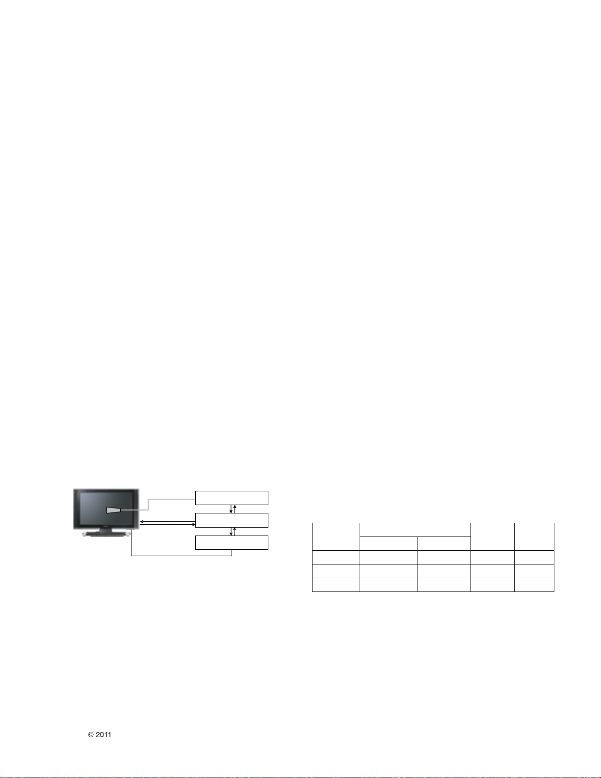
Connecting diagram of equipment for measuring (For
Automatic Adjustment)
1) Set TV in adj. mode using POWER ON key
2) Zero calibrate probe then place it on the center of the
Display
3) Connect Cable(RS-232C)
4) Select mode in adj. Program and begin adj.
5) When adj. is complete (OK Sing), check adj. status pre
mode(Warm, Medium, Cool)
6) Remove probe and RS-232C cable to complete adj.
• W/B Adj. must begin as start command “wb 00 00” , and
finish as end command “wb 00 ff”, and Adj. offset if need
Luminance min value is 150cd in the Cool/Medium/Warm
mode( For LCD)
5.2.2. Adjustment of White Balance (for Manual adjustment)
• Color analyzer(CA100+, CA210) should be used in the
calibrated ch by CS-1000
• Operate the zero-calibration of the CA100+ or CA-210,
then stick sensor to the module when adjusting.
• For manual adjustment, it is also possible by the
following sequence.
1) Select white pattern of heat-run by pressing “POWER
ON” key on remote control for adjustment then operate
heat run longer than 15 minutes.
(If not executed this step, the condition for W/B may be
different.)
2) Push “Exit” key.
3) Change to the AV mode by remote control.
4) Input external pattern (85% white pattern)
5) Push the ADJ key -> Enter “0000” (Password)
6) Select “3. W/B ADJUST”
7) Enter the W/B ADJUST Mode
8) Stick the sensor to the center of the screen and select
each items (Red/Green/Blue Gain and Offset) using
D/ E(CH +/-) key on R/C..
9) Adjust R/ G/ B Gain using F/G(VOL +/-) key on R/C.
10) Adjust three modes all (Cool / Medium / Warm) : Fix
the one of R/G/B gain and change the others
11) When adjustment is completed, Enter “COPY ALL”
12) Exit adjustment mode using EXIT key on R/C.
* CASE
First adjust the coordinate far away from the target
value(x, y).
1. x, y > target
i) Decrease the R, G.
2. x, y < target
i) First decrease the B gain,
ii) Decrease the one of the others.
3. x > target , y < target
i) First decrease B, so make y a little more than the
target.
ii) Adjust x value by decreasing the R
4. x < target , y > target
i) First decrease B, so make x a little more than the
target.
ii) Adjust x value by decreasing the G
• Standard color coordinate and temperature when using
the CA100+ or CA210 equipment
change reason : When vivid mode, more detail than other
company set.
In case of Edge LED module, the color coordinates is
changing by aging, so you have to use the below table.
Colo r Analyzer
Comp ut er
Pattern Ge n e r ator
RS-232C
RS-232C
RS-232C
Probe
Signal Source
* If TV internal pattern is used, not needed
Mode Color Coordination Temp ∆UV
xy
COOL 0.269±0.002 0.273±0.002 13000K 0.0000
MEDIUM 0.285±0.002 0.293±0.002 9300K 0.0000
WARM 0.313+0.002 0.329±0.002 6500K 0.0000
- 23 -
LGE Internal Use OnlyCopyright LG Electronics. Inc. All right reserved.
Only for training and service purposes
The Time Table of color coordinates by SET Aging Time
1) Edge LED Models : LV3700 / LV5500 / LW5700
2) ALEF & IOP model : LW9500 / LW7700/LZ9700
• In the SET applied LED module
(LV55/LW57/LW77/LW95/LZ97 Series), cause of the
physical characteristics of LED Module, sets are taken a
120 minutes by aging time to stabilize a color coordinates.
So White Balance Control equipments have to get the SET
Aging Time from the SET and then going to control the
W/B by revise color coordinates at each time
- To check the Coordinates of White Balance, you have to
measure at the below conditions.
Picture Mode : select Vivid and change
Dynamic Contrast : Off ,
Dynamic Colour : Off,
Clear White : Off
=> Picture Mode change : Vidid => Vivid(User)
(If you miss the upper condition, the coordinates of W/B
can be lower than the spec.)
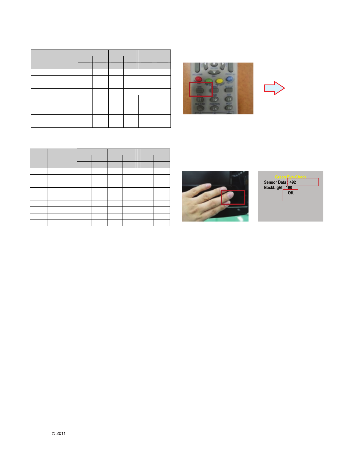
5.3. Intelligent Sensor Inspection Guide
Step 1. Turn on the TV set.
Step 2. Press “EYE” button on the Adjustment remote
controller.
Step 3. Block the Intelligent Sensor module on the front C/A
about 6 seconds.
When the “Sensor Data” is lower than 20, you can see the
“OK” message
=> If it doesn’t show “OK” message, the Sensor Module is
defected one.
You have to replace that with a good one.
Step 4. After check the “OK” message come out, take out
your hand from the Sensor module.
=> Check “Sensor Data” value change from “0” to “300” or
not.
If it doesn’t change the value, the sensor is also defected one.
You have to replace it.
5 20 ~ 35 274 330
6 36 ~ 49 272 327
7 50 ~ 79 271 325
8 80 ~ 149 270 324
9 Over 150 269 323
Cool Medium Warm
x y x y x y
GP3
Aging time
(Min)
269 273 285 293 313 329
1 0 ~ 2 279 338
2 3 ~ 5 278 336
3 6 ~ 9 277 335
4 10 ~19 276
280
277
275
275
263
288
286
285
283
290
288
287
286
285
295
294
293
292
300
297
295
294
293
308
306
305
303
314
312
311
310
309
319
318
317
316 333
Cool Medium Warm
x y x y x Y
GP3
Aging time
(Min)
269 273 285 293 313 329
1 0 ~ 2 282 343
2 3 ~ 5 281 341
3 6 ~ 9 280 340
4 10 ~19 279 338
5 20 ~ 35 277 333
6 36 ~ 49 274 328
7 50 ~ 79 271 326
8 80 ~ 149 270 323
9 Over 150 269
294
292
291
289
284
279
277
274
273
298
297
296
295
293
290
287
286
285
314
312
311
309
304
299
297
294
293
322
321
320
319
317
314
311
310
309 322
- 24 -
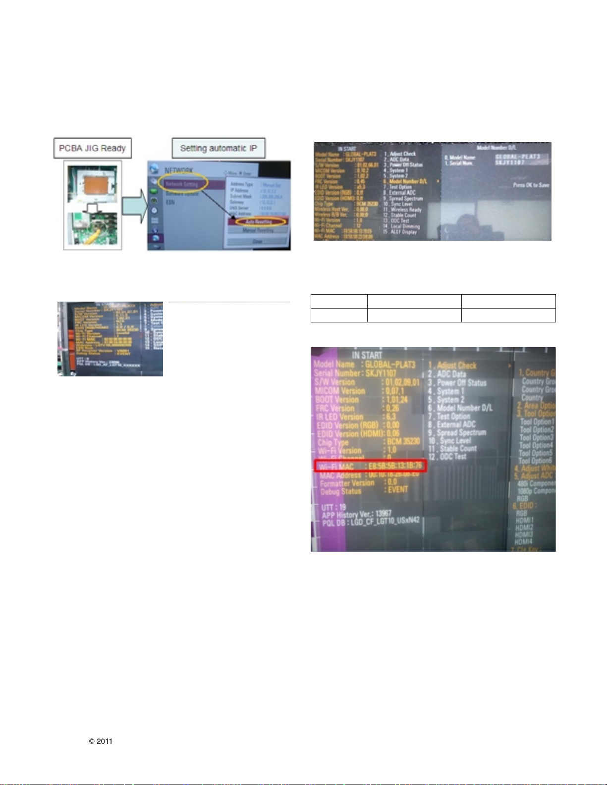
5.4. LAN Inspection
1) LAN Port connection with PCB
2) Network setting at MENU Mode of TV
3) Setting automatic IP
4) Setting state confirmation
5) If automatic setting is finished, you confirm IP and MAC
Address
5.5. WIDEVINE Key Inspection
1) Confirm Key input Data at the “IN START” MENU Mode
5.6. Model name & Serial number D/L
5.6.1. Notice
1) Serial number D/L is using of scan equipment.
2) Setting of scan equipment operated by Manufacturing
Technology Group.
3) Serial number D/L must be conformed when it is produced
in production line, because serial number D/L is mandatory
by D-book 4.0
4) Check the model name In-start menu Factory name
displayed (ex 42LV5500-DD)
5) Check the Diagnostics (DTV country only)-> Buyer model
displayed (ex 42LV5500-DD)
5.6.2. Method : Auto
1) Press “Power on” key of service remocon.(Baud rate :
115200 bps)
2) Connect RS232 Signal Cable to RS-232 Jack
3) Write Serial number by use RS-232.
4) Must check the serial number at Instart menu.
5.6.3. Method : Manual
* If the TV set is downloaded By OTA or Service man,
Sometimes model name or serial number is initialized.
(Not always) It is impossible to download by bar code scan, so
It need Manual download.
1) Press the ‘instart’ key of ADJ remote controller.
2) Go to the menu ‘6.Model Number D/L’ like below photo.
3) Input the Factory model name or Serial number like photo.
5.7. Wi-Fi MAC ADDRESS CHECK
1) Using RS232
2) Check the menu on in-start
LGE Internal Use OnlyCopyright LG Electronics. Inc. All right reserved.
Only for training and service purposes
Command Set ACK
transmission [A][l][][Set ID][][20][Cr] [O][K][x] or [N][G]
- 25 -
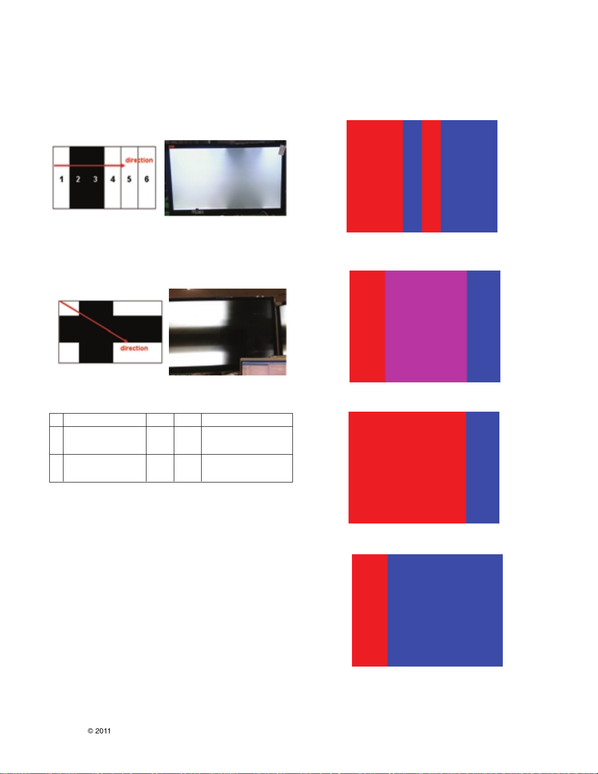
5.8. Local Dimming Inspection (Optional :
over 42”)
5.8.1. Edge LED models with local dimming
1) Press ‘TILT” key of the Adj. R/C and check moving
patterns. The black bar patterns moves from left to right. If
local dimming function does not work, a whole screen
shows full white.
5.6.2. IOP LED models with local dimming
1) Press ‘TILT” key of the Adj. R/C and check moving
patterns. The black cross-bar patterns moves from top-left
to Bottom-right. If local dimming function does not work, a
whole screen shows full white.
5.9. Internal press test
5.10. Motion Remote controller Inspection
5.10.1. Equipment : Motion remote controller for test, IR-KEY-
CODE remote controller for test Check battery before
test. (Recommend : Change battery for every Lot.)
5.10.2. Process
1) Push “Mute” or “ START” key for pairing between TV-set
and motion remote controller.
2) Push “OK” or “Enter” key, you can see the Cursor on
screen.
3) Push “Vol+” or “STOP” key, Disconnect Pairing.
5.11. 3D Function test
5.11.1. Equipment : Pattern Generator MSPG-3233, HDMI
mode 37, pattern No. 81
5.11.2. Process
1) Connect HDMI (HDMI mode 371, Pattern No. 81)
2) Insert 3D Mode, Select side by side mode.
3) Without 3D-glasses, Like below figure.
4) With 3D left-glass, Like below figure. (Center is RED)
5) With 3Dright-glass, Like below figure.(Center is Blue)
LGE Internal Use OnlyCopyright LG Electronics. Inc. All right reserved.
Only for training and service purposes
No Item Vallue Unit Remark
1.
Dielectric Voltage(AC<->FG)
1.5 kV At 100mA for 1sec(Line)
1.5 At 100mA for 1min(OQC)
2.
Dielectric Voltage(Without FG)
3 kV At 100mA for 1sec(Line)
3 At 100mA for 1min(OQC)
- 26 -
LGE Internal Use OnlyCopyright LG Electronics. Inc. All right reserved.
Only for training and service purposes
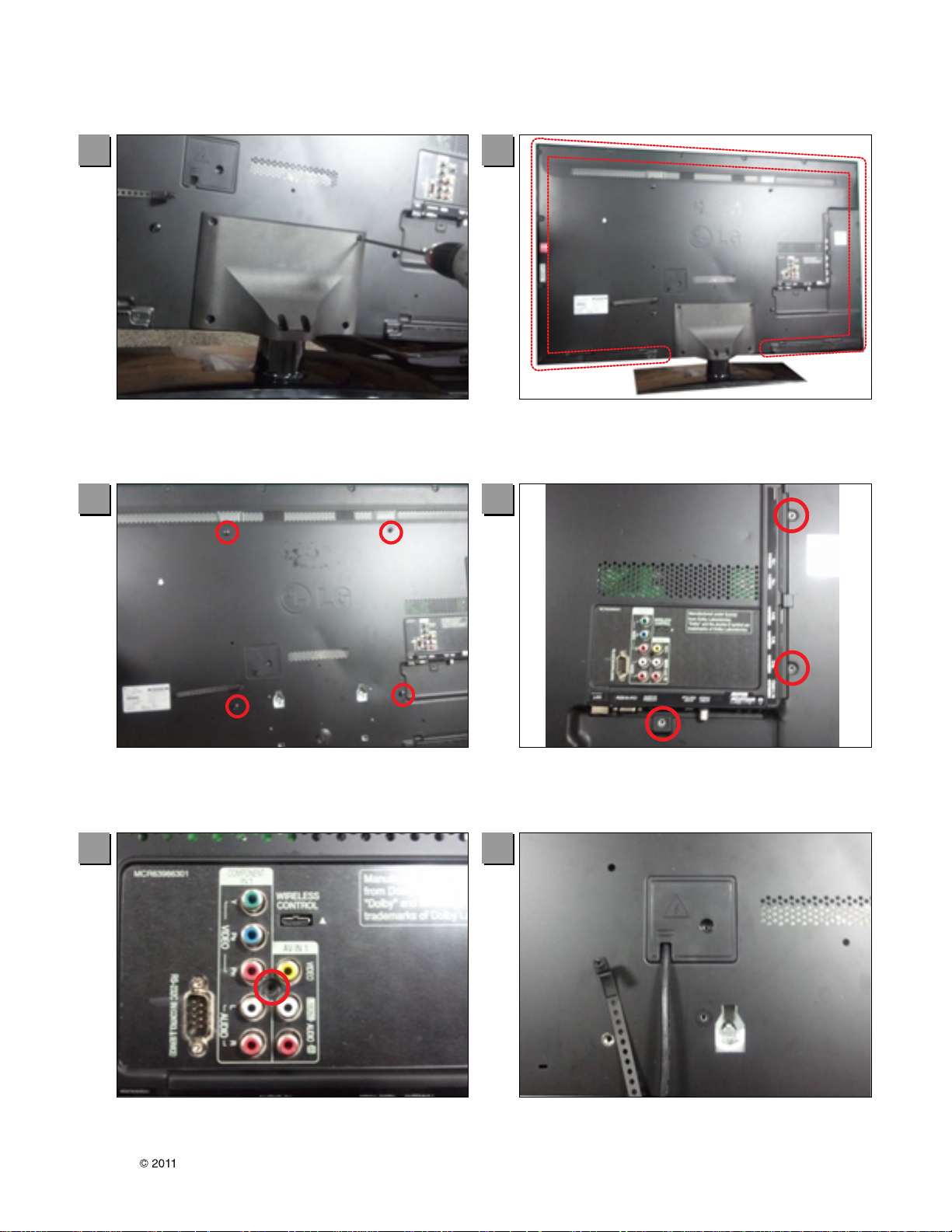
DISASSEMBLY
1 2
Loosen 4 screws that bind Stand Ass’y and set. Disassemble 18 screws around the 4 edges of set after
separation Stand Ass’y.
3 4
Disassemble 4 VESA screws. Disassemble 3 screws that fix Side AV bracket and
Baccover.
5 6
Disassemble 1 screw which bind Main Board and
Backcover.
Detach Power cord Cover from the Backcover.
- 27 -
LGE Internal Use OnlyCopyright LG Electronics. Inc. All right reserved.
Only for training and service purposes
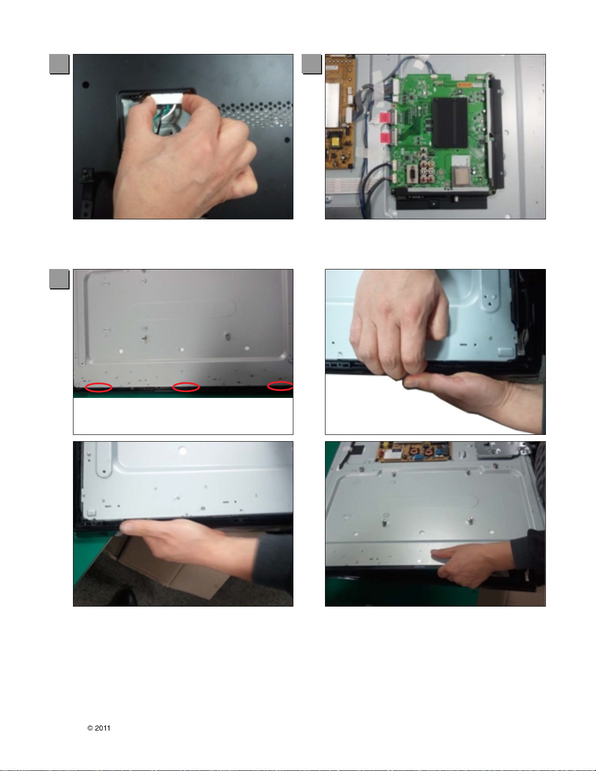
7 8
Push the latch to get Power cord out of the set.
Remove the Backcover.
Push the Panel aside and bend Cabinet back. Take the Panel out of Cabinet by detaching latch.
Disconnect cables of Soft touch PCB, Motion PCB, Speaker
from Main PCB.
9

400
EXPLODED VIEW
IMPORTANT SAFETY NOTICE
Many electrical and mechanical parts in this chassis have special safety-related characteristics. These
parts are identified by in the Schematic Diagram and EXPLODED VIEW.
It is esse ntia l that t hese speci al safety parts shoul d be repla ced with the same compo nent s as
recommended in this manual to prevent X-RADIATION, Shock, Fire, or other Hazards.
Do not modify the original design without permission of manufacturer.
710
A10
LV2
LV1
200
521
540
530
A5
A2
810
900
120
300
Only for training and service purposes
- 28 -
512
511
510
LGE Internal Use OnlyCopyright LG Electronics. Inc. All right reserved.
NAND FLASH MEMORY 8Gbit
+3.3V_Normal
NC_1
1
NC_2
2
NC_3
3
NC_4
4
NC_5
5
NC_6
6
RY/BY
7
RE
8
CE
9
NC_7
10
NC_8
11
VCC_1
12
VSS_1
13
NC_9
14
NC_10
15
CLE
16
ALE
17
WE
18
WP
19
NC_11
20
NC_12
21
NC_13
22
NC_14
23
NC_15
24
LGE35230(BCM35230KFSBG)
B5
C5
A4
B4
A3
B3
A2
B2
W2
V4
W4
V3
V2
D13
E6
R106
3K
IC101
NON_BCM_CAP
HDMI0_CLKN
HDMI0_CLKP
HDMI0_D0N
HDMI0_D0P
HDMI0_D1N
HDMI0_D1P
HDMI0_D2N
HDMI0_D2P
CEC
DDC0_SCL
DDC0_SDA
HDMI0_HTPLG_IN
HDMI0_HTPLG_OUT
HDMI0_ARC
HDMI0_RESREF
LT0VCAL_MONITOR
NAND_RBb
NAND_REb
NAND_CEb
NAND_CEb2
NAND_CLE
NAND_ALE
FLASH_WP
R105
4.7K
NAND_WEb
R104
4.7K
R195
4.7K
Write Protection
- High : Normal Operation
- Low : Write Protection
+3.3V_Normal
R101
4.7K
R107 2.7K
R148
+3.3V_Normal
R103
4.7K
HDMI_CLKHDMI_CLK+
HDMI_RX0HDMI_RX0+
HDMI_RX1HDMI_RX1+
HDMI_RX2HDMI_RX2+
HDMI_ARC
16Gbit
R149 0
16Gbit
0
C102
4700pF
C101
0.1uF
OPT
IC102
TC58DVG3S0ETA00
NAND_8Gbit
TXOUT0_L0N
TXOUT0_L0P
TXOUT0_L1N
TXOUT0_L1P
TXOUT0_L2N
TXOUT0_L2P
TXCLK_LN
TXCLK_LP
TXOUT0_L3N
TXOUT0_L3P
TXOUT0_L4N
TXOUT0_L4P
TXOUT0_U0N
TXOUT0_U0P
TXOUT0_U1N
TXOUT0_U1P
TXOUT0_U2N
TXOUT0_U2P
TXCLK_UN
TXCLK_UP
TXOUT0_U3N
TXOUT0_U3P
TXOUT0_U4N
TXOUT0_U4P
TXOUT1_L0N
TXOUT1_L0P
TXOUT1_L1N
TXOUT1_L1P
TXOUT1_L2N
TXOUT1_L2P
TXCLK1_LN
TXCLK1_LP
TXOUT1_L3N
TXOUT1_L3P
TXOUT1_L4N
TXOUT1_L4P
TXOUT1_U0N
TXOUT1_U0P
TXOUT1_U1N
TXOUT1_U1P
TXOUT1_U2N
TXOUT1_U2P
TXCLK1_UN
TXCLK1_UP
TXOUT1_U3N
TXOUT1_U3P
TXOUT1_U4N
TXOUT1_U4P
GPIO_BL_ON
BL_PWM/GPIO
AE27
AE28
AF27
AF28
AG27
AG28
AE26
AF26
AH27
AG26
AF25
AE25
AH26
AG25
AE24
AD24
AH25
AF24
AE23
AD23
AG24
AF23
AC22
AD22
AG23
AH23
AE22
AE21
AF22
AH22
AG22
AF21
AG21
AF20
AD21
AC21
AG20
AH20
AD19
AE19
AF19
AH19
AE18
AD18
AG19
AF18
AG18
AF17
AC18
AH16
AG16
16Gbit
IC102-*1
TH58DVG4S0ETA20
SDA0_3.3V
SCL0_3.3V
SCL2_3.3V
SDA2_3.3V
R199 22
R197 22
48
47
46
45
44
43
42
41
40
39
38
37
36
35
34
33
32
31
30
29
28
27
26
25
NC_26
NC_25
NC_24
NC_23
I/O8
I/O7
I/O6
I/O5
NC_22
PSL
NC_21
VCC_2
VSS_2
NC_20
NC_19
NC_18
I/O4
I/O3
I/O2
I/O1
NC_17
NC_16
NC_15
NC_14
+3.3V_Normal
NC_1
1
NC_28
48
NC_27
47
NC_26
46
NC_25
45
I/O8
44
NAND_DATA[7]
I/O7
43
NAND_DATA[6]
I/O6
42
NAND_DATA[5]
I/O5
41
NAND_DATA[4]
NC_24
40
39
38
37
36
35
34
33
32
31
30
29
28
27
26
25
PSL
NC_23
VCC_2
VSS_2
NC_22
NC_21
NC_20
I/O4
I/O3
I/O2
I/O1
NC_19
NC_18
NC_17
NC_16
16Gbit
R151
+3.3V_Normal
C104 10uF
NAND_DATA[3]
NAND_DATA[2]
NAND_DATA[1]
NAND_DATA[0]
TXB4P
TXB4N
TXB3P
TXB3N
TXBCLKP
TXBCLKN
TXB2P
TXB2N
TXB1P
TXB1N
TXB0P
TXB0N
TXA4P
TXA4N
TXA3P
TXA3N
TXACLKP
TXACLKN
TXA2P
TXA2N
TXA1P
TXA1N
TXA0P
TXA0N
TXD4P
TXD4N
TXD3P
TXD3N
TXDCLKP
TXDCLKN
TXD2P
TXD2N
TXD1P
TXD1N
TXD0P
TXD0N
TXC4P
TXC4N
TXC3P
TXC3N
TXCCLKP
TXCCLKN
TXC2P
TXC2N
TXC1P
TXC1N
TXC0P
TXC0N
+3.3V_Normal
0
C103
0.1uF
10V
R194
2.7K
R108 10K
NAND_DATA[0-7]
RGB_DDC_SDA
RGB_DDC_SCL
BBS CONNECT
P101
TJC2508-4A
1
2
3
4
C105
2.2uF
10V
Q101
BSS83
Q102
BSS83
+3.3V_Normal
VCC
SCL
SDA
GND
A_DIM
RY/BY2
RY/BY1
VCC_1
VSS_1
NC_10
NC_11
NC_12
NC_13
SBD
G
SBD
G
NC_2
NC_3
NC_4
NC_5
NC_6
NC_7
NC_8
NC_9
CE1
CE2
CLE
ALE
RE
WE
WP
C106
4.7uF
DEV_NAND_16Gbit
2
3
4
5
6
7
8
9
10
11
12
13
14
15
16
17
18
19
20
21
22
23
24
+3.3V_Normal
R196
10K
C118
0.1uF
16V
+3.3V_Normal
R198
10K
C119
0.1uF
16V
R110
R109
1.5K
1.5K
DVB_S Option: apply EU Satellite model
FOR HDMI STANDARD
APPLY ONLY WHEN CONNECT TO PULL-UP GPIO
Boot ROM Device Select - (FA4,FAD7,FAD2,FAD1)
+3.3V_Normal
R113
10K
R114
10K
OPT
R117
10K
OPT
R118
10K
R122
10K
R123
10K
OPT
R127
10K
OPT
R128
10K
CI_ADDR[4]
NAND_DATA[7]
NAND_DATA[2]
NAND_DATA[1]
NAND ECC (FA3, FA2, FALE)
+3.3V_Normal
R119
R115
R111
10K
OPT
R112
10K
10K
R116
10K
OPT
10K
OPT
R120
10K
CI_ADDR[3]
CI_ADDR[2]
NAND_ALE
DUAL COMPONENT
IC102 1ST : EAN61000101 2ND : T-TH58DVG4S0ETA20
IC102-*1
LGE35230(BCM35230KFSBG)
AG6
TVM_XTALIN
AF6
TVM_XTALOUT
V5
IRRXDA
AB4
FP_IN0
Y4
FP_IN1
AA4
SPARE_ADC1
Y5
SPARE_ADC2
AB2
FS_IN1
AB5
FS_IN2
U3
VGA_SDA
U2
VGA_SCL
Y2
RDA
Y1
TDA
33
AA3
BSCDATAA
AA2
BSCCLKA
H3
RDB/GPIO
H2
TDB/GPIO
H4
BSC_S_SCL
H5
BSC_S_SDA
F25
NMIB
W5
POWER_CTRL
U5
AON_HSYNC
U4
AON_VSYNC
W3
AON_GPIO_36
W1
AON_GPIO_37
AB6
AON_RESETOUTB
Y6
TVM_BYPASS
Y3
RESETB
G24
RESETOUTB
J6
TMODE
W6
TESTEN
F7
VDAC_VREG
E7
VDAC_RBIAS
BCM REFRENCE is 562ohm
R121
1.2K
C107
33pF
50V
DVB_S
+3.3V_Normal
+3.3V_Normal
R124
1K
OPT
R125
1K
R126
1.2K
C108
33pF
50V
DVB_S
R129
1.2K
C109
33pF
50V
5V_HDMI_3
R130
OPT
2K
R132 4.7K
+3.3V_Normal
C111 0.01uF
C112 0.1uF
54MHz_XTAL_P
54MHz_XTAL_N
R131
1.2K
C110
33pF
50V
PCM_5V_CTL
5V_HDMI_1
5V_HDMI_2
5V_HDMI_4
SOC_RESET
LNB_INT
SC_ID
BCM_RX
BCM_TX
R135
R136 33
+3.3V_Normal
R141 4.7K
R142 22
R143 22
R144 22
R145 22
R139 0
SRST
R140
560
1%
OPT
OPT
OPT
OPT
0000: ST Micro M25P or compatible Serial Flash
0010: 8-bit 512Mbit 512B page SLC NAND Flash devices
0100: 8-bit 128, 256Mbit 512B page SLC NAND Flash devices
0110: 8-bit 1Gbit 2KB page SLC NAND Flash devices
1000: 8-bit 2Gbit, 4Gbit, 8Gbit 2KB page SLC NAND Flash devices
1010: 8-bit 16Gbit, 32Gbit 4KB page SLC NAND Flash devices (O)
0001: 8-bit 8/16/32Gbit 2KB page MLC NAND Flash devices
0011: 8-bit 16/32Gbit 4KB page MLC NAND Flash devices
0101: 8-bit 32Gbit 8KB page MLC NAND Flash devices
0111: 3B dual IO Serial Flash
1001: BB dual IO Serial Flash
1011: fast Serail Flash > 50Mhz
1100: OneNAND Flash (always 16-bit)
1110: Reserved
1101, 1111: Reserved
000 = ECC disabled
001 = ECC 1-bit repair
010 = ECC 4-bit BCH (O)
011 = ECC 8-bit BCH, 27 byte spare
100 = ECC 12-bit BCH, 27 byte spare
101 = ECC 8-bit BCH, 16 byte spare
110, 111 = Reservedd
IC101
NON_BCM_CAP
AVS_NDRIVE_1
AVS_PDRIVE_1
FAD_7
FAD_6
FAD_5
FAD_4
FAD_3
FAD_2
FAD_1
FAD_0
FALE
FCEB_0
FCEB_1
FCEB_2
FCEB_3
NFWPB
FRDYB
FA_0
FA_1
FA_2
FA_3
FA_4
FA_5
FA_6
FA_7
FA_8
FA_9
FA_10
FA_11
FA_12
FA_13
FA_14
FA_15
TRSTB
TDI/GPIO
TMS/GPIO
TCK/GPIO
DINT/GPIO
AVS_VFB
AVS_VSENSE
AVS_RESETB
VDAC_1
VDAC_2
AB1
NAND_DATA[7]
AB3
NAND_DATA[6]
AC1
NAND_DATA[5]
AC2
NAND_DATA[4]
AC3
NAND_DATA[3]
AD2
NAND_DATA[2]
AD3
NAND_DATA[1]
AE2
NAND_DATA[0]
AG1
AF1
AC5
AE6
AG5
AF3
AG2
FWE
AE3
FRD
AA5
AF2
AE1
AC4
AD5
AD4
AE4
AE5
AD6
AH3
AF4
AH4
AG4
AF5
AG3
AH2
AH5
AD15
AF14
AH14
TDO
AD14
AG14
AC16
AH7
AG7
AD7
AF7
AH8
C6
D7
NAND_ALE
NAND_CEb
NAND_CEb2
/CI_CE1
/CI_CE2
FLASH_WP
NAND_WEb
NAND_REb
/PCM_WAIT
NAND_CLE
NAND_RBb
CI_ADDR[2]
CI_ADDR[3]
CI_ADDR[4]
CI_ADDR[5]
CI_ADDR[6]
CI_ADDR[7]
CI_ADDR[8]
CI_ADDR[9]
CI_ADDR[10]
CI_ADDR[11]
CI_ADDR[12]
CI_ADDR[13]
CI_ADDR[14]
R146 10K
NAND_DATA[0-7]
R147
1K
DTV/MNT_V_OUT
Strap Setting
CI_ADDR[2-14]
+3.3V_Normal
R156
R153
R150
1K
1K
1K
For L/R sync GPIO
SRST
+3.3V_Normal
R166
1K
R157
10K
OPT
R158
10K
R160
10K
OPT
R161
10K
R164
10K
OPT
R165
10K
R154
10K
OPT
R155
10K
NAND_DATA[0]:
0: System is LITTLE endian (O)
1: System is BIG endian
CI_ADDR[7]:
0: Disable EDID automatic Downloading from Flash (O)
1: Enable EDID automatic Downloading from Flash
NAND_DATA[6] :
0: Disable OSC clock output on chip Pin (O)
1: Enable OSC clock output on chip pin.
CI_ADDR[6]:
0: Host MIPS run at 500 MHz (O)
1: Host MIPS run at 250 MHz
NAND_CLE:
0: Differential Oscillators TVM not bypassed (O)
1: Differential Oscillators TVM bypassed
NAND_DATA[4]:
0: 27MHz TVM Crystal Frequency
1: 54MHz TVM Crystal Frequency (O)
R162
R159
1K
1K
R163
1K
L/R_SYNC_DINT
L/R_SYNC_DINT
R167
10K
OPT
R168
10K
R175
10K
OPT
R176
10K
R177
10K
R178
10K
OPT
R170
10K
R171
10K
OPT
CI_ADDR[9],CI_ADDR[11],CI_ADDR[12],CI_ADDR[13]
TVM Crystal oscillator bias/gain control
0000: 210uA
0001: 390uA
0010: 570uA
0011: 730uA
0100: 890uA (O)
0111: 1290uA
1000: 1416uA
1111: 2196uA
0101, 0110, 1001, 1010, 1011, 1100, 1101, 1110: Reserved
CI_ADDR[8]:
0: RESETOUTb (in On/Off only) stay asserted until software releases them.
1: Fix amount of delay for de-assertion on RESETOUTb (in On/IOff only)
at end of RESETb pulse (O)
NAND_DATA[3]:
0: MIPS will boot from external flash (O)
1: MIPS will boot from ROM
NAND_DATA[5]:
0: FLASH MODE (O)
1: BSC_SLAVE(BBS) MODE
R179
10K
OPT
R180
10K
R181
10K
OPT
R182
10K
R183
10K
R184
10K
OPT
R187
10K
OPT
R188
10K
NVRAM
+3.3V_Normal
R169
0
R173
R172
4.7K
4.7K
OPT
R174
4.7K
BCM_NVM_1M
IC103
M24M01-HRMN6TP
OPT
NC
1
E1
2
A8’h
E2
3
VSS
4
+3.3V_Normal
VCC
8
WP
7
SCL
6
SDA
5
R190 33
R191 33
54MHz X-TAL
C113
12pF
50V
3
X-TAL_2
4
GND_2
54MHz
X101
CRYSTAL_BCM_Sunny
C114
12pF
EAW58812611
50V
SUNNY ELECTRONICS CORPORATION
2
1
GND_1
X-TAL_1
R185 0
R186 0
R189
1M
OPT
54MHz_XTAL_N
54MHz_XTAL_P
R192
10K
OPT
NAND_DATA[0]
CI_ADDR[7]
NAND_DATA[6]
CI_ADDR[6]
NAND_CLE
NAND_DATA[4]
CI_ADDR[9]
CI_ADDR[11]
CI_ADDR[12]
CI_ADDR[13]
CI_ADDR[8]
NAND_DATA[3]
NAND_DATA[5]
R193
10K
BCM_NVM_256K
IC103-*1
AT24C256C-SSHL-T
A0
1
A1
2
A2
3
GND
4
Write Protection
- Low : Normal Operation
- High : Write Protection
X101-*2
54MHz
X-TAL_1
1
GND_1
2
CRYSTAL_BCM_KDS
EAW58239604
DAISHINKU CORPORATION.
X101-*1
54MHz
X-TAL_1
1
GND_1
2
CRYSTAL_BCM_Lihom
EAW60763703
LIHOM CO., LTD.
VCC
8
WP
7
SCL
6
SDA
5
SCL3_3.3V
SDA3_3.3V
GND_2
4
X-TAL_2
3
GND_2
4
X-TAL_2
3
THE SYMBOL MARK OF THIS SCHEMETIC DIAGRAM INCORPORATES
SPECIAL FEATURES IMPORTANT FOR PROTECTION FROM X-RADIATION.
FILRE AND ELECTRICAL SHOCK HAZARDS, WHEN SERVICING IF IS
ESSENTIAL THAT ONLY MANUFATURES SPECFIED PARTS BE USED FOR
THE CRITICAL COMPONENTS IN THE SYMBOL MARK OF THE SCHEMETIC.
BCM35230
MAIN & NAND FLASH
2010.09.18
1
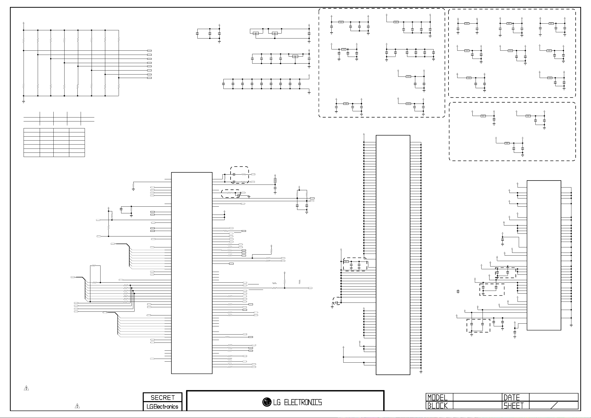
+3.3V_Normal
FHD
R252
1K
HD
R262
1K
PHM
OLED
LCD
BCM
internal
FRC
00 11
1 100
HIGH
Support
FE_TS_DATA[0-7]
CHBO_TS_CLK
CHBO_TS_SERIAL
CHBO_TS_SYNC
CHBO_TS_VAL_ERR
R251
1K
1K
1K
BCM_FRC/URSA5
R261
1K
NO_FRC/FRC2
R250
FRC2/URSA5
R260
NO_FRC/BCM_FRC
MODEL OPTION
MODEL_OPT_0
MODEL_OPT_1
MODEL_OPT_2
MODEL_OPT_3
MODEL_OPT_4
MODEL_OPT_5
MODEL_OPT_6
MODEL_OPT_7 Enable Disable
NO_FRC
DDR speed
T2 Tuner
S Tuner
R253
R263
1K
1K
R254
1K
OPT
R264
1K
LG FRC2
LOW
HDFHD
LCDOLED
16001333
Not Support
Not SupportSupport
R255
1K
T2_TUNER
R265
1K
NO_T2_TUNER
external
URSA5
SIDE_USB_OCD1
SIDE_USB_OCD2
PCM_TS_DATA[0-7]
R201 0
F/NIM_EU_CN
PCM_MDI[0-7]
OPT
R202
0
R256
1K
S_TUNER
R266
1K
NO_S_TUNNER
+3.3V_Normal
R286
10K
WIFI
TU_TS_CLK
FE_TS_DATA[0]
FE_TS_DATA[1]
FE_TS_DATA[2]
FE_TS_DATA[3]
FE_TS_DATA[4]
FE_TS_DATA[5]
FE_TS_DATA[6]
FE_TS_DATA[7]
PHM
NO_PHM
R287
10K
WIFI
R257
1K
R267
1K
R203 0
R204 0
R205 0
R206 0
R207 0
R208 0
R209 0
C201
100pF
OPT
F/NIM_EU_CN
F/NIM_EU_CN
PCM_MDI[0]
PCM_MDI[1]
PCM_MDI[2]
PCM_MDI[3]
PCM_MDI[4]
PCM_MDI[5]
PCM_MDI[6]
PCM_MDI[7]
R211
6.04K
EPHY_TDP
EPHY_TDN
EPHY_RDP
EPHY_RDN
R210
4.87K
1%
SIDE_USB_DM
SIDE_USB_DP
SIDE_USB_CTL1
WIFI_DM
WIFI_DP
SIDE_USB_CTL2
PCM_TS_CLK
PCM_TS_DATA[0]
PCM_TS_DATA[1]
PCM_TS_DATA[2]
PCM_TS_DATA[3]
PCM_TS_DATA[4]
PCM_TS_DATA[5]
PCM_TS_DATA[6]
PCM_TS_DATA[7]
PCM_TS_SYNC
PCM_TS_VAL
F/NIM_EU_CN
F/NIM_EU_CN
F/NIM_EU_CN
F/NIM_EU_CN
F/NIM_EU_CN
TU_TS_SYNC
TS_VAL_ERR
PCM_MCLKI
PCM_MISTRT
PCM_MIVAL_ERR
/PCM_IRQA
MODEL_OPT_0
MODEL_OPT_1
MODEL_OPT_2
MODEL_OPT_3
MODEL_OPT_4
MODEL_OPT_5
MODEL_OPT_6
MODEL_OPT_7
LGE35230(BCM35230KFSBG)
F26
D26
F27
F28
E27
E26
F5
E5
C2
D1
E1
D2
B1
C1
C3
C4
M4
L5
M5
L6
N3
N1
N2
M3
M2
L4
N4
K6
J4
K5
J2
J3
K2
K1
K3
L1
L3
L2
P4
T2
R3
R2
P3
P2
P1
R6
N5
T4
P5
R4
U1
T3
T1
T5
IC101
NON_BCM_CAP
EPHY_VREF
EPHY_RDAC
EPHY_TDP
EPHY_TDN
EPHY_RDP
EPHY_RDN
USB_MONCDR
USB_RREF
USB_PORT1DN
USB_PORT1DP
USB_PWRFLT_1/GPIO
USB_PWRON_1/GPIO
USB_PORT2DN
USB_PORT2DP
USB_PWRFLT_2/GPIO
USB_PWRON_2/GPIO
TCLKA/GPIO
TDATA_0/GPIO
TDATA_1/GPIO
TDATA_2/GPIO
TDATA_3/GPIO
TDATA_4/GPIO
TDATA_5/GPIO
TDATA_6/GPIO
TDATA_7/GPIO
TSTRTA/GPIO
TVLDA/GPIO
TCLKD/GPIO
TDATD_0/GPIO
TDATD_1/GPIO
TDATD_2/GPIO
TDATD_3/GPIO
TDATD_4/GPIO
TDATD_5/GPIO
TDATD_6/GPIO
TDATD_7/GPIO
TSTRTD/GPIO
TVLDD/GPIO
MPEG_CLK/GPIO
MPEG_D_0/GPIO
MPEG_D_1/GPIO
MPEG_D_2/GPIO
MPEG_D_3/GPIO
MPEG_D_4/GPIO
MPEG_D_5/GPIO
MPEG_D_6/GPIO
MPEG_D_7/GPIO
MPEG_SYNC/GPIO
MPEG_DATA_EN/GPIO
MCIF_RESET/GPIO
MCIF_SCLK/GPIO
MCIF_SCTL/GPIO
MCIF_SDI/GPIO
MCIF_SDO/GPIO
PCI_DEVSELB/GPIO
PCI_FRAMEB/GPIO
C225
0.22uF
6.3V
VI_IFP0
VI_IFM0
VDDR_AGC
AGC_SDM_2
AGC_SDM_1
GPIO_0
GPIO_1
GPIO_2
GPIO_3
PCI_VIO_0
PCI_VIO_1
PCI_VIO_2
GPIO_4
GPIO_5
GPIO_6
GPIO_7
GPIO_70
GPIO_71
GPIO_72
GPIO_73
GPIO_74
GPIO_75
GPIO_76
GPIO_77
GPIO_78
GPIO_79
PCI_AD05
PCI_AD06
PCI_AD07
PCI_AD08
PCI_AD09/GPIO
PCI_AD10/GPIO
PCI_AD11/GPIO
PCI_AD12/GPIO
PCI_AD13/GPIO
PCI_AD14/GPIO
PCI_AD15/GPIO
PCI_AD16/GPIO
PCI_AD17/GPIO
PCI_AD18/GPIO
PCI_AD19/GPIO
PCI_AD20/GPIO
PCI_AD21/GPIO
PCI_AD22
PCI_AD23
PCI_AD24
PCI_AD25
PCI_CBE00
PCI_CBE01/GPIO
PCI_CBE02/GPIO
PCI_CBE03
PCI_IRDYB/GPIO
PCI_PAR/GPIO
PCI_PERRB/GPIO
PCI_REQ1B
PCI_SERRB/GPIO
PCI_STOPB/GPIO
PCI_TRDYB/GPIO
+0.9V_CORE
C221
0.1uF
C17
B17
D15
B16
A16
A15
C16
G28
G26
+3.3V_Normal
W14
W15
W13
J5
R5
V6
H6
AE15
AF15
AG15
AF16
AD16
AE16
AG17
AH17
AE17
AD17
AB13
AC15
AB12
AB11
AE14
AG13
AH13
AF13
AE13
AD12
AF12
AG10
AF10
AE10
AD10
AE9
AE8
AC10
AC11
AC8
AB8
AC14
AG12
AH10
AB7
AG11
AD11
AE11
AD13
AE12
AC12
AC13
AH11
AF11
C223
0.01uF
C203
10uF
10V
close to soc
Non_CHB
R212
1K
closed to soc
R213 2K
C216 0.01uF
R280
22
R214 22
R215 22
R281 22
R282 22
R216 22
R218 22
R220 22
R221 22
R222 22
R283
22
R223 22
R284 22
R224 22
R235
R225 0
R226 22
R285 22
R227 22
C207
C205
4.7uF
10uF
10V
10V
C217
16V
100
0.1uF
R241
C218
100
0.1uF
R242
16V
M_REMOTE_RX
CI_DET
M_RFModule_RESET
EPHY_ACTIVITY
EPHY_LINK
DTV_ATV_SELECT
RF_SWITCH_CTL_2
INSTANT_MODE
BCM_L/DIM
BCM_L/DIM
100
OPT
NFM18PS105R0J
C233
6.3V
GND
C232
4.7uF
10V
C209
4.7uF
10V
IF_P
IF_N
IF_AGC
3D_SYNC
MODEL_OPT_0
MODEL_OPT_1
MODEL_OPT_2
MODEL_OPT_3
SC_DET/COMP2_DET
CHB_RESET
TW9910_RESET
AV2_CVBS_DET
RF_BOOSTER_CTL
DSUB_DET
PCM_RST
MODEL_OPT_4
DC_MREMOTE
DD_MREMOTE
L/DIM0_MOSI
L/DIM0_SCLK
COMP1_DET
MODEL_OPT_5
3D_GPIO_0
MODEL_OPT_6
MODEL_OPT_7
ERROR_OUT
RF_SWITCH_CTL
3D_GPIO_1
3D_GPIO_2
OUTIN
C234
0.1uF
C211
0.1uF
+3.3V_Normal
R228 22
R230 22
BCM_L/DIM
NFM18PS105R0J
C204
6.3V
GND
C236
0.1uF
C213
0.1uF
+3.3V_Normal
BLM18PG121SN1D
0.1uF
R240
2.7K
+3.3V_Normal
R231-*1 0
FRC2_RESET
R231 100
URSA_RESET
OUTIN
NFM18PS105R0J
C238
4.7uF
10V
C215
0.01uF
L201
C229
C244
6.3V
C220
0.1uF
+3.3V_Normal
NON_NTP
PWM_DIM
L/DIM0_VS
R232
4.7K
URSA_RESET
GND
R232-*1
4.7K
OUTIN
R233
1.2K
C227
33pF
50V
+0.9V_CORE
C247
22uF
+3.3V_Normal
C248
10uF
10V
+1.5V_DDR
C222
0.01uF
R234
1.2K
C231
33pF
50V
FRC2_RESET
POWER 2.5V
+2.5V_BCM35230
+2.5V_BCM35230
+2.5V_BCM35230
SDA1_3.3V
SCL1_3.3V
NON_NTP
FRC_RESET
Place Cap
Very close to R22 Ball
L202
BLM18PG121SN1D
C249
10uF
10V
L203
BLM18PG121SN1D
C251
0.1uF
16V
L204
BLM18PG121SN1D
C250
4.7uF
10V
+1.5V_DDR
Place Cap
Very close to R22 Ball
C242
0.1uF
+3.3V_Normal
C253
10uF
10V
EPHY_VDD25
C252
4.7uF
10V
VAFE3_VDD25
C254
4.7uF
MLG1005S22NJT
C224
L220
1uF
25V
OPT
+0.9V_CORE
AADC_AVDD25
C256
0.1uF
C255
0.1uF
C257
0.1uF
+0.9V_CORE
C226
0.1uF
16V
OPT
+3.3V_Normal
+2.5V_BCM35230
L205
BLM18PG121SN1D
C258
0.1uF
+2.5V_BCM35230
C260
C259
4.7uF
10uF
10V
+2.5V_BCM35230
+2.5V_BCM35230
NON_BCM_CAP
VDDC_1
VDDC_2
VDDC_3
VDDC_4
VDDC_5
VDDC_6
VDDC_7
VDDC_8
VDDC_9
VDDC_10
VDDC_11
VDDC_12
VDDC_13
VDDC_14
VDDC_15
VDDC_16
VDDC_17
VDDC_18
VDDC_19
VDDC_20
VDDC_21
VDDC_22
VDDC_23
VDDC_24
VDDC_25
VDDC_26
VDDC_27
VDDC_28
VDDC_29
VDDC_30
VDDC_31
VDDC_32
VDDC_33
VDDC_34
VDDC_35
VDDC_36
VDDC_37
VDDC_38
VDDC_39
VDDC_40
VDDC_41
VDDC_42
POR_VDD
VDDR1_1
VDDR1_2
VDDR1_3
VDDR1_4
VDDR1_5
VDDR1_6
VDDR1_7
VDDR1_8
VDDR1_9
VDDR1_10
VDDR1_11
VDDR1_12
DDR_LDO_VDDO
VDDR3_1
VDDR3_2
VDDR3_3
VDDR3_4
VDDR3_5
VDDR3_6
VDDR3_7
VDDR3_8
VDDR3_9
VDDR3_10
VDDR3_11
AON_VDDC_1
AON_VDDC_2
AON_POR_VDD
AON_VDDR3
AON_VDDR10_1
AON_VDDR10_2
IC101
LGE35230(BCM35230KFSBG)
V12
V7
M10
N10
P10
R10
T10
U10
V10
W10
V13
L11
M11
N11
P11
R11
T11
U11
V11
W11
V14
L18
M18
N18
P18
R18
T18
U18
V18
W18
V15
L19
M19
N19
P19
R19
T19
U19
V19
W19
V16
V17
L10
L22
AA28
V28
R28
M28
J28
K23
M22
T22
T23
U22
Y22
R22
G15
H22
G23
AB9
K7
AB15
L7
AB14
M7
N6
P6
AA6
AA7
Y7
U7
T7
T6
C261
10uF
10V
C262
10uF
L206
BLM18PG121SN1D
L207
BLM18PG121SN1D
K10
VSS_1
K11
VSS_2
K12
VSS_3
L12
VSS_4
M12
VSS_5
N12
VSS_6
P12
VSS_7
R12
VSS_8
T12
VSS_9
U12
VSS_10
W12
VSS_11
K13
VSS_12
L13
VSS_13
M13
VSS_14
N13
VSS_15
P13
VSS_16
R13
VSS_17
T13
VSS_18
U13
VSS_19
W16
VSS_20
K14
VSS_21
L14
VSS_22
M14
VSS_23
N14
VSS_24
P14
VSS_25
R14
VSS_26
T14
VSS_27
U14
VSS_28
K15
VSS_29
L15
VSS_30
M15
VSS_31
N15
VSS_32
P15
VSS_33
R15
VSS_34
T15
VSS_35
U15
VSS_36
K16
VSS_37
L16
VSS_38
M16
VSS_39
N16
VSS_40
P16
VSS_41
R16
VSS_42
T16
VSS_43
U16
VSS_44
K17
VSS_45
L17
VSS_46
M17
VSS_47
N17
VSS_48
P17
VSS_49
R17
VSS_50
T17
VSS_51
U17
VSS_52
W17
VSS_53
K18
VSS_54
K19
VSS_55
H7
VSS_56
G14
VSS_57
AB16
VSS_58
R7
VSS_59
M6
VSS_60
AB23
VSS_61
P7
VSS_62
W7
VSS_63
J7
VSS_64
N7
VSS_65
AB10
VSS_66
AC23
VSS_67
AC6
VSS_68
G19
VSS_69
AA22
VSS_70
J23
VSS_71
J22
VSS_72
K22
VSS_73
J25
VSS_74
N22
VSS_75
N23
VSS_76
M25
VSS_77
P22
VSS_78
R25
VSS_79
V22
VSS_80
W22
VSS_81
W23
VSS_82
V25
VSS_83
AA25
VSS_84
ADAC_AVDD25
C263
4.7uF
C265
4.7uF
PLL_VAFE_AVDD25
C264
4.7uF
C271
C267
0.01uF
0.1uF
C266
C270
0.1uF
C269
0.1uF
C268
0.1uF
C272
0.01uF
4.7uF C277
VAFE2_VDD25
CORE 0.9V
+0.9V_CORE
L209
BLM18PG121SN1D
C274
22uF
+0.9V_CORE
L210
BLM18PG121SN1D
+0.9V_CORE
L211
BLM18PG121SN1D
POWER 3.3V
+3.3V_Normal
Place as close as possible to the pad
use only for A0/B0 chip
C210-*1
220pF
50V
BCM_A0/B0
PLL_VAFE_AVDD25
+0.9V_CORE
Place as close as possible to the pad
C281
0.1uF
C282
0.1uF
L212
VAFE2_DVDD
VAFE3_DVDD
C208
390pF
50V
C206
390pF
50V
+0.9V_CORE
+0.9V_CORE
USB_AVDD33
C283
0.1uF
+3.3V_Normal
+2.5V_BCM35230
+2.5V_BCM35230
VDAC_AVDD33
BCM_C0
PLL_MIPS_AVDD
C273
0.1uF
BLM18PG121SN1D
C284
22uF
BLM18PG121SN1D
L213
BLM18PG121SN1D
ADAC_AVDD25
EPHY_VDD25
HDMI_AVDD33
C275
0.1uF
OPT
USB_AVDD33
C212
390pF
50V
C210
390pF
50V
PLL_MAIN_AVDD
C276
0.01uF
OPT
HDMI_AVDD
C280
0.1uF
PLL_AUD_AVDD
4.7uF
PLL_VAFE_AVDD
C279
4.7uF
BLM18PG121SN1D
VAFE2_VDD25
VAFE3_VDD25
Place as close as possible to the pad
PLL_VAFE_AVDD
C202
390pF
50V
L214
C285
4.7uF
L215
+3.3V_Normal
AADC_AVDD25
HDMI_AVDD
USB_AVDD
C214
390pF
50V
PLL_AUD_AVDD
+3.3V_Normal
C288
0.1uF
C290
0.1uF
L216
BLM18PG121SN1D
C289
0.1uF
+0.9V_CORE
+0.9V_CORE
+0.9V_CORE
HDMI_AVDD33
C291
4.7uF
USB_AVDD
VAFE3_DVDD
C287
4.7uF
VDAC_AVDD33
C286
4.7uF
LGE35230(BCM35230KFSBG)
AADC_AVDD25
ADACA_AVDD25
ADACC_AVDD25
ADACD_AVDD25
EPHY_BVDD25
EPHY_AVDD25
D5
HDMI0_AVDD
D4
HDMI0_AVDD33
LT0VDD25_1
LT0VDD25_2
LT0VDD25_3
LT0VDD25_4
SPDIF_IN_AVDD25
E4
USB_AVDD
D3
USB_AVDD33
D6
VDAC_AVDD33
VAFE2_DVDD
VAFE2_AVDD25_1
VAFE2_AVDD25_2
VAFE2_DVDD25
D9
VAFE3_DVDD
D8
VAFE3_AVDD25_1
E8
VAFE3_AVDD25_2
F9
VAFE3_AVDD25_3
E9
VAFE3_DVDD25
F8
POR_VDD25
PLL_AUD_AVDD
K4
PLL_MAIN_AVDD
PLL_MIPS_AVDD
PLL_VAFE_AVDD
PLL_VAFE_AVDD25
TVM_OSC_AVDD
U6
AUX_AVDD33
NON_BCM_CAP
C278
0.1uF
AE20
AD20
AC20
AB20
AD25
F19
D25
D24
E24
F24
E25
D14
D18
E17
D16
D17
G25
D11
D12
AE7
L219
BLM18PG121SN1D
C292
22uF
L217
BLM18PG121SN1D
L218
BLM18PG121SN1D
C293
0.1uF
IC101
AADC_AVSS
ADACA_AVSS
ADACC_AVSS
ADACD_AVSS
EPHY_AVSS
HDMI0_AVSS_1
HDMI0_AVSS_2
LT0VSS_1
LT0VSS_2
LT0VSS_3
LT0VSS_4
LT0VSS_5
LT0VSS_6
LT0VSS_7
SPDIF_IN_AVSS
USB_AVSS_1
USB_AVSS_2
VDAC_AVSS
VAFE2_VSS_1
VAFE2_VSS_2
VAFE2_VSS_3
VAFE2_VSS_4
VAFE2_VSS_5
VAFE2_VSS_6
VAFE2_VSS_7
VAFE3_VSS_1
VAFE3_VSS_2
VAFE3_VSS_3
VAFE3_VSS_4
VAFE3_VSS_5
VAFE3_VSS_6
PLL_MIPS_AVSS
TVM_OSC_AVSS
VAFE2_DVDD
C299
C296
0.1uF
4.7uF
PLL_MAIN_AVDD
C294
C297
4.7uF
0.1uF
PLL_MIPS_AVDD
C295
C298
4.7uF
0.1uF
F20
G22
G21
F22
F23
F6
G6
AB22
AB21
AB19
AC19
AB18
AB17
AC17
F15
G7
G8
G9
G20
E18
G18
G17
F18
G16
F16
G13
G12
F12
G11
G10
F10
AD26
AC7
THE SYMBOL MARK OF THIS SCHEMETIC DIAGRAM INCORPORATES
SPECIAL FEATURES IMPORTANT FOR PROTECTION FROM X-RADIATION.
FILRE AND ELECTRICAL SHOCK HAZARDS, WHEN SERVICING IF IS
ESSENTIAL THAT ONLY MANUFATURES SPECFIED PARTS BE USED FOR
THE CRITICAL COMPONENTS IN THE SYMBOL MARK OF THE SCHEMETIC.
BCM35230
MAIN POWER
2
50
 Loading...