

LG 43LD430EQE Monitor

SPECIFICATION
LD430EQE-FPA1
43" - UHD - V-by-One
Version: 1.0
Date: 20.01.2021
Note: This specification is subject to change without prior notice
www.data-modul.com

( ) Preliminary Specification
( ● ) Final Specification
Title 43.0” QWUXGA TFT LCD
LD430EQE
Product Specification
SPECIFICATION
FOR
APPROVAL
BUYER General
SET MODEL
APPROVED BY
/
/
/
SIGNATURE
DATE
SUPPLIER LG Display Co., Ltd.
*MODEL LD430EQE
SUFFIX FPA1(RoHS Verified)
APPROVED BY
JaeBum Chun / Team Leader
REVIEWED BY
YoungMin Cho / Project Leader
PREPARED BY
Yanggu Kang / Engineer
SIGNATURE
DATE
Please return 1 copy for your confirmation with
your signature and comments.
Ver. 1.0
TV Product Development Dept.
LG Display Co., Ltd.
1 /39
Number
Product Specification
CONTENTS
ITEM
LD430EQE
Page
COVER
CONTENTS
RECORD OF REVISIONS 3
1
2
3
3-1
3-2
3-3
3-4 V by Oone SIGNAL SPECIFICATIONS 11
3-5
3-6
4
5
6
7
GENERAL DESCRIPTION
ABSOLUTE MAXIMUM RATINGS
ELECTRICAL SPECIFICATIONS
ELECTRICAL CHARACTERISTICS
INTERFACE CONNECTIONS
SIGNAL TIMING SPECIFICATIONS
COLOR DATA REFERENCE
POWER SEQUENCE
OPTICAL SPECIFICATIONS
MECHANICAL CHARACTERISTICS
RELIABILITY
INTERNATIONAL STANDARDS
1
2
4
5
6
6
8
10
13
14
15
19
22
23
7-1
7-2
8 PACKING 24
8-1 INFORMATION OF LCM LABEL 24
8-2 PACKING FORM 24
9
9-1
9-2
9-3 ELECTROSTATIC DISCHARGE CONTROL 26
9-4 PRECAUTIONS FOR STRONG LIGHT EXPOSURE 26
9-5 STORAGE 26
9-6 HANDLING PRECAUTIONS FOR PROTECTION FILM 26
9-7 Appropriate Condition for Commercial Display
Ver. 1.0
Safety
ENVIRONMENT
PRECAUTIONS
MOUNTING PRECAUTIONS
OPERATING PRECAUTIONS
23
23
25
25
25
27
2 /39
Product Specification
RECORD OF REVISIONS
Revision No. Revision Date Page Description
0.1 Feb, 19, 2020 - Preliminary Specification (First Draft)
0.2 Mar, 10, 2020 8 Updated MODULE CONNECTOR(CN1) PIN CONFIGURATION
0.3 April, 13, 2020 20,21 Updated LCM Dimension
15 Update the color coordinates
0.4 April, 14, 2020 - Changed suffix (FPA3 → FPA2)
0.5 June, 06, 2020
0.6 Aug, 31, 2020 20 Change drawing spec
0.7 Oct, 31, 2020 Table 4. PIN CONFIGURATION
0.9 Nov, 12,2020 15 CR 1100 1000
1.0 Jan, 20, 2021 7 Updated Note 8
19 Updated Table 12
LD430EQE
20 Change drawing spec
34 Updated APPENDIX-V
- Final specification.
Ver. 1.0
3 /39
LD430EQE
Product Specification
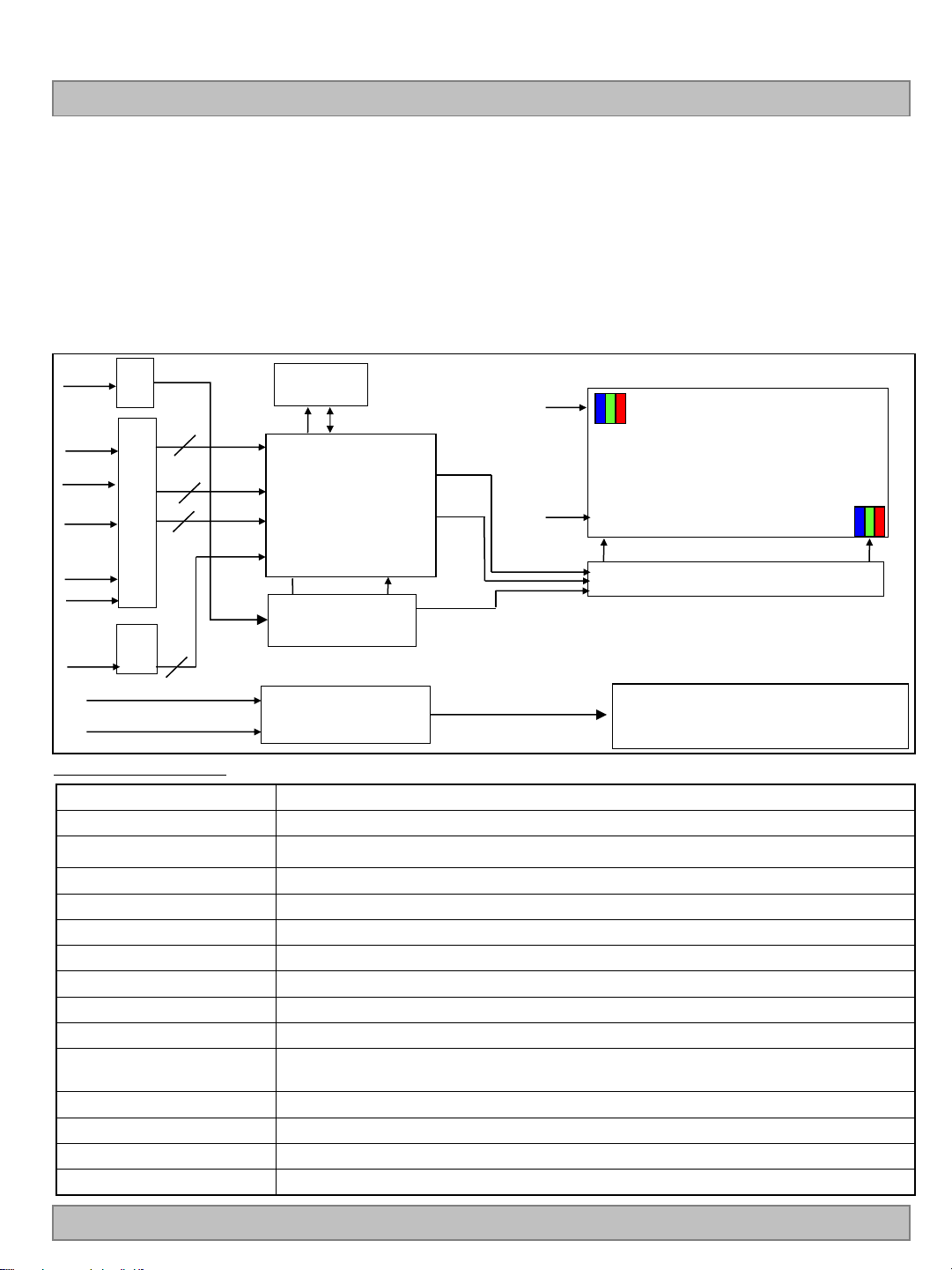
1. General Description
The LD430EQE is a Color Active Matrix Liquid Crystal Display with an integral Light Emitting Diode (LED)
backlight system. The matrix employs a-Si Thin Film Transistor as the active element.
It is a transmissive display type which is operating in the normally black mode. It has a 48.50 inch diagonally
measured active display area with QWUXGA resolution (2160 vertical by 3840 horizontal pixel array).
Each pixel is divided into Red, Green and Blue sub-pixels or dots which are arrayed in vertical stripes.
Gray scale or the luminance of the sub-pixel color is determined with a 10-bit gray scale signal for each dot.
Therefore, it can present a palette of more than 1.07Bilion colors.
It has been designed to apply the 10-bit 8 Lane V by One interface.
It is intended to support LCD TV, PCTV where high brightness, super wide viewing angle, high color gamut,
high color depth and fast response time are important.
CN1
+12.0V
Vby1
8lane
Data
format
Bit
selection
HTPDN
LOCKN
Vby1
8lane
5pin)
CN2
(51pin)
CN3
(41pin)
+12.0V
Vby1
1~8lane
Option
signal
I2C
Vby1
9~16lane
EEPROM
SCL
SDA
Timing Controller
Vby1 Rx
+ DGA + ODC
+L/D
Power Circuit
Block
EPI (RGB)
Control
Signals
Power Signals
G1
G2160
TFT - LCD Panel
(3840 × RGB × 2160 pixels)
S3840
Source Driver Circuit
S1
LED Anode
LED Cathode
CN1 (8pin)
CN2 (8pin)
Back light Assembly
General Features
Active Screen Size 42.51 inches diagonal
Outline Dimension 962.0(H) x 554.8 (V) x 9.6 mm(D)
Pixel Pitch
Pixel Format 3840 horiz. by 2160 vert. Pixels.
Display Mode IPS
Color Depth 10bit(D), 1.07Billon colors
Interface Vby1 8Lane
Luminance, White 700cd/m2 (Center 1point ,Typ.)
BLU Type Edge type
Viewing Angle (CR>10) Viewing angle free ( R/L 178 (Min.), U/D 178 (Min.))
Power Consumption
Weight 8.5Kg (Typ), 9.35Kg(Max)
Display Mode Transmissive mode, Normally black
Surface Treatment Hard coating(2H), Anti-glare treatment of the front polarizer (Haze 28%(Typ.))
Possible Display Type Landscape and Portrait Enabled (counter clock wised)
0.2451 [mm] x 0.2451 [mm]
Total 78.42 W (Typ.)
[Logic= 6.72W (Typ.), BLU=71.7W (IF_cathode=75mA, LED Only)]
Ver. 1.0
4 /39

LD430EQE
Product Specification
2. Absolute Maximum Ratings
The following items are maximum values which, if exceeded, may cause faulty operation or permanent damage
to the LCD module.
Table 1. ABSOLUTE MAXIMUM RATINGS
Parameter Symbol
Unit Note
Min Max
Power Input Voltage LCD Circuit VLCD -0.3 +14.0 VDC
Value
LED Input Voltage Forward Voltage VF - 93.8V VDC
T-Con Option Selection Voltage VLOGIC
Operating Temperature TOP 0 +50
-0.3 +4.0 VDC
°C
1
2
Storage Temperature TST -20 +60
Panel Front Temperature
(Considering L/C Phase Transition Temperature)
TSUR
- +68
°C
°C
3
Operating Ambient Humidity HOP 10 90 %RH
2
Storage Humidity HST 5 90 %RH
Notes
1. Ambient temperature condition (Ta = 25 2 °C )
2. Temperature and relative humidity range are shown in the figure below.
Wet bulb temperature should be Max 39°C, and no condensation of water.
3. Gravity mura can be guaranteed below 50°C and under backlight luminance 700nit condition.
4. The maximum operating temperatures is based on the test condition that the surface temperature
of display area is less than or equal to 68°C with LCD module alone in a temperature controlled chamber.
Thermal management should be considered in final product design to prevent the surface temperature of
display area from being over 68℃. The range of operating temperature may be degraded in case of
improper thermal management in final product design.
5. Prevent products from being exposed to the direct sunlight. Otherwise, its reliability and function may
not be guaranteed
90%
60
60%
Ver. 1.0
Wet Bulb
Temperature [°C]
20
10
0
10 20 30 40 50 60 70 80 0 -20
Dry Bulb Temperature [°C]
30
40
50
40%
10%
5%
Storage
Operation
Humidity [(%)RH]
5 /39
LD430EQE
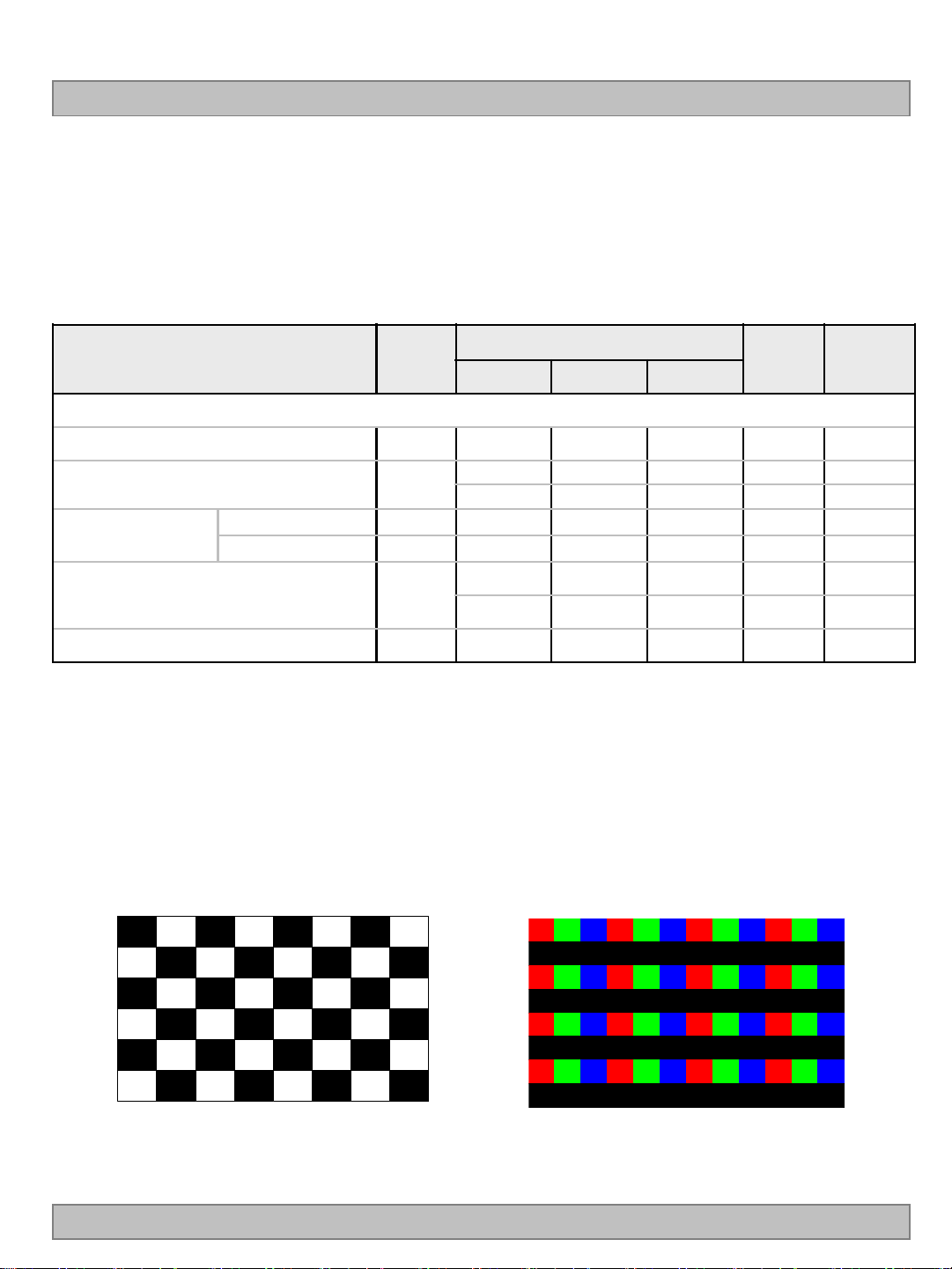
R G B R G B R G B R G B
R G B R G B R G B R G B
R G B R G B R G B R G B
R G B R G B R G B R G B
R G B R G B R G B R G B
R G B R G B R G B R G B
R G B R G B R G B R G B
R G B R G B R G B R G B
Product Specification
3. Electrical Specifications
3-1. Electrical Characteristics
It requires two power inputs. One is employed to power for the LCD circuit. The other Is used for the LED
backlight and LED Driver circuit.
Table 2. ELECTRICAL CHARACTERISTICS
Parameter Symbol
Min Typ Max
Circuit :
Power Input Voltage VLCD 10.8 12.0 13.2 VDC
Power Input Current ILCD
T-CON Option
Selection Voltage
Power Consumption PLCD
Rush current IRUSH - - 10 A 3
Input High Voltage V
Input Low Voltage VIL 0 - 0.7
IH
-
-
2.7 - 3.6
-
-
Value
560 730
1183 1540
6.72 8.74
14.20 18.45
Unit Note
mA 1
mA 2
VDC
VDC
Watt 1
Watt 2
notes
1. The specified current and power consumption are under the V
condition, and mosaic pattern(8 x 6) is displayed and f
is the frame frequency.
V
=12.0V, Ta=25 2°C, fV=60Hz
LCD
2. The current is specified at the maximum current pattern.
3. The duration of rush current is about 2ms and rising time of power input is 0.5ms (min.).
4. Ripple voltage level is recommended under ±5% of typical voltage
White : 1023 Gray
Black : 0 Gray
Ver. 1.0
Mosaic Pattern(8 x 6)
Max Current Pattern
6 /39

Product Specification
LD430EQE
Table 3. ELECTRICAL CHARACTERISTICS (Continue)
Parameter Symbol
Backlight Assembly :
Forward Current
(one array)
Forward Voltage V
Forward Voltage Variation
Power Consumption P
Burst Dimming Duty On duty
Burst Dimming Frequency 1/T
LED Array : (APPENDIX-V)
Life Time 30,000 50,000 Hrs 7
Notes :
The design of the LED driver must have specifications for the LED array in LCD Assembly.
The electrical characteristics of LED driver are based on Constant Current driving type.
Anode I
Cathode I
F (anode)
F (cathode)
F
△V
F
BL
Min Typ Max
- 450 - mAdc
- 75 - mAdc
73.0 79.7 83.8 Vdc
65.7 71.7 75.4 6
1 100 %
95 182 Hz 8
Values
Ta = 25±2℃, On Duty 100%
Unit Note
1.7 Vdc
The performance of the LED in LCM, for example life time or brightness, is extremely influenced by the
characteristics of the LED Driver. So, all the parameters of an LED driver should be carefully designed.
When you design or order the LED driver, please make sure unwanted lighting caused by the mismatch of the
LED and the driver (no lighting, flicker, etc) has never been occurred. When you confirm it, the LCD–
Assembly should be operated in the same condition as installed in your instrument.
1. Electrical characteristics are based on LED Array specification.
2. Specified values are defined for a Backlight Assembly. (IBL :2 LED array/LCM)
Electrical characteristics are determined after the unit has been ‘On’ and stable for approximately 60min at
25±2℃. The specified temperature, optical and power consumption are under the typical supply input voltage,
current & VBR (duty : 100%), it is total power consumption.
3. Each LED array has one anode terminal and six cathode terminals.
The forward current(IF) of the anode terminal is
1string( 9LED PKG)
450mA and it supplies 75mA into an one strings, respectively
Anode#1
Anode#2
450mA
450mA
° ° °
° ° °
° ° °
° ° °
° ° °
° ° °
Cathode #1
75mA
Cathode #6
75mA
Cathode #1
75mA
Cathode #6
75mA
1 Array (6 Strings)
1 Array (6 Strings)
4. The forward voltage(VF) of LED array depends on ambient temperature (Appendix-V)
5. ΔVF means Max VF-Min VF in one Backlight. So VF variation in a Backlight isn’t over Max. 1.7V based on duty
100%
6. Maximum level of power consumption is measured at initial turn on.
Typical level of power consumption is measured after 1hrs aging at 25 2°C.
7. The life time is determined as the time at which brightness of the LED is 50% compared to that of
initial value at the typical LED current on condition of continuous operating at 25 2°C, based on duty 100%.
8. The reference method of burst dimming duty ratio.
It is recommended to use synchronous V-sync frequency to prevent waterfall (Vsync * 2 =Burst Frequency)
Though PWM frequency is over 182Hz (max252Hz), function of backlight is not affected.
2, 3
4
5
Ver. 1.0
7 /39
Product Specification
3-2. Interface Connections
This LCD module employs three kinds of interface connection, 51-pin connector is used for the module
electronics and 8-pin, 8-pin connectors are used for the integral backlight system.
3-2-1. LCD Module
- LCD Connector(CN11): FI-RE51S-HF(manufactured by JAE) or FI-RXE51S-HFS(manufactured by JAE)
or GT05S-51S-H38(manufactured by LS)
- Mating Connector : FI-R51HL(manufactured by JAE) or compatible
Table 4. MODULE CONNECTOR(CN11) PIN CONFIGURATION
No Symbol Description No Symbol Description
1 VLCD Power Supply +12.0V 27
2 VLCD Power Supply +12.0V 28
3 VLCD Power Supply +12.0V 29
4 VLCD Power Supply +12.0V 30
5 VLCD Power Supply +12.0V 31
6 VLCD Power Supply +12.0V 32
7 VLCD Power Supply +12.0V 33
8 VLCD Power Supply +12.0V 34
9
10
11
12
13
14
15
16
17
18
19
20
21
22
23
24
25
26
NC NO CONNECTION
GND
GND
GND
GND
Ground
Ground
Ground
Ground
NC NO CONNECTION
NC NO CONNECTION
NC NO CONNECTION ( don’t care )
NC NO CONNECTION
NC NO CONNECTION
NC NO CONNECTION
NC NO CONNECTION
Bit SEL ‘H’ = 10bit(D) , ‘L’ = 8bit
Input mode ‘L’ or NC : Non division, ‘H’ 2 division
RBF
‘H’ : AGP
‘L’ : NSB (No signal Black)
GND Ground
HTPDN Hot plug detect
LOCKN Lock detect
GND
Rx0n V-by-One HS Data Lane 0
Rx0p V-by-One HS Data Lane 0
GND
Rx1n V-by-One HS Data Lane 1
Rx1p V-by-One HS Data Lane 1
GND
Rx2n V-by-One HS Data Lane 2
35
36
37
38
39
40
41
42
43
44
45
46
47
48
49
50
51
- - -
Rx2p V-by-One HS Data Lane 2
GND
Rx3n V-by-One HS Data Lane 3
Rx3p V-by-One HS Data Lane 3
GND
Rx4n V-by-One HS Data Lane 4
Rx4p V-by-One HS Data Lane 4
GND
Rx5n V-by-One HS Data Lane 5
Rx5p V-by-One HS Data Lane 5
GND
Rx6n V-by-One HS Data Lane 6
Rx6p V-by-One HS Data Lane 6
GND
Rx7n V-by-One HS Data Lane 7
Rx7p V-by-One HS Data Lane 7
GND
Ground
Ground
Ground
Ground
Ground
Ground
Ground
Ground
Ground
LD430EQE
Note
1. All GND (ground) pins should be connected together to the LCD module’s metal frame.
2. All Input levels of V-by-One signals are based on the V-by-One-HS Standard Version 1.4
3. #9 & #14 & # 15 & #17~#20 NC(No Connection) : These pins are used only for LGD (Do not connect)
4. Specific pin No. #23 is used for “No signal detection” of system signal interface.
It should be GND for NSB (No Signal Black) while the system interface signal is not.
If this pin is “H”, LCD Module displays AGP (Auto Generation Pattern).
Ver. 1.0
8 /39

3-2-2. Backlight Module
LD430EQE
Product Specification
[ CN201 ]
1) LED Array assy Connector (Plug)
: HS100-L08N-N62 (black color, manufactured by UJU)
Pin No
Pic.
색상
1
2
3
4
5
6
7
8
R_CNT
(8pin)
Black White
R1 Cathode Anode_L
R2 Cathode NC
R3 Cathode L6 Cathode
R4 Cathode L5 Cathode
R5 Cathode L4 Cathode
R6 Cathode L3 Cathode
NC L2 Cathode
Anode_R L1 Cathode
[ CN202 ]
1) LED Array assy Connector (Plug)
: HS100-L08N-N62-A (natural color, manufactured by UJU)
L_CNT
(8pin)
◆ Rear view of LCM
Ver. 1.0
9 /39

LD430EQE
Product Specification
3-3. Signal Timing Specifications
Table 6 shows the signal timing required at the input of the Vx1 transmitter. All of the interface signal timings
should be satisfied with the following specification for normal operation.
Table 6. TIMING TABLE (DE Only Mode)
ITEM Symbol Min Typ Max Unit Note
Horizontal
Vertical
Frequency
Display
Period
Blank
Total
Display
Period
Blank
Total
ITEM Symbol Min Typ Max Unit Note
DCLK
Horizontal
Vertical
tHV
tHB
tHP
tVV
tVB
tVP
fCLK
fH
fV
480 480 480
60 70 120
540 550 600
2160 2160 2160
40 90 600
2200 2250 2760
60 74.25 78
121.8 135 140
47 60 63
tCLK
tCLK
tCLK
Lines
Lines
Lines
MHz
KHz
Hz
3840/8
1
1
594/8
2
2
notes: 1. The input of HSYNC & VSYNC signal does not have an effect on normal operation (DE Only Mode).
If you use spread spectrum of EMI, add some additional clock to minimum value for clock margin.
2. The performance of the electro-optical characteristics may be influenced by variance of the vertical
refresh rate and the horizontal frequency
3. Spread Spectrum Rate (SSR) is limited to ±0.5% center spread at 30KHz
※ Timing should be set based on clock frequency.
Ver. 1.0
10 /39
Product Specification
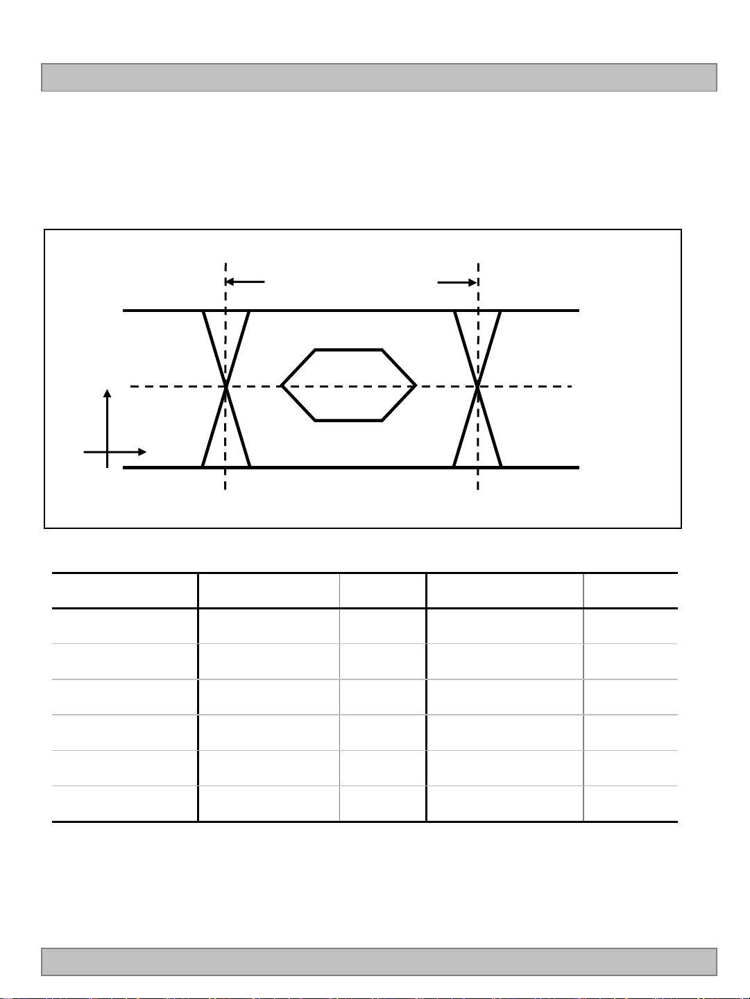
3-4. V by One input signal Characteristics
3-4-1. V by One Input Signal Timing Diagram
1UI = 1/(Serial data rate)
LD430EQE
Y
A
ㆍ
X
X=0 UI X=1 UI
Table7. Eye Mask Specification
X[UI] Note Y[mV] Note
A 0.25 (max) 2 0 -
B 0.3 (max) 2 50 3
C 0.7(min) 3 50 3
D 0.75(min) 3 0 -
B
ㆍ
C
ㆍ
ㆍ
ㆍ ㆍ
F E
D
Y=0mV
E 0.7(min) 3 l -50 l 3
F 0.3(max) 2 l -50 l 3
notes 1. All Input levels of V by One signals are based on the V by One HS Standard Ver. 1.4
2. This is allowable maximum value.
3. This is allowable minimum value.
4. The eye diagram is measured by the oscilloscope and receiver CDR characteristic must be
emulated.
- PLL bandwidth : 15 Mhz
- Damping Factor : 1
Ver. 1.0
11 /39

Product Specification
3-4-2. V by One Input Signal Characteristics
Vdiff =0
Lane0
LD430EQE
tRISK_INTER
Lane1
Vdiff =0
<Inter-pair Skew between two Lanes>
Description Symbol Min Max Unit notes
Allowable inter-pair skew between lanes tRISK_INTER - 5 UI 1,2
Notes 1.1UI = 1/serial data rate
2. it is the time difference of the differential voltage between any two lanes in one sub block.
Ver. 1.0
12 /39
 Loading...