

Page 1

COLOR TV
SERVICE MANUAL
CAUTION
BEFORE SERVICING THE CHASSIS,
READ THE SAFETY PRECAUTIONS IN THIS MANUAL.
CHASSIS : AC-05MB
MODEL : 30FS4D 32FS4D-UC
CANADA : http//biz.lgservice.com
USA : http//www.lgservice.com
: http//biz.lgservice.com
Page 2
- 2 -
SAFETY PRECAUTIONS
Many electrical and mechanical parts in this chassis have special safety-related characteristics. These parts are identified by in
the Schematic Diagram and Replacement Parts List.
It is essential that these special safety parts should be replaced with the same components as recommended in this manual to
prevent X-RADIATION, Shock, Fire, or other Hazards.
Do not modify the original design without permission of manufacturer.
General Guidance
An lsolation Transformer should always be used during
the servicing of a receiver whose chassis is not isolated from
the AC power line. Use a transformer of adequate power rating
as this protects the technician from accidents resulting in
personal injury from electrical shocks.
It will also protect the receiver and it's components from being
damaged by accidental shorts of the circuitary that may be
inadvertently introduced during the service operation.
If any fuse (or Fusible Resistor) in this TV receiver is blown,
replace it with the specified.
When replacing a high wattage resistor (Oxide Metal Film
Resistor, over 1W), keep the resistor 10mm away from PCB.
Keep wires away from high voltage or high temperature parts.
Due to high vacuum and large surface area of picture tube,
extreme care should be used in handling the Picture Tube .
Do not lift the Picture tube by it's Neck.
X-RAY Radiation
Warning:
To determine the presence of high voltage, use an accurate
high impedance HV meter.
Adjust brightness, color, contrast controls to minimum.
Measure the high voltage.
The meter reading should indicate
23.5
!1.5KV: 14-19 inch, 26!1.5KV: 19-21 inch,
29.0
!1.5KV: 25-29 inch, 30.0 ! 1.5KV: 32 inch
If the meter indication is out of tolerance, immediate service
and correction is required to prevent the possibility of
premature component failure.
Before returning the receiver to the customer,
always perform an AC leakage current check on the exposed
metallic parts of the cabinet, such as antennas, terminals, etc.,
to be sure the set is safe to operate without damage of
electrical shock.
Leakage Current Cold Check(Antenna Cold Check)
With the instrument AC plug removed from AC source,
connect an electrical jumper across the two AC plug prongs.
Place the AC switch in the on positioin, connect one lead of
ohm-meter to the AC plug prongs tied together and touch other
ohm-meter lead in turn to each exposed metallic parts such as
antenna terminals, phone jacks, etc.
If the exposed metallic part has a return path to the chassis, the
measured resistance should be between 1MΩ and 5.2MΩ.
When the exposed metal has no return path to the chassis the
reading must be infinite.
Any other abnormality that exists must be corrected before the
receiver is returned to the customer.
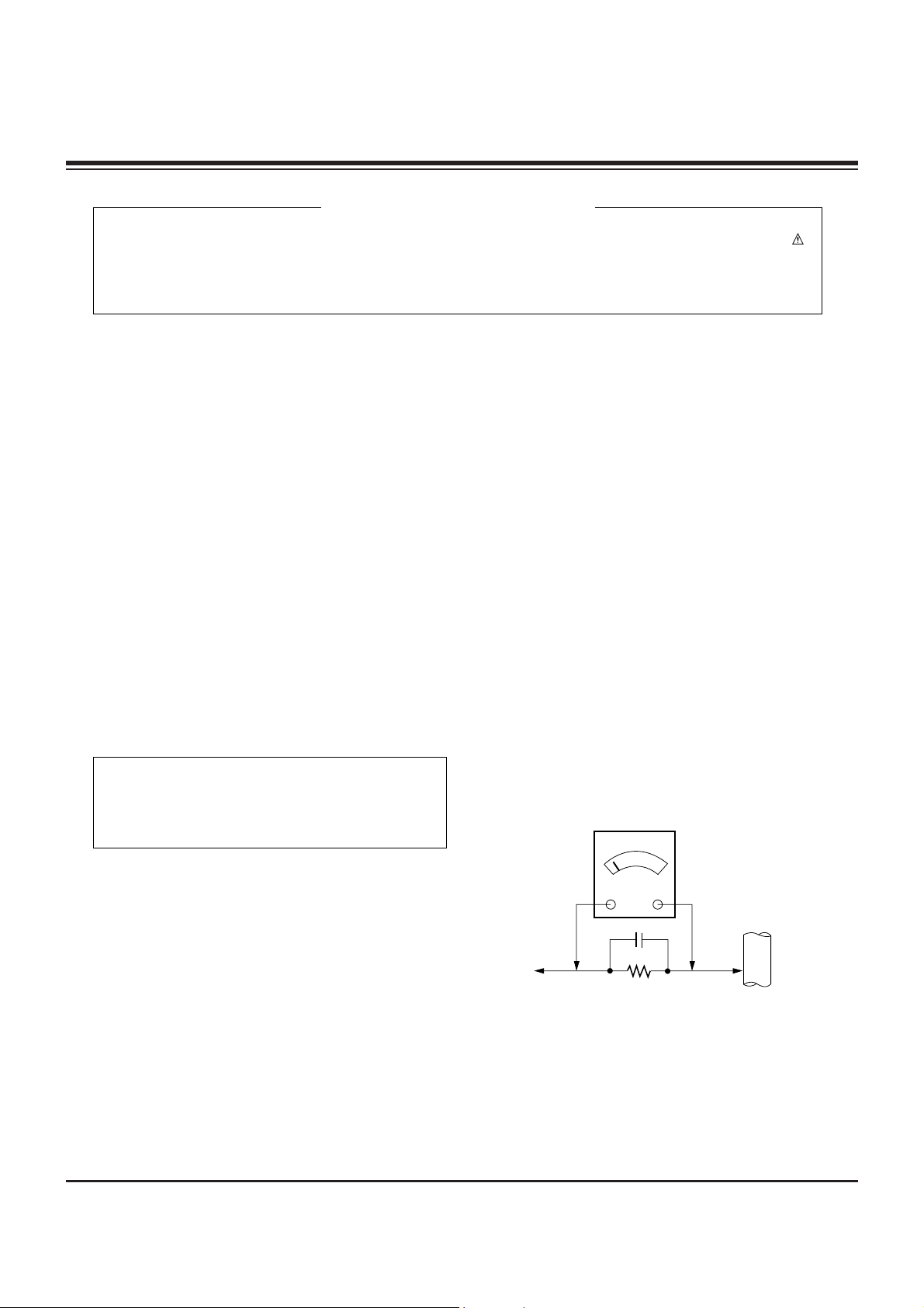
Leakage Current Hot Check (See below Figure)
Plug the AC cord directly into the AC outlet.
Do not use a line Isolation Transformer during this check.
Connect 1.5K/10watt resistor in parallel with a 0.15uF capacitor
between a known good earth ground (Water Pipe, Conduit, etc.)
and the exposed metallic parts.
Measure the AC voltage across the resistor using AC
voltmeter with 1000 ohms/volt or more sensitivity.
Reverse plug the AC cord into the AC outlet and repeat AC
voltage measurements for each esposed metallic part. Any
voltage measured must not exceed 0.75 volt RMS which is
corresponds to 0.5mA.
In case any measurement is out of the limits sepcified, there is
possibility of shock hazard and the set must be checked and
repaired before it is returned to the customer.
Leakage Current Hot Check circuit
CANADA: LG Electronics Canada, Inc. 550 Matheson
Boulevard East Mississauga, Ontario L4Z 4G3
USA : LG Customer Interactive Center
P.O.Box 240007, 201 James Record Road
Huntsville, AL 35824
Digital TV Hotline 1-800-243-0000
The source of X-RAY RADIATION in this TV receiver is the
High Voltage Section and the Picture Tube.
For continued X-RAY RADIATION protection, the
the Replacement Parts List.
IMPORTANT SAFETY NOTICE
0.15uF
To Instrument’s
exposed
METALLIC PARTS
AC Volt-meter
Good Earth Ground
such as WATER PIPE,
CONDUIT etc.
1.5 Kohm/10W
Page 3

- 3 -
DESCRIPTION OF CONTROLS...........................................4
SPECIFICATIONS.................................................................9
ADJUSTMENT INSTRUCTIONS ........................................10
PRINTED CIRCUIT BOARDS.............................................22
BLOCK DIAGRAMS............................................................29
EXPLODED VIEW...............................................................32
EXPLODED VIEW PARTS LIST.........................................33
REPLACEMENT PARTS LIST............................................34
SCHEMATIC DIAGRAMS.......................................................
TABLE OF CONTENTS
Page 4
- 4 -
Front Panel Controls
ON/OFF
Standby indicator (Illuminates brightly when the TV is in
standby mode. Dims when the TV is switched on.)
Remote control sensor
TV/VIDEO
MENU
VOL left/ right
Volume(
GG
) button increases the sound level and vol-
ume(
FF
) button decreases the sound level.
CH (Channel) up / down
1
2
3
4
These buttons work just as they do on
your remote control.
5
6
7
ON/OFF
MENU
VOL
CH
TV/
VIDEO
1
2
3
4
5
6
7
DESCRIPTION OF CONTROLS
Page 5
- 5 -
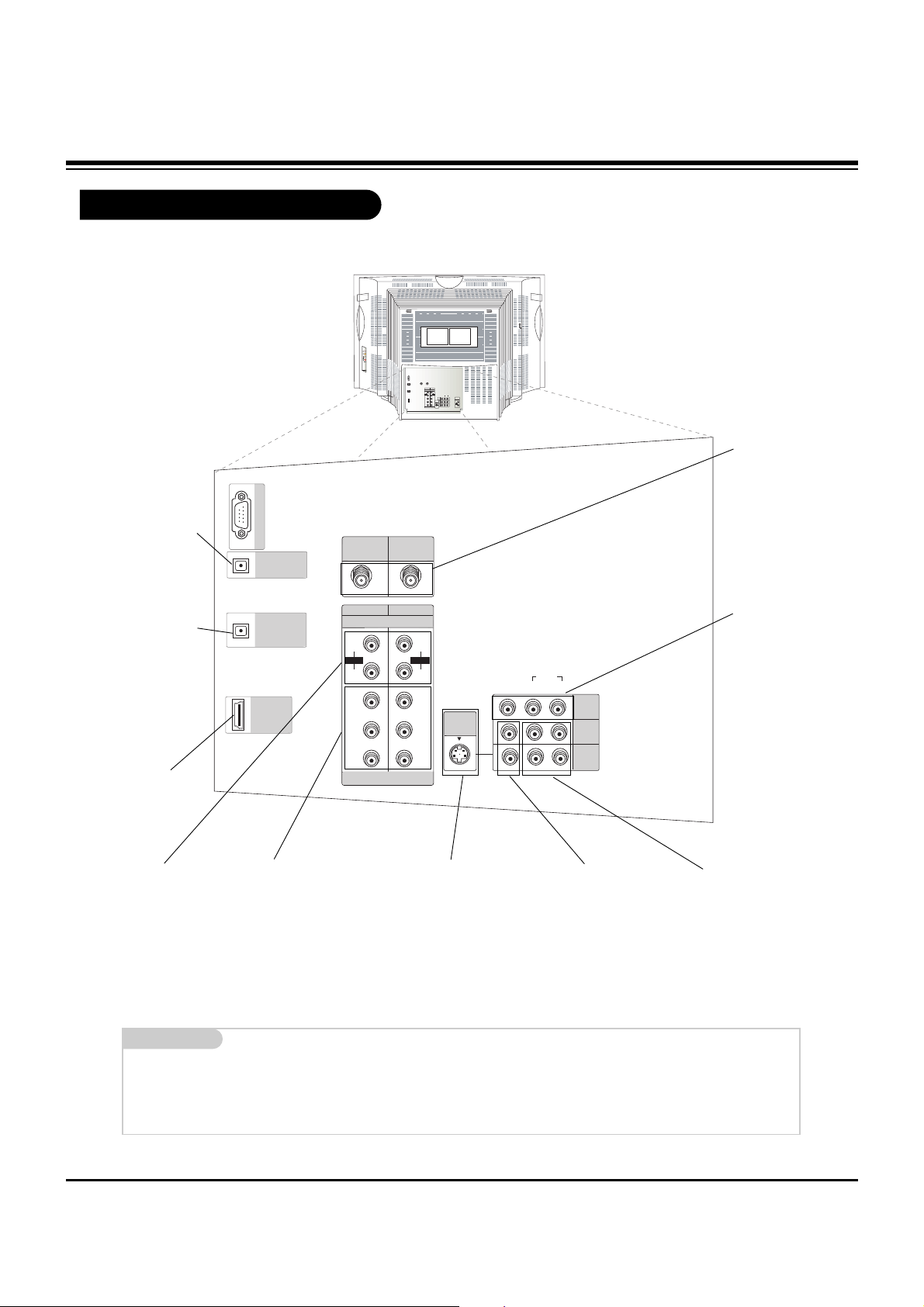
Rear Connections Panel
Mini glossary
JACK A connection on the back of a TV, VCR, or any other A/V device. This includes the RF jack and the Audio/Video jacks that are
color-coded.
SIGNAL Picture and sound traveling through cable, or over the air, to your television screen.
CALIBRATION
DIGITAL
AUDIO OUTPUT
OPTICAL
DVD/DTV INPUT
AUDIO
L(MONO)
CABLE
ANTENNA
HDMI/DVI
DIGITAL
AUDIO INPUT
OPTICAL
(DVI)
R
COMPONENT1
(480i/480p/720p/1080i)
COMPONENT2
S-VIDEO
MONITOR
OUTPUT
IN1
IN2
AUDIO
R
AUDIO
AUDIO
INPUT
VARIABLE
AUDIO
S-Video In
A connection available with some highend equipment that
provides even better
picture quality for
Video 1, Front Video.
RF Connectors:
Cable, Antenna
Used to connect
cable or antenna
signals to the television, either directly
or through your
cable box.
Video 1 and 2 Inputs
Connects the video signals from various types
of equipment.
Y, P
B, PR
DVD Component Video and HD
Component Video
Some top-of-the-line DVD players
use what is called “component
video,” for extremely accurate picture reproduction. Refer to your
DVD manual for further information.
Connecting external equipment to your TV.
Monitor Out
Connects to a second TV or Monitor.
Left/Right Audio
Used for stereo sound
from various types of
equipment.
Component Left/Right
Audio
Used for stereo sound
from various types of
equipment.
HDMI/DVI
Used to connect
from a DTV
source.
Digital Audio
Output Optical
Connects to exter-
nal audio equip-
ment like a home
theater system.
Digital Audio Input
Optical
Connects to digital
audio from various
types of equipment.
DESCRIPTION OF CONTROLS
C
A
L
I
B
R
A
T
I
O
N
DIGITAL
AUDIO OUTPUT
OPTICAL
DIGITAL
AUDIO INPUT
OPTICAL
(DVI)
HDMI
/DVI
CABLE ANTENNA
+75 Ω +75 Ω
COMPONENT1
COMPONENT2
(480i/480p/720p/1080i)
(R)
AUDIO
(L)
P
R
PB
Y
DVD/DTV INPUT
CALIBRATION
DIGITAL
AUDIO OUTPUT
OPTICAL
DIGITAL
AUDIO INPUT
OPTICAL
(DVI)
HDMI/DVI
AUDIO
CABLE
ANTENNA
++7575 ΩΩ ++7575 ΩΩ
COMPONENT1
COMPONENT2
(480i/480p/720p/1080i)
RR
RR
AUDIO
AUDIO
AUDIO
LL
LL
VIDEOVIDEO
L(MONO)
RR
VARIABLE
MONITOR
AUDIO
PP
R
R
PP
OUTPUT
S-VIDEO
LL
PP
BB
PP
BB
IN2
INPUT
AUDIO
RR
YY
YY
IN1
DVD/DTV INPUT
(R)
(L)
PR
S-VIDEO
INPUT
PB
Y
VIDEO
AUDIO
L(MONO) R
MONITOR
OUTPUT
IN2
IN1
Page 6
- 6 -
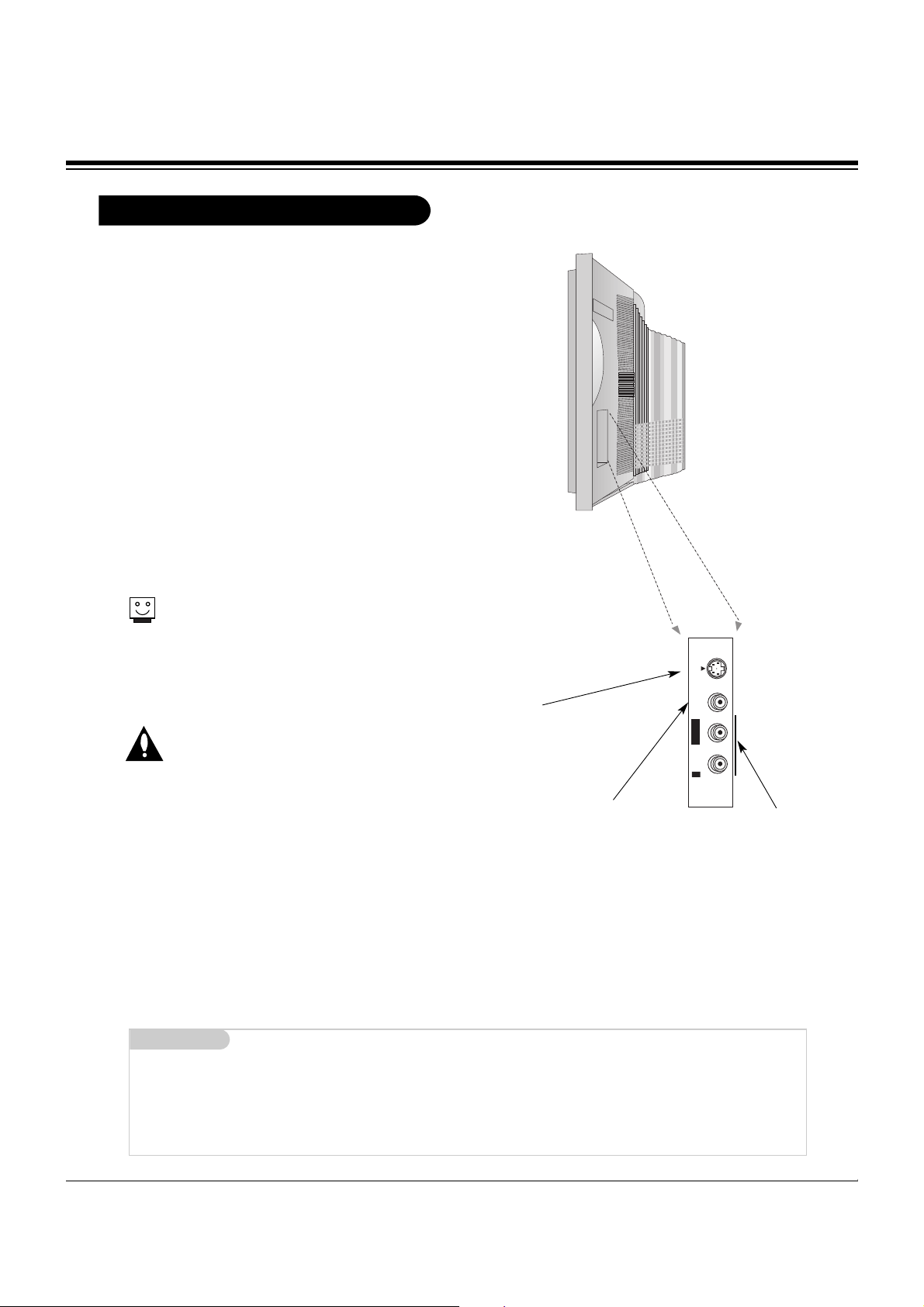
Side Connections Panel
There are four jacks on the lower-right front side
of your TV that make connecting Audio/Video
devices like video games and camcorders very
simple.
The jacks are like those found on the back jack
connection panel. This means that most equipment that connects to those types of jacks on
the rear jackpack, may be connected to the Side
connection panel (FRONT VIDEO).
To use the Side jacks as the signal source,
select them using Input source menu as
described on page 25. They will be named
“FRONT VIDEO” in the Input source menu.
Left/Right Audio
Used for stereo sound
from various types of
equipment.
Video in
Connects the video
signals from any
piece of equipment.
S-Video
A connection available on some very
high-end equipment that provides
better picture quality than video
input.
When you select Front Video
or Front S-Video, the Front
Audio inputs are automatically
selected as well.
Do not connect to both Video
and S-Video at the same time.
Connect either Video or SVideo only.
Mini glossary
A/V CABLES Audio/Video cables. Three cable connector—Right audio (red), Left audio (white), and Video (yellow). A/V cables are used
for stereo playback of videocassettes and for higher quality picture and sound from other A/V devices.
A/V DEVICE Any device that produces video (picture) and/or audio (sound) (VCR, DVD, cable box, or television).
DESCRIPTION OF CONTROLS
FRONT VIDEO Panel
S-VIDEO
VIDEO IN
L/MONO
AUDIO
R
FRONT VIDEO
Page 7
- 7 -
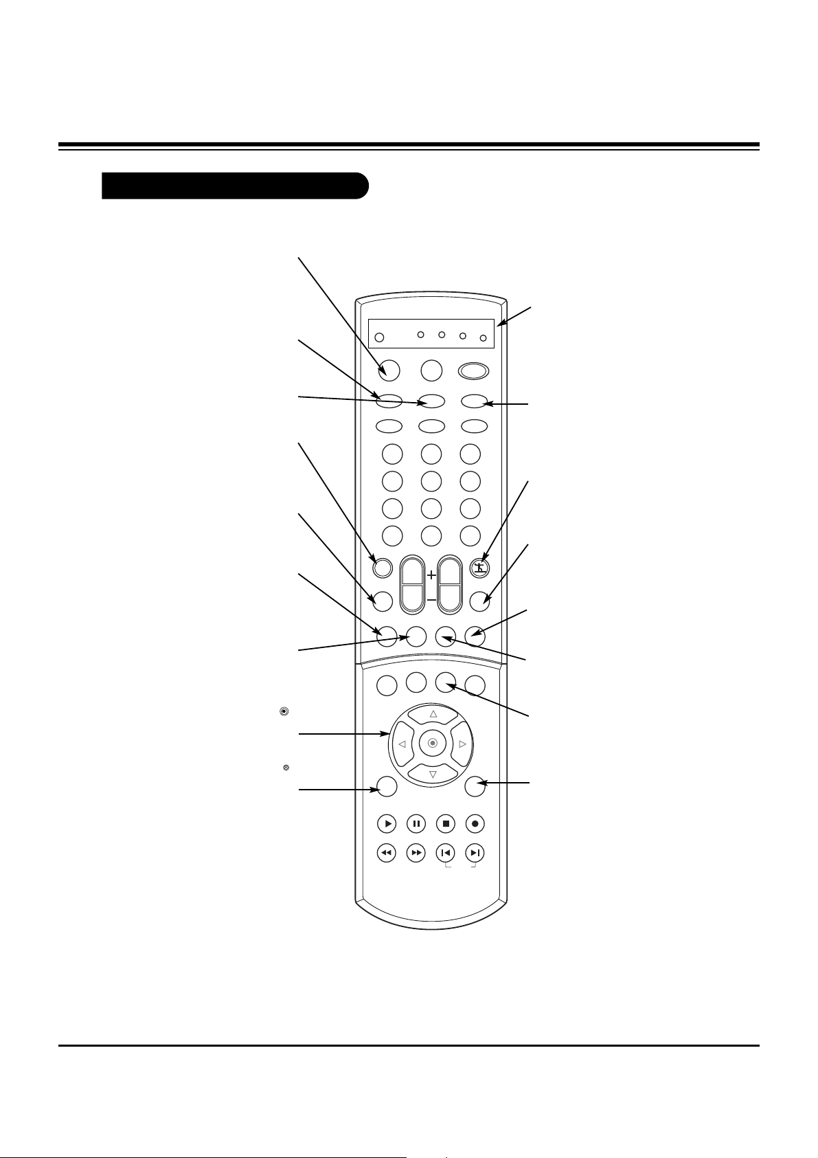
Remote Control Functions in TV Mode
FAV
Use to scroll the FAV channel list.
MENU
Brings up the main
menu to the screen.
EXIT
Clears all on-screen displays and returns to TV
viewing from any menu.
CC
Lets you select a closed caption
mode for displaying captioning
information when provided for
DTV/Analog signal.
EZ PIC
Adjusts the factory preset picture depending on the viewing environment.
SAP
Selects MTS sound: Mono, Stereo,
and SAP in analog mode.
Change the audio language in DTV
mode.
SURROUND
Selects : Off, 3D
EchoSound System and
SRS TruSurround XT.
MUTE
Switches the Mute or the EZ mute.
Mute: The sound is off. EZ mute:
Turns the sound off, and displays the
caption.
THUMBSTICK
(UP/DOWN/LEFT/RIGHT/ )
Allows you to navigate the on-screen
menus and to adjust the system settings
and preferences, by moving to an option
with
F G
and selecting the highlighted
option with .
TV INPUT
Switches TV mode or CATV
mode.
MODE
Selects the remote operating
mode: TV, VCR, Cable, DVD or
Satellite. Select other operating
modes, for the remote to oper-
ate external devices.
TV/VIDEO
Selects: Antenna, Cable,
Video1, Video2, Front video,
Component 1-2 and HDMI/DVI
input sources.
COMP1
Selects the Component 1
input source.
EZ SOUND
Selects the sound appropriate
for the program’s category.
FREEZE
Captures and freezes
the currently-viewed
picture.
RATIO
Changes the aspect ratio.
MODE INDICATOR
LIGHTS
Show active remote mode
every time any button is
pressed.
D
E
DESCRIPTION OF CONTROLS
CABLE
VCR
TV
MODE
TV INPUT
*
TV/VIDEO
HDMICOMP2
1 2 3
4 5 6
7 8 9
DASH(-)
MUTE
EZ SOUND
RATIO
INFO
MENU EXIT
PLAY
REW
0
VOL
TIMER CC
PAUSE
STOP
FF
CH
SKIP
DVD
SAT
POWER
COMP1
FRONT
FLASHBK
FAV
EZ PIC
SURROUNDFREEZE SAP
SIGNAL
RECORD
Page 8
- 8 -
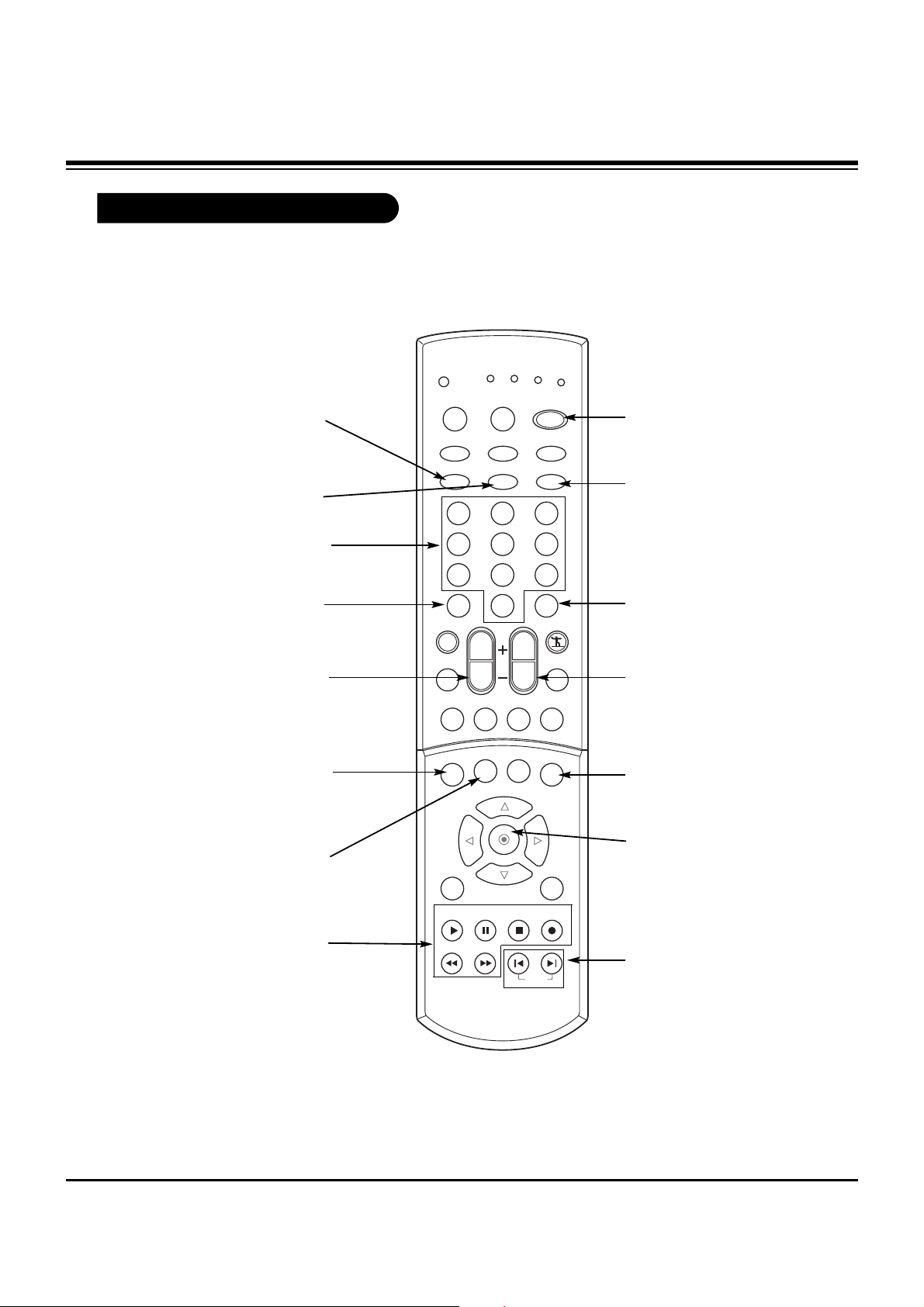
Remote Control Functions in TV Mode
POWER
Turns your TV or any other
programmed equipment on
or off, depending on mode.
CHANNEL UP/DOWN
Scrolls through available channels
present in EZ Scan memory.
NUMBER KEYPAD
For direct channel selection and
programming functions.
ENTER
When in the menu system
and other on-screen displays, selects highlighted
options.
RECORD, PAUSE, REW,
FFWD, PLAY, STOP
Control the functions on your VCR.
VOLUME UP/DOWN
Increases/decreases the sound
level.
INFO
When you watch the TV, displays
information on top of the screen.
Not available in Component 1-2
and HDMI/DVI.
SKIP LEFT/RIGHT
Playing CDs: Selects
songs.
Playing DVDs: Selects
movie chapters.
COMP2
Selects the Component 2 input
source.
HDMI
Selects the HDMI input source.
DASH(-)
Is used to enter a program
number for multiple program
channels such as 2-1,2-2,etc.
FLASHBK
Tunes to the previous channel
viewed.
TIMER
Lets you select the amount
of time before your TV
turns itself off automatically.
SIGNAL
Displays the digital signal
strength.
FRONT
Selects the front video
input source.
DESCRIPTION OF CONTROLS
VCR
TV
MODE
TV INPUT
TV/VIDEO
1 2 3
4 5 6
7 8 9
DASH(-)
MUTE
EZ SOUND
VOL
RATIO
TIMER CC
INFO
HDMICOMP2
*
0
CABLE
DVD
SAT
POWER
COMP1
FRONT
FLASHBK
FAV
EZ PIC
CH
SURROUNDFREEZE SAP
SIGNAL
MENU EXIT
PLAY
PAUSE
STOP
REW
FF
RECORD
SKIP
Page 9

- 9 -
Model 32FS4D-UC
Horizontal Size (inches) 36.14
Height (inches) 16.51
Thickness (inches) 23.13
Weight (pounds) 114.9
Power requirement AC 120V~ 60Hz
Television system American TV Standard, NTSC-M, Integrated ATSC tuner, 64 & 256 QAM
Television Channel VHF: 2 - 13
UHF: 14 - 69
CATV: 1 - 135
CADTV: 1 - 135
DTV: 2 - 69
Power consumption (W) 180W
Antenna 75 ohm external terminal for VHF/UHF
Audio Output (W) 7.5W x 2
Supplied accessories Remote control, batteries 2 size AA(Alkaline battery)
Screen Aspect Ratio 16 : 9
External input ports Video/Audio input (3 set)
Video output (1 set)
S-Video input (2)
Component input (2 set)
HDMI/DVI input (1)
Digital audio optical input (DVI)(1)
Digital audio optical output (1)
Calibration port (1)
Cable/Antenna port
Design and specifications are subject to change without prior notice.
Product Specifications
SPECIFICATIONS
Page 10
- 10 -
1. Application Object
These instructions are applied to the AC-05MB chassis.
2. Notes
(1) Because this is not a hot chassis, it is not necessary to use
an isolation transformer. However, the use of an isolation
transformer will help protect test instruments.
(2) Adjustments must be done in the correct order.
(3) The input voltage of the receiver must remain at
120V±10% while adjusting.
(4) The receiver must be operated for about 20 minutes prior
to the adjustment.
[ Never operate the set over 10 minutes with a still picture
because it may cause screen burn.
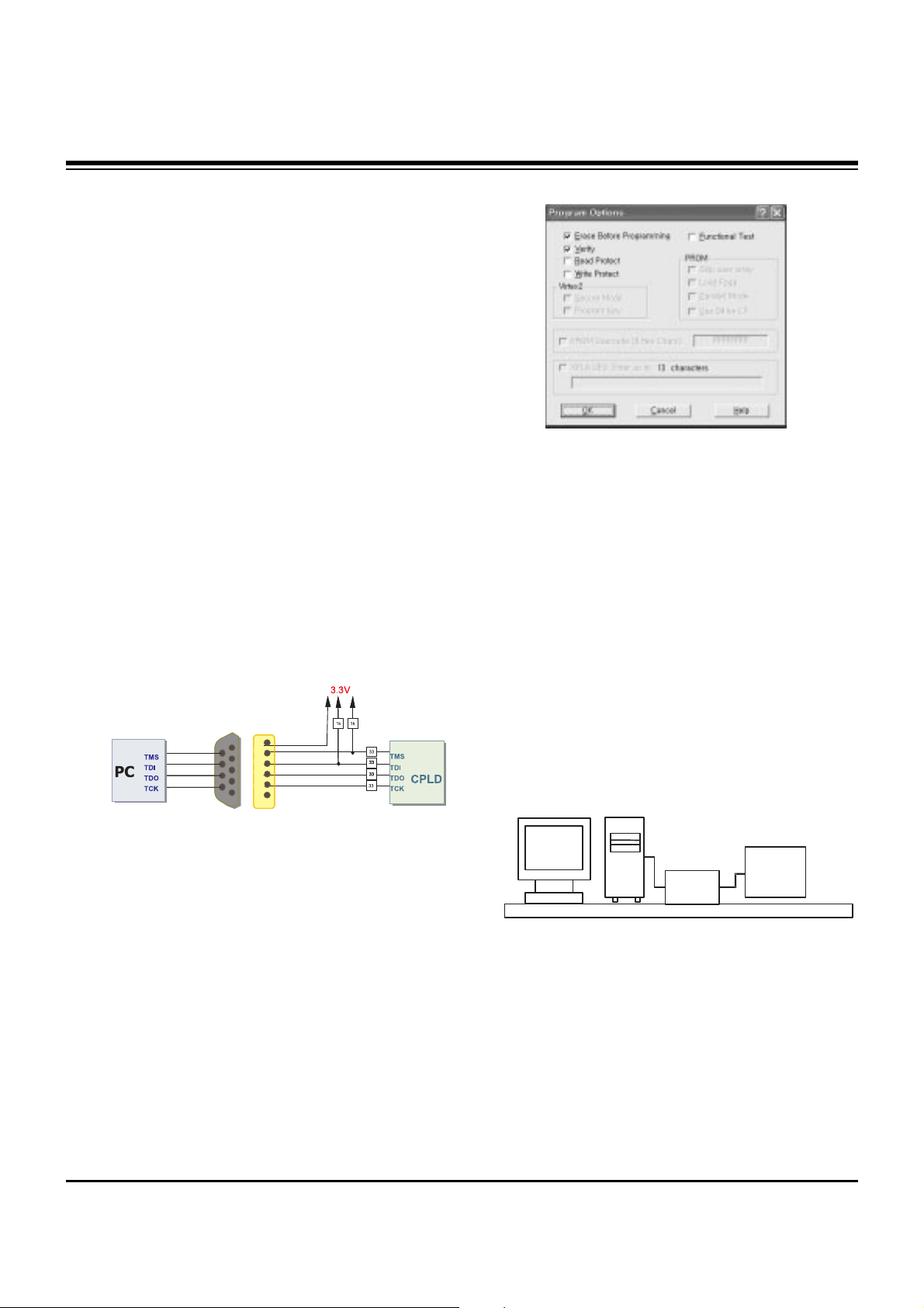
3. CPLD Download
3-1. Required Test Equipments &
Preparation for Adjustment
(1) Connect the PC and memory JIG as shown in <Fig. 1>.
(2) Turn on JIG MAIN POWER SW.
(3) Turn on the PC and monitor, operate the ‘Device
Programming’ software.
3-2. Adjustment Sequence
(1) Once the program is running, [OPTION MODE
SELECTION] is displayed in the window.
Check the “Load configuration File(.cdf, .pdr)” in this
window and click the finish button
(2) When the screen displays the open window, select the
suitable file(*.cdf) according to model.
(3) IC figure is change to green by clicking it.
(4) Select program options.
(5) Check the [Erase before programming] and [Verify] menu
as shown <Fig. 2> and press the OK button.
(6) At this time, the download starts. The download will finish
in about 10 seconds.
4. Hold down Operation Check
(1) This check step is implemented during the frame assembly
process.
(2) Check method: Short circuit the R1471 of Main2 JP
display part and check if it switches to ST-BY. (Install 30K
resistances in parallel to the R1471 on jig.)
5. EDID Data Input
5-1. Required Test Equipment
(1) PC, Jig for adjusting DDC. (256 bytes write)
(2) S/W for writing DDC(EDID data write & read)
5-2. Setting of Device
5-3. Adjustment
(1) Set devices as above and turn on the PC and JIG.
(2) Open S/W for writing DDC (EDID data write & read).
(3) Enter the Model-->Open in the Menu and then select EDID
DATA.
(4) Click the Digital and cancel the ANALOG.
Then connect to turn on the yellow light at the board &
connection.
(5) Click the Write Data & Verify and then download the EDID
DATA.
ADJUSTMENT INSTRUCTIONS
<Fig. 1 > How to connect the MEMORY JIG and PC
<Fig . 2>
PC
JIG
TV
SET
<Fig . 3>
Page 11
- 11 -
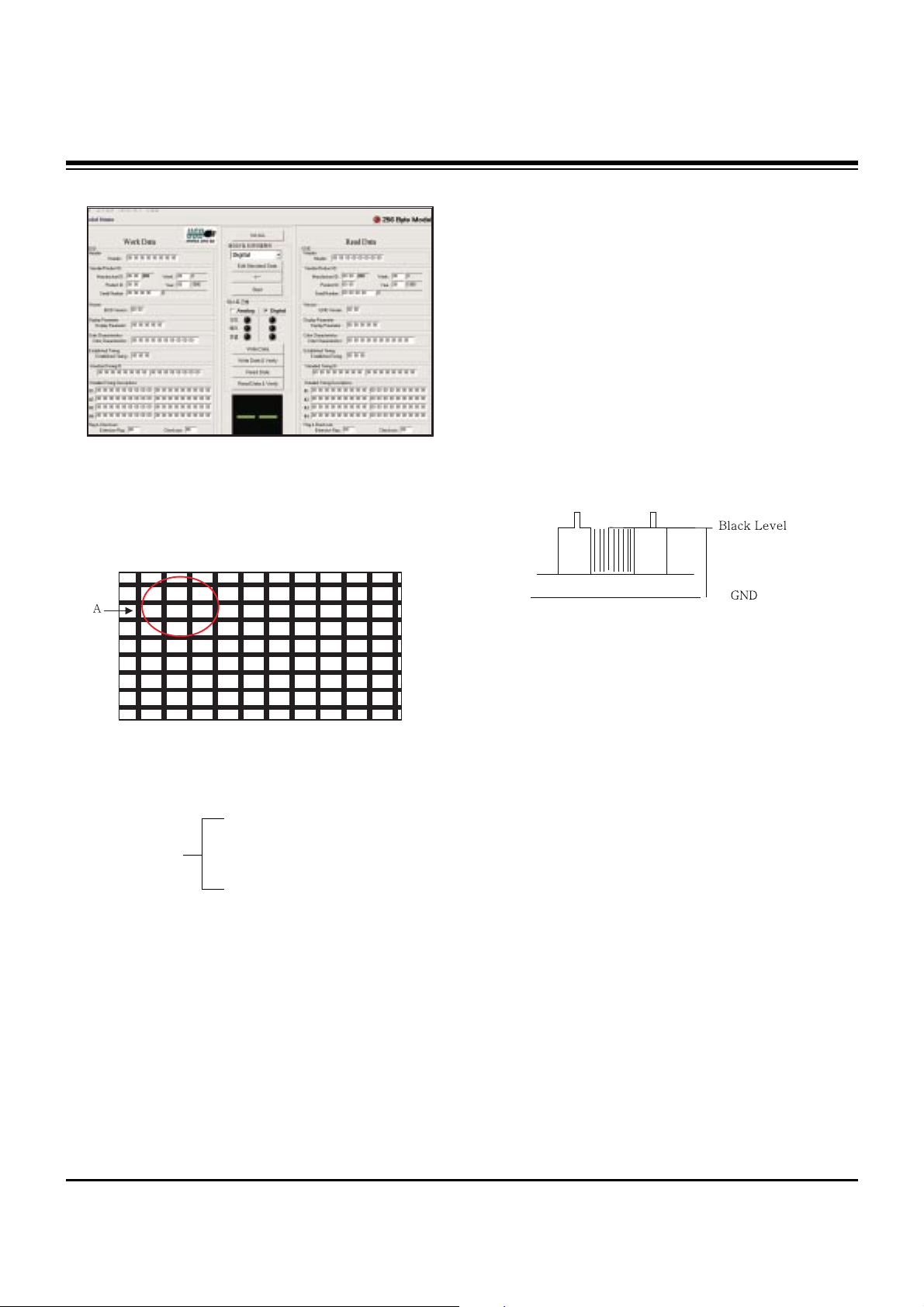
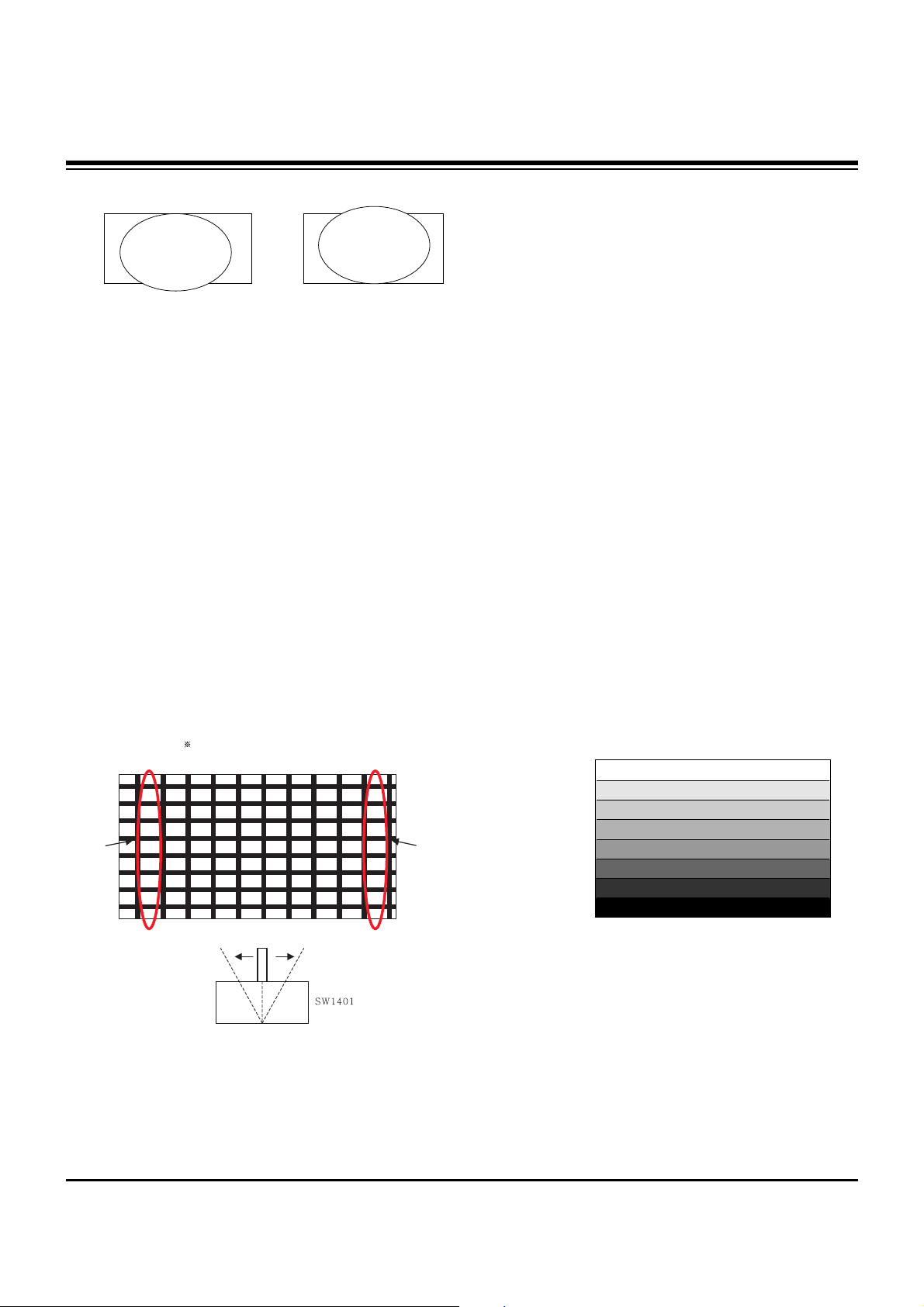
6. Focus Adjustment
(1) Set Picture condition to “Normal”.
CONTRAST : 100
BRIGHT : 60
Normal TINT : 60
COLOR : 0
SHARPNESS : 60
(2) Set the Aspect ratio to Wide Mode.
(3) Receive a Cross Hatch Pattern, adjusting the FOCUS
Knob on the flyback transformer for the best focus in the
area designated “A” above.
[ Heat run over 15 minutes before adjustment.
7. CUT-OFF Adjustment
(Screen Voltage Adjustment)
7-1. Test equipment
Oscilloscope, 100:1 Probe
7-2. Adjustment
(1) Select EZ Adjust 3. CUT-OFF, by pressing the ADJ key on
the SVC Remote control.
When it enters to adjustment mode, the pattern from a
signal generator is being selected, it becomes with Normal
image 16:9 and the CUT-OFF DRIVE data setting 31.
(2) Connect the oscilloscope ground lead to GND on the CPT
board and the probe to the GK pin connector of the CPT
socket.
Using the SCREEN knob on the Flyback Transformer,
adjust the black level voltage to 170±2V.
8. Deflection Adjustment
8-1. Preliminary Steps
Select EZ Adjust 1. Raster, Cent, H/V Size by using the ADJ
key on the SVC Remote control.
In the adjustment mode a Digital Pattern signal, NORMAL,
16:9 Screen is displayed.
8-2. Raster V-Center(V.Center) Adjustment
Select 62. V-Postition in the adjustment mode and adjust it to
position the vertical center line in vertical center of the CPT.
8-3. Vertical Deflection Size Adjustment
(Overscan : 10%)
(1) Select 59. V-SIZE in the adjustment mode.
(2) Adjust until the smaller inscribed circle coincides with the
outer frame of screen.
(3) Select 95. LO-VLIN or 94. UP-VLIN and adjust until the
larger inscribed circle coincides with the outer frame of
screen.
ADJUSTMENT INSTRUCTIONS
170±2V
<Fig . 6> CUT-OFF Adjustment
(SCREEN voltage adjustment OSCILLOSCOPE,
100:1 PROBE, VOLTS/DIV : 0.5V/DIV SEC/DIV : 5us,
The TRIGGER MODE it puts in the TV-H)
<Fig . 4>
<Fig . 5>
Page 12
- 12 -
8-4. Raster H-center(H.CENTER) Adjustment
Select 77. H Postion in the adjustment mode and adjust until
left and right screen are symmetrically equal.
8-5. Horizontal Deflection Size Adjustment
(1) Reduce 66 H-Size to verify screen protection (overscan)
on the right and left sides.
(2) Adjust the horizontal size, using a test pattern.
8-6. Horizontal Pincushion Adjustment
(1) Select EZ Adjust 2. Pin-Cushion(16:9) by pressing the ADJ
key on the SVC Remote control.
In the adjustment mode a Cross-Hatch Pattern, 16:9
Screen is displayed.
(2) Select PIN-PHASE, PIN-AMP, AFC-BOW, AFC-ANGLE,
UP-CPIN, LO-CPIN in the adjustment mode and adjust
until there is no Pincushion distortion or trapezoid distortion
on the screen.
8-7. HRS Switch Adjustment
(1) Change the Cross Hatch Pattern.
(2) If the linearity size width of A is narrow on the A or B,
change the SW1401 to the right.
And if the B is narrow, change the SW1401 to the left to
make the size width as same as A and B.
* If the neutral condition is alike, not to change, put the
position.
(3) Readjust the “1.Raster, Cent, H/V Size“ by pressing the
ADJ key of adjustment remote control.
(4) Readjust the “2.Pin-Cushion(16:9)“ by pressing the ADJ
key of adjustment remote control.
8-8. Pincushion Adjustment (4:3 Mode)
(1) Change the Digital Pattern.
(2) Select EZ Adjust 3. Pin-Cushion(4:3) by pressing the ADJ
key on the SVC Remote control.
In the adjustment mode a Digital Pattern signal, NORMAL,
4:3 Screen is displayed.
(3) 4:3 Pin cushion Adjustment
Adjust the 4 adjustment item to be straight without distortion
left/right line of 4:3 Screen
1) 4 Adjustment Item: Pin-Amp, Pin-Phase, Up-Cpin, LoCpin
2) Initial Data of 4 Adjustment Item: 0
9. Component MST3000 Offset/Gain
Adjustment
9-1. Test Equipment
801GF(802B, 802F, 802R) Pattern Generator or MASTER
Pattern Generator
9-2. Preliminary Steps
(1) Turn the power supply on.
(2) Enter the Component mode.
(3) Receive the “1080I” Format, “Hoz30Bar” Pattern of the
Video Pattern Generator.
(4) Certainly, adjust the output signal in state of 700mVp-p
±10mV.
ADJUSTMENT INSTRUCTIONS
L-LIN U-LIN
A(Left) B(Right)
This screen is reflected picture
at the position of worker
RightLeft
Neutrality
<Fig . 7>
<Fig . 8>
100% White
100% Yellow
100% Cyan
30% Gray
30% Gray
100% Red
100% Blue
Black
<Fig . 9> 1080I Format, Hoz30Bar Pattern
Page 13
- 13 -
9-3. ADC Offset Adjustment
(1) After receiving a signal press the ADJ Key on the SVC
Remote Control repeatedly to acess the Adjustment mode.
(2) Adjustment will set the automatically by pressing the
“8.MST3000-Set” of adjustment item.
(3) After finishing the adjustment, output the “MST3000-OK”
OSD on the screen.
10. White Balance Adjustment
10-1. Preparation for Adjustment
(1) Perform the Screen Voltage Adjustment first.
(2) The White Balance it executes from automatic adjustment
hour Normal image condition.
(3) Start adjustments from initial setting of R.DRIVE=31,
G.DRIVE=31, B.DRIVE=31, R.CUT=31, G.CUT=31,
B.CUT=31.
(4) For manual adjustment, refer to the following procedure.
10-2. Adjustment
(1) Receive the White Pattern.
(2) Set screen size to wide mode(16:9).
(3) Select EZ Adjust 2.White Balance by pressing IN-START
Key on the SVC Remote control.
(4) Adjustment
1) Using the SVC Remote control, set the DCOL value of
CXA2150 to the “0”.
2) Set an image with Normal image.
3) Adjust R-DRIVE and B-DRIVE data so the color
coordinates in High light are the values in Table below.
(Bright Level : 35fl)
4) Adjust “CONTRAST” and “BRIGHT” so the bright level is
4.5±0.5F.L.
5) Adjust R-CUT and B-CUT data so the color coordinates
in Low light are the values in Table below.
6) Repeat 2)~ 5) until the color coordinates in High and
Low color satisfies the Table.
7) Check the adjusted color coordinates with the white
balance meter.
High Light : x=287
!
3, y=293!3
Low Light : x=287
!
3, y=293!3
Color temperature : 9,000K!
1000(-5MPCD)
11. Sub Bright, TINT, COLOR
Adjustment
11-1. Sub Bright Adjustment
(1) Select EZ Adjust 5. Sub Bright pressing ADJ key on the
SVC Remote control.
(2) Adjust to the point where “2” is not visible.
(3) Completed the adjustment, exit the adjustment mode using
ADJ Key.
11-2. Sub COLOR, TINT Adjustment
(1) Select EZ Adjust 6. Sub Tint, Color pressing ADJ key on
the SVC Remote control.
(2) Select SUB COLOR and adjust the 1 and 1’ portion not to
be classified.
(3) Select SUB TINT and adjust the 3 and 3’ portion not to be
classified.
(4) Completed the adjustment, exit the adjustment mode using
ADJ Key.
ADJUSTMENT INSTRUCTIONS
WHITE
B M C WBK BK BK
1
1'
3
3'
GREEN
MAGENTA
CYAN BLUERED
YELLOW
0 12 34 5 76 8 9
US14CH
Page 14
- 14 -
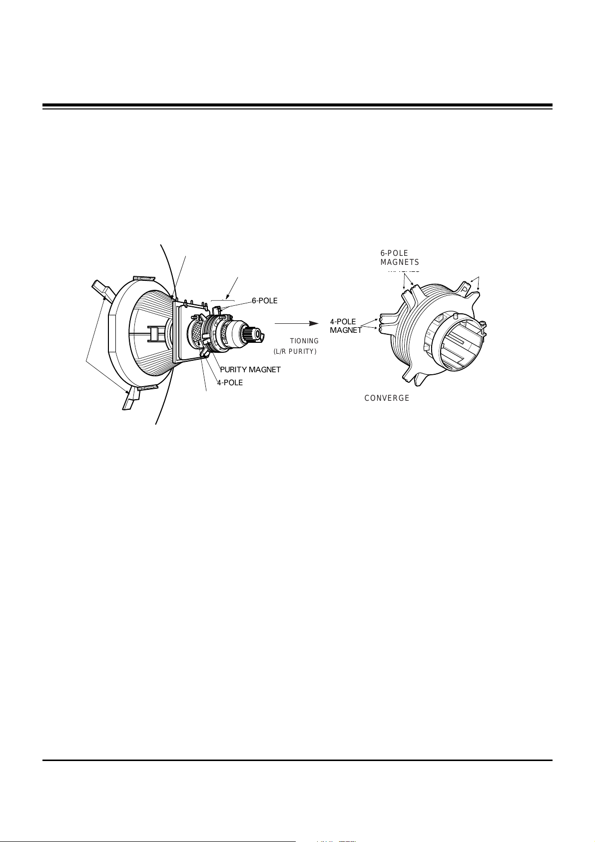
PURITY & CONVERGENCE ADJUSTMENT
Caution:
Convergence and Purity have been factory aligned. Do not
attempt to tamper with these alignments.
However, the effects of adjacent receiver components, or
replacement of picture tube or deflection yoke may require the
readjustment of purity and convergence.
¯ Purity Adjustment
This procedure DOES NOT apply to bonded yoke and picture
tube assemblies.
The instrument should be at room temperature (60 degrees F or
above) for six (6) hours and be operating at low beam current
(dark background) for approximately 20 to 30 minutes before
performing purity adjustments.
CAUTION: Do not remove any trim magnets that may be
attached to the bell of the picture tube.
1. Remove the AC power and disconnect the internal
degaussing coil.
2. Remove the yoke from the neck of the picture tube.
3. If the yoke has the tape version beam bender, remove it and
replace it with an adjustable type beam bender (follow the
instructions provided with the new beam bender)
4. Replace the yoke on the picture tube neck, temporarily
remove the three (3) rubber wedges from the bell of the
picture tube and then slide the yoke completely forward.
5. Reconnect the internal degaussing coil.
6. Position the beam bender locking rings at the 9 o'clock
position and the other three pairs of tabs (2,4 and 6 pole
magnets) at the 12 o'clock position.
7. Perform the following steps, in the order given, to prepare the
receiver for the purity adjustment procedure.
a. Face the receiver in the "magnetic north" direction.
b. Externally degauss the receiver screen with the television
power turned off.
c. Turn the television on for approximately 10 seconds to
perform internal degaussing and then turn the TV off.
d. Unplug the internal degaussing coil. This allows the
thermistor to cool down while you are performing the purity
adjustment. DO NOT MOVE THE RECEIVER FROM ITS
"MAGNETIC NORTH" POSITION.
e. Turn the receiver on and obtain a red raster by increasing
the red bias control (CW) and decreasing the bias controls
for the remaining two colors (CCW).
f. Attach two round magnets on the picture tube screen at 3
o'clock and 9 o'clock positions, approximately one (1) inch
from the edge of the mask (use double-sided tape).
DEFLECTION YOKE
PURITY &CONVERGENCE
MAGNET ASSEMBLY
RUBBER
WEDGES
GLASS CLOTH TAPE
PURITY MAGNET
6-POLE
4-POLE
4-POLE
MAGNET
CONVERGENCE MAGNET ASSEMBLY
6-POLE
MAGNES
PURITY MAGNET(2-POLE)
X-AXIS YOKE
POSITIONING
(L/R PURITY)
6-POLE
MAGNETS
CONVERGENCE MAGNET ASSEMBLY
Page 15
- 15 -
8. Referring to above, perform the following two steps:
a. Adjust the yoke Z-axis to obtain equal blue circles.
b. Adjust the appropriate beam bender tabs to obtain correct
purity (four equal circles).
9. After correct purity is set, tighten the yoke clamp screw and
remove the two screen magnets.
10. Remove the AC power and rotate the receiver 180 degrees
(facing "magnetic south").
11. Reconnect the internal degaussing coil.
12. Turn the receiver on for 10 seconds (make sure the receiver
came on) to perform internal degaussing, and then turn the
receiver off.
13. Unplug the internal degaussing coil.
14. Turn the receiver on and check the purity by holding one (1)
round magnet at the 3 o'clock and a second round magnet at
9 o'clock position. If purity is not satisfactory, repeat steps 8
through 14.
15. Turn off the receiver and reconnect the internal degaussing coil.
¯ Convergence Adjustment
Caution: This procedure DOES NOT apply to bonded yoke and
picture tube assemblies.
Do not use screen magnets during this adjustment
procedure. Use of screen magnets will cause an
incorrect display.
1. Remove AC power and disconnect the internal degaussing coil.
2. Apply AC Power and set the brightness to the Picture Reset
condition. Set the Color control to minimum.
3. Make horizontal line.
4. Adjust the Red, Green and Blue Bias controls to get a dim
white line.
5. Restore the screen by removing the horizontal line.
6. Reconnect the internal degaussing coil and apply AC power.
7. Turn the receiver on for 10 seconds to perform internal
degaussing and then turn the receiver off again.
8. Unplug the internal degaussing-coil.
9. Turn the receiver on, connect a signal generator to the VHF
antenna terminal and apply a crosshatch signal.
Caution: During the convergence adjustment procedure, be
very careful not to disturb the purity adjustment tabs.
Purity should be confirmed before proceeding with the
convergence adjustments.
Note:
Make sure the focus is set correctly on this instrument
before proceeding with the following adjustment.
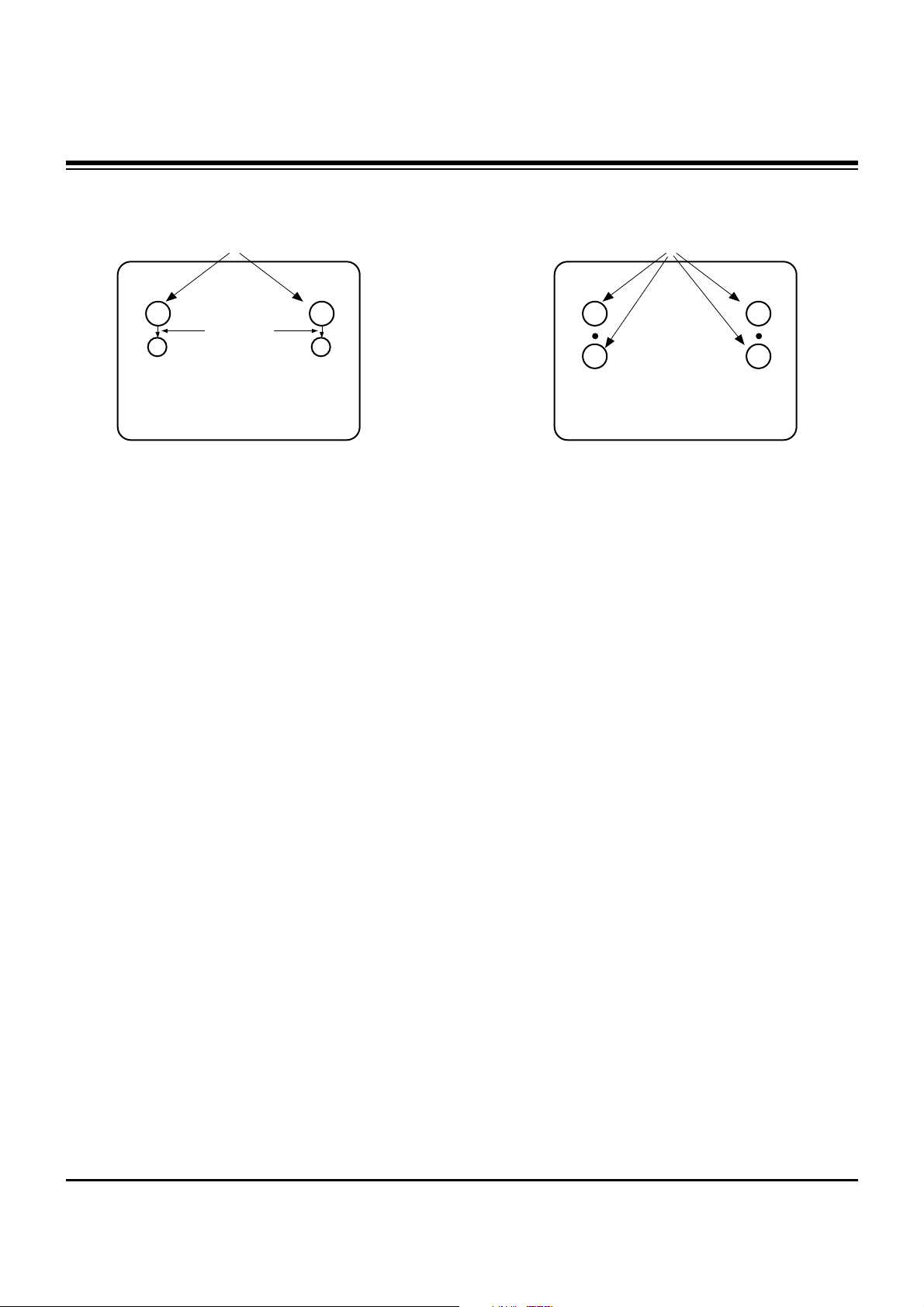
10. Converge the red and blue vertical lines to the green vertical
line at the center of the screen by performing the following
steps (below TABLE).
a. Carefully rotate both tabs of the 4-pole ring magnet
simultaneously in opposite directions from the 12 o'clock
position to converge the red and blue vertical lines.
b. Carefully rotate both tabs of the 6-pole ring magnet
simultaneously in opposite directions form the 12 o'clock
position to converge the red and blue (now purple)
vertical lines with the green vertical line.
11. Converge the red and blue horizontal with the green line at
the center of the screen by performing the following steps.
(below TABLE)
a. Carefully rotate both tabs of the 4-pole ring magnet
simultaneously in the same direction (keep the spacing
between the two tabs the same) to converge the red and
blue horizontal lines.
b. Carefully rotate both tabs of the 6-pole ring magnet
simultaneously in same direction (keep the spacing between
the two tabs the same) to converge the red and blue (now
purple) horizontal lines with the green horizontal line.
c. Secure the tabs previsouly adjusted by locking them in
place with the locking tabs on the beam bender.
MAGNETS
RED RED
1.ADJUST YOKE Z-AXIS FIRST
TO GET EQUAL BLUE
COLOR CIRCLES
2 .ADJUST BEAM BENDER 2 POLE
MAGNET TO GET FOUR EQUAL
COLOR CIRCLES
PURITY & CONVERGENCE ADJUSTMENT
Page 16

- 16 -
RING
PAIRS
4
POLE
ROTATION DIRECTION
OF BOTH TABS
OPPOSITE
SAME
OPPOSITE
SAME
MOVEMENT OF RED
AND BLUE BEAMS
B B
RR
OR
OR
B R B R
OR
B
R
B
R
B R
OR
B
R
6
POLE
12. While watching the 6 o'clock positions on the screen, rock the
front of the yoke in a vertical (up/down) direction to converge
the red and blue vertical lines. (Fig upper left)
13. Temporarily place a rubber wedge at the 12 o'clock position
to hold the vertical position or the yoke.
14.
Check the 3 o'clock and 9 o'clock areas to confirm that the red
and blue horizontal lines are converged.
If the lines are not converged, slightly offset the vertical tilt of the
yoke (move the rubber wedge if necessary) to equally balance the
convergence error of the horizontal lines at 3 o'clock and 9 o'clock
and the vertical lines at 6 o'clock and 12 o'clock.
15. Place a 1.5 inch piece of glass tape over the rubber foot at
the rear of the 12 o'clock wedge.
16. While watching the 6 o'clock and 12 o'clock areas of the
screen, rock the front of the yoke in the horizontal (left to
right) motion to converge the red and blue horizontal lines.
(Fig. upper right)
17. Temporarily place a rubber wedge at the 5 o'clock and 7
o'clock positions to hold the horizontal position of the yoke.
18. Check the 3 o'clock and 9 o'clock areas to confirm that the
red and blue vertical lines are converged. If the lines are not
converged, slightly offset the horizontal tilt of the yoke (move
the temporary rubber wedges if necessary) to equally
balance the convergence error of the horizontal lines at 6
o'clock and 12 o'clock and the vertical lines at 3 o'clock and 9
o'clock.
19. Using a round magnet confirm purity at the center, right and
left sides and corners. See Purity Adjustment Procedure.
20. Reconfirm convergence and apply a 1.5 inch piece of glass
tape over the rubber foot at the rear of the 5 o'clock and the 7
o'clock wedges.
RED
BLUE
RED BLUE
BLUE
RED
GREEN
GREEN
BLUE RED
GREEN
GREEN
ADJUSTMENT
VIEWING
AREA
UP/DOWN ROCKING OF THE YOKE
CAUSES OPPOSITE ROTATION OF RED
AND BLUE RASTERS
ADJUSTMENT
VIEWING
AREA
RED
RED
GREEN
TV
SCREEN
LEET/RIGHT ROCKING OF THE YOKE
CAUSES OPPOSITE SIZE CHANGE OF
THE RED AND BLUE RASTERS
UP/DOWN ROCKING OF THE YOKE CAUSES
OPPOSITE ROTATION OF RED AND BLUE
RASTERS
LEFT/RIGHT ROCKING OF THE YOKE
CAUSES OPPOSITE SIZE CHANGE OF
THE RED AND BLUE RASTERS
PURITY & CONVERGENCE ADJUSTMENT
Page 17

- 17 -
12. Service Mode Adjustment Data
(SVC Remote control ‘ADJ’ Key)
(1) Raster, Center, H/V_Size Data
(2) Pin-Cushion Data
ADJUSTMENT INSTRUCTIONS
NO OSD DATA
1 V-POSITION 26
2 V-SIZE 20-->25
3 H-POSITION 33
4 H-SIZE 27
5 UP-VLIN 5
6 LO-VLIN 4
7 PIN-AMP 30
8 PIN-PHASE 22
9 UP-CPIN 35
10 LO-CPIN 36
11 AFC-BOW 32
12 AFC-ANGLE 30
NO OSD
[16:9 Mode]
DATA
1 V-POSITION 26
2 V-SIZE 20
3 H-POSITION 33
4 H-SIZE 27
5 UP-VLIN 5
6 LO-VLIN 4
7 PIN-AMP 30
8 PIN-PHASE 22
9 UP-CPIN 35
10 LO-CPIN 36
11 AFC-BOW 32
12 AFC-ANGLE 30
NO OSD
[4:3 Mode]
DATA
1 Pin_Amp 0
2 Pin_Phase 0
3 Up_CPin 0
4 Lo_CPin 0
Page 18

- 18 -
(3) W/B Data
(4) SUB-BRIGHT: 20-->18
(5) SUB-TINT/COLOR
SUB-TINT: 12
SUB-COLOR: 8
ADJUSTMENT INSTRUCTIONS
NO OSD DATA
1 R-DRIVE 31
2 G-DRIVE
31(Fix.)
3 B-DRIVE 31
4 R-CUTOFF 31
5 G-CUTOFF
31(Fix.)
6 B-CUTOFF 31
Page 19

- 19 -
ADJUSTMENT INSTRUCTIONS
13. Service Mode Adjustment Data
(SVC Remote control ‘IN-START’ Key)
(1) CXA2150
NO ITEM
Initial
Data
Initial
Data
Initial
Data
NO ITEM NO ITEM
* SYSTEM RF/AV/480i/480p: 2
HD 720p/1080i: 3
SHP-F0 SD:1, HD: 0
* LTI_LEV: Digital Preset Mode: 3
Other Mode: 2
Page 20

NO ITEM
Initial
Data
NO ITEM
Initial
Data
NO ITEM
Initial
Data
NO ITEM
Initial
Data
- 20 -
ADJUSTMENT INSTRUCTIONS
(2) TeckWell IC(TW9919)
(3) NEC IC(uPD64011)
Page 21

- 21 -
NO ITEM
Initial
Data
NO ITEM
Initial
Data
ADJUSTMENT INSTRUCTIONS
(4) MST3000(ADC_IC)
Page 22

- 22 -
PRINTED CIRCUIT BOARD
MAIN(TOP)
Page 23

- 23 -
PRINTED CIRCUIT BOARD
MAIN(BOTTOM)
Page 24

- 24 -
POWER
PRINTED CIRCUIT BOARD
Page 25

- 25 -
DIGITAL(TOP)
PRINTED CIRCUIT BOARD
Page 26

- 26 -
DIGITAL(BOTTOM)
PRINTED CIRCUIT BOARD
Page 27

- 27 -
PRINTED CIRCUIT BOARD
V-FOCUS
SIDE A/V
POWER S/W
Page 28

- 28 -
PRINTED CIRCUIT BOARD
CONTROL
CPT
LED/IR
Page 29

- 29 -
BLOCK DIAGRAM
–
Page 30

- 30 -
BLOCK DIAGRAM
Page 31

- 31 -
NOTES
Page 32

- 32 -
EXPLODED VIEW
112
913
170
150
510
501
550
503
943
400
300
101
120
310
570
600
580
540
174
530
520
560
504
331
330
320
Page 33

- 33 -
EXPLODED VIEW PARTS LIST
101 4810V01503A BRACKET,CRT 32FS3D AC05MA HIPS 40AF .
112 6335932003A CPT ASSEMBLY,W76ERS270XV1 N(+0.40G) 0G TINT DOUBLE
6335932003B CPT,ITCW76ERS270XV1 L 32INCH SUPER-SLIM 0.50G 4/3
120 6400VA0025F SPEAKER,FULLRANGE C163A01K1452 8OHM 15/20W 86DB OTHERS 32FS2D
150 EAP30771101 Coil,Degaussing 32INCH SUPER SLIM AT 110V ADD SPONGE
170 6868900001A EARTH,CRT 32INCH 2POINT TIN WIRE BRAID 144TS 32FS1D
174 64109UH002A POWER CORD,LP-208RW+YFH800-02 2400MM HOUSING BLACK
300 30919E0029B CABINET ASSEMBLY,32FS4D-UC NO BRAND
310 5020V01110A BUTTON,CONTROL 32FS2D-NA ABS, HF-380 6KEY .
320 320-062E SPRING,KNOB
330 5020V01111A BUTTON,POWER 32FS2D-NA ABS, HF-380 1KEY .
331 4810V01272B BRACKET,32FS2D AC05MA ABS, AF-303S POWER, BRACKET
400 3809900135B BACK COVER ASSEMBLY,32FS4D-UC
501 4810V01239A BRACKET,BOARD 32FS2D AC05MA HIPS 40AF .
503 4811V00359J BRACKET ASSEMBLY,REAR AV 32FS2D-UC AC05MB SUPER SLIM
504 351-008A LINK,POWER S/W FOR MC-97A CHASSIS
510 6871VSMZZ4D PCB Assembly,Sub CPT M.I AC05MB 32FS4D-UC AUSLLA CPT B/D
520 68719MM061B PCB ASSEMBLY,MAIN AC05MB 32FS2D-UC AUXLLAX M/I
68719MM061C PCB Assembly,MAIN1 M.I AC05MB 32FS4D-UC CANADA ACCLLA M/I
530 68719DM006A PCB ASSEMBLY,MAIN2 M.I AC05MB 32FS4D-UC AUSLLA MAIN2 ASSY
540 68719SM122A PCB ASSEMBLY,SUB AC05MA 32FS2D-NA AKRLLA HRS/CS
550 68719SM170B PCB ASSEMBLY,SUB AC05MA 32FS2D-UC AKRLLA DIGITAL NEC
560 68719SM153A PCB ASSEMBLY,SUB POWER M.I AC05MB 32FS2D-UB AUSLLAX POWER SW
570 68719SM067A PCB ASSEMBLY,SUB AC05MA 32FS2D AKRLLAK CONTROL
580 68719SM068B PCB ASSEMBLY,SUB AC05MA 32FS4D AKRLLAK LED/PRE AMP
600 68719SM121A PCB ASSEMBLY,SUB AC05MA 32FS2D-NA AKRLLA SIDE A/V
943 1PTF0403116 SCREW TAP TITE(P),TRUSS HEAD
No.
Part No.
Description
Page 34

- 34 -
REPLACEMENT PARTS LIST
LOCA. NO PART NO DESCRIPTION
IC805
IC806
IC807
IC831
IC900
IC901
IC901
IC902
IC902
IC903
Q100
Q102
Q104
Q1106
Q1203
Q1204
Q1205
Q1206
Q1208
Q1211
Q1402
Q1406
Q1407
Q1408
Q1409
Q1410
Q1504
Q1505
Q1601
Q1604
Q1605
Q1606
Q1607
Q1610
Q1901
Q1902
Q1903
Q1904
Q1905
Q1906
Q1907
Q1920
Q1921
Q203
Q204
Q206
0ISH092100B
0ISH122100B
0IPMG00006A
0ILI817000G
0IPRPNE008A
0IPRPFA015B
0IPH612000B
0IPH612000B
0IPMGSG018C
0IPH612000B
0TR102008AA
0TR387500AA
0TR387500AA
0TR319809AA
0TR150400BA
0TR387500AA
0TR319809AA
0TR387500AA
0TR387500AA
0TR387500AA
0TF200000AA
0TR319809AA
0TR126609AA
0TRTH10007A
0TR127409AB
0TRKE10013A
0TR387500AA
0TR387500AA
0TR150400BA
0TR387500AA
0TR387500AA
0TR387500AA
0TR387500AA
0TR102009AM
0TR319809AA
0TR387500AA
0TR387500AA
0TR387500AA
0TR319809AA
0TR319809AA
0TR387500AA
0TR322800AB
0TRFC10001A
0TR387500AA
0TR150400BA
0TR387500AA
PQ09RD21 4SIP
PQ12RD21 4SIP
STR-F6458(LF1352) SANKEN 5PIN
LTV817M-VB 4P
UPD64011BGM-8ED-A NEC 160
FMS6400CS1X SOIC 8P
TDA6120Q/N2 13P
TDA6120Q/N2 13P
LD1086DT15TR 2P 1.5V 1.5A
TDA6120Q/N2 13P VIDEO OUT AMP
KRA102S R/TP KEC SOT23 CHIP TR
CHIP 2SC3875S(ALY) BK KEC
CHIP 2SC3875S(ALY) BK KEC
KTC3198(KTC1815) TO92 50V
CHIP 2SA1504S(ASY) BK KEC
CHIP 2SC3875S(ALY) BK KEC
KTC3198(KTC1815) TO92 50V
CHIP 2SC3875S(ALY) BK KEC
CHIP 2SC3875S(ALY) BK KEC
CHIP 2SC3875S(ALY) BK KEC
IRFIBC20G BK I.R 600V
KTC3198(KTC1815) TO92 50V
KTA1266-Y(KTA1015) TO92 PNP
2SC5858 TO3P VCBO 1700V
KTA1274-Y TO-92L
KTD1047 TO3P 160V 12A
CHIP 2SC3875S(ALY) BK KEC
CHIP 2SC3875S(ALY) BK KEC
CHIP 2SA1504S(ASY) BK KEC
CHIP 2SC3875S(ALY) BK KEC
CHIP 2SC3875S(ALY) BK KEC
CHIP 2SC3875S(ALY) BK KEC
CHIP 2SC3875S(ALY) BK KEC
KRA102S SOT23 -50V -0.1A
KTC3198(KTC1815) TO92 50V
CHIP 2SC3875S(ALY) BK KEC
CHIP 2SC3875S(ALY) BK KEC
CHIP 2SC3875S(ALY) BK KEC
KTC3198(KTC1815) TO92 50V
KTC3198(KTC1815) TO92 50V
CHIP 2SC3875S(ALY) BK KEC
KTC3228-Y(KTC2383), BK KEC
KSC5042F-YDTU TO220F 1500V
CHIP 2SC3875S(ALY) BK KEC
CHIP 2SA1504S(ASY) BK KEC
CHIP 2SC3875S(ALY) BK KEC
LOCA. NO PART NO DESCRIPTION
IC100
IC101
IC102
IC103
IC103
IC104
IC105
IC106
IC107
IC109
IC110
IC1201
IC13
IC14
IC1401
IC1504
IC1505
IC1506
IC1602
IC17
IC18
IC19
IC200
IC202
IC203
IC2302
IC314
IC315
IC405
IC500
IC501
IC502
IC503
IC504
IC504
IC601
IC601
IC602
IC607
IC610
IC701
IC702
IC801
IC802
IC803
IC804
0IMCRSS016A
0ISH323422A
0ISH323422A
0IMMR00141A
0ISJ156612A
0IMMR00141A
0IKE702900D
0IPH741400E
0IMP242560A
0IMCRPH026B
0IMCRSG010A
0ISO206900A
0ISH052100C
0IMCRKE018A
0ISA784600A
0IKE780500Q
0ISS455880A
0ISA164500B
0ISA428200A
0IFA753307A
0IFA754207A
0IMCRAL006A
0ICTMLG009C
0IMMRHY033B
0IMMRHY033B
0IPRPM3021A
0IPRPXL001B
0ICTMLG013A
0ILNRIS002A
0ICB841500B
0IMCRSO007A
0IKE358000P
0IMCRFA003A
0IKE782400C
0IMCRFA014A
0IKE780500P
0IMMRAL014B
0IMCRMN027E
0ICTMLG019A
0IMMRCS012B
0IMMR00229A
0IPMGSH019A
0IPMGSK003A
0ILI817000G
0ISK135000A
0IKE780500Q
S3C44BOX01-EDRO LQFP-160 TRAY CPU
PQ3RF23 4P(TO-220) 3.3V
PQ3RF23 4P(TO-220) 3.3V
HY57V641620ETP-6 54PIN
SC15661T-2.5TR 3P TO-220-3L
HY57V641620ETP-6 54PIN
KIA7029AP-0.3TO15V 2.9V 400MW
74HC14D 14SOP
24LC256-I/SM 8P 256K IIC SERIAL EEPROM
PA9516APW PHILIPS 16P
ST3232CDR SOP16 R/TP RS232
CXA2069Q QFP64 BK I2C BUS AV S/W
PQ05RD21 4SIP
KIA78R05API KEC 4P TO220 ST 5V 1A
7846 SIP,10P BK V-OUT IC
KIA7805API 3P TO-220 5V
KA4558D 8SOP OP AMP
LB1645N 10SIP MOTOR DRIVE IC
LA4282-(E) 12P 2CH 10W AUDIO AMP
KA75330ZTA 3P,TO-92 TP 3.3V
KA75420ZTA 3P,TO-92 TP 4.2V
AT24C16AN-10SU-2.7 8P EEPROM
LGDT1102C HD2.3 SBGA-432P
HY57V643220DTP-6 86P
HY57V643220DTP-6 86P
MST3385M-LF-80 128PIN
XC9572XL-10TQ100C XILINX TQ100
LGDT1901A LG IC 24P
EL8401ISZ-T7 14PIN
CS8415A-CZR 28P
CXA2150Q SONY 64P
KIA358F 8P
KA2903 FAIRCHILD 8SOP
KIA7824API 3 ST REGULATOR .
74F04SCX FAIRCHILD 14P
KIA78L05BP(AT) 3P 5V,150MA
AT24C02N-10SI-2.7 8P
MSP4440G QA B8 80P
LGDT3303 LG IC 100P
CAT24WC08W-T(MST3000) 8P
M12L16161A-5TG 16MBIT 50PIN
PQ018EZ02ZPH(PB-FREE)
STR-A6351 8 DIP ST SMPS 1 CHIP
LTV817M-VB 4P
SE135N(LF12) 3P 135V ERROR AMP
KIA7805API 3P TO-220 ST REGULATOR 5V
IC
RUN DATE : 2006.5.15
For Capacitor & Resistors, the
charactors at 2nd and 3rd digit
in the P/No. means as follows;
CC, CX, CK, CN : Ceramic
CQ : Polyestor
CE : Electrolytic
RD : Carbon Film
RS : Metal Oxide Film
RN : Metal Film
RF : Fusible
TRANSISTOR
Page 35

- 35 -
LOCA. NO PART NO DESCRIPTION
Q207
Q208
Q212
Q213
Q215
Q503
Q504
Q505
Q506
Q507
Q508
Q509
Q510
Q511
Q515
Q516
Q600
Q601
Q601
Q602
Q603
Q603
Q604
Q604
Q605
Q606
Q801
Q802
Q803
Q804
Q840
Q900
Q901
Q901
Q902
Q903
Q904
Q905
Q970
Q971
Q972
Q973
D100
D14
D1401
D1401
D1402
D1409
D1410
0TR387500AA
0TR387500AA
0TR387500AA
0TR387500AA
0TR387500AA
0TR150400BA
0TR150400BA
0TR150400BA
0TR150400BA
0TR387500AA
0TR150400BA
0TR387500AA
0TR387500AA
0TR387500AA
0TR387500AA
0TR150400BA
0TR830009BA
0TR830009BA
0TR387500AA
0TR387500AA
0TR387500AA
0TR150400BA
0TR387500AA
0TR150400BA
0TR150400BA
0TR150400BA
0TR322709AA
0TR421009CA
0TR322709AA
0TR319809AA
0TR319809AA
0TR150400BA
0TR150400BA
0TR319809AA
0TR126609AA
0TR322709AA
0TR322709AA
0TR127409AB
0TR127409AB
0TR322709AA
0TR394400AA
0TR153500AA
0DD184009AA
0DD060009AC
0DD150009CE
0DD150009CE
0DD150009CE
0DD060009AC
0DD060009AC
CHIP 2SC3875S(ALY) BK KEC
CHIP 2SC3875S(ALY) BK KEC
CHIP 2SC3875S(ALY) BK KEC
CHIP 2SC3875S(ALY) BK KEC
CHIP 2SC3875S(ALY) BK KEC
CHIP 2SA1504S(ASY) BK KEC
CHIP 2SA1504S(ASY) BK KEC
CHIP 2SA1504S(ASY) BK KEC
CHIP 2SA1504S(ASY) BK KEC
CHIP 2SC3875S(ALY) BK KEC
CHIP 2SA1504S(ASY) BK KEC
CHIP 2SC3875S(ALY) BK KEC
CHIP 2SC3875S(ALY) BK KEC
CHIP 2SC3875S(ALY) BK KEC
CHIP 2SC3875S(ALY) BK KEC
CHIP 2SA1504S(ASY) BK KEC
BSS83 NON N-CHANNEL S/W TR
BSS83 NON N-CHANNEL S/W TR
CHIP 2SC3875S(ALY) BK KEC
CHIP 2SC3875S(ALY) BK KEC
CHIP 2SC3875S(ALY) BK KEC
CHIP 2SA1504S(ASY) BK KEC
CHIP 2SC3875S(ALY) BK KEC
CHIP 2SA1504S(ASY) BK KEC
CHIP 2SA1504S(ASY) BK KEC
CHIP 2SA1504S(ASY) BK KEC
KTC3227 Y, (KTC1627A)
BF421(TAPING) TO-92
KTC3227 Y, (KTC1627A)
KTC3198(KTC1815) TO92 50V
KTC3198(KTC1815) TO92 50V
CHIP 2SA1504S(ASY) BK KEC
CHIP 2SA1504S(ASY) BK KEC
KTC3198(KTC1815) TO92 50V
KTA1266-Y(KTA1015) TO92 PNP
KTC3227 Y, (KTC1627A)
KTC3227 Y, (KTC1627A)
KTA1274-Y TO-92L
KTA1274-Y TO-92L
KTC3227 Y, (KTC1627A)
2SC3944A TO220 180V
2SA1535A TO220 -180V
KDS184 - 85V - 300MA
TVR06J 600V 250NSEC GP15J 600V
GP15J 600V
GP15J 600V
TVR06J 600V 250NSEC TVR06J 600V 250NSEC -
LOCA. NO PART NO DESCRIPTION
D1415
D1419
D1420
D1426
D1429
D1430
D1433
D1501
D1601
D1604
D1605
D1606
D1609
D1901
D1903
D1904
D1905
D1907
D1908
D1909
D1913
D1914
D505
D511
D514
D600
D610
D804
D805
D810
D811
D813
D815
D816
D817
D819
D820
D821
D822
D823
D824
D825
D840
D841
D842
D843
D901
D904
D907
D908
D970
0DD300009AC
0DR500000CA
0DR360000AA
0DD140009AA
0DD400509AA
0DZ120009BG
0DD400509AA
0DS113379BA
0DS113379BA
0DS113379BA
0DS113379BA
0DS113379BA
0DS113379BA
0DR210009AC
0DR210009AC
0DD060009AC
0DR210009AC
0DR210009AC
0DD060009AC
0DZ100009AE
0DR210009AC
0DR210009AC
0DS113379BA
0DS113379BA
0DS113379BA
0DD184009AA
0DD226239AA
0DD414809ED
0DD414809ED
0DD060009AC
0DD060009AC
0DD100009AM
0DD260000BB
0DD420000BB
0DD100009AM
0DD606000AA
0DD100009AM
0DD420000BB
0DR360000AA
0DD420000BB
0DD420000BB
0DD420000BB
0DR010009AA
0DD100009AM
0DD060009AC
0DD060009AC
0DD226239AA
0DD226239AA
0DD226239AA
0DD226239AA
0DD060009AC
RU3AMV(1) 600V 1.5A 50A 0.4US
FMQ-G5GS TO3P 1700V 10A 50A
FMG-36S 2.2V 100NSEC 1.0MA
EK14 V(1) 40V 1.5A 40A 0.2US 5MA
1N4005 DO204AL 600V 1A 30A - 5UA
ZENERS,GDZJ12B
1N4005 DO204AL 600V 1A 30A - 5UA
1SS133 T-72 DO34 90V
1SS133 T-72 DO34 90V
1SS133 T-72 DO34 90V
1SS133 T-72 DO34 90V
1SS133 T-72 DO34 90V
1SS133 T-72 DO34 90V
BAV21 DO35 200V 0.2A 1A
BAV21 DO35 200V 0.2A 1A
TVR06J 600V 250NSEC BAV21 DO35 200V 0.2A 1A
BAV21 DO35 200V 0.2A 1A
TVR06J 600V 250NSEC ZENERS,MTZJ10C
BAV21 DO35 200V 0.2A 1A
BAV21 DO35 200V 0.2A 1A
1SS133 T-72 DO34 90V
1SS133 T-72 DO34 90V
1SS133 T-72 DO34 90V
KDS184 - 85V - 300MA
KDS226
1N4148 TP GRANDE
1N4148 TP GRANDE
TVR06J 600V 250NSEC TVR06J 600V 1400MV 10UA 25A
EU1ZV(1) 200V 0.25A 15A 0.4US
BRIDGE D2SBA60(STK)
D4L20U SHINDENGEN
EU1ZV(1) 200V 0.25A 15A 0.4US
RBV606 600V 6A 150A NA 10UA
EU1ZV(1) 200V 0.25A 15A 0.4US
D4L20U SHINDENGEN
FMG-36S 2.2V 100NSEC 1.0MA
D4L20U SHINDENGEN
D4L20U SHINDENGEN
D4L20U SHINDENGEN
EG01C 1000V 0.5A 10A
EU1ZV(1) 200V 0.25A 15A 0.4US
TVR06J 600V 250NSEC TVR06J 600V 250NSEC KDS226
KDS226
KDS226
KDS226
TVR06J 600V 250NSEC -
REPLACEMENT PARTS LIST
DIODE
Page 36

- 36 -
LOCA. NO PART NO DESCRIPTION
D971
D972
D973
LD1101
ZD100
ZD101
ZD11
ZD12
ZD1401
ZD1417
ZD501
ZD503
ZD504
ZD505
ZD601
ZD700
ZD840
ZD841
C006
C007
C100
C101
C102
C103
C104
C105
C106
C107
C108
C109
C110
C110
C1101
C1103
C111
C111
C112
C113
C114
C115
C116
C117
C118
C118
C119
C119
C120
C120
C1200
C1201
0DD060009AC
0DD060009AC
0DD060009AC
0DD000000BA
0DRSE00038A
0DRSE00038A
0DZ620009AK
0DZ510009BF
0DZ120009BG
0DZ510009AK
0DZ120009AF
0DZ620009AK
0DZ510009BF
0DZ560009AH
0DZ820009BF
0DZ910009BD
0DZ300009BB
0DZ330009CC
0CE4763F618
0CN1020K519
0CK104CF56A
0CK104CF56A
0CK104CF56A
0CK104CF56A
0CK104CF56A
0CK104CF56A
0CK104CF56A
0CK104CF56A
0CC220CK41A
0CC220CK41A
0CK821CK56A
0CE477DD618
0CN1030F679
0CE4763F618
0CK104CF56A
0CE477DD618
0CK104CF56A
0CK104CF56A
0CK104CF56A
0CK104CF56A
0CK104CF56A
0CK104CF56A
0CK104CF56A
0CK104DK56A
0CK104CF56A
0CK104DK56A
0CK104CF56A
0CK104DK56A
0CK104CF56A
0CE106SF6DC
TVR06J 600V 250NSEC TVR06J 600V 250NSEC TVR06J 600V 250NSEC SA5711-B(DL-1LO(S))
SDC15 TVS SOT23 12.8V
SDC15 TVS SOT23 12.8V
ZENERS,GDZJ6.2B
ZENERS,GDZ5.1B
ZENERS,GDZJ12B
ZENERS,GDZJ5.1B
ZENERS,MTZJ12B
ZENERS,GDZJ6.2B
ZENERS,GDZ5.1B
ZENERS,GDZJ5.6B
ZENERS,GDZJ8.2B
Zeners,GDZJ9.1B
ZENERS,MTZJ30B
ZENERS,MTZJ3.3B
47UF SRE,SE 16V 20% FL TP 5
1000PF D 50V 10% B(Y5P) TA52
0.1UF 1608 16V 10% R/TP X7R
0.1UF 1608 16V 10% R/TP X7R
0.1UF 1608 16V 10% R/TP X7R
0.1UF 1608 16V 10% R/TP X7R
0.1UF 1608 16V 10% R/TP X7R
0.1UF 1608 16V 10% R/TP X7R
0.1UF 1608 16V 10% R/TP X7R
0.1UF 1608 16V 10% R/TP X7R
22pF 5% 50V
22pF 5% 50V
820PF 1608 50V 10% R/TP X7R
470UF STD 10V 20% FL TP 5
10000PF D 16V 20% X5R TA52
47UF SRE,SE 16V 20% FL TP 5
0.1UF 1608 16V 10% R/TP X7R
470UF STD 10V 20% FL TP 5
0.1UF 1608 16V 10% R/TP X7R
0.1UF 1608 16V 10% R/TP X7R
0.1UF 1608 16V 10% R/TP X7R
0.1UF 1608 16V 10% R/TP X7R
0.1UF 1608 16V 10% R/TP X7R
0.1UF 1608 16V 10% R/TP X7R
0.1UF 1608 16V 10% R/TP X7R
0.1UF 2012 50V 10% R/TP X7R
0.1UF 1608 16V 10% R/TP X7R
0.1UF 2012 50V 10% R/TP X7R
0.1UF 1608 16V 10% R/TP X7R
0.1UF 2012 50V 10% R/TP X7R
0.1UF 1608 16V 10% R/TP X7R
10UF MVG 16V 20%
LOCA. NO PART NO DESCRIPTION
C1204
C1205
C1208
C121
C121
C1216
C1217
C122
C1220
C1227
C1228
C1229
C123
C123
C1232
C1233
C1234
C1235
C124
C125
C125
C126
C126
C127
C129
C130
C131
C1313
C1314
C1315
C132
C132
C1328
C133
C134
C135
C136
C140
C140
C1401
C1401
C1402
C1403
C1405
C1406
C1412
C1413
C1414
C1415
C1416
C1417
0CE105DK618
0CE105DK618
0CE105DK618
0CK103CK56A
0CE477DD618
0CE105DK618
0CE105DK618
0CK103CK56A
0CE105DK618
0CE226DF618
0CE226DF618
0CE106DF618
0CK103CK56A
0CK104DK56A
0CE226DF618
0CE477DF618
0CE475DK618
0CE475DK618
0CE106SF6DC
0CK104DK56A
0CE106SF6DC
0CK104CF56A
0CK104DK56A
0CK104CF56A
0CE105SK6DC
0CE105SK6DC
0CE105SK6DC
0CK104CF56A
0CK104CF56A
0CK104CF56A
0CE105SK6DC
0CE477DD618
0CE106SF6DC
0CK104CF56A
0CK104CF56A
0CE108DD618
0CE108DD618
0CE105SK6DC
0CE476DD618
0CK47201510
0CE228DH61A
0CK47201510
181-010M
0CQ3341N401
0CQ2731N509
181-010F
181-013S
0CE108BH618
181-091D
0CE227BK618
0CF2241N5AA
1UF STD 50V 20% FL TP 5
1UF STD 50V 20% FL TP 5
1UF STD 50V 20% FL TP 5
0.01UF 1608 50V 10% R/TP X7R
470UF STD 10V 20% FL TP 5
1UF STD 50V 20% FL TP 5
1UF STD 50V 20% FL TP 5
0.01UF 1608 50V 10% R/TP X7R
1UF STD 50V 20% FL TP 5
22UF STD 16V 20% FL TP 5
22UF STD 16V 20% FL TP 5
10UF STD 16V 20% FL TP 5
0.01UF 1608 50V 10% R/TP X7R
0.1UF 2012 50V 10% R/TP X7R
22UF STD 16V 20% FL TP 5
470UF STD 16V 20% FL TP 5
4.7UF STD 50V 20% FL TP 5
4.7UF STD 50V 20% FL TP 5
10UF MVG 16V 20%
0.1UF 2012 50V 10% R/TP X7R
10UF MVG 16V 20% R/TP(SMD) SMD
0.1UF 1608 16V 10% R/TP X7R
0.1UF 2012 50V 10% R/TP X7R
0.1UF 1608 16V 10% R/TP X7R
1UF MVG 50V 20% SMD R/TP
1UF MVG 50V 20% SMD R/TP
1UF MVG 50V 20% SMD R/TP
0.1UF 1608 16V 10% R/TP X7R
0.1UF 1608 16V 10% R/TP X7R
0.1UF 1608 16V 10% R/TP X7R
1UF MVG 50V 20% SMD R/TP
470UF STD 10V 20% FL TP 5
10UF MVG 16V 20% R/TP(SMD) SMD
0.1UF 1608 16V 10% R/TP X7R
0.1UF 1608 16V 10% R/TP X7R
1000UF STD 10V 20% FL TP 5
1000UF STD 10V 20% FL TP 5
1UF MVG 50V 20% SMD R/TP
47UF STD 10V 20% FL TP 5
4700PF D 1KV 10% B(Y5P) R
2200UF STD 25V 20% FL TP 7.5
4700PF D 1KV 10% B(Y5P) R
PP 630V 0.018UF J
0.33UF D 100V 5% PE FM5
0.027UF D 100V 10% PE TP5
PP 0.15UF 400V 5% FM NON
MPP 400V 0.62UF J
1000UF KME TYPE 25V 20% FL TP 5
1nF 10%
220UF KME TYPE 50V 20% FL TP 5
0.22UF D 100V 10% MPS TP 7.5
REPLACEMENT PARTS LIST
CAPACITOR
Page 37

- 37 -
LOCA. NO PART NO DESCRIPTION
C1418
C1418
C1421
C1423
C1426
C1427
C1429
C143
C1431
C1432
C1434
C1435
C1436
C1437
C1438
C144
C1440
C1441
C1442
C1443
C1444
C1445
C1447
C1448
C145
C1450
C1501
C1502
C1508
C1509
C1521
C1525
C1526
C1527
C1528
C1530
C1602
C1604
C1605
C1607
C1608
C1610
C1614
C1616
C1620
C1623
C1628
C1631
C1636
C1637
C1639
181-010F
181-010E
181-010C
0CK1020K515
0CE107DK618
181-014Z
181-033V
0CC121CK41A
0CE106DK618
0CE226DR630
181-091W
181-091W
181-091T
181-009D
181-015M
0CC331CK41A
0CK3320W515
181-010M
181-010G
181-0641
0CE685BK652
0CE107BK618
0CE106DH618
0CQ1041N509
0CC331CK41A
181-014S
0CE107BK618
0CE475DK618
0CE106DK618
0CQ1041N509
0CE105DK618
0CK104DK56A
0CE226DK618
0CK1030K945
0CE107BK618
0CE107DH618
0CE106DF618
0CE226DF618
0CE226DF618
0CE108DF618
0CE226DF618
0CE226DF618
0CQ1031N509
0CQ1031N509
0CE107DF618
0CE107DH618
0CE107DF618
0CE108DK61A
0CQ1041N509
0CQ1041N509
0CE228DJ650
PP 0.15UF 400V 5% FM NON
PP 400V 0.12UF J
PP 0.08UF 400V 5% FM 7.5MM
1000PF D 50V 10% B(Y5P) TR
100UF STD 50V 20% FL TP 5
BUP 0.0033UF 1.6KV 5%,-5%
1KV B 222K FL10
120pF 5% 50V
10UF STD 50V 20% FL TP 5
22UF STD 250V 20% FM5 BULK
R 470PF 2KV 10%,-10% R/TP TP7.5
R 470PF 2KV 10%,-10% R/TP TP7.5
R 4700PF 1KV 10%,-10% R/TP TP10
PP 200V 0.068UF J
MPP 1600V 0.01UF H
330PF 1608 50V 5% R/TP NP0
3300PF D 500V 10% B(Y5P) TR
PP 630V 0.018UF J
PP 400V 0.01UF K
CE 6.8UF 50V 5% M (16*35.5)
6.8UF KME TYPE 50V 20% FM7.5 BP(S)
100UF KME TYPE 50V 20% FL TP 5
10UF STD 25V 20% FL TP 5
0.1UF D 100V 10% PE TP5
330PF 1608 50V 5% R/TP NP0
0.0022UF 2KV 5%,-5% FM METP
100UF KME TYPE 50V 20% FL TP 5
4.7UF STD 50V 20% FL TP 5
10UF STD 50V 20% FL TP 5
0.1UF D 100V 10% PE TP5
1UF STD 50V 20% FL TP 5
0.1UF 2012 50V 10% R/TP X7R
22UF STD 50V 20% FL TP 5
0.01UF D 50V 80%,-20% F(Y5V) TR
100UF KME TYPE 50V 20% FL TP 5
100UF STD 25V 20% FL TP 5
10UF STD 16V 20% FL TP 5
22UF STD 16V 20% FL TP 5
22UF STD 16V 20% FL TP 5
1000UF STD 16V 20% FL TP 5
22UF STD 16V 20% FL TP 5
22UF STD 16V 20% FL TP 5
0.01UF D 100V 10% PE TP5
0.01UF D 100V 10% PE TP5
100UF STD 16V 20% FL TP 5
100UF STD 25V 20% FL TP 5
100UF STD 16V 20% FL TP 5
1000UF STD 50V 20% FL TP 7.5
0.1UF D 100V 10% PE TP5
0.1UF D 100V 10% PE TP5
2200UF STD 35V 20% FM7.5 BULK
LOCA. NO PART NO DESCRIPTION
C1641
C1645
C1646
C1647
C1648
C1650
C1660
C17
C18
C1801
C19
C1902
C1905
C1906
C1907
C1911
C1912
C1915
C1916
C1917
C1923
C1926
C1928
C1929
C1930
C1940
C1952
C1953
C1955
C1956
C20
C200
C201
C202
C203
C204
C205
C206
C207
C208
C209
C210
C211
C212
C213
C214
C215
C215
C216
C217
C218
0CE228DJ650
0CE105DK618
0CE105DK618
0CE105DK618
0CE105DK618
0CK104DK56A
0CE476DD618
0CE108DF618
0CE108DF618
0CQZVBK002D
0CK104DK56A
0CK104DK56A
0CE108BF618
0CK104DK56A
0CE107BF618
0CK47202510
0CK47102515
0CE106BR618
0CE108BF618
0CE107BF618
0CE106BR618
0CE107BF618
0CE107BF618
0CE108BF618
0CK1040K945
0CE107BF618
0CK104DK56A
0CK104DK56A
0CK104DK56A
0CK104DK56A
0CE107DD618
0CK104CF56A
0CK104CF56A
0CK104CF56A
0CK104CF56A
0CK104CF56A
0CK104CF56A
0CE226SF6DC
0CK104CF56A
0CK104CF56A
0CK104CF56A
0CK104CF56A
0CK104CF56A
0CK103CK56A
0CK103CK56A
0CK104CF56A
0CK104CF56A
0CE106DF618
0CK104CF56A
0CK104CF56A
0CK104CF56A
2200UF STD 35V 20% FM7.5 BULK
1UF STD 50V 20% FL TP 5
1UF STD 50V 20% FL TP 5
1UF STD 50V 20% FL TP 5
1UF STD 50V 20% FL TP 5
0.1UF 2012 50V 10% R/TP X7R
47UF STD 10V 20% FL TP 5
1000UF STD 16V 20% FL TP 5
1000UF STD 16V 20% FL TP 5
A.C 275V 0.47UF K (S=22.5)
0.1UF 2012 50V 10% R/TP X7R
0.1UF 2012 50V 10% R/TP X7R
1000UF KME TYPE 16V 20% FL TP 5
0.1UF 2012 50V 10% R/TP X7R
100UF KME TYPE 16V 20% FL TP 5
4700PF D 2KV 10% B(Y5P) R
470PF D 2KV 10% B(Y5P) TR
10UF KME TYPE 250V 20% FL TP 5
1000UF KME TYPE 16V 20% FL TP 5
100UF KME TYPE 16V 20% FL TP 5
10UF KME TYPE 250V 20% FL TP 5
100UF KME TYPE 16V 20% FL TP 5
100UF KME TYPE 16V 20% FL TP 5
1000UF KME TYPE 16V 20% FL TP 5
0.1UF D 50V 80%,-20% F(Y5V) TR
100UF KME TYPE 16V 20% FL TP 5
0.1UF 2012 50V 10% R/TP X7R
0.1UF 2012 50V 10% R/TP X7R
0.1UF 2012 50V 10% R/TP X7R
0.1UF 2012 50V 10% R/TP X7R
100UF STD 10V 20% FL TP 5
0.1UF 1608 16V 10% R/TP X7R
0.1UF 1608 16V 10% R/TP X7R
0.1UF 1608 16V 10% R/TP X7R
0.1UF 1608 16V 10% R/TP X7R
0.1UF 1608 16V 10% R/TP X7R
0.1UF 1608 16V 10% R/TP X7R
22UF MVG 16V 20% SMD R/TP
0.1UF 1608 16V 10% R/TP X7R
0.1UF 1608 16V 10% R/TP X7R
0.1UF 1608 16V 10% R/TP X7R
0.1UF 1608 16V 10% R/TP X7R
0.1UF 1608 16V 10% R/TP X7R
0.01UF 1608 50V 10% R/TP X7R
0.01UF 1608 50V 10% R/TP X7R
0.1UF 1608 16V 10% R/TP X7R
0.1UF 1608 16V 10% R/TP X7R
10UF STD 16V 20% FL TP 5
0.1UF 1608 16V 10% R/TP X7R
0.1UF 1608 16V 10% R/TP X7R
0.1UF 1608 16V 10% R/TP X7R
REPLACEMENT PARTS LIST
Page 38

- 38 -
LOCA. NO PART NO DESCRIPTION
C218
C219
C22
C220
C221
C222
C222
C223
C224
C225
C226
C227
C227
C228
C229
C23
C230
C231
C232
C233
C234
C235
C236
C237
C238
C239
C240
C2400
C2401
C241
C241
C242
C243
C244
C244
C245
C246
C246
C247
C247
C248
C248
C249
C249
C250
C251
C252
C252
C253
C253
C254
0CE106DF618
0CK103CK56A
0CE477BF618
0CK103CK56A
0CK104CF56A
0CK104CF56A
0CE106DF618
0CK104CF56A
0CK104CF56A
0CK104CF56A
0CK104CF56A
0CK104CF56A
0CE106DF618
0CK104CF56A
0CK104CF56A
0CQ1041N509
0CK104CF56A
0CK104CF56A
0CK104CF56A
0CK104CF56A
0CK104CF56A
0CK104CF56A
0CK104CF56A
0CK104CF56A
0CK104CF56A
0CK104CF56A
0CK104CF56A
0CE107SF6DC
0CK104CF56A
0CK104CF56A
0CE475DK618
0CK104CF56A
0CK104CF56A
0CK104CF56A
0CE475DK618
0CK104CF56A
0CK104CF56A
0CE475DK618
0CK104CF56A
0CE475DK618
0CK104CF56A
0CE106DF618
0CK104CF56A
0CE106DF618
0CK104CF56A
0CK104CF56A
0CK104CF56A
0CE106DF618
0CK104CF56A
0CE106DF618
0CK104CF56A
10UF STD 16V 20% FL TP 5
0.01UF 1608 50V 10% R/TP X7R
470UF KME TYPE 16V 20% FL TP 5
0.01UF 1608 50V 10% R/TP X7R
0.1UF 1608 16V 10% R/TP X7R
0.1UF 1608 16V 10% R/TP X7R
10UF STD 16V 20% FL TP 5
0.1UF 1608 16V 10% R/TP X7R
0.1UF 1608 16V 10% R/TP X7R
0.1UF 1608 16V 10% R/TP X7R
0.1UF 1608 16V 10% R/TP X7R
0.1UF 1608 16V 10% R/TP X7R
10UF STD 16V 20% FL TP 5
0.1UF 1608 16V 10% R/TP X7R
0.1UF 1608 16V 10% R/TP X7R
0.1UF D 100V 10% PE TP5
0.1UF 1608 16V 10% R/TP X7R
0.1UF 1608 16V 10% R/TP X7R
0.1UF 1608 16V 10% R/TP X7R
0.1UF 1608 16V 10% R/TP X7R
0.1UF 1608 16V 10% R/TP X7R
0.1UF 1608 16V 10% R/TP X7R
0.1UF 1608 16V 10% R/TP X7R
0.1UF 1608 16V 10% R/TP X7R
0.1UF 1608 16V 10% R/TP X7R
0.1UF 1608 16V 10% R/TP X7R
0.1UF 1608 16V 10% R/TP X7R
100UF MVG 16V 20% SMD R/TP
0.1UF 1608 16V 10% R/TP X7R
0.1UF 1608 16V 10% R/TP X7R
4.7UF STD 50V 20% FL TP 5
0.1UF 1608 16V 10% R/TP X7R
0.1UF 1608 16V 10% R/TP X7R
0.1UF 1608 16V 10% R/TP X7R
4.7UF STD 50V 20% FL TP 5
0.1UF 1608 16V 10% R/TP X7R
0.1UF 1608 16V 10% R/TP X7R
4.7UF STD 50V 20% FL TP 5
0.1UF 1608 16V 10% R/TP X7R
4.7UF STD 50V 20% FL TP 5
0.1UF 1608 16V 10% R/TP X7R
10UF STD 16V 20% FL TP 5
0.1UF 1608 16V 10% R/TP X7R
10UF STD 16V 20% FL TP 5
0.1UF 1608 16V 10% R/TP X7R
0.1UF 1608 16V 10% R/TP X7R
0.1UF 1608 16V 10% R/TP X7R
10UF STD 16V 20% FL TP 5
0.1UF 1608 16V 10% R/TP X7R
10UF STD 16V 20% FL TP 5
0.1UF 1608 16V 10% R/TP X7R
LOCA. NO PART NO DESCRIPTION
C255
C256
C257
C258
C259
C260
C2600
C2601
C2602
C2603
C2604
C2605
C2607
C2608
C2609
C261
C2610
C2611
C2612
C2613
C2614
C262
C2621
C2623
C2626
C2627
C2628
C263
C2631
C2632
C264
C265
C2650
C2651
C2652
C2653
C266
C2660
C2661
C2662
C2663
C2664
C2665
C267
C268
C2683
C269
C27
C270
C271
C272
0CK104CF56A
0CK104CF56A
0CK104CF56A
0CK104CF56A
0CK104CF56A
0CK104CF56A
0CK473CH56A
0CK153CK56A
0CK473CH56A
0CK473CH56A
0CC220CK41A
0CC220CK41A
0CK104CF56A
0CE106SF6DC
0CE106SF6DC
0CK104CF56A
0CE106SF6DC
0CE106SF6DC
0CE106SF6DC
0CE106SF6DC
0CK104CF56A
0CK104CF56A
0CK104CF56A
0CK104CF56A
0CK104CF56A
0CK104CF56A
0CK104CF56A
0CK104CF56A
0CE106SF6DC
0CK104CF56A
0CK104CF56A
0CK104CF56A
0CK473CH56A
0CK153CK56A
0CK473CH56A
0CK473CH56A
0CK104CF56A
0CK473CH56A
0CK473CH56A
0CK473CH56A
0CK473CH56A
0CK473CH56A
0CK473CH56A
0CK104CF56A
0CK104CF56A
0CK103CK56A
0CK104CF56A
0CK104DK56A
0CK104CF56A
0CK104CF56A
0CK104CF56A
0.1UF 1608 16V 10% R/TP X7R
0.1UF 1608 16V 10% R/TP X7R
0.1UF 1608 16V 10% R/TP X7R
0.1UF 1608 16V 10% R/TP X7R
0.1UF 1608 16V 10% R/TP X7R
0.1UF 1608 16V 10% R/TP X7R
0.047UF 1608 25V 10% R/TP X7R
15000PF 1608 50V 10% R/TP X7R
0.047UF 1608 25V 10% R/TP X7R
0.047UF 1608 25V 10% R/TP X7R
22pF 5% 50V
22pF 5% 50V
0.1UF 1608 16V 10% R/TP X7R
10UF MVG 16V 20% R/TP(SMD) SMD
10UF MVG 16V 20% R/TP(SMD) SMD
0.1UF 1608 16V 10% R/TP X7R
10UF MVG 16V 20% R/TP(SMD) SMD
10UF MVG 16V 20% R/TP(SMD) SMD
10UF MVG 16V 20% R/TP(SMD) SMD
10UF MVG 16V 20% R/TP(SMD) SMD
0.1UF 1608 16V 10% R/TP X7R
0.1UF 1608 16V 10% R/TP X7R
0.1UF 1608 16V 10% R/TP X7R
0.1UF 1608 16V 10% R/TP X7R
0.1UF 1608 16V 10% R/TP X7R
0.1UF 1608 16V 10% R/TP X7R
0.1UF 1608 16V 10% R/TP X7R
0.1UF 1608 16V 10% R/TP X7R
10UF MVG 16V 20% R/TP(SMD) SMD
0.1UF 1608 16V 10% R/TP X7R
0.1UF 1608 16V 10% R/TP X7R
0.1UF 1608 16V 10% R/TP X7R
0.047UF 1608 25V 10% R/TP X7R
15000PF 1608 50V 10% R/TP X7R
0.047UF 1608 25V 10% R/TP X7R
0.047UF 1608 25V 10% R/TP X7R
0.1UF 1608 16V 10% R/TP X7R
0.047UF 1608 25V 10% R/TP X7R
0.047UF 1608 25V 10% R/TP X7R
0.047UF 1608 25V 10% R/TP X7R
0.047UF 1608 25V 10% R/TP X7R
0.047UF 1608 25V 10% R/TP X7R
0.047UF 1608 25V 10% R/TP X7R
0.1UF 1608 16V 10% R/TP X7R
0.1UF 1608 16V 10% R/TP X7R
0.01UF 1608 50V 10% R/TP X7R
0.1UF 1608 16V 10% R/TP X7R
0.1UF 2012 50V 10% R/TP X7R
0.1UF 1608 16V 10% R/TP X7R
0.1UF 1608 16V 10% R/TP X7R
0.1UF 1608 16V 10% R/TP X7R
REPLACEMENT PARTS LIST
Page 39

- 39 -
LOCA. NO PART NO DESCRIPTION
C273
C274
C275
C276
C277
C278
C279
C28
C280
C281
C282
C283
C284
C285
C286
C287
C288
C289
C29
C290
C291
C292
C293
C294
C295
C296
C297
C298
C299
C30
C348
C351
C353
C354
C370
C371
C38
C384
C385
C386
C387
C39
C42
C422
C423
C424
C425
C426
C427
C428
C429
0CK104CF56A
0CK104CF56A
0CK104CF56A
0CK104CF56A
0CK104CF56A
0CK104CF56A
0CK104CF56A
0CE105DK618
0CK104CF56A
0CK104CF56A
0CK104CF56A
0CK104CF56A
0CK104CF56A
0CK104CF56A
0CK104CF56A
0CK104CF56A
0CK104CF56A
0CK104CF56A
0CK104DK56A
0CK104CF56A
0CK104CF56A
0CK104CF56A
0CK104CF56A
0CK104CF56A
0CK104CF56A
0CK104CF56A
0CK104CF56A
0CK104CF56A
0CK104CF56A
0CE108DD618
0CK104CF56A
0CK104CF56A
0CK104CF56A
0CK104CF56A
0CK104CF56A
0CE106SF6DC
0CK104DK56A
0CE106SF6DC
0CK104CF56A
0CE106SF6DC
0CK104CF56A
0CE108BF618
0CE105DK618
0CE107SF6DC
0CK104CF56A
0CE107SF6DC
0CK104CF56A
0CE107SF6DC
0CK104CF56A
0CE107SF6DC
0CK104CF56A
0.1UF 1608 16V 10% R/TP X7R
0.1UF 1608 16V 10% R/TP X7R
0.1UF 1608 16V 10% R/TP X7R
0.1UF 1608 16V 10% R/TP X7R
0.1UF 1608 16V 10% R/TP X7R
0.1UF 1608 16V 10% R/TP X7R
0.1UF 1608 16V 10% R/TP X7R
1UF STD 50V 20% FL TP 5
0.1UF 1608 16V 10% R/TP X7R
0.1UF 1608 16V 10% R/TP X7R
0.1UF 1608 16V 10% R/TP X7R
0.1UF 1608 16V 10% R/TP X7R
0.1UF 1608 16V 10% R/TP X7R
0.1UF 1608 16V 10% R/TP X7R
0.1UF 1608 16V 10% R/TP X7R
0.1UF 1608 16V 10% R/TP X7R
0.1UF 1608 16V 10% R/TP X7R
0.1UF 1608 16V 10% R/TP X7R
0.1UF 2012 50V 10% R/TP X7R
0.1UF 1608 16V 10% R/TP X7R
0.1UF 1608 16V 10% R/TP X7R
0.1UF 1608 16V 10% R/TP X7R
0.1UF 1608 16V 10% R/TP X7R
0.1UF 1608 16V 10% R/TP X7R
0.1UF 1608 16V 10% R/TP X7R
0.1UF 1608 16V 10% R/TP X7R
0.1UF 1608 16V 10% R/TP X7R
0.1UF 1608 16V 10% R/TP X7R
0.1UF 1608 16V 10% R/TP X7R
1000UF STD 10V 20% FL TP 5
0.1UF 1608 16V 10% R/TP X7R
0.1UF 1608 16V 10% R/TP X7R
0.1UF 1608 16V 10% R/TP X7R
0.1UF 1608 16V 10% R/TP X7R
0.1UF 1608 16V 10% R/TP X7R
10UF MVG 16V 20% R/TP(SMD) SMD
0.1UF 2012 50V 10% R/TP X7R
10UF MVG 16V 20% R/TP(SMD) SMD
0.1UF 1608 16V 10% R/TP X7R
10UF MVG 16V 20% R/TP(SMD) SMD
0.1UF 1608 16V 10% R/TP X7R
1000UF KME TYPE 16V 20% FL TP 5
1UF STD 50V 20% FL TP 5
100UF MVG 16V 20% SMD R/TP
0.1UF 1608 16V 10% R/TP X7R
100UF MVG 16V 20% SMD R/TP
0.1UF 1608 16V 10% R/TP X7R
100UF MVG 16V 20% SMD R/TP
0.1UF 1608 16V 10% R/TP X7R
100UF MVG 16V 20% SMD R/TP
0.1UF 1608 16V 10% R/TP X7R
LOCA. NO PART NO DESCRIPTION
C43
C437
C439
C44
C440
C442
C443
C445
C446
C447
C448
C449
C45
C450
C469
C47
C48
C500
C501
C501
C502
C502
C503
C503
C504
C504
C505
C505
C506
C506
C507
C507
C508
C508
C509
C509
C510
C510
C511
C512
C513
C514
C515
C516
C517
C518
C519
C520
C520
C521
C523
0CE477DD618
0CE226SF6DC
0CE226SF6DC
0CK104DK56A
0CE226SF6DC
0CE106SF6DC
0CK104CF56A
0CC560CK41A
0CC560CK41A
0CC560CK41A
0CC560CK41A
0CC560CK41A
0CK104DK56A
0CC560CK41A
0CC331CK41A
0CE107DD618
0CK104DK56A
0CK104DK56A
0CK104CF56A
0CK104DK56A
0CK104CF56A
0CK104DK56A
0CK104CF56A
0CE227DF618
0CK104DK56A
0CE107SF6DC
181-064P
0CK104CF56A
0CK473CH56A
0CE476DK618
0CK104CF56A
0CE107DF618
0CK103CK56A
0CK104DK56A
0CK103CK56A
0CE475DK618
181-007H
0CK104CF56A
0CK104DK56A
0CK104DK56A
0CK104DK56A
0CK104DK56A
0CK104DK56A
0CK104DK56A
0CK104DK56A
0CK104DK56A
0CE105DK618
0CK103CK56A
0CK104DK56A
0CE107DF618
0CE226DF618
470UF STD 10V 20% FL TP 5
22UF MVG 16V 20% SMD R/TP
22UF MVG 16V 20% SMD R/TP
0.1UF 2012 50V 10% R/TP X7R
22UF MVG 16V 20% SMD R/TP
10UF MVG 16V 20% R/TP(SMD) SMD
0.1UF 1608 16V 10% R/TP X7R
56PF 1608 50V 5% R/TP NP0
56PF 1608 50V 5% R/TP NP0
56PF 1608 50V 5% R/TP NP0
56PF 1608 50V 5% R/TP NP0
56PF 1608 50V 5% R/TP NP0
0.1UF 2012 50V 10% R/TP X7R
56PF 1608 50V 5% R/TP NP0
330PF 1608 50V 5% R/TP NP0
100UF STD 10V 20% FL TP 5
0.1UF 2012 50V 10% R/TP X7R
0.1UF 2012 50V 10% R/TP X7R
0.1UF 1608 16V 10% R/TP X7R
0.1UF 2012 50V 10% R/TP X7R
0.1UF 1608 16V 10% R/TP X7R
0.1UF 2012 50V 10% R/TP X7R
0.1UF 1608 16V 10% R/TP X7R
220UF STD 16V 20% FL TP 5
0.1UF 2012 50V 10% R/TP X7R
100UF MVG 16V 20% SMD R/TP
10UF 0 16V K CA TP 5
0.1UF 1608 16V 10% R/TP X7R
0.047UF 1608 25V 10% R/TP X7R
47UF STD 50V 20% FL TP 5
0.1UF 1608 16V 10% R/TP X7R
100UF STD 16V 20% FL TP 5
0.01UF 1608 50V 10% R/TP X7R
0.1UF 2012 50V 10% R/TP X7R
0.01UF 1608 50V 10% R/TP X7R
4.7UF STD 50V 20% FL TP 5
MPE ECQ-V1H474JL3(TR), 50V 0.47UF J
0.1UF 1608 16V 10% R/TP X7R
0.1UF 2012 50V 10% R/TP X7R
0.1UF 2012 50V 10% R/TP X7R
0.1UF 2012 50V 10% R/TP X7R
0.1UF 2012 50V 10% R/TP X7R
0.1UF 2012 50V 10% R/TP X7R
0.1UF 2012 50V 10% R/TP X7R
0.1UF 2012 50V 10% R/TP X7R
0.1UF 2012 50V 10% R/TP X7R
1UF STD 50V 20% FL TP 5
0.01UF 1608 50V 10% R/TP X7R
0.1UF 2012 50V 10% R/TP X7R
100UF STD 16V 20% FL TP 5
22UF STD 16V 20% FL TP 5
REPLACEMENT PARTS LIST
Page 40

- 40 -
LOCA. NO PART NO DESCRIPTION
C524
C525
C526
C528
C529
C530
C531
C532
C536
C537
C542
C543
C544
C548
C553
C555
C556
C601
C602
C603
C604
C611
C612
C619
C628
C629
C630
C633
C657
C658
C659
C660
C661
C662
C663
C664
C665
C666
C667
C668
C669
C670
C671
C672
C673
C674
C675
C676
C677
C678
C679
0CK104DK56A
0CE107DF618
181-007J
181-007H
0CK104DK56A
0CQ1041N455
0CQ1041N455
0CE107DF618
0CE226DF618
181-007C
0CE107DF618
0CE475BK618
0CE107DJ618
0CE107BK618
0CE476DK618
0CQ1021N509
0CQ1031N509
0CE106SF6DC
0CE477DF618
0CE226DF618
0CK104CF56A
0CE107DF618
0CE335DK618
0CE226DF618
0CE335DK618
0CE106DF618
0CE106DF618
0CE107DF618
0CK104CF56A
0CK104CF56A
0CK104CF56A
0CK104CF56A
0CK104CF56A
0CK104CF56A
0CK104CF56A
0CK104CF56A
0CK104CF56A
0CK104CF56A
0CK104CF56A
0CK104CF56A
0CK104CF56A
0CK104CF56A
0CK104CF56A
0CK104CF56A
0CK104CF56A
0CK104CF56A
0CK104CF56A
0CK104CF56A
0CE476SF6DC
0CK104CF56A
0CK104CF56A
0.1UF 2012 50V 10% R/TP X7R
100UF STD 16V 20% FL TP 5
MPE ECQ-V1H564JL3(TR), 50V 0.56UF J
MPE ECQ-V1H474JL3(TR), 50V 0.47UF J
0.1UF 2012 50V 10% R/TP X7R
0.1UF D 100V 5% PP NI FM7.5
0.1UF D 100V 5% PP NI FM7.5
100UF STD 16V 20% FL TP 5
22UF STD 16V 20% FL TP 5
MPE ECQ-V1H104JL3(TR), 50V 0.1UF J
100UF STD 16V 20% FL TP 5
4.7UF KME TYPE 50V 20% FL TP 5
100UF STD 35V 20% FL TP 5
100UF KME TYPE 50V 20% FL TP 5
47UF STD 50V 20% FL TP 5
0.001UF D 100V 10% PE TP5
0.01UF D 100V 10% PE TP5
10UF MVG 16V 20% R/TP(SMD) SMD
470UF STD 16V 20% FL TP 5
22UF STD 16V 20% FL TP 5
0.1UF 1608 16V 10% R/TP X7R
100UF STD 16V 20% FL TP 5
3.3UF STD 50V 20% FL TP 5
22UF STD 16V 20% FL TP 5
3.3UF STD 50V 20% FL TP 5
10UF STD 16V 20% FL TP 5
10UF STD 16V 20% FL TP 5
100UF STD 16V 20% FL TP 5
0.1UF 1608 16V 10% R/TP X7R
0.1UF 1608 16V 10% R/TP X7R
0.1UF 1608 16V 10% R/TP X7R
0.1UF 1608 16V 10% R/TP X7R
0.1UF 1608 16V 10% R/TP X7R
0.1UF 1608 16V 10% R/TP X7R
0.1UF 1608 16V 10% R/TP X7R
0.1UF 1608 16V 10% R/TP X7R
0.1UF 1608 16V 10% R/TP X7R
0.1UF 1608 16V 10% R/TP X7R
0.1UF 1608 16V 10% R/TP X7R
0.1UF 1608 16V 10% R/TP X7R
0.1UF 1608 16V 10% R/TP X7R
0.1UF 1608 16V 10% R/TP X7R
0.1UF 1608 16V 10% R/TP X7R
0.1UF 1608 16V 10% R/TP X7R
0.1UF 1608 16V 10% R/TP X7R
0.1UF 1608 16V 10% R/TP X7R
0.1UF 1608 16V 10% R/TP X7R
0.1UF 1608 16V 10% R/TP X7R
47UF MVG 16V 20% SMD R/TP
0.1UF 1608 16V 10% R/TP X7R
0.1UF 1608 16V 10% R/TP X7R
LOCA. NO PART NO DESCRIPTION
C680
C681
C682
C683
C689
C690
C691
C700
C72
C750
C751
C752
C753
C754
C755
C756
C757
C760
C761
C762
C763
C764
C769
C770
C802
C803
C804
C805
C806
C807
C808
C809
C810
C811
C812
C813
C813
C814
C814
C815
C815
C816
C817
C818
C818
C819
C820
C820
C821
C822
C823
C824
0CK104CF56A
0CK104CF56A
0CK103CK56A
0CK104CF56A
0CK105CD56A
0CK104CF56A
0CK104CF56A
0CE476DF618
0CK104DK56A
0CK104CF56A
0CK104CF56A
0CK104CF56A
0CK104CF56A
0CK104CF56A
0CK104CF56A
0CE106SF6DC
0CK104CF56A
0CE476SF6DC
0CE476SF6DC
0CK104CF56A
0CE476SF6DC
0CK104CF56A
0CE476SF6DC
0CK104CF56A
0CQZVBK002D
181-120L
0CE227DF618
0CE3366W650
0CQZVBK002A
181-120N
0CK1020K515
0CE107DD618
0CK10201515
0CE106DH618
0CK47101515
0CK1030K945
0CE107BK618
0CK4710W515
0CE477DH618
0CK1030K945
0CE107DD618
181-014Y
0CK47101515
181-001A
0CE478BH650
0CE108DH618
0CE108DF618
0CE108DH618
0CK47101515
181-091C
0CE228DK650
0CE227BJ618
0.1UF 1608 16V 10% R/TP X7R
0.1UF 1608 16V 10% R/TP X7R
0.01UF 1608 50V 10% R/TP X7R
0.1UF 1608 16V 10% R/TP X7R
1UF 1608 10V 10% R/TP X7R
0.1UF 1608 16V 10% R/TP X7R
0.1UF 1608 16V 10% R/TP X7R
SMS5.0TP16VB47M 47uF 20%
0.1UF 2012 50V 10% R/TP X7R
0.1UF 1608 16V 10% R/TP X7R
0.1UF 1608 16V 10% R/TP X7R
0.1UF 1608 16V 10% R/TP X7R
0.1UF 1608 16V 10% R/TP X7R
0.1UF 1608 16V 10% R/TP X7R
0.1UF 1608 16V 10% R/TP X7R
10UF MVG 16V 20% R/TP(SMD) SMD
0.1UF 1608 16V 10% R/TP X7R
47UF MVG 16V 20% SMD R/TP
47UF MVG 16V 20% SMD R/TP
0.1UF 1608 16V 10% R/TP X7R
47UF MVG 16V 20% SMD R/TP
0.1UF 1608 16V 10% R/TP X7R
47UF MVG 16V 20% SMD R/TP
0.1UF 1608 16V 10% R/TP X7R
A.C 275V 0.47UF K (S=22.5)
3300PF 4KV M E FMTW LEAD4.5
220UF STD 16V 20% FL TP 5
33UF SMS,SG 500V 20% FM7.5 BULK
A.C 275V 0.1UF M (S=15)
1000PF 4KV M E FMTW LEAD4.5
1000PF D 50V 10% B(Y5P) TR
100UF STD 10V 20% FL TP 5
1000PF D 1KV 10% B(Y5P) TR
10UF STD 25V 20% FL TP 5
470PF D 1KV 10% B(Y5P) TR
0.01UF D 50V 80%,-20% F(Y5V) TR
100UF KME TYPE 50V 20% FL TP 5
470PF D 500V 10% B(Y5P) TR
470UF STD 25V 20% FL TP 5
0.01UF D 50V 80%,-20% F(Y5V) TR
100UF STD 10V 20% FL TP 5
MPP 1.6KV 0.0015UF J
470PF D 1KV 10% B(Y5P) TR
CE 200V 470UF M LUG (85)
4700UF KME TYPE 25V 20%
1000UF STD 25V 20% FL TP 5
1000UF STD 16V 20% FL TP 5
1000UF STD 25V 20% FL TP 5
470PF D 1KV 10% B(Y5P) TR
DEHR33A471KN2A 470PF 1KV 10%,-10%
2200UF STD 50V 20% FM7.5 BULK
220UF KME TYPE 35V 20% FL TP 5
REPLACEMENT PARTS LIST
Page 41

- 41 -
LOCA. NO PART NO DESCRIPTION
C825
C826
C828
C829
C830
C831
C833
C834
C836
C838
C839
C840
C843
C844
C845
C847
C848
C849
C850
C850
C851
C851
C852
C853
C854
C856
C857
C858
C860
C862
C900
C901
C901
C902
C902
C903
C903
C904
C904
C905
C905
C906
C906
C907
C908
C908
C909
C910
C911
C911
C912
0CK4710W515
0CE108DH618
0CE228DK650
0CQ1041N509
0CK4710K515
0CK1020K515
181-001U
181-120M
181-091C
0CK47101515
0CK10201515
0CK10201515
181-010K
0CK47101515
0CE476DK618
0CE227BQ610
0CE107DJ618
0CE337DF618
0CK1030K945
0CE107BF618
0CK1030K945
0CK8210K515
0CE228DD618
0CE228DF618
0CE108DF618
0CK10201515
0CK4710W515
0CK1030K945
0CK10201515
0CE228DF618
0CK104CF56A
0CK104CF56A
0CE106DK618
0CK104CF56A
0CE476DK618
0CK104CF56A
0CE106BK618
0CC220CK41A
0CE106DK618
0CC220CK41A
0CQ1031N509
0CK104CF56A
0CE476BK618
0CK104CF56A
0CK104CF56A
0CE336DK618
0CK104CF56A
0CC101CK41A
0CK104DK56A
0CC151CK41A
0CK104CF56A
470PF D 500V 10% B(Y5P) TR
1000UF STD 25V 20% FL TP 5
2200UF STD 50V 20% FM7.5 BULK
0.1UF D 100V 10% PE TP5
470PF D 50V 10% B(Y5P) TR
1000PF D 50V 10% B(Y5P) TR
LUG(85) 470UF 450V 20% FM
4700PF 4KV M E FMTW LEAD4.5
DEHR33A471KN2A 470PF 1KV 10%,-10%
470PF D 1KV 10% B(Y5P) TR
1000PF D 1KV 10% B(Y5P) TR
1000PF D 1KV 10% B(Y5P) TR
PP 0.01UF 630V 5% FM 7.5MM
470PF D 1KV 10% B(Y5P) TR
47UF STD 50V 20% FL TP 5
220UF KME TYPE 200V 20% FL BULK
100UF STD 35V 20% FL TP 5
330UF STD 16V 20% FL TP 5
0.01UF D 50V 80%,-20% F(Y5V) TR
100UF KME TYPE 16V 20% FL TP 5
0.01UF D 50V 80%,-20% F(Y5V) TR
820PF D 50V 10% B(Y5P) TR
2200UF STD 10V 20% FL TP 5
2200UF STD 16V 20% FL TP 5
1000UF STD 16V 20% FL TP 5
1000PF D 1KV 10% B(Y5P) TR
470PF D 500V 10% B(Y5P) TR
0.01UF D 50V 80%,-20% F(Y5V) TR
1000PF D 1KV 10% B(Y5P) TR
2200UF STD 16V 20% FL TP 5
0.1UF 1608 16V 10% R/TP X7R
0.1UF 1608 16V 10% R/TP X7R
10UF STD 50V 20% FL TP 5
0.1UF 1608 16V 10% R/TP X7R
47UF STD 50V 20% FL TP 5
0.1UF 1608 16V 10% R/TP X7R
10UF KME TYPE 50V 20% FL TP 5
22pF 5% 50V
10UF STD 50V 20% FL TP 5
22pF 5% 50V
0.01UF D 100V 10% PE TP5
0.1UF 1608 16V 10% R/TP X7R
47UF KME TYPE 50V 20% FL TP 5
0.1UF 1608 16V 10% R/TP X7R
0.1UF 1608 16V 10% R/TP X7R
33UF STD 50V 20% FL TP 5
0.1UF 1608 16V 10% R/TP X7R
100PF 1608 50V 5% R/TP NP0
0.1UF 2012 50V 10% R/TP X7R
150PF 1608 50V 5% NP0 R/TP
0.1UF 1608 16V 10% R/TP X7R
LOCA. NO PART NO DESCRIPTION
C913
C914
C915
C916
C917
C918
C919
C919
C920
C920
C921
C922
C923
C924
C925
C926
C927
C928
C929
C930
C931
C932
C933
C934
C935
C936
C937
C938
C939
C939
C940
C941
C942
C943
C944
C945
C946
C947
C948
C950
C951
C972
C973
C974
C975
C976
C977
C978
C979
R1977
R840
0CK104CF56A
0CK104CF56A
0CC221CK41A
0CC331CK41A
0CK104CF56A
0CK104CF56A
0CE105SK6DC
0CE106SF6DC
0CK104CF56A
0CK104DK56A
0CE106SF6DC
0CK104CF56A
0CK104CF56A
0CK104CF56A
0CK104CF56A
0CK104CF56A
0CK104CF56A
0CK104CF56A
0CK104CF56A
0CK104CF56A
0CK104CF56A
0CK104CF56A
0CK104CF56A
0CK104CF56A
0CK104CF56A
0CK104CF56A
0CK104CF56A
0CE476SF6DC
0CK104CF56A
0CE337DK618
0CE476SF6DC
0CK104CF56A
0CE476SF6DC
0CK104CF56A
0CE107SF6DC
0CK104CF56A
0CE107SF6DC
0CK104CF56A
0CE106SF6DC
0CE476SF6DC
0CE476SF6DC
0CE106DR618
0CE106BK618
0CE106BK618
0CE106BK618
0CE336BP618
0CE107DN618
0CQ1031N509
0CK104DK56A
0CK104DK56A
0CN1020K519
0.1UF 1608 16V 10% R/TP X7R
0.1UF 1608 16V 10% R/TP X7R
220PF 1608 50V 5% R/TP NP0
330PF 1608 50V 5% R/TP NP0
0.1UF 1608 16V 10% R/TP X7R
0.1UF 1608 16V 10% R/TP X7R
1UF MVG 50V 20% SMD R/TP
10UF MVG 16V 20% R/TP(SMD) SMD
0.1UF 1608 16V 10% R/TP X7R
0.1UF 2012 50V 10% R/TP X7R
10UF MVG 16V 20% R/TP(SMD) SMD
0.1UF 1608 16V 10% R/TP X7R
0.1UF 1608 16V 10% R/TP X7R
0.1UF 1608 16V 10% R/TP X7R
0.1UF 1608 16V 10% R/TP X7R
0.1UF 1608 16V 10% R/TP X7R
0.1UF 1608 16V 10% R/TP X7R
0.1UF 1608 16V 10% R/TP X7R
0.1UF 1608 16V 10% R/TP X7R
0.1UF 1608 16V 10% R/TP X7R
0.1UF 1608 16V 10% R/TP X7R
0.1UF 1608 16V 10% R/TP X7R
0.1UF 1608 16V 10% R/TP X7R
0.1UF 1608 16V 10% R/TP X7R
0.1UF 1608 16V 10% R/TP X7R
0.1UF 1608 16V 10% R/TP X7R
0.1UF 1608 16V 10% R/TP X7R
47UF MVG 16V 20% SMD R/TP
0.1UF 1608 16V 10% R/TP X7R
330UF STD 50V 20% FL TP 5
47UF MVG 16V 20% SMD R/TP
0.1UF 1608 16V 10% R/TP X7R
47UF MVG 16V 20% SMD R/TP
0.1UF 1608 16V 10% R/TP X7R
100UF MVG 16V 20% SMD R/TP
0.1UF 1608 16V 10% R/TP X7R
100UF MVG 16V 20% SMD R/TP
0.1UF 1608 16V 10% R/TP X7R
10UF MVG 16V 20% R/TP(SMD) SMD
47UF MVG 16V 20% SMD R/TP
47UF MVG 16V 20% SMD R/TP
10UF STD 250V 20% FL TP 5
10UF KME TYPE 50V 20% FL TP 5
10UF KME TYPE 50V 20% FL TP 5
10UF KME TYPE 50V 20% FL TP 5
33UF KME TYPE 160V 20% FL TP 5
100UF STD 100V 20% FL TP 5
0.01UF D 100V 10% PE TP5
0.1UF 2012 50V 10% R/TP X7R
0.1UF 2012 50V 10% R/TP X7R
1000PF D 50V 10% B(Y5P) TA52
REPLACEMENT PARTS LIST
Page 42

- 42 -
LOCA. NO PART NO DESCRIPTION
L002
L11
L1102
L12
L1401
L1402
L1402
L1403
L1405
L1406
L1414
L1901
L1903
L1910
L503
L804
L805
L806
L807
L808
L809
T1402
T1403
T801
T802
T805
C4
P402
P001
P007B
P04
P105
P1104
P12
P1401
P1401
P1501
P1801A
P1801B
P1801C
P1802A
P1802B
P1802C
P1803
P198A
P198B
P2A
0LA0102K119
0LA0332K119
0LA0102K119
0LA0332K119
61409Y0002B
61409B0007A
0LA1001K139
6140VB0034A
6140VB0034D
150-C04E
61409B0003D
0LA0102K119
0LA0102K119
0LA0102K119
0LA0332K119
150-C02F
150-C02F
6170VZ0005A
150-C02F
150-C02F
150-C02F
151-515A
6170VMCA26G
6174917001B
6170VMCB16N
6170VS0004B
366-932L
6602T25008A
366-921E
366-922L
366-932D
366-932E
366-922D
366-932C
6602V39002D
6630V90173A
366-932B
366-009D
366-009D
366-009D
366-009D
366-009D
366-009D
366-009D
366-009D
366-009D
366-009D
INDUCTOR,10UH 10% A
INDUCTOR,33UH 10% A
INDUCTOR,10UH 10% A
INDUCTOR,33UH 10% A
COIL,LINEARITY HL-1725S 10UH 25%
COIL,CHOKE CH-1215S 6.0MH 10%
INDUCTOR,1000UH 10% A
COIL,CHOKE JS-D009 670UH
COIL,CHOKE JS-D016 142UH 10%
COIL,CHOKE 285UH
COIL,CHOKE JS-D020 48UH 10%
INDUCTOR,10UH 10% A
INDUCTOR,10UH 10% A
INDUCTOR,10UH 10% A
INDUCTOR,33UH 10% A
COIL,CHOKE 82UH
COIL,CHOKE 82UH
TRANSFORMER,HDRIVER IRON-15 120UH
COIL,CHOKE 82UH
COIL,CHOKE 82UH
COIL,CHOKE 82UH
TRANSFORMER,HDRIVER EI 2519 4.5MH
TRANSFORMER,SMPS[COIL] EER2834 3900000UH
FBT,D17 BSC30-N2562 YINYANG 29.5KV 135V 70MM
TRANSFORMER,SMPS[COIL] EE5555A 330UH
TRANSFORMER,STAND-BY EE2229 2200UUH
CONNECTOR,WAFER IL-G-12P
CONNECTOR,WAFER SMW250-02P 2P
CONNECTOR,WAFER 6PIN 2.54MM
CONNECTOR,WAFER 12PIN 2.54MM
CONNECTOR,WAFER 5PIN 2.54MM
CONNECTOR,WAFER 6PIN 2.54MM
WAFER,IL-G-05P LGC 2.5MM R/A
CONNECTOR,WAFER IL-G-04P
CONNECTOR,WAFER YW396
CONNECTOR,WAFER YW396-625V
CONNECTOR,WAFER IL-G-03P
CONNECTOR,WAFER 2.36PAI 1P
CONNECTOR,WAFER 2.36PAI 1P
CONNECTOR,WAFER 2.36PAI 1P
CONNECTOR,WAFER 2.36PAI 1P
CONNECTOR,WAFER 2.36PAI 1P
CONNECTOR,WAFER 2.36PAI 1P
CONNECTOR,WAFER 2.36PAI 1P
CONNECTOR,WAFER 2.36PAI 1P
CONNECTOR,WAFER 2.36PAI 1P
CONNECTOR,WAFER 2.36PAI 1P
LOCA. NO PART NO DESCRIPTION
P2B
P2C
P400
P401
P403A
P405A
P500
P5006
P601
P602
P804A
P901A
P902
P903
P904
P904
P905
P906
P906A
P906B
C10
C2
C3
C6
C7
C8
C9
P005
P006
P008
P104
P1801
P403B
P404B
P405B
P604B
P901
P905
IC501
IC502
JA1201
JA201
JA203
JK1
P601
366-009D
366-009D
6630V600932
6630V600932
366-932N
366-932G
366-932L
366-932D
366-932B
366-932C
366-932L
366-932L
366-009D
366-009D
366-921B
6602V39002B
366-921J
366-009D
6630V90173A
6630V90173A
387-J12M
6631900054B
387-907N
6631V25014D
6631V25A27J
387-G05K
387-A04F
6630N600132
6630N600132
387-A03D
6630VGA004B
6631V23003K
6631V25A04B
387-A15D
387-A08A
387-A05E
387-J12J
387-A10G
6612BBBHN4D
6612BBBHN4E
6613V00013F
6613V00010B
6612VJH022B
380-404A
6612B00015A
CONNECTOR,WAFER 2.36PAI 1P
CONNECTOR,WAFER 2.36PAI 1P
CONNECTOR,WAFER DIN41612-B49-ML32
CONNECTOR,WAFER DIN41612-B49-ML32
CONNECTOR,WAFER IL-G LGC 14 2.5S
CONNECTOR,WAFER IL-G-08P
CONNECTOR,WAFER IL-G-12P
CONNECTOR,WAFER 5PIN 2.54MM
CONNECTOR,WAFER IL-G-03P
CONNECTOR,WAFER IL-G-04P
CONNECTOR,WAFER IL-G-12P
CONNECTOR,WAFER IL-G-12P
CONNECTOR,WAFER 2.36PAI 1P
CONNECTOR,WAFER 2.36PAI 1P
CONNECTOR,WAFER 3PIN 2.54MM
CONNECTOR,WAFER YW396
CONNECTOR,WAFER 10PIN 2.54MM
CONNECTOR,WAFER 2.36PAI 1P
CONNECTOR,WAFER YW396-625V
CONNECTOR,WAFER YW396-625V
CONNECTOR ASSEMBLY,12P 2.5MM 800MM
CONNECTOR ASSEMBLY,6P 3.96MM 300MM
CONNECTOR ASSEMBLY,1P NON 900MM
CONNECTOR ASSEMBLY,3P 2.5MM 900MM
CONNECTOR ASSEMBLY,4P 2.5MM 500MM
CONNECTOR ASSEMBLY,5P 2.5MM 600MM
CONNECTOR ASSEMBLY,4P 2.5MM 350MM
CONNECTOR,HOUSING DIN41612-B49-FL32
CONNECTOR,HOUSING DIN41612-B49-FL32
CONNECTOR ASSEMBLY,3P 2.5MM 250MM
CONNECTOR,D-SUB 9P 2.77MM
CONNECTOR ASSEMBLY,3P 10.0MM 600MM
CONNECTOR ASSEMBLY,14P 2.5MM 150MM
CONNECTOR ASSEMBLY,12P 2.5MM 250MM
CONNECTOR ASSEMBLY,8P 2.5MM 100MM
CONNECTOR ASSEMBLY,5P 2.5MM 300MM
CONNECTOR ASSEMBLY,12P 2.5MM 500MM
CONNECTOR ASSEMBLY,10P 2.5MM 400MM
JACK,DIN TOTX177
JACK,DIN TORX177
JACK ASSEMBLY,PMJ021F 9P
JACK,RCA PMJ016B 3P
JACK,RCA PPJ125B 10P
JACK,DIN PHSJ-9504
JACK,DIN DC1R019NDA JAE 1.0MM
REPLACEMENT PARTS LIST
COIL & TRANSFORMER
JACK
CONNECTOR
WAFER
Page 43

- 43 -
LOCA. NO PART NO DESCRIPTION
AR100
AR101
AR600
AR601
AR602
AR603
AR604
AR605
AR611
AR612
AR613
AR906
AR907
AR908
AR909
FR801
FR802
FR805
FR806
FR807
FR809
J415
J908
R006
R007
R008
R009
R107
R1101
R1103
R1104
R1136
R1401
R1401
R1403
R1404
R1404
R1405
R1406
R1407
R1409
R1410
R1411
R1412
R1415
R1416
R1417
R1421
R1428
0RJ4701C687
0RJ4701C687
0RJ0222C687
0RJ0222C687
0RJ0222C687
0RJ0222C687
0RJ0222C687
0RJ0222C687
0RJ0222C687
0RJ0222C687
0RJ0222C687
0RJ0222C687
0RJ0222C687
0RJ0222C687
0RJ0222C687
0RP0020J809
0RP0020J809
0RP0020J809
0RP0020J809
0RP0020J809
0RP0020J809
0RD2400F609
0RF5600H609
0RD3901F609
0RD3901F609
0RD6801F609
0RD6801F609
0RS0202K607
0RD4702F609
0RD1301F609
0RD2001F609
0RD4701F609
0RS0152K607
0RS0101K607
0RS0152K607
0RD0332H609
0RS4700K607
0RN5101F609
0RS2200K607
0RN5101F609
0RD1002F609
0RN0101H609
0RN0910H609
0RD1002F609
0RF0101H609
0RF0101H609
0RF0101H609
0RS0101H609
180-C02M
4.7KOHM 5% 1/16W
4.7KOHM 5% 1/16W
22OHM 5% 1/16W
22OHM 5% 1/16W
22OHM 5% 1/16W
22OHM 5% 1/16W
22OHM 5% 1/16W
22OHM 5% 1/16W
22OHM 5% 1/16W
22OHM 5% 1/16W
22OHM 5% 1/16W
22OHM 5% 1/16W
22OHM 5% 1/16W
22OHM 5% 1/16W
22OHM 5% 1/16W
0.02 OHM 1 W 20% TA52
0.02 OHM 1 W 20% TA52
0.02 OHM 1 W 20% TA52
0.02 OHM 1 W 20% TA52
0.02 OHM 1 W 20% TA52
0.02 OHM 1 W 20% TA52
240 OHM 5% 1/6 W
560 OHM 1/2 W 5.00% TA52
3.9K OHM 1/6 W 5% TA52
3.9K OHM 1/6 W 5% TA52
6.8K OHM 1/6 W 5.00% TA52
6.8K OHM 1/6 W 5.00% TA52
20 OHM 2 W 5.00% TA62
47K OHM 1/6 W 5% TA52
1.3K OHM 1/6 W 5.00% TA52
2K OHM 1/6 W 5% TA52
4.7K OHM 1/6 W 5% TA52
15 OHM 2 W 5.00% TA62
1 OHM 2 W 5.00% TA62
15 OHM 2 W 5.00% TA62
33 OHM 1/2 W 5.00% TA52
470 OHM 2 W 5.00% TA62
5.1K OHM 1/6 W 5.00% TA52
220 OHM 2 W 5.00% TA62
5.1K OHM 1/6 W 5.00% TA52
10K OHM 1/6 W 5% TA52
1 OHM 1/2 W 5.00% TA52
0.91 OHM 1/2 W 5.00% TA52
10K OHM 1/6 W 5% TA52
1.0 1/2W 5 TA52
1.0 1/2W 5 TA52
1.0 1/2W 5 TA52
1 OHM 1/2 W 5.00% TA52
5.6K OHM 1/2 W 10%
LOCA. NO PART NO DESCRIPTION
R1430
R1431
R1433
R1434
R1436
R1437
R1440
R1441
R1442
R1443
R1444
R1445
R1446
R1447
R1449
R1450
R1451
R1452
R1453
R1455
R1456
R1457
R1458
R1459
R1460
R1466
R1469
R1470
R1471
R1472
R1509
R1646
R1647
R1801
R1901
R1924
R1967
R1971
R1972
R1974
R1975
R1976
R1981
R1982
R1983
R1984
R1985
R1986
R1997
R1998
R1999
0RD1000F609
0RF0470K607
0RS1001H609
0RS4700K607
0RS2701J607
0RD2204A609
180-A01B
0RD4701A609
0RD1000F609
0RS0470K607
0RD1301A609
0RD3901A609
0RD0752A609
0RD4701F609
0RS0562K607
0RS0470K607
0RD1001A609
0RS3300H609
0RS1200K607
0RD1001F609
0RD2401A609
0RD2401A609
0RS0392K607
0RS1001K607
0RS4701H609
0RF0470K607
0RD1002F609
0RF0680H609
0RD3902F609
0RD1102F609
0RS0472H609
0RF0561H609
0RF0561H609
0RKZVTA001K
0RD1000F609
0RD1000F609
0RD2702F609
0RC0512H609
0RC2200H609
0RC2200H609
0RC0512H609
0RKZVTA001A
0RF0561K607
0RF0101K607
0RC0512H609
0RC2200H609
0RS1200K607
180-C02M
0RX2402L607
0RX2402L607
0RX2402L607
100 OHM 1/6 W 5% TA52
0.47 OHM 2 W 5.00% TA62
1K OHM 1/2 W 5.00% TA52
470 OHM 2 W 5.00% TA62
2.7K OHM 1 W 5.00% TA62
2.2M OHM 1/2 W(7.0) 5.00% TA52
RW ROUND G 2W 0.11 K TA31(63)
4.7K OHM 1/2 W(7.0) 5.00% TA52
100 OHM 1/6 W 5% TA52
0.47 OHM 2 W 5.00% TA62
1.3K OHM 1/2 W(7.0) 5.00% TA52
3.9K OHM 1/2 W(7.0) 5.00% TA52
75OHM 5% 1/2W
4.7K OHM 1/6 W 5% TA52
56 OHM 2 W 5.00% TA62
0.47 OHM 2 W 5.00% TA62
1K OHM 1/2 W(7.0) 5.00% TA52
330 OHM 1/2 W 5.00% TA52
120 OHM 2 W 5.00% TA62
1K OHM 1/6 W 5% TA52
2.4K OHM 1/2 W(7.0) 5.00% TA52
2.4K OHM 1/2 W(7.0) 5.00% TA52
39 OHM 2 W 5.00% TA62
1K OHM 2 W 5.00% TA62
4.7K OHM 1/2 W 5.00% TA52
0.47 OHM 2 W 5.00% TA62
10K OHM 1/6 W 5% TA52
0.68 OHM 1/2 W 5.00% TA52
39K OHM 1/6 W 5.00% TA52
11K OHM 1/6 W 5.00% TA52
47 OHM 1/2 W 5.00% TA52
5.6 OHM 1/2 W 5.00% TA52
5.6 OHM 1/2 W 5.00% TA52
0.47M OHM 1/2 W 5%
100 OHM 1/6 W 5% TA52
100 OHM 1/6 W 5% TA52
27K OHM 1/6 W 5.00% TA52
51 OHM 1/2 W 5.00% TA52
220 OHM 1/2 W 5.00% TA52
220 OHM 1/2 W 5.00% TA52
51 OHM 1/2 W 5.00% TA52
2.2M OHM 1/2 W 5%
5.6 OHM 2 W 5.00% TA62
1 OHM 2 W 5.00% TA62
51 OHM 1/2 W 5.00% TA52
220 OHM 1/2 W 5.00% TA52
120 OHM 2 W 5.00% TA62
5.6K OHM 1/2 W 10%
24K OHM 3 W 5% TA62
24K OHM 3 W 5% TA62
24K OHM 3 W 5% TA62
REPLACEMENT PARTS LIST
RESISTOR
Page 44

- 44 -
LOCA. NO PART NO DESCRIPTION
R506
R527
R532
R545
R700
R802
R803
R804
R805
R806
R807
R808
R809
R810
R811
R812
R813
R814
R815
R816
R816
R817
R818
R820
R821
R822
R823
R824
R825
R826
R827
R831
R832
R833
R837
R838
R841
R842
R843
R844
R845
R846
R847
R848
R850
R851
R904
R911
R912
R913
R914
0RN4701F409
0RN1002F409
0RD3001H609
0RF0470K607
0RD1000H609
0RD2702A609
0RD0471A609
0RF0161K607
0RD1601F609
0RS1002J607
0RD4701F609
0RD4702F609
0RD3300F609
180-822M
0RS0392K607
0RD7502F609
0RF0161K607
0RD1002F609
0RK8204H609
0RD8202F609
0RD1001F609
0RD4701F609
0RD0822H609
0RD1001F609
0RD2201F609
180-A01Q
0RD4701F609
0RS3902K607
0RD1301F609
0RD1001F609
0RKZVTA001D
0RD0471F609
0RD1203A609
0RD1203A609
0RS3902K607
0RD2403F609
0RD0331H609
0RD1001F609
0RS1203K607
0RD7500F609
0RD9100F609
0RD1501F609
0RD7500F609
0RD4701F609
0RD0222A609
0RD1001F609
0RD2202H609
0RS3900K607
0RD0222A609
0RD0102A609
0RD0102A609
4.7K OHM 1/6 W 1.00% TA52
10K OHM 1/6 W 1.00% TA52
3K OHM 1/2 W 5.00% TA52
0.47 OHM 2 W 5.00% TA62
100OHM 5% 1/2W
27K OHM 1/2 W(7.0) 5.00% TA52
4.7 OHM 1/2 W(7.0) 5.00% TA52
1.6 OHM 2 W 5.00% TA62
1.6K OHM 1/6 W 5.00% TA52
10K OHM 1 W 5.00% TA62
4.7K OHM 1/6 W 5% TA52
47K OHM 1/6 W 5% TA52
330 OHM 1/6 W 5.00% TA52
RWR 15W 1.0 OHM J PD
39 OHM 2 W 5.00% TA62
75K OHM 1/6 W 5.00% TA52
1.6 OHM 2 W 5.00% TA62
10K OHM 1/6 W 5% TA52
8.2M OHM 1/2 W 5.00% TA52
82K OHM 1/6 W 5.00% TA52
1K OHM 1/6 W 5% TA52
4.7K OHM 1/6 W 5% TA52
82 OHM 1/2 W 5.00% TA52
1K OHM 1/6 W 5% TA52
2.2K OHM 1/6 W 5.00% TA52
0.082 OHM 2W +/-10% PRW V-TYPE
4.7K OHM 1/6 W 5% TA52
39K OHM 2 W 5.00% TA62
1.3K OHM 1/6 W 5.00% TA52
1K OHM 1/6 W 5% TA52
10M OHM 1/2 W 5%
4.7 OHM 1/6 W 5% TA52
120K OHM 1/2 W(7.0) 5.00% TA52
120K OHM 1/2 W(7.0) 5.00% TA52
39K OHM 2 W 5.00% TA62
240K OHM 1/6 W 5.00% TA52
3.3 OHM 1/2 W 5.00% TA52
1K OHM 1/6 W 5% TA52
120K OHM 2 W 5.00% TA62
750 OHM 1/6 W 5% TA52
910 OHM 1/6 W 5.00% TA52
1.5K OHM 1/6 W 5% TA52
750 OHM 1/6 W 5% TA52
4.7K OHM 1/6 W 5% TA52
22 OHM 1/2 W(7.0) 5.00% TA52
1K OHM 1/6 W 5% TA52
22K OHM 1/2 W 5.00% TA52
390 OHM 2 W 5.00% TA62
22 OHM 1/2 W(7.0) 5.00% TA52
10 OHM 1/2 W(7.0) 5.00% TA52
10 OHM 1/2 W(7.0) 5.00% TA52
LOCA. NO PART NO DESCRIPTION
R915
R925
R926
R927
R970
R971
R972
R973
R974
R977
R978
R979
R980
R981
R982
R983
R984
R985
R986
R987
R988
SG1402
SG1901
SG1902
SG1903
SG1904
SG1905
SW1
SW100
SW1401
SW1801
SW2
SW3
SW4
SW5
SW6
B2200
B307
B403
B600
B601
B602
B603
B604
B605
0RD0222A609
0RF0102H609
0RF0102H609
0RD3900A609
0RD0271H609
0RD1801H609
0RD1801H609
0RD0102H609
0RD0271H609
0RD1000H609
0RD1000H609
0RD1001F609
0RD3902H609
0RD3902H609
0RD1001F609
0RS1800K607
0RD0472A609
0RD2200A609
0RS3001K619
0RS3001K619
0RS3001K619
6918VAX006A
6918VAX002H
6918VAX002E
6918VAX002E
6918VAX002E
6918VAX002E
140-315A
140-313A
140-079C
6600VM2002A
140-315A
140-315A
140-315A
140-315A
140-315A
0LCML00002A
0LCML00002A
0LCML00002A
0LCML00002A
0LCML00002A
0LCML00002A
0LCML00002A
0LCML00002A
0LCML00002A
22 OHM 1/2 W(7.0) 5.00% TA52
10 OHM 1/2 W 5.00% TA52
10 OHM 1/2 W 5.00% TA52
390 OHM 1/2 W(7.0) 5.00% TA52
2.7 OHM 1/2 W 5.00% TA52
1.8K OHM 1/2 W 5.00% TA52
1.8K OHM 1/2 W 5.00% TA52
10 OHM 1/2 W 5.00% TA52
2.7 OHM 1/2 W 5.00% TA52
100 OHM 1/2 W 5.00% TA52
100 OHM 1/2 W 5.00% TA52
1K OHM 1/6 W 5% TA52
39K OHM 1/2 W 5.00% TA52
39K OHM 1/2 W 5.00% TA52
1K OHM 1/6 W 5% TA52
180 OHM 2 W 5.00% TA62
47 OHM 1/2 W(7.0) 5.00% TA52
220 OHM 1/2 W(7.0) 5.00% TA52
3K OHM 2 W 5% TR
3K OHM 2 W 5% TR
3K OHM 2 W 5% TR
SPARK GAP,WSA-362M 3600V
SPARK GAP,WSP-122N 1200V -100V,+300V
SPARK GAP,WSP-351M 350V 20%
SPARK GAP,WSP-351M 350V 20%
SPARK GAP,WSP-351M 350V 20%
SPARK GAP,WSP-351M 350V 20%
SWITCH,TACT SKHV17910B
SWITCH,TACT 2LEAD 100G(TA)
SWITCH,LEVER SLS-1301
SWITCH,PUSH SDKEA3 250V 8A
SWITCH,TACT SKHV17910B
SWITCH,TACT SKHV17910B
SWITCH,TACT SKHV17910B
SWITCH,TACT SKHV17910B
SWITCH,TACT SKHV17910B
FILTER,EMC MLB-321611-0120A-N1
FILTER,EMC MLB-321611-0120A-N1
FILTER,EMC MLB-321611-0120A-N1
FILTER,EMC MLB-321611-0120A-N1
FILTER,EMC MLB-321611-0120A-N1
FILTER,EMC MLB-321611-0120A-N1
FILTER,EMC MLB-321611-0120A-N1
FILTER,EMC MLB-321611-0120A-N1
FILTER,EMC MLB-321611-0120A-N1
REPLACEMENT PARTS LIST
SWITCH
SPARK GAP
FILTER & CRYSTAL
Page 45

- 45 -
LOCA. NO PART NO DESCRIPTION
B606
B612
B750
FB01
FB02
L801
L802
L803
L806
L807
T2400
T403
T404
T405
T406
T407
T408
T409
T410
T411
T803
T804
X100
X11
X501
X601
X602
X900
C1
C30
F1801
IC101
IC102
IC15
IC312
LD1101
LED600
PA1101
RL801
RL802
S1
SK901
TH801
TU101
VD1801
X601
A1
0LCML00002A
0LCML00002A
0LCML00002A
125-022K
125-123A
125-022K
125-022K
125-022K
125-022K
125-022K
6200J000123
6200J000012
6200J000012
6200J000012
6200J000012
6200J000012
6200J000123
6200J000123
6200J000123
6200J000123
150-F06T
150-F06T
6212AB2015E
156-A01P
6212AB3004D
156-A02R
6202VDT002B
6212AB2806A
68509A0004J
6634VDN002J
0FS5001A51B
692792025AD
692792026AD
6927V2062AB
6204B60001B
4930V00341A
0DL233309AC
6712000011B
6920VB1001E
6920VB1001E
65019N0001A
6620VBD001A
163-058D
6700AN0002B
164-003K
6204B47985K
38289U0525B
FILTER,EMC MLB-321611-0120A-N1
FILTER,EMC MLB-321611-0120A-N1
FILTER,EMC MLB-321611-0120A-N1
FILTER,EMC 62MM 1UH NY 3.5X6.0MM
FILTER,EMC FERRITE BFD3565R2F(TAPING)
FILTER,EMC 62MM 1UH NY 3.5X6.0MM
FILTER,EMC 62MM 1UH NY 3.5X6.0MM
FILTER,EMC 62MM 1UH NY 3.5X6.0MM
FILTER,EMC 62MM 1UH NY 3.5X6.0MM
FILTER,EMC 62MM 1UH NY 3.5X6.0MM
FILTER,EMC NFE31PT222Z1E9L
FILTER,EMC NFL21SP207X1C3
FILTER,EMC NFL21SP207X1C3
FILTER,EMC NFL21SP207X1C3
FILTER,EMC NFL21SP207X1C3
FILTER,EMC NFL21SP207X1C3
FILTER,EMC NFE31PT222Z1E9L
FILTER,EMC NFE31PT222Z1E9L
FILTER,EMC NFE31PT222Z1E9L
FILTER,EMC NFE31PT222Z1E9L
FILTER,EMC SQE3535 20MH
FILTER,EMC SQE3535 20MH
RESONATOR,CRYSTAL HC-49/SM 10.0MHZ
RESONATOR,CRYSTAL HC49U 8.000MHZ
RESONATOR,CRYSTAL CSALF2M69G4ZF01-A3
RESONATOR,CRYSTAL HC49U 18.432MHZ
RESONATOR,CRYSTAL SX-1 SC14.3MHZ
RESONATOR,CRYSTAL SX-1 24.576MHZ
Cable Assembly,RCA R/A TO RCA R/A
ADAPTER,RF UMX-NT-025
FUSE,SLOW BLOW 5000MA 125V
S/W,Firmware V3.03.1 B9D6
S/W,Firmware V3.03.1 7F29
SOFT WARE,1.20V 6D01 CTV AC05MA
OSCILLATOR,27MHZ +/- 100 PPM 3.3V T/R BXV-253R
HOLDER,LED ABS 21FC40
LED,SAM2333
REMOTE CONTROLLER RECEIVER
RELAY,SDT-S-105LMR OEG 5V 0.05A
RELAY,SDT-S-105LMR OEG 5V 0.05A
Sensor Assembly
SOCKET,CPT PCS701A 9P
THERMISTOR,PTC 03-07MX 7 OHM 20%
TUNER,TDVS-V701P
VARISTOR,SVC621D-14A 620V 0%
OSCILLATOR,BMS-873R 25MHZ
MANUAL,USER AC05MB
LOCA. NO PART NO DESCRIPTION
“
A2
38289U0525C
6710900004C
MANUAL,USER AC05MB *LGECI
REMOTE CONTROLLER,AC05MB
REPLACEMENT PARTS LIST
MISCELLANEOUS
ACCESSORIES
Page 46

Jan., 2006
Printed in KoreaP/NO : 38289S0011B
CANADA: LG Electronics Canada, Inc. 550 Matheson
Boulevard East Mississauga, Ontario L4Z 4G3
USA : LG Electronics Alabama Inc.
P.O.Box 240007, 201 James Record Road, Bldg. 3,
Huntsville, AL 35824
Page 47

Page 48

 Loading...