

LG 29MT45A Schematic
Internal Use Only
North/Latin America http://aic.lgservice.com
Europe/Africa http://eic.lgservice.com
Asia/Oceania http://biz.lgservice.com
LED TV
SERVICE MANUAL
CHASSIS :
MODEL :
CAUTION
BEFORE SERVICING THE CHASSIS,
READ THE SAFETY PRECAUTIONS IN THIS MANUAL.
LM91X
29MT45A 29MT45A-PMP
MFL68127212 (1402-REV00)
Printed in KoreaP/NO :

CONTENTS
CONTENTS .............................................................................................. 2
SAFETY PRECAUTIONS ......................................................................... 3
SERVICING PRECAUTIONS .................................................................... 4
SPECIFICATION ....................................................................................... 6
ADJUSTMENT INSTRUCTION ................................................................ 8
TROUBLE SHOOTING ........................................................................... 12
BLOCK DIAGRAM .................................................................................. 23
EXPLODED VIEW .................................................................................. 24
SCHEMATIC CIRCUIT DIAGRAM ..............................................................
Copyright © LG Electronics. Inc. All right reserved.
Only for training and service purposes
- 2 -
LGE Internal Use Only
AC Volt-meter
SAFETY PRECAUTIONS
IMPORTANT SAFETY NOTICE
Many electrical and mechanical parts in this chassis have special safety-related characteristics. These parts are identified by in the
Schematic Diagram and Exploded View.
It is essential that these special safety parts should be replaced with the same components as recommended in this manual to prevent
Shock, Fire, or other Hazards.
Do not modify the original design without permission of manufacturer.
General Guidance
An isolation Transfo rmer should always be used during the
servicing of a receiver whose chassis is not isolated from the AC
power line. Use a transformer of adequate power rating as this
protects the technician from accidents resulting in personal injury
from electrical shocks.
It will also protect the receiver and it's components from being
damaged by accidental shorts of th e circuitry that may be
inadvertently introduced during the service operation.
If any fuse (or Fusible Resistor) in this TV receiver is blown,
replace it with the specified.
When replacing a high wattage resistor (Oxide Metal Film Resistor,
over 1W), keep the resistor 10mm away from PCB.
Keep wires away from high voltage or high temperature parts.
Before returning the receiver to the customer,
always perform an AC leakage current check on the exposed
metallic parts of the cabinet, such as antennas, terminals, etc., to
be sure the set is safe to operate without damage of electrical
shock.
Leakage Current Cold Check(Antenna Cold Check)
With the instrument AC plug removed from AC source, connect an
electrical jumper across the two AC plug prongs. Place the AC
switch in the on position, connect one lead of ohm-meter to the AC
plug prongs tied together and touch other ohm-meter lead in turn to
each exposed metallic parts such as antenna terminals, phone
jacks, etc.
If the exposed metallic part has a return path to the chassis, the
measured resistance should be between 1MΩ and 5.2MΩ.
When the exposed metal has no return path to the chassis the
reading must be infinite.
An other abnormality exists that must be corrected before the
receiver is returned to the customer.
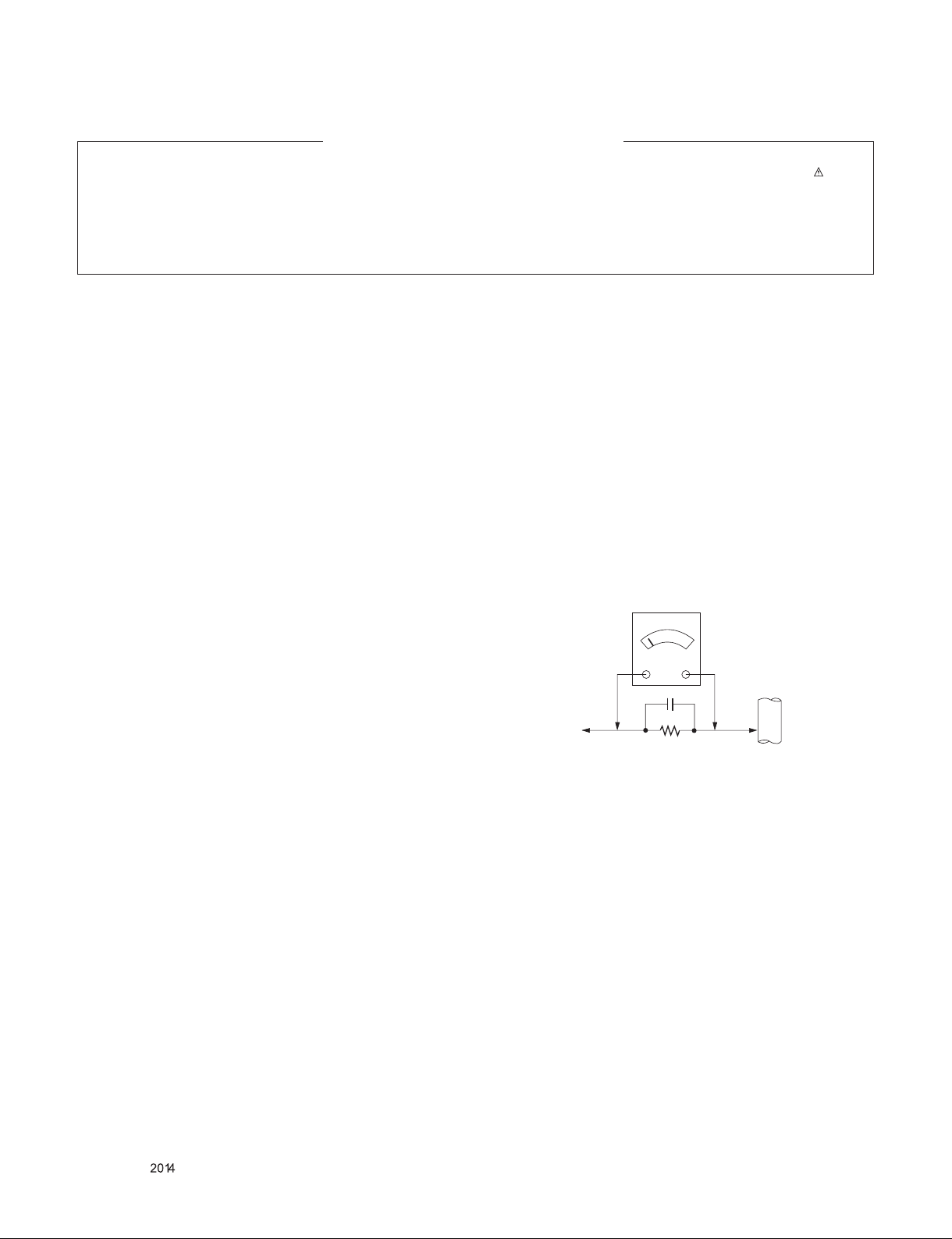
Leakage Current Hot Check (See below Figure)
Plug the AC cord directly into the AC outlet.
Do not use a line Isolation Transformer during this check.
Connect 1.5K/10watt resistor in parallel with a 0.15uF capacitor
between a known good earth ground (Water Pipe, Conduit, etc.)
and the exposed metallic parts.
Measure the AC voltage across the resistor using AC voltmeter
with 1000 ohms/volt or more sensitivity.
Reverse plug the AC cord into the AC outlet and repeat AC voltage
measurements for each exp ose d metallic par t. Any voltage
measured must not exceed 0.75 volt RMS which is corresponds to
0.5mA.
In case any measurement is out of the limits specified, there is
possibility of shock hazard and the set must be checked and
repaired before it is returned to the customer.
Leakage Current Hot Check circuit
Good Earth Ground
such as WATER PIPE,
To Instrument's
exposed
METALLIC PARTS
When 25A is impressed between Earth and 2nd Ground
for 1 second, Resistance must be less than 0.1
*Base on Adjustment standard
0.15µF
1.5 Kohm/10W
CONDUIT etc.
Copyright © LG Electronics. Inc. All right reserved.
Only for training and service purposes
- 3 -
LGE Internal Use Only

SERVICING PRECAUTIONS
CAUTION: Before servicing receivers covered by this service
manual and its supplements and addenda, read and follow the
SAFETY PRECAUTIONS on page 3 of this publication.
NOTE: If unforeseen circumstances create conflict between the
following servicing precautions and any of the safety precautions on
page 3 of this publication, always follow the safety precautions.
Remember: Safety First.
General Servicing Precautions
1. Always unplug the receiver AC power cord from the AC power
source before;
a. Removing or reinstalling any component, circuit board
module or any other receiver assembly.
b. Disconnecting or reconnecting any receiver electrical plug or
other electrical connection.
c. Connecting a test substitute in parallel with an electrolytic
capacitor in the receiver.
CAUTION: A wrong part substitution or incorrect polarity
installation of electrolytic capacitors may result in an
explosion hazard.
2. Test high voltage only by measuring it with an appropriate high
voltage meter or other voltage measuring device (DVM,
FETVOM, etc) equipped with a suitable high voltage probe.
Do not test high voltage by "drawing an arc".
3. Do not spray chemicals on or near this receiver or any of its
assemblies.
4. Unl ess sp ecified othe rwise in this service manua l, clean
electrical contacts only by applying the following mixture to the
contacts with a pipe cleaner, cotton-tipped stick or comparable
non-abrasive applicator; 10% (by volume) Acetone and 90% (by
volume) isopropyl alcohol (90%-99% strength)
CAUTION: This is a flammable mixture.
Unless specified otherwise in this service manual, lubrication of
contacts in not required.
5. Do not defeat any plug/socket B+ voltage interlocks with which
receivers covered by this service manual might be equipped.
6. Do not apply AC power to this instrument and/or any of its
electrical assemblies unless all solid-state device heat sinks are
correctly installed.
7. Always connect the test receiver ground lead to the receiver
chassis ground before connecting the test receiver positive
lead.
Always remove the test receiver ground lead last.
8. Use with this receiver only the test fixtures specified in this
service manual.
CAUTION: Do not connect the test fixture ground strap to any
heat sink in this receiver.
Electrostatically Sensitive (ES) Devices
Some semiconductor (solid-state) devices can be damaged easily
by static electricity. Such components com monly are called
Electrostatically Sensitive (ES) Devices. Examples of typical ES
devices are integrated circuits and some field-effect transistors and
semiconductor "chip" compon ents. The following techniques
should be used to help reduce the incide nce of component
damage caused by static by static electricity.
1. Immediately before handling any semiconductor component or
semiconductor-equipped assembly, drain off any electrostatic
charge on your body by touching a known earth ground.
Alter natively, obtain and wear a comme rcially availab le
discharging wrist strap device, which should be removed to
prevent potential shock reasons prior to applying power to the
unit under test.
2. After removing an electrical assembly equipped with ES
devices, place the assembly on a conductive surface such as
aluminum foil, to prevent electrostatic charge buildup or
exposure of the assembly.
3. Use only a grounded-tip soldering iron to solder or unsolder ES
devices.
4. Use only an anti-static type solder removal device. Some solder
removal devices not classified as "anti-static" can generate
electrical charges sufficient to damage ES devices.
5. Do not use freon-propelled chemicals. These can generate
electrical charges sufficient to damage ES devices.
6. Do not remove a replacement ES device from its protective
package until immediately before you are ready to install it.
(Most re pla cem ent ES dev ice s are packaged with leads
electrically shorted together by conductive foam, aluminum foil
or comparable conductive material).
7. Immediately before removing the protective material from the
leads of a replacement ES device, touch the protective material
to the chassis or circuit assembly into which the device will be
installed.
CAUTION: Be sure no power is applied to the chassis or circuit,
and observe all other safety precautions.
8. Mi nimiz e bodil y motions w hen h an dl ing u np ac kaged
replacement ES devices. (Otherwise harmless motion such as
the brushing together of your clothes fabric or the lifting of your
foot from a carp eted floor can ge ner ate st atic electricit y
sufficient to damage an ES device.)
General Soldering Guidelines
1. Use a grounded-tip, low-wattage soldering iron and appropriate
tip size and shape that will maintain tip temperature within the
range or 500 ˚F to 600 ˚F.
2. Use an appropriate gauge of RMA resin-core solder composed
of 60 parts tin/40 parts lead.
3. Keep the soldering iron tip clean and well tinned.
4. Thoroughly clean the surfaces to be soldered. Use a mall wirebristle (0.5 inch, or 1.25cm) brush with a metal handle.
Do not use freon-propelled spray-on cleaners.
5. Use the following unsoldering technique
a. Allow the soldering iron tip to reach normal temperature.
(500 ˚F to 600 ˚F)
b. Heat the component lead until the solder melts.
c. Quickly draw the melted solder with an anti-static, suction-
type solder removal device or with solder braid.
CAUTION: Work quickly to avoid overheating the circuit
board printed foil.
6. Use the following soldering technique.
a. Allow the soldering iron tip to reach a normal temperature
(500 ˚F to 600 ˚F)
b. First, hold the soldering iron tip and solder the strand against
the component lead until the solder melts.
c. Quickly move the soldering iron tip to the junction of the
component lead and the printed circuit foil, and hold it there
only un til the solder fl ows onto and around both the
component lead and the foil.
CAUTION: Work quickly to avoid overheating the circuit
board printed foil.
d. Closely inspect the solder area and remove any excess or
splashed solder with a small wire-bristle brush.
Copyright © LG Electronics. Inc. All right reserved.
Only for training and service purposes
- 4 -
LGE Internal Use Only

IC Remove/Replacement
Some chassis circuit boards have slotted holes (oblong) through
which the IC leads are inserted and then bent flat against the
circuit foil. When holes are the slotted type, the following technique
should be used to remove and replace the IC. When working with
boards using the familiar round hole, use the standard technique
as outlined in paragraphs 5 and 6 above.
Removal
1. Desolder and straighten each IC lead in one operation by gently
prying up on the lead with the soldering iron tip as the solder
melts.
2. Draw away the melted solder with an anti-static suction-type
solder removal device (or with solder braid) before removing the
IC.
Replacement
1. Carefully insert the replacement IC in the circuit board.
2. Carefully bend each IC lead against the circuit foil pad and
solder it.
3. Clean the soldered areas with a small wire-bristle brush.
(It is not necessary to reapply acrylic coating to the areas).
"Small-Signal" Discrete Transistor
Removal/Replacement
1. Remove the defective transistor by clipping its leads as close as
possible to the component body.
2. Bend into a "U" shape the end of each of three leads remaining
on the circuit board.
3. Bend into a "U" shape the replacement transistor leads.
4. Connect the replacement transistor leads to the corresponding
leads extending from the circuit board and crimp the "U" with
long nose pliers to insure metal to metal contact then solder
each connection.
CAUTION: Maintain original spacing between the replaced
component and adjacent components and the circuit board to
prevent excessive component temperatures.
Circuit Board Foil Repair
Excessive heat applied to the copper foil of any printed circuit
board will weaken the adhesive that bonds the foil to the circuit
board causing the foil to separate from or "lift-off" the board. The
following guidelines and procedures should be followed whenever
this condition is encountered.
At IC Connections
To repair a defective copper pattern at IC connections use the
following procedure to install a jumper wire on the copper pattern
si de of the circuit board. (Use this techniq ue onl y on IC
connections).
1. Carefully remove the damaged copper pattern with a sharp
knife. (Remove only as much copper as absolutely necessary).
2. carefully scratch away the solder resist and acrylic coating (if
used) from the end of the remaining copper pattern.
3. Bend a small "U" in one end of a small gauge jumper wire and
carefully crimp it around the IC pin. Solder the IC connection.
4. Route the jumper wire along the path of the out-away copper
pattern and let it overlap the previously scraped end of the good
copper pattern. Solder the overlapped area and clip off any
excess jumper wire.
At Other Connections
Use the following technique to repair the defective copper pattern
at connections other than IC Pins. This technique involves the
installation of a jumper wire on the component side of the circuit
board.
Power Output, Transistor Device
Removal/Replacement
1. Heat and remove all solder from around the transistor leads.
2. Remove the heat sink mounting screw (if so equipped).
3. Carefully remove the transistor from the heat sink of the circuit
board.
4. Insert new transistor in the circuit board.
5. Solder each transistor lead, and clip off excess lead.
6. Replace heat sink.
Diode Removal/Replacement
1. Remove defective diode by clipping its leads as close as
possible to diode body.
2. Bend the two remaining leads perpendicular y to the circuit
board.
3. Observing diode polarity, wrap each lead of the new diode
around the corresponding lead on the circuit board.
4. Securely crimp each connection and solder it.
5. Inspect (on the circuit board copper side) the solder joints of
the two "original" leads. If they are not shiny, reheat them and if
necessary, apply additional solder.
Fuse and Conventional Resistor
Removal/Replacement
1. Clip each fuse or resistor lead at top of the circuit board hollow
stake.
2. Securely crimp the leads of replacement component around
notch at stake top.
3. Solder the connections.
1. Remove the defective copper pattern with a sharp knife.
Remove at least 1/4 inch of copper, to ensure that a hazardous
condition will not exist if the jumper wire opens.
2. Trace along the copper pattern from both sides of the pattern
break an d loc ate the nearest component that is dir ect ly
connected to the affected copper pattern.
3. Connect insulated 20-gauge jumper wire from the lead of the
nearest component on one side of the pattern break to the lead
of the nearest component on the other side.
Carefully crimp and solder the connections.
CAUTION: Be sure the insulated jumper wire is dressed so the
it does not touch components or sharp edges.
Copyright © LG Electronics. Inc. All right reserved.
Only for training and service purposes
- 5 -
LGE Internal Use Only
SPECIFICATION
NOTE : Specications and others are subject to change without notice for improvement.
1. Application Range
This spec sheet is applied all of the TV used LM91X chassis.
2. Specication
Each part is tested as below without special appointment
1) Temperature : 25 ˚C ± 5 ˚C (77 ˚F ± 9 ˚F),
CST : 40 ˚C ± 5 ˚C
2) Relative Humidity : 65 % ± 10 %
3) Power Voltage : Standard input voltage
(100 V - 240 V ~, 50 / 60 Hz)
· Standard Voltage of each products is marked by models
4) Specication and performance of each parts are followed
each drawing and specication by part number in accordance with BOM.
5) The receiver must be operated for about 5 minutes prior to
the adjustment.
3.Test method
1) Performance : LGE TV test method followed
2) Demanded other specication
- Safety : CE,IEC specication
- EMC : CE,IEC specication
4. General specication
4.1. RGB-PC
No. Item Specication Remarks
1 Supported Sync. Type Separate Sync.(RGB), SOG
2 Operating Frequency Analog
3 Operating Frequency Analog
4 Operating Environment
5 Storage Environment
Temp : 10 °C ~ 35 °C
Humidity : 20 % ~ 80 %
Temp : -10 °C ~ 60 °C non condensing
Humidity : 5 % ~ 90 % non condensing
4.2. TV
No. Item Specication Remarks
1 Market Central and South America
2 Broadcasting system NTSC, PAL-M, PAL-N
BAND Available Channel
3 Available Channel
4 Receiving system Upper Heterodyne
5 Video Input PAL, SECAM, NTSC Rear (1EA)
6 RGB Input RGB-PC(Analog (D-SUB 15Pin) Rear (1EA)
7 USB Input MP3, JPEG, Movie Rear (1EA)
8 AV Audio Output RF/AV/HDMI Audio Output Rear (1EA)
9 HDMI Input HDMI-DTV Rear (1EA)
10 Audio Input (1EA) AV&RGB-PC L/R Input(1EA)
VHF
UHF
CATV
Horizontal 30 ~ 69 kHz
Vertical 56 ~ 61 Hz
Max 1366 × 768 @ 60 Hz
Recommend 1366 × 768 @ 60 Hz
02~13
14~69
02~125
Copyright ©
Only for training and service purposes
LG Electronics. Inc. All right reserved.
- 6 -
LGE Internal Use Only

5. RGB Input ( PC )
No. Resolution H-freq(kHz) V-freq.(Hz) Pixel clock(MHz) Proposed Remark
1 640*480 31.469 59.94 25.175
2 800*600 37.879 60.317 40.0
3 1024*768 48.363 60.0 65.0
4 1280*720 47.77 59.85 74.5
5 1152*864 54.34 60.05 80
6 1366*768 47.71 59.79 85.5
6. HDMI Input (DTV)
No Resolution H-freq(kHz) V-freq.(kHz) Pixel clock(MHz) Proposed Remarks
1 720*480 15.73 59.94 13.500 SDTV, DVD 480I(525I)
Spec. out but display.2 720*480 15.75 60.00 13.514 SDTV, DVD 480I(525I)
3 720*576 15.625 50.00 13.500 SDTV, DVD 576I(625I) 50Hz
4 720*480 31.47 59.94 27 SDTV 480P
5 720*480 31.5 60.00 27.027 SDTV 480P
6 720*576 31.25 50.00 27 SDTV 576P
7 1280*720 44.96 59.94 74.176 HDTV 720P
8 1280*720 45 60.00 74.25 HDTV 720P
9 1280*720 37.5 50.00 74.25 HDTV 720P
10 1920*1080 28.125 50.00 74.25 HDTV 1080I
11 1920*1080 33.72 59.94 74.176 HDTV 1080I
12 1920*1080 33.75 60.00 74.25 HDTV 1080I
13 1920*1080 56.25 50.00 148.5 HDTV 1080P
14 1920*1080 67.432 59.94 148.350 HDTV 1080P
15 1920*1080 67.5 60.00 148.5 HDTV 1080P
16 1920*1080 27 24.00 74.25 HDTV 1080P
17 1920*1080 33.75 30.00 74.25 HDTV 1080P
18 1920*1080 26.97 23.97 74.25 HDTV 1080P
19 1920*1080 33.716 29.976 74.25 HDTV 1080P
Copyright © LG Electronics. Inc. All right reserved.
Only for training and service purposes
- 7 -
LGE Internal Use Only

ADJUSTMENT INSTRUCTION
1. Application Range
This spec. sheet applies to LM91X Chassis applied TV all
models manufactured in TV factory
2. Specication
1) Because this is not a hot chassis, it is not necessary to
use an isolation transformer. However, the use of isolation
transformer will help protect test instrument.
2) Adjustment must be done in the correct order.
3) The adjustment must be performed in the circumstance of
25 °C ± 5 °C of temperature and 65 % ± 10 % of relative
humidity if there is no specic designation.
4) The input voltage of the receiver must keep AC 100-240
V~, 50/60 Hz.
5) The receiver must be operated for about 5 minutes prior to
the adjustment when module is in the circumstance of over
15. In case of keeping module is in the circumstance of 0
°C, it should be placed in the circumstance of above 15
°C for 2 hours. In case of keeping module is in the circumstance of below -20 °C, it should be placed in the circumstance of above 15 °C for 3 hours.
[Caution]
When still image is displayed for a period of 20 minutes or
longer (Especially where W/B scale is strong. Digital pattern
13ch and/or Cross hatch pattern 09ch), there can some afterimage in the black level area.
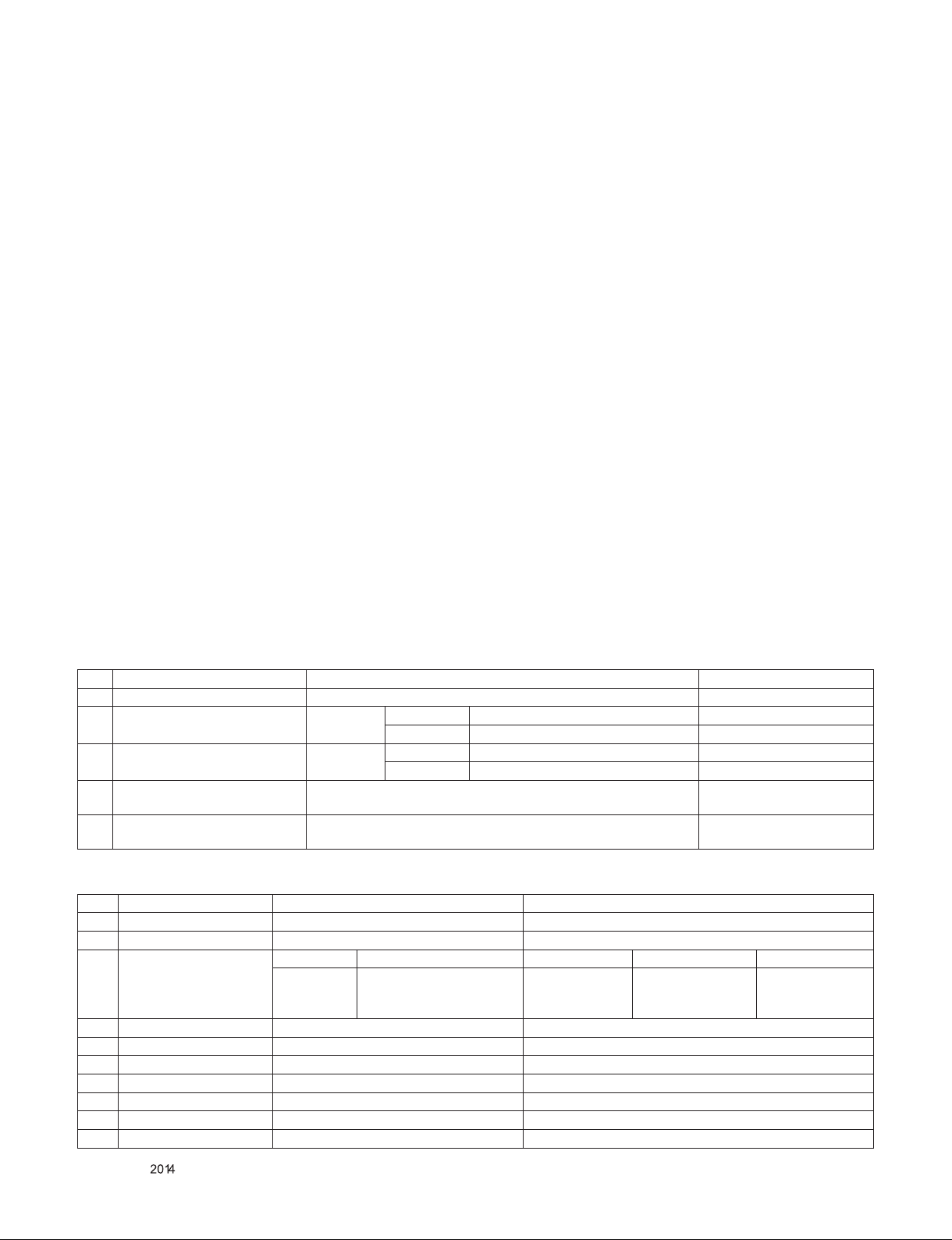
3. Main PCBA Adjustments
3.1. ADC Calibration
- An ADC calibration is automatically adjusted from DFT-Jig
- If it needs to adjust manually, refer to appendix.
NO Item CMD 1CMD 2Data 0
Enter
Adjust MODE
ADC
adjust
Adjust
‘Mode In’
ADC
adjust
A A 0 0 When transfer the
A D 1 0 Automatically adjustment
‘Mode In’,
Carry the command.
3.2.3. Download method
- The EDID data is automatically saved.
3.2.4. EDID DATA
- 29MT45A(RGB-PC)
** RGB-PC : 128Bytes
0 1 2 3 4 5 6 7 8 9 A B C D E F
0 00 FF FF FF FF FF FF 00 1E 6D C8 59 01 01 01 01
10 01 17 01 03 68 34 1D 78 EA 53 4D A3 56 4F 9E 26
20 0F 47 4A A1 08 00 01 40 45 40 61 40 71 40 81 00
30 81 C0 01 01 01 01 66 21 56 AA 51 00 1E 30 46 8F
40 33 00 3F 43 21 00 00 1E 00 00 00 FD 00 38 3D 1E
50 45 09 00 0A 20 20 20 20 20 20 00 00 00 FC 00 32
60 44 20 48 44 20 4C 47 20 54 56 0A 20 00 00 00 FF
70 00 0A 20 20 20 20 20 20 20 20 20 20 20 20 00 67
- 29MT45A(HDMI)
** HDMI : 256Bytes
0 1 2 3 4 5 6 7 8 9 A B C D E F
0 00 FF FF FF FF FF FF 00 1E 6D CA 59 01 01 01 01
10 01 17 01 03 80 34 1D 78 EA 53 4D A3 56 4F 9E 26
20 0F 47 4A 21 08 00 81 80 81 C0 71 40 B3 00 81 40
30 90 40 95 00 A9 C0 66 21 56 AA 51 00 1E 30 46 8F
40 33 00 09 25 21 00 00 1A 02 3A 80 18 71 38 2D 40
50 58 2C 45 00 09 25 21 00 00 1E 00 00 00 FD 00 38
60 3D 1E 45 0F 00 0A 20 20 20 20 20 20 00 00 00 FC
70 00 32 44 20 48 44 20 4C 47 20 54 56 0A 20 01 30
80 02 03 21 F1 4F 84 05 03 02 20 22 10 11 13 12 14
90 1F 07 16 01 26 11 07 50 09 7F 07 65 03 0C 00 10
A0 00 02 3A 80 18 71 38 2D 40 58 2C 45 00 09 25 21
B0 00 00 1A 01 1D 80 18 71 1C 16 20 58 2C 25 00 09
C0 25 21 00 00 9E 01 1D 00 72 51 D0 1E 20 6E 28 55
D0 00 09 25 21 00 00 1E 01 1D 80 D0 72 1C 16 20 10
E0 2C 25 80 09 25 21 00 00 9E 02 3A 80 D0 72 38 2D
F0 40 10 2C 45 20 09 25 21 00 00 1E 00 00 00 00 6F
* ADC Calibration Protocol (RS-232)
Adjust Sequence
▪aa 00 00 [Enter Adjust Mode]
▪xb 00 60 [RGB Input (1024*768)]
▪ad 00 10 [Adjust 1024*768 RGB]
▪aa 00 90 End Adjust mode
3.2. EDID Download
3.2.1. Overview
- It is a VESA regulation. A PC or a MNT will display an
optimal resolution through information sharing without any
necessity of user input. It is a realization of “Plug and Play”.
3.2.2. Equipment
- Since EDID data is embedded, EDID download JIG, HDMI
cable and D-sub cable are not need.
Copyright © LG Electronics. Inc. All right reserved.
Only for training and service purposes
- 8 -
LGE Internal Use Only

4. Final Assembly Adjustment
4.1. White Balance Adjustment
4.1.1. Overview
▪ W/B adj. Objective & How-it-works
(1) Objective: To reduce each Panel's W/B deviation
(2) How-it-works : When R/G/B gain in the OSD is at 192, it
means the panel is at its Full Dynamic Range. In order to
prevent saturation of Full Dynamic range and data, one of
R/G/B is xed at 192, and the other two is lowered to nd
the desired value.
(3) Adjustment condition : normal temperature
1) Surrounding Temperature : 25 °C ± 5 °C
2) Warm-up time: About 5 Min
3) Surrounding Humidity : 20 % ~ 80 %
4) Before White balance adjustment, Keep power on
status, don’t power off
* Adj. condition and cautionary items
(1) Lighting condition in surrounding area surrounding lighting
should be lower 10 lux. Try to isolate adj. area into dark
surrounding.
(2) Probe location: Color Analyzer (CA-210) probe should
be within 10cm and perpendicular of the module surface
(80°~ 100°)
(3) Aging time
1) After Aging Start, Keep the Power ON status during
5 Minutes.
2) In case of LCD, Back-light on should be checked
using no signal or Full-white pattern.
4.1.2. Equipment
(1) Color Analyzer: CA-210 (NCG: CH 9 / WCG: CH12 / LED:
CH14)
(2) Adj. Computer (During auto adj., RS-232C protocol is
needed)
(3) Adjust Remocon
(4) Video Signal Generator MSPG-925F 720p/204-
Gray(Model: 217, Pattern: 49)
* Color Analyzer Matrix should be calibrated using CS-1000
4.1.4. Adjustment Command (Protocol)
(1) RS-232C Command used during auto-adj.
RS-232C COMMAND
CMD ID DATA
wb 00 00 Begin White Balance adjustment
wb 00 ff
End White Balance adjustment
(internal pattern disappears )
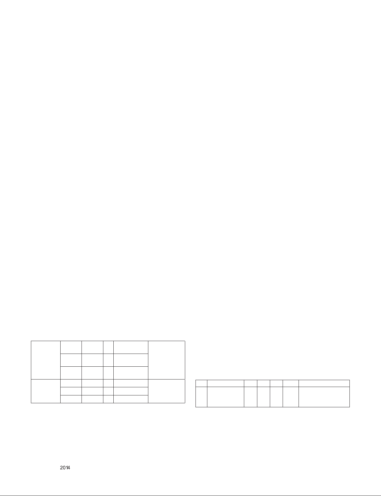
(2) Adjustment Map
Command
(lower caseASCII)
CMD1 CMD2 MIN MAX
Cool
Medium
Warm
Adj. item
R Gain j g 00 C0
G Gain j h 00 C0
B Gain j i 00 C0
R Cut
G Cut
B Cut
R Gain j a 00 C0
G Gain j b 00 C0
B Gain j c 00 C0
R Cut
G Cut
B Cut
R Gain j d 00 C0
G Gain j e 00 C0
B Gain j f 00 C0
R Cut
G Cut
Explantion
Data Range
(Hex.)
Default
(Decimal)
4.1.3. Equipment connection
Co lor Ana ly ze r
Pro be
DFT JIG
RRGB Cabl e S -23 2C
Signal S ourc e
* If TV internal pattern is used, not needed
Copyright © LG Electronics. Inc. All right reserved.
Only for training and service purposes
Co m pu ter
Patt er n G en erat or
RS-23 2C
RS-23 2C
- 9 -
LGE Internal Use Only
4.1.5. Adj. method
*Auto WB calibration
1) Set TV in ADJ mode using P-ONLY key (or POWER ON
key)
2) Place optical probe on the center of the display
- It need to check probe condition of zero calibration
before adjustment.
3) Connect RS-232C Cable
4) Select mode in ADJ Program and begin a adjustment.
5) When WB adjustment is completed with OK message,
check adjustment status of pre-set mode (Cool, Medium,
Warm)
6) Remove probe and RS-232C cable.
▪ W/B Adj. must begin as start command “wb 00 00” , and n-
ish as end command “wb 00 ff”, and Adj. offset if need.
* LED White balance table
If Model is Polaris Model, G-gain x is applied.
(1) Cool Mode
1) Purpose : Especially G-gain x adjust leads to the lu-
minance enhancement. Adjust the color temperature
to reduce the deviation of the module color temperature.
2) Principle : To adjust the white balance without the
saturation, Adjust the G gain more than 172 ( If R
gain or G gain is more than 255 , G gain can adjust
less than 172 ) and change the others ( R/B Gain ).
3) Adjustment mode : mode – Cool
(2) Medium / Warm Mode
1) Purpose : Adjust the color temperature to reduce the
deviation of the module color temperature.
2) Principle : To adjust the white balance without the
saturation, Fix the one of R/G/B gain to 192 (default
data) and decrease the others.
3)Adjustment mode : Two modes – Medium / Warm
4.1.6 Reference
(White Balance Adj. coordinate and color temperature)
1) Luminance: 204 Gray, 80IRE
2) Standard color coordinate and temperature using CS-1000
(over 26 inch)
4.1.7. Reference
(White Balance Adj. coordinate and color temperature)
* The spec of color temperature and coordinate.
Color
Temperature
Luminance
(cd/m²)
*Note : x,y coordinates are drifted about 0.007 after 30 mins
heat-run. So checking color coordinate within 5-min at total
assembly line, consider x,y coordinates might be up to 0.007
than x,y target of each color temperature.
Cool 9,300k °K X=0.274 (±0.03)
Medium 8,000k °K X=0.290 (±0.03)
Warm 6,500k °K X=0.318 (±0.03)
Cool Min : 80 Typ : 110 <Test Signal>
Medium Min : 80 Typ : 110
Warm Min : 70 Typ : 110
Y=0.278 (±0.03)
Y=0.298 (±0.03)
Y=0.334 (±0.03)
<Test Signal>
- Inner pattern
for W/B adjust
- External white
pattern
(80IRE, 204gray)
Inner pattern
(204gray,80IRE)
5. Tool Option selection
▪ Method : Press "ADJ" key on the Adjustment remote control,
then select Tool option.
6. Ship-out mode check(In-stop)
▪ After nal inspection, press "IN-STOP" key of the Adjustment
remote control and check that the unit goes to Stand-by
mode.
7. GND and Hi-pot
7.1. GND & HI-POT auto-check preparation
1) Check the POWER CABLE and SIGNAL CABE insertion
condition
7.2. GND & HI-POT auto-check
1) Pallet moves in the station. (POWER CORD / AV CORD is
tightly inserted)
2) Connect the AV JACK Tester.
3) Controller (GWS103-4) on.
4) GND Test (Auto)
- If Test is failed, Buzzer operates.
- If Test is passed, execute next process (Hi-pot test).
(Remove A/V CORD from A/V JACK BOX)
5) HI-POT test (Auto)
- If Test is failed, Buzzer operates.
- If Test is passed, GOOD Lamp on and move to next
process automatically.
7.3. Checkpoint
1) Test voltage
- GND: 1.5KV/min at 100mA
- SIGNAL: 3KV/min at 100mA
2) TEST time: 1 second
3) TEST POINT
- GND Test = POWER CORD GND and SIGNAL CA-
BLE GND.
- Hi-pot Test = POWER CORD GND and LIVE & NEU-
TRAL.
4) LEAKAGE CURRENT: At 0.5mArms
8. Audio
Measurement condition:
1) RF input: Mono, 1 KHz sine wave signal, 100 % Modulation
2) CVBS, Component: 1 KHz sine wave signal 0.5 Vrms
3) RGB PC: 1 KHz sine wave signal 0.7 Vrms
No. Item Min Typ Max Unit Remark
Audio practical
max Output, L/R
1
(Distortion=10%
max Output)
4.5 5.0 6.0WVrms
(1) Measurement condition
- EQ/AVL/Clear Voice: Off
(2) Speaker(8Ω Impedance)
Copyright © LG Electronics. Inc. All right reserved.
Only for training and service purposes
- 10 -
LGE Internal Use Only
 Loading...