

Page 1

North/Latin America http://aic.lgservice.com
Europe/Africa http://eic.lgservice.com
Asia/Oceania http://biz.lgservice.com
LED LCD TV
サービスマニュアル
CHASSIS : LE22A
MODEL : 22LS3500 22LS3500-JB
CAUTION
BEFORE SERVICING THE CHASSIS,
READ THE SAFETY PRECAUTIONS IN THIS MANUAL.
Internal Use Only
Printed in KoreaP/NO : MFL67469505 (1205-REV00)
Page 2

目 次
目次 ........................................................................................................................................ 2
安全上の注意事項 ............................................................................................................. 3
サービス上の注意事項 ..................................................................................................... 4
仕様 ......................................................................................................................................... 6
調整方法 .................................................................................................................................9
分解図 .................................................................................................................................. 20
サービスシート ......................................................................................................................
Only for training and service purposes
- 2 -
LGE Internal Use OnlyCopyright © LG Electronics. Inc. All rights reserved.
Page 3
安全上の注意事項
重要安全指示事項
この製品には、安全に関連して重要な特性を持つ電気部品と機械部品が数多く使用されています。これらの部品は、回路図上および「交換部品
の一覧表」では で示されています。
X 線被曝、感電、火災などの危険を防止するために、これらの重要部品を交換する際は、このマニュアルで推奨しているとおりの部品と交換す
る必要があります。
製造元の承認を得ずに元の設計を改変しないでください。
一般的なガイドライン
AC 電源から絶縁されていないシャーシを持つ受信機をサービスする
際は、必ず絶縁トランスを使用する必要があります。絶縁トランスには
十分な電力定格を持つものを使用してください。これにより、作業者が
感電によってけがを負う事故を防止できます。
また、サービス作業中に不注意で回路を短絡させた場合でも、絶縁ト
ランスを使用していれば、受信機とその内部部品を保護できます。
このテレビ受信機のヒューズ(またはヒューズ抵抗) が飛んでいる場合
は、指定どおりのヒューズ(またはヒューズ抵抗) と交換してください。
定格電力が大きい抵抗(1 W を超える酸化金属被膜抵抗) を交換する
場合は、抵抗本体とプリント基板との間に10 mm 以上の空間が確保
されるように実装してください。
内部配線材は、高圧部品や高温部品から離して引き回してください。
受信機をユーザーに返却する前に,
必ず、受信機筐体の露出金属部(アンテナ、端子類、など) からのAC 漏
洩電流値を確認し、その受信機を使用しても感電の危険がないことを
確認してください。
非通電での漏洩電流確認(アンテナコールド側での確認) 製品のAC プ
ラグをコンセントから抜き、AC プラグの端子間をジャンパ線で短絡し
ます。製品の電源スイッチをオン位置にして、ジャンパ線で短絡した
AC プラグの端子に抵抗計の一方の測定リードを接続します。他方の
測定リードを、アンテナ端子やヘッドホンジャックなどの露出金属部
に順番に接触させて抵抗値を測定します。
露出金属部とシャーシとの間に帰路抵抗器が存在する場合、抵抗計の
指示は1 ~ 5.2 MΩの範囲となります。 この帰路抵抗器が存在しない
場合、抵抗計の指示は無限大です。 なんらかの異常が認められた場
合は、受信機をユーザーに返却する前に、その異常を修復する必要が
あります。
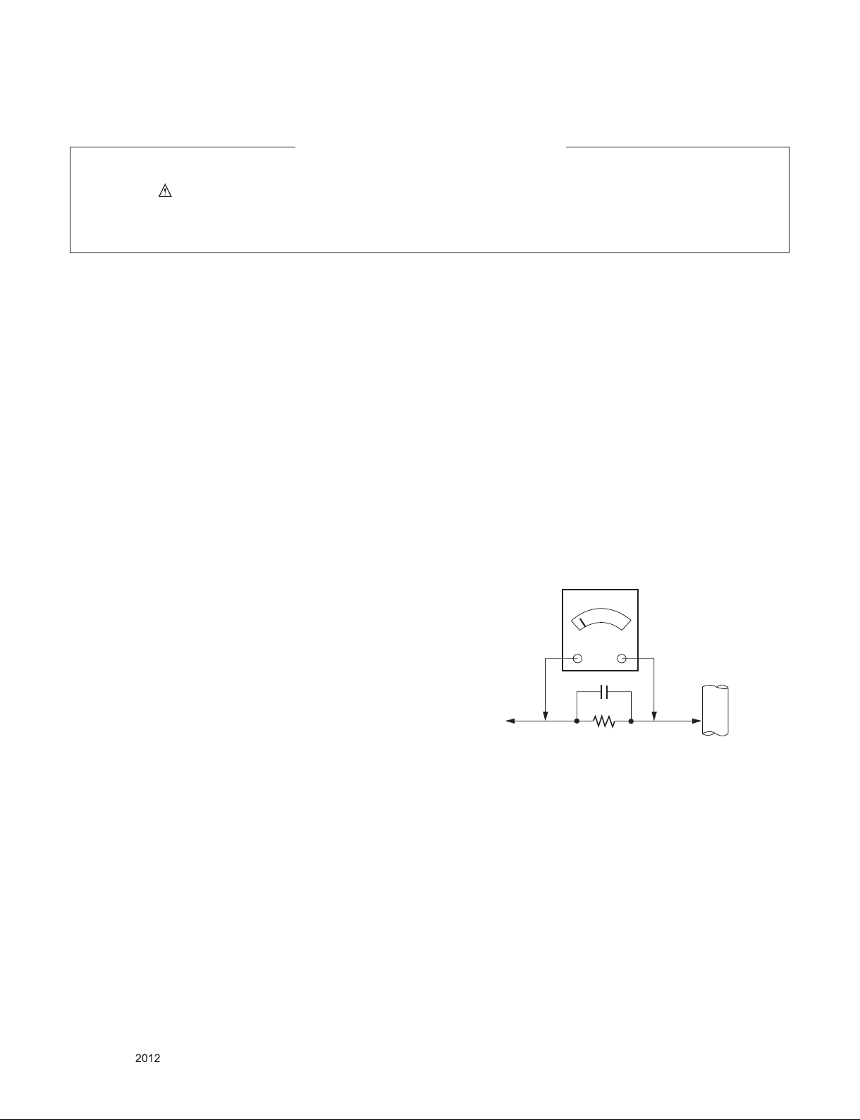
通電状態での漏洩電流確認(下図を参照)
製品のAC プラグをコンセントに直接差し込みます。
この確認作業では、電源絶縁トランスを使用しないでください。
0.15 uF のコンデンサと並列に接続した1.5 kΩ/10 W の抵抗を、良好
な接地状態にあることがわかっている部分(水道管、コンジットなど)
と、製品の露出金属部との間に接続します。
1000 Ω/V以上の感度を持つAC 電圧計で、抵抗両端のAC 電圧
を測定します。
コンセントに対するAC プラグの差し込み極性を逆にして、上記
同様に露出金属部について抵抗両端のAC 電圧を測定します。
どの場合であっても、抵抗両端の電圧は0.75 Vrms (漏洩電流
0.5 mA) 以下であることが必要です。
測定値が上記の限度値を超過する場合、その製品には感電の危
険があるので、ユーザーに返却する前に原因を特定して限度値
以下となるように修復する必要があります。
通電状態で漏洩電流を確認するための回路
AC 電圧計
水道管、コンジット
製品の露
出金属部へ
0.15uF
1.5 kΩ/10W
などの良好な接地部
Only for training and service purposes
- 3 -
LGE Internal Use OnlyCopyright © LG Electronics. Inc. All rights reserved.
Page 4

サービス上の注意事項
注意: このサービスマニュアルおよびその付録、追加版で説明している
受信機のサービスを進める前に、この文書の3 ページにある「安全上
の注意事項」に目を通し、サービスはその指示に従ってください。
注: 予期せぬ状況により、以下に記されているサービス上の注意事項
と、この文書の3 ページにある「安全上の注意事項」とが矛盾する場合
は、必ず「安全上の注意事項」に従ってください。 安全第一を心がけて
ください。
サービス上の一般的な注意事項
1. 以下の作業を進める前に、受信機のAC プラグを必ずコンセントか
ら抜いてください。
a. 部品やプリント基板モジュールなどの受信機アセンブリを取り外
すとき、またはそれらを取り付けるとき
b. 受信機の電気的コネクタを取り外すとき、または接続し直すとき
c. 受信機の電解コンデンサと並列にテスト用の代替品を接続する
とき
注意 : 解コンデンサは、定格が異なるものに交換したり、逆極性で
実装したりすると、破裂するおそれがあります。
2. 高電圧の試験では、高電圧プローブを備えた適切な高電圧計また
は電圧測定装置(デジタル電圧計、FET 入力型電圧計など) のみを使
用してください。
放電によるアークを確認することで高電圧をテストしないでくださ
い。
3. この受信機またはそのアセンブリ自体に、またはその近くで化学薬
品をスプレーしないでください。
4. このサービスマニュアルに別途記載がない限り、電気接点の清掃に
は、アセトンとイソプロピルアルコール(純度90 ~ 99%) を体積比
10:90 で混ぜた液で湿らせたパイプクリーナー、綿棒など表面の柔
らかいものを使用します。
注意 : の液は可燃性です。
このサービスマニュアルに別途記載がない限り、接点の潤滑は不要
です。
5. このサービスマニュアルで説明している受信機は、プラグやソケット
のB+ 電圧インターロック機能を備えてい ることがあります。このイ
ンターロック機能は無効にしないでください。
6. 半導体部品の放熱器をすべて正しく取り付けていない限り、製品や
その電気アセンブリに通電しないでください。
7. テスト用受信機の正側のリードを接続する前に、テスト受信機のグ
ランドリードを必ず受信機のシャーシグランドに接続してください。
取り外しの際は、テスト用受信機のグランドリードを必ず最後に取り
外してください。
8. このサービスマニュアルで指定しているテスト装置は、この受信機
専用です。
注意 : テスト装置のグランドストラップを、この受信機内部の放熱器
には接続しないでください。
静電気に敏感な(ES) 部品
半導体部品によっては、静電気で容易に破壊されるものがあります。こ
のような部品を、静電気に敏感な(ES) 部品と呼んでいます。典型的な
ES 部品として、集積回路、一部の電界効果トランジスタ、半導体チップ
部品があります。部品の静電気破壊を低減する上で、次に挙げる手法
が役に立ちます。
1. 半導体部品や半導体を使用したアセンブリを扱う直前に、接地され
ていることがわかっている部分に触れて体内に蓄積されている静電
気を放電させます。
または、市販の放電用リストストラップを装着します。感電の危険を
防止するために、テスト中に製品などに通電する場合は、このストラ
ップは外してください。
2. ES 部品を使用した電気系アセンブリを取り外した後、それをアルミ
ホイルのような導電性の表面上に置きます。これにより、静電荷の蓄
積が発生せず、静電気にさらされることもなくなります。
3. ES 部品のはんだ付けやはんだ除去には、こて先が接地されている
はんだごてを使用します。
4. はんだ除去工具には、静電気防止型を使用します。はんだ除去工具
によっては、静電気防止型ではないものがあります。このような工具
を使用すると、ES 部品を破壊する量の電荷が生成されることがあり
ます。
5. フレオンを使用したスプレー薬品は使用しないでください。ES 部品
を破壊する量の電荷が生成されることがあります。
6. 交換用のES 部品は、保護パッケージから取り出した後、直ちに実装
してください
(ほとんどの交換用ES 部品は、そのリード部分が導電性スポンジ、ア
ルミホイル、または同等の導電性保護材に差し込まれ、すべてのリ
ードが短絡された状態で梱包されています)。
7. 保護材から交換用ES 部品を抜き取る直前に、その部品の実装先で
あるシャーシや回路アセンブリに保護材を接触させます。
注意 : シャーシや回路に通電していないことを確認し、すべての安
全上の注意事項に従ってください。
8. 交換用ES 部品が梱包されているパッケージを扱う際は、体の大き
な動きを避けてください(衣服の繊維どうしをこすり合わせたり、足
をカーペットの床から上げたりするような動作により、ES 部品を破
壊する量の電荷が生成されることがあります)。
はんだ付けの一般的なガイドライン
1. こて先が接地される形式の小電力はんだごてを使用し、こて先温度
を260 ~ 310 ℃に保持する上で適切な大きさと形状のこて先を装
着します。
2. 適切な径を持ち、スズ60%、鉛40% で構成される、RMA フラックス入
りはんだを使用します。
3. こて先は常に清掃し、つやがあるようにします。
4. はんだ付けする表面を十分に清掃してください。清掃には、金属製
の柄が付いた1.25 cm の豚毛ブラシを使用します。
フレオンを使用したスプレー式洗浄は使用しないでください
5. はんだの除去は、次の方法に従ってください。
a. こて先の温度が適正な温度(260 ~ 310 ℃) になるようにします。
b. はんだが溶けるまで部品のリードをはんだごてで加熱します。
c. 静電気防止型の吸い取り式はんだ除去工具、またははんだ吸着
リボンを使用して、溶けたはんだをすばやく吸い取ります。
注意 : プリント基板の銅箔が過熱しないように、手早く作業してくだ
さい。
6. はんだ付けは、次の方法に従ってください。
a. こて先の温度が適正な温度(260 ~ 310 ℃) になるようにします。
b. まず、はんだごてを持ち、こて先を部品のリードに当てて、そこで
はんだを溶かします。
C. はんだが溶けたら、すぐにこて先を部品リードがプリント基板の
銅箔に接している位置まで動かして、その位置でしばらく保持し
ます。部品リードと銅箔の両方に溶けたはんだが流れたら、すぐ
にこて先を離します。
注意 : プリント基板の銅箔が過熱しないように、手早く作業してくだ
さい。
d. はんだ付けした周辺を注意深く検査し、余分なはんだや飛散し
たはんだがあれば、小型の豚毛ブラシで取り除きます。
Only for training and service purposes
- 4 -
LGE Internal Use OnlyCopyright © LG Electronics. Inc. All rights reserved.
Page 5

IC の取り外しと交換
IC のリードを差し込むためにスロット状(長方形) の孔があいているプ
リント基板があります。このような孔に差し込まれたリードは、銅箔面
側で銅箔に沿って平らに折り曲げられています。このようなスロット状
の孔を使用しているIC の場合、その取り外しと交換は次の手順に従っ
てください。リードを差し込む孔が通常の円形となっているプリント基
板の場合は、前記の手順5 と6 に従ってください。
取り外し
1. はんだごてでIC のリードのはんだを溶かします。はんだが溶けてい
る間に、折れ曲がっているリードをこて先で注意深く起こして、リード
をまっすぐにします。この作業を、IC のすべてのリードで行います。
2. 静電気防止型の吸い取り式はんだ除去工具、またははんだ吸着リ
ボンを使用して、溶けたはんだを吸い取った後、IC を取り外しま
す。Replacement
1. 交換用IC をプリント基板に差し込みます。
2. IC の各リードがプリント基板の銅箔に沿うようにゆっくりと折り曲
げ、はんだ付けします。
3. 小型の豚毛ブラシではんだ付け周辺を清掃します
(はんだ付け周辺をアクリルコーティングし直す必要はありません)。
小信号ディスクリートトランジスタの取り外しと交換
Removal/Replacement
1. 動作不良になったトランジスタは、トランジスタ本体にできる限り近
い位置ですべてのリードを切断して取り除きます。
2. プリント基板上に残った
3. 交換用トランジスタのリードの先端をU 字状に曲げます。
4. 交換用トランジスタのリードと、プリント基板上でそのリードに相当
するリードとをU 字状部分で接続します。次に、ラジオペンチの先端
でそのU 字状部分をつぶし、リードどうしがしっかり接触するように
してはんだ付けします。
電力出力トランジスタの取り外しと交換
Removal/Replacement
1. トランジスタのリード周囲のはんだを加熱して溶かし、取り除きま
す。
2. 放熱器の取り付けねじがある場合は、そのねじを取り外します。
3. プリント基板上の放熱器からトランジスタを注意深く取り外します。
4. 新しいトランジスタをプリント基板の取り付け孔に差し込みます。
5. トランジスタの各リードをはんだ付けし、リードの余分な部分を切り
取ります。
6. トランジスタを放熱器に取り付け直します。
ダイオードの取り外しと交換
1. 動作不良になったダイオードは、ダイオード本体にできる限り近い
位置ですべてのリードを切断して取り除きます。
2. プリント基板に残った2 本のリードを、プリント基板に対して垂直に
曲げ伸ばします。
3. ダイオードの極性に注意して、新しいダイオードのリードを、プリント
基板上でそのリードに相当するリードに巻き付けます。
4. 巻き付けた部分をつぶして確実に接触するようにした後、はんだ付
けします。
5. プリント基板の銅箔面側を検査して、元からあるリードが確実には
んだ付けされていることを確認します。はんだ表面に輝きがない場
合は、はんだを加熱していったん溶かし、はんだ付けし直します。必
要に応じて、はんだを追加してください。
ヒューズおよび通常の形式の抵抗の取り外しと交換
Removal/Replacement
1. ヒューズや抵抗のリードを、プリント基板上の中空上の支柱の上部
で切断します。
2. 交換用部品のリードを支柱上部の切り込みにしっかりと巻き付けま
す。
3. 接続部をはんだ付けします。
注意 : 部品の過熱を防止するために、交換部品と周囲の部品との空
間距離、および交換部品とプリント基板との空間距離は、部品
交換前の距離を維持するようにしてください。
プリント基板銅箔パターンの修復
プリント基板の銅箔に過度の熱を加えると、銅箔をプリント基板の基
材に固定している接着剤が劣化して、銅箔が剥離したり、基材から浮き
上がったりします。そのような状況になった場合は、以下のガイドライ
ンと手順に従ってください。
IC 接続部
IC 接続部の銅箔パターンの損傷を修復するには、以下の手順に従って
プリント基板の銅箔パターン側にジャンパ線をはんだ付けします(この
手順は、IC 接続部のみに適用してください)。
1. 鋭いナイフを使用して、損傷した銅箔パターンを切り取って取り除き
ます(損傷している最小限の銅箔のみを取り除くようにしてください)。
2. 残った銅箔パターンの端部から、はんだレジストを掻き取ります。ア
クリルコーティングが施されている場合は、それも取り除きます。
3. 径の細いジャンパ線の一端をU 字状に曲げ、そのU 字部をIC のピ
ンに差し込んで注意深くつぶします。このIC とジャンパ線の接続部
をはんだ付けします。
4. 取り除いた銅箔パターンと同じ経路が形成されるように、残ってい
る銅箔のはんだレジストを除去した部分までジャンパ線を曲げて配
線し、銅箔部分にジャンパ線を重ねます。この重ねた部分ではんだ
付けして、余分なジャンパ線を切り取ります。
IC 以外の部品の接続部
IC のピン以外の接続部で損傷した銅箔パターンを修復するには、以下
の手順に従ってください。この手順では、プリント基板の部品面側にジ
ャンパ線を追加します。
1. 鋭いナイフを使用して、損傷した銅箔パターンを切り取って取り
除きます。
ジャンパ線が外れても危険な状況にならないように、銅箔は6.4
mm 以上取り除きます。
2. 取り除いた銅箔パターン部分の両側からパターンを追跡し、残っ
た銅箔パターンに接続されていて、最も近い位置にある部品を
それぞれの側で探し出します。
3. 線径AWG20 の絶縁被覆付きジャンパ線で、これら2 つの部品の
リードどうしを接続します。
ジャンパ線を部品のリードに巻き付けてしっかり固定し、はんだ
付けします。
注意 : この絶縁被覆付きジャンパ線は、部品や鋭い縁に接触しな
いように引き回してください。
Only for training and service purposes
- 5 -
LGE Internal Use OnlyCopyright © LG Electronics. Inc. All rights reserved.
Page 6
仕 様
注: 仕様を初めとする情報は、性能改善などのために予告なく変更されることがあります。
1. 適用範囲
この仕様書は、22/26/32 LCD TVで使用されるLE22A/Bシャーシ
に適用されます。
2. 仕様
特記なき限り、各部品は以下の条件でテストされています。
2.1. 温度 : 25 ± 5 ℃(77 ± 9 ℉)、CST : 40 ± 5 ℃
2.2. 相対湿度 : 65 ± 10%
2.3. 電源電圧 : 標準入力電圧(100 V以上、50/60 Hz)
▪ 各製品の標準電圧はモデル別に記載しています。
2.4. 各部品の仕様と性能に続いて、部品表に従って品番を記載し
ています。
2.5. 調整前に受像機を約5分間操作する必要があります。
3. テスト方法
3.1. 性能 : LGE TV テスト方法に準拠
3.2. 必要な他の仕様
安全:JQA仕様
EMC:JQA
4. 電気的仕様
4.1. 全般仕様
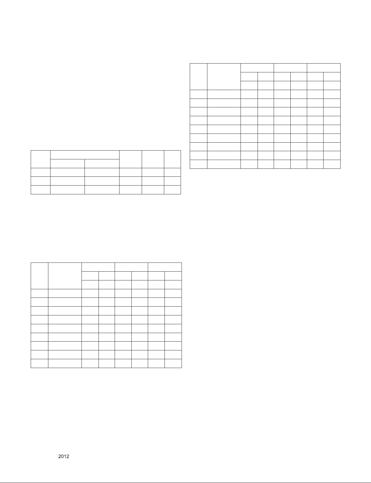
番号 項目 仕様 備考
1 ディスプレイ画面デバイス 32インチ カラー ディスプレイ モジュール 解像度:1366*768
26インチ カラー ディスプレイ モジュール 解像度:1366*768
22インチ カラー ディスプレイ モジュール 解像度:1366*768
2. 画面サイズ 16:9
3. LCDモジュール 32インチ60Hz HD Edge LED (LC320EXN-SEA2) 32LS3500/32LS3590
26インチ60Hz HD Edge LED (LC260EXN-SDA1) 26LS3500
22インチ60Hz HD Edge LED (V216BG1-LE1) 22LS3500 (CMI)
4. 使用環境 1) 温度 :0~40°
2) 湿度:0~80%
5. 保管環境 1) 温度 :-20~60°
2) 湿度:0~85 %
6 入力電圧 AC100~120 V、50/60 Hz
7 消費電力
=LCD(モジュール)+
バックライト(LED)
8 LCDモジュール 大きさ メーカー インチ (H)×(V)×(D) 単位:mm
ピクセル ピッチLGD 32インチ 0.51075 x 0.17025 LC320EXN-SEA2,
32インチ 60Hz HD Edge LED 32LS3500/32LS3590
26インチ 60Hz HD Edge LED 26LS3500
22インチ 60Hz HD Edge LED 22LS3500 (CMI)
LGD 32インチ 735.4 x 433.0 x 10.8 LC320EXN-SEA2,
32LS3590/32LS3500
26インチ 609.8 x 357.8 x 14.6 LC260EXN-SDA1,
26LS3500
22インチ
26インチ 0.4215 × 0.1405 LC260EXN-SDA1,
22インチ 0.1165 x 0.3495 V216BG1-LE1, 22LS3500
501 × 297 × 11.2
V216BG1-LE1, 22LS3500
32LS3590/32LS3500
26LS3500
Only for training and service purposes
- 6 -
LGE Internal Use OnlyCopyright © LG Electronics. Inc. All rights reserved.
Page 7
番号 項目 仕様 備考
バックライト LGD 32インチ エッジLED LC320EXN-SEA2,
32LS3590/32LS3500
26インチ エッジLED LC260EXN-SDA1,
26LS3500
22インチ エッジLED V216BG1-LE1, 22LS3500
ディスプレイ カラー 16.7 M(8ビット) FHD 60 Hzモデルを除く
コーティング 3H(ハード コーティング)、アンチグレア
5. 外部入力サポート形式
5.1. D5ビデオ入力(Y、PB、PR)
番号 解像度
1. 720*480 15.73 59.94 13.500 SDTV, DVD 480I(525I)
2 720*480 15.75 60.00 13.514 SDTV, DVD 480I(525I)
3 720*480 31.47 59.94 27.000 SDTV 480P
4 720*480 31.50 60.00 27.027 SDTV 480P
5 1280*720 44.96 59.94 74.176 HDTV 720P
6 1280*720 45.00 60.00 74.250 HDTV 720P
7 1920*1080 33.72 59.94 74.176 HDTV 1080I
8 1920*1080 33.75 60.00 74.25 HDTV 1080I
9 1920*1080 67.432 59.94 148.350 HDTV 1080P
10 1920*1080 67.5 60.00 148.5 HDTV 1080P
水平周波数
(kHz)
垂直周波数
(Hz)
ピクセル クロック
(MHz)
推奨 備考
5.2. RGB入力(PC)
番号 解像度
1. 640*350 31.468 70.09 25.17 EGA
2 720*400 31.469 70.08 28.32 DOS
3 640*480 31.469 59.94 25.17 VESA(VGA)
4 800*600 37.879 60.317 40 VESA(SVGA)
5 1024*768 48.363 60.004 65 VESA(XGA)
6 1152*864 54.348 60.053 80.002 VESA
水平周波数
(kHz)
垂直周波数
(Hz)
ピクセル クロック
(MHz)
推奨 備考
Only for training and service purposes
- 7 -
LGE Internal Use OnlyCopyright © LG Electronics. Inc. All rights reserved.
Page 8
5.3. HDMI入力
5.3.1. DTVモード
番号 解像度
1 720*480 15.73 59.94 13.500 SDTV, DVD 480I(525I) 仕様外 であるが
2 720*480 15.75 60.00 13.514 SDTV, DVD 480I(525I)
3 720*480 31.47 59.94 27 SDTV 480P
4 720*480 31.5 60.00 27.027 SDTV 480P
5 1280*720 44.96 59.94 74.176 HDTV 720P
6 1280*720 45 60.00 74.25 HDTV 720P
7 1920*1080 33.72 59.94 74.176 HDTV 1080I
8 1920*1080 33.75 60.00 74.25 HDTV 1080I
9 1920*1080 26.97 23.976 63.296 HDTV 1080P
10 1920*1080 27.00 24.000 63.36 HDTV 1080P
11 1920*1080 33.71 29.97 79.120 HDTV 1080P
12 1920*1080 33.75 30.00 79.20 HDTV 1080P
13 1920*1080 67.432 59.94 148.350 HDTV 1080P
14 1920*1080 67.5 60.00 148.5 HDTV 1080P
水平周波数
(kHz)
垂直周波数
(Hz)
ピクセル クロック
(MHz)
推奨 備考
表示。
5.3.2. PCモード
番号 解像度
1. 640*350 31.468 70.09 25.17 EGA
2 720*400 31.469 70.08 28.32 DOS
3. 640*480 31.469 59.94 25.17 VESA(VGA)
4 800*600 37.879 60.317 40 VESA(SVGA)
5 1024*768 48.363 60.004 65 VESA(XGA)
6 1152*864 54.348 60.053 80.002 VESA
8 1360*768 47.712 60.015 85.50 VESA(WXGA)
水平周波数
(kHz)
垂直周波数
(Hz)
ピクセル クロック
(MHz)
推奨 備考
5.4.3. HDMI EDIDデータ
* HDMI EDIDデータ:調整仕様を参照
Only for training and service purposes
- 8 -
LGE Internal Use OnlyCopyright © LG Electronics. Inc. All rights reserved.
Page 9
調 整 方 法
2) 3)
4)
1. 適用範囲
こ の 仕 様 書 は 、 世 界 の L G T V 工 場 で 製 造 さ れ る
22/26/32/37/42/47/55インチ液晶TV、LE22A/B/E JAPANのシャ
ーシに適用されます。
2. 仕様
(1) 2.1. このシャーシはホット シャーシではないため、アイソレ
ーション トランスを使用する必要はありません。 ただし、アイ
ソレーション トランスの使用はテスト計器の保護に役立ちま
す。
(2) 調整は正しい順序で行う必要があります。
(3) 特記なき限り、調整は、周囲温度 25 ± 5 °C、相対湿度65 ±
10 % の範囲内で実施する必要があります。
(4) 受像機の入力電圧は、AC 100 V以上、50/60 Hzに維持する必
要があります。
(5) 調整の前に、5分間、ヒートランを実行します。
▪ 100%フル ホワイト パターンの受信後、ヒートランを処理し
ます。
▪ ホワイト パターンの設定方法
1) サービス リモコンの電源オンのボタンを押します。
2) サービス リモコンの[ADJ]ボタンを押します。 [10. テスト
パターン]を選択し、ナビゲーション ボタンを使用してホワ
イトを選択すると、100%フル ホワイト パターンが表示さ
れます。
* この状態で、任意のパターン ジェネレータ上でヒートランを無
効のままにしておくことができます
* 注意:1枚の画像を20分以上維持した場合、この画像がほとん
ど黒レベルの残像として表示されることがあります。
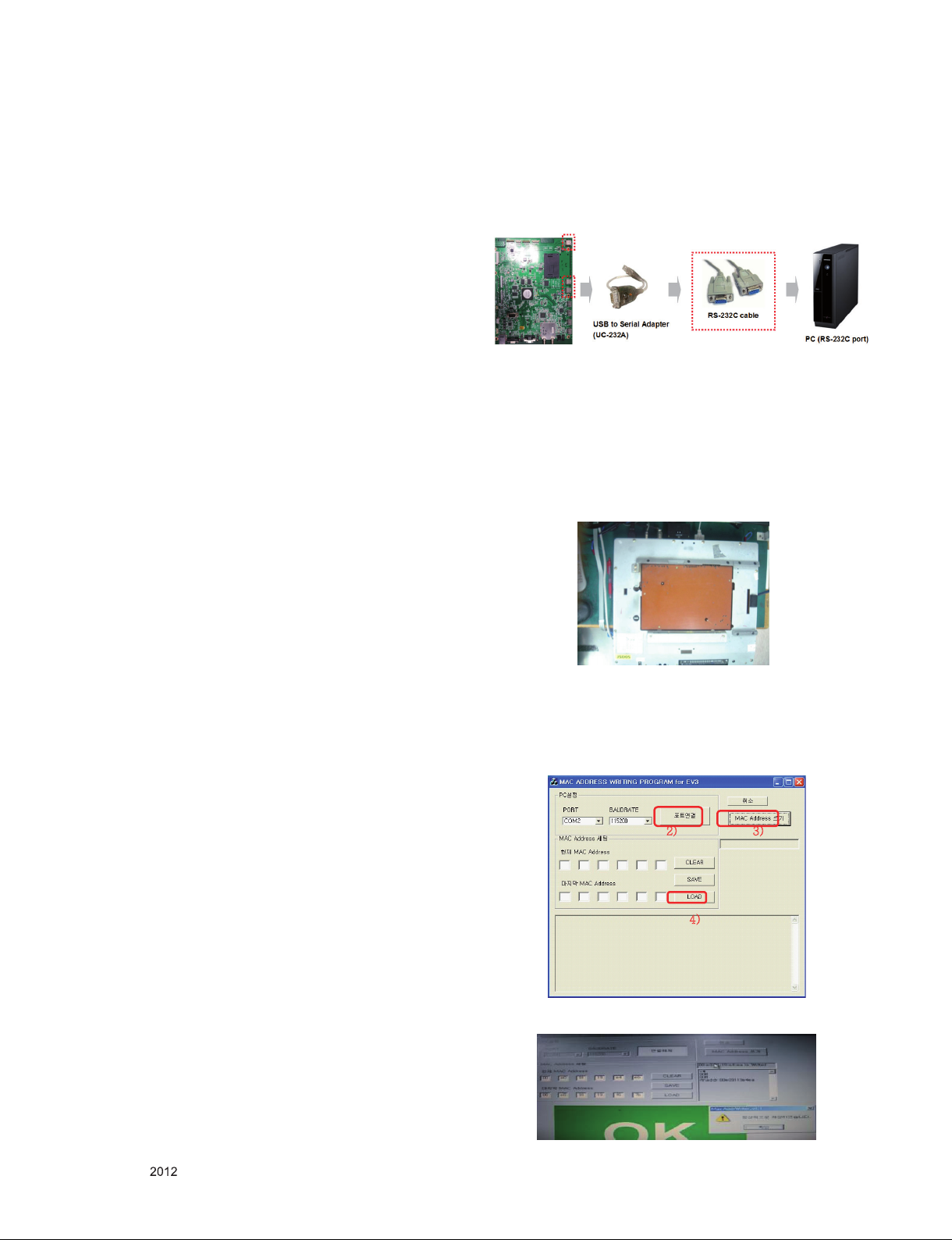
* RS-232Cの接続方法
接続:PCBA(USBポート)-> USB-シリアル アダプタ(UC-232A)>RS-232Cケーブル -> PC(RS-232Cポート)
▪ USB-シリアル アダプタの製品名はUC-232Aです。
☞ 注意 : LJ21*シャーシはUC-232Aドライバのみをサポートして
います。 (他のものは使用しないでください )
4. PCBアセンブリ調整方法
4.1. MACアドレスとMキーのダウンロード、LANテスト
4.1.1. MACアドレスのダウンロード
▪ プログラムのダウンロード:Serial.exe
4.1.1.1. 方法
(1) ジグをPCBAに接続します。
3. 調整項目
3.1. PCBアセンブリ調整項目
(1) Macアドレスのダウンロード、LANテスト
(2) メイン ソフトウェア プログラムのダウンロード:USBメモリ ス
ティックを使用
(3) 入力ツール - オプション
(4) EDIDのダウンロード:ツール オプションの調整時に、EDIDデ
ータは自動的にダウンロードされます。
(5) ADCキャリブレーション - RGBおよびコンポーネント
(6) ソフトウェア バージョンの確認
3.2. SETアセンブリ調整項目
(1) 地域オプションの入力
(2) ホワイト バランスの調整:自動
(3) ホワイト バランスの調整:手動
(4) インテリジェント センサー検査ガイド
(5) 局所輝度制御検査ガイド
(6) プリセット チャンネル情報
(7) 内部プリセット テスト
(8) モーション リモート コントローラ検査
(9) 3D機能テスト
(10) 出力条件の調整
(11) 音響仕様
(12) ファクタリング オプション データ入力
(2) PCで“Serial.exe”を実行し、MACアドレスを編集します(MAC
アドレスの開始と終了の入力)
(3) Comポートを接続します(ポート接続ボタンをクリック)
(4) MACアドレスを書き込むには、読み込みボタン(3)をクリック
します
(5) MACアドレスを書き込みます
(6) OKまたはNGを確認します。
Only for training and service purposes
- 9 -
LGE Internal Use OnlyCopyright © LG Electronics. Inc. All rights reserved.
Page 10
4.1.2. Mキーのダウンロード
MACアドレスの入力後、ジグおよびMキー ダウンロード プログ
ラムを使用して、Mキーのダウンロードを開始します。
4.1.3. Widevineキーのダウンロード
Mキーの入力後、ジグおよびWidevineキー ダウンロード プログ
ラムを使用して、Widevineキーのダウンロードを開始します。
4.1.4. ESNキーのダウンロード
Widevineキーの入力後、ジグおよびESNキー ダウンロード プロ
グラムを使用して、ESNキーのダウンロードを開始します。
4.1.5. DTCPキーのダウンロード
ESNキーの入力後、ジグおよびDTCPキー ダウンロード プログラ
ムを使用して、DTCPキーのダウンロードを開始します。
4.1.6. PINGテスト(LAN動作テスト)
4.1.6.1. PCBAの確認
(1) LANをPCBAに接続し、電源をオンにします。
(2) 調整用リモコンのADJ(調整)キーを押します。
(3) 「13. ACAP PING TEST」と入力し、ネットワークを確認します。
4.1.6.2. セットの確認
(1) クロスLANケーブルを使用してTVセットとPCを接続します。
(PC IP:12.12.2.3)
(2) “PINTテスト プログラム”を実行し、プログラムの設定データ
を確認します (TVセットのIP:12.12.2.2)。
(3) 調整用リモコンのPower Only(電源のみ)キーを押します。
(4) 実行をクリックし、[OK]または[NG]を確認します。
4.1.7. WIFI MACアドレスの確認
4.1.7.1. RS232コマンドによる方法
コマンド セットACK
Transmission
4.1.7.2. In-Startでのメニューの確認
[A][l][][Set ID][][20][Cr] [O][K][x] または [N][G]
4.2. メイン ソフトウェア プログラムのダウンロード
4.2.1. メモリ スティックの使用
▪ USBダウンロード:サービス モード
(1) USBメモリ スティックをUSBポートに差し込みます。
(2) ソフトウェア バージョンが自動的に検出されます。
-> ソフトウェアのダウンロード処理が自動的に実行されます。
(3) メモリからファイルをコピーしていることを示すメッセージが
表示されます。
Only for training and service purposes
- 10 -
(4) ダウンロードが完了すると、DCオフからDCオンに切り替わり
ます。
(5) TVをオンにして、更新されたソフトウェア バージョンとツール
オプションを確認します。
LGE Internal Use OnlyCopyright © LG Electronics. Inc. All rights reserved.
Page 11
4.3. 入力ツール オプション
▪ 調整ツール オプションについては、部品表を参照してください。
(1) ツール オプションの入力:PCBA確認プロセス
(2) 地域オプションの入力:アセンブリ プロセスの設定
*** ツール オプションの表
ツー
ツー
ツー
ツー
ツー
ツー
ル オ
ル オ
ル オ
ル オ
モデル
22LS3500
26LS3500
32LS3500
32LM5800
42LM5800
47LM5800
32LM6600
42LM6600
47LM6600
42LM7600
47LM7600
55LM7600
47LM9600
55LM9600
32LM6690
42LM6690
プショ
プショ
ン2
プショ
ン3
ン1
2337 8269 9053 14606 4189 279 4411
291 8269 9053 14606 4189 279 4411
292 8269 9053 14606 4189 1303 4411
100 8268 29533 14606 22621 1305 5947
102 8268 29533 14604 22621 1305 5947
103 8268 29533 14604 22621 1305 5947
164 41035 29533 14607 22679 1321 6075
166 41035 29533 14605 22679 1321 6075
167 41035 29533 14605 22679 1321 6075
198 41035 29533 14605 22679 1321 13627
199 41035 29533 14605 22679 1321 13627
201 41035 29533 14605 22679 1321 13627
32999 45131 29533 22799 22551 1321 14011
33001 45131 29533 22799 22551 1321 14011
164 41035 29533 14607 23199 1321 6075
166 41035 29533 14605 23199 1321 6075
プショ
ン4
ル オ
プショ
ン5
ツール オプションの入力およびACオフ後
PCBAチェックの前に、ツール オプションを変更し、ACをオフにしてか
らオンにする(プラグの抜き差し)を行う必要があります。
(この処理を怠ると、設定が異常になる可能性があります)
4.3.1. プロファイル:モジュールのメーカー、サイズ、および
市場に応じて一部の設定値が異なるため、 オプショ
ン値を変更する必要があります。
4.3.2. 装置:調整用リモコン
4.3.3. 調整方法
この入 力方法は他のシャーシと同じです(調整用リモコンの
ADJ(調整)キーを使用)。
(オプションを変更しない場合、入力メニューでモデル仕様が異
なる可能性があります)
オプション値については、各メイン シャーシ アッシーのジョブ表
現(EBTxxxxxxxx)を参照してください。
注:機能検査完了後に“IN-STOP(イン-停止)”キーを押さないで
ください。
ル オ
プショ
ン6
ツー
ル オ
プショ
ン7
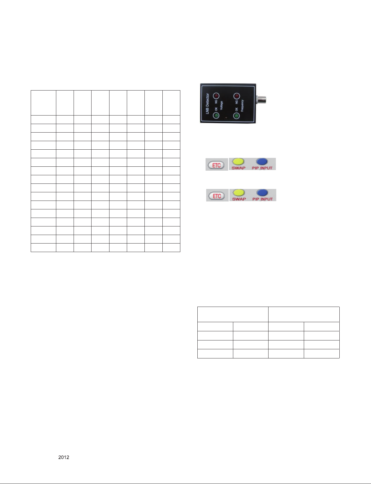
4.3.4. 衛星LNB 16V出力検査方法
4.3.4.1. 衛星LNB 16V出力検査 – 手動による確認
▪ 必要な装置
- 調整用リモコン
- LNB検出器
4.3.4.1.1. プロセス
(1) LNB検出器を接続します(衛星チューナー ジャック)。
(2) Power ONLY(電源のみ)キーを押します。
(3) その後、ETCとSWAPキーを同時に押します(LNB ON)。
(4) 数秒後、LNB検出器の緑のランプ(OK)が点灯します。
(5) ETCとPIP INPUT(PIP入力)キーを押します(LNB OFF)。
(6) オフにします(LNB検出器のすべてのライトがオフになりま
す)。
4.3.4.2. 衛星LNB 16V出力検査 - RS-232Cを使用
▪ 必要な装置
- 調整用リモコン
- LNB検出器
- RS – 232C
4.3.4.2.1. プロセス
(1) RS-232CケーブルとLNB検出器を接続します(衛星チューナー
ジャック)
(2) コマンド: AI 00 30 [DFT Command](自動的に完了):LNB
ON
AI 00 40 [DFT Command]:LNB OFF
LNB ON
AI 00 30(DFTコマンド)
18V LED ON 18V LED OFF
22KHZ LED OFF 22KHZ LED OFF
13V LED OFF 13V LED OFF
周波数LED OFF 周波数LED OFF
LNB OFF
AI 00 40(DFTコマンド)
Only for training and service purposes
- 11 -
LGE Internal Use OnlyCopyright © LG Electronics. Inc. All rights reserved.
Page 12
4.4. EDIDのダウンロード方法
EDIDをダウンロード中は、HDMIおよびRGB(D-SUB)ケーブルを接
続しないことを推奨します。 これが不可能な場合は、MSPG装置を接
続することを推奨します。
EDIDデータをダウンロードするには、次の2つの方法があります。
4.4.1. 第1の方法
EDIDデータは、ツール オプションの調整時に自動的にダウンロ
ードされます。
ツール オプション5を調整した後、Enterキーを押すと自動的にダ
ウンロードされます。
これには、約2秒かかります。
4.4.2. 第2の方法
注:ツール オプションが正しいかどうかを確認する必要がありま
す。
ツール オプションが不適切な場合、hdmi edidデータが正しくダ
ウンロードされないことがあります。
(1) ADJ(調整)キーを押します。
(2) [10. EDIDダウンロード]に移動し、正しい方向キー(▶)を押し
ます。
(3) 開始時に正しい方向キー(▶)を押します。
(4) 数秒後、待機のメッセージ => [OK]が表示され、完了します。
4.4.3. RS-232Cコマンドによる方法
コマンド:AE 00 10
=> 注 : EDIDをダウンロード中は、HDMIおよびRGB(D-SUB)ケ
ーブルを接続しないでください。
ケーブルを接続すると、EDIDのダウンロードが失敗しま
す。
4.4.3. EDIDデータ
4.4.3.1. HDモデル:LS3500(HDMI:3EA)
** Analog(RGB): 128bytes
0 1 2 3 4 5 6 7 8 9 A B C D E F
0 00 FF FF FF FF FF FF 00 1E 6D 01 00 01 01 01 01
10 01 16 01 03 68 A0 5A 78 0A EE 91 A3 54 4C 99 26
20 0F 50 54 A1 08 00 31 40 45 40 61 40 71 40 81 80
30 01 01 01 01 01 01 02 3A 80 18 71 38 2D 40 58 2C
40 45 00 A0 5A 00 00 00 1E 66 21 50 B0 51 00 1B 30
50 40 70 36 00 A0 5A 00 00 00 1E 00 00 00 FD 00 3A
60 3E 1E 53 10 00 0A 20 20 20 20 20 20 00 00 00 FC
70 00 4C 47 20 54 56 0A 20 20 20 20 20 20 20 00 5C
** HDMI 1 : 256Bytes
0 1 2 3 4 5 6 7 8 9 A B C D E F
0 00 FF FF FF FF FF FF 00 1E 6D 01 00 01 01 01 01
10 01 16 01 03 80 A0 5A 78 0A EE 91 A3 54 4C 99 26
20 0F 50 54 A1 08 00 31 40 45 40 61 40 71 40 81 80
30 01 01 01 01 01 01 02 3A 80 18 71 38 2D 40 58 2C
40 45 00 A0 5A 00 00 00 1E 66 21 50 B0 51 00 1B 30
50 40 70 36 00 A0 5A 00 00 00 1E 00 00 00 FD 00 3A
60 3E 1E 53 10 00 0A 20 20 20 20 20 20 00 00 00 FC
70 00 4C 47 20 54 56 0A 20 20 20 20 20 20 20 01 43
80 02 03 34 F1 48 90 22 20 05 04 03 02 01 29 35 17
90 48 15 07 50 09 57 07 78 03 0C 00 10 00 B8 2D 20
A0 C0 0E 01 4F 00 FE 08 10 06 10 18 10 28 10 38 10
B0 E3 05 03 01 02 3A 80 18 71 38 2D 40 58 2C 45 00
C0 A0 5A 00 00 00 1E 01 1D 80 18 71 1C 16 20 58 2C
D0 25 00 A0 5A 00 00 00 9E 01 1D 00 72 51 D0 1E 20
E0 6E 28 55 00 A0 5A 00 00 00 1E 26 36 80 A0 70 38
F0 1F 40 30 20 25 00 A0 5A 00 00 00 1A 00 00 00 20
** HDMI 2 : 256Bytes
0 1 2 3 4 5 6 7 8 9 A B C D E F
0 00 FF FF FF FF FF FF 00 1E 6D 01 00 01 01 01 01
10 01 16 01 03 80 A0 5A 78 0A EE 91 A3 54 4C 99 26
20 0F 50 54 A1 08 00 31 40 45 40 61 40 71 40 81 80
30 01 01 01 01 01 01 02 3A 80 18 71 38 2D 40 58 2C
40 45 00 A0 5A 00 00 00 1E 66 21 50 B0 51 00 1B 30
50 40 70 36 00 A0 5A 00 00 00 1E 00 00 00 FD 00 3A
60 3E 1E 53 10 00 0A 20 20 20 20 20 20 00 00 00 FC
70 00 4C 47 20 54 56 0A 20 20 20 20 20 20 20 01 43
80 02 03 34 F1 48 90 22 20 05 04 03 02 01 29 35 17
90 48 15 07 50 09 57 07 78 03 0C 00 20 00 B8 2D 20
A0 C0 0E 01 4F 00 FE 08 10 06 10 18 10 28 10 38 10
B0 E3 05 03 01 02 3A 80 18 71 38 2D 40 58 2C 45 00
C0 A0 5A 00 00 00 1E 01 1D 80 18 71 1C 16 20 58 2C
D0 25 00 A0 5A 00 00 00 9E 01 1D 00 72 51 D0 1E 20
E0 6E 28 55 00 A0 5A 00 00 00 1E 26 36 80 A0 70 38
F0 1F 40 30 20 25 00 A0 5A 00 00 00 1A 00 00 00 10
** HDMI 3 : 256Bytes
0 1 2 3 4 5 6 7 8 9 A B C D E F
0 00 FF FF FF FF FF FF 00 1E 6D 01 00 01 01 01 01
10 01 16 01 03 80 A0 5A 78 0A EE 91 A3 54 4C 99 26
20 0F 50 54 A1 08 00 31 40 45 40 61 40 71 40 81 80
30 01 01 01 01 01 01 02 3A 80 18 71 38 2D 40 58 2C
40 45 00 A0 5A 00 00 00 1E 66 21 50 B0 51 00 1B 30
50 40 70 36 00 A0 5A 00 00 00 1E 00 00 00 FD 00 3A
60 3E 1E 53 10 00 0A 20 20 20 20 20 20 00 00 00 FC
70 00 4C 47 20 54 56 0A 20 20 20 20 20 20 20 01 43
80 02 03 34 F1 48 90 22 20 05 04 03 02 01 29 35 17
90 48 15 07 50 09 57 07 78 03 0C 00 30 00 B8 2D 20
A0 C0 0E 01 4F 00 FE 08 10 06 10 18 10 28 10 38 10
B0 E3 05 03 01 02 3A 80 18 71 38 2D 40 58 2C 45 00
C0 A0 5A 00 00 00 1E 01 1D 80 18 71 1C 16 20 58 2C
D0 25 00 A0 5A 00 00 00 9E 01 1D 00 72 51 D0 1E 20
E0 6E 28 55 00 A0 5A 00 00 00 1E 26 36 80 A0 70 38
F0 1F 40 30 20 25 00 A0 5A 00 00 00 1A 00 00 00 00
Only for training and service purposes
- 12 -
LGE Internal Use OnlyCopyright © LG Electronics. Inc. All rights reserved.
Page 13
** HDMI 4 : 256Bytes
0 1 2 3 4 5 6 7 8 9 A B C D E F
0 00 FF FF FF FF FF FF 00 1E 6D 01 00 01 01 01 01
10 01 16 01 03 80 A0 5A 78 0A EE 91 A3 54 4C 99 26
20 0F 50 54 A1 08 00 31 40 45 40 61 40 71 40 81 80
30 01 01 01 01 01 01 02 3A 80 18 71 38 2D 40 58 2C
40 45 00 A0 5A 00 00 00 1E 66 21 50 B0 51 00 1B 30
50 40 70 36 00 A0 5A 00 00 00 1E 00 00 00 FD 00 3A
60 3E 1E 53 10 00 0A 20 20 20 20 20 20 00 00 00 FC
70 00 4C 47 20 54 56 0A 20 20 20 20 20 20 20 01 43
80 02 03 34 F1 48 90 22 20 05 04 03 02 01 29 35 17
90 48 15 07 50 09 57 07 78 03 0C 00 40 00 B8 2D 20
A0 C0 0E 01 4F 00 FE 08 10 06 10 18 10 28 10 38 10
B0 E3 05 03 01 02 3A 80 18 71 38 2D 40 58 2C 45 00
C0 A0 5A 00 00 00 1E 01 1D 80 18 71 1C 16 20 58 2C
D0 25 00 A0 5A 00 00 00 9E 01 1D 00 72 51 D0 1E 20
E0 6E 28 55 00 A0 5A 00 00 00 1E 26 36 80 A0 70 38
F0 1F 40 30 20 25 00 A0 5A 00 00 00 1A 00 00 00 F0
(太字) チェックサム: トータルのEDIDデータにより変わる可能性があ
ります。
EDID C/Sデータ 10ビットFHD
HDMI RGB
EDID C/Sデータ ブロック0 0x43 0x5C
ブロック1 0x20(HDMI1)
0x10(HDMI2)
0x00(HDMI3)
0XF0(HDMI4)
4.4.3.2. 3D M0DEL(濃色のサポートなし):42 / 4 7 / 55LM7600
(HDMI:4EA)
** Analog(RGB): 128bytes
0 1 2 3 4 5 6 7 8 9 A B C D E F
0 00 FF FF FF FF FF FF 00 1E 6D 01 00 01 01 01 01
10 01 16 01 03 68 A0 5A 78 0A EE 91 A3 54 4C 99 26
20 0F 50 54 A1 08 00 31 40 45 40 61 40 71 40 81 80
30 01 01 01 01 01 01 02 3A 80 18 71 38 2D 40 58 2C
40 45 00 A0 5A 00 00 00 1E 66 21 50 B0 51 00 1B 30
50 40 70 36 00 A0 5A 00 00 00 1E 00 00 00 FD 00 3A
60 3E 1E 53 10 00 0A 20 20 20 20 20 20 00 00 00 FC
70 00 4C 47 20 54 56 0A 20 20 20 20 20 20 20 00 5C
** HDMI 1 : 256Bytes
0 1 2 3 4 5 6 7 8 9 A B C D E F
0 00 FF FF FF FF FF FF 00 1E 6D 01 00 01 01 01 01
10 01 16 01 03 80 A0 5A 78 0A EE 91 A3 54 4C 99 26
20 0F 50 54 A1 08 00 31 40 45 40 61 40 71 40 81 80
30 01 01 01 01 01 01 02 3A 80 18 71 38 2D 40 58 2C
40 45 00 A0 5A 00 00 00 1E 66 21 50 B0 51 00 1B 30
50 40 70 36 00 A0 5A 00 00 00 1E 00 00 00 FD 00 3A
60 3E 1E 53 10 00 0A 20 20 20 20 20 20 00 00 00 FC
70 00 4C 47 20 54 56 0A 20 20 20 20 20 20 20 01 43
80 02 03 34 F1 48 90 22 20 05 04 03 02 01 29 35 17
90 48 15 07 50 09 57 07 78 03 0C 00 10 00 80 2D 20
A0 C0 0E 01 4F 00 FE 08 10 06 10 18 10 28 10 38 10
B0 E3 05 03 01 02 3A 80 18 71 38 2D 40 58 2C 45 00
C0 A0 5A 00 00 00 1E 01 1D 80 18 71 1C 16 20 58 2C
D0 25 00 A0 5A 00 00 00 9E 01 1D 00 72 51 D0 1E 20
E0 6E 28 55 00 A0 5A 00 00 00 1E 26 36 80 A0 70 38
F0 1F 40 30 20 25 00 A0 5A 00 00 00 1A 00 00 00 58
** HDMI 2 : 256Bytes
0 1 2 3 4 5 6 7 8 9 A B C D E F
0 00 FF FF FF FF FF FF 00 1E 6D 01 00 01 01 01 01
10 01 16 01 03 80 A0 5A 78 0A EE 91 A3 54 4C 99 26
20 0F 50 54 A1 08 00 31 40 45 40 61 40 71 40 81 80
30 01 01 01 01 01 01 02 3A 80 18 71 38 2D 40 58 2C
40 45 00 A0 5A 00 00 00 1E 66 21 50 B0 51 00 1B 30
50 40 70 36 00 A0 5A 00 00 00 1E 00 00 00 FD 00 3A
60 3E 1E 53 10 00 0A 20 20 20 20 20 20 00 00 00 FC
70 00 4C 47 20 54 56 0A 20 20 20 20 20 20 20 01 43
80 02 03 34 F1 48 90 22 20 05 04 03 02 01 29 35 17
90 48 15 07 50 09 57 07 78 03 0C 00 20 00 80 2D 20
A0 C0 0E 01 4F 00 FE 08 10 06 10 18 10 28 10 38 10
B0 E3 05 03 01 02 3A 80 18 71 38 2D 40 58 2C 45 00
C0 A0 5A 00 00 00 1E 01 1D 80 18 71 1C 16 20 58 2C
D0 25 00 A0 5A 00 00 00 9E 01 1D 00 72 51 D0 1E 20
E0 6E 28 55 00 A0 5A 00 00 00 1E 26 36 80 A0 70 38
F0 1F 40 30 20 25 00 A0 5A 00 00 00 1A 00 00 00 48
Only for training and service purposes
- 13 -
LGE Internal Use OnlyCopyright © LG Electronics. Inc. All rights reserved.
Page 14
** HDMI 3 : 256Bytes
0 1 2 3 4 5 6 7 8 9 A B C D E F
0 00 FF FF FF FF FF FF 00 1E 6D 01 00 01 01 01 01
10 01 16 01 03 80 A0 5A 78 0A EE 91 A3 54 4C 99 26
20 0F 50 54 A1 08 00 31 40 45 40 61 40 71 40 81 80
30 01 01 01 01 01 01 02 3A 80 18 71 38 2D 40 58 2C
40 45 00 A0 5A 00 00 00 1E 66 21 50 B0 51 00 1B 30
50 40 70 36 00 A0 5A 00 00 00 1E 00 00 00 FD 00 3A
60 3E 1E 53 10 00 0A 20 20 20 20 20 20 00 00 00 FC
70 00 4C 47 20 54 56 0A 20 20 20 20 20 20 20 01 43
80 02 03 34 F1 48 90 22 20 05 04 03 02 01 29 35 17
90 48 15 07 50 09 57 07 78 03 0C 00 30 00 80 2D 20
A0 C0 0E 01 4F 00 FE 08 10 06 10 18 10 28 10 38 10
B0 E3 05 03 01 02 3A 80 18 71 38 2D 40 58 2C 45 00
C0 A0 5A 00 00 00 1E 01 1D 80 18 71 1C 16 20 58 2C
D0 25 00 A0 5A 00 00 00 9E 01 1D 00 72 51 D0 1E 20
E0 6E 28 55 00 A0 5A 00 00 00 1E 26 36 80 A0 70 38
F0 1F 40 30 20 25 00 A0 5A 00 00 00 1A 00 00 00 38
** HDMI 4 : 256Bytes
0 1 2 3 4 5 6 7 8 9 A B C D E F
0 00 FF FF FF FF FF FF 00 1E 6D 01 00 01 01 01 01
10 01 16 01 03 80 A0 5A 78 0A EE 91 A3 54 4C 99 26
20 0F 50 54 A1 08 00 31 40 45 40 61 40 71 40 81 80
30 01 01 01 01 01 01 02 3A 80 18 71 38 2D 40 58 2C
40 45 00 A0 5A 00 00 00 1E 66 21 50 B0 51 00 1B 30
50 40 70 36 00 A0 5A 00 00 00 1E 00 00 00 FD 00 3A
60 3E 1E 53 10 00 0A 20 20 20 20 20 20 00 00 00 FC
70 00 4C 47 20 54 56 0A 20 20 20 20 20 20 20 01 43
80 02 03 34 F1 48 90 22 20 05 04 03 02 01 29 35 17
90 48 15 07 50 09 57 07 78 03 0C 00 40 00 80 2D 20
A0 C0 0E 01 4F 00 FE 08 10 06 10 18 10 28 10 38 10
B0 E3 05 03 01 02 3A 80 18 71 38 2D 40 58 2C 45 00
C0 A0 5A 00 00 00 1E 01 1D 80 18 71 1C 16 20 58 2C
D0 25 00 A0 5A 00 00 00 9E 01 1D 00 72 51 D0 1E 20
E0 6E 28 55 00 A0 5A 00 00 00 1E 26 36 80 A0 70 38
F0 1F 40 30 20 25 00 A0 5A 00 00 00 1A 00 00 00 28
(太字) チェックサム: トータルのEDIDデータにより変わる可能性があ
ります。
EDID C/Sデータ 8ビットFHD
HDMI RGB
EDID C/Sデータ ブロック0 0x43 0x5C
ブロック1 0x58(HDMI1)
0x48(HDMI2)
0x38(HDMI3)
0X28(HDMI4)
4.4.3.3. 3D M0DEL(濃色のサポートなし):32 / 4 2 / 47LM6600
(HDMI:4EA)、32/42/47LM5800(HDMI:3EA)
** Analog(RGB): 128bytes
0 1 2 3 4 5 6 7 8 9 A B C D E F
0 00 FF FF FF FF FF FF 00 1E 6D 01 00 01 01 01 01
10 01 16 01 03 68 A0 5A 78 0A EE 91 A3 54 4C 99 26
20 0F 50 54 A1 08 00 31 40 45 40 61 40 71 40 81 80
30 01 01 01 01 01 01 02 3A 80 18 71 38 2D 40 58 2C
40 45 00 A0 5A 00 00 00 1E 66 21 50 B0 51 00 1B 30
50 40 70 36 00 A0 5A 00 00 00 1E 00 00 00 FD 00 3A
60 3E 1E 53 10 00 0A 20 20 20 20 20 20 00 00 00 FC
70 00 4C 47 20 54 56 0A 20 20 20 20 20 20 20 00 5C
** HDMI 1 : 256Bytes
0 1 2 3 4 5 6 7 8 9 A B C D E F
0 00 FF FF FF FF FF FF 00 1E 6D 01 00 01 01 01 01
10 01 16 01 03 80 A0 5A 78 0A EE 91 A3 54 4C 99 26
20 0F 50 54 A1 08 00 31 40 45 40 61 40 71 40 81 80
30 01 01 01 01 01 01 02 3A 80 18 71 38 2D 40 58 2C
40 45 00 A0 5A 00 00 00 1E 66 21 50 B0 51 00 1B 30
50 40 70 36 00 A0 5A 00 00 00 1E 00 00 00 FD 00 3A
60 3E 1E 53 10 00 0A 20 20 20 20 20 20 00 00 00 FC
70 00 4C 47 20 54 56 0A 20 20 20 20 20 20 20 01 43
80 02 03 34 F1 48 90 22 20 05 04 03 02 01 29 35 17
90 48 15 07 50 09 57 07 78 03 0C 00 10 00 80 2D 20
A0 C0 0E 01 4F 00 FE 08 10 06 10 18 10 28 10 38 10
B0 E3 05 00 00 02 3A 80 18 71 38 2D 40 58 2C 45 00
C0 A0 5A 00 00 00 1E 01 1D 80 18 71 1C 16 20 58 2C
D0 25 00 A0 5A 00 00 00 9E 01 1D 00 72 51 D0 1E 20
E0 6E 28 55 00 A0 5A 00 00 00 1E 26 36 80 A0 70 38
F0 1F 40 30 20 25 00 A0 5A 00 00 00 1A 00 00 00 5C
** HDMI 2 : 256Bytes
0 1 2 3 4 5 6 7 8 9 A B C D E F
0 00 FF FF FF FF FF FF 00 1E 6D 01 00 01 01 01 01
10 01 16 01 03 80 A0 5A 78 0A EE 91 A3 54 4C 99 26
20 0F 50 54 A1 08 00 31 40 45 40 61 40 71 40 81 80
30 01 01 01 01 01 01 02 3A 80 18 71 38 2D 40 58 2C
40 45 00 A0 5A 00 00 00 1E 66 21 50 B0 51 00 1B 30
50 40 70 36 00 A0 5A 00 00 00 1E 00 00 00 FD 00 3A
60 3E 1E 53 10 00 0A 20 20 20 20 20 20 00 00 00 FC
70 00 4C 47 20 54 56 0A 20 20 20 20 20 20 20 01 43
80 02 03 34 F1 48 90 22 20 05 04 03 02 01 29 35 17
90 48 15 07 50 09 57 07 78 03 0C 00 20 00 80 2D 20
A0 C0 0E 01 4F 00 FE 08 10 06 10 18 10 28 10 38 10
B0 E3 05 00 00 02 3A 80 18 71 38 2D 40 58 2C 45 00
C0 A0 5A 00 00 00 1E 01 1D 80 18 71 1C 16 20 58 2C
Only for training and service purposes
- 14 -
LGE Internal Use OnlyCopyright © LG Electronics. Inc. All rights reserved.
Page 15
D0 25 00 A0 5A 00 00 00 9E 01 1D 00 72 51 D0 1E 20
E0 6E 28 55 00 A0 5A 00 00 00 1E 26 36 80 A0 70 38
F0 1F 40 30 20 25 00 A0 5A 00 00 00 1A 00 00 00 4C
** HDMI 3 : 256Bytes
0 1 2 3 4 5 6 7 8 9 A B C D E F
0 00 FF FF FF FF FF FF 00 1E 6D 01 00 01 01 01 01
10 01 16 01 03 80 A0 5A 78 0A EE 91 A3 54 4C 99 26
20 0F 50 54 A1 08 00 31 40 45 40 61 40 71 40 81 80
30 01 01 01 01 01 01 02 3A 80 18 71 38 2D 40 58 2C
40 45 00 A0 5A 00 00 00 1E 66 21 50 B0 51 00 1B 30
50 40 70 36 00 A0 5A 00 00 00 1E 00 00 00 FD 00 3A
60 3E 1E 53 10 00 0A 20 20 20 20 20 20 00 00 00 FC
70 00 4C 47 20 54 56 0A 20 20 20 20 20 20 20 01 43
80 02 03 34 F1 48 90 22 20 05 04 03 02 01 29 35 17
90 48 15 07 50 09 57 07 78 03 0C 00 30 00 80 2D 20
A0 C0 0E 01 4F 00 FE 08 10 06 10 18 10 28 10 38 10
B0 E3 05 00 00 02 3A 80 18 71 38 2D 40 58 2C 45 00
C0 A0 5A 00 00 00 1E 01 1D 80 18 71 1C 16 20 58 2C
D0 25 00 A0 5A 00 00 00 9E 01 1D 00 72 51 D0 1E 20
E0 6E 28 55 00 A0 5A 00 00 00 1E 26 36 80 A0 70 38
F0 1F 40 30 20 25 00 A0 5A 00 00 00 1A 00 00 00 3C
** HDMI 3 : 256Bytes
0 1 2 3 4 5 6 7 8 9 A B C D E F
0 00 FF FF FF FF FF FF 00 1E 6D 01 00 01 01 01 01
10 01 16 01 03 80 A0 5A 78 0A EE 91 A3 54 4C 99 26
20 0F 50 54 A1 08 00 31 40 45 40 61 40 71 40 81 80
30 01 01 01 01 01 01 02 3A 80 18 71 38 2D 40 58 2C
40 45 00 A0 5A 00 00 00 1E 66 21 50 B0 51 00 1B 30
50 40 70 36 00 A0 5A 00 00 00 1E 00 00 00 FD 00 3A
60 3E 1E 53 10 00 0A 20 20 20 20 20 20 00 00 00 FC
70 00 4C 47 20 54 56 0A 20 20 20 20 20 20 20 01 43
80 02 03 34 F1 48 90 22 20 05 04 03 02 01 29 35 17
90 48 15 07 50 09 57 07 78 03 0C 00 40 00 80 2D 20
A0 C0 0E 01 4F 00 FE 08 10 06 10 18 10 28 10 38 10
B0 E3 05 00 00 02 3A 80 18 71 38 2D 40 58 2C 45 00
C0 A0 5A 00 00 00 1E 01 1D 80 18 71 1C 16 20 58 2C
D0 25 00 A0 5A 00 00 00 9E 01 1D 00 72 51 D0 1E 20
E0 6E 28 55 00 A0 5A 00 00 00 1E 26 36 80 A0 70 38
F0 1F 40 30 20 25 00 A0 5A 00 00 00 1A 00 00 00 2C
(太字) チェックサム: トータルのEDIDデータにより変わる可能性があ
ります。
EDID C/Sデータ 8ビットFHD
HDMI RGB
EDID C/Sデータ ブロック0 0x43 0x5C
ブロック1 0x5C(HDMI1)
0x4C(HDMI2)
0x3C(HDMI3)
0x2C(HDMI4)
4.5. ソフトウェア バージョンの確認
4.5.1. 方法
(1) 調整用リモコンのIn-start(イン-開始)キーを押します。
(2) ソフトウェア バージョン チェック(例: 47LM7600-JA)
IN START 調整チェック
モデル名 :GLOBAL-
シリアル番号 : SKJY1107 3.電源オフステ
S/W Version(ソ
フトウェア バージ
ョン)
MICOMバージョン :Vx.xx.x 5.システム2 国 - -
BOOTバージョン :xx.xx.xx 6.システム3 2. ツール オプション
FRCバージョン :x.xx 7.モデル番号ダウン
PWM(最小/最
大/3Dデューテ
ィー)
EDID(RGB/HDMI) :x.xx / x.xx 9.スペクトラム拡散 ツール オプション4 6412
チップタイプ :MTK5369 10.同期レベル ツール オプション5 6731
Wi-Fiバージョン :x.x 11.ステーブル カ
Wi-Fiチャンネル :x 12.SDPサーバー選択 ツール オプション7 63
Wi-Fi MAC :
MACアドレス :
IPアドレス :x:x:x:x 15.RFリモコン テスト コンポーネント OK
Widevine :OK RGB OK
RFレシーバ バー
ジョン
PLAT4
:00.00.xx. xx 4.システム1 国グループ JP
:10 / 100 / 100 8.テスト オプション ツール オプション3 4959
FF:FF:FF:FF:FF:FF
FF:FF:FF:FF:FF:FF
:xx.xx.xx 5. EDID OK
1.調整チェック
▶
2.ADCデータ 1. 国グループ([OK]を押して
ータス
ロード
ウント
13.ネットワーク エラ
ー履歴
14.アンテナ 4. ADC調整 OK
保存)
国グループ コード 18
ツール オプション1 34805
ツール オプション2 32779
ツール オプション6 89
3. ホワイト バラン
ス調整
OK
Only for training and service purposes
- 15 -
LGE Internal Use OnlyCopyright © LG Electronics. Inc. All rights reserved.
Page 16
A. Demod F/Wバ
ージョン
A. Demod F/Wバ
ージョン
デバッグ ステ
ータス
アクセスUSBステ
ータス
UTT:XXX HDMI4 OK
APP履歴バージョン :x.x
アイQゲイン:xxxx
PQL DB:LGD_X
:Null RGB OK
(0X97)
:Null RGB OK
(0X7E 、
0XC9)
:DEBUG HDMI2 OK
(0X7E 、
0XC9)
0/0(T) /0(C) HDMI3 OK
(0X7E 、
0XB9)
(0X7E 、
0XA9)
5. SETアセンブリ調整方法
5.1. 地域オプションの入力
(1) プロファイル:各国の言語および信号条件が異なるため、地域
オプションを変更する 必要があります。
(2) 装置:調整用リモコン
(3) 調整方法
- この入力方法は他のシャーシと同じです(調整用リモコンの
IN-START(イン-開始)キーを使用)。
オプション値については、各メイン シャーシ アッシーのジョブ表
現(EBTxxxxxxxx)を参照してください
5.2. ホワイト バランスの調整:(自動調整の場合)
▪
目的: モジュールの色温度の偏差を少なくするために、色温度
を調整します。
▪
基本: サチュレーションなしてホワイト バランスを調整するに
はR/G/Bゲインのいずれかを192(デフォルトのデータ)
に固定し、その他を減らします。
▪
調整モード: – 高/中/低
※必要な装置
- 調整用リモコン
- カラー アナライザ:CA100+、CA-210、また同等の製品(CS-1000
でキャリブレーションされたチャンネルで使用する必要がありま
す)。
- LCD TV:CH-9
- PDP TV:CH-10
- ホワイトLED TV:CH-14
- RGB LED(MNT):CH-16
- 自動ホワイト バランス調整装置(自動調整用)
5.2.1. ホワイト バランスの調整:(自動調整の場合)
▪ 測定用装置の接続図(自動調整用)
Color Analyzer
Probe
RS-232C
※
Signal Source
※If TV internal pattern is used, not needed
Pattern Generator
RS-232C
Computer
RS-232C
(1) POWER ON(電源オン)キーを使用してTVを調整モードに設
定します。
(2) ゼロ キャリブレーション プローブをディスプレイの中心に配
置します。
(3) ケーブル(RS-232C)を接続します。
(4) 調整プログラムのモードを選択し、 調整を開始します。
(5) 調整が 完了(OKの表示)したら、モードの調整ステータス、
低、中、高を確認します。
(6) プローブとRS-232Cケーブルを取り外して、調整を終了します。
▪ ホワイト バランス調整は、 コマンド“wb 00 00”で開始し、コマ
ンド“wb 00 ff ”で終了する必要があります。必要に応じて オフ
セットを調整します
5.3. ホワイト バランスの調整(手動調整の場合)
▪
CS-1000でキャリブレーションされたチャンネルでカラー アナ
ライザ(CA100+、CA210)を使用する必要があります。
▪
CA100+またはCA-210のゼロ キャリブレーションを実行して、
調整時にセンサーをモジュールに貼り付けます。
▪
手動調整の場合、以下のシーケンスで調整することもできま
す。
(1) 調整用リモコンのPOWER ON(電源オン)キーを押して、ヒート
ランのホワイト パターンを選択します。次に、ヒート ランを15
分以上実行します。
( この手順を実行しない場合、ホワイト バランスの条件が変わ
る可能性があります)。
(2) Exit(終了)キーを押します。
(3) リモコンでAVモードに変更します。
(4) 外部パターン(80%ホワイト パターン)を入力します。
(5) ADJ(調整)キーを押します。=>“0000”と入力します(パスワー
ド)。
(6) 次に、[3. ホワイト バランス調整]を選択します。
(7) ホワイト バランス調整モードに入ります。
(8) センサーを画面の中央に貼り付けて、各項目(Red/Green/Blue
ゲインおよびオフセット)を選択します(リモコンの▲/▼(CH
+/-)キーを使用)。
(9) R/G/Bゲインを調整します(◀/▶(VOL +/-)キーを使用)。
(10) 3つのモード(高/中/低)すべてを調整します。R/G/Bゲインの
いずれかを修正してその他を変更します。
(11) 調整が完了したら、“COPY ALL”と入力します。
(12) リモコンのEXIT(終了)キーを押して調整モードを終了しま
す。
Only for training and service purposes
- 16 -
LGE Internal Use OnlyCopyright © LG Electronics. Inc. All rights reserved.
Page 17
※ 例
最初に目標値(x, y)から離れた座標を調整します。
(1) x, y 〉目標値
ⅰ) R、Gを減らします。
(2) x, y〈 目標値
ⅰ) まずBゲインを減らします。
ⅱ) 他のいずれかを減らします。
(3) x 〉目標値、y〈 目標値
ⅰ) まずBを減らして、yを目標値よりも少し大きくします。
ⅱ) Rを減らしてx値を調整します。
(4) x 〈 目標値、y 〉目標値
ⅰ) まずBを減らして、xを目標値よりも少し大きくします。
ⅱ) Gを減らしてx値を調整します。
▪
CA100+またはCA210装置を使用する場合の標準色座標と温
度
モード
高 0.271±0.002 0.270±0.002 13000K -0.003
中 0.286±0.002 0.289±0.002 9,300K -0.003
低 0.314±0.002 0.318±0.002 6,500K -0.003
色座標
X Y
温度 △uv 備考
変更理由:ビビッド モードの場合は、他の会社のセットよりも詳細
なため。
- LV、LW、LZシリーズ (LGD LEDモジュールの場合、エイジングに
よって色座標が変化しています。このため、下の表を使用する必
要があります)。
SETエイジング時間による色座標のタイム テーブル(LGDモジュ
ールのみ。ただし、CMIモジュールは除く)
(1) モデル: 26/32LS3500、32/42/47LM5800、32/42/47LM6600、
42LM7600, 32/42LM6690 (Normal line)
ステ
ージ
エイジング
時間
(最小)
1 0-2 282 284 297 303 321 326
2 3-5 281 282 296 301 320 324
3 6-9 279 281 294 300 318 323
4 10-19 278 280 293 299 317 322
5 20-35 276 277 291 296 315 319
6 36-49 274 274 289 293 313 316
7 50-79 273 272 288 291 312 314
8 80-119 272 271 287 290 311 313
9 Over 120 271 270 286 289 310 312
高 中 低
X Y X Y X Y
271 270 286 289 314 318
(2) モデル: 26/32LS3500, 32/42/47LM5800, 32/42/47LM6600,
42LM7600, 32/42LM6690 (aging Chamber)
ステ
ージ
エイジング
時間
(最小)
1 0-2 278 279 293 298 317 321
2 3-5 276 277 291 296 315 319
3 6-9 275 275 290 294 314 317
4 10-19 274 273 289 292 313 315
5 20-35 273 271 288 290 312 313
6 36-49 272 269 287 288 311 311
7 50-79 268 266 283 285 307 308
8 80-119 266 264 281 283 305 306
9 Over 120 265 263 280 282 304 305
高 中 低
X Y X Y X Y
271 270 286 289 314 318
■ SET応用LGD LEDモジュールでは、LEDモジュールの物理的特性の
ために、
SETのエイジングを190分実行して色座標を安定化させます。
このため、ホワイト バランス制御装置は、SETからSETエイジング時
間を取得する必要があり、 そのたびに改訂された色座標によりホ
ワイト バランスを制御する必要があります。
- ホワイト バランス座標をチェックするには、下記の条件で測定す
る必要があります。
映像モード:標準を選択し、次のように変更します。
ダイナミック コントラスト:オフ、
ダイナミック カラー:オフ、
クリア ホワイト:オフ
=> 映像モードの変更:標準 => 標準(ユーザー)
(上記の条件が失われた場合、ホワイト バランスの
座標が仕様未満になることがあります)。
Only for training and service purposes
- 17 -
LGE Internal Use OnlyCopyright © LG Electronics. Inc. All rights reserved.
Page 18
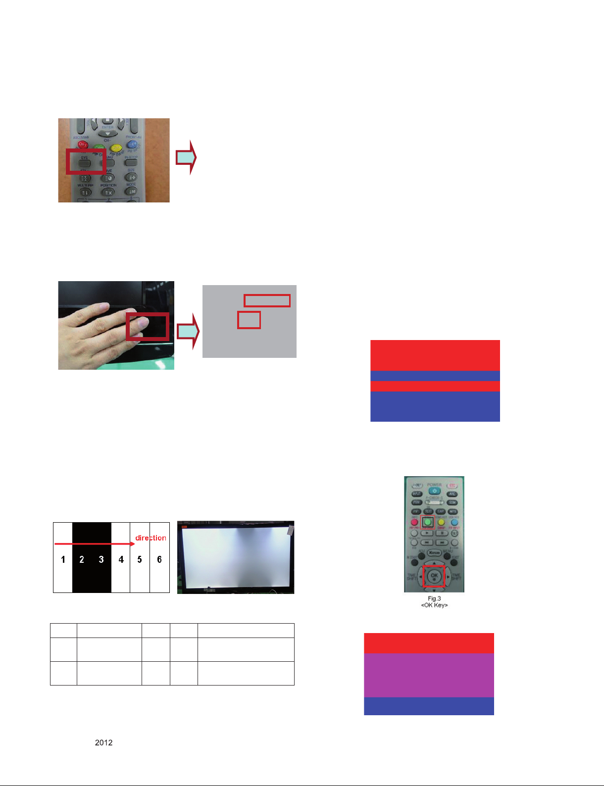
5.4. インテリジェント センター検査ガイド
ステップ1. TVセットをオンにします。
ステップ2. 調整用リモコンの“EYE”ボタンを押します。
ステップ3. 前面C/Aのインテリジェント センサー モジュールを約
6秒間手で覆います。
センサー データが20未満の場合は、“OK”メッセージが表示され
ます。
=> “OK”メッセージが表示されない場合は、センサー モジュール
が故障しています。
良品と交換する必要があります。
Green Eye-Check
Sensor Data : 492
BackLight : 100
OK
5.7. モーション リモート コントローラ検査
5.7.1. 装置
テスト用モーション リモート コントローラ、テスト用IR-KEY-CODE
リモート コントローラ
テスト前にバッテリを確認します。 (推奨:ロットごとにバッテリを
変更します)。
5.7.1. プロセス
(1) TVセットとモーション リモコンのペアリングのために、“Mute(
ミュート)”または“ START(開始)”キーを押します。
(2) “OK”または“Enter”キーを押すと、画面にカーソルが表示され
ます。
(3) “Vol+(ボリューム+)”または“STOP(停止)”キーを押して、ペア
リングを解消します。
5.8. 3D機能テスト
5.8.1. 装置
パターン ジェネレータMSHG-600、MSPG-6100、HDMIモード872
、パターン番号 83
5.8.2. プロセス
(1) 下のように3Dテスト パターンを入力します(HDMIモデル番号
872、パターン番号83)
ステップ4. “OK”メッセージの表示を確認したら、センサー モジュ
ールから手を離します。
=> センサー データの値が“0”から“300”に変わるかどうかを確認
します。
値が変化しない場合は、センサーが故障しています。
交換する必要があります。
5.5. 局所輝度制御検査ガイド(オプション)
5.5.1. 局所輝度制御機能付きエッジLEDモデル
(1) 調整用リモコンの"TILT(チルト)"キーを押して、 移動パターン
を確認します。 ブラック バー パターンが左から右に動きます。
局所輝度制御機能が機能しない場合、画面全体にフル ホワイ
ト が表示されます。
5.6. 高電位(Hi-pot)テスト
番号 項目 値 単位 備考
1. 耐電圧(AC<>FG)
2. 耐電圧(FGなし) 3
1.5
kV 100 mA、1秒(ライン)
1.5
3
100 mA、1分(OQC)
kV 100 mA、1秒(ライン)
100 mA、1分(OQC)
O
K
Fig.1
<HDMI Mode 872, Pattern No. 83>
(2) 3D OSDが自動表示されたら、緑色のボタンを選択します。
(3) 3Dメガネをかけずに、下の図をチェックします。
O K
Only for training and service purposes
- 18 -
LGE Internal Use OnlyCopyright © LG Electronics. Inc. All rights reserved.
Page 19
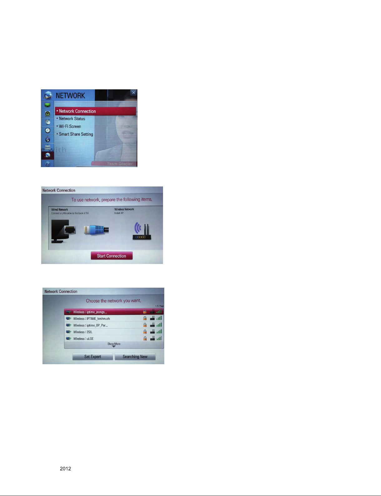
5.9. Wi-Fiテスト
5.9.1. プロセス
(1) TVをオンにします
(2) ネットワークメニューで、ネットワーク接続オプションを選択し
ます。
(3) ネットワーク接続で、接続開始ボタンを選択します。
(4) 下の図のように何らかのAPが検出された場合、システムは正
常に動作しています。
Only for training and service purposes
- 19 -
LGE Internal Use OnlyCopyright © LG Electronics. Inc. All rights reserved.
Page 20
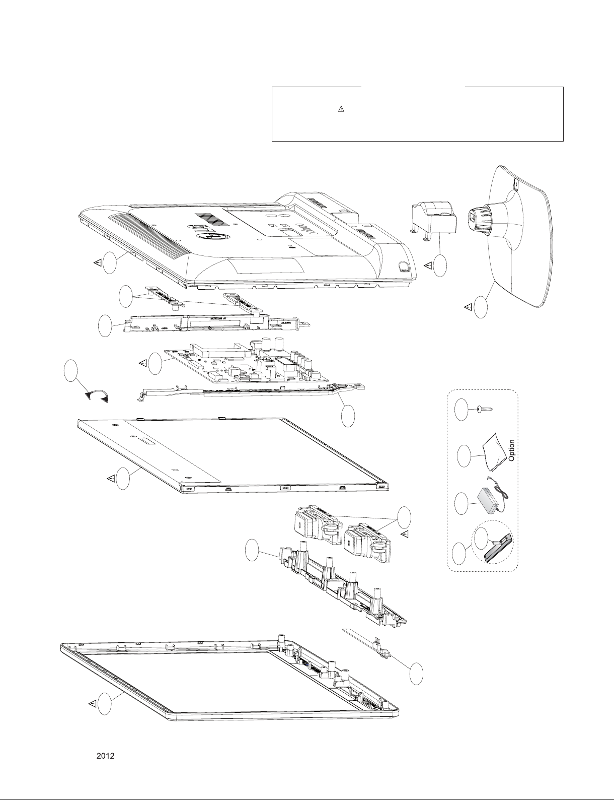
分 解 図
IMPORTANT SAFETY NOTICE
Many electrical and mechanical parts in this chassis have special safety-related characteristics. These
parts are identified by in the Schematic Diagram and EXPLODED VIEW.
It is essentia l t hat these special safety parts sho uld be replaced with the same comp onents as
recommended in this manual to prevent X-RADIATION, Shock, Fire, or other Hazards.
Do not modify the original design without permission of manufacturer.
400
910
410
900
521
LV1
540
820
A10
* Set + Stand
A5
200
A31
120
A21
310
A2
300
Only for training and service purposes
- 20 -
510
LGE Internal Use OnlyCopyright © LG Electronics. Inc. All rights reserved.
Page 21
EAX6430790* : LD22* / LC22*
Copyright ⓒ 2012 LG Electronics. Inc. All right reserved.
Only for training and service purposes
LGE Internal Use Only
EAX6443420* : LT22* / LJ22* / LA22* / LB22*
Crystal Matching Test result
: 27pF -> 20pF -> 24pF
+3.3V_NORMAL
R103
4.7K
R104
4.7K
OPT
R105
4.7K
OPT
NVRAM
IC104
AT24C256C-SSHL-T
A0
1
A1
2
A2
3
GND
4
VCC
8
WP
7
SCL
6
SDA
5
NVRAM_ATMEL
HDCP EEPROM
HDCP_EEPROM_ST
IC100
M24C16-R
NC_1
NC_2
NC_3
VSS
VCC
8
1
WC
2
7
SCL
3
6
SDA
4
5
+3.3V_NORMAL
+3.3V_NORMAL
R181 4.7K
R191 22
R192 22
IC104-*1
M24256-BRMN6TP
E0
VCC
1
8
WC
E1
7
2
SCL
E2
6
3
SDA
VSS
5
4
NVRAM_ST
Write Protection
- Low : Normal Operation
- High : Write Protection
R136 33
R137 33
HDCP_EEPROM_MICRO
C101
0.1uF
16V
VSS
I2C_SCL1
I2C_SDA1
A0
A1
A2
I2C_SCL5
I2C_SDA5
IC100-*1
24LC16B
1
2
3
4
IC104-*2
R1EX24256BSAS0A
A0
1
A1
2
A2
3
VSS
4
NVRAM_RENESAS
VCC
8
WP
7
SCL
6
SDA
5
VCC
8
WP
7
SCL
6
SDA
5
JTAG
JTRST#
JTDI
JTMS
JTCLK
JTDO
R143 33
MTK_JTAG
AR100
+3.3V_NORMAL
R147
1K
OPT
R148
1K
I2C_1 : AMP, L/DIMMING,HDCP KEY
I2C_2 : T-CON
I2C_3 : MICOM
I2C_4 : S/Demod,T2/Demod, LNB
I2C_5 : NVRAM
I2C_6 : TUNER_MOPLL(T/C,ATV)
R160
R186
R156
2.7K
4.7K
2.7K
R189
4.7K
MTK_EPI
R164
2.7K
MTK_DVB_C2_TUNER
R177
2.7K
MODEL_OPT_0
MODEL_OPT_1
I2C_SCL1
I2C_SDA1
I2C_SCL2
I2C_SDA2
I2C_SCL3
I2C_SDA3
I2C_SCL4
I2C_SDA4
I2C_SCL5
I2C_SDA5
I2C_SCL6
I2C_SDA6
STB_SCL
STB_SDA
OPCTRL_11_SCL
OPCTRL_10_SDA
OSCL1
OSDA1
OSCL2
OSDA2
OSCL0
OSDA0
OPCTRL_1_SCL
OPCTRL_0_SDA
+3.3V_NORMAL
I2C
R110 33
R111 33
R112 33
R113 33
R114 33
R115 33
R116 33
R117 33
R118 33
R121 33
R122 33
R123 33
R106
R101
4.7K
MTK_FRC3/URSA5
MTK_Int_FRC/URSA5
R128
R131
1.2K
1.2K
Model Option
R125
4.7K
R108
4.7K
4.7K
MTK_FHD
MTK_OPTIC_Tx_IC
R134
R139
2.7K
2.7K
R130
4.7K
MTK_3D_DEPTH_IC
R142
2.7K
R132
4.7K
MTK_CP_BOX
MTK_DDR_768MB
R135
R173
2.7K
4.7K
+3.3V_NORMAL
R188
R185
2.7K
2.7K
R140
4.7K
R175
4.7K
MTK_DVB_S_TUNER
MTK_DVB_T2_TUNER
MODEL_OPT_2
MODEL_OPT_3
/S2_RESET
MODEL_OPT_4
MODEL_OPT_5
MODEL_OPT_6
R102
4.7K
R107
4.7K
MTK_NO_FRC/FRC3
MTK_NO_FRC/Int_FRC
R109
MTK_HD
4.7K
R129
4.7K
R127
4.7K
MTK_NON_OPTIC_Tx_IC
MTK_NON_3D_DEPTH_IC
R133
4.7K
R138
4.7K
MTK_NON_CP_BOX
MTK_DDR_DEFAULT
R141
4.7K
MTK_NON_DVB_T2_TUNER
R187
R184
4.7K
MTK_NON_DVB_S_TUNER
MTK_NON_DVB_C2_TUNER
4.7K
R190
4.7K
MTK_NON_EPI
M_RFModule_ISP
MODEL_OPT_8
MODEL_OPT_9
MODEL_OPT_10
MODEL_OPT_7
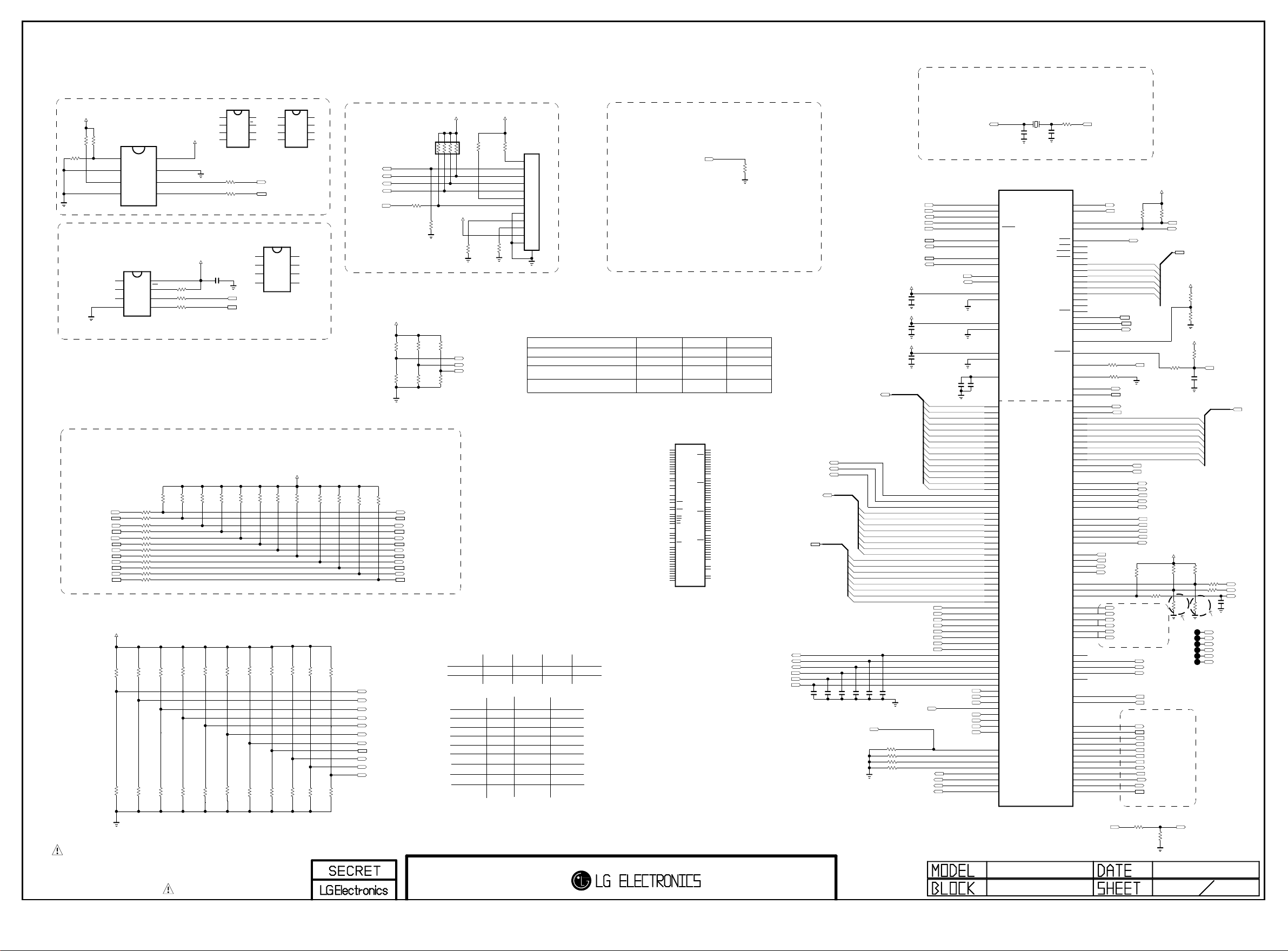
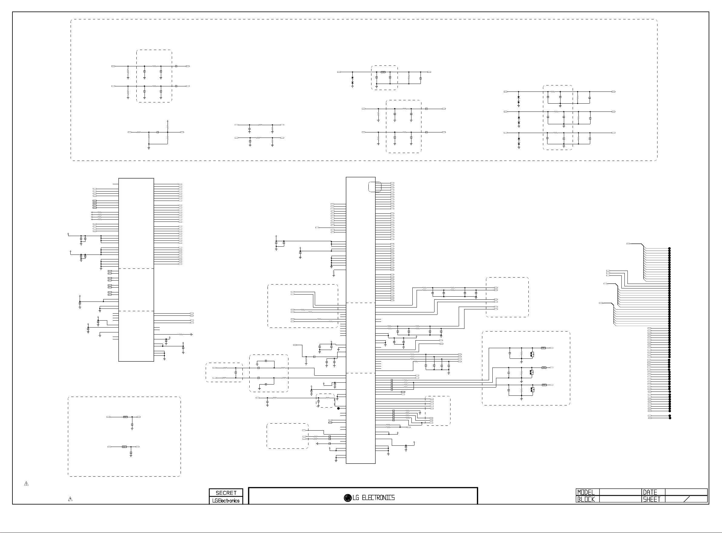
THE SYMBOL MARK OF THIS SCHEMETIC DIAGRAM INCORPORATES
SPECIAL FEATURES IMPORTANT FOR PROTECTION FROM X-RADIATION.
FILRE AND ELECTRICAL SHOCK HAZARDS, WHEN SERVICING IF IS
ESSENTIAL THAT ONLY MANUFATURES SPECFIED PARTS BE USED FOR
THE CRITICAL COMPONENTS IN THE SYMBOL MARK OF THE SCHEMETIC.
10K
R150
1K
R151
1K
OPT
+3.3V_NORMAL
+3.3V_NORMAL
R144
10K
MTK_JTAG
R153
1K
OPT
R154
1K
+3.3V_NORMAL
R146
10K
MTK_JTAG
R149
R145
10K
10K
MTK_JTAG
LED_PWM0
LED_PWM1
OPCTRL3
NO_FRC
MODEL_OPT_0
MODEL_OPT_1
0
0
MODEL_OPT_2
MODEL_OPT_3
MODEL_OPT_4
MODEL_OPT_5
MODEL_OPT_6
MODEL_OPT_7
MODEL_OPT_8
MODEL_OPT_9
MODEL_OPT_10
3D DEPTH
DDR
CP BOX
T2 Tuner
S Tuner
Reserved
EPI
MODEL OPTION 8 is just for CP Box
It should not be appiled at MP
MTK_JTAG
R152
1K
12507WS-12L
MTK_JTAG
P100
1
2
3
4
5
6
7
8
9
10
11
12
13
Close to eMMC Flash
(IC8100)
EMMC_CLK
STRAPPING LED_PWM0 LED_PWM1 OPCTRL3
ICE mode + 27M + Serial boot 0 0 0
ICE mode + 27M + ROM to Nand boot 0 0 1
ICE mode + 27M + Rom to eMMC boot 0 1 0
from eMMC pins (share pins w/s NAND)
ICE mode + 27M + ROM to eMMC boot 0 1 1
from SDIO pins
MT5369_RM
IC105-*1
LGE2112-AL
SoC
internal
FRC
0
1
HIGH
FHD
OPTIC
3D_Depth_IC
DDR_768MB
Enable
Support
Support
LG FRC2
1
0
LOW
HD
NON_OPTIC
NON_3D_Depth_IC
DDR_Default
Disable
Not Support
Not Support
Reserved
1
1
AC1
AC2
A3
A4
B4
C4
D4
B3
C3
AC3
AC4
G10
G9
G13
G21
F10
D9
C9
A20
A21
E18
F17
E17
E16
D14
B14
A13
G11
D16
F18
C15
A15
F13
C14
F11
E15
D13
B15
E14
F16
E13
B13
A14
F14
F15
C19
DDRV_44
ARDQM0
C21
DDRV_45
ARDQS0
B21
DDRV_1
ARDQS0
C23
ARDQ0
DDRV_2
B17
ARDQ1
DDRV_5
D23
ARDQ2
DDRV_8
C17
ARDQ3
DDRV_10
D24
ARDQ4
DDRV_4
C16
ARDQ5
DDRV_7
C24
ARDQ6
DDRV_46
D15
ARDQ7
DDRV_47
D21
ARDQM1
MEMTP
B20
ARDQS1
MEMTN
C20
ARDQS1
A17
ARDQ8
RVREF_B
A23
ARDQ9
RVREF_A
D17
ARDQ10
B23
ARDQ11
D20
ARDQ12
ARCKE
D22
ARDQ13
D19
ARDQ14
ARCLK1
C22
ARDQ15
ARCLK1
A7
ARCLK0
ARDQM2
B9
ARCLK0
ARDQS2
A9
ARDQS2
C12
ARODT
ARDQ16
D6
ARRAS
ARDQ17
B12
ARCAS
ARDQ18
C5
ARCS
ARDQ19
C13
ARWE
ARDQ20
A5
ARDQ21
A12
ARRESET
ARDQ22
B5
ARDQ23
ARBA0
E10
ARBA1
ARDQM3
C8
ARBA2
ARDQS3
D8
ARDQS3
C6
ARDQ24
ARCSX
D10
ARDQ25
D7
ARDQ26
ARA14
C11
ARDQ27
ARA13
C7
ARDQ28
ARA12
C10
ARDQ29
ARA11
B7
ARDQ30
ARA10
B10
ARDQ31
ARA9
ARA8
ARA7
N14
AVDD33_MEMPLL
ARA6
N15
AVSS33_MEMPLL
ARA5
ARA4
ARA3
R1
DVSS_50
ARA2
P21
DVSS_48
ARA1
ARA0
Default
Support
Not Support
R174
10K
MT5369_MIVAL_ERR
MT5369_MISTRT
SOC -> CI SLOT
MT5369_TS_OUT[0-7]
CI_DATA[0-7]
/USB_OCD2
/USB_OCD1
/USB_OCD3
USB_CTL2
USB_CTL1
USB_CTL3
SOC -> CI SLOT
MT5369_MCLKI
C100
0.1uF
OPT
C102
0.1uF
OPT
CI_ADDR[0-14]
CI SLOT -> SOC
C103
C105
0.1uF
0.1uF
OPT
OPT
SC_ID_SOC
CI_DATA[0]
CI_DATA[1]
CI_DATA[2]
CI_DATA[3]
CI_DATA[4]
CI_DATA[5]
CI_DATA[6]
CI_DATA[7]
C104
C106
0.1uF
0.1uF
OPT
R193
R176
R162
R163
MODEL_OPT_4
AVDD_33SB
AVDD_33SB
VDD3V3
MT5369_TS_OUT[0]
MT5369_TS_OUT[1]
MT5369_TS_OUT[2]
MT5369_TS_OUT[3]
MT5369_TS_OUT[4]
MT5369_TS_OUT[5]
MT5369_TS_OUT[6]
MT5369_TS_OUT[7]
MT5369_TS_IN[0]
MT5369_TS_IN[1]
MT5369_TS_IN[2]
MT5369_TS_IN[3]
MT5369_TS_IN[4]
MT5369_TS_IN[5]
MT5369_TS_IN[6]
MT5369_TS_IN[7]
ERROR_OUT
OPT
MODEL_OPT_7
NON_EU
10K
10K
10K
10K
M_RFModule_RESET
JTCLK
JTDI
JTDO
JTMS
JTRST#
OSDA0
OSCL0
OSDA1
OSCL1
MT5369_XTAL_OUT
C116
0.1uF
C117
0.1uF
C118
0.1uF
OPC_EN
/TU_RESET
/S2_RESET
MT5369_XTAL_IN
C107
2.2uF
10V
CI_ADDR[0]
CI_ADDR[1]
CI_ADDR[2]
CI_ADDR[3]
CI_ADDR[4]
CI_ADDR[5]
CI_ADDR[6]
CI_ADDR[7]
CI_ADDR[8]
CI_ADDR[9]
CI_ADDR[10]
CI_ADDR[11]
CI_ADDR[12]
CI_ADDR[13]
CI_ADDR[14]
EPI_LOCK6
MODEL_OPT_0
MODEL_OPT_1
MODEL_OPT_3
M_RFModule_ISP
MODEL_OPT_5
MODEL_OPT_6
X-TAL
C108
2.2uF
10V
AP14
AM14
AR14
AR15
AN14
AP12
AN12
AP15
AN15
AT34
AU34
AK27
AH26
AK18
AK17
AK23
AM27
AJ20
AN23
AN24
AP23
AR23
AU23
AT23
AM24
AM23
H32
F37
F36
G37
G36
G35
G34
H34
L34
L32
K33
K32
H33
L35
K36
J32
J34
K34
K35
K37
J36
J37
J35
J33
G33
H35
H31
F34
E36
N33
P32
M35
M37
M33
F35
E35
E37
N32
M34
M36
M32
L33
E33
E32
F32
A29
D31
C31
E30
E31
F31
E29
AP9
AT9
AR9
AU9
X100
27MHz
C113
24pF
MT5369_NON_RM
IC105
LGE2112
JTCK
JTDI
JTDO
JTMS
JTRST
OSDA0
OSCL0
OSDA1
OSCL1
XTALI
XTALO
AVDD33_XTAL_STB
AVSS33_XTAL_STB
AVDD33_VGA_STB
AVSS33_VGA_STB
AVDD33_PLLGP
AVSS33_PLLGP
AVDD10_LDO
GPIO0
GPIO1
GPIO2
GPIO3
GPIO4
GPIO5
GPIO6
GPIO7
GPIO8
GPIO9
GPIO10
GPIO11
GPIO12
GPIO13
GPIO14
GPIO15
GPIO16
GPIO17
GPIO18
GPIO19
GPIO20
GPIO21
GPIO22
GPIO23
GPIO24
GPIO25
GPIO26
GPIO27
GPIO28
GPIO29
GPIO30
GPIO31
GPIO32
GPIO33
GPIO34
GPIO35
GPIO36
GPIO37
GPIO38
GPIO39
GPIO40
GPIO41
GPIO42
GPIO43
GPIO44
GPIO45
GPIO46
GPIO47
GPIO48
GPIO49
GPIO50
GPIO51
GPIO52
GPIO53
GPIO54
GPIO55
ADIN0_SRV
ADIN1_SRV
ADIN2_SRV
ADIN3_SRV
ADIN4_SRV
ADIN5_SRV
ADIN6_SRV
ADIN7_SRV
MID_MAIN_1
C115
24pF
U0TX
U0RX
U1RX
U1TX
POWE
POOE
POCE1
POCE0
PDD7
PDD6
PDD5
PDD4
PDD3
PDD2
PDD1
PDD0
PARB
PACLE
PAALE
EMMC_CLK
OPWRSB
ORESET
OIRI
FSRC_WR
STB_SCL
STB_SDA
DEMOD_RST
DEMOD_TSCLK
DEMOD_TSDATA0
DEMOD_TSDATA1
DEMOD_TSDATA2
DEMOD_TSDATA3
DEMOD_TSDATA4
DEMOD_TSDATA5
DEMOD_TSDATA6
DEMOD_TSDATA7
DEMOD_TSSYNC
DEMOD_TSVAL
CI_INT
CI_TSCLK
CI_TSDATA0
CI_TSSYNC
CI_TSVAL
PVR_TSCLK
PVR_TSVAL
PVR_TSSYNC
PVR_TSDATA0
PVR_TSDATA1
SPI_CLK1
SPI_CLK
SPI_DATA
SPI_CLE
OPWM2
OPWM1
OPWM0
SD_D0
SD_D1
SD_D2
SD_D3
SD_CMD
SD_CLK
LDM_CS
LDM_CLK
LDM_VSYNC
LDM_DO
LDM_DI
LED_PWM1
LED_PWM0
OPCTRL11
OPCTRL10
OPCTRL9
OPCTRL8
OPCTRL7
OPCTRL6
OPCTRL5
OPCTRL4
OPCTRL3
OPCTRL2
OPCTRL1
OPCTRL0
IC
R119
MT5369_XTAL_OUTMT5369_XTAL_IN
0
+3.3V_NORMAL
AR18
AP18
AU16
AT16
A35
C33
B34
D33
D29
C30
D30
B31
A31
B32
A32
C32
D32
A34
C34
C29
AM20
SOC_TX
SOC_RX
EMMC_DATA[7]
EMMC_DATA[6]
EMMC_DATA[5]
EMMC_DATA[4]
EMMC_DATA[3]
EMMC_DATA[2]
EMMC_DATA[1]
R165
4.7K
EMMC_CMD
EMMC_DATA[0]
EMMC_CLK
R167
4.7K
M_REMOTE_RX
M_REMOTE_TX
+3.3V_NORMAL
+3.3V_NORMAL
EMMC_DATA[2-7]
AM22
AU21
D27
AT21
AR21
T34
T32
T36
U36
T33
T30
V33
V32
V31
V30
T35
T31
N36
T37
R35
R37
R36
R34
R32
R33
P33
P34
N37
P35
N34
N35
AU12
AT12
AR12
A37
C35
A36
B35
B36
B37
AT11
AU11
AR10
AM9
AP10
AN22
AP21
AU20
AT20
AN18
AP20
AM18
AN19
AP19
AR19
AN21
AM19
AN20
AR20
AMP_RESET_SOC AMP_RESET_N
OPT
R159 4.7K
STB_SCL
STB_SDA
PCM_RST
FE_TS_CLK
/CI_CD2
/CI_CD1
/PCM_IORD
/PCM_IOWR
SMARTCARD_CLK
SMARTCARD_PWR_SEL
SMARTCARD_RST
SMARTCARD_DET
SMARTCARD_VCC
SMARTCARD_DATA
AMP_RESET_BY_SOC
FOR JAPAN
R124
33
IR
FE_TS_DATA[0]
FE_TS_DATA[1]
FE_TS_DATA[2]
FE_TS_DATA[3]
FE_TS_DATA[4]
FE_TS_DATA[5]
FE_TS_DATA[6]
FE_TS_DATA[7]
FE_TS_SYNC
FE_TS_VAL
/PCM_REG
/PCM_CE1
MT5369_TS_SYNC
/PCM_WE
/PCM_OE
MT5369_TS_VAL
CI_A_VS1
MT5369_TS_CLK
/PCM_IRQA
/PCM_WAIT
+3.3V_NORMAL
R166
2.7K
OPT
R169 10K
OPT
L/DIM0_SCLK
L/DIM0_VS
L/DIM0_MOSI
LED_PWM1
LED_PWM0
5V Tolerance
OPCTRL_11_SCL
OPCTRL_10_SDA
COMP1_DET
SC_DET
DSUB_DET
HP_DET
AV1_CVBS_DET
AMP_RESET_SOC
OPCTRL3
RF_SWITCH_CTL
OPCTRL_1_SCL
OPCTRL_0_SDA
R100
10K
R172
22
CI SLOT -> SOC
CI SLOT -> SOC
CI SLOT -> SOC
R168
4.7K
OPT
R120
1K
PWM1_PULL_DOWN_1K
AMP_RESET_BY_SOC
33
R158
2011.12.13
8
R157
4.7K
OPT
R178
4.7K
OPT
R155
10K
OPT
SOC_RESET
C114
0.1uF
16V
FE_TS_DATA[0-7]
EXTERNAL DEMOD
-> SOC
R161
4.7K
OPT
R171
22
22
R170
R126
1K
PWM2_PULL_DOWN_1K
SMARTCARD_CLK
SMARTCARD_PWR_SEL
SMARTCARD_RST
SMARTCARD_DET
SMARTCARD_VCC
SMARTCARD_DATA
FOR JAPAN
C120
2.2uF
10V
OPT
PWM_DIM2
PWM_DIM1
A_DIM
Page 22
PLACE AT JACK SIDE
Copyright ⓒ 2012 LG Electronics. Inc. All right reserved.
Only for training and service purposes
LGE Internal Use Only
DDC_SCL_2_JACK
DDC_SCL_3_JACK
DDC_SCL_1_SOC
DDC_SCL_4_JACK
DDC_SDA_2_JACK
DDC_SDA_3_JACK
DDC_SDA_1_SOC
DDC_SDA_4_JACK
5V_HDMI_2_JACK
5V_HDMI_3_JACK
5V_HDMI_1_SOC
5V_HDMI_4_JACK
HDMI_HPD_2_JACK
HDMI_HPD_3_JACK
HDMI_HPD_1_SOC
HDMI_HPD_4_JACK
+1.2V_MTK_AVDD
C303
0.1uF
VDD3V3
C304
0.1uF
Port was changed !!!!
VDD3V3
C308
0.1uF
C302
0.1uF
VDD3V3
C306
0.1uF
0.1uF
C307
R304
R305
R306
R307 1K
USB_DP3
USB_DM3
USB_DP2
USB_DM2
WIFI_DP
USB_DP1
USB_DM1
+1.2V_MTK_AVDD
C316
0.1uF
HP_LOUT_AMP
HP_ROUT_AMP
1K
1K
1K
WIFI_DM
PC_L_IN
PC_R_IN
AA32
AG33
AE33
AC33
AH32
AF33
AD33
AB33
AH33
AG31
AE31
AC31
AH31
AG32
AE32
AC32
AJ32
AA24
Y24
W24
AB24
AB29
AA29
Y29
AC29
AB30
AD30
AF31
AF32
C36
C37
D36
D37
AT13
AU13
AT14
AU14
D35
AP13
D34
AR13
W35
W34
Y34
Y35
U24
V24
W30
W36
W37
BLM18PG121SN1D
BLM18PG121SN1D
R300
470K
OPT
R301
470K
OPT
HDMI_CEC
HDMI_0_SCL
HDMI_1_SCL
HDMI_2_SCL
HDMI_3_SCL
HDMI_0_SDA
HDMI_1_SDA
HDMI_2_SDA
HDMI_3_SDA
HDMI_0_PWR5V
HDMI_1_PWR5V
HDMI_2_PWR5V
HDMI_3_PWR5V
HDMI_0_HPD
HDMI_1_HPD
HDMI_2_HPD
HDMI_3_HPD
AVDD12_HDMI_0_RX
AVDD12_HDMI_1_RX
AVDD12_HDMI_2_RX
AVDD12_HDMI_3_RX
AVDD33_HDMI_0_RX
AVDD33_HDMI_1_RX
AVDD33_HDMI_2_RX
AVDD33_HDMI_3_RX
AVSS33_HDMI_RX_1
AVSS33_HDMI_RX_2
AVSS33_HDMI_RX_3
AVSS33_HDMI_RX_4
USB_DP_P0
USB_DM_P0
USB_DP_P1
USB_DM_P1
USB_DP_P2
USB_DM_P2
USB_DP_P3
USB_DM_P3
AVDD33_USB_P0P1
AVDD33_USB_P2P3
AVSS33_USB_P1
AVSS33_USB_P2
PCIE11_TXP
PCIE11_TXN
PCIE11_RXN
PCIE11_RXP
AVDD12_PCIE11
AVDD33_PCIE11
AVSS12_PCIE11
PCIE11_REFCKN
PCIE11_REFCKP
HP_OUT
L303
HP_OUT
L302
Place at JACK SIDE
ARC
IC105
LGE2112
HP_OUT
C332
0.22uF
10V
HP_OUT
C331
0.22uF
10V
R302
180
HDMI_0_RX_0B
HDMI_0_RX_1B
HDMI_0_RX_2B
HDMI_0_RX_CB
HDMI_1_RX_0B
HDMI_1_RX_1B
HDMI_1_RX_2B
HDMI_1_RX_CB
HDMI_2_RX_0B
HDMI_2_RX_1B
HDMI_2_RX_2B
HDMI_2_RX_CB
HDMI_3_RX_0B
HDMI_3_RX_1B
HDMI_3_RX_2B
HDMI_3_RX_CB
HP_ROUT
1608 sizs For EMI
C300
560pF
50V
OPT
1608 sizs For EMI
C301
560pF
50V
OPT
R303
82
HDMI_0_RX_0
HDMI_0_RX_1
HDMI_0_RX_2
HDMI_0_RX_C
HDMI_1_RX_0
HDMI_1_RX_1
HDMI_1_RX_2
HDMI_1_RX_C
HDMI_2_RX_0
HDMI_2_RX_1
HDMI_2_RX_2
HDMI_2_RX_C
HDMI_3_RX_0
HDMI_3_RX_1
HDMI_3_RX_2
HDMI_3_RX_C
TXVP_0
TXVN_0
RXVN_1
RXVP_1
PHYLED1
PHYLED0
REXT
AVDD12_REC
AVDD33_COM
AVDD33_LD
AVSS33_LD
AVSS33_COM
AVSS12_REC
HP_LOUT
R314
0
R336
0
10V
C311 1uF
AG35
AG34
AG37
AG36
AF35
AF34
AH35
AH34
AE37
AE36
AD35
AD34
AC35
AC34
AE35
AE34
AB35
AB34
AA35
AA34
AA37
AA36
AC37
AC36
AK35
AK34
AJ35
AJ34
AJ37
AJ36
AJ33
AK33
AT18
AU18
AU17
AT17
AN16
AM16
AD15
AD14
AD16
AD17
AL16
AL15
AL14
C314
100pF
50V
OPT
C315
100pF
50V
OPT
+5V_NORMAL
R308
1.2K
OPT
R309
100K
+1.2V_MTK_AVDD
C323
0.1uF
C319
10uF
16V
C320
10uF
16V
D0+_HDMI2_JACK
D0-_HDMI2_JACK
D1+_HDMI2_JACK
D1-_HDMI2_JACK
D2+_HDMI2_JACK
D2-_HDMI2_JACK
CK+_HDMI2_JACK
CK-_HDMI2_JACK
D0+_HDMI3_JACK
D0-_HDMI3_JACK
D1+_HDMI3_JACK
D1-_HDMI3_JACK
D2+_HDMI3_JACK
D2-_HDMI3_JACK
CK+_HDMI3_JACK
CK-_HDMI3_JACK
D0+_HDMI1_SOC
D0-_HDMI1_SOC
D1+_HDMI1_SOC
D1-_HDMI1_SOC
D2+_HDMI1_SOC
D2-_HDMI1_SOC
CK+_HDMI1_SOC
CK-_HDMI1_SOC
D0+_HDMI4_JACK
D0-_HDMI4_JACK
D1+_HDMI4_JACK
D1-_HDMI4_JACK
D2+_HDMI4_JACK
D2-_HDMI4_JACK
CK+_HDMI4_JACK
CK-_HDMI4_JACK
R31524K
VDD3V3
C328
0.1uF
HDMI_ARC
PC_L_IN_SOC
PC_R_IN_SOC
EPHY_TDP
EPHY_TDN
EPHY_RDN
EPHY_RDP
IF_P
Close to Tuner
IF_N
DSUB_VSYNC
DSUB_HSYNC
T/C&AT&CHB
R346 0
R331 0
T/C&AT&CHB
1608 sizs For EMI
AOCLKN
AOCLKP
AECLKN
AECLKP
BOCLKN
BOCLKP
BECLKN
BECLKP
AR0_ADAC
AL0_ADAC
AR1_ADAC
AL1_ADAC
AR2_ADAC
AL2_ADAC
AR3_ADAC
AL3_ADAC
AVDD33_DAC
AVSS33_DAC
ASPDIF0
ASPDIF1
AOBCK
AOLRCK
AOMCLK
AOSDATA4
AOSDATA3
AOSDATA2
AOSDATA1
AOSDATA0
HSYNC
VSYNC
VGA_SDA
VGA_SCL
VDACX_OUT
VDACY_OUT
AVDD12_RGB
AVSS12_RGB
AO3N
AO3P
AO4N
AO4P
AO2N
AO2P
AO1N
AO1P
AO0N
AO0P
AE4N
AE4P
AE3N
AE3P
AE2N
AE2P
AE1N
AE1P
AE0N
AE0P
BO4N
BO4P
BO3N
BO3P
BO2N
BO2P
BO1N
BO1P
BO0N
BO0P
BE4N
BE4P
BE3N
BE3P
BE2N
BE2P
BE1N
BE1P
BE0N
BE0P
ALIN
COM
SOG
COM1
PB1P
PR1P
Y1P
SOY1
COM0
PB0P
PR0P
Y0P
SOY0
R328
470K
OPT
R329
470K
OPT
AG3
AG4
AG1
AG2
AF3
AF4
AE3
AE4
AE1
AE2
AD1
AD2
AL3
AL4
AL1
AL2
AK3
AK4
AJ3
AJ4
AJ1
AJ2
AH3
AH4
AT2
AU2
AT1
AU1
AR1
AR2
AP1
AP2
AN1
AN2
AM3
AM4
AT6
AU6
AP6
AR6
AP5
AR5
AT4
AU4
AP4
AR4
AP3
AR3
AN35
AN34
AM32
AM34
AM37
AM33
AM36
AM35
AG30
AF30
AK30
AE30
Y33
AR16
Y32
AR11
AP11
AM12
AM10
AM11
AN11
AN10
AN9
AN25
AM25
AR25
RP
AR24
GP
AU24
BP
AP24
AT24
AR22
AP22
AT26
AR26
AP26
AU26
AP25
AU28
AT28
AR28
AP27
AR27
AU30
AP29
AD20
AD21
AD19
AJ22
AJ21
AL24
R333
120-ohm
C344
27pF
50V
OPT
CHANGE SYMBOL
OPT
C348
100pF
50V
1608 sizs For EMI
C338
560pF
50V
OPT
1608 sizs For EMI
C339
560pF
50V
OPT
TXC4N
TXC4P
TXC3N
TXC3P
TXCCLKN
TXCCLKP
TXC2N
TXC2P
TXC1N
TXC1P
TXC0N
TXC0P
TXD4N
TXD4P
TXD3N
TXD3P
TXDCLKN
TXDCLKP
TXD2N
TXD2P
TXD1N
TXD1P
TXD0N
TXD0P
TXA4N
TXA4P
TXA3N
TXA3P
TXACLKN
TXACLKP
TXA2N
TXA2P
TXA1N
TXA1P
TXA0N
TXA0P
TXB4N
TXB4P
TXB3N
TXB3P
TXBCLKN
TXBCLKP
TXB2N
TXB2P
TXB1N
TXB1P
TXB0N
TXB0P
R3761.2K
R3771.2K
C397
1200pF
C365
0.01uF
Don’t use as GPIO
C3660.01uF
C3670.01uF
C3680.01uF
C3690.01uF
C3701500pF
C3710.01uF
C3720.01uF
C3730.01uF
C3740.01uF
C3751500pF
R3490
R3500
VDD3V3
R344
30K
R345
30K
CH3
CH1
CH6
CH5
CH4
CH2
C380
0.1uF
R366 100
R367 100
R368 100
RGB_DDC_SDA
RGB_DDC_SCL
R330
75
1%
C342
100pF
50V
C343
100pF
50V
C398
1200pF
R371 100
R356100
R357100
R358100
R359100
R361100
R362100
R363100
R364100
DTV/MNT_V_OUT_SOC
+1.2V_MTK_AVDD
C382
0.1uF
C340
47pF
50V
C345
10uF
16V
C346
10uF
16V
HP_OUT
HP_OUT
R3781.2K
R3791.2K
DAC_3V3
DSUB_HSYNC_SOC
DSUB_VSYNC_SOC
R3511.2K
R3521.2K
C399
1200pF
C387
22pF
OPT
For PCB Pattern
COMP1_Pb_SOC
COMP1_Pr_SOC
COMP1_Y_SOC
AV1_CVBS_IN_SOC
C377
1200pF
1200pF
HP_OUT
C400
1200pF
SPDIF_OUT
ARC
C389
C393
22pF
22pF
OPT
OPT
SC_COM_SOC
SC_G_SOC
SC_R_SOC
SC_B_SOC
SC_FB_SOC
AV1_L_IN_SOC
AV1_R_IN_SOC
C383
HP_OUT
C396
33pF
OPT
HP_OUT
HP_OUT
R3691.2K
R3701.2K
C390
1200pF
HP_OUT
AUD_SCK
AUD_LRCK
AUD_MASTER_CLK
AUD_LRCH
C395
1200pF
HP_OUT
1.0Vpp
COMP1_Y
COMP1_Pb
COMP1_Pr
For PCB Pattern
HP_ROUT_MAIN
HP_LOUT_MAIN
SCART_Rout_SOC
SCART_Lout_SOC
AUDIO_R_OUT_COMMERCIAL
AUDIO_L_OUT_COMMERCIAL
ZD302
5.48VTO5.76V
ZD303
5.48VTO5.76V
ZD304
5.48VTO5.76V
ZD305
5.48VTO5.76V
ZD306
5.48VTO5.76V
ZD307
5.48VTO5.76V
PLACE AT JACK SIDE
C333
R322
47pF
75
50V
C335
R321
47pF
75
50V
C334
R320
47pF
75
50V
L300
BLM15BD121SN1
D301
ADLC 5S 02 015
5.5V
L301
BLM15BD121SN1
D300
ADLC 5S 02 015
5.5V
L304
BLM15BD121SN1
D302
ADLC 5S 02 015
5.5V
1608 sizs For EMI
0
R374
C388
27pF
50V
OPT
1608 sizs For EMI
0
R373
C386
27pF
50V
OPT
1608 sizs For EMI
0
R372
C385
27pF
50V
FOR EMI
OPT
DSUB_R+
DSUB_G+
DSUB_B+
C394
27pF
50V
OPT
C391
27pF
50V
OPT
C392
27pF
50V
OPT
R355
75
1%
R354
75
1%
R353
75
1%
MT5369_TS_OUT[0-7]
CI_DATA[0-7]
C384
10pF
50V
C379
10pF
50V
C378
10pF
50V
MT5369_MCLKI
MT5369_MIVAL_ERR
MT5369_MISTRT
COMP1_Y_SOC
COMP1_Pb_SOC
COMP1_Pr_SOC
CI_ADDR[0-14]
CI_DATA[0]
CI_DATA[1]
CI_DATA[2]
CI_DATA[3]
CI_DATA[4]
CI_DATA[5]
CI_DATA[6]
CI_DATA[7]
MT5369_TS_OUT[0]
MT5369_TS_OUT[1]
MT5369_TS_OUT[2]
MT5369_TS_OUT[3]
MT5369_TS_OUT[4]
MT5369_TS_OUT[5]
MT5369_TS_OUT[6]
MT5369_TS_OUT[7]
MT5369_TS_IN[0]
MT5369_TS_IN[1]
MT5369_TS_IN[2]
MT5369_TS_IN[3]
MT5369_TS_IN[4]
MT5369_TS_IN[5]
MT5369_TS_IN[6]
MT5369_TS_IN[7]
SC_ID_SOC
/CI_CD2
/CI_CD1
/PCM_IORD
/PCM_IOWR
PCM_RST
/PCM_REG
/PCM_CE1
MT5369_TS_SYNC
/PCM_WE
/PCM_OE
MT5369_TS_VAL
CI_A_VS1
MT5369_TS_CLK
/PCM_IRQA
/PCM_WAIT
SC_R_IN_SOC
SC_L_IN_SOC
SC_CVBS_IN_SOC
SC_COM_SOC
SC_G_SOC
SC_R_SOC
SC_B_SOC
SC_FB_SOC
DTV/MNT_V_OUT_SOC
SCART_Rout_SOC
SCART_Lout_SOC
PCM_5V_CTL
SC_DET
CI_ADDR[0]
CI_ADDR[1]
CI_ADDR[2]
CI_ADDR[3]
CI_ADDR[4]
CI_ADDR[5]
CI_ADDR[6]
CI_ADDR[7]
CI_ADDR[8]
CI_ADDR[9]
CI_ADDR[10]
CI_ADDR[11]
CI_ADDR[12]
CI_ADDR[13]
CI_ADDR[14]
TP307
TP308
TP309
TP310
TP311
TP312
TP313
TP314
TP315
TP316
TP317
TP318
TP319
TP320
TP321
TP322
TP323
TP324
TP325
TP326
TP327
TP328
TP329
TP330
TP331
TP332
TP333
TP334
TP335
TP336
TP337
TP338
TP339
TP340
TP341
TP342
TP343
TP344
TP345
TP346
TP347
TP348
TP349
TP350
TP351
TP352
TP353
TP354
TP355
TP356
TP357
TP358
TP359
TP360
TP361
TP362
TP363
TP364
TP365
TP366
TP367
TP368
TP369
TP370
TP371
TP372
TP373
TP374
TP375
TP377
TP378
AV1_CVBS_IN
2K
2K
+1.2V_MTK_AVDD
C350
0.1uF
For PCB Pattern
AV1_R_IN_SOC
AV1_L_IN_SOC
R334 51
T/C&AT&CHB
R335 51
T/C&AT&CHB
T/C&AT&CHB
R332 10K
Close to Tuner
C341
0.047uF
T/C&AT&CHB
For PCB Pattern
SC_R_IN_SOC
SC_L_IN_SOC
PC_R_IN_SOC
PC_L_IN_SOC
TUNER_SIF
DSUB_VSYNC_SOC
DSUB_HSYNC_SOC
C354
0.1uF
C347
0.1uF
SC_CVBS_IN_SOC
AV1_CVBS_IN_SOC
TU_CVBS
VDD3V3
R311 30K
R339
2.2K
OPT
MODEL_OPT_2
R310 30K
R338 0
C352 0.01uF
+1.2V_MTK_AVDD
R341 100
R340 100
MODEL_OPT_8
MODEL_OPT_9
MODEL_OPT_10
GCLK_SOC
MCLK_SOC
VCOM_DYN
PMIC_RESET
2D/3D_CTL
PCM_5V_CTL
EMMC_RST
C305
1uF
25V
C358
0.01uF
50V
VDD3V3
C351
0.1uF
T/C&AT&CHB
R342 10K
C355
0.047uF
T/C&AT&CHB
Close to MT5369
GST_SOC
EO_SOC
R343
24K
1%
R337 0
VDD3V3
C362
0.1uF
C363
1uF
25V
OSCL2
OSDA2
C360 0.047uF
C359 0.047uF
C361 1uF
VDD3V3
TP300
C364
0.1uF
C329
5pF
50V
OPT
C330
5pF
50V
OPT
C309
OPT
IF_AGC
R323
C336
10V
T/C&AT&CHB
C337 1uF
10V
T/C&AT&CHB
22
T/C&AT&CHB
1uF
T/C&AT&CHB
C312
C310
R325
OPT
R326
33pF
Close to MT5369
33pF
OPT
R324
22
F27
E27
F30
F29
B27
A27
B28
A28
C28
D28
E28
F28
B29
AG6
AJ6
AF6
AE6
AH7
AJ5
AG5
AF5
AE5
AH5
AG7
AU37
AU35
AT35
AT37
AU36
AP34
AT36
AR37
AR33
AP32
AR36
AP37
AR35
AP36
AL31
AJ28
AJ27
AN28
AU32
AT32
AD22
AL27
AM28
AJ26
U35
U34
AP31
AN30
V35
V34
AP28
AR29
AT30
AR30
AR31
AN29
AP30
AK24
AK25
AL25
AM26
ZD300
5.48VTO5.76V
ZD301
5.48VTO5.76V
AV1_L_IN
AV1_R_IN
LGE2112
TCON0
TCON1
TCON2
TCON3
TCON4
TCON5
TCON6
TCON7
TCON8
TCON9
TCON10
TCON11
TCON12
AVDD12_LVDS_1
AVDD12_LVDS_2
AVDD12_VPLL
AVDD33_LVDSB
AVDD33_LVDSA
AVSS12_LVDS_2
AVSS12_LVDS_1
AVSS12_VPLL
AVSS33_LVDSB
AVSS33_LVDSA
REXT_VPLL
AIN0_R_AADC
AIN0_L_AADC
AIN1_R_AADC
AIN1_L_AADC
AIN2_R_AADC
AIN2_L_AADC
AIN3_R_AADC
AIN3_L_AADC
AIN4_R_AADC
AIN4_L_AADC
AIN5_R_AADC
AIN5_L_AADC
AIN6_R_AADC
AIN6_L_AADC
AVDD33_AADC
AVSS33_AADC
VMID_AADC
MPXP
ADCINP_DEMOD
ADCINN_DEMOD
AVDD33_DEMOD
AVDD12_DEMOD
AVSS33_DEMOD
AVSS12_DEMOD
IF_AGC
RF_AGC
LOUTN
LOUTP
OSCL2
OSDA2
SC0
SY0
CVBS3P
CVBS2P
CVBS1P
CVBS0P
CVBS_COM
AVDD33_CVBS_1
AVDD33_CVBS_2
AVSS33_CVBS_1
AVSS33_CVBS_2
IC105
AVDD33_VDAC_BG
AVSS33_VDAC_BG
AVDD33_DAC1
AVSS33_DAC1
AVDD33_VDAC
AVSS33_VDAC
THE SYMBOL MARK OF THIS SCHEMETIC DIAGRAM INCORPORATES
SPECIAL FEATURES IMPORTANT FOR PROTECTION FROM X-RADIATION.
FILRE AND ELECTRICAL SHOCK HAZARDS, WHEN SERVICING IF IS
ESSENTIAL THAT ONLY MANUFATURES SPECFIED PARTS BE USED FOR
THE CRITICAL COMPONENTS IN THE SYMBOL MARK OF THE SCHEMETIC.
MID_MAIN_2
2011.12.19
9
Page 23
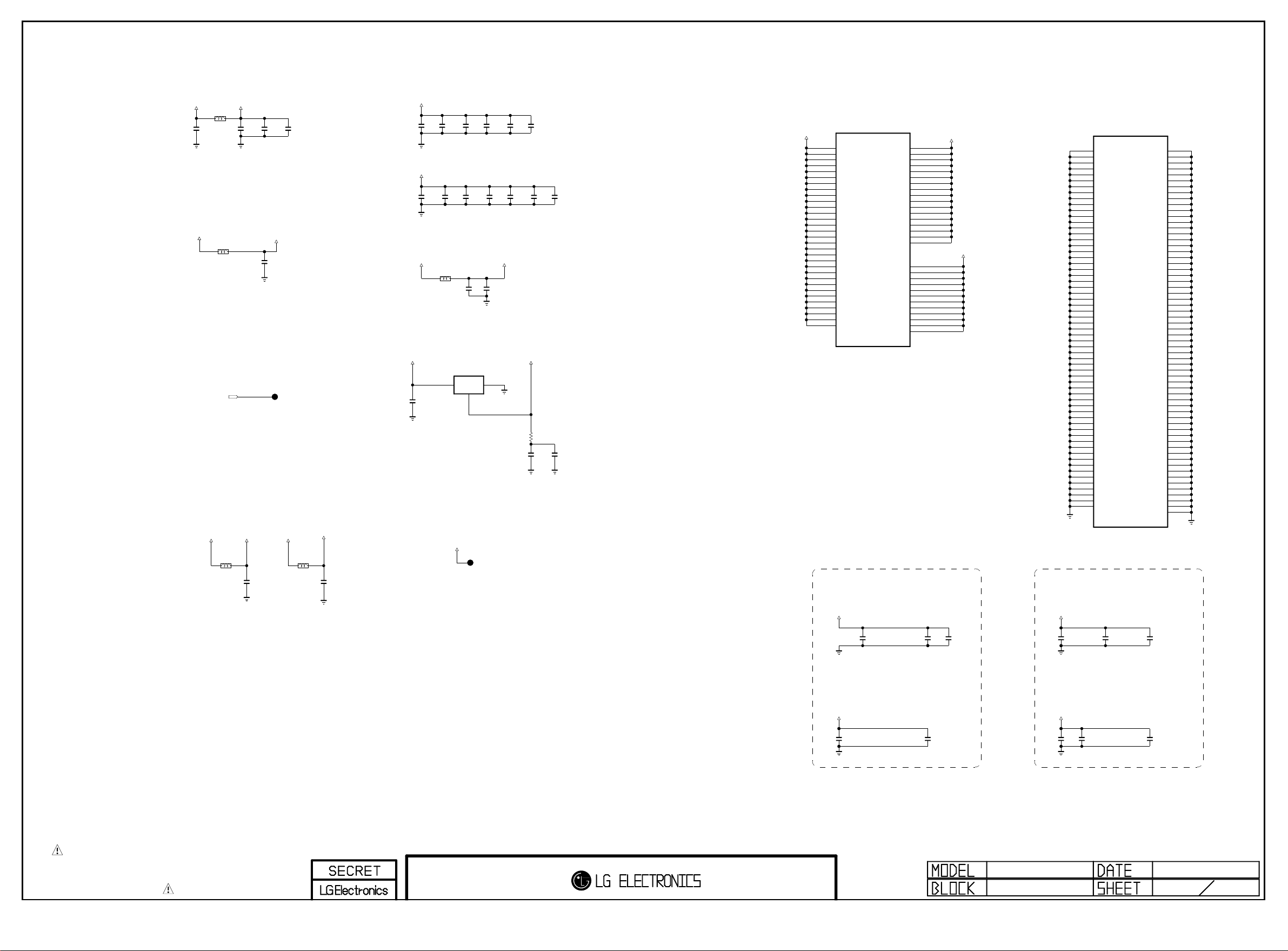
+3.3V_NORMAL
Copyright ⓒ 2012 LG Electronics. Inc. All right reserved.
Only for training and service purposes
LGE Internal Use Only
BLM18PG121SN1D
C500
10uF
VDD3V3
L500
L501
BLM18PG121SN1D
POWER_ON/OFF1
VDD3V3
C503
10uF
60mA
C510
0.1uF
AVDD_33SB
C501
0.1uF
TP500
C504
2.2uF
+1.2V_MTK_CORE
+1.2V_MTK_CORE
+1.2V_MTK_CORE +1.2V_MTK_AVDD
+5V_NORMAL
C526
10uF
10V
C506
C524
10uF
10uF
C539
C543
10uF
0.1uF
L502
BLM18PG121SN1D
AP1117E33G-13
5600mA
INADJ/GND
IC501
OUT
C505
10uF
C546
0.1uF
C525
10uF
C529
0.1uF
C548
0.1uF
C502
0.1uF
C532
0.1uF
C550
0.1uF
DAC_3V3
C535
0.1uF
C552
0.1uF
R500
1
C540
10uF
10V
C553
0.1uF
C544
0.1uF
16V
+1.2V_MTK_CORE
AA14
AB14
AC14
AC19
AC15
AC16
AA23
IC105
LGE2112
AR7
VCCK_43
AT7
VCCK_45
AU7
VCCK_47
AP8
VCCK_42
AR8
VCCK_44
AT8
VCCK_46
AU8
VCCK_48
AM7
VCCK_37
AN7
VCCK_39
AP7
VCCK_41
AM8
VCCK_38
AN8
VCCK_40
P14
VCCK_1
R14
VCCK_9
T14
VCCK_11
U14
VCCK_13
V14
VCCK_14
W14
VCCK_16
Y14
VCCK_18
VCCK_20
VCCK_22
VCCK_23
VCCK_28
P15
VCCK_2
VCCK_24
P16
VCCK_3
VCCK_25
V23
VCCK_15
W23
VCCK_17
Y23
VCCK_19
VCCK_21
VCCK_31
VCCK_32
VCCK_36
VCCK_8
VCCK_10
VCCK_12
VCCK_33
VCCK_30
VCCK_7
VCCK_29
VCCK_6
VCCK_27
VCCK_5
VCCK_26
VCCK_4
VCCK_34
VCCK_35
VCC3IO_B_4
VCC3IO_B_2
VCC3IO_B_1
VCC3IO_B_3
VCC3IO_A_5
VCC3IO_A_7
VCC3IO_A_6
VCC3IO_A_8
VCC3IO_A_3
VCC3IO_A_4
VCC3IO_A_2
VCC3IO_A_1
AC22
AC23
AD24
P23
R24
T24
AC24
AC21
P20
AC20
P19
AC18
P18
AC17
P17
AD18
AD23
AL9
AK10
AK9
AK11
H29
J29
H30
J30
G31
G32
F33
E34
+1.2V_MTK_CORE
VDD3V3
AA15
AB15
AA16
AB16
AA17
AB17
R2
R3
J4
R4
Y4
F5
J5
R5
Y5
W5
L7
M7
R7
AA5
AB5
K7
U7
W7
E9
E8
F9
G14
J6
R15
T15
U15
V15
W15
Y15
H11
R16
T16
U16
V16
W16
Y16
R17
T17
U17
V17
Y17
T18
V18
Y18
T19
V19
Y19
W17
R18
AB6
H19
H22
J11
J12
J22
DVSS_51
DVSS_52
DVSS_37
DVSS_53
DVSS_107
DVSS_20
DVSS_38
DVSS_54
DVSS_108
DVSS_95
DVSS_44
DVSS_46
DVSS_56
DVSS_120
DVSS_130
DVSS_43
DVSS_77
DVSS_97
DVSS_13
DVSS_12
DVSS_22
DVSS_28
DVSS_39
DVSS_57
DVSS_68
DVSS_78
DVSS_87
DVSS_99
DVSS_112
DVSS_122
DVSS_132
DVSS_34
DVSS_58
DVSS_69
DVSS_79
DVSS_88
DVSS_100
DVSS_113
DVSS_123
DVSS_133
DVSS_59
DVSS_70
DVSS_80
DVSS_89
DVSS_114
DVSS_71
DVSS_90
DVSS_115
DVSS_72
DVSS_91
DVSS_116
DVSS_101
DVSS_124
DVSS_134
DVSS_60
DVSS_131
DVSS_35
DVSS_36
DVSS_40
DVSS_41
DVSS_42
IC105
LGE2112
DVSS_55
DVSS_62
DVSS_73
DVSS_83
DVSS_92
DVSS_104
DVSS_117
DVSS_127
DVSS_137
DVSS_29
DVSS_63
DVSS_74
DVSS_84
DVSS_93
DVSS_105
DVSS_118
DVSS_128
DVSS_138
DVSS_64
DVSS_75
DVSS_85
DVSS_94
DVSS_106
DVSS_119
DVSS_129
DVSS_139
DVSS_65
DVSS_76
DVSS_86
DVSS_140
DVSS_96
DVSS_30
DVSS_27
DVSS_109
DVSS_17
DVSS_25
DVSS_45
DVSS_66
DVSS_7
DVSS_14
DVSS_8
DVSS_18
DVSS_26
DVSS_33
DVSS_136
DVSS_126
DVSS_49
DVSS_103
DVSS_82
DVSS_61
DVSS_110
DVSS_135
DVSS_125
DVSS_102
DVSS_81
DVSS_121
DVSS_47
DVSS_67
DVSS_98
DVSS_111
DVSS_11
DVSS_21
R6
R20
T20
U20
V20
W20
Y20
AA20
AB20
G16
R21
T21
U21
V21
W21
Y21
AA21
AB21
R22
T22
U22
V22
W22
Y22
AA22
AB22
R23
T23
U23
AB23
W6
G17
F25
Y6
E21
F21
L8
T7
D11
E11
D12
E22
F22
G25
AB19
AA19
P22
W19
U19
R19
Y7
AB18
AA18
W18
U18
AA7
N22
T8
W8
Y8
E7
F8
+3.3V_NORMAL
3.3V_EMMC
L504
BLM18PG121SN1D
C512
0.1uF
16V
+3.3V_NORMAL
EMMC_VCCQ
L506
BLM18PG121SN1D
C522
0.1uF
16V
LAN_JACK_POWER
TP501
DECAP FOR SOC (HIDDEN - UCC) DECAP FOR SOC (BOTTOM)
+1.2V_MTK_CORE
+1.5V_DDR
C508
0.1uF
C514
0.1uF
C520
0.1uF
C523
0.1uF
C527
0.1uF
+1.2V_MTK_CORE
C531
0.1uF
+1.5V_DDR
C533
0.1uF
C536
0.1uF
C537
0.1uF
C545
0.1uF
C547
0.1uF
THE SYMBOL MARK OF THIS SCHEMETIC DIAGRAM INCORPORATES
SPECIAL FEATURES IMPORTANT FOR PROTECTION FROM X-RADIATION.
FILRE AND ELECTRICAL SHOCK HAZARDS, WHEN SERVICING IF IS
ESSENTIAL THAT ONLY MANUFATURES SPECFIED PARTS BE USED FOR
THE CRITICAL COMPONENTS IN THE SYMBOL MARK OF THE SCHEMETIC.
MID_MAIN_3
2011.12.09
10
Page 24
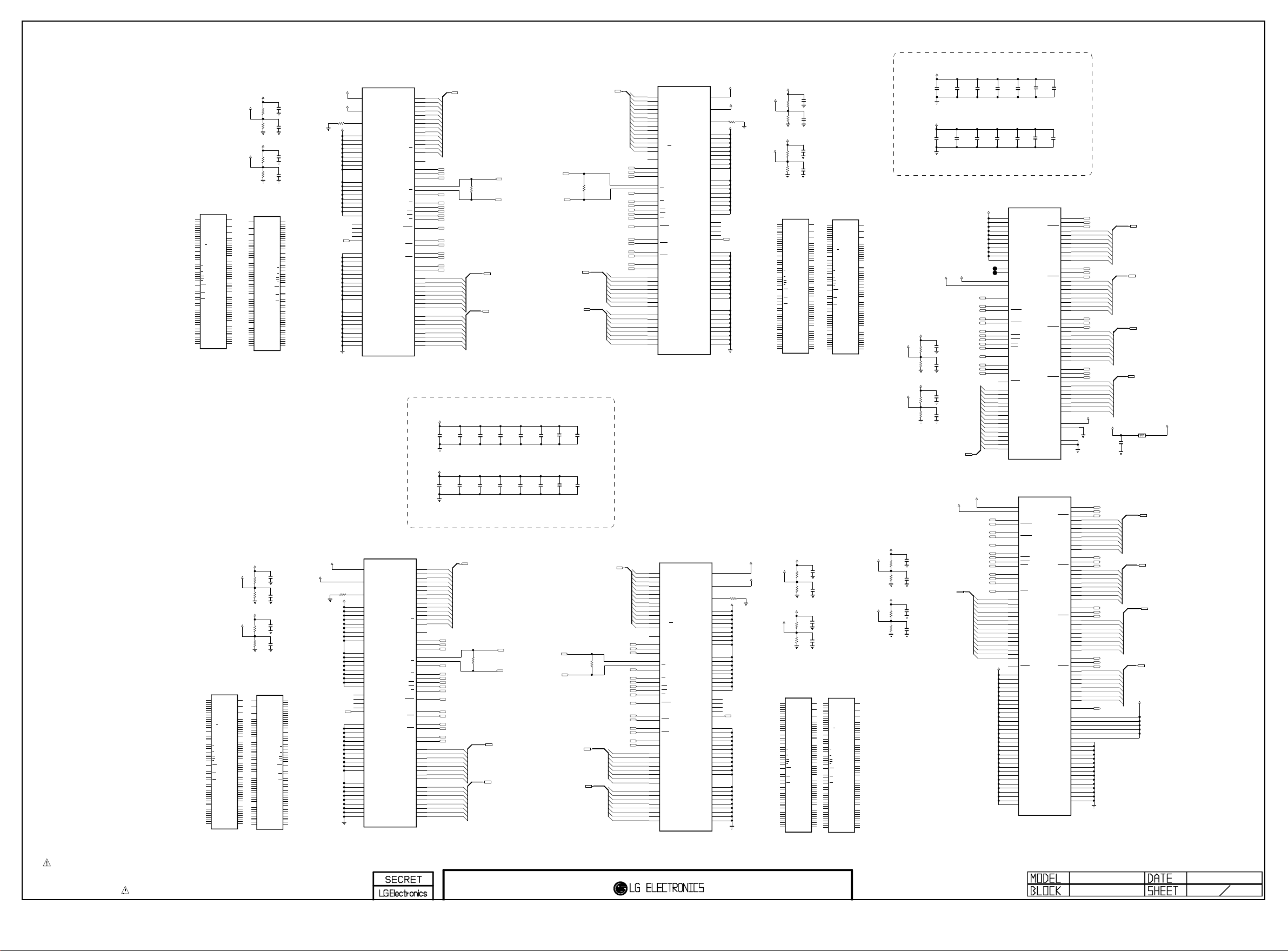
K4B2G1646C-HCK0
Copyright ⓒ 2012 LG Electronics. Inc. All right reserved.
Only for training and service purposes
LGE Internal Use Only
N3
A0
P7
A1
P3
A2
N2
A3
P8
A4
P2
A5
R8
A6
R2
A7
T8
A8
R3
A9
L7
A10/AP
R7
A11
N7
A12/BC
T3
A13
M7
NC_5
M2
BA0
N8
BA1
M3
BA2
J7
CK
K7
CK
K9
CKE
L2
CS
K1
ODT
J3
RAS
K3
CAS
L3
WE
T2
RESET
F3
DQSL
G3
DQSL
C7
DQSU
B7
DQSU
E7
DML
D3
DMU
E3
DQL0
F7
DQL1
F2
DQL2
F8
DQL3
H3
DQL4
H8
DQL5
G2
DQL6
H7
DQL7
D7
DQU0
C3
DQU1
C8
DQU2
C2
DQU3
A7
DQU4
A2
DQU5
B8
DQU6
A3
DQU7
IC701-*2
DDR_SS
K4B2G1646C-HCK0
N3
A0
P7
A1
P3
A2
N2
A3
P8
A4
P2
A5
R8
A6
R2
A7
T8
A8
R3
A9
L7
A10/AP
R7
A11
N7
A12/BC
T3
A13
M7
NC_5
M2
BA0
N8
BA1
M3
BA2
J7
CK
K7
CK
K9
CKE
L2
CS
K1
ODT
J3
RAS
K3
CAS
L3
WE
T2
RESET
F3
DQSL
G3
DQSL
C7
DQSU
B7
DQSU
E7
DML
D3
DMU
E3
DQL0
F7
DQL1
F2
DQL2
F8
DQL3
H3
DQL4
H8
DQL5
G2
DQL6
H7
DQL7
D7
DQU0
C3
DQU1
C8
DQU2
C2
DQU3
A7
DQU4
A2
DQU5
B8
DQU6
A3
DQU7
IC702-*2
RVREF_A
RVREF_B
+1.5V_DDR
+1.5V_DDR
R730
1K
1%
R731
1K
1%
R732
1K
1%
R733
1K
1%
+1.5V_DDR
+1.5V_DDR
C750
0.1uF
C745
0.1uF
RVREF_A
C746
0.1uF
C747
0.1uF
C748
0.1uF
C749
0.1uF
RVREF_B
ARA[0-14]
C752
0.1uF
C751
0.1uF
ARCKE
ARCLK1
/ARCLK1
ARCLK0
/ARCLK0
ARODT
/ARRAS
/ARCAS
/ARCS
/ARWE
ARREST
ARBA0
ARBA1
ARBA2
C754
0.1uF
C753
0.1uF
+1.5V_DDR
TP700
TP701
ARA[14]
ARA[13]
ARA[12]
ARA[11]
ARA[10]
ARA[9]
ARA[8]
ARA[7]
ARA[6]
ARA[5]
ARA[4]
ARA[3]
ARA[2]
ARA[1]
ARA[0]
C756
0.1uF
C755
0.1uF
C758
0.1uF
C757
0.1uF
LGE2112
AC1
DDRV_44
AC2
DDRV_45
A3
DDRV_1
A4
DDRV_2
B4
DDRV_5
C4
DDRV_8
D4
DDRV_10
B3
DDRV_4
C3
DDRV_7
AC3
DDRV_46
AC4
DDRV_47
G10
MEMTP
G9
MEMTN
G13
RVREF_B
G21
RVREF_A
F10
ARCKE
D9
ARCLK1
C9
ARCLK1
A20
ARCLK0
A21
ARCLK0
E18
ARODT
F17
ARRAS
E17
ARCAS
E16
ARCS
D14
ARWE
B14
ARRESET
A13
ARBA0
G11
ARBA1
D16
ARBA2
F18
ARCSX
C15
ARA14
A15
ARA13
F13
ARA12
C14
ARA11
F11
ARA10
E15
ARA9
D13
ARA8
B15
ARA7
E14
ARA6
F16
ARA5
E13
ARA4
B13
ARA3
A14
ARA2
F14
ARA1
F15
ARA0
IC105
1uF
C702
1uF
ARDQM0
ARDQS0
ARDQS0
ARDQ0
ARDQ1
ARDQ2
ARDQ3
ARDQ4
ARDQ5
ARDQ6
ARDQ7
ARDQM1
ARDQS1
ARDQS1
ARDQ8
ARDQ9
ARDQ10
ARDQ11
ARDQ12
ARDQ13
ARDQ14
ARDQ15
ARDQM2
ARDQS2
ARDQS2
ARDQ16
ARDQ17
ARDQ18
ARDQ19
ARDQ20
ARDQ21
ARDQ22
ARDQ23
ARDQM3
ARDQS3
ARDQS3
ARDQ24
ARDQ25
ARDQ26
ARDQ27
ARDQ28
ARDQ29
ARDQ30
ARDQ31
AVDD33_MEMPLL
AVSS33_MEMPLL
DVSS_50
DVSS_48
10uF
10V
C704
10uF
10V
C19
ARDQM0
C21
ARDQS0
B21
C23
B17
D23
C17
D24
C16
C24
D15
D21
B20
C20
A17
A23
D17
B23
D20
D22
D19
C22
A7
B9
A9
C12
D6
B12
C5
C13
A5
A12
B5
E10
C8
D8
C6
D10
D7
C11
C7
C10
B7
B10
N14
N15
R1
P21
/ARDQS0
ARDQM1
ARDQS1
/ARDQS1
ARDQM2
ARDQS2
/ARDQS2
ARDQM3
ARDQS3
/ARDQS3
AVDD3V3_MEMPLL
AVDD3V3_MEMPLL
0.1uF
ARDQ[0-7]
ARDQ[8-15]
ARDQ[16-23]
ARDQ[24-31]
+3.3V_NORMAL
L700
BLM18PG121SN1D
C700
C701
C703
IC701
H5TQ2G63BFR-PBC
R710
ARA[14]
A_RVREF4
A_RVREF1
+1.5V_DDR
A10/AP
A12/BC
RESET
N3
A0
P7
A1
P3
A2
N2
A3
P8
A4
P2
A5
R8
A6
R2
A7
T8
A8
R3
A9
ARA[10]
L7
ARA[11]
R7
A11
ARA[12]
N7
ARA[13]
T3
A13
M7
A15
M2
BA0
N8
BA1
M3
BA2
J7
CK
K7
CK
K9
CKE
L2
CS
K1
ODT
J3
RAS
K3
CAS
L3
WE
T2
F3
DQSL
G3
DQSL
C7
DQSU
B7
DQSU
E7
DML
D3
DMU
E3
DQL0
F7
DQL1
F2
DQL2
F8
DQL3
H3
DQL4
H8
DQL5
G2
DQL6
H7
DQL7
D7
DQU0
C3
DQU1
C8
DQU2
C2
DQU3
A7
DQU4
A2
DQU5
B8
DQU6
A3
DQU7
M8
VREFCA
H1
VREFDQ
1%
240
L8
ZQ
B2
VDD_1
D9
VDD_2
G7
VDD_3
K2
VDD_4
K8
VDD_5
N1
VDD_6
N9
VDD_7
R1
VDD_8
R9
VDD_9
A1
VDDQ_1
A8
VDDQ_2
C1
VDDQ_3
C9
VDDQ_4
D2
VDDQ_5
E9
VDDQ_6
F1
VDDQ_7
H2
VDDQ_8
H9
VDDQ_9
J1
NC_1
J9
NC_2
L1
NC_3
L9
NC_4
T7
NC_6
A9
VSS_1
B3
VSS_2
E1
VSS_3
G8
VSS_4
J2
VSS_5
J8
VSS_6
M1
VSS_7
M9
VSS_8
P1
VSS_9
P9
VSS_10
T1
VSS_11
T9
VSS_12
B1
VSSQ_1
B9
VSSQ_2
D1
VSSQ_3
D8
VSSQ_4
E2
VSSQ_5
E8
VSSQ_6
F9
VSSQ_7
G1
VSSQ_8
G9
VSSQ_9
DDR_HYNIX
+1.5V_DDR
A_RVREF1
C713
R706
0.1uF
1K
1%
R707
1K
C714
1%
0.1uF
+1.5V_DDR
A_RVREF4
M8
VREFCA
H1
VREFDQ
L8
ZQ
B2
VDD_1
D9
VDD_2
G7
VDD_3
K2
VDD_4
K8
VDD_5
N1
VDD_6
N9
VDD_7
R1
VDD_8
R9
VDD_9
A1
VDDQ_1
A8
VDDQ_2
C1
VDDQ_3
C9
VDDQ_4
D2
VDDQ_5
E9
VDDQ_6
F1
VDDQ_7
H2
VDDQ_8
H9
VDDQ_9
J1
NC_1
J9
NC_2
L1
NC_3
L9
NC_4
T7
NC_6
A9
VSS_1
B3
VSS_2
E1
VSS_3
G8
VSS_4
J2
VSS_5
J8
VSS_6
M1
VSS_7
M9
VSS_8
P1
VSS_9
P9
VSS_10
T1
VSS_11
T9
VSS_12
B1
VSSQ_1
B9
VSSQ_2
D1
VSSQ_3
D8
VSSQ_4
E2
VSSQ_5
E8
VSSQ_6
F9
VSSQ_7
G1
VSSQ_8
G9
VSSQ_9
IC701-*1
NT5CB128M16BP-DI
M8
VREFCA
H1
VREFDQ
L8
ZQ
B2
VDD_1
D9
VDD_2
G7
VDD_3
K2
VDD_4
K8
VDD_5
N1
VDD_6
N9
VDD_7
R1
VDD_8
R9
VDD_9
A1
VDDQ_1
A8
VDDQ_2
C1
VDDQ_3
C9
VDDQ_4
D2
VDDQ_5
E9
VDDQ_6
F1
VDDQ_7
H2
VDDQ_8
H9
VDDQ_9
J1
NC_1
J9
NC_2
L1
NC_3
L9
NC_4
T7
NC_7
A9
VSS_1
B3
VSS_2
E1
VSS_3
G8
VSS_4
J2
VSS_5
J8
VSS_6
M1
VSS_7
M9
VSS_8
P1
VSS_9
P9
VSS_10
T1
VSS_11
T9
VSS_12
B1
VSSQ_1
B9
VSSQ_2
D1
VSSQ_3
D8
VSSQ_4
E2
VSSQ_5
E8
VSSQ_6
F9
VSSQ_7
G1
VSSQ_8
G9
VSSQ_9
C715
R708
0.1uF
1K
1%
R709
1K
C716
1%
0.1uF
N3
A0
P7
A1
P3
A2
N2
A3
P8
A4
P2
A5
R8
A6
R2
A7
T8
A8
R3
A9
L7
A10/AP
R7
A11
N7
A12
T3
NC_6
M7
NC_5
M2
BA0
N8
BA1
M3
BA2
J7
CK
K7
CK
K9
CKE
L2
CS
K1
ODT
J3
RAS
K3
CAS
L3
WE
T2
RESET
F3
DQSL
G3
DQSL
C7
DQSU
B7
DQSU
E7
DML
D3
DMU
E3
DQL0
F7
DQL1
F2
DQL2
F8
DQL3
H3
DQL4
H8
DQL5
G2
DQL6
H7
DQL7
D7
DQU0
C3
DQU1
C8
DQU2
C2
DQU3
A7
DQU4
A2
DQU5
B8
DQU6
A3
DQU7
DDR_NANYA
ARA[0]
ARA[1]
ARA[2]
ARA[3]
ARA[4]
ARA[5]
ARA[6]
ARA[7]
ARA[8]
ARA[9]
ARBA0
ARBA1
ARBA2
ARCKE
/ARCS
ARODT
/ARRAS
/ARCAS
/ARWE
ARREST
ARDQS0
/ARDQS0
ARDQS1
/ARDQS1
ARDQM0
ARDQM1
ARA[0-13]
ARCLK0
R712
100
5%
/ARCLK0
ARDQ[0-7]
ARDQ[8-15]
ARCLK1
/ARCLK1
ARDQ[16-23]
ARDQ[24-31]
ARA[0-13]
R714
100
5%
/ARRAS
/ARCAS
ARREST
ARDQS2
/ARDQS2
ARDQS3
/ARDQS3
ARDQM2
ARDQM3
ARDQ[16]
ARDQ[17]
ARDQ[18]
ARDQ[19]
ARDQ[20]
ARDQ[21]
ARDQ[22]
ARDQ[23]
ARDQ[24]
ARDQ[25]
ARDQ[26]
ARDQ[27]
ARDQ[28]
ARDQ[29]
ARDQ[30]
ARDQ[31]
ARBA0
ARBA1
ARBA2
ARCKE
/ARCS
ARODT
/ARWE
ARA[0]
ARA[1]
ARA[2]
ARA[3]
ARA[4]
ARA[5]
ARA[6]
ARA[7]
ARA[8]
ARA[9]
ARA[10]
ARA[11]
ARA[12]
ARA[13]
IC703
H5TQ2G63BFR-PBC
N3
A0
P7
A1
P3
A2
N2
A3
P8
A4
P2
A5
R8
A6
R2
A7
T8
A8
R3
A9
L7
A10/AP
R7
A11
N7
A12/BC
T3
A13
M7
A15
M2
BA0
N8
BA1
M3
BA2
J7
CK
K7
CK
K9
CKE
L2
CS
K1
ODT
J3
RAS
K3
CAS
L3
WE
T2
RESET
F3
DQSL
G3
DQSL
C7
DQSU
B7
DQSU
E7
DML
D3
DMU
E3
DQL0
F7
DQL1
F2
DQL2
F8
DQL3
H3
DQL4
H8
DQL5
G2
DQL6
H7
DQL7
D7
DQU0
C3
DQU1
C8
DQU2
C2
DQU3
A7
DQU4
A2
DQU5
B8
DQU6
A3
DQU7
DDR_HYNIX
VREFCA
VREFDQ
VDD_1
VDD_2
VDD_3
VDD_4
VDD_5
VDD_6
VDD_7
VDD_8
VDD_9
VDDQ_1
VDDQ_2
VDDQ_3
VDDQ_4
VDDQ_5
VDDQ_6
VDDQ_7
VDDQ_8
VDDQ_9
VSS_1
VSS_2
VSS_3
VSS_4
VSS_5
VSS_6
VSS_7
VSS_8
VSS_9
VSS_10
VSS_11
VSS_12
VSSQ_1
VSSQ_2
VSSQ_3
VSSQ_4
VSSQ_5
VSSQ_6
VSSQ_7
VSSQ_8
VSSQ_9
A_RVREF2
M8
A_RVREF3
H1
1%
240
R716
L8
ZQ
+1.5V_DDR
B2
D9
G7
K2
K8
N1
N9
R1
R9
A1
A8
C1
C9
D2
E9
F1
H2
H9
J1
NC_1
J9
NC_2
L1
NC_3
L9
NC_4
T7
ARA[14]
NC_6
A9
B3
E1
G8
J2
J8
M1
M9
P1
P9
T1
T9
B1
B9
D1
D8
E2
E8
F9
G1
G9
A_RVREF2
A_RVREF3
+1.5V_DDR
+1.5V_DDR
IC703-*1
NT5CB128M16BP-DI
N3
A0
P7
A1
P3
A2
N2
A3
P8
A4
P2
A5
R8
A6
R2
A7
T8
A8
R3
A9
L7
A10/AP
R7
A11
N7
A12
T3
NC_6
M7
NC_5
M2
BA0
N8
BA1
M3
BA2
J7
CK
K7
CK
K9
CKE
L2
CS
K1
ODT
J3
RAS
K3
CAS
L3
WE
T2
RESET
F3
DQSL
G3
DQSL
C7
DQSU
B7
DQSU
E7
DML
D3
DMU
E3
DQL0
F7
DQL1
F2
DQL2
F8
DQL3
H3
DQL4
H8
DQL5
G2
DQL6
H7
DQL7
D7
DQU0
C3
DQU1
C8
DQU2
C2
DQU3
A7
DQU4
A2
DQU5
B8
DQU6
A3
DQU7
DDR_NANYA
C735
R720
0.1uF
1K
1%
R721
1K
C736
1%
0.1uF
C733
R718
0.1uF
1K
1%
R719
1K
C734
1%
0.1uF
IC703-*2
K4B2G1646C-HCK0
M8
VREFCA
H1
VREFDQ
L8
ZQ
B2
VDD_1
D9
VDD_2
G7
VDD_3
K2
VDD_4
K8
VDD_5
N1
VDD_6
N9
VDD_7
R1
VDD_8
R9
VDD_9
A1
VDDQ_1
A8
VDDQ_2
C1
VDDQ_3
C9
VDDQ_4
D2
VDDQ_5
E9
VDDQ_6
F1
VDDQ_7
H2
VDDQ_8
H9
VDDQ_9
J1
NC_1
J9
NC_2
L1
NC_3
L9
NC_4
T7
NC_7
A9
VSS_1
B3
VSS_2
E1
VSS_3
G8
VSS_4
J2
VSS_5
J8
VSS_6
M1
VSS_7
M9
VSS_8
P1
VSS_9
P9
VSS_10
T1
VSS_11
T9
VSS_12
B1
VSSQ_1
B9
VSSQ_2
D1
VSSQ_3
D8
VSSQ_4
E2
VSSQ_5
E8
VSSQ_6
F9
VSSQ_7
G1
VSSQ_8
G9
VSSQ_9
M8
N3
VREFCA
A0
P7
A1
P3
A2
H1
N2
VREFDQ
A3
P8
A4
P2
A5
L8
R8
ZQ
A6
R2
A7
T8
A8
B2
R3
VDD_1
A9
D9
L7
VDD_2
A10/AP
G7
R7
VDD_3
A11
K2
N7
VDD_4
A12/BC
K8
T3
VDD_5
A13
N1
VDD_6
N9
M7
VDD_7
NC_5
R1
VDD_8
R9
M2
VDD_9
BA0
N8
BA1
M3
BA2
A1
VDDQ_1
A8
J7
VDDQ_2
CK
C1
K7
VDDQ_3
CK
C9
K9
VDDQ_4
CKE
D2
VDDQ_5
E9
L2
VDDQ_6
CS
F1
K1
VDDQ_7
ODT
H2
J3
VDDQ_8
RAS
H9
K3
VDDQ_9
CAS
L3
WE
J1
NC_1
J9
T2
NC_2
RESET
L1
NC_3
L9
NC_4
T7
F3
NC_6
DQSL
G3
DQSL
A9
C7
VSS_1
DQSU
B3
B7
VSS_2
DQSU
E1
VSS_3
G8
E7
VSS_4
DML
J2
D3
VSS_5
DMU
J8
VSS_6
M1
E3
VSS_7
DQL0
M9
F7
VSS_8
DQL1
P1
F2
VSS_9
DQL2
P9
F8
VSS_10
DQL3
T1
H3
VSS_11
DQL4
T9
H8
VSS_12
DQL5
G2
DQL6
H7
DQL7
B1
VSSQ_1
B9
D7
VSSQ_2
DQU0
D1
C3
VSSQ_3
DQU1
D8
C8
VSSQ_4
DQU2
E2
C2
VSSQ_5
DQU3
E8
A7
VSSQ_6
DQU4
F9
A2
VSSQ_7
DQU5
G1
B8
VSSQ_8
DQU6
G9
A3
VSSQ_9
DQU7
DDR_SS
+1.5V_DDR
C707
C705
C718
0.1uF
C720
0.1uF
C722
0.1uF
C724
0.1uF
C726
0.1uF
C728
0.1uF
10uF
1uF
10V
+1.5V_DDR
C708
C719
0.1uF
BRA[0-13]
R713
100
5%
C721
0.1uF
BRDQ[0-7]
BRDQ[8-15]
0.1uF
/BRCLK0
BRCLK0
C725
0.1uF
C717
0.1uF
IC702
+1.5V_DDR
1%
240
H5TQ2G63BFR-PBC
M8
VREFCA
H1
VREFDQ
L8
ZQ
B2
VDD_1
D9
VDD_2
G7
VDD_3
K2
VDD_4
K8
VDD_5
N1
VDD_6
N9
VDD_7
R1
VDD_8
R9
VDD_9
A1
VDDQ_1
A8
VDDQ_2
C1
VDDQ_3
C9
VDDQ_4
D2
VDDQ_5
E9
VDDQ_6
F1
VDDQ_7
H2
VDDQ_8
H9
VDDQ_9
J1
NC_1
J9
NC_2
L1
NC_3
L9
NC_4
T7
NC_6
A9
VSS_1
B3
VSS_2
E1
VSS_3
G8
VSS_4
J2
VSS_5
J8
VSS_6
M1
VSS_7
M9
VSS_8
P1
VSS_9
P9
VSS_10
T1
VSS_11
T9
VSS_12
B1
VSSQ_1
B9
VSSQ_2
D1
VSSQ_3
D8
VSSQ_4
E2
VSSQ_5
E8
VSSQ_6
F9
VSSQ_7
G1
VSSQ_8
G9
VSSQ_9
DDR_HYNIX
A10/AP
A12/BC
RESET
BRA[0]
N3
A0
BRA[1]
P7
A1
BRA[2]
P3
A2
BRA[3]
N2
A3
BRA[4]
P8
A4
BRA[5]
P2
A5
BRA[6]
R8
A6
BRA[7]
R2
A7
BRA[8]
T8
A8
BRA[9]
R3
A9
BRA[10]
L7
BRA[11]
R7
A11
BRA[12]
N7
BRA[13]
T3
A13
M7
A15
M2
BA0
BA1
BA2
CK
CK
CKE
CS
ODT
RAS
CAS
WE
DQSL
DQSL
DQSU
DQSU
DML
DMU
DQL0
DQL1
DQL2
DQL3
DQL4
DQL5
DQL6
DQL7
DQU0
DQU1
DQU2
DQU3
DQU4
DQU5
DQU6
DQU7
BRBA0
N8
BRBA1
M3
BRBA2
J7
K7
K9
BRCKE
L2
/BRCS
K1
BRODT
J3
/BRRAS
K3
/BRCAS
L3
/BRWE
T2
BRREST
F3
BRDQS0
G3
/BRDQS0
C7
BRDQS1
B7
/BRDQS1
E7
BRDQM0
D3
BRDQM1
E3
F7
F2
F8
H3
H8
G2
H7
D7
C3
C8
C2
A7
A2
B8
A3
B_RVREF6
B_RVREF5
R711
B_RVREF5
+1.5V_DDR
C709
R702
0.1uF
1K
1%
R703
1K
C710
1%
0.1uF
+1.5V_DDR
B_RVREF6
M8
VREFCA
H1
VREFDQ
L8
ZQ
B2
VDD_1
D9
VDD_2
G7
VDD_3
K2
VDD_4
K8
VDD_5
N1
VDD_6
N9
VDD_7
R1
VDD_8
R9
VDD_9
A1
VDDQ_1
A8
VDDQ_2
C1
VDDQ_3
C9
VDDQ_4
D2
VDDQ_5
E9
VDDQ_6
F1
VDDQ_7
H2
VDDQ_8
H9
VDDQ_9
J1
NC_1
J9
NC_2
L1
NC_3
L9
NC_4
T7
NC_6
A9
VSS_1
B3
VSS_2
E1
VSS_3
G8
VSS_4
J2
VSS_5
J8
VSS_6
M1
VSS_7
M9
VSS_8
P1
VSS_9
P9
VSS_10
T1
VSS_11
T9
VSS_12
B1
VSSQ_1
B9
VSSQ_2
D1
VSSQ_3
D8
VSSQ_4
E2
VSSQ_5
E8
VSSQ_6
F9
VSSQ_7
G1
VSSQ_8
G9
VSSQ_9
DDR_SS
R704
1K
1%
R705
1K
1%
IC702-*1
NT5CB128M16BP-DI
M8
VREFCA
H1
VREFDQ
L8
ZQ
B2
VDD_1
D9
VDD_2
G7
VDD_3
K2
VDD_4
K8
VDD_5
N1
VDD_6
N9
VDD_7
R1
VDD_8
R9
VDD_9
A1
VDDQ_1
A8
VDDQ_2
C1
VDDQ_3
C9
VDDQ_4
D2
VDDQ_5
E9
VDDQ_6
F1
VDDQ_7
H2
VDDQ_8
H9
VDDQ_9
J1
NC_1
J9
NC_2
L1
NC_3
L9
NC_4
T7
NC_7
A9
VSS_1
B3
VSS_2
E1
VSS_3
G8
VSS_4
J2
VSS_5
J8
VSS_6
M1
VSS_7
M9
VSS_8
P1
VSS_9
P9
VSS_10
T1
VSS_11
T9
VSS_12
B1
VSSQ_1
B9
VSSQ_2
D1
VSSQ_3
D8
VSSQ_4
E2
VSSQ_5
E8
VSSQ_6
F9
VSSQ_7
G1
VSSQ_8
G9
VSSQ_9
DDR_NANYA
C711
0.1uF
C712
0.1uF
N3
A0
P7
A1
P3
A2
N2
A3
P8
A4
P2
A5
R8
A6
R2
A7
T8
A8
R3
A9
L7
A10/AP
R7
A11
N7
A12
T3
NC_6
M7
NC_5
M2
BA0
N8
BA1
M3
BA2
J7
CK
K7
CK
K9
CKE
L2
CS
K1
ODT
J3
RAS
K3
CAS
L3
WE
T2
RESET
F3
DQSL
G3
DQSL
C7
DQSU
B7
DQSU
E7
DML
D3
DMU
E3
DQL0
F7
DQL1
F2
DQL2
F8
DQL3
H3
DQL4
H8
DQL5
G2
DQL6
H7
DQL7
D7
DQU0
C3
DQU1
C8
DQU2
C2
DQU3
A7
DQU4
A2
DQU5
B8
DQU6
A3
DQU7
BRA[14]
C723
C727
0.1uF
BRCLK1
/BRCLK1
C706
1uF
BRDQ[16-23]
BRDQ[24-31]
10uF
10V
IC704
BRA[0-13]
R715
100
5%
/BRRAS
/BRCAS
BRREST
BRDQS2
/BRDQS2
BRDQS3
/BRDQS3
BRDQM2
BRDQM3
BRDQ[16]
BRDQ[17]
BRDQ[18]
BRDQ[19]
BRDQ[20]
BRDQ[21]
BRDQ[22]
BRDQ[23]
BRDQ[24]
BRDQ[25]
BRDQ[26]
BRDQ[27]
BRDQ[28]
BRDQ[29]
BRDQ[30]
BRDQ[31]
BRBA0
BRBA1
BRBA2
BRCKE
/BRCS
BRODT
/BRWE
BRA[0]
BRA[1]
BRA[2]
BRA[3]
BRA[4]
BRA[5]
BRA[6]
BRA[7]
BRA[8]
BRA[9]
BRA[10]
BRA[11]
BRA[12]
BRA[13]
N3
A0
P7
A1
P3
A2
N2
A3
P8
A4
P2
A5
R8
A6
R2
A7
T8
A8
R3
A9
L7
A10/AP
R7
A11
N7
A12/BC
T3
A13
M7
A15
M2
BA0
N8
BA1
M3
BA2
J7
CK
K7
CK
K9
CKE
L2
CS
K1
ODT
J3
RAS
K3
CAS
L3
WE
T2
RESET
F3
DQSL
G3
DQSL
C7
DQSU
B7
DQSU
E7
DML
D3
DMU
E3
DQL0
F7
DQL1
F2
DQL2
F8
DQL3
H3
DQL4
H8
DQL5
G2
DQL6
H7
DQL7
D7
DQU0
C3
DQU1
C8
DQU2
C2
DQU3
A7
DQU4
A2
DQU5
B8
DQU6
A3
DQU7
VREFCA
VREFDQ
VDDQ_1
VDDQ_2
VDDQ_3
VDDQ_4
VDDQ_5
VDDQ_6
VDDQ_7
VDDQ_8
VDDQ_9
VSS_10
VSS_11
VSS_12
VSSQ_1
VSSQ_2
VSSQ_3
VSSQ_4
VSSQ_5
VSSQ_6
VSSQ_7
VSSQ_8
VSSQ_9
VDD_1
VDD_2
VDD_3
VDD_4
VDD_5
VDD_6
VDD_7
VDD_8
VDD_9
VSS_1
VSS_2
VSS_3
VSS_4
VSS_5
VSS_6
VSS_7
VSS_8
VSS_9
NC_1
NC_2
NC_3
NC_4
NC_6
H5TQ2G63BFR-PBC
B_RVREF8
M8
B_RVREF7
H1
1%
240
R717
L8
ZQ
+1.5V_DDR
B2
D9
G7
K2
K8
N1
N9
R1
R9
A1
A8
C1
C9
D2
E9
F1
H2
H9
J1
J9
L1
L9
T7
BRA[14]
A9
B3
E1
G8
J2
J8
M1
M9
P1
P9
T1
T9
B1
B9
D1
D8
E2
E8
F9
G1
G9
DDR_HYNIX
B_RVREF7
B_RVREF8
+1.5V_DDR
+1.5V_DDR
NT5CB128M16BP-DI
N3
A0
P7
A1
P3
A2
N2
A3
P8
A4
P2
A5
R8
A6
R2
A7
T8
A8
R3
A9
L7
A10/AP
R7
A11
N7
A12
T3
NC_6
M7
NC_5
M2
BA0
N8
BA1
M3
BA2
J7
CK
K7
CK
K9
CKE
L2
CS
K1
ODT
J3
RAS
K3
CAS
L3
WE
T2
RESET
F3
DQSL
G3
DQSL
C7
DQSU
B7
DQSU
E7
DML
D3
DMU
E3
DQL0
F7
DQL1
F2
DQL2
F8
DQL3
H3
DQL4
H8
DQL5
G2
DQL6
H7
DQL7
D7
DQU0
C3
DQU1
C8
DQU2
C2
DQU3
A7
DQU4
A2
DQU5
B8
DQU6
A3
DQU7
DDR_NANYA
IC704-*1
C739
R724
0.1uF
1K
1%
R725
1K
C740
1%
0.1uF
C737
R722
0.1uF
1K
1%
R723
1K
C738
1%
0.1uF
IC704-*2
K4B2G1646C-HCK0
M8
N3
VREFCA
H1
VREFDQ
L8
ZQ
B2
VDD_1
D9
VDD_2
G7
VDD_3
K2
VDD_4
K8
VDD_5
N1
VDD_6
N9
VDD_7
R1
VDD_8
R9
VDD_9
A1
VDDQ_1
A8
VDDQ_2
C1
VDDQ_3
C9
VDDQ_4
D2
VDDQ_5
E9
VDDQ_6
F1
VDDQ_7
H2
VDDQ_8
H9
VDDQ_9
J1
NC_1
J9
NC_2
L1
NC_3
L9
NC_4
T7
NC_7
A9
VSS_1
B3
VSS_2
E1
VSS_3
G8
VSS_4
J2
VSS_5
J8
VSS_6
M1
VSS_7
M9
VSS_8
P1
VSS_9
P9
VSS_10
T1
VSS_11
T9
VSS_12
B1
VSSQ_1
B9
VSSQ_2
D1
VSSQ_3
D8
VSSQ_4
E2
VSSQ_5
E8
VSSQ_6
F9
VSSQ_7
G1
VSSQ_8
G9
VSSQ_9
VREFCA
A0
P7
A1
P3
A2
N2
VREFDQ
A3
P8
A4
P2
A5
R8
A6
R2
A7
T8
A8
R3
VDD_1
A9
L7
VDD_2
A10/AP
R7
VDD_3
A11
N7
VDD_4
A12/BC
T3
VDD_5
A13
VDD_6
M7
NC_5
VDD_7
VDD_8
M2
BA0
VDD_9
N8
BA1
M3
BA2
VDDQ_1
J7
CK
VDDQ_2
K7
CK
VDDQ_3
K9
VDDQ_4
CKE
VDDQ_5
L2
VDDQ_6
CS
K1
VDDQ_7
ODT
J3
VDDQ_8
RAS
K3
VDDQ_9
CAS
L3
WE
NC_1
T2
RESET
NC_2
NC_3
NC_4
F3
NC_6
DQSL
G3
DQSL
C7
VSS_1
DQSU
B7
VSS_2
DQSU
VSS_3
E7
VSS_4
DML
D3
VSS_5
DMU
VSS_6
E3
VSS_7
DQL0
F7
VSS_8
DQL1
F2
VSS_9
DQL2
F8
VSS_10
DQL3
H3
VSS_11
DQL4
H8
VSS_12
DQL5
G2
DQL6
H7
DQL7
VSSQ_1
D7
VSSQ_2
DQU0
C3
VSSQ_3
DQU1
C8
VSSQ_4
DQU2
C2
VSSQ_5
DQU3
A7
VSSQ_6
DQU4
A2
VSSQ_7
DQU5
B8
VSSQ_8
DQU6
A3
VSSQ_9
DQU7
DDR_SS
+1.5V_DDR
RVREF_C
C741
R726
0.1uF
1K
1%
R727
1K
C742
1%
0.1uF
+1.5V_DDR
RVREF_D
M8
H1
L8
ZQ
B2
D9
G7
K2
K8
N1
N9
R1
R9
A1
A8
C1
C9
D2
E9
F1
H2
H9
J1
J9
L1
L9
T7
A9
B3
E1
G8
J2
J8
M1
M9
P1
P9
T1
T9
B1
B9
D1
D8
E2
E8
F9
G1
G9
C743
R728
0.1uF
1K
1%
R729
1K
C744
1%
0.1uF
BRA[0-14]
RVREF_D
RVREF_C
BRCLK0
/BRCLK0
BRCLK1
/BRCLK1
BRCKE
BRODT
/BRRAS
/BRCAS
/BRCS
BRBA0
BRBA1
BRBA2
/BRWE
BRA[14]
BRA[13]
BRA[12]
BRA[11]
BRA[10]
BRA[9]
BRA[8]
BRA[7]
BRA[6]
BRA[5]
BRA[4]
BRA[3]
BRA[2]
BRA[1]
BRA[0]
+1.5V_DDR
IC105
LGE2112
P13
RVREF_C
V7
RVREF_D
F4
BRCLK0
F3
BRCLK0
V4
BRCLK1
V3
BRCLK1
P6
BRCKE
H6
BRODT
H4
BRRAS
H5
BRCAS
K3
BRCS
N1
BRBA0
P5
BRBA1
K4
BRBA2
L4
BRWE
L5
BRA14
M4
BRA13
N5
BRA12
M5
BRA11
P4
BRA10
M3
BRA9
L6
BRA8
L3
BRA7
N4
BRA6
K5
BRA5
N6
BRA4
N2
BRA3
M1
BRA2
N3
BRA1
K6
BRA0
G5
BRCSX
D5
DDRV_11
E5
DDRV_13
T5
DDRV_38
V5
DDRV_42
U5
DDRV_40
E6
DDRV_14
F6
DDRV_18
G6
DDRV_23
U6
DDRV_41
T6
DDRV_39
AC5
DDRV_48
F7
DDRV_19
G7
DDRV_24
AC6
DDRV_49
N7
DDRV_36
P7
DDRV_37
V6
DDRV_43
J10
DDRV_35
H10
DDRV_32
H13
DDRV_33
E20
DDRV_15
F20
DDRV_20
G20
DDRV_27
G15
DDRV_25
G18
DDRV_26
D25
DDRV_12
C25
DDRV_9
B25
DDRV_6
A25
DDRV_3
H7
DDRV_30
H8
DDRV_31
J8
DDRV_34
BRDQM0
BRDQS0
BRDQS0
BRDQ0
BRDQ1
BRDQ2
BRDQ3
BRDQ4
BRDQ5
BRDQ6
BRDQ7
BRDQM1
BRDQS1
BRDQS1
BRDQ8
BRDQ9
BRDQ10
BRDQ11
BRDQ12
BRDQ13
BRDQ14
BRDQ15
BRDQM2
BRDQS2
BRDQS2
BRDQ16
BRDQ17
BRDQ18
BRDQ19
BRDQ20
BRDQ21
BRDQ22
BRDQ23
BRDQM3
BRDQS3
BRDQS3
BRDQ24
BRDQ25
BRDQ26
BRDQ27
BRDQ28
BRDQ29
BRDQ30
BRDQ31
BRRESET
DDRV_16
DDRV_22
DDRV_29
DDRV_21
DDRV_28
DDRV_17
DVSS_15
DVSS_23
DVSS_1
DVSS_3
DVSS_5
DVSS_9
DVSS_16
DVSS_24
DVSS_31
DVSS_32
DVSS_19
DVSS_2
DVSS_4
DVSS_6
DVSS_10
G2
BRDQM0
E4
BRDQS0
E3
/BRDQS0
A1
J1
B2
J2
C2
K1
A2
K2
D1
BRDQM1
F1
BRDQS1
F2
/BRDQS1
J3
B1
H3
D3
G3
C1
G4
D2
Y1
BRDQM2
V2
BRDQS2
V1
/BRDQS2
T4
AB4
P2
AB3
P3
AB1
P1
AB2
U1
BRDQM3
W3
BRDQS3
W4
/BRDQS3
AA3
U4
AA4
T3
Y3
U3
Y2
U2
M2
BRREST
E23
F24
G24
F23
G23
E24
E12
F12
A18
B18
C18
D18
E19
F19
G19
G22
E25
A26
B26
C26
D26
BRDQ[0-7]
BRDQ[8-15]
BRDQ[16-23]
BRDQ[24-31]
+1.5V_DDR
THE SYMBOL MARK OF THIS SCHEMETIC DIAGRAM INCORPORATES
SPECIAL FEATURES IMPORTANT FOR PROTECTION FROM X-RADIATION.
FILRE AND ELECTRICAL SHOCK HAZARDS, WHEN SERVICING IF IS
ESSENTIAL THAT ONLY MANUFATURES SPECFIED PARTS BE USED FOR
THE CRITICAL COMPONENTS IN THE SYMBOL MARK OF THE SCHEMETIC.
2011.06.24
DDR ONE SIDE 12
Page 25
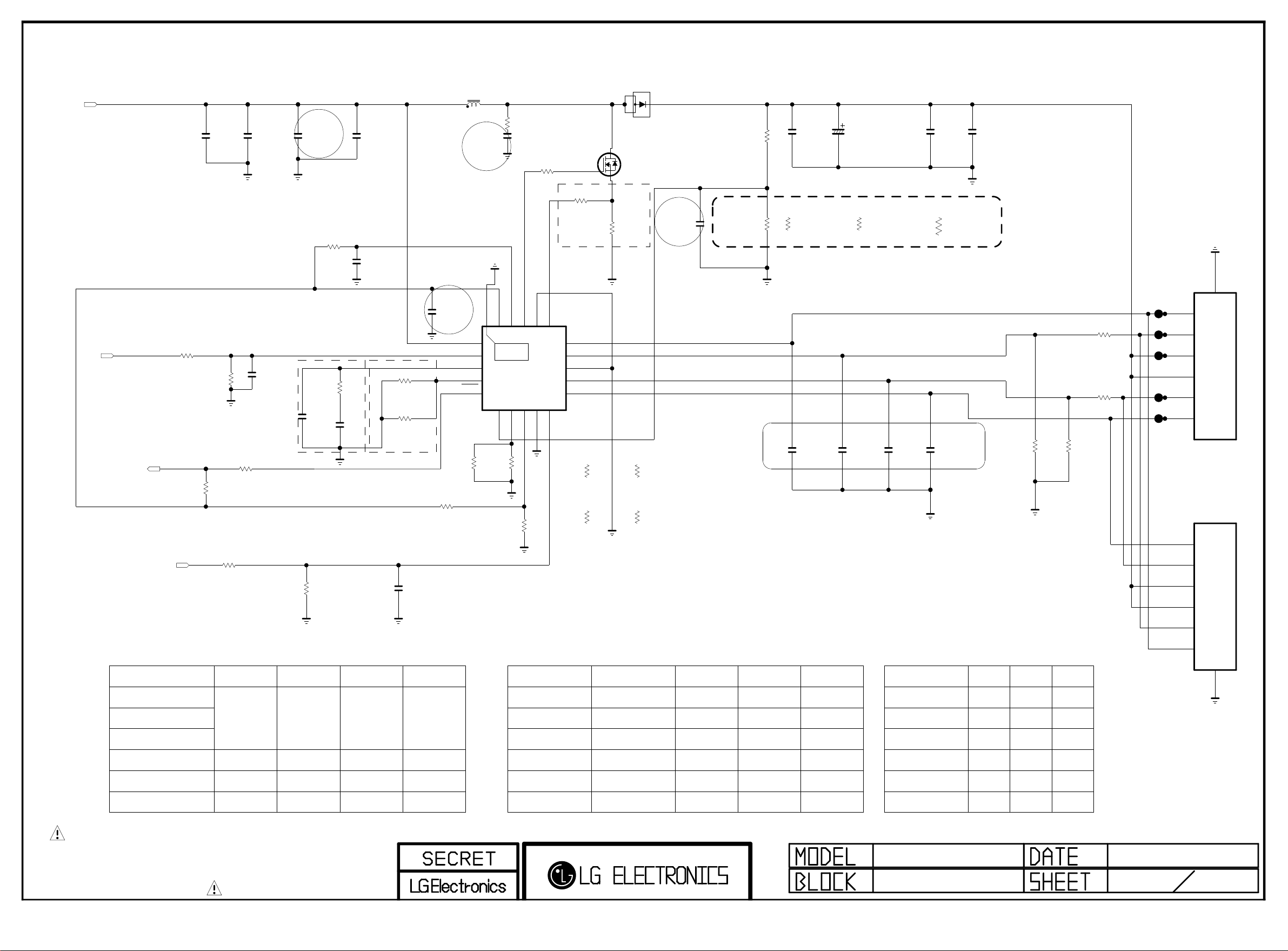
LED driver circuit for TN module
Copyright ⓒ 2012 LG Electronics. Inc. All right reserved.
Only for training and service purposes
LGE Internal Use Only
+24V_LED_driver
WLED_ENABLE
ERROR_OUT
PWM_DIM
21.5"
R10001
100
1/10W
R10002
10K
1/10W
OPT
21.5"
C10001
2.2uF
50V
R10004
100K
1/10W
21.5"
R10005
100
1/10W
21.5"
R10003
100
1/10W
21.5"
C10002
2.2uF
50V
close to IC10000
C104 : 10uF --> 2.2nF
C106 : 0.68uF --> 0.33uF
R111 : 470 --> 390
2010.02.07 for PQ/19V_LED
C10003
100pF
50V
21.5"
OPT
21.5"
C10005
0.1uF
50V
21.5"
R10007
4.7
1/10W
R10006
390
21.5"
C10006
2200pF
50V
R10024
3.9K
PWM_PULL_DOWN
1/10W
21.5"
C10007
0.33uF
50V
21.5"
21.5"
C10021
0.1uF
50V
C10008
0.1uF
50V
21.5"
2010.06.30. hwson
for thermal Issue
R113/R114
Operating Freq.
F=7.35x10^9/RT
close to IC10000
R10008
16K 1%
21.5"
R10009
51K 1%
OPT
21.5"
C10004
100pF
50V
L10001
33uH
must be modifed
21.5"
C10009
1uF
10V
COMP
FLT
R10011
47K
1/10W
1%
AUO_CPT
R10010
10K
1/8W
21.5"
21.5"
C10010
1000pF
50V
OPT
[EP]PGND/LEDGND
VCC
IN
20
1
THERMAL
EN
2
21
IC10000
3
4
5
R10013
51K
1/10W
5%
AUO_CPT
R10014
7.5K
1/8W
21.5"
MAX16814
6
OVP
RT
5.1
R10012
OPT
21.5"
R10015
12
1/10W
5%
PGND
NDRV
DRV
17
18
19
21.5"
7
8
SETI9SGND
RSDT
G
R10016
1/8W
3K
21.5"
R120 : 6.8K --> 3K
R121 : 0.03 --> 0.1
2010.06.30 HWSON
CS
OUT4
16
15
OUT3
14
LEDGND
13
OUT2
12
OUT1
11
10
DIM
R10011-*1
27K
1/10W
1%
LGD_21.5"
R10013-*1
27K
1/10W
1%
LGD_21.5"
21.5"
D10001
PDS5100H-13
21.5"
D
Q10001
AP18T10GH
S
21.5"
R10017
0.1
1%
R10011-*2
R10013-*2
OPT
C10011
1000pF
50V
must be modifed
39K
1/10W
1%
CMI
56K
1/10W
1%
CMI
21.5"
R10018
560K
1/10W
18.5"
R10019
1/10W
16K
21.5"
C10012
2.2uF
100V
21.5"
R10019-*1
11K
1/10W
C10013
1000pF
50V
21.5"
21.5"
C10014
10uF
100V
C10015
1000pF
50V
21.5"
CMI_21.5"
R10019-*2
16K
1/10W
ESD protection solution
C10017
1000pF
50V
21.5"
21.5"
C10018
2.2uF
100V
CMI_18.5"
R10019-*3
22K
1/10W
C10019
1000pF
50V
21.5"
C10020
2.2uF
100V
OPT
R10022
0
1/10W
5%
LGD_21.5"
wafer modify & resister add
NON_LGD
R10020
0
1/10W
5%
NON_LGD
R10021
0
1/10W
5%
R10023
0
1/10W
5%
LGD_21.5"
10031HR-H06
LGD_21.5"
7
6
5
4
3
2
1
P10000
NON_LGD
P10001
12507WR-06L
1
2
3
4
ILED = 1500/RSETI
R10011
R10013
OVP = 1.23*(1+R1/R2)
AUO_18.5_HD
AUO_21.5_FHD
60mA_Typ
63mA_Max
47Kohm
51Kohm
61.35mA 57.6
CPT_21.5_FHD
LGD_21.5_FHD 560Kohm
CMI_18.51_HD
CMI_21.6_FHD
110mA_Typ
120mA_Max
65mA_Typ
70mA_Max
65mA_Typ
70mA_Max
27Kohm
39Kohm
39Kohm
27Kohm
56Kohm
56Kohm
111.11mA
65.24mA
65.24mA
THE SYMBOL MARK OF THIS SCHEMETIC DIAGRAM INCORPORATES
SPECIAL FEATURES IMPORTANT FOR PROTECTION FROM X-RADIATION.
FILRE AND ELECTRICAL SHOCK HAZARDS, WHEN SERVICING IF IS
ESSENTIAL THAT ONLY MANUFATURES SPECFIED PARTS BE USED FOR
THE CRITICAL COMPONENTS IN THE SYMBOL MARK OF THE SCHEMETIC.
Module
AUO_18.5
AUO_21.5
CPT_21.5
LGD_21.5
CMI_18.51
CMI_21.6
Vs specModule
34.0V_Typ
36.0V_Max
52.8V_Typ
57.6V_Max
52.0V_Typ
57.6V_Max
51.2V_Typ
56.0V_Max
24.8V_Typ
27.2V_Max
37.8V_Typ
40.8V_Max
R10018
560Kohm
560Kohm
560Kohm
560Kohm
560Kohm
Forward voltage spec.
R10019
16Kohm
11Kohm 48.0
11Kohm CPT_21.5
Remark
44.28V
63.85V
63.85V
63.85V11Kohm
22Kohm
16Kohm
32.54V
44.28V
ModuleILED spec
AUO_18.5
AUO_21.5
LGD_21.5
CMI_18.51
CMI_21.6
minRemark
30.0
46.4
-
-
33.6
S7LR SMALL TN
LED driver
34.0
52.8
52.0
51.2
24.8
37.8
5
6
7
MaxTyp
36.0
57.6
56.0
27.2
40.8
2011.05.09
29
Page 26

Renesas MICOM
Copyright ⓒ 2012 LG Electronics. Inc. All right reserved.
Only for training and service purposes
LGE Internal Use Only
For Debug
+3.5V_ST
MICOM_DEBUG
P3000
12507WS-12L
1
2
3
4
5
6
7
8
9
10
11
12
13
GP4 High/MID Power SEQUENCE
POWER_ON/OFF1
POWER_ON/OFF2_1
POWER_ON/OFF2_2
POWER_ON/OFF2_3
POWER_ON/OFF2_4
SOC_RESET
MICOM MODEL OPTION
MICOM_MHL
MICOM_GED
R3016 10K
R3020 10K
MICOM_GP4_10PIN
R3030 10K
Don’t remove R3014,
Not making P40 floated
R3014 1K
R3011 10K
MICOM_DEBUG
+3.5V_ST
MICOM_PDP
R3007 10K
R3005 10K
MICOM_JAPAN
MICOM_TOUCH_KEY
R3009 10K
MICOM_DEBUG
MICOM_RESET
R3005-*1
R3012 10K
MICOM_OLED_MAIN
MICOM_LOGO_LIGHT
R3005-*2
56K
MICOM_OLED_FRC
MODEL1_OPT_0
MODEL1_OPT_1
MODEL1_OPT_2
MODEL1_OPT_3
MODEL1_OPT_4
MODEL1_OPT_5
MODEL1_OPT_6
+3.3V_NORMAL
R3035
4.7K
MICOM MODEL OPTION
POWER_ON/OFF2_3
I2C_SCL3
I2C_SDA3
AMP_RESET_N
PANEL_CTL
MODEL1_OPT_5
HDMI_CEC
POWER_ON/OFF2_2
POWER_ON/OFF2_3
EEPROM_SDA
EEPROM_SCL
MODEL1_OPT_6
AMP_RESET_BY_MICOM
IR
+3.5V_ST
R3018
3.3K
+3.3V_NORMAL
R3032
10K
R3033
10K
R3003 22
AMP_RESET_BY_MICOM
P31/TI03/TO03/INTP4
P75/KR5/INTP9/SCK01/SCL01
P74/KR4/INTP8/SI01/SDA01
P71/KR1/SI21/SDA21
P70/KR0/SCK21/SCL21
P30/INTP3/RTC1HZ/SCK11/SCL11
R3019
3.3K
FLG_POD_DR
POD_WAKEUP_N
/RST_DIIVA
/RST_DIIVA
POD_WAKEUP_N
FLG_POD_DR
for DiiVA
+3.5V_ST
C3000
0.1uF
P60/SCLA0
P61/SDAA0
P62
P63
P73/KR3/SO01
P72/KR2/SO21
R3002 22
MICOM_DIIVA
R3001 22
MICOM_DIIVA
VDD
48
1
2
3
4
5
6
7
8
9
10
11
12
13
GND
VSS
47
14
C3001 0.47uF
P121/X1
REGC
46
15
OPT
8pF
C3002
C3003 8pF
X3000
32.768KHz
R3023
4.7M
OPT
P124/XT2/EXCLKS
P123/XT1
P137/INTP0
P122/X2/EXCLK
41
42
43
44
45
IC3000
R5F100GEAFB
MICOM
16
17
18
19
20
MICOM_DEBUG
LOGO_LIGHT
MICOM_RESET
MICOM_DIIVA
R3024 22
P41/TI07/TO07
P40/TOOL0
RESET
38
39
40
21
22
23
P146
10K
R3000
LOGO_LIGHT
+3.5V_ST
R3025 22
C3004
0.1uF
16V
P120/ANI19
37
36
35
34
33
32
31
30
29
28
27
26
25
24
12V_EXT_PWR_DET
HDMI_WAUP:HDMI_INIT
10K
MICOM_RESET_SW
SW3000
R3026
JTP-1127WEM
12
4 3
R3027
270K
OPT
P140/PCLBUZ0/INTP6
P00/TI00/TXD1
P01/TO00/RXD1
For Japan:LNB_INIT
P130
P20/ANI0/AVREFP
P21/ANI1/AVREFM
P22/ANI2
P23/ANI3
P24/ANI4
P25/ANI5
P26/ANI6
P27/ANI7
POWER_ON/OFF2_4
RL_ON
SCART_MUTE
POWER_ON/OFF2_4
EXT_AMP_MUTE
EXT_AMP_RESET
COMMERCIAL_12V_CTL
12V_EXT_PWR_DET
SCART_MUTE
KEY2
KEY1
MODEL1_OPT_2
MODEL1_OPT_1
MODEL1_OPT_0
MODEL1_OPT_4
MODEL1_OPT_3
+3.3V_NORMAL
+3.3V_NORMAL
R3036
10K
OPT
R3037
10K
OPT
POWER_ON/OFF2_1
SIDE_HP_MUTE
10
P147/ANI18
P10/SCK00/SCL00
/ OLED
LOGO_LIGHT
JAPAN
TOUCH_KEY
PDP
IR Wafer
10Pin
(GP4_TOOL)
MHLMODEL_OPT_5
GEDMODEL_OPT_6
For LM86
For JAPAN
For Sample Set
GP4_HIGH
P17/TI02/TO02
P51/INTP2/SO11
P50/INTP1/SI11/SDA11
P16/TI01/TO01/INTP5
P13/TXD2/SO20
P14/RXD2/SI20/SDA20
P12/SO00/TXD0/TOOLTXD
P15/PCLBUZ1/SCK20/SCL20
P11/SI00/RXD0/TOOLRXD/SDA00
R30 22 1 0K
MODEL_OPT_0
MODEL_OPT_1
22K
MODEL_OPT_2
MODEL_OPT_3
MODEL_OPT_4
NON LOGO_LIGHT
NON JAPAN
TACT_KEY
LCD
IR Wafer
12/15Pin
(GP3_Soft touch)
NON_MHL
NON_GED
R3006 10K
R3008 10K
R3010 10K
R3021 10K
R3017 10K
MICOM_NON_MHL
MICOM_NON_GED
R3031 10K
MICOM_LCD/OLED
MICOM_GP3_12/15PIN
MICOM_TACT_KEY
R3013 10K
MICOM_NON_JAPAN
MICOM_NON_LOGO_LIGHT
THE SYMBOL MARK OF THIS SCHEMETIC DIAGRAM INCORPORATES
SPECIAL FEATURES IMPORTANT FOR PROTECTION FROM X-RADIATION.
FILRE AND ELECTRICAL SHOCK HAZARDS, WHEN SERVICING IF IS
ESSENTIAL THAT ONLY MANUFATURES SPECFIED PARTS BE USED FOR
THE CRITICAL COMPONENTS IN THE SYMBOL MARK OF THE SCHEMETIC.
Eye Sensor Option
MODEL_OPT_4
MODEL_OPT_2
0
1
0
N/A
CM3231_CAPELLA
(GP3 Soft touch) (GP4 Soft touch)
1
MC8101_ABOV
(TACT_KEY)
CM3231_CAPELLA
POWER_ON/OFF1
+3.3V_NORMAL
R3034
4.7K
OPT
POWER_DET
COMMERCIAL_12V_CTL
LED_B/GP4_LED_R
B
INV_CTL
SOC_RESET
C
Q3000
MMBT3904(NXP)
EDID_WP
E
SOC_TX
SOC_RX
AMP_MUTE
EXT_AMP_MUTE
EDID_WP
EXT_AMP_RESET
CEC_REMOTE
MICOM
D3000
BAT54_SUZHO
D
For CEC
R3028
27K
G
Q3001-*1
SI1012CR-T1-GE3
S
HDMI_CEC_FET_VISHAY
+3.5V_ST
G
D
Q3001
RUE003N02
HDMI_CEC_FET_ROHM
R3029
120K
S
HDMI_CEC
2011.12.12
30
Page 27

SHIELD
Copyright ⓒ 2012 LG Electronics. Inc. All right reserved.
Only for training and service purposes
LGE Internal Use Only
GND
20
EAG59023302
YKF45-7058V
JK3301
19
18
17
16
15
14
13
12
11
10
9
8
7
6
5
4
3
2
1
HP_DET
5V
GND
DDC_DATA
DDC_CLK
NC
CE_REMOTE
CK-
CK_GND
CK+
D0-
D0_GND
D0+
D1-
D1_GND
D1+
D2-
D2_GND
D2+
5V_HDMI_4_JACK
R3308 100
R3309 100
R33 00 0
D3005
RCLAMP0544T.TCT
6.5VTO11.0V
1 8
2 7
3 6
4 5
9
D3004
RCLAMP0544T.TCT
6.5VTO11.0V
1 8
2 7
3 6
4 5
9
Q3301
R3307
100K
MMBT3904(NXP)
CEC_REMOTE
CK-_HDMI4_JACK
CK+_HDMI4_JACK
D0-_HDMI4_JACK
D0+_HDMI4_JACK
D1-_HDMI4_JACK
D1+_HDMI4_JACK
D2-_HDMI4_JACK
D2+_HDMI4_JACK
R3310
1K
C
B
E
DDC_SDA_4_JACK
DDC_SCL_4_JACK
R3312
4.7K
R3311
1K
UI : HDMI1
HDMI_HPD_4_JACK
HDMI_ARC
BODY_SHIELD
20
HP_DET
19
5V
18
GND
17
DDC_DATA
16
DDC_CLK
15
NC
14
CE_REMOTE
13
CK-
12
CK_GND
11
CK+
10
D0-
9
D0_GND
8
EAG62611201
7
6
5
4
3
2
1
JK3303
RSD-105156-100
D0+
D1-
D1_GND
D1+
D2-
D2_GND
D2+
22_26LS35_HDMI_SIDE_JACK
5V_HDMI_3_JACK
R3327
100K
MMBT3904(NXP)
R3328 100
R3329 100
C
Q3303
E
DDC_SDA_3_JACK
DDC_SCL_3_JACK
CEC_REMOTE
CK-_HDMI3_JACK
CK+_HDMI3_JACK
D0-_HDMI3_JACK
D0+_HDMI3_JACK
D1-_HDMI3_JACK
D1+_HDMI3_JACK
D2-_HDMI3_JACK
D2+_HDMI3_JACK
R3330
1K
R3331
1K
B
UI : HDMI3
R3336
4.7K
32LS35_HDMI_SIDE_JACK
JK3303-*1
51U019S-312HFN-E-R-E-LG
20
BODY_SHIELD
HDMI_HPD_3_JACK
TMDS_DATA2+
1
TMDS_DATA2_SHIELD
2
TMDS_DATA2-
3
TMDS_DATA1+
4
TMDS_DATA1_SHIELD
5
TMDS_DATA1-
6
TMDS_DATA0+
7
TMDS_DATA0_SHIELD
8
TMDS_DATA0-
9
TMDS_CLK+
10
TMDS_CLK_SHIELD
11
TMDS_CLK-
12
CEC
13
RESERVED
14
SCL
15
SDA
16
DDC/CEC_GND
17
VDD[+5V]
18
HOT_PLUG_DETECT
19
5V_HDMI_3_JACK
C3302
0.1uF
16V
R3337
47K
+5V_NORMAL
A1CA2
SDS2838F
D3302
R3339
47K
DDC_SCL_3_JACK
DDC_SDA_3_JACK
SHIELD
20
EAG59023302
JK3302
YKF45-7058V
19
18
17
16
15
14
13
12
11
10
9
8
7
6
5
4
3
2
1
HP_DET
5V
GND
DDC_DATA
DDC_CLK
NC
CE_REMOTE
CK-
CK_GND
CK+
D0-
D0_GND
D0+
D1-
D1_GND
D1+
D2-
D2_GND
D2+
D3007
RCLAMP0544T.TCT
6.5VTO11.0V
1 8
2 7
3 6
4 5
9
D3006
RCLAMP0544T.TCT
6.5VTO11.0V
1 8
2 7
3 6
4 5
9
5V_HDMI_2_JACK
R3313
100K
MMBT3904(NXP)
R3314 100
R3315 100
CEC_REMOTE
CK-_HDMI2_JACK
CK+_HDMI2_JACK
D0-_HDMI2_JACK
D0+_HDMI2_JACK
D1-_HDMI2_JACK
D1+_HDMI2_JACK
D2-_HDMI2_JACK
D2+_HDMI2_JACK
C
Q3302
E
DDC_SDA_2_JACK
DDC_SCL_2_JACK
R3316
1K
R3318
4.7K
R3317
1K
B
UI : HDMI2
HDMI_HPD_2_JACK
5V_HDMI_2_JACK
C3301
0.1uF
16V
R3324
47K
+5V_NORMAL
A1CA2
SDS2838F
D3301
R3326
47K
DDC_SCL_2_JACK
DDC_SDA_2_JACK
5V_HDMI_4_JACK
C3303
0.1uF
16V
R3338
47K
+5V_NORMAL
A1CA2
SDS2838F
D3303
R3340
47K
DDC_SCL_4_JACK
DDC_SDA_4_JACK
THE SYMBOL MARK OF THIS SCHEMETIC DIAGRAM INCORPORATES
SPECIAL FEATURES IMPORTANT FOR PROTECTION FROM X-RADIATION.
FILRE AND ELECTRICAL SHOCK HAZARDS, WHEN SERVICING IF IS
ESSENTIAL THAT ONLY MANUFATURES SPECFIED PARTS BE USED FOR
THE CRITICAL COMPONENTS IN THE SYMBOL MARK OF THE SCHEMETIC.
HDMI 4
2011.07.22
33
Page 28

RGB/ PC AUDIO/ SPDIF/ D5(COMPONENT)
Copyright ⓒ 2012 LG Electronics. Inc. All right reserved.
Only for training and service purposes
LGE Internal Use Only
RGB PC
DSUB_VSYNC
DSUB_HSYNC
DSUB_B+
DSUB_G+
DSUB_R+
D3904
30V
D3905
30V
+5V_NORMAL
R3916 22
R3917 22
D3913
ADUC 5S 02 0R5L
5.5V
OPT
EDID_WP
RGB_DDC_SCL
RGB_DDC_SDA
+3.3V_NORMAL
R3919
10K
D3914
5.5V
OPT
COMPONENT/D5
JK3900
SP01-SC-002
1
3
5
7
8
10
12
14
15
DSUB_DET
R39201K
Y
Y_GND
2
Pb
Pb_GND
4
Pr
Pr_GND
6
.
LINE1
LINE2
9
.
LINE3
11
PLUG_GND
.
13
PLUG
.
D3903
5.6V
OPT
D3903-*1
5.6V
ESD_MTK
R3902
56K
1%
+3.3V_NORMAL
R3903
100K
1%
R3904
10K R3905
1K
C3904
100pF
50V
C3908
1000pF
50V
COMP1_DET
C3914
18pF
RGB_5V
R3914
2.7K
C3915
18pF
50V
50V
R3915
2.7K
D3911
MMBD6100
C
A2
A1
R3918
10K
RGB_EDID
D3912
ADUC 5S 02 0R5L
5.5V
OPT
RGB_5V
IC3900
M24C02-RMN6T
E0
E1
E2
VSS
VCC
8
1
WC
2
7
RGB_EDID
SCL
3
6
SDA
4
5
COMP1_Y
11:D3
COMP1_Pb
11:D3
COMP1_Pr
11:D3
COMP1_DET
9:G5
PC AUDIO
JK3902
PEJ027-04
E_SPRING
3
T_TERMINAL1
6A
B_TERMINAL1
7A
R_SPRING
4
T_SPRING
5
B_TERMINAL2
7B
T_TERMINAL2
6B
OPT
D3907
5.6V
OPT
D3906
5.6V
D3907-*1
5.6V
ESD_MTK
D3906-*1
5.6V
ESD_MTK
PC_R_IN
PC_L_IN
Closed to JACK
RED2GREEN3BLUE4GND_15DDC_GND
RED_GND7GREEN_GND8BLUE_GND9NC10SYNC_GND
GND_212DDC_DATA13H_SYNC14V_SYNC15DDC_CLOCK
11
6
1
P3900
SPG09-DB-010
SPDIF OUT
SPDIF_OUT
SHILED
16
OPT
R3901
2.7K
R3900
33
D3900
5.6V
OPT
ADMC 5M 02 200L
D3900-*1
5.5V
ADUC 5S 02 0R5L
ESD_MTK
+3.3V_NORMAL
C3900
0.1uF
16V
JST1223-001
GND
VCC
VINPUT
JK3901
1
2
3
Fib er Opt ic
4
FIX_POLE
THE SYMBOL MARK OF THIS SCHEMETIC DIAGRAM INCORPORATES
SPECIAL FEATURES IMPORTANT FOR PROTECTION FROM X-RADIATION.
FILRE AND ELECTRICAL SHOCK HAZARDS, WHEN SERVICING IF IS
ESSENTIAL THAT ONLY MANUFATURES SPECFIED PARTS BE USED FOR
THE CRITICAL COMPONENTS IN THE SYMBOL MARK OF THE SCHEMETIC.
Page 29

RS232C
Copyright ⓒ 2012 LG Electronics. Inc. All right reserved.
Only for training and service purposes
LGE Internal Use Only
0.1uF
C40000.1uF
C4001
C40020.1uF
C40030.1uF
DOUT2
RIN2
C1+
V+
C1-
C2+
C2-
V-
IC4000
MAX3232CDR
1
2
3
4
5
6
7
8
EAN41348201
12V_COMMERCIAL_OUT
12V 1A FOR COMMERCIAL(RS-232C POWER)
12V_COMMERCIAL_OUT
10
5
9
P4000
4
8
3
7
2
6
1
R4001
4.7K
OPT
IR_OUT
D4001
20V
OPT
100
100
R4002
R4003
+3.5V_ST
R4006
10K
FOR COMMERCIAL
JP4000
JP4001
SPG09-DB-009
SOC_RX
+3.5V_ST
VCC
16
GND
15
DOUT1
14
RIN1
13
ROUT1
12
DIN1
11
DIN2
10
ROUT2
9
+3.5V_ST
R4000
4.7K
OPT
D4000
20V
OPT
AV1 & D5 Audio
JK4000
PPJ234-03
6E
[YL ]E- LUG
[YL]O-SPRING
5E
[YL]CONTACT
4E
[WH2]O-SPRING
5D
[RD2]CONTACT
4C
[RD2]O-SPRING
5C
[RD2]E-LUG-S
7C
[WH1]O-SPRING
5B
[WH1]E-LUG-S
7B
[RD1]CONTACT
4A
[RD1]O-SPRING
5A
[RD1]E-LUG
6A
OPT
D4002
5.6V
D4003
5.6V
D4004
D4005
OPT
5.6V
5.6V
+3.3V_NORMAL
R4007
10K
AV1_CVBS_DET
D4002-*1
5.6V
ESD_MTK
D4003-*1
5.6V
ESD_MTK
OPT
OPT
D4004-*1
5.6V
ESD_MTK
D4005-*1
5.6V
ESD_MTK
AV1_CVBS_IN
AV1_L_IN
AV1_R_IN
EARPHONE
HP_LOUT
HP_ROUT
HP_DET
D4006-*1
5.6V
ESD_MTK_HP_OUT
+3.3V_NORMAL
R4010
10K
OPT
D4006
5.6V
SOC_TX
JK4001
KJA-PH-0-0177
5GND
4L
3DETECT
1R
EAG61030001
22_26LS35_HP_OUT_JACK
JK4001-*1
PEJ031-01
5GND
4L
3DETECT
1R
EAG61030005
32LS35_HP_OUT_JACK
THE SYMBOL MARK OF THIS SCHEMETIC DIAGRAM INCORPORATES
SPECIAL FEATURES IMPORTANT FOR PROTECTION FROM X-RADIATION.
FILRE AND ELECTRICAL SHOCK HAZARDS, WHEN SERVICING IF IS
ESSENTIAL THAT ONLY MANUFATURES SPECFIED PARTS BE USED FOR
THE CRITICAL COMPONENTS IN THE SYMBOL MARK OF THE SCHEMETIC.
Page 30

D4105-*3
Copyright ⓒ 2012 LG Electronics. Inc. All right reserved.
Only for training and service purposes
LGE Internal Use Only
CDS2C20GTHB
20V
DEV_EPCOS_20V
D4106-*3
CDS2C20GTHB
20V
DEV_EPCOS_20V
IR
IR & KEY
COMMERCIAL
MMBT3904(NXP)
COMMERCIAL_IR
Q4100
+3.5V_ST
R4101
1K
IR_BYPASS
COMMERCIAL_IR
C
B
E
COMMERCIAL_IR
COMMERCIAL_IR
R4100
0
COMMERCIAL_IR
R4102
10K
MMBT3904(NXP)
R4103
Q4101
+3.5V_ST
3.3K
IR_OUT
R4104
C
B
E
COMMERCIAL_IR
COMMERCIAL_IR
47K
COMMERCIAL
COMMERCIAL_IR_EU
R4105
22
MMBT3904(NXP)
COMMERCIAL_IR_EU
+3.5V_ST
IR_BYPASS
R4107
10K
+3.5V_ST
R4109
1K
COMMERCIAL_IR_EU
C
Q4102
B
E
R4108
0
COMMERCIAL_IR_US
KEY1
KEY2
COMMERCIAL_IR
R4111
10K
Q4104
MMBT3904(NXP)
COMMERCIAL_IR
R4115
3.3K
+3.5V_ST
R4117
10K
5%
R4113
100
R4114
100
+3.5V_ST
R4118
C
B
COMMERCIAL_IR
E
10K
5%
R4119
47K
+3.5V_ST
C4100
0.1uF
C4102
0.1uF
AMOTECH CO., LTD.
L4100
BLM18PG121SN1D
AMOTECH CO., LTD.
D4100
5.6V
OPT
C4104
1000pF
50V
RGB Sensor
D4101
5.6V
OPT
LED_B/GP4_LED_R
EEPROM_SCL
EEPROM_SDA
C4107
100pF
50V
R4123
100
R4124
100
R4125 1.5K
OPT
D4104
5.6V
AMOTECH CO., LTD.
OPT
OPT
D4105
ADUC 20S 02 010L
20V
D4106
ADUC 20S 02 010L
20V
GP4_IR_10P_22/26"
P4102
12507WR-10L
1
2
3
4
5
6
7
8
9
10
11
GP4_IR_10P_32"
P4103
12507WR-10L
1
2
3
4
5
6
7
8
9
10
11
Soft Touch Micom D/L
Zener Diode is
close to wafer
ESD for MTK
D4105-*1
ADUC 20S 02 010L
10pF
20V
ESD_MTK
D4106-*1
ADUC 20S 02 010L
20V
10pF
ESD_MTK
D4100-*1
5.6V
ADMC 5M 02 200L
ESD_MTK
D4101-*1
5.6V
ADMC 5M 02 200L
ESD_MTK
D4104-*1
200pF
5.6V
ADMC 5M 02 200L
ESD_MTK
200pF
200pF
THE SYMBOL MARK OF THIS SCHEMETIC DIAGRAM INCORPORATES
SPECIAL FEATURES IMPORTANT FOR PROTECTION FROM X-RADIATION.
FILRE AND ELECTRICAL SHOCK HAZARDS, WHEN SERVICING IF IS
ESSENTIAL THAT ONLY MANUFATURES SPECFIED PARTS BE USED FOR
THE CRITICAL COMPONENTS IN THE SYMBOL MARK OF THE SCHEMETIC.
IR / KEY
2011.07.21
41
Page 31

+5V_USB FOR USB1
Copyright ⓒ 2012 LG Electronics. Inc. All right reserved.
Only for training and service purposes
LGE Internal Use Only
POWER_ON/OFF2_4
OPT
+24V
L4305
BLM18PG121SN1D
C4324
10uF
35V
R4328
C4326
0.1uF
10K
C4327
0.1uF
16V
0.1uF
50V
OPT
Vout=0.8*(1+R1/R2)
330K
16V
R4329
C4329
0
BOOT
SS/TR
C4328
0.01uF
50V
R4330
VIN
EN
IC4305
TPS54331D
1
2
3
3A
4
+3.3V_NORMAL
R4327
R4323
10K
MAX 2A
L4308
D4304-*1
40V
SX34
6.8uH
PH
8
D4304
SMAB34
GND
7
COMP
6
VSENSE
5
C4333
C4336
22uF
10V
C4334
4700pF
50V
R4336
20K
0.1uF
16V
/USB_OCD1
1%
820
R4343
1/16W
R1
R2
OPT
C4338
1%
1000pF
R4338
10K
50V
1%
2K
R4339
USB_CTL1
USB_DM1
USB_DP1
40V
C4332
47pF
50V
OPT
+3.3V_NORMAL
R4301
10K
OPT
R4302
10K
IC4303
TPS2554
GND
1
IN_1
2
IN_2
3
ILIM_SEL
4
EN
5
10K
11
THERMAL
[EP]
FAULT
10
OUT_2
9
1/10W
C4323
10uF
10V
OPT
OUT_1
8
ILIM0
7
ILIM1
6
R4300
27K
R4341
27K
1/10W
OPT
D4303
RCLAMP0502BA
USB1
DVR Ready
MAX 1.8A
22_26LS35_USB_JACK
3AU 04S -30 5- ZC- (LG )
P43 03
1234
USB DO WN ST REA M
5
32LS35_USB_JACK
3AU04S-345-ZC-H-LG
P4303-*1
1234
USB DOWN STREAM
5
/USB_OCD2
USB_CTL2
USB_DM2
USB_DP2
+5V_USB
C4300
0.1uF
IC4300
TPS2554
GND
1
IN_1
2
IN_2
OPT
ILIM_SEL
3
4
EN
5
11
THERMAL
[EP]
FAULT
10
OUT_2
9
OUT_1
8
ILIM0
7
ILIM1
6
R4307
39K
1/10W
R4305
39K
1/10W
OPT
C4322
10uF
10V
USB2
MAX 1.5A
OPT
D4302
RCLAMP0502BA
22_26LS35_USB_JACK
3AU 04S -30 5- ZC- (LG )
P43 02
1234
USB DO WN ST REA M
5
32LS35_USB_JACK
3AU04S-345-ZC-H-LG
P4302-*1
1234
USB DOWN STREAM
5
THE SYMBOL MARK OF THIS SCHEMETIC DIAGRAM INCORPORATES
SPECIAL FEATURES IMPORTANT FOR PROTECTION FROM X-RADIATION.
FILRE AND ELECTRICAL SHOCK HAZARDS, WHEN SERVICING IF IS
ESSENTIAL THAT ONLY MANUFATURES SPECFIED PARTS BE USED FOR
THE CRITICAL COMPONENTS IN THE SYMBOL MARK OF THE SCHEMETIC.
USB3_HUB_WiFi
2011.08.09
43
Page 32

Ethernet Block
Copyright ⓒ 2012 LG Electronics. Inc. All right reserved.
Only for training and service purposes
LGE Internal Use Only
LAN_JACK_POWER
ETHERNET_JACK_UDE
JK5000
BS-R430051
1
2
3
4
5
6
7
8
9
9
1
2
3
4
5
6
7
8
ETHERNET_JACK_XMULTIPLE
XRJV-01V-0-D12-080
JK5000-*1
D5000
5.5V
OPT
C5002
0.1uF
16V
D5001
5.5V
OPT
C5003
0.01uF
50V
D5002
5.5V
EPHY_TDP
EPHY_TDN
EPHY_RDP
D5003
5.5V
OPT
OPT
EPHY_RDN
ESD for MTK
ESD_MTK
C5001
C5000
0.01uF
0.1uF
50V
16V
1
1
2
2
3
3
4
4
5
5
6
6
7
7
8
8
9
9
THE SYMBOL MARK OF THIS SCHEMETIC DIAGRAM INCORPORATES
SPECIAL FEATURES IMPORTANT FOR PROTECTION FROM X-RADIATION.
FILRE AND ELECTRICAL SHOCK HAZARDS, WHEN SERVICING IF IS
ESSENTIAL THAT ONLY MANUFATURES SPECFIED PARTS BE USED FOR
THE CRITICAL COMPONENTS IN THE SYMBOL MARK OF THE SCHEMETIC.
LAN_VERTICAL
D5000-*1
5.5V
ADUC 5S 02 0R5L
ESD_MTK
D5001-*1
5.5V
ADUC 5S 02 0R5L
ESD_MTK
D5002-*1
5.5V
ADUC 5S 02 0R5L
ESD_MTK
D5003-*1
5.5V
ADUC 5S 02 0R5L
2011.06.29
50
Page 33

Q1801
Copyright ⓒ 2012 LG Electronics. Inc. All right reserved.
Only for training and service purposes
LGE Internal Use Only
+24V
AMP_MUTE
Non_Adapter
CIS21J121
Non_Adapter
C5400
0.1uF
50V
DUAL COMPONENT
1ST : 0TRIY80001A 2ND : 0TR387500AA
+24V_AMP
L5400
Non_Adapter
C5401
0.1uF
50V
AUD_LRCH
AUD_LRCK
AUD_SCK
I2C_SDA1
I2C_SCL1
R5400
10K
+3.3V_NORMAL
R5401
10K
C
B
Q5400
MMBT3904(NXP)
E
C5402
100pF
50V
R5402 100
R5403 100
R5405
100
C5403
1000pF
50V
R5404
3.3K
1000pF
C5404
+3.3V_NORMAL
L5401
BLM18PG121SN1D
C5413
0.1uF
16V
C5407
4.7uF
10V
C5408
33pF
50V
OPT
C5409
10uF
10V
OPT
C5410
10uF
C5411
0.1uF
16V
C5412
0.1uF
10V
16V
OPT
C5405
10uF
10V
C5406
33pF
50V
50V
AMP_RESET_N
AUD_MASTER_CLK
@optio
C5414
10uF
10V
AGND_PLL
AVDD_PLL
DVDD_PLL
LF
DGND_PLL
GND_1
DGND
DVDD
SDATA
WCK
BCK
SDA
C5415
1000pF
50V
[EP]
1
2
3
4
5
6
7
8
9
10
11
12
GND_IO
CLK_I
VDD_IO
46
47
48
THERMAL
49
NTP-7500L
13
14
15
SCL
/FAULT
MONITOR0
50V
C5416
BST1A
/RESET
AD
43
44
45
IC5400
0x54
16
17
18
BST2B
MONITOR1
MONITOR2
C5417
22000pF
50V
22000pF
OUT1A_2
PGND1A
41
42
19
20
PGND2B
OUT2B_1
PVDD1_2
PVDD1_3
OUT1A_1
38
39
40
21
22
23
OUT2B_2
PVDD2_1
PVDD2_2
+24V_AMP
C5418
0.1uF
50V
PVDD1_1
37
36
35
34
33
32
31
30
29
28
27
26
25
24
PVDD2_3
C5420
0.1uF
50V
OUT1B_2
OUT1B_1
PGND1B
BST1B
VDR1
VCC_5
AGND
VDR2
BST2A
PGND2A
OUT2A_2
OUT2A_1
+24V_AMP
C5419
0.1uF
50V
C5421
0.1uF
50V
R5406
3.3
C5422
10uF
35V
OPT
OPT
C5424
0.01uF
50V
C5423
10uF
35V
C5425
22000pF
50V
C5426
22000pF
50V
C54 27
1uF
25V
D5400
1N4148W
100V
OPT
D5401
1N4148W
100V
OPT
D5402
1N4148W
100V
OPT
D5403
1N4148W
100V
OPT
C54 28
1uF
25V
R5407
12
C5429
390pF
50V
C5430
390pF
50V
R5408
12
R5409
12
C5431
390pF
50V
C5432
390pF
50V
R5410
12
C5433
1uF
25V
R5414
12
R5412
12
R5413
12
R5411
12
L5404
10.0uH
NRS6045T100MMGK
L5405
10.0uH
NRS6045T100MMGK
L5402
10.0uH
NRS6045T100MMGK
L5403
10.0uH
NRS6045T100MMGK
C5434
0.47uF
50V
C5435
0.47uF
50V
C5436
0.1uF
50V
C5437
0.1uF
50V
C5438
0.1uF
50V
C5439
0.1uF
50V
R5415
5.1K
R5416
5.1K
R5417
5.1K
R5418
5.1K
SPK_L+
SPEAKER_L
SPK_L-
SPK_L+
SPK_L-
SPK_R+
SPK_R-
SPK_R+
SPEAKER_R
SPK_R-
WAFER-ANGLE
4
3
2
1
P5400
WOOFER_MUTE
WOOFER_MUTE
TP5403
THE SYMBOL MARK OF THIS SCHEMETIC DIAGRAM INCORPORATES
SPECIAL FEATURES IMPORTANT FOR PROTECTION FROM X-RADIATION.
FILRE AND ELECTRICAL SHOCK HAZARDS, WHEN SERVICING IF IS
ESSENTIAL THAT ONLY MANUFATURES SPECFIED PARTS BE USED FOR
THE CRITICAL COMPONENTS IN THE SYMBOL MARK OF THE SCHEMETIC.
AMP_NEO
2011.04.30
54
Page 34

+3.3V_NORMAL
Copyright ⓒ 2012 LG Electronics. Inc. All right reserved.
Only for training and service purposes
LGE Internal Use Only
EARPHONE AMP
HP_LOUT_MAIN
HP_ROUT_MAIN
4.7K
R6100
OPT
R6101
C6100
1uF
10V
C6103
1uF
10V
R6102
4.7K
OPT
R6103
4.7K
Close to the IC
INL-
1
INL+
2
INR+
3
INR-
4
OUTL
16
5
OUTR
VDD
SGND
14
15
IC6100
TPA6132A2
EAN60724701
6G07G18
L6100
120-ohm
BLM18PG121SN1D
C6105
10uF
10V
C6104
1uF
10V
EN
13
12
11
10
9
HPVSS
C6106
2.2uF
10V
HPVDD
CPP
PGND
CPN
C6107
0.1uF
16V
2.2uF
C6108
2.2uF
10V
C6109
10V
R6104
100K
OPT
HP_LOUT_AMP
Q6100
MMBT3904(NXP)
HP_ROUT_AMP
+3.3V_NORMAL
R6105
4.7K
C
B
E
OPT
R6106
0
R6107
1K
SIDE_HP_MUTE
From Micom
THE SYMBOL MARK OF THIS SCHEMETIC DIAGRAM INCORPORATES
SPECIAL FEATURES IMPORTANT FOR PROTECTION FROM X-RADIATION.
FILRE AND ELECTRICAL SHOCK HAZARDS, WHEN SERVICING IF IS
ESSENTIAL THAT ONLY MANUFATURES SPECFIED PARTS BE USED FOR
THE CRITICAL COMPONENTS IN THE SYMBOL MARK OF THE SCHEMETIC.
HEADPHONE AMP
2011.06.29
61
Page 35

SMARTCARD_PWR_SEL
Copyright ⓒ 2012 LG Electronics. Inc. All right reserved.
Only for training and service purposes
LGE Internal Use Only
R6300 22
+3.3V_NORMAL
2.7K
R6301
R6303
OPT
R6302
R6304
B-CAS (SMART CARD) INTERFACE
SIGN630010
CLKDIV1 CLKDIV2 : F_CRD_CLK
2.7K
OPT
R6305
2.7K
R6306
---------------------------- 1 0 CLKIN
+5V_NORMAL
OPT
BLM18PG121SN1D
C6300
0.1uF
16V
L6300
C6301
10uF
10V
C6302
0.1uF
CLKDIV1
CLKDIV2
5V/3V
C6303
0.1uF
16V
16V
PGND
VDDP
PRES
PRES
AUX2
AUX1
CGND
IC6300
TDA8024TT
1
2
3
4
S2
5
6
S1
7
VUP
8
9
10
I/O
11
12
13
14
INT CMDVCC : STATUS
-------------------------------- HIGH HIGH CARD PRESENT
LOW HIGH CARD not PRESENT
+3.3V_NORMAL
SMARTCARD_DATA
AUX2UC
28
AUX1UC
27
I/OUC
26
XTAL2
25
XTAL1
24
OFF
23
GND
22
VDD
21
RSTIN
20
CMDVCC
19
PORADJ
18
VCC
17
RST
16
CLK
15
C6304
0.1uF
16V
R6315
1.2K
R6316
1.2K
R6307 22
R6308 22
R6309 22
R6310 22
R6311 22
BLM18PG121SN1D
C6305
0.1uF
16V
Place CLK C3 far from C2,C7,C4 and C8
75 ohm in I/O is for short circuit Protection
L6301
SMARTCARD_DET
SMARTCARD_RST
C6306
0.1uF
16V
R6313
75
+3.3V_NORMAL
10K
R6312
R10026
10K
OPT
R10027
10K
OPT
+3.3V_NORMAL
C6307
0.33uF
16V
R6314
1K
ZD6300
5V
SMARTCARD_CLK
+3.3V_NORMAL
VCC
RST
CLK
GND
VPP
I/O
SW1
SW2
R6318
1K
C
Q6000
2SC3052
E
B-CAS SLOT
P6300
C1
C2
C3
C4
C5
C6
C7
C8
S1
S2
B
R6317
100
10057542-1311FLF(B CAS Slot)
RESERVED_1
RESERVED
ZD6301
5V
R6319
10K
SMARTCARD_VCC
THE SYMBOL MARK OF THIS SCHEMETIC DIAGRAM INCORPORATES
SPECIAL FEATURES IMPORTANT FOR PROTECTION FROM X-RADIATION.
FILRE AND ELECTRICAL SHOCK HAZARDS, WHEN SERVICING IF IS
ESSENTIAL THAT ONLY MANUFATURES SPECFIED PARTS BE USED FOR
THE CRITICAL COMPONENTS IN THE SYMBOL MARK OF THE SCHEMETIC.
CI SLOT
2011.04.17
62
Page 36

LNB POWER
Copyright ⓒ 2012 LG Electronics. Inc. All right reserved.
Only for training and service purposes
LGE Internal Use Only
+24V
L6600
C6601
0.01uF
50V
C6600
10uF
35V
IC6600
MP2403DN-LF-Z
BS
1
IN
2
THERMAL
SW
3
GND
4
[EP]GND
C6611
0.1uF
SS
16V
8
EN
9
7
C6612
2700pF
50V
COMP
6
FB
5
R6613
10K
R6619
R6618
1K
10K
R6621
180K
OPT
D6600
LNB_PWR_CTRL
LNB_INIT_CTRL
L6604
22UH
40V
MBRM140T1G
C6622
10uF
35V
+16V_LNB
MAX 400mA
C6628
10uF
35V
XSEL[2:0]=5
LOW IF : 4.063
16MHz XTAL
+D3.3V_DEMOD
1K
OPT
R6656
R6660
R6663
0
OPT
R6664
R6657
R6661
I2C ADDRSS : 001 + SLADRS1 + SLADRS0 + 00 : 0FDM1 0X30
I2C ADDRSS : 001 + SLADRS1 + SLADRS0 + 01 : PSK1 0X32
I2C ADDRSS : 001 + SLADRS1 + SLADRS0 + 10 : 0FDM2 0X34
I2C ADDRSS : 001 + SLADRS1 + SLADRS0 + 11 : PSK2 0X36
1K
C67320.1uF
C67330.1uF
C67310.1uF
OPT
R6667
C67340.1uF
R6668
1K
OPT
R6669
0
R6670
OPT
C66870.1uF
C66880.1uF
C66890.1uF
C66910.1uF
C66930.1uF
C66950.1uF
C66970.1uF
C67000.1uF
C67020.1uF
C67040.1uF
C67060.1uF
C67080.1uF
C67100.1uF
C67120.1uF
+D3.3V_DEMOD
Vout=(1+R1/R2)*1.222
D6003
80V
D6004
C6508
0.1uF
C6509
0.1uF
+3.3V_TU
D6011
80V
D6602
MBRM140T1G
40V
D6601
40V
MBRM140T1G
PSK1_RF_AGC
+3.3V_TU
R6700
3.3K
R6701
3.3K
80V
80V
/TU_RESET
C6516
1000pF
OFDM2_IF_AGC
C6517
1uF
C6518
1uF
R6626
OPT
C6519
0.1uF
C6520
0.1uF
C6521
1uF
D6005
1uF
BLM18PG121SN1D
C6730
10uF
16V
R6511 47
R6512 47
C6629
10uF
25V
L6618
R6513 47
R6514 47
E
C
+2.5V_TU
C6523
47pF
50V
C6524
47pF
50V
TU6600
SUT-PJ517TG
10
11
12
13
14
15
16
17
18
19
20
21
22
SHIELD
LNB_IN
1
LNA_5V
2
SAT_AGC_1
3
SAT_2.5V
4
Q_1
5
I_1
6
I2C_SCL_1
7
I2C_SDA_1
8
TER_AGC_1
9
IF_N_1
IF_P_1
RESET
TER_2.5V
SAT_AGC_2
Q_2
I_2
I2C_SCL_2
I2C_SDA_2
TER_AGC_2
IF_N_2
IF_P_2
R6602
22K
C6726
1000pF
+2.5V_TU
C6500
1000pF
C6501
0.1uF
16V
R6504 47
R6505 47
R6703
R6503
22K
C6503
0.1uF
16V
22K
C6504
0.1uF
C6505
0.1uF
+5V_TU
C6502
1000pF
R6606
22K
C6512
0.1uF
C6513
0.1uF
R6614 47
R6615 47
C6506
0.1uF
R6506
10K
80V
D6006
C6507
0.1uF
C6727
0.1uF
16V
80V
D6000
R6702 10K
80V
R6507 10K
L6603
D6007
C6510
1uF
C6511
1uF
80V
R6508
10K
SCL_SUB
SDA_SUB
D6001
80V
D6008
C6616
10uF
25V
R6603
10K
80V
D6002
SCL_MAIN
SDA_MAIN
OFDM1_IF_AGC
C6514
1uF
C6515
1uF
PSK2_RF_AGC
D6009
80V
R6509
3.3K
R6510
3.3K
80V
D6010
THE SYMBOL MARK OF THIS SCHEMETIC DIAGRAM INCORPORATES
SPECIAL FEATURES IMPORTANT FOR PROTECTION FROM X-RADIATION.
FILRE AND ELECTRICAL SHOCK HAZARDS, WHEN SERVICING IF IS
ESSENTIAL THAT ONLY MANUFATURES SPECFIED PARTS BE USED FOR
THE CRITICAL COMPONENTS IN THE SYMBOL MARK OF THE SCHEMETIC.
JAPAN_TUNER
KTA1552T
Q6601
B
R6604 47
R6605 47
R6515 47
R6516 47
R6627
47K
C6525
47pF
50V
C6526
47pF
50V
1/16W
PSK2_Q
PSK2_I
+16V_LNB
R6628
1
1W 5%
R6630
4.7K
1/16W
C6630
1%
B
10uF
25V
1%
R6631
100K
1/16W
1%
E
C
R6629
47K
1/16W
5%
C6728
47pF
50V
C6729
47pF
50V
C6527
47pF
50V
C6528
47pF
50V
OFDM2_DIF_N
OFDM2_DIF_P
R6633
KTA1552T
Q6602
10K
C
B
E
BCS : MAIN IQ = JAD2_IQ
SUB IQ = JAD1_IQ
I2C = JTNSDA2, JTNSCL2
Because TC90532(single) uses these ports.
PSK1_Q
PSK1_I
OFDM1_DIF_N
OFDM1_DIF_P
+5V_NORMAL
BLM18PG121SN1D
C6632
0.1uF
16V
+3.3V_NORMAL
BLM18PG121SN1D
C6633
0.1uF
16V
+3.3V_NORMAL
1/16W
1%
LNB_SHORT_DET
Q6603
2SC3052
L6610
C6635
C6637
22uF
16V
L6611
C6638
C6636
22uF
16V
OFDM1_DIF_P
OFDM1_DIF_N
OFDM2_DIF_P
OFDM2_DIF_N
OFDM1_IF_AGC
OFDM2_IF_AGC
PSK1_RF_AGC
PSK2_RF_AGC
C6639
0.1uF
22uF
16V
OPT
+3.3V_TU
C6640
0.1uF
22uF
16V
OPT
PSK1_I
PSK1_Q
PSK2_I
PSK2_Q
+5V_TU
16V
16V
OPT
OPT
R6639 270
R6637 270
+D1.2V_DEMOD
OPT
OPT
R66381K
R66401K
+A3.3V_DEMOD
1uF10V
C6641
OPT
OPT
R6641 270
R6644 270
C6645
0.1uF
16V
OPT
OPT
R66421K
R66431K
C6646
0.1uF 16V
C6647
0.1uF 16V
1uF10V
C6643
AGC GAIN Control
AGC_12K
R6650-*1
AGC_12K
+3.3V_NORMAL
C6649
22uF
10V
753mA
IC6604
AP2114H-2.5TRG1
VOUTVIN
GND
C6650
18pF
50V
R6649-*1
12K
12K
C6651
0.1uF
16V
C6529
+A1.2V_DEMOD
X6600 16MHz
R6600-*1
12K
AGC_12K
R6601-*1
12K
AGC_12K
+2.5V_TU
C6530
0.1uF
22uF
16V
16V
M8
K13
J13
K2
C7
N15
CKI
VPGM
DTCLKK1TSMD1
TSMD0
EXTCK
S_INFO1
TNSCL2
TNSDA2
JTNSCL1N1JTNSDA1N2JTNSCL2M1JTNSDA2M2VSS_1D4VSS_2D5VSS_3D6VSS_4D8VSS_5D9VSS_6
M14
R6658 3.3K
R6662 3.3K
R6659 3.3K
SCL_MAIN
SDA_MAIN
C6652
0.1uF 16V
C6653
0.1uF 16V
C6654
0.1uF 16V
C6655
0.1uF 16V
C6656
18pF
50V
1500pFC6522
C6660
0.1uF
C6661
0.1uF
C6613
0.1uF
C6614
C6659
0.1uF
C6662
C6663
C6664
C6665
C6666
C6667
C6668
C6669
C6670
C6671
C6672
C6673
C6674
C6675
C6676
C6677
C6678
C6679
R6651 0
R6649 0
AGC_0ohm
R6650 0
AGC_0ohm
R6600 0
AGC_0ohm
R6601
0
AGC_0ohm
1uF 10V
1uF 10V
1uF 10V
1uF 10V
1uF 10V
1uF 10V
1uF 10V
1uF 10V
1uF 10V
1uF 10V
1uF 10V
1uF 10V
1uF 10V
1uF 10V
1uF 10V
1uF 10V
1uF 10V
1uF 10V
50V
50V
10pF
10pF
P14
R14
P13
R13
P12
R12
P11
R11
P15
R15
N13
N12
M13
M12
R3
R2
P2
R1
P6
R6
P7
R7
P1
N6
P3
N3
M6
R5
R4
P4
N5
P5
P10
P9
R9
R8
N8
P8
N9
R10
J14
J15
K14
K15
L1
L2
C6682
C6683
AD1_IP
AD1_IN
AD1_QP
AD1_QN
AD2_IP
AD2_IN
AD2_QP
AD2_QN
RVDD
RVSS
AD_AVDD
AD_AVSS
AD_DVDD
AD_DVSS
JAD1_IP
JAD1_IN
JAD1_QP
JAD1_QN
JAD2_IP
JAD2_IN
JAD2_QP
JAD2_QN
JAD1_VCM
JAD2_VCM
JAD1_AVDD
JAD1_AVSS
JAD2_AVDD
JAD2_AVSS
JAD1_DVDD
JAD1_DVSS
JAD2_DVDD
JAD2_DVSS
PLLVDD
XOVDD
XI
XO
XOVSS
XCKO
PLLVSS
FIL
AGCCNTI1
AGCCNTR1
AGCCNTI2
AGCCNTR2
JAGCCNT1
JAGCCNT2
SYRSTN
SCL
SDA
B15
C15
C14
R6653 100
R6654 100
R6652 100
I2C_SDA6
I2C_SCL6
DEMOD_RESET
TNSCL1
L15
L14
SCL_SUB
TNSDA1
M15
R6655 3.3K
SDA_SUB
+A3.3V_DEMOD
L6612
BLM18PG121SN1D
C6680
0.1uF
16V
+D3.3V_DEMOD
R6695
0
1/10W
5% C6531
C6658
22uF
C6681
0.1uF
10V
16V
17 mA
23 mA
+3.3V_NORMAL
C6684
2.2uF
16V
N14
C13
S_INFO2
R6665
2.2K
OPT
C6685
2.2uF
16V
C3
H2
H1
B2
A14
A15
E5
OEN
JOEN
XSEL2B3XSEL1J2XSEL0
TRST
SLADRS1J1SLADRS0
TCKB1TMSA3TDIA2TDO
MDOA1FSO
NC_1M9NC_2
NC[INDEX]
IC6602
TC90522XBG
VSS_7
VSS_8
VSS_9E4VSS_10
VSS_11
VSS_12H4VSS_13
VSS_14J4VSS_15K4VSS_16L4VSS_17
D10
D11
D12
E12
G12
H12
L12
+D3.3V_DEMOD
OPT
R6666
47K
C6686
0.1uF
OPT
IC6603
AP1117EG-13
OUTIN
ADJ/GND
10uF
10V
VOUT = VREF *(1+R2/R1)
M11
N11
B14
NC_3
XCKOSL
VSS_18M4VSS_19M7VSS_20
M10
R1
120
R6671
K3
DTMB
VDDS_1C4VDDS_2C6VDDS_3C9VDDS_4
VSS_21N4VDDC_1C8VDDC_2
C12
C6690 0.1uF
C6692 0.1uF
R6672
1
R2
C11
D13
VDDS_5D3VDDS_6
VDDC_3D7VDDC_4E3VDDC_5
F13
C6694 0.1uF
C6696 0.1uF
C6701 0.1uF
C6698 0.1uF
BLM18PG121SN1D
R6697
1
C6699
10uF
G13
K12
VDDS_7
VDDS_8H3VDDS_9
VDDC_6G4VDDC_7J3VDDC_8
VDDC_9
J12
L13
C6707 0.1uF
C6705 0.1uF
C6703 0.1uF
R6696
0
1/10W
5%
L6615
C6714
22uF
L3
F12
VDDS_10
DR3VDD_1F4DR3VDD_2
VDDC_10M3VDDC_11M5VDDC_12N7VDDC_13
N10
C6709 0.1uF
C6715 0.1uF
C6713 0.1uF
C6711 0.1uF
C6718
22uF
10V
+A1.2V_DEMOD
10V
JSTSFLG1
JSTSFLG0
DR1VDD_1C5DR1VDD_2
DR1VDD_3
DR1VDD_4F3DR1VDD_5G3DR1VDD_6
C10
E13
H13
C6716 0.1uF
C6724 0.1uF
C6720 0.1uF
C6721 0.1uF
C6717 0.1uF
C6725 0.1uF
+D1.2V_DEMOD
C6722
0.1uF
50V
C6719
C6723
22uF
0.1uF
50V
10V
SRCK
SRDT
RSCKO
SBYTE
PBVAL
RSEORF
STSFLG1
STSFLG0
SLOCK
SLPEN
RLOCK
RERR
RSOUT7
RSOUT6
RSOUT5
RSOUT4
RSOUT3
RSOUT2
RSOUT1
RSOUT0
JSRCK
JSRDT
JRSCKO
JSBYTE
JPBVAL
JRSEORF
JLOCK
JRLOCKH
JRLOCKL
JRSOUT7
JRSOUT6
JRSOUT5
JRSOUT4
JRSOUT3
JRSOUT2
JRSOUT1
JRSOUT0
JPORT
A9
B9
D15
A10
B10
D14
A1[GN]
A11
A2[RD]
B11
ENG
A12
B13
B12
A13
E14
E15
A1[GN]
F14
A2[RD]
F15
ENG
G14
G15
H14
H15
A4
B4
C1
A5
B5
C2
A6
B6
ENG
A8
A7
B7
D2
D1
A1[GN]
E2
A2[RD]
E1
ENG
F2
R6688 0
F1
G2
G1
B8
+D1.2V_DEMOD
C
R6690
LD6600
SAM2333
R6678
0
C
R6691
SAM2333
LD6601
R6680
0
C
R6692
SAM2333
LD6602
R6686
0
C
R6693
SAM2333
LD6603
+D3.3V_DEMOD
R6689
3.3K
OPT
R6694 0
L6616-*1
0
L6616
BLM18PG121SN1D
L6617
BLM18PG121SN1D
L6617-*1
0
330
330
330
330
JAPAN_LOCK
JDVR_LOCK
JAPAN_LOCK
JDVR_LOCK
LNB_PWR_CTRL
JAPAN_SCLK
JAPAN_SDATA
JAPAN_SYNC
JDVR_SCLK
JDVR_SDATA
JDVR_SYNC
Page 37

[30Pin LVDS Connector]
Copyright ⓒ 2012 LG Electronics. Inc. All right reserved.
Only for training and service purposes
LGE Internal Use Only
(For HD_Small)
P7000
FF10001-30
21.5"
1
2
3
4
5
OPT
6
R71000
7
8
9
10
11
12
13
14
15
16
17
18
19
20
21
22
23
24
25
26
27
28
29
30
31
C7100
1000pF
50V
TXA3P
TXA3N
TXACLKP
TXACLKN
TXA2P
TXA2N
TXA1P
TXA1N
TXA0P
TXA0N
PANEL_VCC
OPT
L7100
120-ohm
21.5"
21.5"
C7101
0.1uF
16V
[30Pin LVDS Connector]
(For HD_LARGE)
P7100
FF10001-30
26/32"
31
1
OPT
2
3
4
5
6
7
8
9
10
11
12
13
14
15
16
17
18
19
20
21
22
23
24
25
26
27
28
29
30
26/32"
R71010
TXA3P
TXA3N
TXACLKP
TXACLKN
TXA2P
TXA2N
TXA1P
TXA1N
TXA0P
TXA0N
R71020
LVDS_SEL
+3.3V_NORMAL
R7103
3.3K
R7104
10K
C7102
10uF
16V
OPT
OPT
OPT
C7103
1000pF
50V
PANEL_VCC
L7101
120-ohm
26/32"
26/32"
OPT
C7104
0.1uF
16V
THE SYMBOL MARK OF THIS SCHEMETIC DIAGRAM INCORPORATES
SPECIAL FEATURES IMPORTANT FOR PROTECTION FROM X-RADIATION.
FILRE AND ELECTRICAL SHOCK HAZARDS, WHEN SERVICING IF IS
ESSENTIAL THAT ONLY MANUFATURES SPECFIED PARTS BE USED FOR
THE CRITICAL COMPONENTS IN THE SYMBOL MARK OF THE SCHEMETIC.
LVDS_JAPAN_HD
2011.08.26
71
Page 38

eMMC I/F
Copyright ⓒ 2012 LG Electronics. Inc. All right reserved.
Only for training and service purposes
LGE Internal Use Only
EMMC_DATA[0-7]
EMMC_VCCQ
EMMC DATA LINE 47K PULL/UP
EMMC DATA LINE
10K PULL/UP
R8100 10K
R8101 10K
R8102 10K
R8103 10K
R8104 10K
R8105 10K
R8106 10K
C8107
10pF
50V
R8107 10K
DAT4
DAT3
R8101-*1 47K
R8102-*1 47K
R8100-*1 47K
EMMC_DATA[0]
EMMC_DATA[1]
EMMC_DATA[2]
EMMC_DATA[3]
EMMC_DATA[4]
EMMC_DATA[5]
EMMC_DATA[6]
EMMC_DATA[7]
EMMC_CLK
EMMC_CMD
EMMC_RST
R8103-*1 47K
AR8100
22
1/16W
AR8101
22
1/16W
AR8102 22
OPT
C8100
0.1uF
OPT
16V
R8106-*1 47K
R8105-*1 47K
R8107-*1 47K
R8104-*1 47K
Don’t Connect Power At VDDI
(Just Interal LDO Capacitor)
DAT5
DAT6
10K
R8117
EMMC_CLK_BALL
EMMC_CMD_BALL
10K
R8116
EMMC_RESET_BALL
EMMC_VCCQ
EMMC_VDDI
EMMC_VDDI
C8105
0.1uF
16V
C8106
2.2uF
10V
3.3V_EMMC
C8102
0.1uF
16V
DAT3
DAT4
DAT5
C8103
2.2uF
10V
C8104
0.1uF
16V
IC8100
SDIN5C2-4G
A3
DAT0
A4
DAT1
A5
DAT2
B2
DAT3
B3
DAT4
B4
DAT5
B5
DAT6
B6
DAT7
M6
CLK
M5
CMD
A6
NC_3
A7
NC_4
C5
NC_23
E5
NC_42
E8
NC_43
E9
NC_44
E10
NC_45
F10
NC_52
G3
NC_58
G10
NC_59
H5
NC_66
J5
NC_73
K6
NC_80
K7
NC_81
K10
NC_82
P7
NC_116
P10
NC_119
K5
RESET
C6
VCCQ_1
M4
VCCQ_2
N4
VCCQ_3
P3
VCCQ_4
P5
VCCQ_5
E6
VCC_1
F5
VCC_2
J10
VCC_3
K9
VCC_4
C2
VDDI
E7
VSS_1
G5
VSS_2
H10
VSS_3
K8
VSS_4
C4
VSSQ_1
N2
VSSQ_2
N5
VSSQ_3
P4
VSSQ_4
P6
VSSQ_5
A1
NC_1
A2
NC_2
A8
NC_5
A9
NC_6
A10
NC_7
A11
NC_8
A12
NC_9
A13
NC_10
A14
NC_11
B1
NC_12
B7
NC_13
B8
NC_14
B9
NC_15
B10
NC_16
B11
NC_17
B12
NC_18
B13
NC_19
B14
NC_20
C1
NC_21
C3
NC_22
C7
NC_24
SANDISK_EMMC_4GB
NC_25
NC_26
NC_27
NC_28
NC_29
NC_30
NC_31
NC_32
NC_33
NC_34
NC_35
NC_36
NC_37
NC_38
NC_39
NC_40
NC_41
NC_46
NC_47
NC_48
NC_49
NC_50
NC_51
NC_53
NC_54
NC_55
NC_56
NC_57
NC_60
NC_61
NC_62
NC_63
NC_64
NC_65
NC_67
NC_68
NC_69
NC_70
NC_71
NC_72
NC_74
NC_75
NC_76
NC_77
NC_78
NC_79
NC_83
NC_84
NC_85
NC_86
NC_87
NC_88
NC_89
NC_90
NC_91
NC_92
NC_93
NC_94
NC_95
NC_96
NC_97
NC_98
NC_99
NC_100
NC_101
NC_102
NC_103
NC_104
NC_105
NC_106
NC_107
NC_108
NC_109
NC_110
NC_111
NC_112
NC_113
NC_114
NC_115
NC_117
NC_118
NC_120
NC_121
NC_122
NC_123
C8
C9
C10
C11
C12
C13
C14
D1
D2
D3
D4
D12
D13
D14
E1
E2
E3
E12
E13
E14
F1
F2
F3
F12
F13
F14
G1
G2
G12
G13
G14
H1
H2
H3
H12
H13
H14
J1
J2
J3
J12
J13
J14
K1
K2
K3
K12
K13
K14
L1
L2
L3
L12
L13
L14
M1
M2
M3
M7
M8
M9
M10
M11
M12
M13
M14
N1
N3
N6
N7
N8
N9
N10
N11
N12
N13
N14
P1
P2
P8
P9
P11
P12
P13
P14
DAT5
DAT6
EMMC_RESET_BALL
EMMC_CMD_BALL
EMMC_CLK_BALL
A3
A4
A5
B2
B3
B4
B5
B6
M6
M5
A6
A7
C5
E5
E8
E9
E10
F10
G3
G10
H5
J5
K6
K7
K10
P7
P10
K5
C6
M4
N4
P3
P5
E6
F5
J10
K9
C2
E7
G5
H10
K8
C4
N2
N5
P4
P6
A1
A2
A8
A9
A10
A11
A12
A13
A14
B1
B7
B8
B9
B10
B11
B12
B13
B14
C1
C3
C7
IC8100-*3
H26M31001EFR
DAT0
DAT1
DAT2
DAT3
DAT4
DAT5
DAT6
DAT7
CLK
CMD
NC_3
NC_4
NC_23
NC_42
NC_43
NC_44
NC_45
NC_52
NC_58
NC_59
NC_66
NC_73
NC_80
NC_81
NC_82
NC_116
NC_119
RESET
VCCQ_1
VCCQ_2
VCCQ_3
VCCQ_4
VCCQ_5
VCC_1
VCC_2
VCC_3
VCC_4
VDDI
VSS_1
VSS_2
VSS_3
VSS_4
VSSQ_1
VSSQ_2
VSSQ_3
VSSQ_4
VSSQ_5
NC_1
NC_2
NC_5
NC_6
NC_7
NC_8
NC_9
NC_10
NC_11
NC_12
NC_13
NC_14
NC_15
NC_16
NC_17
NC_18
NC_19
NC_20
NC_21
NC_22
NC_24
C8
NC_25
C9
NC_26
C10
NC_27
C11
NC_28
C12
NC_29
C13
NC_30
C14
NC_31
D1
NC_32
D2
NC_33
D3
NC_34
D4
NC_35
D12
NC_36
D13
NC_37
D14
NC_38
E1
NC_39
E2
NC_40
E3
NC_41
E12
NC_46
E13
NC_47
E14
NC_48
F1
NC_49
F2
NC_50
F3
NC_51
F12
NC_53
F13
NC_54
F14
NC_55
G1
NC_56
G2
NC_57
G12
NC_60
G13
NC_61
G14
NC_62
H1
NC_63
H2
NC_64
H3
NC_65
H12
NC_67
H13
NC_68
H14
NC_69
J1
NC_70
J2
NC_71
J3
NC_72
J12
NC_74
J13
NC_75
J14
NC_76
K1
NC_77
K2
NC_78
K3
NC_79
K12
NC_83
K13
NC_84
K14
NC_85
L1
NC_86
L2
NC_87
L3
NC_88
L12
NC_89
L13
NC_90
L14
NC_91
M1
NC_92
M2
NC_93
M3
NC_94
M7
NC_95
M8
NC_96
M9
NC_97
NC_98
NC_99
NC_100
NC_101
NC_102
NC_103
NC_104
NC_105
NC_106
NC_107
NC_108
NC_109
NC_110
NC_111
NC_112
NC_113
NC_114
NC_115
NC_117
NC_118
NC_120
NC_121
NC_122
NC_123
M10
M11
M12
M13
M14
N1
N3
N6
N7
N8
N9
N10
N11
N12
N13
N14
P1
P2
P8
P9
P11
P12
P13
P14
DEV_GED_HYNIX_EMMC_4GB
A3
A4
A5
B2
B3
B4
B5
B6
M6
M5
A6
A7
C5
E5
E8
E9
E10
F10
G3
G10
H5
J5
K6
K7
K10
P7
P10
K5
C6
M4
N4
P3
P5
E6
F5
J10
K9
C2
E7
G5
H10
K8
C4
N2
N5
P4
P6
A1
A2
A8
A9
A10
A11
A12
A13
A14
B1
B7
B8
B9
B10
B11
B12
B13
B14
C1
C3
C7
IC8100-*1
H26M21001ECR
DAT0
DAT1
DAT2
DAT3
DAT4
DAT5
DAT6
DAT7
CLK
CMD
NC_3
NC_4
NC_23
NC_42
NC_43
NC_44
NC_45
NC_52
NC_58
NC_59
NC_66
NC_73
NC_80
NC_81
NC_82
NC_116
NC_119
RESET
VCCQ_1
VCCQ_2
VCCQ_3
VCCQ_4
VCCQ_5
VCC_1
VCC_2
VCC_3
VCC_4
VDDI
VSS_1
VSS_2
VSS_3
VSS_4
VSSQ_1
VSSQ_2
VSSQ_3
VSSQ_4
VSSQ_5
NC_1
NC_2
NC_5
NC_6
NC_7
NC_8
NC_9
NC_10
NC_11
NC_12
NC_13
NC_14
NC_15
NC_16
NC_17
NC_18
NC_19
NC_20
NC_21
NC_22
NC_24
C8
NC_25
C9
NC_26
C10
NC_27
C11
NC_28
C12
NC_29
C13
NC_30
C14
NC_31
D1
NC_32
D2
NC_33
D3
NC_34
D4
NC_35
D12
NC_36
D13
NC_37
D14
NC_38
E1
NC_39
E2
NC_40
E3
NC_41
E12
NC_46
E13
NC_47
E14
NC_48
F1
NC_49
F2
NC_50
F3
NC_51
F12
NC_53
F13
NC_54
F14
NC_55
G1
NC_56
G2
NC_57
G12
NC_60
G13
NC_61
G14
NC_62
H1
NC_63
H2
NC_64
H3
NC_65
H12
NC_67
H13
NC_68
H14
NC_69
J1
NC_70
J2
NC_71
J3
NC_72
J12
NC_74
J13
NC_75
J14
NC_76
K1
NC_77
K2
NC_78
K3
NC_79
K12
NC_83
K13
NC_84
K14
NC_85
L1
NC_86
L2
NC_87
L3
NC_88
L12
NC_89
L13
NC_90
L14
NC_91
M1
NC_92
NC_93
NC_94
NC_95
NC_96
NC_97
NC_98
NC_99
NC_100
NC_101
NC_102
NC_103
NC_104
NC_105
NC_106
NC_107
NC_108
NC_109
NC_110
NC_111
NC_112
NC_113
NC_114
NC_115
NC_117
NC_118
NC_120
NC_121
NC_122
NC_123
M2
M3
M7
M8
M9
M10
M11
M12
M13
M14
N1
N3
N6
N7
N8
N9
N10
N11
N12
N13
N14
P1
P2
P8
P9
P11
P12
P13
P14
HYNIX_EMMC_2GB
KLM2G1HE3F-B001
A3
DAT0
A4
DAT1
A5
DAT2
B2
DAT3
B3
DAT4
B4
DAT5
B5
DAT6
B6
DAT7
M6
CLK
M5
CMD
A6
NC_3
A7
NC_4
C5
NC_23
E5
NC_42
E8
NC_43
E9
NC_44
E10
NC_45
F10
NC_52
G3
NC_58
G10
NC_59
H5
NC_66
J5
NC_73
K6
NC_80
K7
NC_81
K10
NC_82
P7
NC_116
P10
NC_119
K5
RSTN
C6
VDD_1
M4
VDD_2
N4
VDD_3
P3
VDD_4
P5
VDD_5
E6
VDDF_1
F5
VDDF_2
J10
VDDF_3
K9
VDDF_4
C2
VDDI
C4
VSS_1
E7
VSS_2
G5
VSS_3
H10
VSS_4
K8
VSS_5
N2
VSS_6
N5
VSS_7
P4
VSS_8
P6
VSS_9
A1
NC_1
A2
NC_2
A8
NC_5
A9
NC_6
A10
NC_7
A11
NC_8
A12
NC_9
A13
NC_10
A14
NC_11
B1
NC_12
B7
NC_13
B8
NC_14
B9
NC_15
B10
NC_16
B11
NC_17
B12
NC_18
B13
NC_19
B14
NC_20
C1
NC_21
C3
NC_22
C7
NC_24
IC8100-*2
C8
NC_25
C9
NC_26
C10
NC_27
C11
NC_28
C12
NC_29
C13
NC_30
C14
NC_31
D1
NC_32
D2
NC_33
D3
NC_34
D4
NC_35
D12
NC_36
D13
NC_37
D14
NC_38
E1
NC_39
E2
NC_40
E3
NC_41
E12
NC_46
E13
NC_47
E14
NC_48
F1
NC_49
F2
NC_50
F3
NC_51
F12
NC_53
F13
NC_54
F14
NC_55
G1
NC_56
G2
NC_57
G12
NC_60
G13
NC_61
G14
NC_62
H1
NC_63
H2
NC_64
H3
NC_65
H12
NC_67
H13
NC_68
H14
NC_69
J1
NC_70
J2
NC_71
J3
NC_72
J12
NC_74
J13
NC_75
J14
NC_76
K1
NC_77
K2
NC_78
K3
NC_79
K12
NC_83
K13
NC_84
K14
NC_85
L1
NC_86
L2
NC_87
L3
NC_88
L12
NC_89
L13
NC_90
L14
NC_91
SAMSUNG_EMMC_2GB
NC_92
NC_93
NC_94
NC_95
NC_96
NC_97
NC_98
NC_99
NC_100
NC_101
NC_102
NC_103
NC_104
NC_105
NC_106
NC_107
NC_108
NC_109
NC_110
NC_111
NC_112
NC_113
NC_114
NC_115
NC_117
NC_118
NC_120
NC_121
NC_122
NC_123
M1
M2
M3
M7
M8
M9
M10
M11
M12
M13
M14
N1
N3
N6
N7
N8
N9
N10
N11
N12
N13
N14
P1
P2
P8
P9
P11
P12
P13
P14
THE SYMBOL MARK OF THIS SCHEMETIC DIAGRAM INCORPORATES
SPECIAL FEATURES IMPORTANT FOR PROTECTION FROM X-RADIATION.
FILRE AND ELECTRICAL SHOCK HAZARDS, WHEN SERVICING IF IS
ESSENTIAL THAT ONLY MANUFATURES SPECFIED PARTS BE USED FOR
THE CRITICAL COMPONENTS IN THE SYMBOL MARK OF THE SCHEMETIC.
DU1
DUMMY_1
DU2
DUMMY_2
DU3
DUMMY_3
DU4
DUMMY_4
DU5
DUMMY_5
DU6
DUMMY_6
DU7
DUMMY_7
DU8
DUMMY_8
DUMMY_9
DUMMY_10
DUMMY_11
DUMMY_12
DUMMY_13
DUMMY_14
DUMMY_15
DUMMY_16
DU9
DU10
DU11
DU12
DU13
DU14
DU15
DU16
DU1
DUMMY_1
DU2
DUMMY_2
DU3
DUMMY_3
DU4
DUMMY_4
DU5
DUMMY_5
DU6
DUMMY_6
DU7
DUMMY_7
DU8
DUMMY_8
DUMMY_9
DUMMY_10
DUMMY_11
DUMMY_12
DUMMY_13
DUMMY_14
DUMMY_15
DUMMY_16
DU9
DU10
DU11
DU12
DU13
DU14
DU15
DU16
eMMC
11.04.30
81
Page 39

JAPAN TUNER INTERFACE(Applied Model : ALL)
Copyright ⓒ 2012 LG Electronics. Inc. All right reserved.
Only for training and service purposes
LGE Internal Use Only
JDVR_SCLK
JDVR_SYNC
JDVR_SDATA
JAPAN_SCLK
JAPAN_SYNC
JAPAN_SDATA
SCART_MUTE
RF_SWITCH_CTL
LNB_SHORT_DET
DEMOD_RESET
R8500 0
R8501 0
R8502 0
R8503 0
R8504 0
R8505 0
R8506 0
R8507 0
R8508 0
R8509 0
/TU_RESET
TUNER_SIF
IF_AGC
I2C_SCL4
I2C_SDA4
IF_N
FE_TS_DATA[2]
FE_TS_DATA[5]
FE_TS_DATA[6]
FE_TS_DATA[7]
IF_P
TU_CVBS
FE_TS_VAL
OFDM_ATN
OFDM_ATN
LED DRIVER INTERFACE (Applied Model : LS35)
R10025
PWM_DIM1
0
22/26"
TP8500
TP379
TP380
TP381
TP382
TP383
TP384
TP385
TP386
TP387
TP388
TP389
TP390
TP391
TP469
PWM_DIM
FE_TS_DATA[1]
FE_TS_DATA[3]
FE_TS_DATA[4]
FE_TS_CLK
FE_TS_SYNC
FE_TS_DATA[0]
LNB_INIT_CTRL
LNB_PWR_CTRL
SC_DET
/S2_RESET
DDC_SCL_2_JACK
DDC_SCL_3_JACK
DDC_SCL_1_SOC
DDC_SCL_4_JACK
DDC_SDA_2_JACK
DDC_SDA_3_JACK
DDC_SDA_1_SOC
DDC_SDA_4_JACK
5V_HDMI_2_JACK
5V_HDMI_3_JACK
5V_HDMI_1_SOC
5V_HDMI_4_JACK
HDMI_HPD_2_JACK
HDMI_HPD_3_JACK
HDMI_HPD_1_SOC
HDMI_HPD_4_JACK
GCLK_SOC
MCLK_SOC
GST_SOC
EO_SOC
VCOM_DYN
PMIC_RESET
2D/3D_CTL
EPI_LOCK6
Commercial pin
AUDIO_R_OUT_COMMERCIAL
AUDIO_L_OUT_COMMERCIAL
TP109
TP110
TP111
TP112
TP113
TP114
TP116
TP115
TP117
TP118
TP119
TP120
TP121
TP122
TP123
TP124
TP149
TP150
TP151
TP152
TP153
TP154
TP155
TP180
TP181
TP182
TP125
TP126
TP127
TP128
TP129
TP130
TP131
TP132
TP133
TP134
TP135
TP136
TP137
TP138
TP139
TP140
TP141
TP142
TP143
TP144
TP145
TP146
TP147
TP148
TP156
TP157
TP158
TP159
TP160
TP161
TP162
TP163
TP164
TP165
TP166
TP167
TP168
TP169
TP170
TP171
TP172
TP173
TP174
TP175
TP176
TP177
TP178
TP179
D0+_HDMI3_JACK
D0-_HDMI3_JACK
D1+_HDMI3_JACK
D1-_HDMI3_JACK
D2+_HDMI3_JACK
D2-_HDMI3_JACK
CK+_HDMI3_JACK
CK-_HDMI3_JACK
D0+_HDMI1_SOC
D0-_HDMI1_SOC
D1+_HDMI1_SOC
D1-_HDMI1_SOC
D2+_HDMI1_SOC
D2-_HDMI1_SOC
CK+_HDMI1_SOC
CK-_HDMI1_SOC
D0+_HDMI4_JACK
D0-_HDMI4_JACK
D1+_HDMI4_JACK
D1-_HDMI4_JACK
D2+_HDMI4_JACK
D2-_HDMI4_JACK
CK+_HDMI4_JACK
CK-_HDMI4_JACK
TXC4N
TXC4P
TXC3N
TXC3P
TXCCLKN
TXCCLKP
TXC2N
TXC2P
TXC1N
TXC1P
TXC0N
TXC0P
TXD4N
TXD4P
TXD3N
TXD3P
TXDCLKN
TXDCLKP
TXD2N
TXD2P
TXD1N
TXD1P
TXD0N
TXD0P
THE SYMBOL MARK OF THIS SCHEMETIC DIAGRAM INCORPORATES
SPECIAL FEATURES IMPORTANT FOR PROTECTION FROM X-RADIATION.
FILRE AND ELECTRICAL SHOCK HAZARDS, WHEN SERVICING IF IS
ESSENTIAL THAT ONLY MANUFATURES SPECFIED PARTS BE USED FOR
THE CRITICAL COMPONENTS IN THE SYMBOL MARK OF THE SCHEMETIC.
ESD Improvement SMD Gasket
M8001
M8002
MDS62110209
ESD_SMD_GASKET_M1
MDS62110209
ESD_SMD_GASKET_M2
TXA4N
TXA4P
TXB4N
TXB4P
TXB3N
TXB3P
TXBCLKN
TXBCLKP
TXB2N
TXB2P
TXB1N
TXB1P
TXB0N
TXB0P
TP405
TP406
TP407
TP408
TP409
TP410
TP411
TP412
TP413
TP414
TP415
TP416
TP417
TP418
TP423
TP424
TP425
TP426
TP451
TP452
TP454
TP455
TP456
TP457
TP459
TP460
TP461
TP462
TP463
TP464
TP465
TP466
TP467
WIFI_DP
WIFI_DM
USB_DP3
USB_DM3
OPC_EN
/USB_OCD3
I2C_SCL2
I2C_SDA2
M_RFModule_ISP
USB_CTL3
M_RFModule_RESET
M_REMOTE_RX
M_REMOTE_TX
L/DIM0_SCLK
L/DIM0_MOSI
5V_HDMI_4_JACK
5V_HDMI_1_SOC
5V_HDMI_3_JACK
5V_HDMI_2_JACK
2011.06.16
85
Page 40

FROM LIPS & POWER B/D
Copyright ⓒ 2012 LG Electronics. Inc. All right reserved.
Only for training and service purposes
LGE Internal Use Only
Non Adapter Model
Non_Adaptor
R2408
10K
R2401
10K
Non_Adaptor
Non_Adaptor
MMBT3906(NXP)
Q2401
3
1
2
PWM_DIM2
+3.5V_ST
+12V
C2401
0.1uF
50V
Non_Adaptor
+3.5V_ST
RL_ON
Non_Adaptor
L2402
CIS21J121
C2406
0.1uF
16V
Non_Adaptor
Non_Adaptor
L2401
CIS21J121
#16/#20/#23
LD - GND OR USE
LE(N.L.D.) - OPEN
LE(L.D.) - USE
PWR ON
3.5V
3.5V
GND/P.DIM2
NORMAL_26~55
P2400
FW20020-24S
1
1
24V
3
3
GND
5
5
GND
7
7
9
9
11
11
GND
13
13
GND
15
15
12V
17
17
12V
19
19
12V
21
21 22
23
23 24
SLIM_32~55
SMAW200-H24S2
Non_Adaptor
24V
2
2
24V
4
4
GND
6
6
GND
8
8
3.5V
10
10
3.5V
12
12
GND
14
14
GND/V-sync
16
16
INV ON
18
18
A.DIM
20
20
P.DIM1
22
Err OUT
24
25
P2401
L2403
CIS21J121
R2420
0
POWER_16_GND
C2413
0.1uF
Non_Adaptor
R2423 0
POWER_16_VSYNC
0
R2422
+24V
50V
L/DIM0_VS
+3.3V_NORMAL
POWER_24_GND
R2405
22
POWER_24_ERROR_OUT
R2424
4.7K
OPT
R2425
100
A_DIM
PWM_DIM1
ERROR_OUT
Non_Adaptor
+3.3V_NORMAL
R2426
1K
INV_CTL
Power_DET
On-semi
+12V
L2400
BLM18PG121SN1D
Placed on SMD-TOP
C2400
C2402
10uF
10uF
16V
16V
C2403
0.1uF
16V
OPT
+12V
Non_Adaptor
R2410
2.7K
1%
Non_Adaptor
R2409
1.2K
1%
PGND
AGND
+3.5V_ST
Adapter
R2413
0
5%
C2411
0.1uF
16V
+24V
OPT
R2412
8.2K
1%
[EP]LX
NC_2
NC_1
EN
COMP
*NOTE 17
OPT
R24000
R2402
3.3K
C2404
0.1uF
16V
OPT
C2410
0.1uF
16V
C2405
4700pF
50V
R2403
VIN
FB
IC2400
AOZ1038PI
1
2
3
4
THERMAL
OPT
R2411
1.5K
1%
9
8
7
6
5
Vout=0.8*(1+R1/R2)
VCC
VCC
10K
IC2402
NCP803SN293
3
GND
IC2401
NCP803SN293
3
GND
L2404
2uH
POWER_ON/OFF1
R2417
100K
OPT
R2416
100K
OPT
+3.5V_ST
R2421
10K
OPT
R2419
RESET
2
1
RESET
2
1
100
R2418
100
OPT
POWER_DET
C2412
0.1uF
16V
not to RESET at 8kV ESD
ST_3.5V-->3.5V
24V-->3.48V
12V-->3.58V
+12V
L2407
BLM18PG121SN1D
C2415
10uF
16V
+5V_Normal
POWER_ON/OFF2_3
1%
R1
R2415
56K
C2416
100pF
50V
R2439
10K
R2
1%
DEV_DCDC_TPS54327
IC2404
VREG5
C2428
3300pF
50V
VFB
TPS54327DDAR
EN
1
2
3
SS
4
3A
R2435
10K
C24001
0.1uF
16V
C2417
1uF
10V
9
THERMAL
8
7
6
5
[EP]GND
VIN
VBST
SW
GND
C2429
0.1uF
16V
L2409
3.6uH
NR8040T3R6N
+5V_NORMAL
C2430
22uF
10V
POWER_ON/OFF1
POWER_ON/OFF2_1
POWER_ON/OFF2_2
POWER_ON/OFF2_3
POWER_ON/OFF2_4
DDR MAIN 1.5V
C2407
10uF
10V
C2408
10uF
10V
C2409
10uF
10V
C2414
10uF
10V
C2441
3300pF
50V
OPT
R2404
R2406
10K
1%
5.6K
1%
R2
+1.2V_MTK_CORE
R1
10K
R2430
+3.5V_ST
L2405
C2448
10uF
10V
BLM18PG121SN1D
C2418
C2419
10uF
0.1uF
10V
16V
VIN_1
VIN_2
GND_1
GND_2
VIN_3
EP[GND]
1
THERMAL
2
3
TPS54319TRE
4
3A
5
AGND
15EN16
17
IC2403
6
VSENSE
3A
Vout=0.827*(1+R1/R2)=1.521V
C2420
0.1uF
16V
7
COMP
BOOT14PWRGD
13
12
11
10
8
RT/CLK
1/16W 5%
9
POWER_ON/OFF2_1
C2423
0.1uF
16V
PH_3
PH_2
PH_1
C2422
SS/TR
0.01uF
50V
R2432
330K1/16W 5%
R2431
4700pF
15K
L2406
3.6uH
NR8040T3R6N
C2424
10uF
10V
C2421
50V
C2425
10uF
10V
C2446
10uF
10V
C2447
10uF
10V
R2433
56K
1/16W
1%
R2434
47K 1%
R1
R2
+1.5V_DDR
C2426
100pF
50V
C2427
0.1uF
16V
+12V
L2410
BLM18PG121SN1D
C2431
10uF
16V
+3.3V_NORMAL
VIN2
VIN1
VBST
PGND2
PGND1
SW2
SW1
IC2405
TPS54425PWPR
14
13
12
4A
11
10
9
8
THERMAL
15
C2434
0.1uF
50V
[EP]PGND
1
2
3
4
5
6
7
+3.3V_NORMAL
VO
VFB
VREG5
SS
GND
PG
EN
R2407
100K
Vout=(0.763+0.0017*Vout.set)*(1+R1/R2)
C2438
1uF
10V
R2414 10K
C2437
0.1uF
R1
C2439
3300pF
50V
POWER_ON/OFF2_2
L2411
2uH
C2442
22uF
10V
MAX 3.4 A
R2
R2427
33K
1%
C2444
22uF
10V
R2428
10K
1%
C2445
22pF
50V
+3.3V_NORMAL
THE SYMBOL MARK OF THIS SCHEMETIC DIAGRAM INCORPORATES
SPECIAL FEATURES IMPORTANT FOR PROTECTION FROM X-RADIATION.
FILRE AND ELECTRICAL SHOCK HAZARDS, WHEN SERVICING IF IS
ESSENTIAL THAT ONLY MANUFATURES SPECFIED PARTS BE USED FOR
THE CRITICAL COMPONENTS IN THE SYMBOL MARK OF THE SCHEMETIC.
MID_POWER
2011.08.09
24
Page 41

Adapter
Copyright ⓒ 2012 LG Electronics. Inc. All right reserved.
Only for training and service purposes
LGE Internal Use Only
JK8800
JPD003N-M432-4F
Adapter_26inch
P8800
SM14B-SRSS-TB
24V
1
24V
2
24V
3
24V
4
24V
5
GND
6
GND
7
GND
8
GND
9
GND
10
ERROR_OUT
11
INV_ON
12
NC
13
PWM_DIM
14
15
R8800
GND
24V
SW
GND
0
MLB-201209-0120P-N2
C8816
0.1uF
50V
Adapter
+24V_LED_driver
C8801
0.1uF
50V
Adapter_26inch
R8802
100
OPT
* H/W option : Adapter_26inch
+12V
L8801
CIC21J501NE
C8802
10uF
25V
POWER_ON/OFF2_4
R8805
56K
1%
C8808
100pF
R8807
10K
1%
R2
L8804
Adapter
Adapter
Adapter_26inch
C8804
0.01uF
50V
ERROR_OUT
WLED_ENABLE
PWM_DIM
R1
C8803
0.1uF
16V
C8811
1uF
10V
C8817
0.1uF
R8810
10K
50V
VREG5
C8814
3300pF
50V
Adapter
C8820
68uF
35V
EN
VFB
SS
+24V
Adapter
L8808
CIS21J121
+24V_LED
* H/W option : Adapter
+3.3V_NORMAL
WLED_ENABLE
R8813
6.8K
OPT
RL_ON
+5V_USB
IC8802
TPS54327DDAR
1
2
3
4
3A
9
THERMAL
8
7
6
5
[EP]GND
VIN
VBST
SW
GND
3.3K -> 1K (threshold voltage up)
R8812
1K
+3.3V_NORMAL
Adapter
C
E
+3.5V_ST
R8823
B
Q8800
2SC3052
Adapter
Adapter
Adapter
R8811
10K
10K
OPT
R8808
3.3K
R8828
10K
Adapter
C
E
Adapter
MMBT3906(NXP)
1
2000 mA
C8819
0.1uF
L8807
50V
3.6uH
NR8040T3R6N
Q8802
Q8811
2SC3052
Adapter
+3.5V_ST
Adapter
R8801
10K
Adapter
R8888
10K
B
3
2
+3.5V_ST
OPT
R8889
10K
RL_ON_BUFFER
C8822
22uF
16V
R8809
10K
OPT
OPT
C8825
22uF
16V
INV_CTL
+5V_USB
24V->15V(Real Output : 12.3V)
* H/W option : Adapter
Adapter
R8858
Adapter
C8867
1uF
50V
Adapter
R8866
0
Adapter
Q8810
SI4124DY-T1-GE3(VISHAY)
S_1
1
S_2
2
S_3
3
G
4
22
1/16W
5%
Adapter
C8863
1uF
25V
close to IC7502
SW
BST
VCC
BG
D_4
8
D_3
7
D_2
6
D_1
5
Adapter_DCDC_Sub
IC8806
MP8666DN-C324
1
9
2
THERMAL
3
4
Adapter
L8816
SP-7850_4.7
4.7uH
8
7
6
5
[EP]
IN
EN/SYNC
FB
GND
Adapter
C8874
0.1uF
50V
R2
1%
1%
1/8W
Placed on SMD-TOP
Adapter
C8872
10uF
25V
24V->3.5V
Adapter
R8870
100K
Adapter
C8870
50V
0.1uF
R8878
22
Adapter
R8877
100K
1/8W
5%
Adapter
C8875
10uF
10V
Adapter
Adapter
R8859
18K
D8800
MBRA340T3G
close to pin
Adapter
Adapter
C8869
220pF
50V
R8867
68K
Adapter
SW_1
SW_2
EN
COMP
FB
IC8807
MP4460DQ-LF-Z
1
2
THERMAL
3
Adapter
4
5
2.5A
L8817
NR8040T3R6N
3.6uH
Adapter
EP_GND
BST
10
VIN_2
11
9
VIN_1
8
FREQ
7
GND
6
Adapter
6.8K
R8876
1.6K
R8875
Adapter
Adapter
C8877
10uF
25V
C8876
3.3uF
50V
R1
Adapter
+24V
Adapter
C8878
3.3uF
50V
Adapter
R8881
120K
1%
IC8806-*1
MP8670DN-LF-Z(SORTING)
SW
1
Adapter_DCDC_Main
BST
2
VCC
3
BG
4
RL_ON_BUFFER
OPT
R8883
22K
Adapter
C8884
0.1uF
50V
IN
8
EN/SYNC
7
FB
6
GND
5
real output : 12.3V
* H/W option : Adapter
Switching noise reducing [MPS recommend]
+24V
Adapter
R8884
30K
1/10W
1%
C8883
0.1uF
50V
Adapter
Adapter
C8885
0.1uF
50V
R8887
100K
1/10W
1%
Adapter
+3.5V_ST
Adapter
C8881
3.3uF
50V
C8880
10uF
10V
Adapter
+12V
+24V
C8839
0.1uF
50V
Adapter
Adapter
C8865
2.2uF
50V
Adapter
R8860
27K
Adapter
B
+12V
12V_PANEL
L8820
R8835
10K
OPT
R8836
10K
Adapter
Q8809
AO3407A
C
Q8808
MMBT3904(NXP)
E
R8841
10K
PANEL_VCC_0.015uF
OPT
R8838
22K
B
R8861
22K
Adapter
G
Adapter
POWER_ON/OFF2_4
OPT
R8840
10K
+5V_NORMAL
+5V_PANEL
L8811
4A -> 3A modify 090916
PANEL_CTL
R8834
10K
+24V_LED
C8861
0.1uF
50V
Adapter
Adapter
R8857
10K
RL_ON_BUFFER
Power for LED driver
* H/W option : Adapter
AMP_VCC Control
AO3407A Vgs : 10.8V(24V input)
C8843
R8848
2.2uF
22K
Adapter
50V
Adapter
R8844
27K
C
Q8804
B
MMBT3904(NXP)
Adapter
E
PANEL_VCC_0.01uF
C8837
C8840
0.015uF
0.01uF
25V
50V
12V_PANEL
R8845-*1
33K
12V_PANEL
R8846-*1
5.6K
C
E
OPT
Q8803
2SC3052
OPT
R8842
22K
+24V_LED_driver
S
D
AO3407A Vgs : 10.8V
C8868
0.01uF
50V
Adapter
C8842
0.1uF
16V
+5V_PANEL
R8845
22K
+5V_PANEL
R8846
2.7K
B
AO3407A
C
E
Adapter
Q8806
S
G
Adapter
D
L8815
CPI2520NHL3R3ME
Adapter
C8851
0.01uF
50V
OPT
C8845
10uF
16V
C8849
C8848
10uF
4.7uF
16V
25V
22/26"
32"
Q8805
2SC3052
AMP_VCC
C24002
0.1uF
50V
Adapter
* H/W option : Adapter
AMP_VCC
AMP_VCC
3.3uH
2520
Adapter
Adapter
C8856
C8859
3.3uF
0.01uF
50V
50V
PANEL_POWER
Q8807
AO3407A
New item
D
S
G
OPT
C8853
0.1uF
50V
+24V_AMP
Adapter
L10002
CIS21J121
C24003
0.1uF
50V
Adapter
R8856-*1
R8855-*1
4.7K
4.7K
PANEL_DISCHARGE_RES_4.7K
PANEL_DISCHARGE_RES_4.7K
PANEL_VCC
C8855
0.1uF
R8855
2.2K
16V
R8856
2.2K
PANEL_DISCHARGE_RES_2.2K
PANEL_DISCHARGE_RES_2.2K
Vout=(1+R1/R2)*0.765=5.03V
THE SYMBOL MARK OF THIS SCHEMETIC DIAGRAM INCORPORATES
SPECIAL FEATURES IMPORTANT FOR PROTECTION FROM X-RADIATION.
FILRE AND ELECTRICAL SHOCK HAZARDS, WHEN SERVICING IF IS
ESSENTIAL THAT ONLY MANUFATURES SPECFIED PARTS BE USED FOR
THE CRITICAL COMPONENTS IN THE SYMBOL MARK OF THE SCHEMETIC.
GP4L_S7LR
SMALL_POWER
2011.06.15
33
Page 42

東京都港区赤坂 2-17-22
赤坂ツインタワー本館9階〒107-8512
電話 : 03-3588-1912 (代表)
Page 43

2012 LED/LCD TV
Copyright ⓒ 2012 LG Electronics. Inc. All right reserved.
Only for training and service purposes
LGE Internal Use Only
Engineering guide
1/ 97
Page 44

◈ CONTENT ◈
Copyright ⓒ 2012 LG Electronics. Inc. All right reserved.
Only for training and service purposes
LGE Internal Use Only
1. ‘2012 Product line-up and features
2. Model naming and tool option
3. New features
4. Main PCBs
5. Block Diagrams
6. Jack Interface
7. Structure of TV set and connection of sub ass’ys
8. New sub ass’ys
- Instruction of new sub ass’ys
- How to use tool
- Download
9. Adjust way of new features (widevine…)
10. Repair guide
2/ 97
Page 45

Contents of LCD TV Standard Repair Process
Copyright ⓒ 2012 LG Electronics. Inc. All right reserved.
Only for training and service purposes
LGE Internal Use Only
No. Error symptom (High category) Error symptom (Mid category) Page Remarks
1
2 No video/No audio 2
3 Video error, video lag/stop, fail tunning 3, 4
4 Color error 5
5
6
7
8
9 Wrecked audio/discontinuation/noise 10
10
A. Video error
B. Power error
C. Audio error
D. Function error
No video/Normal audio 1
Vertical/Horizontal bar, residual image, light
spot, external device color error
No power 7
Off when on, off while viewing, power auto
on/off
No audio/Normal video 9
No response in remote controller, key error,
recording error, memory error
11
6
8
11 External device recognition error 12
12 E. Noise Circuit noise, mechanical noise 13
13 F. Exterior error Exterior defect 14
First of all, Check whether there is SVC Bulletin in GCSC System for these model.
3/ 97
Page 46

Contents of LCD TV Standard Repair Process Detail Technical Manual
Copyright ⓒ 2012 LG Electronics. Inc. All right reserved.
Only for training and service purposes
LGE Internal Use Only
No. Error symptom Content Page Remarks
1
Check LCD back light with naked eye A1
2 LED driver B+ 24V measuring method A2
A. Video error_ No video/Normal audio
3 Check White Balance value A3
4 Power Board voltage measuring method A4
6
TUNER input signal strength checking method A6
A. Video error_ No video/Video lag/stop
7 LCD-TV Version checking method A7
9
LCD TV connection diagram A8
10 Tuner Checking Part A9
A. Video error_Color error
A10
11 Check Link Cable (LVDS) reconnection condition
A11
12 Adjustment Test pattern - ADJ Key A12
13
14 Check Link Cable (LVDS) reconnection condition
A. Video error_Vertical/Horizontal bar,
residual image, light spot
LCD TV connection diagram A8
A10
A11
A10 : 32/37/42/47/55
A11 : 32 AUO
A10 : 32/37/42/47/55
A11 : 32 AUO
15 Adjustment Test pattern - ADJ Key A12
16
17 Exchange T-Con Board (2) A-2/5
<Appendix>
18 Exchange LED driver Board (PSU) A-3/5
Defected Type caused by T-Con/ Inverter/
Module
19 Exchange Module itself (1) A-4/5
20 Exchange Module itself (2) A-5/5
Exchange T-Con Board (1) A-1/5
55” : driver board
Other : PSU
4/ 97
Page 47

Standard Repair Process
Copyright ⓒ 2012 LG Electronics. Inc. All right reserved.
Only for training and service purposes
LGE Internal Use Only
Established
date
Revised date
LCD TV
Error
symptom
A. Video error
No video/ Normal audio
First of all, Check whether all of cables between board is inserted properly or not.
(Main B/D↔ Power B/D, LVDS Cable,Speaker Cable,IR B/D Cable,,,)
☞A4☞A1
No video
Normal audio
Normal
audio
Move to No
video/No audio
Y
N
Check Back Light
On with naked eye
☞A2
Check Power Board 24v output
On
Normal
voltage
Repair Power
Board or parts
Y
Check Power Board
12v,3.5v etc.
N
Replace Inverter
Y
or module
N
Normal
voltage
N
Repair Power Board
or parts
End
2010. 12 .14
1/13
Y
Replace T-con Board
or module
And Adjust VCOM
☞A28
※Precaution
Always check & record S/W Version and White
Balance value before replacing the Main Board
☞A7 & A3
Replace Main Board
5/ 97
Re-enter White Balance value
Page 48

Standard Repair Process
Copyright ⓒ 2012 LG Electronics. Inc. All right reserved.
Only for training and service purposes
LGE Internal Use Only
LCD TV
symptom
No Video/
No audio
Error
☞A4
Check various voltages
of Power Board
( 3.5V,12V,20V or
24V…)
A. Video error
No video/ No audio
Normal
voltage?
N
Replace Power
Board and repair
parts
Y
Check and
replace
MAIN B/D
Established
date
Revised date
End
2010. 12 .14
2/13
6/ 97
Page 49

Standard Repair Process
Copyright ⓒ 2012 LG Electronics. Inc. All right reserved.
Only for training and service purposes
LGE Internal Use Only
LCD TV
☞ A6
Check RF Signal level
Normal
Signal?
N
Check RF Cable
Connection
1. Reconnection
2. Install Booster
Y
Error
symptom
A. Picture Problem
Picture broken/ Freezing
. By using Digital signal level meter
. By using Diagnostics menu on OSD
( Menu→ Set up→ Support → Signal Test )
- Signal strength (Normal : over 50%)
- Signal Quality (Normal: over 50%)
Check whether other equipments have problem or not.
(By connecting RF Cable at other equipment)
→ DVD Player ,Set-Top-Box, Different maker TV etc`
Normal
Picture?
N
Y
☞ A7
Check
S/W Version
SVC
Bulletin?
Y
Established
date
Revised date
2010. 12 .14
■ Menu→Setup →Booster
N
Booster menu
On→Off: Check
Off→On: Check
Normal
Picture?
N
3/13
Y
Close
Normal
Picture?
Y
Close
N
Contact with signal distributor
or broadcaster (Cable or Air)
7/ 97
S/W Upgrade
Normal
Picture?
Y
Close
Check
Tuner soldering
N
Replace
Main B/D
Page 50

Standard Repair Process
Copyright ⓒ 2012 LG Electronics. Inc. All right reserved.
Only for training and service purposes
LGE Internal Use Only
LCD TV
☞ A6
Check RF Signal level
Normal
Signal?
N
Contact with
signal distributor
or broadcaster
(Cable or Air)
Y
Error
symptom
A. Picture Problem (DVB-S/S2)
Check RF signal cable (DVB satellite signal or not)
Check whether other equipments have problem or not.
(By connecting RF Cable at other equipment)
→ Set-Top-Box, Different maker TV etc
Check satellite setting.
- Check LNB frequency.
- Check satellite
- Check Satellite connection
(DiSEqC, motor, etc…)
Tuning fail, Picture broken/ Freezing
☞ A7
Normal
setting?
N
Change satellite setting
(match with installed ANT)
Y
S/W Version
Check
Established
date
Revised date
SVC
Bulletin?
Y
S/W Upgrade
Normal
Picture?
2011. 01 .24
3/13
N
N
Check
Tuner soldering
Replace
Main B/D
Close
Normal
Picture?
Y
Close
Y
N
Close
8/ 97
Page 51

Standard Repair Process
Copyright ⓒ 2012 LG Electronics. Inc. All right reserved.
Only for training and service purposes
LGE Internal Use Only
LCD TV
☞A8
Check color by input
-External Input
-COMPONENT
-RGB
-HDMI/DVI
☞A12
Check Test pattern
Error
symptom
Color
error?
N
Check error
color input mode
External Input/
A. Video error
☞ A10/ A11
※ Check and
replace Link
Y
Cable
(LVDS) and
contact
condition
Component
error
Color error
Color
error?
N
Check
external
device and
cable
Y
Replace Main B/D
Established
date
Revised date
External device
/Cable
normal
N
Color
error?
End
Y
2010. 12 .14
4/13
Y
Replace module
N
Replace Main B/D
RGB/
HDMI/DVI
error
Check external
device and
cable
9/ 97
Request repair
for external
device/cable
N
External device
/Cable
normal
Y
Replace Main B/D
Page 52

Standard Repair Process
Copyright ⓒ 2012 LG Electronics. Inc. All right reserved.
Only for training and service purposes
LGE Internal Use Only
A. Video error
LCD TV
Error
symptom
Vertical / Horizontal bar, residual i mag e ,
light spot, external device color err or
Vertical/Horizontal bar, residual image, light spot
☞A8
Check color condition by input
-External Input
-Component
-RGB
-HDMI/DVI
☞A12
Check Test pattern
Screen
normal?
N
Replace
module
Check external
Y
device
connection
condition
Request repair
for external
device
External device screen error-Color error
Check screen
condition by input
Check S/W Version
Check
version
S/W Upgrade
Normal
screen?
End
N
Y
N
Y
-External Input
-Component
-RGB
-HDMI/DVI
Normal?
N
☞ A10/ A11
Check and
Y
replace Link
Cable
External
Input
error
Component
error
RGB
error
HDMI/
DVI
Established
date
Revised date
☞ A28
Screen
normal?
End
Connect other external device
and cable
(Check normal operation of
External Input, Component, RGB
and HDMI/DVI by connecting Jig,
pattern Generator ,Set-top Box
etc.
Connect other external device
and cable
(Check normal operation of
External Input, Component,
RGB and HDMI/DVI by
connecting Jig, pattern
Generator ,Set-top Box etc.
N
Replace Main B/D
(adjust VCOM)
For LGD panel
Y
Replace Main B/D
For other panel
2010. 12 .14
Screen
normal?
Request repair for
external device
Screen
normal?
5/13
Replace
Module
N
Screen
normal?
Y
End
N
Replace
Main B/D
Y
Y
N
Replace
Main B/D
10 / 97
Page 53

Standard Repair Process
Copyright ⓒ 2012 LG Electronics. Inc. All right reserved.
Only for training and service purposes
LGE Internal Use Only
LCD TV
☞A17
Check
Power LED
. Stand-By: Red
. Operating: white
Error
symptom
Power LED
On?
N
Check Power cord
was inserted properly
Normal?
Y
Close
N
※
Y
Check ST-BY 3.5V
☞A18
B. Power error
No power
DC Power on
by pressing Power Key
On Remote control
Normal
voltage?
Established
date
Revised date
2010. 12 .14
6/13
☞A19
Normal
operation?
Y
N
Check Power
On ‘”High”
OK?
N
Replace Main B/D
Y
Replace
Power
B/D
☞A4
Measure voltage of each output of Power B/D
Y
Y
N
Normal
voltage?
Replace Power B/D
Y
N
Replace Main B/D
Replace Power
B/D
11 / 97
Page 54

Standard Repair Process
Copyright ⓒ 2012 LG Electronics. Inc. All right reserved.
Only for training and service purposes
LGE Internal Use Only
LCD TV
Check outlet
Check A/C cord
Check for all 3- phase
power out
Error
symptom
Error?
Y
Fix A/C cord & Outlet
and check each 3
phase out
B. Power error
Off when on, off while viewing, power auto on/off
☞A22
N
Check Power Off
Mode
☞A19
(If Power Off mode is
not displayed)
Check Power B/D
voltage
※ Caution
Check and fix exterior
of Power B/D Part
Established
date
Revised date
CPU
Abnormal
Abnormal
1
Normal
voltage?
N
Replace Power B/D
2010. 12 .14
Replace Main B/D
Y
Replace Main B/D
Normal?
Replace Power B/D
Y
N
7/13
End
* Please refer to the all cases which
can be displayed on power off mode.
Status Power off List Explanation
"POWEROFF_REMOTEKEY" Power off by REMOTE CONTROL
Normal
Abnormal
"POWEROFF_OFFTIMER"
"POWEROFF_SLEEPTIMER" Power off by SLEEP TIMER
"POWEROFF_INSTOP" Power off by INSTOP KEY
"POWEROFF_AUTOOFF" Power off by AUTO OFF
"POWEROFF_ONTIMER" Power off by ON TIMER
"POWEROFF_RS232C" Power off by RS232C
"POWEROFF_RESREC" Power off by Reservated Record
"POWEROFF_RECEND" Power off by End of Recording
"POWEROFF_SWDOWN" Power off by S/W Download
"POWEROFF_UNKNOWN" Power off by unknown status except listed case
"POWEROFF_ABNORMAL1" Power off by abnormal status except CPU trouble
"POWEROFF_CPUABNORMAL" Power off by CPU Abnormal
Power off by OFF TIMER
12 / 97
Page 55

Standard Repair Process
Copyright ⓒ 2012 LG Electronics. Inc. All right reserved.
Only for training and service purposes
LGE Internal Use Only
LCD TV
No audio
Screen normal
Error
symptom
☞A24 ☞A25
Check user
menu >
Speaker off
C. Audio error
No audio/ Normal video
Check audio B+ 24V
N
Off
Y
Cancel OFF
of Power Board
Established
date
Revised date
Normal
voltage
Replace Power Board and repair parts
Y
N
2010. 12 .14
8/13
Check Speaker
disconnection
Disconnection
Y
Replace Speaker
13 / 97
N
Replace MAIN Board End
Page 56

Standard Repair Process
Copyright ⓒ 2012 LG Electronics. Inc. All right reserved.
Only for training and service purposes
LGE Internal Use Only
LCD TV
Check input
signal
-RF
-External Input
signal
Error
symptom
C. Audio error
Wrecked audio/ discontinuation/noise
Established
date
Revised date
2010. 12 .14
→ abnormal audio/discontinuation/noise is same after “Check input signal” compared to No audio
☞A25
Signal
normal?
Y
N
(When RF signal is not
received)
Request repair to external
cable/ANT provider
(In case of External
Input signal error)
Check and fix
external device
Wrecked audio/
Discontinuation/
Noise for
all audio
Wrecked audio/
Discontinuation/
Noise only
for D-TV
Wrecked audio/
Discontinuation/
Noise only
for Analog
Wrecked audio/
Discontinuation/
Noise only
for External Input
Check and replace
speaker and
connector
Replace Main B/D
Connect and check
other external device
Check audio
B+ Voltage (24V)
Normal
voltage?
N
Replace Power B/D
Replace Main B/D
N
Normal
audio?
Y
9/13
Y
End
Check and fix external device
14 / 97
Page 57

Standard Repair Process
Copyright ⓒ 2012 LG Electronics. Inc. All right reserved.
Only for training and service purposes
LGE Internal Use Only
LCD TV
Error
symptom
1. Remote control(R/C) operating error
☞A27
Check R/C itself
Operation
Check R/C Operating
When turn off light
in room
If R/C operate,
Explain the customer
cause is interference
from light in room.
Normal
operating?
N
Check & Replace
Baterry of R/C
Y
Normal
operating?
Check & Repair
Cable connection
Connector solder
Close
N
D. General Function Problem
Remote control & Local switch checking
☞A27
N
Normal
operating?
Y
Close
Check B+ 3.5V
On Main B/D
Established
date
Revised date
☞A27
Normal
Voltage?
Y
Output signal
N
☞A4
Check 3.5v on Power B/D
Replace Power B/D or
Replace Main B/D
(Power B/D don’t have problem)
2010. 12 .14
Check IR
10/13
Replace
Main B/D
Normal
Signal?
N
Repair/Replace
IR B/D
Y
Replace R/C
15 / 97
Page 58

Standard Repair Process
Copyright ⓒ 2012 LG Electronics. Inc. All right reserved.
Only for training and service purposes
LGE Internal Use Only
LCD TV
Check
input
signal
Error
symptom
Y
Signal
input?
N
Check and fix
external device/cable
D. Function error
External device recognition error
Check technical
information
- Fix information
-S/W Version
information?
accordance
with technical
Technical
Y
Fix in
information
External Input and
N
Component
Recognition error
RGB,HDMI/
DVI, Optical
Recognition error
Established
date
Revised date
2010. 12 .14
11/13
Replace Main B/D
Replace Main B/D
16 / 97
Page 59

Standard Repair Process
Copyright ⓒ 2012 LG Electronics. Inc. All right reserved.
Only for training and service purposes
LGE Internal Use Only
LCD TV
Identify
nose type
Error
symptom
Circuit
noise
Mechanical
noise
※ Mechanical noise is a natural
phenomenon, and apply the 1st level
description. When the customer does not
agree, apply the process by stage.
※ Describe the basis of the description in
“Part related to nose” in the Owner’s Manual.
Check
location of
noise
Check location of
noise
Circuit noise, mechanical noise
E. Noise
OR
Replace PSU(with LED driver)
Replace LED driver
※ When the nose is severe, replace the module
(For models with fix information, upgrade the S/W or
provide the description)
OR
※ If there is a “Tak Tak” noise from the cabinet,
refer to the KMS fix information and then proceed
as shown in the solution manual
(For models without any fix information, provide
the description)
Established
date
Revised date
2010. 12 .14
12/13
17 / 97
Page 60

Standard Repair Process
Copyright ⓒ 2012 LG Electronics. Inc. All right reserved.
Only for training and service purposes
LGE Internal Use Only
LCD TV
Error
symptom
Zoom part with
exterior damage
Module
damage
Cabinet
damage
Remote
controller
damage
F. Exterior defect
Exterior defect
Replace module
Replace cabinet
Replace remote controller
Established
date
Revised date
Adjust VCOM
☞A28
2010. 12 .14
13/13
Stand
dent
Replace stand
18 / 97
Page 61

Contents of LCD TV Standard Repair Process Detail Technical Manual
Copyright ⓒ 2012 LG Electronics. Inc. All right reserved.
Only for training and service purposes
LGE Internal Use Only
Continued from previous page
No. Error symptom Content Page Remarks
21
22 Check power input Voltage & ST-BY 5V A18
23 Checking method when power is ON A19
24 POWER BOARD voltage measuring method A4
25
26
27
28
29
30
B. Power error_No power
B. Power error_Off when on, off while
viewing
B. Power error_Off when on, off while
viewing
C. Audio error_No audio/Normal video
C. Audio error_Wrecked
audio/discontinuation
Check front display LED A17
POWER OFF MODE checking method A22
POWER BOARD PIN voltage checking method A19
Checking method in menu when there is no
audio
Voltage and speaker checking method when
there is no audio
Voltage and speaker checking method in case of
audio error
A24
A25
A25
31
32 D. VCOM Adjustment Sequence of the Vcom adjustment A28
D. Function error_ No response in remote
controller, key error
Remote controller operation checking method A27
19 / 97
Page 62

Standard Repair Process Detail Technical Manual
Copyright ⓒ 2012 LG Electronics. Inc. All right reserved.
Only for training and service purposes
LGE Internal Use Only
LCD TV
<ALL MODELS>
Error
symptom
Content
A. Video error_No video/Normal audio
Check White Balance value
Established
date
Revised
date
2010. 12 .14
A4
Entry method
Entry method
1. Press the ADJ button on the remote controller for adjustment.
1. Press the ADJ button on the remote controller for adjustment.
2. Enter into White Balance of item 6.
2. Enter into White Balance of item 7.
3. After recording the R, G, B (GAIN, Cut) value of Color Temp (Cool/Medium/Warm), re-
3. After recording the R, G, B (GAIN, Cut) value of Color Temp (Cool/Medium/Warm), reenter the value after replacing the MAIN BOARD.
enter the value after replacing the MAIN BOARD.
20 / 97
Page 63

Standard Repair Process Detail Technical Manual
Copyright ⓒ 2012 LG Electronics. Inc. All right reserved.
Only for training and service purposes
LGE Internal Use Only
LCD TV
Edge LED
Error
symptom
Content
A. Video error_No video/ Audio
Power Board voltage measuring method
Check the DC 24V, 12V, 3.5V.
24 Pin (Power Board ↔ Main Board) - 공통
1
3
5
7
9
11
13 GND 14
Power on
24V
GND
GND
3.5V
3.5V
Established
date
Revised
date
SMAW200-H24S (YEONHO)
10
12
2010. 12 .14
2
4
6
8
A5
24V
24V
GND
GND
3.5V
3.5V
GND
15 GND 16
17 12V 18
19 12V 20
21 12V 22
23 GND/P_DIM2
• Lamp SCANNING Model
: PWM Dim #2
24 Error-out
21 / 97
GND
Inverter On/off
Lamp : A-Dim
LED : N.C
PWM Dim #1
Page 64

Standard Repair Process Detail Technical Manual
Copyright ⓒ 2012 LG Electronics. Inc. All right reserved.
Only for training and service purposes
LGE Internal Use Only
LCD TV
<ALL MODELS>
Error
symptom
Content
A. Video error_Video error, video lag/stop
TUNER input signal strength checking method
MENU -Æ Set up Æ support -Æ signal test
-Æ select channel
Established
date
Revised
date
2010. 12 .14
A6
When the signal is strong, use the
attenuator (-10dB, -15dB, -20dB etc.)
22 / 97
Page 65

Standard Repair Process Detail Technical Manual
Copyright ⓒ 2012 LG Electronics. Inc. All right reserved.
Only for training and service purposes
LGE Internal Use Only
LCD TV
<ALL MODELS>
Version
Error
symptom
Content
A. Video error_Video error, video lag/stop
LCD-TV Version checking method
Established
date
Revised
date
1. Checking method for remote controller for adjustment
2010. 12 .14
A7
Press the IN-START with the remote
controller for adjustment
23 / 97
Page 66

Standard Repair Process Detail Technical Manual
Copyright ⓒ 2012 LG Electronics. Inc. All right reserved.
Only for training and service purposes
LGE Internal Use Only
LCD TV
<ALL MODELS>
Error
symptom
Content
A. Video error _Vertical/Horizontal bar,
residual image, light spot
LCD TV connection diagram (1)
Established
date
Revised
date
2010. 12 .14
A8
As the part connecting to the external input, check the
screen condition by signal
24 / 97
Page 67

Standard Repair Process Detail Technical Manual
Copyright ⓒ 2012 LG Electronics. Inc. All right reserved.
Only for training and service purposes
LGE Internal Use Only
LCD TV
<ALL MODELS>
Error
symptom
Content
A. Video error_Video error, video lag/stop
TUNER checking part
Established
date
Revised
date
2010. 12 .14
A9
Checking method:
1. Check the signal strength or check whether the screen is normal when the external device is connected.
2. After measuring each voltage from power supply, finally replace the MAIN BOARD.
25 / 97
Page 68

Standard Repair Process Detail Technical Manual
Copyright ⓒ 2012 LG Electronics. Inc. All right reserved.
Only for training and service purposes
LGE Internal Use Only
LCD TV
Error
symptom
Content
A. Video error_Color error
Adjustment Test pattern - ADJ Key
Established
date
Revised
date
2010. 12 .14
A12
You can view 6 types of patterns using the ADJ Key
Checking item : 1. Defective pixel 2. Residual image 3. MODULE error (ADD-BAR,SCAN BAR..)
4.Video error (Classification of MODULE or Main-B/D!)
26 / 97
Page 69

Standard Repair Process Detail Technical Manual
Copyright ⓒ 2012 LG Electronics. Inc. All right reserved.
Only for training and service purposes
LGE Internal Use Only
LCD TV
Error
symptom
Content
B. Power error _No power
Check front display LED
Established
date
Revised
date
2010. 12 .14
Front LED control :
Menu Æ Option Æ Power Indicator
Æ Standby light ON
A17
ST-BY condition: Red
Power ON condition: white
27 / 97
Page 70

Standard Repair Process Detail Technical Manual
Copyright ⓒ 2012 LG Electronics. Inc. All right reserved.
Only for training and service purposes
LGE Internal Use Only
LCD TV
Error
symptom
Content
B. Power error _No power
Check power input voltage and ST-BY 5V
For ’10 models, there is no voltage out for st-by purpose.
When st-by, only 3.5V is normally on.
Edge LED
Edge LED
1
3
5
7
9
11
13 GND 14
Established
date
Revised
date
2010. 12 .14
24 Pin (Power Board ↔ Main Board) – 공통
Check the DC 20V/24V, 12V, 3.5V.
Power on
GND
GND
SMAW200-H24S (YEONHO)
24V
3.5V
3.5V
2
4
6
8
10
12
A18
24V
24V
GND
GND
3.5V
3.5V
GND
15 GND 16
17 12V 18
19 12V 20
21 12V 22
23 GND/P_DIM2
• Lamp SCANNING Model
: PWM Dim #2
24 Error-out
28 / 97
GND
Inverter On/off
Lamp : A-Dim
LED : N.C
PWM Dim #1
Page 71

Standard Repair Process Detail Technical Manual
Copyright ⓒ 2012 LG Electronics. Inc. All right reserved.
Only for training and service purposes
LGE Internal Use Only
LCD TV
Edge LED
Edge LED
Error
symptom
Content
B. Power error _No power
Checking method when power is ON
Check “power on” pin is high
1
3
5
7
9
11
13 GND 14
Established
date
Revised
date
2010. 12 .14
24 Pin (Power Board ↔ Main Board) - 공통
SMAW200-H24S (YEONHO)
Power on
24V
GND
GND
3.5V
3.5V
2
4
6
8
10
12
24V
24V
GND
GND
3.5V
3.5V
GND
A19
15 GND 16
17 12V 18
19 12V 20
21 12V 22
23 GND/P_DIM2
• Lamp SCANNING Model
: PWM Dim #2
24 Error-out
29 / 97
GND
Inverter On/off
Lamp : A-Dim
LED : N.C
PWM Dim #1
Page 72

Standard Repair Process Detail Technical Manual
Copyright ⓒ 2012 LG Electronics. Inc. All right reserved.
Only for training and service purposes
LGE Internal Use Only
LCD TV
<ALL MODELS>
Error
symptom
Content
B. Power error _Off when on, off whiling viewing
POWER OFF MODE checking method
Established
date
Revised
date
2010. 12 .14
A22
Entry method
1. Press the IN-START button of the remote controller
for adjustment
2. Check the entry into adjustment item 3
30 / 97
Page 73

Standard Repair Process Detail Technical Manual
Copyright ⓒ 2012 LG Electronics. Inc. All right reserved.
Only for training and service purposes
LGE Internal Use Only
LCD TV
<ALL MODELS>
Error
symptom
Content
C. Audio error_No audio/Normal video
Checking method in menu when there is no audio
Established
date
Revised
date
2010. 12 .14
A24
Checking method
1. Press the MENU button on the remote controller
2. Select the AUDIO function of the Menu
3. Select TV Speaker from Off to On
31 / 97
Page 74

Standard Repair Process Detail Technical Manual
Copyright ⓒ 2012 LG Electronics. Inc. All right reserved.
Only for training and service purposes
LGE Internal Use Only
LCD TV
<ALL MODELS>
Error
symptom
Content
C. Audio error_No audio/Normal video
Voltage and speaker check ing m et hod
when there is no audio
24 Pin (Power Board ↔ Main Board) - 공통
SMAW200-H24S (YEONHO)
Power on
20V (24V)
GND
GND
3.5V
3.5V
2
4
6
8
10
12
②
1
②
3
5
7
9
11
13 GND 14
15 GND 16
17 12V 18
19 12V 20
20V (24V)
20V (24V)
GND
GND
3.5V
3.5V
GND
GND
Inverter On/off
Lamp : A-Dim
LED : N.C
Established
date
Revised
date
①
2010. 12 .14
A25
③
Checking order when there is no audio
① Check the contact condition of or 24V connector of Main Board
② Measure the 24V input voltage supplied from Power Board
(If there is no input voltage, remove and check the connector)
③ Connect the tester RX1 to the speaker terminal and if you hear the “Chik Chik” sound when you touch the GND
and output terminal, the speaker is normal.
21 12V 22
23 GND/P_DIM2 24 Error-out
PWM Dim #1
32 / 97
Page 75

Standard Repair Process Detail Technical Manual
Copyright ⓒ 2012 LG Electronics. Inc. All right reserved.
Only for training and service purposes
LGE Internal Use Only
LCD TV
<ALL MODELS>
Error
symptom
Content
D. Function error_ No response in remote controller,
key error
Remote controller operation checking method
②
Established
date
Revised
date
2010. 12 .14
1
2
3
4
5
③
④
6
7GND
8 RED_LED
9IR
10 GND
A27
P4102
SCL
SDA
GND
KEY1
KEY2
St 3.5V
Checking order
1, 2. Check IR cable condition between IR & Main board.
3. Check the st-by 3.3V on the terminal 6.
4. When checking the Pre-Amp when the power is in ON condition, it is normal when the Analog
Tester needle moves slowly, and defective when it does not move at all.
①
33 / 97
Page 76

Standard Repair Process Detail Technical Manual
Copyright ⓒ 2012 LG Electronics. Inc. All right reserved.
Only for training and service purposes
LGE Internal Use Only
LCD TV
Error
symptom
Content
D. VCOM Adjustment
Sequence of the Vcom adjustment
Established
date
Revised
date
2010. 12 .14
1. Case
■ LCD module change
■ T-Con board change
2. Equipment
■ Service Remote controller
3. Adjust sequence
■ Press the ‘adj’ key
■ select V-COM
■ As pushing the right or the left button on the remote controller, And find the V-COM value Which is no or
minimized the Flicker.
(If there is no flicker at default value, Press the exit key and finish the VCOM adj ustment.)
■ Push the OK key to store the value. Then the message “Saving OK” is pop.
■ Press the exit key to finish V-COM adjustment.
A28
34 / 97
Page 77

MTK Block Diagram (LS3500)
Copyright ⓒ 2012 LG Electronics. Inc. All right reserved.
Only for training and service purposes
LGE Internal Use Only
ISDB-T/S
(SUT-PJ517ZG)
SONY Tuner
5V
TU6600
3.3V
LNB 16V
MP2403
IC6600
24V
PSK, OFDM AGC
PSK1,2 I/Q
OFDM1,2 N/P
SCL/SDA, OFDM/PSK
LNB_PWR_CTRL
X-tal
16Mhz
TC90522XBG
TOSHIBA DEMOD
IC6602
3.3V 1.2V
USB1/DVR Ready
USB2
H/P
HDMI3
22Inch LED Driver
HDMI1
HDMI2
COMP1(D5)
AV/D5 Audio
PC-RGB
PC-AUDIO
OPTIC
LAN
RS-232C
MAIN CLK,DATA,SYNC
SUB CLK,DATA,SYNC
I2C_SCL/SDA
MAX16814
+24V_LED_driver
IC10000
3.5V
IR
X-tal
27Mhz
RESET
Side
Rear
Micom
(R5F100GEAFB)
IC3000
PWM_DIM
ERROR_OUT
SCL
USB
L/R Out
COMP
CVBS
RGB,H/V
L/R In
SPDIF OUT
Ethernet
I2C_SDA
SYSTEM
DDR3
800Mhz
(1600Mb/sec )
(16bit*128M=2Gb)
IC701
DDR
CONTROLER A/B
MTK
MAX3232 (IC4000)
SYSTEM
DDR3
800Mhz
(1600 )
(16bit*128M=2Gb)
IC702
LVDS
I2C_SDA
I2C_SCL
AUD_SCK,LRCK
LRCH,CLK
IR
UART
PWR_SEL
Data, CLK
DET, RST, VCC
3.3V 24V
I2C_SCL5
I2C_SDA5
SYSTEM
DDR3
800Mhz
(1600 )
(16bit*128M=2Gb)
IC703
SYSTEM
DDR3
800Mhz
(1600 )
(16bit*128M=2Gb)
IC704
eMMC X 1
(4GB, IC8100)
5V
3.3V
TDA8024
B-CAS
IC
IC6300
Audio
AMP
(NTP7500L)
IC5400
Remote Control
NVRAM
IC104
30P
RST,SW
I/O, CLK
B-CAS Slot
SPK
3.3V
HDCP
EEPROM
IC100
3.5V
Page 78

Jack Interface (LS3500)
Copyright ⓒ 2012 LG Electronics. Inc. All right reserved.
Only for training and service purposes
LGE Internal Use Only
Main SoC
MTK
COMP 1 D단자
COMP1_Y/Pb/Pr
COMP1_DET
[Y0P],[PB0P],[PR0P]
[OPCTRL9]
[ASPDIF0]
[SPDIF_OUT]
[CVBS2P]
[AIN3_L_AADC]
[AIN3_R_AADC]
[OPCTRL5]
[AL0_ADAC]
[AR0_ADAC
[AIN2_L_AADC]
[AIN2_R_AADC]
[OPCTRL7]
[VGA_SCL]
[VGA_SDA]
[RP],[GP],[BP]
[VSYNC], [HSYNC]
AV1_CVBS_IN
AV1_L_IN
AV1_R_IN
AV1_CVBS_DET
HP_LOUT
HP_ROUT
PC_L_IN
PC_R_IN
DSUB_DET
RGB_DDC_SCL
RGB_DDC_SDA
DSUB_R+, DSUB_G+, DSUB_B+
DSUB_VSYNC, DSUB_HSYNC
SPDIF_OUT
EDID EEPROM
AT24C02BN-SH-T
SPDIF
AV1/D5 AUDIO
EARPHONE
JACK
PC AUDIO
RGB_PC
[EDID_WP] MICOM
Page 79

HDMI
Copyright ⓒ 2012 LG Electronics. Inc. All right reserved.
Only for training and service purposes
LGE Internal Use Only
DDC_SCL_4_JACK
DDC_SDA_4_JACK
Main SoC
MTK
HDMI_ARC, HDMI_HPD_4_JACK
CK+/-_HDMI1_JACK, D0+/-_HDMI1_JACK, D1+/-_HDMI1_JACK, D2+/-_HDMI1_JACK
DDC_SCL_2_JACK
DDC_SDA_2_JACK
HDMI_HPD_2_JACK
CK+/-_HDMI2_JACK, D0+/-_HDMI2_JACK, D1+/-_HDMI2_JACK, D2+/-_HDMI2_JACK
DDC_SCL_3_JACK
DDC_SDA_3_JACK
HDMI_HPD_3_JACK
CK+/-_HDMI3_JACK, D0+/-_HDMI3_JACK, D1+/-_HDMI3_JACK, D2+/-_HDMI3_JACK
MOTE
CEC_RE
HDM
HDM
I1
I1
HDM
HDM
I2
I2
HDM
HDM
I3
I3
Q3001
HDMI_CEC
MICOM
Page 80

USB / UART (LS3500)
Copyright ⓒ 2012 LG Electronics. Inc. All right reserved.
Only for training and service purposes
LGE Internal Use Only
MICOM
MTK
[USB_DM_P2]
[USB_DP_P1]
[GPIO43]
[GPIO46]
[USB_DM_P0]
[USB_DP_P0]
[GPIO42]
[GPIO45]
[U0TX]
[U0RX]
USB_DM1
USB_DP1
/USB_OCD1
USB_CTL1
USB_DM2
USB_DP2
/USB_OCD2
USB_CTL2
SOC_TX
SOC_RX
USB1
USB2
+5V_USB_HDD
+5V_USB
OCP
+5V_USB_HDD
TPS2554
IC4303
OCP
TPS2554
IC4300
TX / RX
MAX32
32CDR
+5V_USB
POWER_ON/OFF2_4
DCDC
+24V
TPS54331
IC4305
DCDC
+12V
TPS54327
IC8802
NEC_RXD NEC_TXD
MICOM
9PIN DSUB
Page 81

AUDIO (LS3500)
Copyright ⓒ 2012 LG Electronics. Inc. All right reserved.
Only for training and service purposes
LGE Internal Use Only
Comp_L_IN/Comp_R_IN
AV_L_IN/AV_R_IN
PC_L_IN/PC_R_IN
[AIN0_L_AADC]
[AIN0_R_AADC]
[AIN3_L_AADC]
[AIN3_R_AADC]
[AIN2_L_AADC]
[AIN2_R_AADC]
Main SoC
MTK
[AOLRCK]
[AOSDATA0]
[AOBCK]
[STB_SDA]
[STB_SCL]
[ASPDIF0]
[AL0_ADAC]
[AR0_ADAC]
AUD_LRCK
AUD_LRCH
AUD_SCK
I2C_SDA1
I2C_SCL1
SPDIF_OUT
HP_LOUT, HP_ROUT
NTP7500L
(STA380BW)
IC7500
AMP_MUTE
MIC
OM
SIDE_HP_MUTE
Earphone
Amp
TPA6132A2
IC6100
LPF
4P wafer
LPF
LPF
HEAD PHONE
 Loading...