

Lenovo A328 Service manual

LENOVO
A328 SERVICE MANUAL
V1.0
1

LENOVO
Documents statement:
z This document is intended for use by qualified service
personnel only.
z The documents only are used for service reference.
2

LENOVO
TABLE OF CONTENT
Section page
1. Product Figures .......................................................................... 5
1-1. Exploded view ................................................................... 5
1-2. Product Main Function ...................................................... 7
1-3. General Specification ........................................................ 7
2. Block Diagrams .......................................................................... 8
2-1. System Diagrams .............................................................. 8
2-1-1 BBIC Diagrams ......................................................... 8
2-2. Power Management Diagrams .......................................... 9
3. Flow Chart of Troubleshooting ................................................. 11
3-1.Baseband ......................................................................... 11
3-1-1. Phone does not start up troubleshooting ............... 11
3-1-2. SIM troubleshooting ............................................... 14
3-1-3. MIC troubleshooting ............................................... 15
3-1-4. T-Flash troubleshooting ......................................... 20
3-1-5. Speaker troubleshooting ........................................ 21
3-1-6. Receiver troubleshooting ....................................... 21
3-1-7. Vibra troubleshooting ............................................. 22
3-1-8. Camera troubleshooting ........................................ 24
3-1-9. FM radio troubleshooting ....................................... 28
3-1-10. Display troubleshooting ....................................... 30
3-1-11. Bluetooth WIFI GPS troubleshooting ................... 32
3-1-12. Keyboard troubleshooting .................................... 32
3-1-13. Charge troubleshooting ....................................... 34
3

LENOVO
3.2 RF..................................................................................... 38
3-2-1.GSM/DCS RX troubleshooting ............................... 38
3-2-2.DCS/GSM TX Part .................................................. 39
4. Main Element Specifications .................................................... 39
4-1 Baseband part .................................................................. 39
4-1-1.BBIC(U108) ............................................................ 39
4-1-2. Power Management Control(U501) ....................... 49
4-1-3. WIFI/GPS/FM/BT IC(U1102) ................................. 52
4-1-4. Charge IC(U502) ................................................... 55
4-1-5. NAND+SDRAM(U401) ........................................... 56
4-2. RF part ............................................................................ 59
4-2-1. RF PA(U101) ......................................................... 59
4-2-2. RF TRANSCEIVER (U201) ................................... 60
5. Test Instructions ....................................................................... 67
6. Glossary ................................................................................... 68
7. Warnings and cautions ............................................................. 70
4
LENOVO
1. Product Figures
1-1. Exploded view
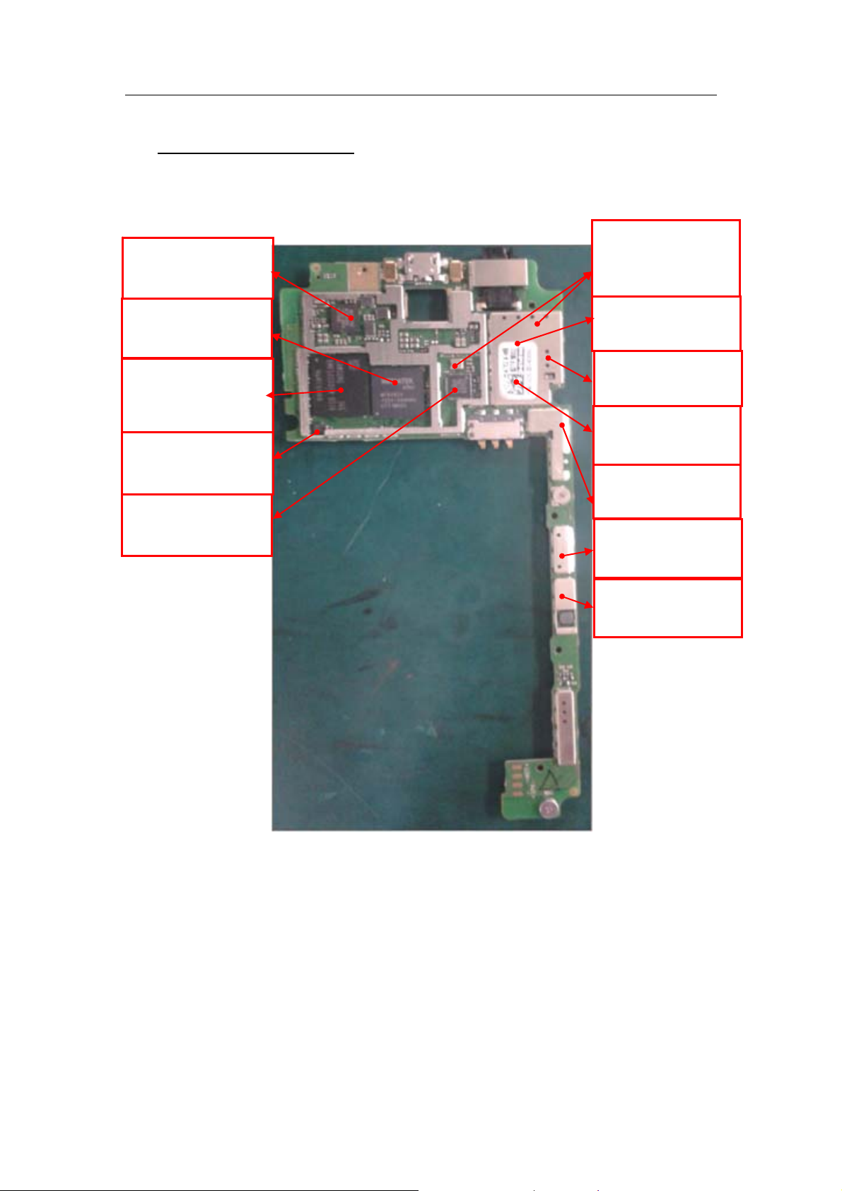
U501 Power Management
Damage caused by failure:
large currents;does not boot;
X1101 X101 26M Crystals
Damage caused by failure::
Can not boot;WIFI、GPS、BT、
FM test fail
U108 BBIC
Damage caused by failure
does not boo;crashes
U401 NAND SDRAM
Damage caused by failure:
does not boot; showing white;
storage failures,;software
problems
U801 G-sensor IC
Damage caused by failure: The
screen can not be rotated
U1102 MT6627 IC
Damage caused by failure:
WIFI/GPS/FM/BT does not
work
U106 RF-TR
Damage caused by failure:
RF faults,Call fault
U204/U205 RX filter
Damage caused by failure:
Call failed
U101 RF PA
Damage caused by failure::
Call fault
U502 Charger IC
Damage caused by failure:
Does not charge:
U303Audio PA IC
Damage caused by failure::
Call fault
U701 Backlight driving chip
Damage caused by failure:
NO display
5
LENOVO
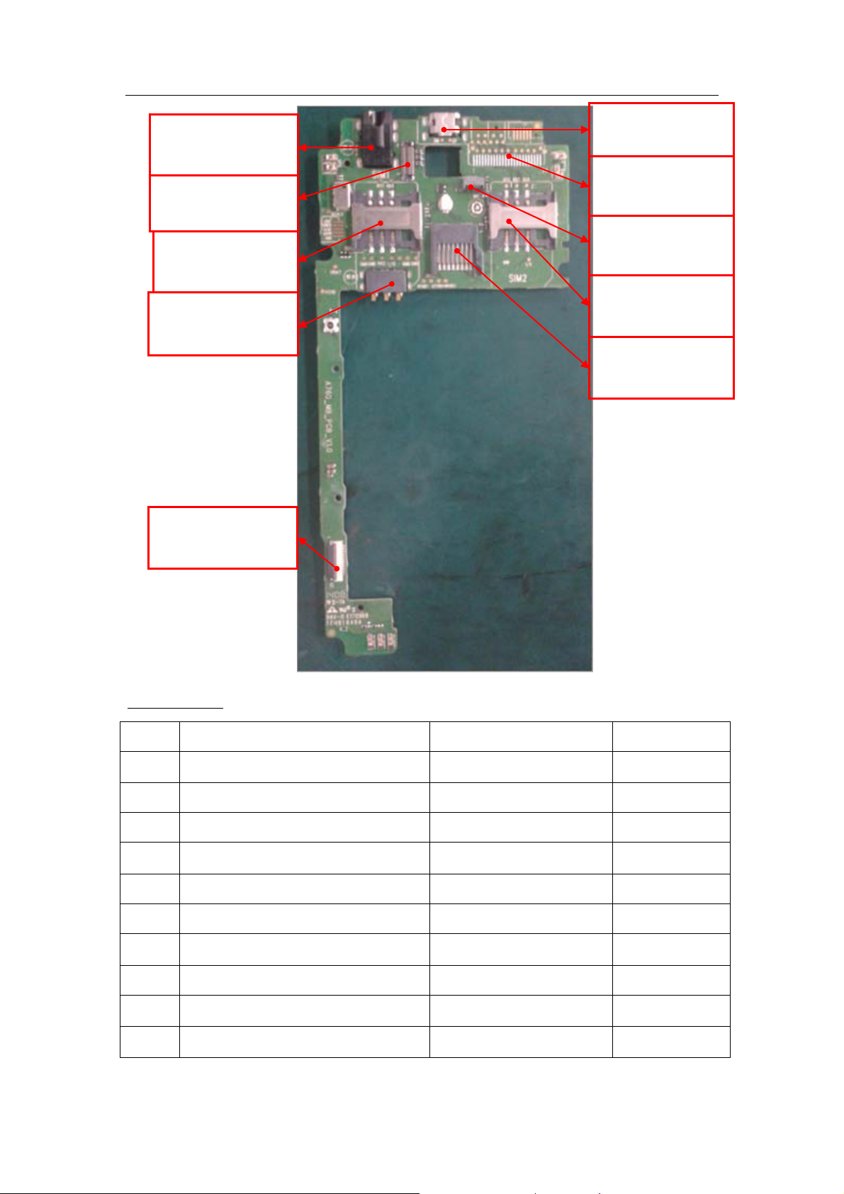
J801 Headphone Jack
Damage caused by failure:
Headphones silent;
not receive FM
J601 Back camera
Damage caused by failure:
Camera does not work
J601 SIM card
Damage caused by failure:
does not know the SIM card
J501 duo electrical
connector
Damage caused by failure:
does not boot; power down;
J901 LCD connector
Damage caused by failure:
Does not display
J802 USB Connector
Damage caused by failure:
Doesn’t charge,data transmit
J1003 Front camera
Damage caused by failure:
Cannot take photo
J902 CTP connector
Damage caused by failure:
No Touch
J602 SIM card
Damage caused by failure:
does not know the SIM card
J603 T-flash card
Damage caused by failure:
does not know the T-flash
card;
Part name
ITEM Part No. Model QULITY
1 HQ11100239000 MT6582V/X 1
2 HQ11100133000 MT6166V 1
3 HQ11100242000 MT6323GA 1
4 HQ11110079000 MT6627N 1
5 HQ11120212000 5M39A46-5Z0//5M39A465Z0 1
6 HQ11160096000 VC5341 1
7 HQ11160115000 VC5348 1
8 HQ11150045000 ET5120A 1
9 HQ11220005000 WPT2N41-8/TR 1
10 HQ11180029000 BMA223 1
6
LENOVO
1-2. Product Main Function
¾ Support Camera
¾ Music player
¾ Support T-Flash card
¾ Support WIFI
¾ 4.0" WVGA LCD
¾ Support
GSM850&GSM900&DCS1800&PCS1900&WCDMA900&WCDMA210
0 Network
¾ Support Bluetooth
¾ Support FM radio
¾ Support dual SIM card
¾ Support G-sensor
¾ Support GPS
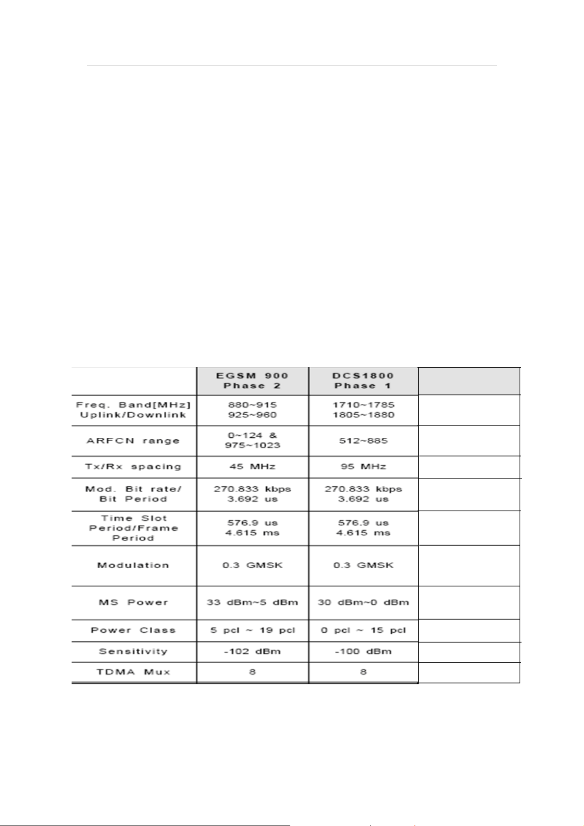
1-3. General Specificatio
PCS1900
1850~1910
1930~1990
512~810
80 MHz
270.833 kbps
3.692 us
576.9 us
4.615 ms
0.3 GMSK
30 dbm~0 dbm
0 pcl~15 pcl
-100 dbm
8
7
LENOVO
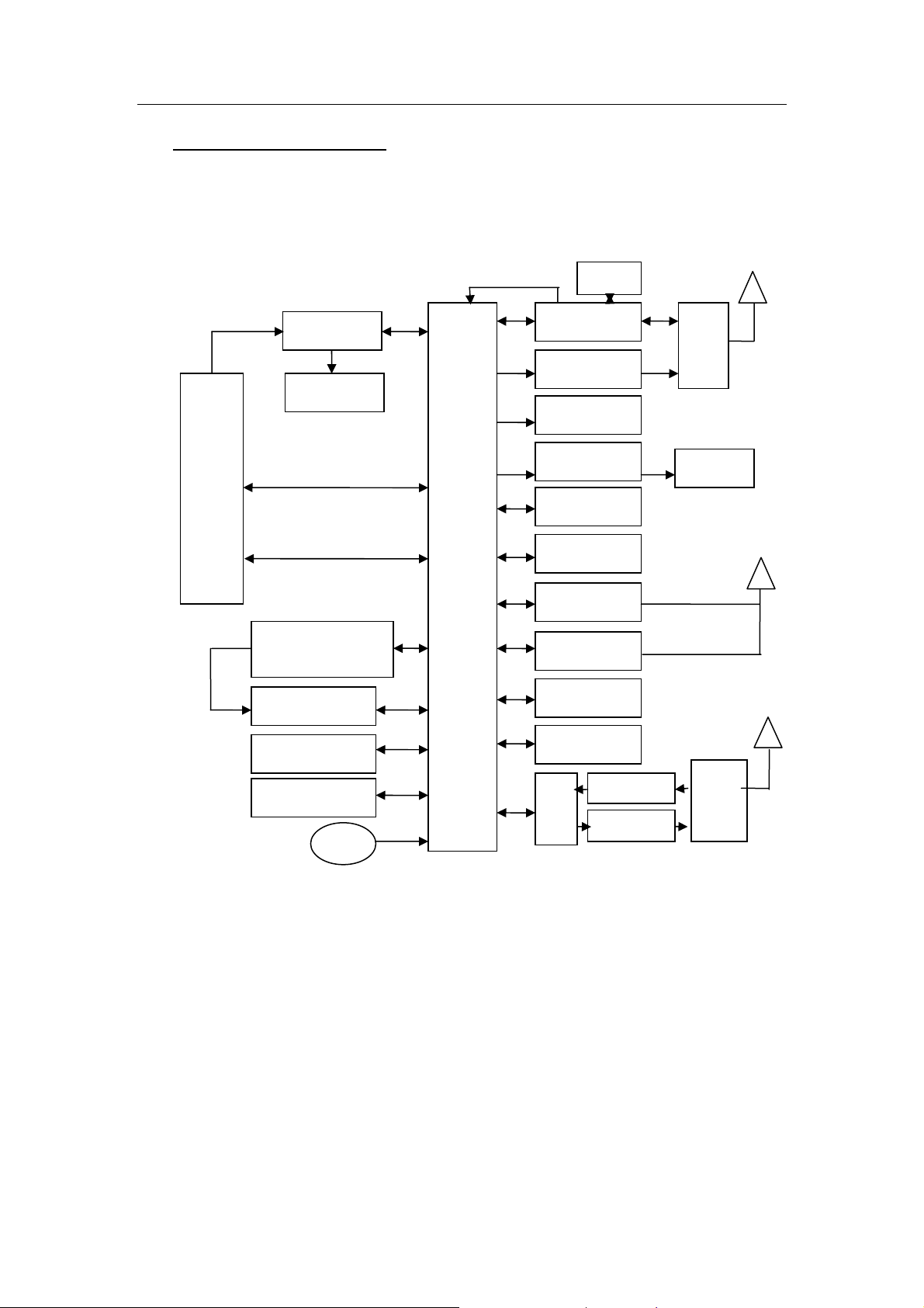
2. Block Diagrams
2-1. System Diagrams
5V IN
USB DM/DP
URAT TX/RX
ANT
Remark:FM/GPS/WIFI/BT to Four in Chip;
5PIN USB
Charger
Battery
MT6582(U108)
3.5MM
Earphoen
FM Radio
Side Health
WVGA LCD
MIC
26M
RF-TR
RF-PA
SIM 1/SIM
Audio_PA
T-FLASH
Camera
Bluetoot
WIFI IC
Receiver
ROM+RAM
TX PA
Speak
RF Swit
2-1-1 BBIC Diagrams
MediaTek MT6572 is based on four core ARM architecture (28nm A7
architecture) ,frequency of 1.3 GHz,can be seen MT6572 quad-core upgraded
or modified MT6589 , in addition the GPU or the first TD-SCDMA and WCDMA
dual-mode integrated in the same single chip(can be seen as MTK6582 will
bring TD baseband chips ,the disputed).At the same time ,mediatek will also
launch MT6582M Mt6582 cheap version . Including mediatek MT6582
highest level support 720P resolution screen ; Mediatek Mt6582 is the highest
level can only support the QHD screen .Frequency is 1.3GHz,collocation of
8
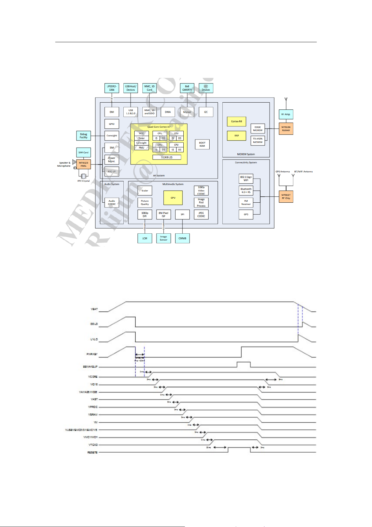
LENOVO
GPU models for SGX still 544.
Typical application diagram is shown in nether figure
Application Diagram of MT6582
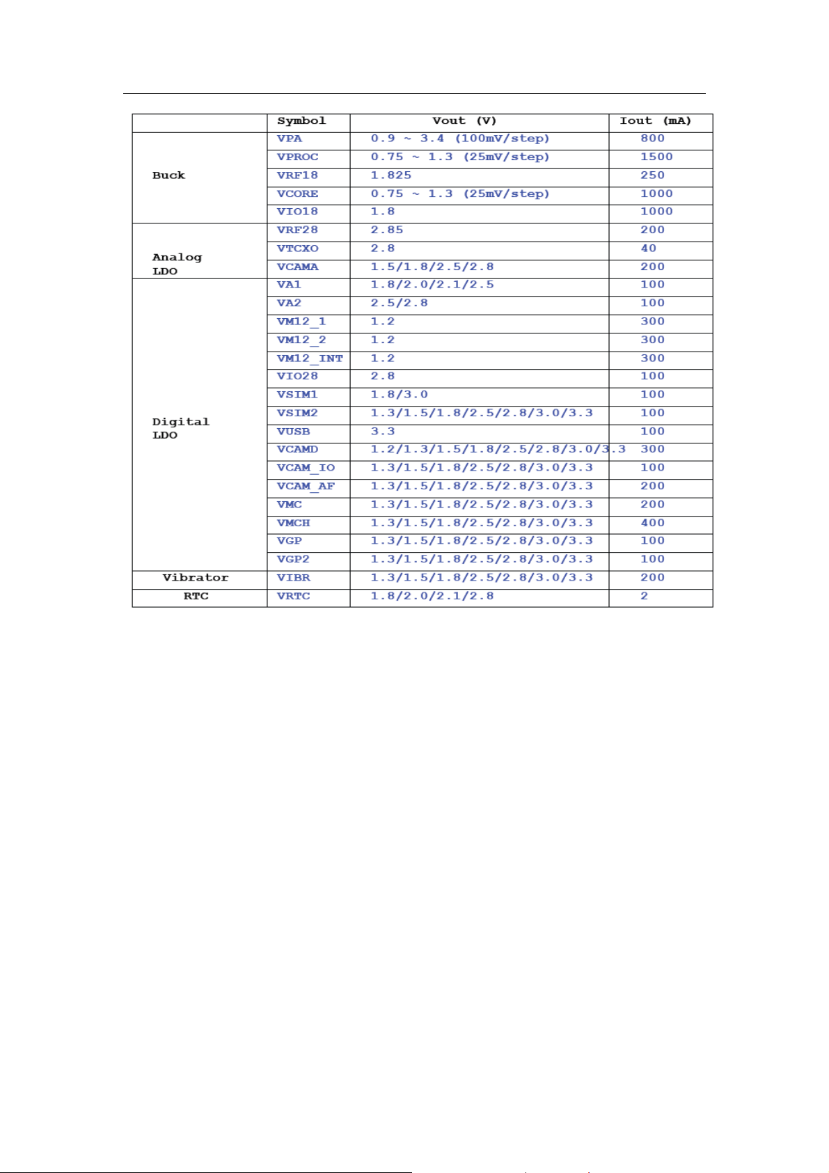
2-2. Power Management Diagrams
9
LENOVO
10
LENOVO
3. Flow Chart of Troubleshooting
3-1.Baseband
3-1-1. Phone does not start up troubleshooting
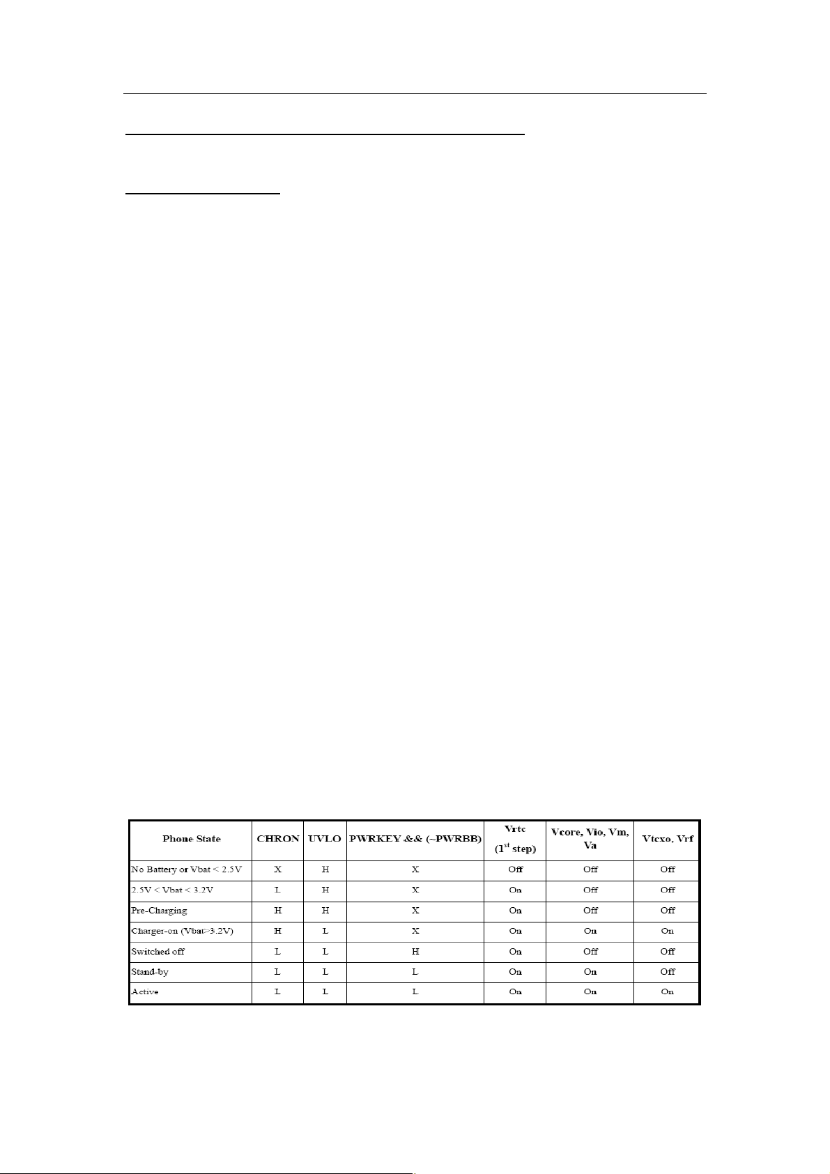
Power-on Sequence and Protection Logic:
The PMU handles the powering ON and OFF of the handset. There are three
ways to power-on the handset system :
① Push PWRKEY (Pull the PWRKEY pin to the low level)
② RTC module generate PWRBB to wakeup the system
③ Valid charger plug-in (CHRIN voltage is within the valid range)
Pulling PWRKEY low is the typical way to turn on the handset. The Vcore
buck converter will be turned-on first, and then Va/Vio/Vm LDOs turn-on at
the same time. After that, the supplies for the baseband are ready and it will
send the PWRBB signal back to PMU for acknowledgement. To successfully
power-on the handset, PWRKEY should be kept low until PMU receives the
PWRBB from BB. Besides, the system reset ends at the moment when the
Vcore/Va/Vio/Vm are fully turned-on to ensure the correct timing and function.
If the RTC module is scheduled to wakeup the handset at some time, the
PWRBB signal will directly control the PMU. In this case, PWRBB becomes
high at the specific moment and let PMU power-on just like the on-sequence
described above. This is the case named RTC alarm.
Charger plugging-in will also turn on the handset if the charger is a valid
charger. However, if the battery voltage is too low to power-on the handset
(UVLO state), the system won’t be turned-on by any of the three ways. In this
case, charger will charge the battery first and the handset will be
powered-on automatically as long as the battery voltage is high enough.
States of mobile handset and regulator
11
LENOVO
Troubleshooting flow chart
Main related component: BBIC(U108),NAND+SDRAM(U401), XTAL
CRYSTAL(X101),RF-TR(U201), PMIC(U501),Power button.
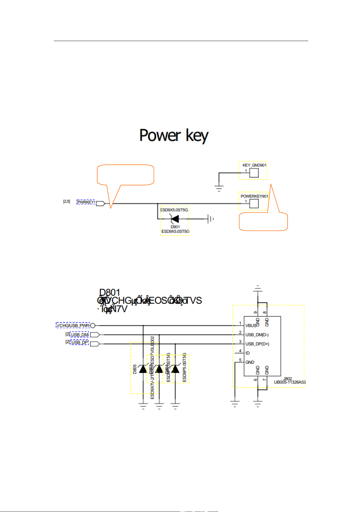
Power ON/OFF and download circuit
From BBIC
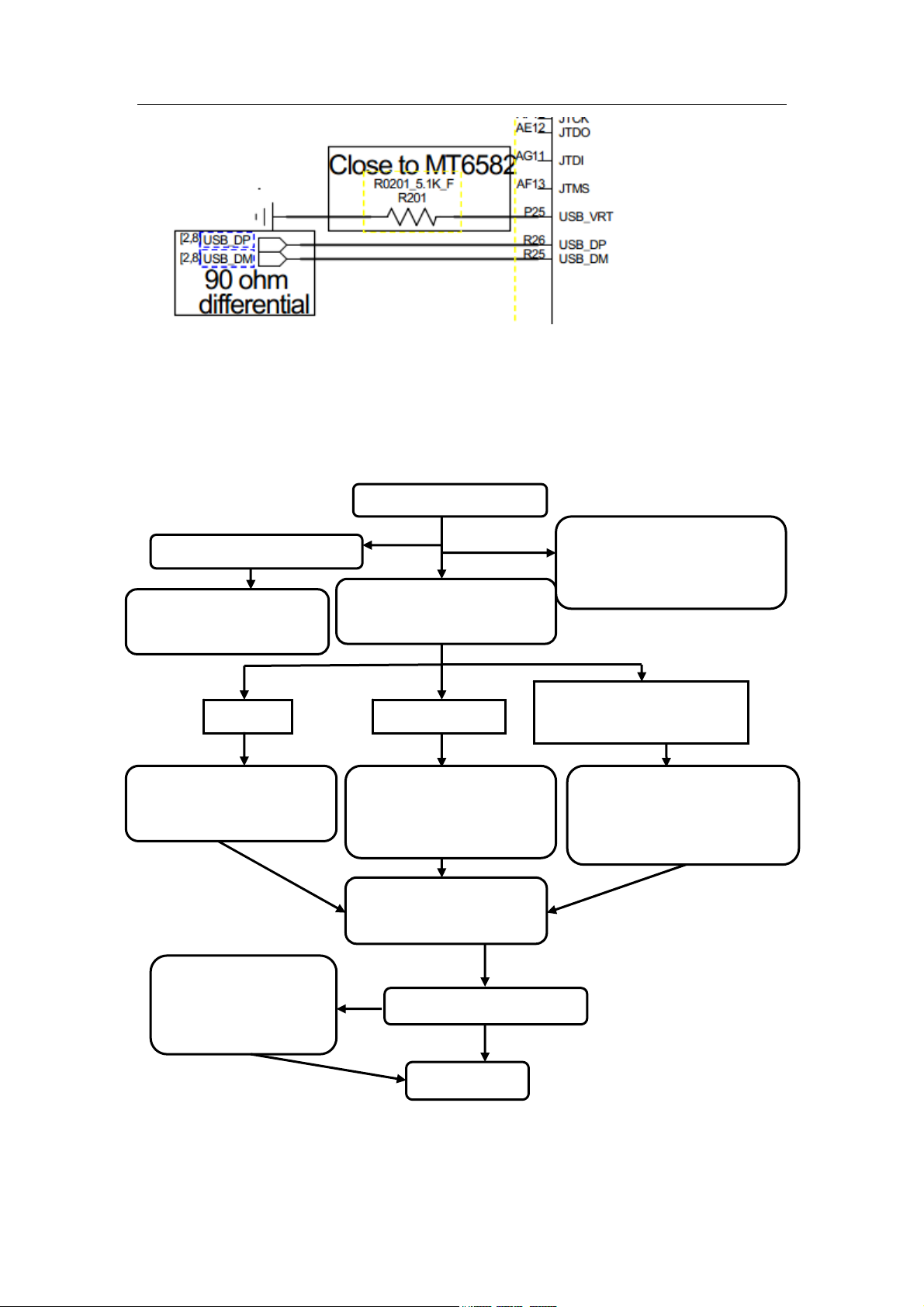
POWER KEY
¾ MINI USB CIRCUIT
12
LENOVO
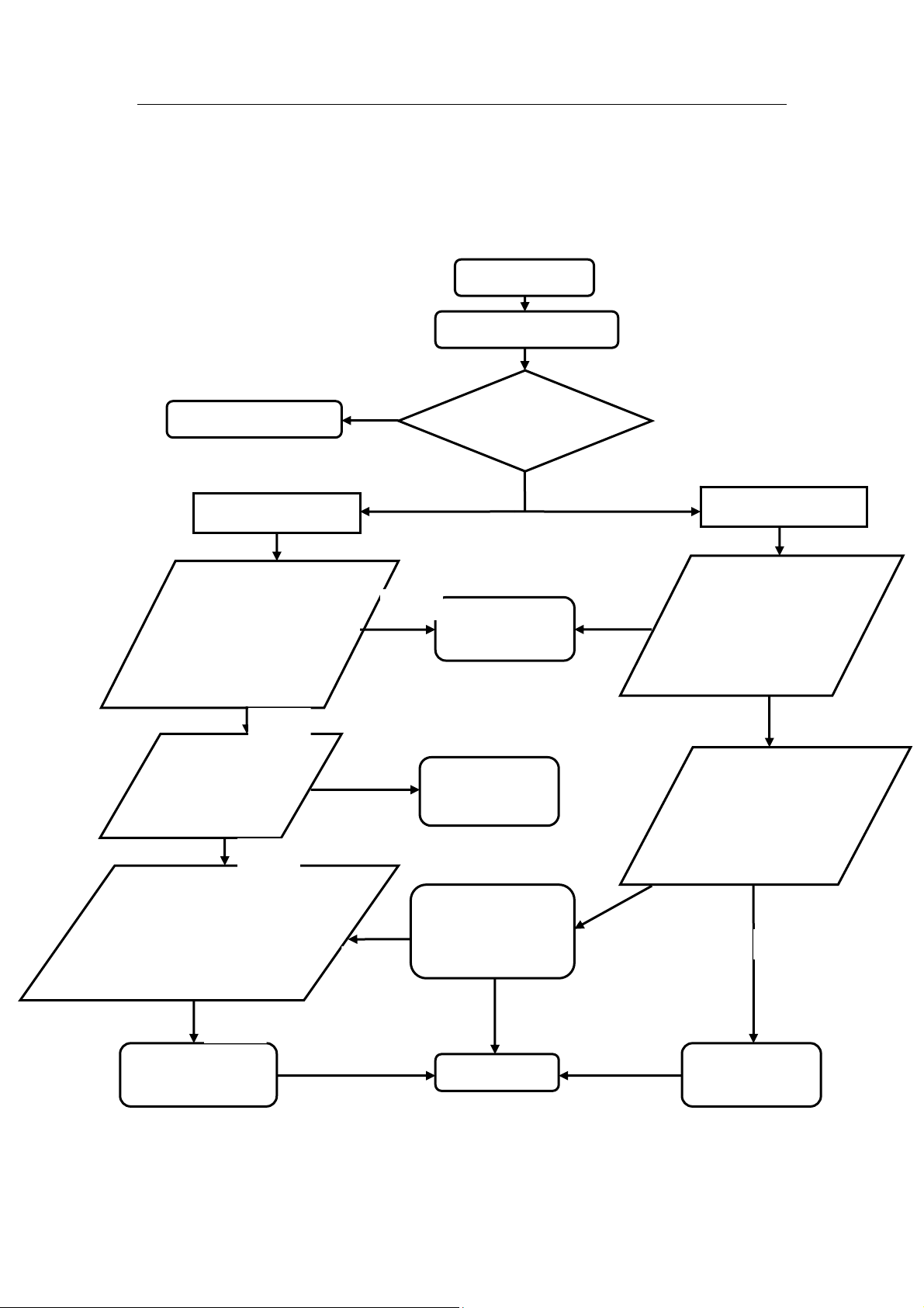
Download troubleshooting
Main related component: BBIC(U108),NAND+SDRAM(U401),RF-TR(U106),
XTAL CRYSTAL(X101), MINI USB(J802).
UART connection fault
Soldered again or replace
BBIC
≤20MA ≥30-200MA
Check the clock generation
circuit(related to BBIC)
Check the BB path
component in place and
of correct value type
Download fault
Press phones power key
Observe the current
Check the baseband
circuit(related to BBIC
Keypad FPC,LCD )
Soldered again or replace
damaged component
Download software again
END
Check circuit component
visually .soldered again or
replace damaged component
Current is large
(about 1 A or higher)
Check the Vbat circuit
component(related to
BBIC .PMIC.TR.PA.LCD....)
13
LENOVO
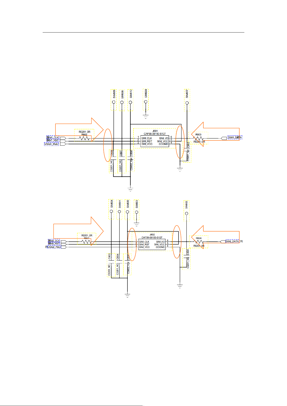
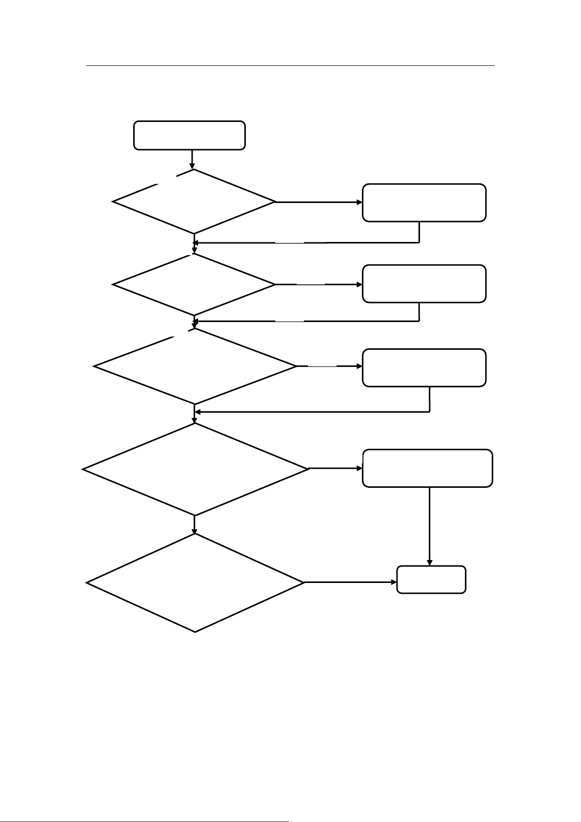
3-1-2. SIM troubleshooting
Troubleshooting flow chart
Main related component: BBIC(U108), SIM connector(J601,J602)
Select correct mode
SIM1&SIM2 all fault
Check SIM connector
solder joint and spring
contacts,Are these OK?
YES
SIM fault
Clean SIM connector
NO
Check SIM work
mode correct OK?
YES
NO NO
Soldered again or
replace
SIM1&SIM2 all fault
Check SIM connector
solder joint and spring
contacts,Are these OK?
YES
Measure SIM working
Voltage Normal 2.8V
YES
Check the path component
Are the component in place and of
correct value/type.
YES
Check BBIC soldered
again or replace
NO
NO
Check BBIC soldered
again or replace
Replace
damaged/missing
component
END
Check the path component
Are the component in place
and of correct value/type.
NO
YES
Check BBIC soldered
again or replace
14
LENOVO
SIM CIRCUIT
¾ SIM1&SIM2
From BBIC
From BBIC
From BBIC
From BBIC
3-1-3. MIC troubleshooting
Troubleshooting flow chart
Main related component: BBIC(U108),MIC
15
LENOVO
g
g
p
p
Microphone does not work
YES
Check MIC circuit
component visually
YES
NO
NO
Soldered again or replace
ed component OK?
dama
NO
NO
Soldered again or replace
ed component OK?
dama
Check microphone
OK?
YES
Is the bias Voltage 2.4V
measured from MICP
YES
NO
NO
Check BBIC Soldered again or
re
Check the MIC path component
Are the component in place
and of correct value/type
YES
Replace damaged/missing
com
YES
Check PMIC 、 KB board
connector soldered again or
replace
lace
onent
END
16
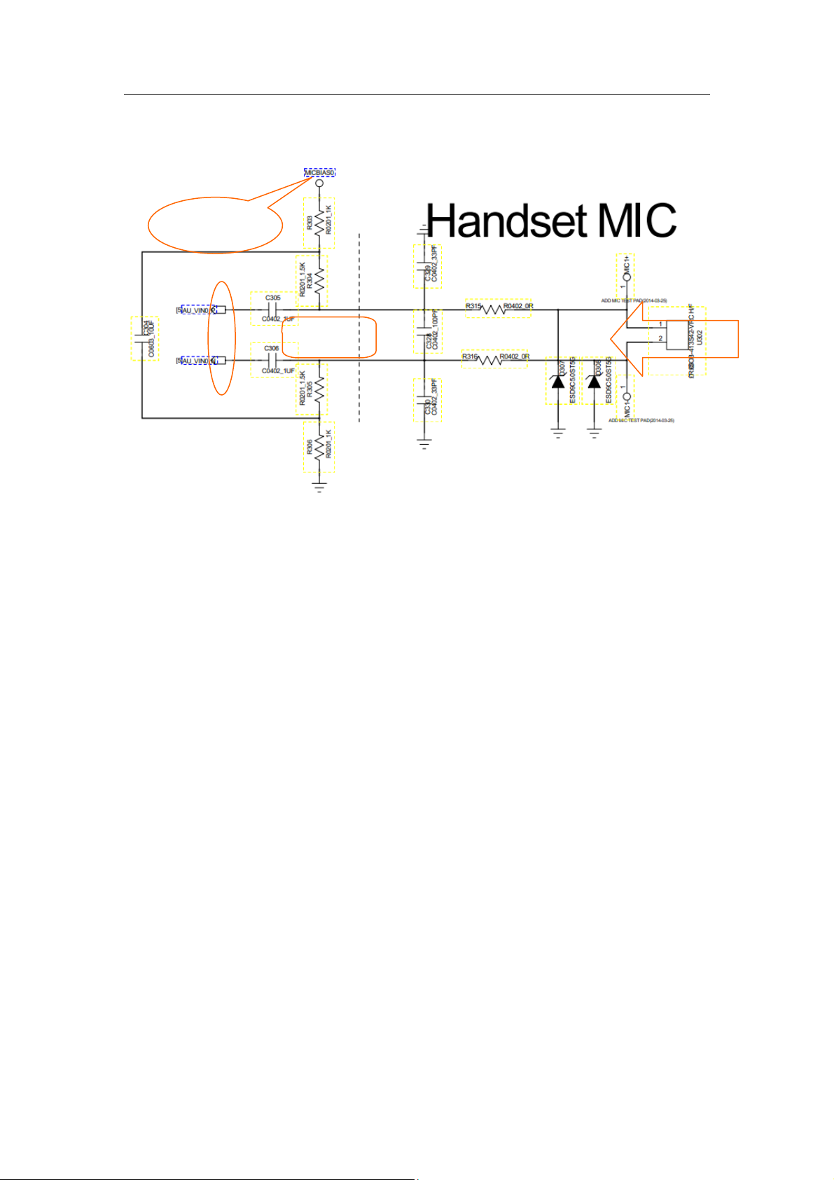
LENOVO
MIC circuit
FromPMIC
To BBIC
From MIC
17
LENOVO
p
3-1-4. T-Flash troubleshooting
Troubleshooting flow chart
Main related component: BBIC(U108),T-FLASH CONNECTOR(J603).
Phone does not read T-Flash
Check T-Flash card
OK?
YES
Replace T-Flash
NO
Check T-flash connector
solder joints and spring
contacts is OK
NO
Solder again or replace
IS T-Flash working NOW
YES
NO
Measure T-Flash card work
voltage(VDD)=2.8V
NO
Check BBIC Soldered
again or replace
YES
Measure CLK.CMD.CSN&DAT
correct signal is OK?
NO
YES
Check BBIC Soldered
again or replace
YES
Check T-Flash card path
component in place and of
correct value/type
YES
Replace damaged/missing
com
onent
Check BBIC soldered again or
replace
END
18
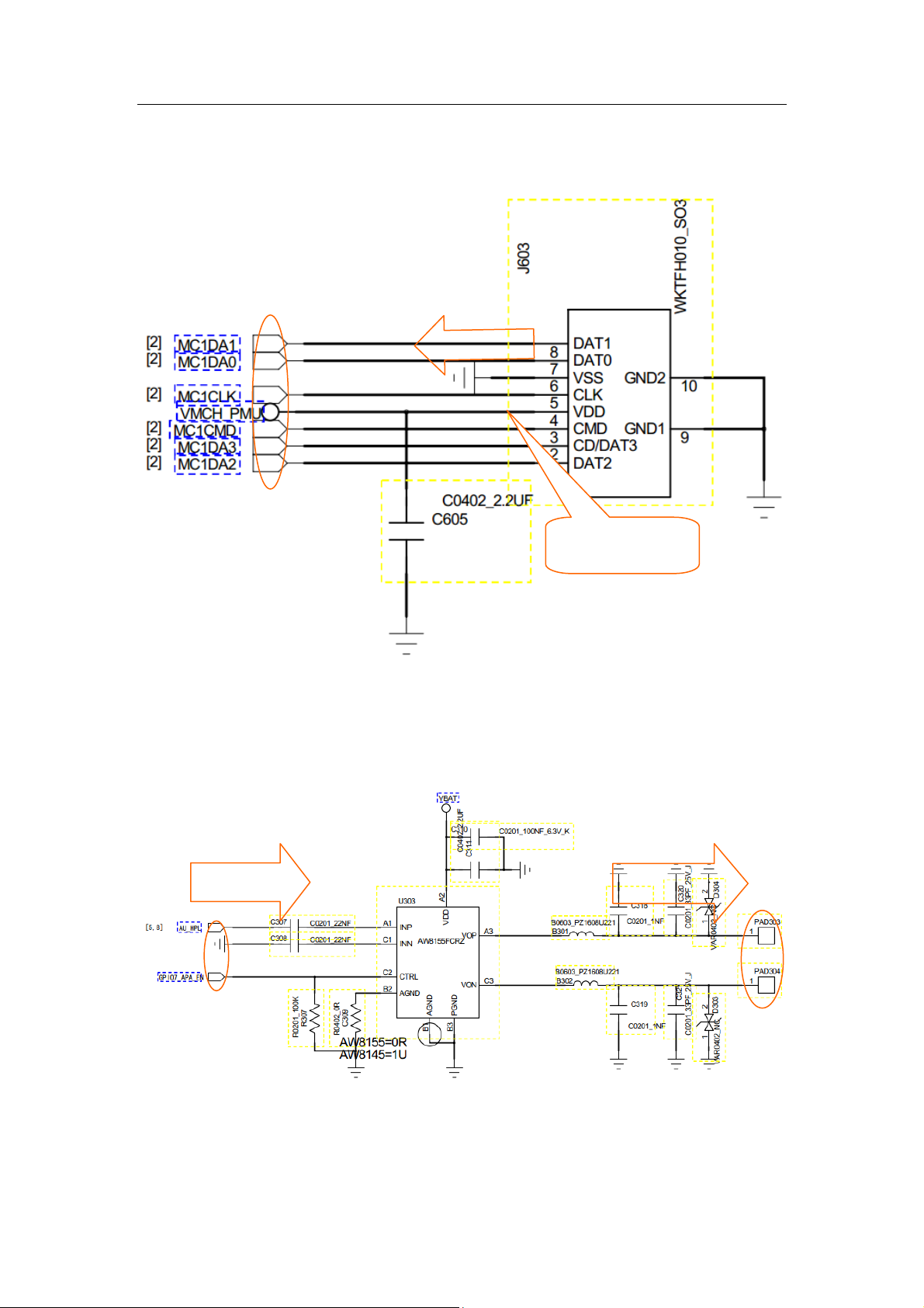
LENOVO
T-Flash circuit
To BBIC
3-1-5. Speaker troubleshooting
Speaker circuit
From BBIC
Voltage From U502
To speaker
Troubleshooting flow chart
Main related component: BBIC(U108),SPEAKER
19
LENOVO
p
Speaker does not work
Check Speaker
YES
OK?
Replace Speaker
NO
Check Audio circuit
component visually
NO
Solder again or replace
The damaged component OK?
YES
Measure Audio PA work
voltage(VBAT)
Normal:3.6-4.2V
NO
NO
Check PA VBAT circuit
YES
Measure Audio PA enable
signal(AUDIO-EN)Normal:2.8V
NO
Check BBIC Soldered
again or replace
YES
Check the speaker path
component,Are the components in
place and of correct value/type
NO
Replace damaged/missing
Check the BBIC and Audio-PA
soldered again or replace
YES
com
YES
onent
END
20
LENOVO
g
p
p
p
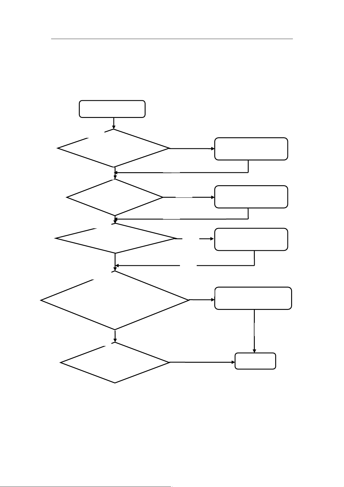
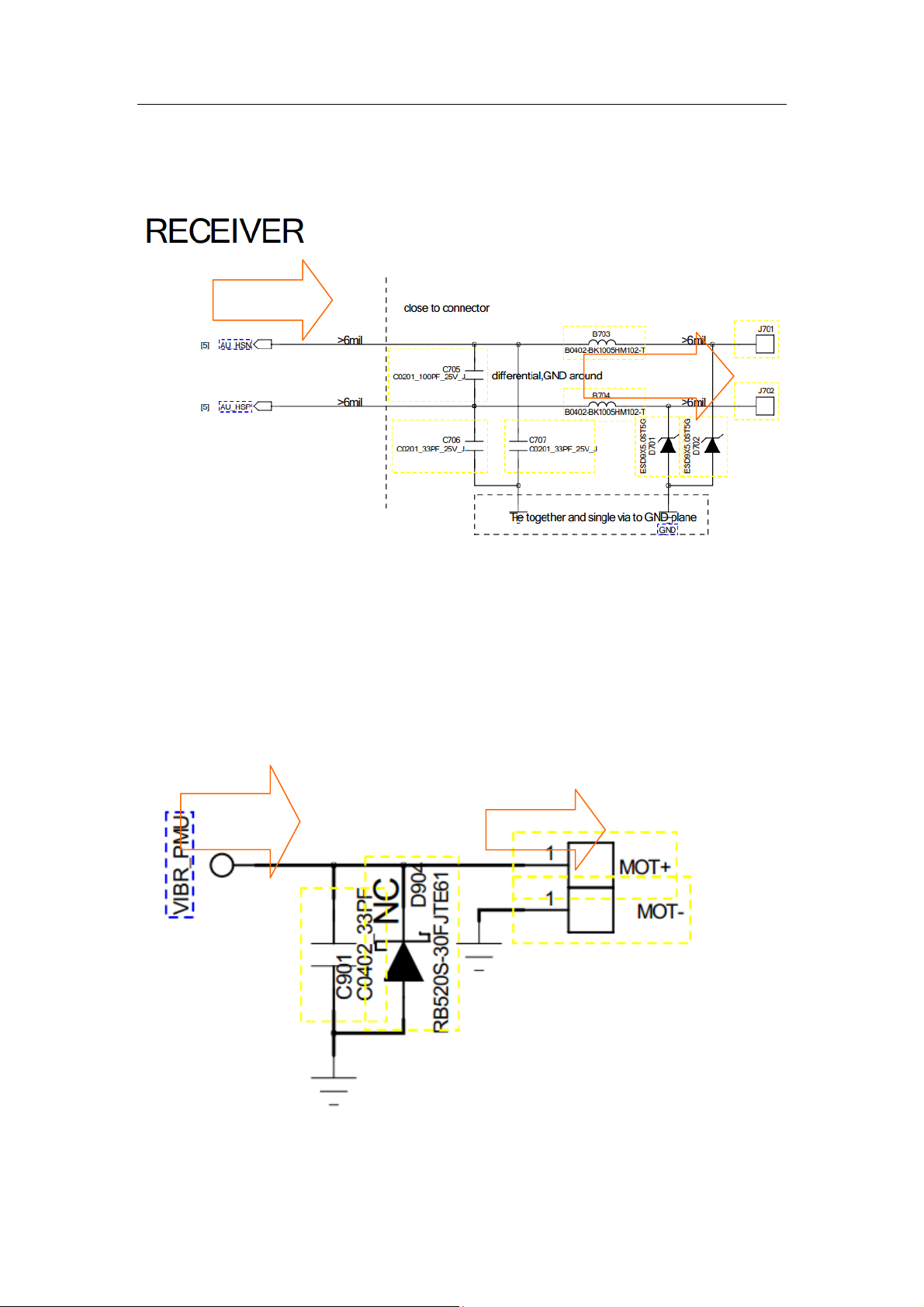
3-1-6. Receiver troubleshooting
Troubleshooting flow chart
Main related component: BBIC(U108),Receiver
Earpiece does not work
YES
Check Earpiece circuit
component visually
YES
NO
NO
Soldered again or replace
ed component OK?
dama
NO
NO
Soldered again or replace
iece working now?
IS ear
Check earpiece
OK?
YES
Check earpiece PAD
NO
Check BBIC Soldered again or
lace
re
YES
NO
Check the earpiece path
component Are the component in
place and of correct value/type
NO
Replace damaged/missing
onent
com
YES
YES
Check BBIC soldered
again or replace
YES
END
21
LENOVO
Receiver circuit
From BBIC
To receiver
3-1-7. Vibra troubleshooting
Troubleshooting flow chart
Main related component: BBIC,MOTOR,KB board ConnectorJ1201
Vibra circuit
From PMIC
To VIB
22
 Loading...