

Page 1

Appendix C
LW400-09A Digital Output Option
Introduction The LW400-09A Digital Output option provides 8-bit TTL and
ECL, digital outputs corresponding to the current value of the
channel 1 analog output. The latched digital data, which is held
for the duration of the sample clock, is available via two rear
panel mounted connectors. Digital data is available whenever
the channel 1 output is enabled.
LW400’s, with the digital output option, include a special digital
editing mode for the creation of user specified data patterns.
Byte wide data patterns or selected bits within the 8-bit wide
digital word may be programmed. Digital data patterns created
using this editor are identified as “Digital” waveforms. Digital
waveforms can be edited using the same “cut and paste” tools
available for analog waveforms. The major difference between
the two waveform types is that digital waveforms are not
processed to remove discontinuities at transitions. This also
means that Time editing functions, such as sub-sample Move,
are not useable with digital waveforms and are limited to analog
waveforms only.
Specifications
Digital outputs:
Digital output modes: ECL, TTL all available on output connectors simultaneously.
Mating output connector: SMB for ECL output
Maximum data
output clock rate: ECL, 400 MBytes/sec; TTL 100 MBytes/sec.
8 bits corresponding to the channel 1 analog output plus CLOCK
and CLOCK* (TTL only).
20 pin P/N 3M-3421-7020 for TTL output.
C-1
Page 2
Appendix C
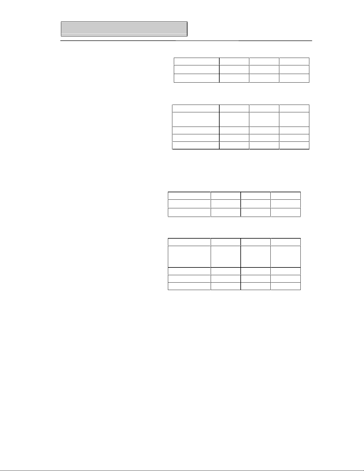
ECL outputs: Levels:
Parameter Min Typ Max
Note: output load is 50 Ω to -2 Volts.
Timing:
Parameter Min Typ Max
Clock to
Analog Output
Setup Time * T-660 ps T-485 ps T-310 ps
Hold Time 310 ps 485 ps 660 ps
Data skew - 80 ps 250 ps
* T is clock period (i.e. 2.5 ns for 400 MHz clock)
TTL :
Levels:
Parameter Min Typ Max
V
V
V
OH
OL
OH
V
OL
-0.98 V -0.8 V -0.71V
-1.95 V -1.8 V -1.58 V
7 ns 8 ns 9.8 ns
2.00 V 2.60 V -
- 0.35 V 0.80 V
Timing:
Parameter Min Typ Max
Clock to
10 ns Analog
Output
Setup Time * T -5.7 ns T -0.5 ns T+3.9 ns
Hold Time -3.9 ns 0.5 ns 5.7 ns
Data skew - - 1 ns
* T is clock period (i.e. 10 ns for 100 MHz clock)
C-2
Page 3

CONNECTOR PINOUTS
Appendix C
Note1:
Note2: TTL outputs back terminated in 75 ohms
TTL Port 1 - TCLK 2 Ground
ECL Port J800 - D0 (LSB)
D7 signifies the bit which corresponds to analog signal most
significant bit (MSB), and D0 signifies the bit which corresponds
to the least significant bit (LSB).
3 - TCLK* 4 Ground
5 - D0 (LSB) 6 Ground
7 - D1 8 Ground
9 - D2 10 Ground
11 - D3 12 Ground
13 - D4 14 Ground
15 - D5 16 Ground
17 - D6 18 Ground
19 - D7 (MSB) 20 Ground
J700 - D1
J600 - D2
J500 D3
J400 - D4
J300 - D5
J200 - D6
J100 - D7 (MSB)
J900 - ECLOCK
C-3
Page 4

Appendix C
Interconnection Information:
TTL:
ECL: The LW400-09A provides 464 Ω internal pulldown resistors at
Cable Selection: For TTL output: Spectra Strip 843-132 - 280-020.
The LW400-09A includes 75 Ω back terminations on all the TTL
output lines. These resistors are used to match the transmission
line impedance taking into account the additional source
impedance of the TTL driver. The 75 Ω resistors match the 80
impedance of the flat cable fairly well. In this fashion, no
termination resistor is required or desired. The most important
consideration in this scheme is that the load should be as close
to an open circuit as possible. One, or at most, two TTL loads
should be placed at the termination of the line. Capacitance at
the termination will have a detrimental effect on the rise time of
the received signal. Every effort should be made to limit parasitic
capacitance at the termination of the cable to under 10 pF. All
grounds should be tied together at the load side of the cable.
the ECL output drivers. The ECL outputs need to be terminated
at the load side of the cable. The most optimum interconnection
would utilize ECL line receivers at the receiver end of the cable,
with termination resistors of 50 Ω tied to -2 Volts.
Ω
C-4
Page 5

Appendix C
C-5
Page 6

Appendix C
Creating A Digital Waveform A new digital waveform, as in the case of a new analog
waveform, is created by pressing the Select Wave button on the
front panel and choosing the New menu item. Select New CH1
Wave from the New menu and then enter the waveform name
in the Waveform menu field. Press the Accept softkey to
create the new waveform.
Figure C3.1
Press the EDIT button on the front panel of the WaveStation to
display the Edit menu. The presence of the LW400-09A Digital
Output option is indicated by the Digital Edit softkey shown in
Figure C3.1 above. Select Digital Edit to display the Digital
Edit menu, shown in figure C3.2 below.
Note that waveforms
created in this editor are tagged as “digital”. Digital waveforms
are not subject to signal processing functions to remove
discontinuities. They are also allowed to us e a wider range of
sample clock rates.
C-6
Page 7

Appendix C
Figure C3.2
Digital waveforms are created and edited by specifying the digital
value of the waveform, in hexadec imal, in the
value is entered, starting at the location specified in the Left
Cursor field, with a length set in the Duration field whenever the
Set Value softkey is pressed. The Duration and Left Cursor
fields will read out in units of tim e or sam ple points as selected
by the user using the Format softk ey switch. A user message,
”Use the m-M keys for entering A-F” appears on the display
while the Digital Edit or Bit Edit menus are displayed.
Note that the units multiplier buttons, m, µ, n, p, k, and M in the
numeric keypad, are redefined during digital editing as
hexadecimal characters A-F, respectively.
Value field. This
The Editor Options menu is used to select one of two editing
modes—Insert (Ins) or Overwrite (Ovr). In insert mode the new
digital waveform is inserted, starting at the left cursor location
while any existing waveform elements are displaced to the right
(later in time) by the duration of the new waveform. In overwrite
mode the enabled bits of the new digital waveform replace the
corresponding bits in any existing waveform, starting at the left
cursor location for the preset duration. The Bit Edit menu is
used to edit selected bits specified using a bit mask in
conjunction with the Value field—see figure C3.4 on page C-9.
C-7
Page 8

Appendix C
Digital waveforms are displayed on the LW400 as “Bus Level”
diagrams which show the time interval of each part of the
waveform having a given digital value. Individual bit waveforms
are not displayed. Digital waveform amplitude values can be
read, as hexadecimal numbers, from the time cursor amplitude
annotation fields, in the lower left corner of the LW400 display.
Note that the Volt Cursors must be turned off by pressing the
VOLT CURSOR button on the front panel and then selecting
Volt Cursors off as indicated by the displayed menu.
C3.2 above and the following figure C3.3 which shows an
example of the relationship between the cursor readout fields
and the actual bit patterns.
See figure
C-8
Page 9

Appendix C
Editing A Digital Waveform The Bit Edit menu is used to edit selected bits within a digital
word. The 8 bit wide Field Mask is used to enable the desired
bits. Setting a Field Mask bit to one (1), enables the
corresponding bit in the digital waveform. The actual value of
the enabled bit is determined by the user entered Masked
Value. A zero (0) in the field mask means that the
corresponding bit will be unchanged. Logically, the complement
of the field mask is AND’d with the existing data value and the
result is OR’d with the expanded version of the masked value.
Symbolically, this is expressed as:
Edited Value = (Value
• Field Mask) + (Masked Value)
existing
The most significant bit (MSB) of the field mask, corresponding
to the MSB in the digital waveform(D7) is shown on the left.
Similarly, the least significant bit (LSB), corresponding the LSB
(D0) of the digital waveform is shown at the right.
Figure C3.4
C-9
Page 10

Appendix C
Consider the
field mask is set to 00001011 enabling 3 bits(D3, D1, and D0).
The Masked Value, entered as a hexadecimal number, is set to
5(101 in binary). The 3 enabled bits are set to this value, D3=1,
D1=0 and D0=1. The digital waveform Value is hexadecimal 41.
And the expanded mask value is 1.
Bit Edit menu values shown in figure C3.4 . The
Note that the Value is read
out at the left cursor position and displayed in the Left Cursor
menu field.
In the overwrite mode, only the enabled bits are replaced in an
existing waveform. This is a simple way to edit selected bits in
an existing digital waveform. For example, by setting the Field
Mask to 10000000, in overwrite mode, the MSB (D7) can be
edited starting at the left cursor location for the length set by the
duration field.
In Insert mode, since the existing data is displaced, the
expanded mask value is inserted into the waveform.
The following figure (figure C3.5) illustrates the relationship
between the Field Mask, Masked Value, Value, and the
resulting digital waveform bit pattern.
Figure C3.5
C-10
Page 11

Appendix C
Setting Clock Rates For
Digital Waveforms The clock rate associated with a digital waveform has a much
greater range of values than is available with analog waveforms.
The clock on the LW400 and the LW400A can be set, by
entering the frequency in the Clock Rate field on the CLOCK
CONTROL menu. The clock ranges are described below:
Lower Limit MHz Upper Limit MHz
355.000000 400.000000
177.500000 200.000000
118.333333 133.333333
88.750000 100.000000
71.000000 80.000000
59.166667 66.666667
50.714286 57.142857
0.006000 50.000000
In addition the LW400A has a continuous clock that can be
set over a range of 6 kHz to 400 MHz, with 1 Hz resolution.
Refer to section 13 for addtional information related to setting
the clock on the LW400 and LW400A.
C-11
Page 12

Appendix C
Importing Digital Waveforms Digital waveforms can be imported directly into AWG’s with the
LW400-09A Digital Output option. Any Easywave .WAV file as
well as ASCII Hex and ASCII Binary files can be imported as
digital waveforms.
Figure C3.6
The Easywave .WAV file contains a single channel waveform
created using LeCroy’s Easywave waveform creation software.
ASCII Hex files contain groups of 2 digit hexadecimal numbers
(0-F) separated by spaces. For example:
13 F0 03 8D C6 ...
ASCII BINARY files consist of groups of eight binary numbers
(0’s or 1’s) separated by spaces. For Example:
10101010 00001011 01101111 ...
Waveforms are imported by pressing the PROJECT button then
selecting the Import menu—see figure C3.6 above. Choose
Digital Esywv, ASCII HEX, or ASCII BINARY in the What field.
Select the desired Source File and press the Import soft key.
The selected file will be imported into the current project as a
digital waveform. Use the Select Wave button to select the
waveform for editing.
C-12
Page 13

Appendix C
Analog Output for
Digital Waveforms When a digital waveform is created the amplitude for the analog
output is limited to the range of ( 500 mV, with -500 mV
corresponding to the digital hex code 00 and +500 mV
corresponding to the digital hex code FF .
After a digital waveform is created, changing the amplitude or
offset affects the output amplifiers only and not the DAC. As a
result there will be no change to the digital codes when the
amplitude or offset is changed, however the analog output
amplitude and offset will change based on the modified settings.
If it is desirable to produce an analog output with other than the
(500 mV output the amplitude and offset need to be changed to
the desired settings each time the waveform is loaded.
If an analog waveform is inserted into a digital waveform care
must be taken to restrict its maximum voltage to ≤500 mV and
the minimum voltage ≥-500 mV, otherwise the output will be
incorrect.
Waveform Sequences Using
Digital Waveforms Digital waveforms can be combined in waveform sequences
using the sequence editor in the normal manner. There is one
key thing to keep in mind when creating sequences with digital
waveforms. The signal processing functions used in generating
sequences of analog waveforms are not used. Waveforms
cannot be resampled to correct errors in timing caused by using
segments created using different sampling rates. Therefore, if
digital waveform segments are created at different clock rates,
the highest clock rate is used when the sequence is compiled.
Essentially, digital sequences always preserve points and timing
errors can occur if you are not careful. To avoid timing errors
it is a good practice to create sequences from digital
waveform segments which use the same clock rate.
If you create a sequence using both analog and digital
waveforms, then the sequence will be compiled as an analog
waveform and the digital segments may be resampled, causing
errors. It is advisable not to mix analog and digital
segments within the same sequence.
C-13
 Loading...