

Page 1
LeCroy Waverunner2 Series
Service Manual
LTXXX2-SM-E
Version D- December 2003
Page 2

LeCroy Corporate Headquarters
700 Chestnut Ridge Road
Chestnut Ridge, NY 10977-6499
USA
Tel: (845) 425-2000
Fax: (845) 425-8967
http://www.lecroy.com
Copyright © October 2001. LeCroy is a registered trade-mark of LeCroy Corporation.
All rights reserved. Information in this publication supersedes all earlier versions.
Specifications subject to change.
Page 3

1. Warranty and Product Support
It is recommended that you thoroughly inspect the contents of the oscilloscope
packaging immediately upon receipt. Check all contents against the packing
list/invoice copy shipped with the instrument. Unless LeCroy is notified promptly of
any missing or damaged item, responsibility for its replacement cannot be accepted.
Contact your nearest LeCroy Customer Service Center or national distributor
immediately (see chapter 2 for contact numbers).
1.1 Warranty
LeCroy warrants its oscilloscope products for normal use and operation within
specifications for a period of three years from the date of shipment. Calibration each
year is recommended to ensure in-spec. performance. Spares, replacement parts and
repairs are warranted for 90 days. The instrument's firmware has been thoroughly
tested and is thought to be functional, but is supplied without warranty of any kind
covering detailed performance. Products not made by LeCroy are covered solely by
the warranty of the original equipment manufacturer.
Under the LeCroy warranty, LeCroy will repair or, at its option, replace any product
returned within the warranty period to a LeCroy authorized service center. However,
this will be done only if the product is determined after examination by LeCroy to be
defective due to workmanship or materials, and not to have been caused by misuse,
neglect or accident, or by abnormal conditions or operation.
Read this First
1.2 Product Assistance
Note: This warranty replaces all other warranties, expressed or implied, including but
not limited to any implied warranty of merchantability, fitness, or adequacy for any
particular purpose or use. LeCroy shall not be liable for any special, incidental, or
consequential damages, whether in contract or otherwise. The client will be responsible
for the transportation and insurance charges for the return of products to the service
facility. LeCroy will return all products under warranty with
Help on installation, calibration, and the use of LeCroy equipment is available from the
LeCroy Customer Service Center in your country.
1.3 Maintenance Agreements
LeCroy provides a variety of customer support services under Maintenance
Agreements. Such agreements give extended warranty and allow clients to budget
maintenance costs after the initial three-year warranty has expired. Other services
such as installation, training, enhancements and on-site repairs are available through
special supplemental support agreements.
1.4 Staying Up to Date
LeCroy is dedicated to offering state-of-the-art instruments, by continually refining
and improving the performance of LeCroy products. Because of the speed with which
physical modifications may be implemented, this manual and related documentation
may not agree in every detail with the products they describe. For example, there
might be small discrepancies in the values of components affecting pulse shape,
transport prepaid.
Read this First 1-1
Page 4

timing or offset, and — infrequently — minor logic changes. However, be assured the
scope itself is in full order and incorporates the most up-to-date circuitry. LeCroy
frequently updates firmware and software during servicing to improve scope
performance, free of charge during warranty. You will be kept informed of such
changes, through new or revised manuals and other publications.
Nevertheless, you should retain this, the original manual, for future reference
to your scope’s unchanged hardware specifications.
1.5 Service and Repair
Please return products requiring maintenance to the Customer Service Department in
your country or to an authorized service facility. The customer is responsible for
transportation charges to the factory, whereas all in-warranty products will be returned
to you with transportation prepaid. Outside the warranty period, you will need to
provide us with a purchase order number before we can repair your LeCroy product.
You will be billed for parts and labor related to the repair work, and for shipping.
1.6 How to return a Product
Contact the nearest LeCroy Service Center or office to find out where to return the
product. All returned products should be identified by model and serial number. You
should describe the defect or failure, and provide your name and contact number. In
the case of a product returned to the factory, a Return Authorization Number (RAN)
should be used.
Return shipments should be made prepaid. We cannot accept COD (Cash On
Delivery) or Collect Return shipments. We recommend air-freighting.
It is important that the RAN be clearly shown on the outside of the shipping package
for prompt redirection to the appropriate LeCroy department.
1.7 What Comes with Your Scope
The following items are shipped together with the standard configuration of this
oscilloscope:
• Front Scope Cover
• 10:1 10 MΩ PP006 Passive Probe — one per channel
• Two 6.3A 250 V Fuses, AC Power Cord and Plug
• Operator’s Manual , Remote Control Manual, Hands-On Guide
• Performance Certificate or Calibration Certificate, Declaration of Conformity
Note: Wherever possible, please use the original shipping carton. If a substitute
carton is used, it should be rigid and packed so that that the product is surrounded by
a minimum of four inches or 10 cm of shock-absorbent material.
1-2 Read this First
Page 5

2. General Information
2.1 Product Assistance
Help on installation, calibration, and the use of LeCroy equipment is available from your
local LeCroy office, or from LeCroy’s
• Customer Care Center, 700 Chestnut Ridge Road, Chestnut Ridge,
New York 10977–6499, U.S.A., tel. (845) 578–6020
• European Service Center,
Switzerland, tel. (41) 22/719 21 11.
• LeCroy Japan Corporation, Sasazuka Center Bldg – 6
Sasazuka, Shibuya-ku, Tokyo Japan 151-0073, tel. (81) 3 3376 9400
2.2 Installation for Safe and Efficient Operation
4, Rue Moïse Marcinhes, 1217 Meyrin 1, Geneva
th
floor, 1-6, 2-Chome,
Operating Environment
For safe operation of the instrument to its specifications, ensure that the operating
environment is maintained within the following parameters:
Temperature ............. 5 to 40 °C (41 to 104 °F) rated.
Humidity.................... Maximum relative humidity 80 % RH (non-condensing) for
temperatures up to 31 °C decreasing linearly to 50 % relative
humidity at 40 °C
Altitude...................... < 2000 m (6560 ft)
The oscilloscope has been qualified to the following EN61010-1 category:
Installation (Overvoltage) Category ........................ II
Protection Class..........................… ........................ I
Pollution Degree ......................... ............................ 2
General Information 2-1
Page 6

Safety Symbols
Where the following symbols or indications appear on the instrument’s front or rear
panels, or elsewhere in this manual, they alert the user to an aspect of safety.
........................... CAUTION: Refer to accompanying documents (for Safety-
........................... CAUTION: Risk of electric shock
............................ On (Supply)
related information). See elsewhere in this manual wherever
the symbol is present.
[.................................... Standby (Supply)
............................ Earth (Ground) Terminal
...................... Alternating Current Only
........................ Chassis Terminal
............................ Earth (Ground) Terminal on BNC Connectors
WARNING................. Denotes a hazard. If a WARNING is indicated on the
instrument do not proceed until its conditions are
understood and met.
WARNING
Any use of this instrument in a manner not specified by the manufacturer
may impair the instrument’s safety protection.
2-2 General Information
Page 7

The oscilloscope has not been designed to make direct measurements on the
human body. Users who connect a LeCroy oscilloscope directly to a person do so at
their own risk. Use only indoors.
Power Requirements
The oscilloscope operates from 90–132 V AC 45-440 Hz, and 180–250 V AC; 45–66
Hz. No voltage selection is required, since the instrument automatically adapts to
the line voltage present.
Fuses
The power supply of the oscilloscope is protected against short-circuit and overload
by means of two 6.3 A/250 V AC
Disconnect the power cord before inspecting or replacing a fuse. Open the fuse box
by inserting a small screwdriver under the plastic cover and prying it open. For
continued fire protection at all line voltages, replace only with fuses of the specified
type and rating (see above).
“T”-rated fuses, located above the mains plug.
Ground
The oscilloscope has been designed to operate from a single-phase power source,
with one of the current-carrying conductors (neutral conductor) at ground (earth)
potential. Maintain the ground line to avoid an electric shock.
None of the current-carrying conductors may exceed 250 V rms with respect to
ground potential. The oscilloscope is provided with a three-wire electrical cord
containing a three-terminal polarized plug for mains voltage and safety ground
connection. The plug's ground terminal is connected directly to the frame of the unit.
For adequate protection against electrical hazard, this plug must be inserted into a
mating outlet containing a safety ground contact.
CAUTION
Cleaning and Maintenance
Maintenance and repairs should be carried out exclusively by a LeCroy technician.
Cleaning should be limited to the exterior of the instrument only, using a damp, soft
cloth. Do not use chemicals or abrasive elements. Under no circumstances should
moisture be allowed to penetrate the disk drive analyzer. To avoid electric shocks,
disconnect the instrument from the power supply before cleaning.
Risk of electrical shock: No user-serviceable parts inside. Leave repair to
qualified personnel.
General Information 2-3
Page 8

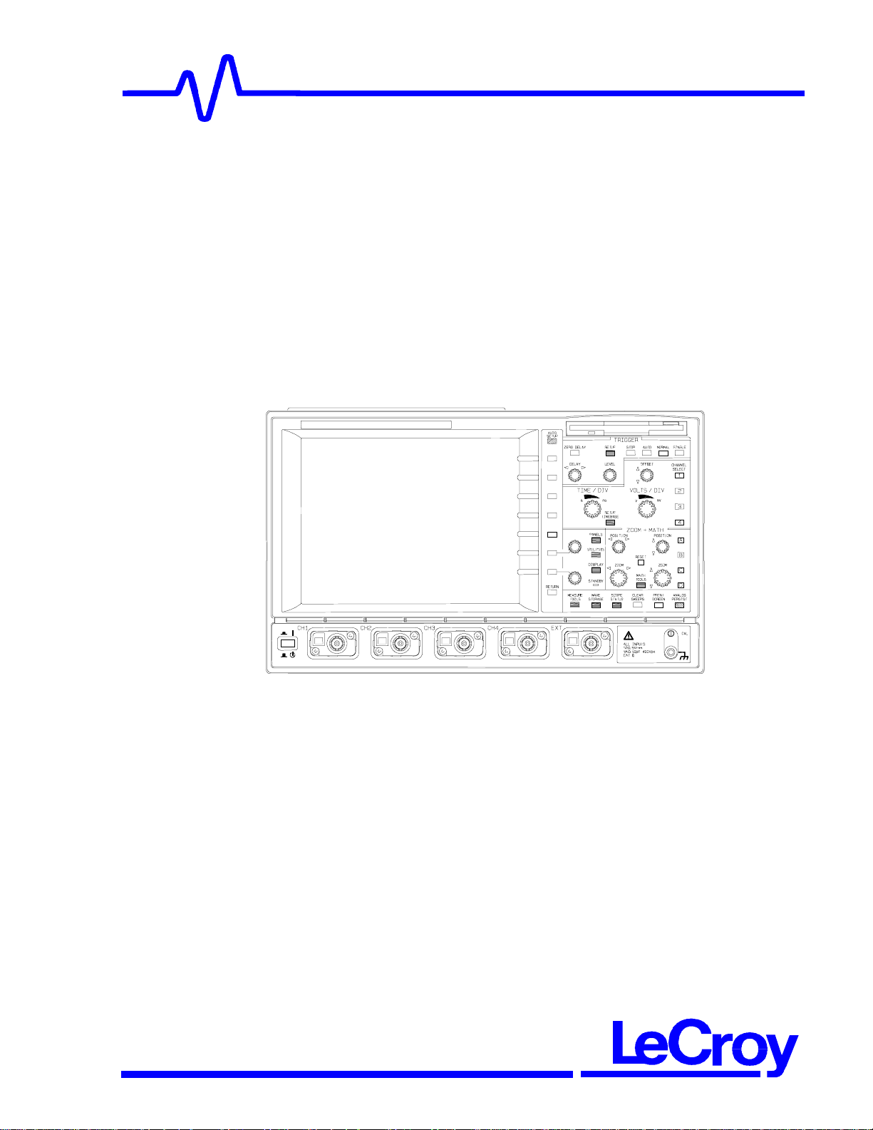
Power On
Connect the oscilloscope to the power outlet and switch it on using the power
On/Standby button, located near the left-hand corner of the instrument below the
screen. After the instrument is switched on, auto-calibration is performed and a test
of the disk drive analyzer's ADCs and memories is carried out. The full testing
procedure takes approximately 10 seconds, after which time a display will appear on
the screen.
2-4 General Information
Page 9

S
pec
ificati
3 Specifications
3.1 Models
Waverunner2 LT372/262 Series: Two channels
Waverunner2 LT584/374/354/264 Series: Four channels
3.2 Vertical System
Bandwidth (−3dB): LT584: 1 Ghz; LT374/372/354:500 MHz; LT264/262:350 MHz @ 50 Ω
Bandwidth Limiter: 20 MHz and 200 MHz can be selected for each channel.
Input Impedance: 50 Ω ± 1.0 %; 1 MΩ ± 1.0 % // 12 pF typical using PP006 probe
Input Coupling: 1 MΩ: AC, DC, GND; 50 Ω: DC, GND
Max Input: 50 Ω: 5 Vrms; 1 MΩ: 400 V max (peak AC <-5 kHz + DC)
Vertical Resolution: 8 bits; up to 11 bits with enhanced resolution (ERES)
ons
Sensitivity (50 Ω or 1 MΩ): 2 mv - 10V/div fully variable
Offset Range:
¾ 2 mV–99 mV/div: ± 1 V
¾ 100 mV–0.99 mV/div: ± 10 V
¾ 1 V–10 V/div: ± 100 V
Isolation - Channel to channel: >250:1 at same V/div settings
3.3 Timebase System
Timebases: Main and up to four zoom traces simultaneously
Time/Div Range: LT374/372/LT584: 500 ps/div 1000 s/div, LT264/262/354: 1 ns/div to
1000 s/div
Clock Accuracy: ≤ 10 ppm
Interpolator Resolution: 5 ps
External Clock: ≤ 500 MHz, 50 Ω, or 1 MΩ impedance
Roll Mode: time/div 500 ms - 1000 s/div or sample rate <100 kS/s max
Specifications 3-1
Page 10
3.4 Acquisition System
Single Shot Sample Rate LT584/M/L LT374/M/L LT372 LT264/M LT262 LT354/M/ML
1 Channel Max 4 GS/s 4 GS/s 4 GS/s 1 GS/s 1 GS/s 1 GS/s
2 Channels Max 4 GS/s 4 GS/s 2 GS/s 1 GS/s 1 GS/s 1 GS/s
3-4 Channels Max 2 GS/s 2 GS/s NA 1 GS/s NA 1 GS/s
Maximum Acq Points/Ch
1 Channel Max 500k/2M/8M 500k/2M/8M 500k 100k/1M 100k 500K/1M/2M
2 Channels Max 500k/2M/8M 500k/2M/8M 250k 100k/1M 100k 500K/1M/2M
3-4 Channels Max 250k/1M/4M 250k/1M/4M NA 100k/1M NA 250k/1M/4M
3.5 Acquisition Modes
Random Interleaved Sampling (RIS): 50 GS/s for repetitive signals 500 ps/div - 1 µs
Single Shot: For transient and repetitive signals: 1ns/div - 1000s/div
Sequence Mode:
LT262/264 2 - 400 segments
LT584/354/372/374 2 - 1000 segments
Memory Option M or L 2 - 400 segments
Intersegment Time 50 µsec max
3.6 Acquisition Processing
Averaging: Summed averaging to 103 sweeps; continuous averaging with weigthing range
range from 1:1 to 1:1023 (standard). Summed averaging up to 10
WAVA)
Enhanced Resolution (ERES): From 8.5 to 11 bits vertical resolution
6
Envelope (Extrema): Envelope, floor, roof for up to 10
sweeps
6
sweeps (optional with
3-2 Specifications
Page 11

3.7 Triggering System
Modes: NORMAL, AUTO, SINGLE and STOP
Sources: Any input channel, External, EXT 10 or line; slope, level and coupling are unique
to each source (except line trigger). Inactive channels useable as trigger inputs.
Slope: Positive, Negative, Window
Coupling Modes: DC,AC,HFREJ,LFREJ
AC Cutoff Frequency 7.5 Hz typical
HFREJ, LFREJ 50 kHz typical
Pre-trigger delay 0 - 100% of horizontal time scale
Post-trigger delay 0 - 10000 divisions
Hold-off by time or events Up to 20s or from 1 to 99,999,999 events
Internal trigger range ±5 div
Maximum Trigger Frequency: Up to 500 MHz (350 MHz on LT264/262)
External Trigger Input Range: ± 0.5 V, ± 5 V with Ext 10
Max external input @ 50Ω: ±5 V DC or 5Vrms
Max external input @ 1MΩ: 400 Vmax (DC + peak AC < 5 kHz)
3.8 Automatic Setup
Auto Setup: Automatically sets timebase, trigger, and sensitivity to display a wide range of
repetitive signals.
Vertical Find: Automatically sets the vertical sensitivity and offset for the selected channels
and display a waveform with maximum dynamic range.
3.9 Probes
Model PP006: PP006 with auto-detect: 10:1, 10 MΩ; one probe per channel
Probe System: ProBus Intelligent Probe System supports active, high-voltage, current, and
differential probes, and differential amplifiers
Scale Factors: Up to 12 automatically or manually selected
Specifications 3-3
Page 12

3.10 Color Waveform Display
Type: VGA Color 8.4-inch flat-panel TFT-LCD
Resolution: 640 x 480 resolution
Screen Saver: Display blanks after 10 minutes (when screen saver is enabled)
Real Time Clock: Date, hours, minutes, and seconds displayed with waveform
Number of Traces: Display a maximum of eight traces. Simultaneously display channel,
zoom, memory, and math traces
Grid Styles: Single, Dual, Quad, Octal, XY, Single+XY, Dual+XY; Full Screen gives
enlarged view of each style
Intensity Controls: Separate intensity control for grids and waveforms
Waveform Styles: Sample dots joined or dots only — regular or bold sample point
highlighting
Trace Overlap Display: Select opaque or transparent mode with automatic waveform
overlap management
3.11 Analog Persistence Display
Analog Persistence and Color Graded Persistence: Variable saturation levels; stores
each trace’s persistence data in memory
Trace Selection: Activate Analog Persistence on a selected trace, top 2 traces, or all
traces
Persistence Aging Time: Select from 500 ms to infinite
Trace Display: Opaque or transparent overlap
Sweeps Displayed: All accumulated or all accumulated with last trace highlighted.
3.12 Zoom Expansion Traces
Style: Display up to four zoom traces
Vertical Zoom: Up to 5x expansion, 50x with averaging
Horizontal Zoom: Expand to 2 pts/div, magnify to 50 000x
Autoscroll: Automatically scan and display any zoom or math trace
3.13 Rapid Signal Processing
Processor: Power PC
Processing Memory: Up to 128 Mbytes
Realtime Clock: Dates, hours, minutes, seconds, and time stamp trigger time to 1ns
resolution.
3.14 Internal waveform Memory
3-4 Specifications
Page 13

Waveform: M1, M2, M3, M4; (Store full-length waveforms with 16 bits/data point)
Zoom and Math: Four traces A, B, C, D with chained trace capability
3.15 Setup Storage
For front panel and instrument status: Four non-volatile memories and floppy drive are
standard; hard drive and memory card are optional
3.16 Interface
Remote Control: Full control of all front panel controls and internal functions via GPIB and
RS-232-C, or Ethernet (optional)
GPIB Port: Full control via IEEE-488.2; configurable as talker/listener for computer control
and data transfer
RS-232-C: Asynchronous transfer rate of up to 115.2 kbaud
Ethernet (optional): 10 Base-T Ethernet interface
Floppy Drive: Internal, DOS-format, 3.5" high-density
PC Card Slot (optional): Supports memory and hard drive cards
External Monitor Port Standard: 15-pin D-Type VGA-compatible
Centronics Port: Parallel printer interface
Internal graphics printer (optional): Provides hardcopy output in <10 seconds
3.17 Outputs
Calibrator signal: 500 Hz–1 MHz square wave or DC level, Select from −1.0 to +1.0 into
1MΩ, output on front panel test point and ground lug
Control signals: Rear panel, TTL level, BNC output, Choice of trigger ready, trigger out, or
Pass/Fail status (output resistance 300 Ω ± 10 %)
3.18 Environmental and Safety
Operating Conditions: Temperature 5–40° C rated accuracy, 0-45°C operating, -20° -
60°C non-operating; humidity 80 % RH non-condensing up to 35° C, derates to 50% max
RH, non-condensing at 45°C; 4500 m (15000ft) max up to 25°C; Derates to 2000 m
(6600ft) at 45°C.
CE Approved: EMC Directive 89/336/EEC; EN61326-1 Emissions and immunity, Low
Voltage Directive 73/23/EEC; EN 61010-1 Product Safety (Installation Category II, Pollution
Degree 2)
UL and cUL: UL Standard UL 3111-1; cUL Standard CSA C22.2 No. 1010-1
Specifications 3-5
Page 14

3.19 General
Auto Calibration: Ensures specified DC and timing accuracy is maintained for 1 year
minimum.
Auto Calibration Time: <500ms
Power Requirements: 90–132 V AC 45-440 Hz, and 180–250 V AC; 45–66 Hz; automatic
AC voltage selection, maximum power dissipation 150 VA–230 VA, depending on model
Battery Backup: Front panel settings retained for two years minimum
Warranty and Calibration: Three years; calibration recommended yearly
3.20 Physical Dimensions
Dimensions (HWD): 210 mm x 350 mm x 300 mm (8.3" x 13.8" x 11.8"); height excludes
scope feet
Weight: 8 kg (18 lbs.)
Shipping Weight: 12kg (27 lbs.)
3.21 Math Tools (Standard)
Simultaneously perform up to four math (signal) processing functions; traces
can be chained together to perform math-on-math.
average (summed to 4000 sweeps) product
Average (continuous weighted) ratio
difference reciprocal (invert)
enhanced resolution (to 11 bits) resample (deskew)
envelope rescale (with units)
FFT of 50 kpoint waveforms roof
floor sin x/x
identity sum
negate
3-6 Specifications
Page 15

3.22 Measure Tools (Standard)
Automated measurements; Display any five parameters together with their average, high,
low, and standard deviations.
amplitude fall 90-10% period
area fall 80-20% Phase
base frequency rise 10-90%
cycle mean maximum rise 20-80%
cycle rms mean rms
cycles minimum sdev
delay +overshoot top
∆delay
duty cycle peak-to-peak xamn
xamx
–overshoot width
3.23 Pass/Fail
Test any five parameters against selectable thresholds. Limit testing is performed using
masks created on the scope or PC. Set up a pass or fail condition to initiate actions such as
hard-copy output, saving waveform to memory, GPIB SRQ, or pulse out.
3.24 Options
Extended math and Measurement: Adds math and advanced measurements for all general
purpose applications. Includes all standard math and measurement tools, plus the
following tools:
3.25 Extended math tools
Automated measurements; Display any five parameters together with their average, high,
low, and standard deviations.
absolute value integrate
differentiate square
exp (base e) square root
exp (base 10) trend (datalog)
log (base e) histogram (200 events)
log (base 10)
3.26 Cursor Measurements
Type From To
Relative time: First point on waveform Any other point on waveform
Relative voltage: Select voltage level Any other voltage level
Absolute time: Time and voltage relative to Ground and trigger
Absolute voltage Voltage Ground
Specifications 3-7
Page 16

3.27 Extended Measure Tools
cycle median first point
∆time@level, % and volts
∆time @level from trigger
∆time from clock to data + (setup
time)
∆time from clock to data - (hold time)
fall @ level, % and volts std. Deviation
duration
last point
number of points
median
rise @ level, % and volts
3.28 WaveAnalyzer
Includes the Extended Math and Measure Tools as well as expanded capabilities for
performing FFT's, averaging, histograms, and histogram paramters.
3.29 WaveAnalyzer Tools (Standard)
Histograms with 18 histogram parameters up to 2 billion events
Summed averaging to one million sweeps
FFT capability expands the basic FFT to include:
FFT power averaging
FFT power density – real and imaginary
FFT on all acquisition points up to 25 Mpts
With Waveanalyzer FFT you get maximum resolution at wide frequency spans.
3.30 Other Application Solutions Available
Jitter and Timing Analysis (JTA)
Digital Filter Package (DFP)
PowerMeasure Analysis (PMA1)
Communications Mask Testing (MT01/MT02)
Polymask Mask Testing (PMSK)
Advanced Optical Recording Measurements (AORM) for LT37X scopes
Disk Drive Measurements (DDM)
PRML Analysis (PRML)
3.31 Free Software Utilities
ScopeExplorer: Easy-to-use utility that provides a simple but powerful way to control your
scope remotely over RS-232-C, GPIB, or Ethernet.
ActiveDSO: Active X controls for flexible Windows applications programming with remote
control.
MaskMaker: Create your tolerance mask offline with this graphic tool.
DSO Filter: Specify a set of filter coefficients offline and load them into the scope.
3-8 Specifications
Page 17

3.32 Basic Triggers
Edge/Slope/Window/Line: Triggers when signal meets slope and level condition
3.33 SMART Trigger Types
State/Edge qualified: Triggers on any input source only if a given state (or transition) has
occurred on another source. Delay between sources is selectable by time or number of
events.
Dropout: Triggers if the input signal drops out for longer than a selected time out between
25 ns and 20 s.
Pattern: Logic combination of 5 inputs (3 on 2 channel models); Each source can be high,
low or don't care. Trigger entering or exiting the pattern.
TV: Triggers selectable fields (1,2,4 or 8) for NTSC, PAL SECAM, or non-standard video
(up to 1500 lines).
3.34 SMART Triggers with Exclusion Technology
Signal or Pattern Width: Triggers on glitches or on pulse widths selectable from <2.5ns to
20 s or on intermittent faults.
Signal or Pattern Interval: Triggers on intervals selectable between 10 ns and 20 s
Slew Rate: Triggers on edge rates; select limits for dV, dt, and slope. Select edge limits
between 2.5ns and 20s.
Runt: Positive or negative runts defined by two voltage limits and two time limits
selectable between 2.5 ns and 20 ns
3.35 Hardcopy
Print Screen is activated by a front-panel button or via remote control. Store screen image
files or print to external printers including network printers and directories. Netwrok printing
and file access requires the LAN10BT Ethernet option.
Supported printers include:
B/W: LaserJet, DeskJet, Epson. An optional, internal high-resolution graphics printer is also
availablefor screen dumps; stripchart output formats capable of up to 200 cm/div.
Color: DeskJet 550C, Epson Stylus, Canon 200/600/800 series, HP7470 and HP7550
Hard copy Formats: TIFF b/w, TIFF color, BMP color, BMP compressed and HPGL
3.36 Waveform Output
Store waveforms to floppy disk or optional PC-Card hard drives and memory cards.
Save any trace you choose and select Auto Store to automatically store the waveform after
each trigger.
Output Formats: The ASCII waveform output is compatible with spreadsheets, MATLAB,
MathCad, etc. Binary output is also available for reduced file size.
Specifications 3-9
Page 18

3.37 Documentation
Included with all WavePro Oscilloscopes: Operations Manual — hard copy, Remote
Programming Manual — hard copy, CD-ROM — PDF formatted manuals plus software
utilities including: ScopeExplorer, ActiveDSO, MaskMaker, DSO-Filter and DSO-Net Print
Gateway.
3-10 Specifications
Page 19

4. Theory of Operation
4.1 Processor Board
MPC603e Processor
The PowerPC603e on the processor board is a 64-bit RISC processor having
2x32Kbyte cache and features high speed processing and quick memory access.
The processor is designed to operate with an internal clock which is 5 times the
external bus clock cycles and is used under the 32bit mode.
The board consists of two circuit-blocks:
• The 32bit block, that contains the main PowerPC processor, synchronous
dynamic RAM module, VGA interface, Super-I/O and main board interface.
• The 8bit block, which incorporates all peripherals and other interfaces for outer
connections.
These two circuit-blocks are connected through MC68150 (dynamic bus sizer).
Power Supply
The board requires two power sources (Vcc and +12V). +12V source is used for
OP-amps and small-peripheral operation.
The processor requires 3.3V and 2.5V, and some other logic devices are operated
by the +5V source. All of the signals are TTL compatible.
An OP-amp and MOSFET transistor comprise the 3.3V and 2.5V power source. The
reference voltage is taken through the voltage-resistor divider network across the
+5V power source.
32bit Peripherals
There are 5 devices on the processor’s 32bit data bus:
• VGA video controller
• S-DRAM system
• bus sizer, an interface to 8bit circuit-block
• Super-I/O
• MAIN board
Theory of Operation 4-1
Page 20
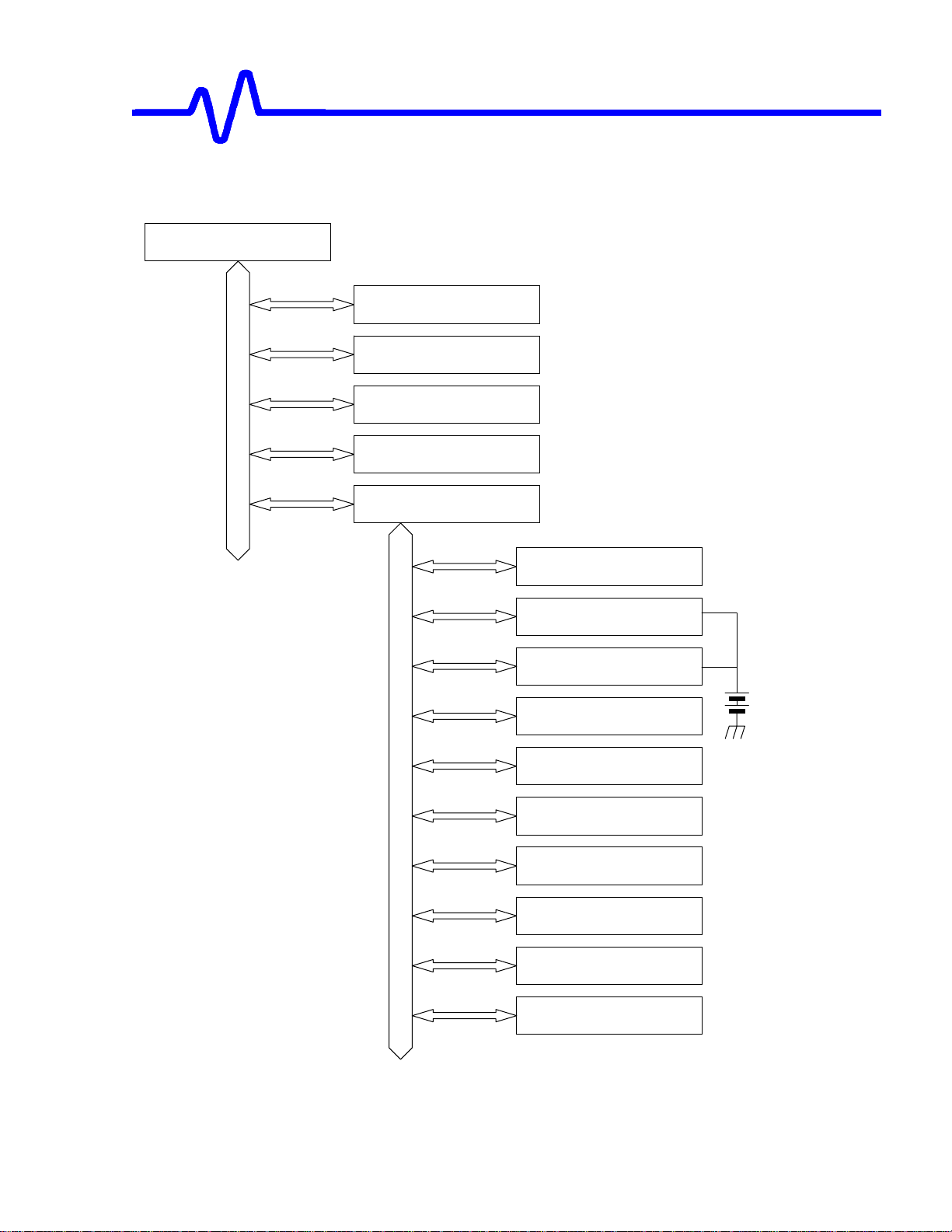
CPU’s Block Diagram
CPU : PowerPC603e
32bit BUS
SDRAM max 512MB
Super I/O
RS232C, Parallel, Floppy
MAIN Board I/F
VGA : 65545
BUS Sizer :
Flash PROM :
NVRAM : 128KB
Real Time Clock
Interrupt Controller
Front Panel I/F
GP-IB
Internal Printer I/F
Small Peripherals
PCMCIA type I/II/III
Other Control Ports
8bit BUS
Figure 4-1 CPU Block Diagram
4-2 Theory of Operation
Page 21

SDRAM
The SDRAM circuit consists of one DIMM module, from 64MB to a maximum of
512MB. The DIMM module type is 168pin SDRAM, 3.3V unbuffered CL=2. The
SDRAM control circuit is built with one CPLD, and several gate ICs.
The SDM (IC87) located on the main control circuit generates all types of bus cycle
timing (normal R/W, 2-beat/8-beat bursts of R/W), refresh cycles. Furthermore, the
SDM has a register for setting the DIMM size, in order to adjust the memory
mapping so as not to have gaps in memory mapping according with the memory
capacity. Two multiplexers (IC9 and IC10) switch the address lines of odd and even
addresses to be connected with the address lines of each DIMM.
Normal Access Timing
This is the simplest access possible: the processor puts an address onto the
address bus and reads or writes the required data out of or to the SDRAM which
corresponds with the bus. The bus width is 32bits, or 4bytes wide, and the CPU
performs to read or write operations (of one through four bytes) which are chained in
a bus cycle.
Burst Access Timing
A burst access, on the 603e configured with 32bit device operation, performs either
two or eight successive reads in SDRAM (2-beat or 8-beat burst access). The idea
is to put the beginning of an address onto the address bus and read/write data out of
or to the SDRAM every clock cycle, without incrementing the address required by
the processor (this is to be achieved by the SDRAM's Burst mode). The 8-beat
access is indicated by an active "low" of NTBST signals and a 32bit access signal
(SIZ2..0=011), and the 2-beat access is indicated by an active "high" of NTBST
signals and an access size of 64 bits (SIZ2..0=100).
Refresh Timing
The 32 KHz clock from the RTC chip is used to generate the timing to refresh
SDRAM. Without this clock, the SDRAM would not be refreshed and all the data in it
would be erased. SDM detects the rising edge and the falling edge of this 32KHz
clock. At the each edge, it generates the refresh cycles.
The arbitration logic between other accesses (bus cycle with the processor and DMA
cycle) and refresh cycles reside in the SDM.
Theory of Operation 4-3
Page 22

Memory Mapping
When power is turned on, the internal software automatically sets the system's
memory size to the largest capacity available with the DIMM that is installed (64MB 512MB DIMM size).
VGA controller
The VGA controller chip 65545(IC29) contains the logic circuits to decode its own
addresses. It generates all the video signals (RGB, H/V, and all control lines to drive
the flat panel), and controls its associated 1 MB video DRAM (to read, write and
refresh). There are two 2Mb video DRAMs mounted but only 512KB of each of the
DRAM's is used.
All timings are extracted from the 16MHz bus clock; therefore, no external crystal or
time-base is required. The horizontal and vertical synchronization signals are sent
to the external video connector (a half pitch, D-SUB15 pin connector is used).
The 65545 chip can support several bus interfaces (PCI, ISA, VL, etc), the system
employs it for VL-bus applications with the mode of 256-color palette operations.
The controller has an 18bit color palette and can display 256 colors out of the
available 260,000.
The power supply circuit for the liquid crystal panel has a MOSFET switch that
switches the power supply of LCD to 3.3V or 5V.
Also the VGA controller has a switch, it switches the max signal level for the LCD to
3.3V or 5V.
Super-I/O
This device controls RS-232C, floppy disk, and parallel port operations. The
controller has its own time-base with a 24MHz crystal. RS-232C can be used by
simply connecting the MAX232 buffer (IC31) to it. Since the Super I/O chip has a
16-byte buffer, high speed data transfer is easily carried out.
A 2HD disk drive can be directly connected to the system without any external
components other than a pull-up resistor; it can be operated in interruption mode.
The parallel interface is also activated without other external components other than
a pull-up resistor, for the use of 2-way communication.
Bus Control
The BUS (IC93) performs all bus cycles except those for SDRAM. When the bus
cycle starts, the MPC603e must terminate the bus cycle by returning signals after
acknowledging each of the data and addresses, from the outside. The BUS is used
to generate the acknowledgement signals.
4-4 Theory of Operation
Page 23

Bus Sizer
The MPC603e processor does not support dynamic bus sizing, which is performed
with the 68K processor family. Each 8bits of the 32bit bus is fixed or assigned with
the lower addresses, or 0 through 3 bits. Therefore, if an 8bit device were directly
connected to the bus, this device would be seen in 4byte steps each in the memory
map area. To avoid this, the 8bit-bus peripheral unit is connected to the 32bit-bus
through the bus sizer, MC68150 (IC15). The bus sizer divides one bus cycle for
accessing 32 bit-bus of the processor into four cycles each of 8bit accessing cycle,
and/or assigns 8bit-bus data to a corresponding 8bits within the 32bits.
8bit Peripherals
The following devices are listed as 8bit data bus units:
• PCMCIA Interface
• Flash PROM
• NVRAM
• RTC
• Interrupt Controller
• GPIB Interface
• Small-peripherals Interface
• Internal printer Interface
• Front-Panel I/F
• Other registers and ports
PCMCIA, type I/II/III interface
This interface consists mainly of buffers for both data and address busses. IC65 (DF/F) holds control bits for the signals resetting the card, switching between the data
area and the attribute area, and switching the card's modes. All bits in the register
are reset to zero when the _RESET signal goes to active low, which means that their
state is also guaranteed at power-up.
IC66 and the IC67 invert the most significant address bits of the memory card
whenever the SWAP jumper is plugged in, so that the first bytes are always
allocated to "FFF00000", regardless of the size of the memory card. This allows the
processor to boot directly from the PCMCIA memory card used.
Flash PROM
Two pieces of Intel's 29F016-compatible 2MB PROMs (IC45 and 46) are used.
These ICs do not require any programming voltage to write. From a hardware point
of view, a flash PROM is regarded the same as an EPROM in read mode. To erase
or write to memory, commands are written into the data bus. Writing and erasing
must be performed by monitoring the status-signals (RY/#BY) on the port (IC49).
The program may be seen to start from the Flash PROM. The Flash PROM is,
however, not regarded as the program or its program area even when start-up (even
Theory of Operation 4-5
Page 24

when the screen appears) is completed, because the program must be processed in
the SDRAM after transferring the program content from the Flash PROM into the
SDRAM.
NVRAM
This memory chip is powered from V
the NVRAM is powered by the lithium battery, when it is on, it is powered from V
in the RTC. When the main power is off,
CCO
CC
.
The #CS1 signals are also controlled by the RTC. When the main power is turned
off, the RTC sets the chip select "high" to place the SRAM in power-down mode to
prevent any accidental overwriting. Stored panel setups (Setup1 - 4), the
instruments last panel setup and trace memories M1-M4 are stored in the NVRAM.
RTC
The DS1689 real time clock has several functions:
• Keeps the time-of-day and current-date information while power is off.
• Generates the 32KHz clock for SDRAM refreshing.
• Generates a 128Hz periodic interrupt signal to force bus accessing from
the processor and allow periodic updating of the time display.
• Provides a unique ID that identifies the origination of scope ID.
• Feeds the power and the chip select signal to the NVRAM.
The RTC chip generates timing clocks necessary for time keeping and other circuits
using a 32.768KHz crystal. A few discrete components around the RTC leave it
powered by the lithium battery when the system is turned off. When the system is
turned on this circuit charges the battery. Accesses from the processor are done
through bus separation circuit, since addresses and data are multiplexed. A unique
ID is written into the RTC by the RTC manufacturer, since every chip must have a
different value stored in it.
4-6 Theory of Operation
Page 25

Interrupt Controller
In order to prioritize and control several interrupt sources, it is necessary to use an
IC of uPD71059. It scans eight interrupt signals and sends a unique interrupt signal
to the processor when an (unmasked) interrupt signal appears.
Interrupt levels are assigned as follows:
level 0 (lowest priority) FDC
level 1 small peripherals
level 2 RS232C
level 3 GP-IB
level 4 PCMCIA (I/O card mode)
level 5 real time clock
level 6 the MAIN board
level 7 (highest priority) unused
The priority in the above can be changed by the software.
Small Peripheral Interface
This 8-bit interface is intended to allow external expansion of the board in addition to
the processor board. The tri-state buffers drive the address and control lines, and
bi-directional buffers drive data lines. The address decoding is processed on each
expanded peripheral board. Since the acknowledgement toward each access is
also returned by the expanded board, there is no restriction to the amount of waitstates. The bus clock runs at 16MHz, and a reset line reinitializes the boards as
does the CPU. Four interrupt lines are also included in this interface, so that
interrupt-driven boards can be used.
Front Panel
The front panel is accessed by serial read/write signals passing through IC47 and
IC48. The CPU board can be reset by resetting the 3 buttons on the front panel.
This function becomes effective by setting a bit of IC52 for enabling. Both the LED
and the beeper are activated by serial writing.
Reset Circuit
When the power supply is turned on and V
exceeds 4.5V, IC4 detects this and
CC
starts generating the clock (IC2) After the clock is stabilized and counted 1024
times, the reset signal is released by IC86 after the time determined by C167.
Whenever V
goes below 4.5V (even for a very short time), a reset pulse, in which
CC
the width is determined by C6, is generated. Resetting 3 buttons on the front panel
also cause the reset pulse as did IC4 when the supply power voltage fell too low.
Theory of Operation 4-7
Page 26

Bus Error Generation
The MPC603e expects NTA and NAACK signals for acknowledgement to the current
bus cycle, and inserts wait states during the period NTA and NAACK are kept at
“high” levels (any of external devices have not pulled these signals "low"). As long
as any of the devices do not return the acknowledgement, the bus is kept in this
wait-condition. An external circuit is then required to generate a bus-error signal to
break the pending cycle after a given time-out. The bus error is generated by pulling
the NTEA pin of the CPU down to “low”. This job is done by the BUS (IC93) which
counts the number of wait-states that have already passed through the counter.
With this operation, the system can successfully force the termination of the current
cycle. Some devices, such as the VGA video controller, have their own logic to
generate a bus error. Therefore, any access operations for those devices do not
need this circuit.
GPIB Interface
GP-IB controller is the National Instrument’s NAT4882. It has NEC-7210 software
compatible made and it includes bus drivers.
Internal Printer Interface
Printer control is the same as for the normal Centronics interface. This circuit
consists of buffers only.
4-8 Theory of Operation
Page 27
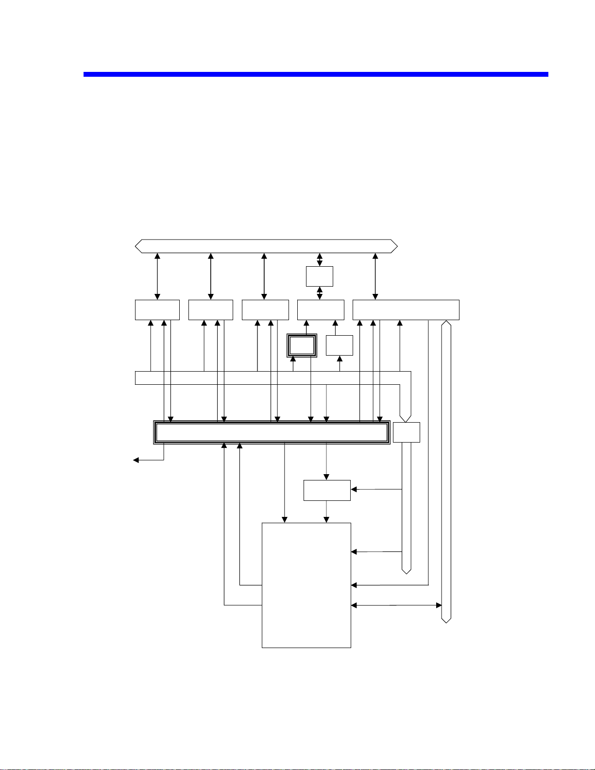
Relation of I/O Structure to the associated CPLDs
The following block-diagram describes the flow in the decoder and the relationships
between the acknowledgement to be returned to the CPU and CPLDs.
Three-line boxes are CPLDs, and one-line boxes indicate other ICs and function
blocks.
• SDM does all the controls for the access of the SDRAM (Initialize memory,
Decode and Mapping, Read/Write, Burst Read/Write, Refresh).
• Bus controls is the bus cycle of the entire CPU board. (Decode all areas other
than SDRAM, Read/Write of 32bits bus, Read/Write of the bus via bus sizer,
detection of bus error).
CPU BUS (Data)
Buffe
VGA Supper MAIN SDRAM
CPU BUS
To CPU
Decoder
71059
GP-IB (16bit)
NVRAM
RTC
Small Peripherals
Front Panel
Flash ROM
PCMCIA (16bit)
BUS sizer
MUX
Buffe
Address
Figure 4-2 I/O Structure
Theory of Operation 4-9
Page 28

4.2 Main Board
Introduction
The main board is divided into the following sections:
• Front End
Based on the Hybrid HFE428, HSY632 switchyard to combine the input
channels.
• A/D Converter & Digital Acquisition Memory
Based on the HAM631.
• Trigger
Based on the Hybrids HTR420 discriminator & MST429A smart trigger.
• Timebase
Based on the MCG426 clock generator & MTB411A controller
• Main Board Control
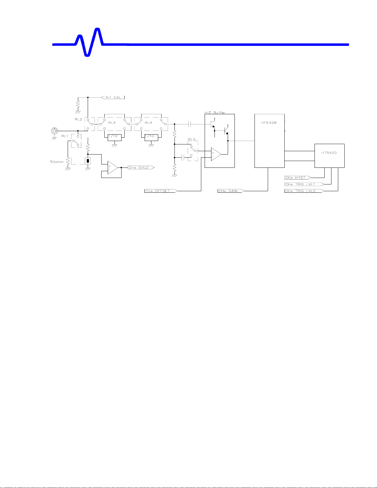
4.2.1 Front End
The front end processes an analog signal for ADC and trigger, consists of High
impedance buffer, amplifier HFE428, and trigger comparator HTR420.
The main functions of the Front end without the amplifier HFE428 and HTR420 are:
• Four channels opertion, calibration with Software control.
• Input protection (clamp+thermal detection) and coupling (AC, DC, 1MΩ, 50Ω).
• Attenuator by 10 & by 100.
• Offset control.
• Offset control of ±1V and CAL control of ±1.4V.
• Detection of 50Ω over loading.
• Input of signal for calibration.
The main functions of HFE428 are:
• Amplitude normalization for the ADC system : at the BNC the dynamic range is 16
mV to 80V FS (full scale) and the ADC/TRIG system input is 500 mV differential.
• Fine adjustment of gain and variable control
• Band width limiter of 20MHz, 200MHz
Main function of HFE420 are:
• Generation of trigger signal (analog input and digital output) with comparator
• Setting of trigger level (TRIG,VALIDATE)
• Setting of trigger coupling (DC,AC,LFREJ,HFREJ,HF)
• Setting of slope (+,-,WINDOW)
4-10 Theory of Operation
Page 29

Control
Relay control
The relay of the attenuator is set by selecting the input coupling and the gain as shown in
the table below.
RL1, 2 and 5 are driven with +5V/0V, and RL3, 4 is driven with +5V/-5V.
Input coupling
Control port Relay GND 1M,DC 1M,AC 50,DC
GND/*MES RL2 H L L L
1M/*50 RL1 H H H L
AC/*DC RL5 H L H L
1/*10 RL3 H X X X
1/*100 RL4 L X X X
Switch of attenuator
Control port Relay 2mV-99mV 100mV-0.99V 1V-10V
1/*10 RL3 H L L
1/*100 RL4 H H L
Divide gain
The gain ratio in each block and input range is a table below.
At the BNC the dynamic range is 16 mV to 80V FS (full scale) and the output is 500 mV
differential (HAD631 input).
Range V/div
Block
ATT 1/*10
ATT 1/*100
HFE428
Total(ratio)
2mV 5mV 10mV 20mV 50mV 100mV 200mV 500mV 1V 2V 5V 10V
1 1 1 1 1 0.1 0.1 0.1 0.1 0.1 0.1 0.1
1 1 1 1 1 1 1 1 0.1 0.1 0.1 0.1
31.25 12.5 6.25 3.125 1.25 6.25 3.125 1.25 6.25 3.125 1.25 0.625
31.25 12.5 6.25 3.125 1.25 0.625 0.3125 0.125 0.0625 0.03125 0.0125 0.00625
Analog control voltage
Circuit name signal level Signal name
CHx OFFSET +/-4V Offset control signal
CHx GAIN 0 to +4V HFE428 gain control signal
CHx TRIG LVL1 +/-4V Trigger level control signal
CHx TRIG LVL2 +/-4V Trigger level control signal for smart trigger/window
CHx HYST 0 to +4V Trigger hysteresis control signal
INT CAL 0 to +600mV Signal each CH commonness for calibration
Theory of Operation 4-11
Page 30
Block diagram 1
HAM631
4-12 Theory of Operation
Page 31

4.2.2 Acquisition Block Diagram
429
MST
TDC
32-bit
426
MCG
TIME BASE
MTB
411A
Time Base Control
MAM
MAM
MAM
MAM Control
Digitizer System
MAM
MTR
HTR420
Trigger Comparator
633
442
MAD
633
442
MAD
633
442
MAD
633
442
MAD
418
TRIGGER/
5x
443
MSY
443
MSY
EXTERNAL
EXTERNAL CLOCK
7
MFE43
HFE428
FRONT END D
7
MFE43
HFE428
FRONT END C
32-bit
Serial Bus
7
MFE43
HFE428
FRONT END B
7
MFE43
HFE428
FRONT END A
32-bit
Digitizer System
MAM
633
MAM
633
MAM
633
MAM
HAM631
MAD
MAD
MAD
443
MSY
442
442
443
MSY
442
HSY632
442
633
MAD
Theory of Operation 4-13
Page 32

4.2.3 Control & Transfer Block Diagram
Processor
PowerPC
System Memory
SDRAM
Processor Bus
FRONTEND
HFE428 A
Digitizer System
MAM
MAM
633
633
MAD
MAD
442
442
MSY
443
(ReadOut Plus Min-Max)
RPM
32-bit
32-bit
MAM
MAM
633
633
MAD
MAD
442
442
MSY
443
FRONTEND
HFE428 B
Serial Bus
MAM Control
Digitizer System
MAM
633
MAD
442
MSY
443
FRONTEND
HFE428 C
MAM
633
MAD
442
32-bit
MAM
633
MAD
442
MSY
443
MAM
633
MAD
442
FRONTEND
HFE428 D
4-14 Theory of Operation
Page 33

4.2.4 Channel Mode
4ch mode(LT374)
A
HFE428 HAM631
B
X
C
HTR420
A
HFE428
B
X
C
HTR420
A
HFE428 HAM631
B
X
C
HTR420
HSY632
MSY443
MSY443
HSY632
MSY443
HAM631
HAM631
HAM631
HAM631
LT264
HFE428
HFE428
HFE428
A
B
C
A
B
C
A
B
HAM631
X
HTR420
HAM631
X
HTR420
HAM631
X
HFE428
A
B
X
C
HTR420
MSY443
HAM631
HAM631
2ch mode(LT374)
A
HSY632
HFE428 HAM631
B
X
MSY443
HAM631
HAM631
MSY443
HAM631
HFE428
C
HTR420
A
B
X
C
HTR420
A
HSY632
HFE428 HAM631
B
X
MSY443
HAM631
HAM631
MSY443
HAM631
HFE428
C
HTR420
A
B
X
C
HTR420
HFE428
C
HTR420
A
B
C
HAM631
X
HTR420
Theory of Operation 4-15
Page 34

4.2.5 µP Control
Control between the microprocessor and the main board is accomplished via the
RPM. The RPM functions are:
• Processor interface
• MAM interface
• 8 bit bus interface (MTB411, MCG426, MST429A, IIC)
• Serial interface
• Min-Max Computation
• Histogram
• RPM is configured at boot up by the processor. The RPM configuration program
is stored in the flash memory.
4.2.6 Trigger
The different trigger couplings are :
• DC
• AC : cut off frequency is almost 7.5 Hz.
• LF REJ : single pole high pass filter with a cut off frequency at 50
kHz.
• HF REJ : single pole low pass filter with a cut off frequency at 50 kHz.
• HF : frequency divider by four.
Analog Controls
A sample and hold fed by the precision DAC provides the threshold levels. A
precision DAC is also used for a successive approximation ADC which measures
Probus inputs, temperature, etc.
4.2.7 Analog to Digital Converter
Introduction
The analog to digital converter system does the signal conversion to 8 bits, using
the following circuits:
• HSY632: Hybrid switching AMP 2 in 4 out.
• HAM631: Hybrid ADC 1GS/s with 4Mb memory. Provide 83 MHz clock for
memory and refresh for DRAM
4-16 Theory of Operation
Page 35

_
4.2.8 Time Base
The time base includes three circuits:
Trigger circuitry Frequency divider
Block Diagram
Introduction
• MCG426: generates sampling clocks: 12.5 MHz up to 2GHz
generates clocks for the MTB411
interleaves sampling clocks to increase sampling rate and memory
depth.
• MTB411A: Time Base System
TDC interpolator and Real Time computation
• MST429A: Single source trigger, Standard trigger, Hold off, Pulse width & interval
Multiple source trigger, State qualified, Edge qualified
ENABLE TRIGEN
QQD
CONTROL
from uP
to trigger selection
enable
clock 10MHz
DIO(7:0) +
A(1:0) +
control
EXTCK
EXTREF
Vcc
10 MHz
Reference
MST 429
2
TRIG
2
TRIG
S2EDGE
EN10MHZ
10MHZclock 10MHz
500MHZclock 500MHz
TRTTRT
EXTCK
EXTREF
INTREF
PHDET
2
2
RAMPST
MCG 426
VCO
BCK
R
IT
RT
TR
A
C
C
IG
M
D
PS
FDCK
FDEND
MACQ
TSCK
TBCK
SHCK_A
SHCK_B
SHCK_C
SHCK_D
MCLR CLR
VCO2G PDCK
2
2
ITBUSY
TRIGD
ITCK
MTB 411
RTCK
INT
FDCK FDEND
TSCK TBCK
2
SHCK_A
2
SHCK_B
2
SHCK_C
2
SHCK_D
Peak
Detect
MPD
MACQ
HSH & ADC
ITMB
to uP
MEMORY
MCK
MCK
DIN[7..0]
Time Base Block Diagram
Theory of Operation 4-17
Page 36

4.3 Power Supply
Do not touch any electric parts inside the power supplies during operation as the
primary side of the power unit has many high voltage portions to ground.
Input Voltages
The power supply supports a wide ranges of inputs, 90-132 V AC (45-440Hz) and 90-264V
AC (45-66Hz) are allowed.
Output voltages: 9 different DC voltages are available, +5Vd, +12Vd, +12V, and +27V,
+2.5Va, +5Va, -5Va, +12Va,–12Va.
Overview
The power supply unit consists of, roughly divided, Input Circuit, Input Filter & Rectification,
Power Factor Correction, Main Converter (for digital circuits) , Main Converter (for analog
circuits) and output regulators.
Power Switch
A power switch is located on the secondary side. In order to switch -on and -off all of the
outputs on the secondary side; the control is made by switching on and off the main
converter. When the power switch is off, some power is being fed to some components in
the power supply unit (stand-by mode) as long as the unit is plugged into an AC source.
Cooling
The power supply is designed to use forced air cooling with a fan. Operating the power
supply without a fan will cause the over-temperature protection circuits to trip because of
the temperature rise in the unit. When the protection circuit trips the power outputs will be
turned off.
4-18 Theory of Operation
Page 37

5. Performance Verification
5.1 Introduction
This chapter contains procedures suitable for determining if t he LT584, LT374/372,
LT264/262 and LT354 Digital Storage Oscilloscope performs correctly and as
warranted. They check all the characteristics listed in subsection 5.1.1.
Because they require time and suitable test eq uipm ent, you may not need to
perform all of these pr ocedures, depending on what you want to accomplish.
This manual performance verif icat ion procedure can be followed to establish a
traceable calibration. I t is the calibrating entities’ responsibility to ensur e t hat all
laboratory standards used to perform t his procedure are operating within their
specifications and traceable to req uir ed standards if a traceable calibration
certificate is to be issued f or the Digital Storage O scilloscope.
5.1.1 List of Tested Characteristics
This subsection lists the characteristics that ar e tested in terms of quant ifiable
performance limits.
Input Impedance
•
Leakage Current
•
Noise
•
DC Gain Accuracy
•
Offset Accuracy
•
Bandwidth
•
Trigger Level
•
Smart Trigger
•
Time Base Accuracy
•
5.1.2 Calibration Cycle
The LT584, LT374/372, LT 264/262 and LT354 Digital Storage O scilloscope
requires periodic verification of per formance. Under normal use (2, 000 hour s of
use per year) and environmental conditions, this instrument should be calibr ated
once a year.
Rev. D Performance Verification 5-1
Page 38

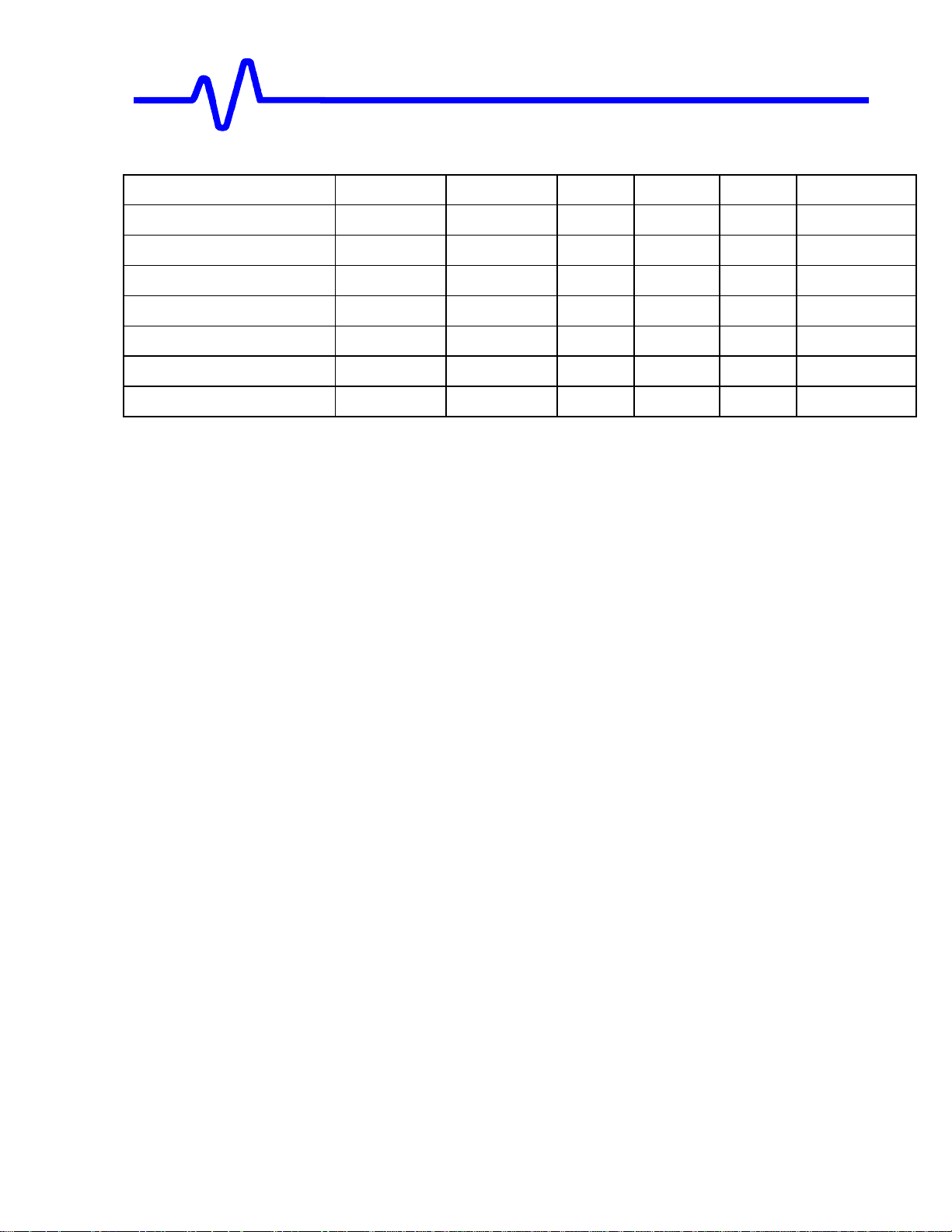
5.2 Test Equipment Required
These procedures use external, traceable signal generators, DC precision power
supply, step generator and digital multimeter, to directly check specifications.
Instrument Specifications Recommended
Signal Generator
Radio Frequency
Signal Generator
Audio Frequency
Voltage Generator
DC Power Supply
Power Meter +
Sensor
Digital Multimeter
Volt & Ohm
Coaxial Cable, 1 ns
Coaxial Cable, 5 ns
2 Attenuators, 20 dB
Attenuator, 6 dB
Terminator, 2 W
T adapter
Frequency : .5 MHz to 2 GHz
Frequency Accuracy : 1 PPM
Frequency : 0 to 5 kHz
Amplitude : 8 V peak to peak
Range of 0 to 20 V, in
steps of no more than 15 mV
Accuracy ±1 %
Voltmeter Accuracy : 0.1 %
Ohmmeter Accuracy : 0.1 %
50Ω, BNC, length 20 cm,
50Ω, BNC, length 100 cm,
50Ω, BNC, 1 % accuracy
50Ω, BNC, 1 % accuracy
50Ω, BNC, Feed-Through
50Ω, BNC T adapter
HP8648B
or equivalent
LeCroy LW420
or HP33120A or
equivalent
HP6633A
or equivalent
HP437B + 8482A or
equivalent
Keithley 2000
or equivalent
LeCroy 480232001
LeCroy 480020101
LeCroy 402200402
LeCroy 402600403
LeCroy 402323001
LeCroy 402222002
Table 5-1 : Test Equipment
5.2.1 Test Records
The last pages of this document cont ain t est records. Keep them as masters and
use a photocopy for each calibration.
5.3 Turn On
If you are not familiar with operat ing the LT584, LT374/372, LT 264/262 or LT354,
refer to the operator ' s m anual.
Switch on the power using the power switch.
!
!
Wait for a minim um of 20 minutes for the scope to r each a stable operating
!
temperature, and verify:
The PNL files used depends on the scope model. The LTxxx represents the LT 262, LT264,
LT354, LT372, LT374.
For the LT584 use the LT374 files.
5-2 Performance Verification Rev. D
Page 39

5.4 Input Impedance
The impedance values for 50Ω and 1MΩ couplings are measured with a high
precision digital multimeter. The DMM is connected to the DSO in 4-wire
configuration (input and sense), allowing for accurate measurements.
Specifications & Test limits
DC 1.00 MΩ ±1 %
AC 1.20 MΩ ±1 % (2mV/div to 99mV/div)
1.00 MΩ ±1 % (100mV/div to 10V/div)
DC 50Ω ±1 %
5.4.1 Channel Input Impedance a. DC 1M
Recall
!
Panel Setups :
Channels Trace OFF
Input Coupling :
Input gain :
Time base :
Trigger mode :
ΩΩΩΩ
xxxP001.PNL
or configure the DSO:
Recall FROM DEFAULT SETUP
Channel 1, Channel 2, Channel 3 & Channel 4
DC 1M
50 mV/div.
50 nsec/div.
Auto
on all 4 Channels
ΩΩΩΩ
on all 4 Channels
Rev. D Performance Verification 5-3
Page 40

Set the DMM with
!
Connect it to Channel 1.
!
Ohms and Ohms sense
to provide a 4 wire measurement.
Measure the
!
limits.
Repeat the above test for all input channels.
!
Recall
!
Repeat the test for all input channels.
!
Record the measurements in Table 2, and compar e the test results to the
!
limits in the test record.
b. AC 1M
Recall
!
and for each Channel make the following change:
Input Coupling :
input impedance
xxxP002.PNL
ΩΩΩΩ
xxxP003.PNL
. Record it in Table 2, and compare it to the
or Set Input gain to
or configure the DSO as shown in 5.4.1. a,
AC 1M
ΩΩΩΩ
200 mV/div.
on all 4 Channels
5-4 Performance Verification Rev. D
Page 41

For all input channels measur e the
!
Record the input impedance in Table 2, and compare it to the lim it s.
!
input impedance
.
Recall
!
Repeat the test for all input channels.
!
Record the measurements in Table 2, and com par e the results to the limits in
!
the test record.
c. DC 50
Recall
!
and for each Channel make the following change:
Input Coupling :
xxxP004.PNL
ΩΩΩΩ
xxxP005.PNL
or Set Input gain to
or configure the DSO as shown in 5.4.1. a,
DC 50
ΩΩΩΩ
200 mV/div
on all 4 Channels.
For all input Channels, measure the input impedance.
!
Record the
!
Recall
!
Repeat the test for all input channels. Record the measur ements in Table 2,
!
and compare the results to the limits in t he test record.
input impedance
xxxP006.PNL
or set Input gain to
in Table 2, and compare it to the lim it s.
200 mV/div.
on all 4 Channels
5.4.2 External Trigger Input Impedance
Rev. D Performance Verification 5-5
Page 42

a. DC 1M
ΩΩΩΩ
!
Recall
xxxP007.PNL
Trigger mode :
Select Setup trigger
Trigger on :
Cplg Ext :
External :
Time base :
or configure the DSO :
Auto
EXT
DC
DC 1M
50 nsec/div.
ΩΩΩΩ
Connect the DMM to External, and measure the
!
Record the input impedance in Table 2, and compare it to the limits.
!
Recall
!
Measure the
!
Record the test result in Table 2, and com par e the result to the limits in
!
the test record.
b. DC 50
5-6 Performance Verification Rev. D
xxxP008.PNL
input impedance
ΩΩΩΩ
or set trigger to Ext/10
.
input impedance
.
Page 43

!
Recall
xxxP009.PNL
Select Setup trigger
or configure the DSO:
Trigger on :
External :
EXT
DC 50
ΩΩΩΩ
Connect the DMM to External, and measure the
!
Record the input impedance in Table 2, and compare the result to the limit in
!
input impedance
.
the test record.
Rev. D Performance Verification 5-7
Page 44

5.5 Leakage Current
The leakage current is tested by measuring the voltage across the input channel.
Test limit
DC 1MΩ : ±1 mV
5.5.1 Channel Leakage Current
!
Recall
xxxP010.PNL
Panel Setups :
Channels Trace ON
Input Coupling :
Input gain :
Trigger mode :
Time base :
or configure the DSO:
Recall FROM DEFAULT SETUP
Channel 1, Channel 2, Channel 3 & Channel 4
DC 1M
50 mV/div.
Auto
10
µµµµ
on all 4 Channels
ΩΩΩΩ
on all 4 Channels
sec/div.
Set the DMM to measure Volts, and connect it to Channel 1.
!
Measure the
!
Repeat the test for all input channels.
!
5-8 Performance Verification Rev. D
voltage
and enter it in Table 3. Compare it t o the limits.
Page 45

5.5.2 External Trigger Leakage Current
a. DC 50
!
and make the following changes :
!
!
ΩΩΩΩ
Recall
Connect the DMM to External.
Measure the
xxxP011.PNL
Select Setup trigger
Set Trigger on :
External :
voltage
or configure the DSO as shown in 5.5.1
EXT
DC 50
and enter it in Table 3. Compare it t o the limits.
ΩΩΩΩ
Rev. D Performance Verification 5-9
Page 46

5.6 Noise
Noise tests with open inputs are executed on all channels for both 1MΩ and 50Ω input
impedance, with AC and DC input coupling, 0 mV offset, at a gain setting of 5mV/div.,
and different Time base settings.
The scope parameters functions ar e used t o m easure the RMS amplitude.
5.6.1 Rms Noise
Test limits
0.5 mV rms at 10 mV/div LT37x
0.45 mV rms at 10 mV/div LT354, 26x.
Procedure
a. DC 1M
With no sig nal connect ed to the inputs
Recall
!
Panel Setups :
Channels Trace ON
Input Coupling :
Input gain :
Trigger setup :
Trigger on :
Coupling 1 :
Trigger Mode :
Time base :
Channel use :
Record up to
Press :
Measure :
Mode :
Statistics :
Change parameters
Category :
On line 1 :
On line 2 :
On line 3 :
On line 4 :
On line 5 :
ΩΩΩΩ
xxxP012.PNL
or configure the DSO :
Recall FROM DEFAULT SETUP
Channel 1, Channel 2, Channel 3 & Channel 4
DC 1M
10 mV/div.
Edge
1
DC
Auto
20 msec/div.
4
50 k Samples
:
WAVE PILOT
MEASURE
Custom
On
All
Measure sdev of Ch1
Measure sdev of Ch2
Measure sdev of Ch3
Measure sdev of Ch4
no parameter selected for line 5
ΩΩΩΩ
on all 4 Channels
on all 4 Channels
5-10 Performance Verification Rev. D
Page 47

!
Press
Clear Sweeps.
Measure for at least
!
Record the four
!
results to the limits in the test record.
Repeat the test for Tim e base :
!
Record the measurements (high sdev of 1, 2,3,4) in Table 4, and compare the
!
results to the limits in the test record.
b. AC 1M
!
and for each Channel make the following change :
!
!
ΩΩΩΩ
Recall
Press
Measure for at least
xxxP013.PNL
Input Coupling :
Input gain :
Time base :
Clear Sweeps.
50 sweeps
high sdev
or configure the DSO as shown in 5.6.1
AC 1M
5 mV/div.
2
50 sweeps
, then press
parameter values in Table 4, and compare the test
1 msec/div.
on all 4 Channels
ΩΩΩΩ
on all 4 Channels
sec/div.
µµµµ
, then press
to halt the acquisition.
Stop
,
50
sec/div.
µµµµ
to halt the acquisition.
Stop
, and
2
sec/div.
µµµµ
Rev. D Performance Verification 5-11
Page 48

Record the four
!
high sdev
parameter values in Table 4, and compare the test
results to the limits in the test record.
5-12 Performance Verification Rev. D
Page 49

c. DC 50
ΩΩΩΩ
Recall
!
and make the following changes :
Press
!
xxxP014.PNL
Input Coupling :
Input gain :
Time base :
Clear Sweeps.
or configure the DSO as shown in 5.6.1
DC 50
5 mV/div.
2
ΩΩΩΩ
sec/div.
µµµµ
on all 4 Channels
on all 4 Channels
Measure for at least
!
Record the four
!
results to the limits in the test record.
Repeat the test for Tim e base :
!
Record the measur em ents (high sdev of 1,2,3,4) in T able 4, and compare the
!
results to the limits in the test record.
50 sweeps
high sdev
, then press
parameter values in Table 4, and compare the test
20
sec/div.
µµµµ
to halt the acquisition.
Stop
5.7 DC Accuracy
Rev. D Performance Verification 5-13
Page 50

This test measures the DC Accuracy of t he absolut e voltage measurements at 0V
offset setting. It requires a DC source with a voltage r ange of 0 V to 20 V
adjustable in steps of no more than 15 m V, and a calibr ated DMM that can
measure voltage to 0.1 %. Measurements are made using voltage values applied
by the external voltage reference source, measured by the DMM, and in the
oscilloscope using the parameters Std voltage.
For each known input voltage, the deviation is checked against t he t olerance.
Specification & Test limits
(0.015 x | Vm + Voffset | + 0.015 x | Voffset| + 0.01 x FS + 1mV)
±
Vm [volts] = voltage reading [volts]
FS [volts] = 8[div] x sensitivity [volt/div]
Voffset [volts] = setting offset voltage [volts]
Procedure
Recall
!
xxxP018.PNL
or configure the DSO:
Panel Setups :
Channels Trace ON
Input Coupling :
Input offset :
Input gain : from
all 4 Ch
Trigger setup :
Trigger on :
Slope line :
Mode :
Time base :
Channel use :
Record up to :
Channels Trace OFF
ANALYSIS CONTROL
Trace ON :
MATH TOOLS
For Math :
Redefine A, B, C, D
Use Math ? :
Math Type :
Avg. Type :
For :
WAVE PILO T :
Mode :
Statistics :
Change parameters
On line 1 :
Recall FROM DEFAULT SETUP
Channel 1, Channel 2, Channel 3 & Channel 4
DC 1M
0.0 mV
2mV/div to 1 V/div and 5V/div.
Edge
line
Positive
Auto
2 msec/div
4
25 k
Channel 1, Channel 2, Channel 3 & Channel 4
A, B, C & D
Use at most 5000 points
Channel 1, Channel 2, Channel 3 & Channel 4
Yes
Average
Summed
100 sweeps
MEASURE
Custom
off
Measure mean of A
on all 4 Channels
ΩΩΩΩ
on all 4 Channels
.
(see Table 6) on
5-14 Performance Verification Rev. D
Page 51

On line 2 :
On line 3 :
On line 4 :
Measure mean of B
Measure mean of C
Measure mean of D
For the low sensitivities:
!
2 mV, 5 mV, 10 mV and 20 mV/div
., connect the test
equipment as shown in Figure 5-1.
DC Power Supply
20
20
DB
DB
20db 20db
Figure 5-1: DC 1M
For 50 mv/div & 100 mV/div, connect the test equipment as shown in Figure 5-2.
!
For 5V/div, no attenuator is required, connect the test equipment as shown in
!
Accuracy Equipment Setup for 2,5,10 and 20 mV/div.
ΩΩΩΩ
DMM
Figure 5-3.
DC Power Supply
DMM
Figure 5-2: DC 1M
DC Power Supply
Figure 5-3 : DC 1M
For each
!
source
DSO Volts/div
as shown in Table 5, column PS output.
20
DB
20db
Accuracy Equipment Setup for 100 mV/div
ΩΩΩΩ
DMM
Accuracy Equipment Setup for 5V/div.
ΩΩΩΩ
, set the output of the exter nal
DC voltage reference
Rev. D Performance Verification 5-15
Page 52

1) Connect t he DMM and record the
voltage reading
in Table 6, column
DMM.
2) Press
3) After 10 sweeps, read off the
measurement in Table 5, column
For each DC voltage applied to the DSO input, repeat parts 1), 2), 3) and 4).
!
Calculate the
!
the
the
Repeat step 5.7 Procedure for t he ot her channels, substituting channel controls
!
Clear Sweeps
Difference (
DSO mean
Difference (
DSO mean parameter
.
Mean
by subtracting the
)
∆∆∆∆
DMM voltage
, and record the
reading from
voltage reading. Record the test r esult in Table 5, and compare
to the corresponding limit in the test record.
)
∆∆∆∆
and input connector.
5-16 Performance Verification Rev. D
Page 53

5.8 Offset Accuracy
The offset t est is done at 5mV/div, with a signal of ±1 Volt cancelled by an offset of
the other polarity.
Specifications
(0.015 x Voffset + 0.005 x FS + 1mV)
±
FS [volts] = 8[div] x sensitivity[volts/div]
Voffset [volts] = setting offset voltage
Procedure
!
Recall
xxxP019.PNL
Panel Setups :
Channels Trace ON
Input Coupling :
Input gain : 5
Input offset :
Trigger setup :
Trigger on :
Coupling 1 :
Mode :
Time base :
Channel use :
Record up to :
Channels Trace OFF
ANALYSIS CONTROL
Trace ON :
Select MATH TOOLS
For Math :
Redefine A, B, C, D
Use Math ? :
Math Type :
Avg. Type :
For :
or configure the DSO:
Recall FROM DEFAULT SETUP
Channel 1, Channel 2, Channel 3 & Channel 4
DC 1M
mV/div
+1 Volt
Edge
1
DC
Auto
2 msec/div
4
25 k
Channel 1, Channel 2, Channel 3 & Channel 4
A, B, C & D
Use at most 5000 points
Channel 1, Channel 2, Channel 3 & Channel 4
Yes
Average
Summed
100 sweeps
on all 4 Channels
ΩΩΩΩ
on all 4 Channels
on all 4 Channels
.
WAVE PILO T :
Mode :
Statistics :
!
Rev. D Performance Verification 5-17
Connect the test equipment as shown in Figure 5-4.
MEASURE
Custom
off
Page 54

DC Power Supply
DMM
Figure 5-4 Offset Accuracy Test Setup
Set the output of the external
!
DC voltage reference source
to
1 Volt
−−−−
reverse the polarity of the banana jack adapt er if the supply does not have
bipolar outputs)
1) Verify that the displayed trace A : Average ( 1) is on the screen, near the
center horizontal graticule line. If the trace is not visible, modify the
reference source output
2) Connect the DMM and record the
until the trace is within ± 2 divisions of center.
voltage reading
in Table 6, column
DC voltage
3) Disconnect the DMM from the BNC T connector.
4) Press
5) After 10 sweeps, Read off the
measurement in Table 6, column
Repeat the test for the ot her channels, substituting channel controls and input
!
Clear Sweeps
DSO Mean parameter
.
Mean
voltage, and record the
connector. Record the measurements in T able 6.
Repeat the test the other of fset settings –1V and 0V.
!
Recall
Recall
xxxP020.PNL
xxxP021.PNL
for Input offset –1V.
for Input offset 0V.
Record the measurements in Table 6.
. (or
DMM
.
Calculate the
!
the
DSO mean
Record the test result in Table 6, and compare the
!
Difference (
voltage reading.
by subtracting the
)
∆∆∆∆
DMM voltage
Difference (
reading from
to the
)
∆∆∆∆
corresponding limit in the test record.
5-18 Performance Verification Rev. D
Page 55

Rev. D Performance Verification 5-19
Page 56

5.9 Bandwidth
The purpose of this test is to ensur e that the entire system meets the bandwidth
specification. An external source is used as the reference to provide a signal
where amplitude and frequency are well controlled.
If a leveled sine wave generator is not used then the amplitude of the generator as
a function of fr equency and power must be calibrated using an HP8482A sensor on
an HP437B power meter or equivalent.
Specifications & Test limits
DC to 1GHz (10mV to 5V/div) LT584
DC to 500MHz (10mV to 5V/div) LT37x, LT354
DC to 350MHz (10mV to 5V/div) LT26x
Procedure
!
Recall
xxxP022.PNL
Panel Setups :
Channels Trace ON
Input Coupling :
Input gain :
Input offset :
Trigger setup :
Trigger on :
Slope line :
Mode :
Time base :
Channel use :
Record up to :
WAVE PILO T :
Mode :
Statistics :
Change parameters
On line 1 :
On line 2 :
On line 3 :
On line 4 :
or configure the DSO
Recall FROM DEFAULT SETUP
Channel 1, Channel 2, Channel 3 & Channel 4
DC 50
50 mV/div
0 mV
Edge
Line
Positive
Auto
1
µµµµ
4
25 k
MEASURE
Custom
On
Sdev of 1
Sdev of 2
Sdev of 3
Sdev of 4
on all 4 Channels
ΩΩΩΩ
on all 4 Channels
on all 4 Channels
sec/div
.
Connect the HP8482A power sensor to the power meter.
!
Zero and
!
Connect a
!
5-20 Performance Verification Rev. D
calibrate
BNC adapter
the power sensor according to the power meter instructions.
to the power sensor.
Page 57

Connect a 5ns 50Ω BNC cable to the
!
RF output
of the HP8648B
generator and then through a 6dB at tenuator and the necessary adapters to the
power sensor.
Power Meter
Sine Wave
Generator
Sensor Input
Figure 5-5 : Power Meter Equipment Set up
Set the generator frequency to
!
Set the power meter to the correct
!
Set the generator amplitude t o measure
!
Read the displayed
!
generator output amplitude
Power Ref
Output
Power Sensor
300 kHz
Correction Factor
0.200 mW
DB
6
6 db
on the power meter.
, and record it in the third
column of Table 7.
Repeat the above measurement for 1.1 MHz, 10.1 MHz, 100.1 MHz, 250.1 MHz
!
& 500.1 MHz (changing the correction factor of the power meter at each
frequency). Record the g ener ator output amplitude readout in the t hir d column of
Table 7 for LT37X or LT354. For LT26X, use Table 7A for frequencies of 1.1
MHz, 10.1 MHz, 100.1 MHz, 175.1 MHz & 350.1 MHz. For LT584, use Table 7B
for frequencies of 1.1 MHz, 10.1 MHz, 100.1 MHz, 250.1 MHz, 500.1 MHz &
1000.1 MHz.
Disconnect the
!
RF output
of the HP8648B generator from the HP8482A power
sensor.
Connect the
!
RF output
of the HP8648B generator t hr ough a
5ns 50 Ohm BNC cable and a 6 dB attenuator into Channel 1.
Set the generator frequency to
!
From the generator, apply the
!
300 kHz
recorded generator signal amplitude
.
to
Channel 1.
Press
!
Rev. D Performance Verification 5-21
Clear Sweeps
.
Page 58

Sine Wave
Generator
DB
6
Figure 5-6 : 50
Measure for at least 10 sweeps, record the average value of
!
Bandwidth Equipment Set up
ΩΩΩΩ
for LT37x or LT354 and Table 7A for LT26x.
Repeat the above 3 steps for Channel 2, Channel 3 & Channel 4 substitut ing
!
channel controls and input connector. Record the measur em ent s in Table 7 for
LT37x or LT354 and Table 7A for LT 26x.
Repeat the above measurement for all channels for 1.1 MHz, 10.1 MHz,
!
100.1 MHz, 250.1 MHz and 500.1 MHz and record the values in Table 7 for
LT37X or LT354. For LT26X, use Table 7A for f r equencies of 1.1 MHz, 10.1
MHz, 100.1 MHz, 175.1 MHz & 350.1 MHz. For LT584, use Table 7B for
frequencies of 1.1 MHz, 10.1 MHz, 100.1 MHz, 250.1 MHz, 500.1 MHz & 1000.1
MHz.
Calculate the ratio to .3MHz for each frequency.
!
Ratio = (sdev of XXXMHz) / (sdev of 0.3MHz)
and compare the results to t he lim its in the test record.
sdev(1)
in Table 7
5-22 Performance Verification Rev. D
Page 59

Recall
!
xxxP023.PNL
or configure the DSO as shown in 5.9 and f or each
Channel make the following change :
Input gain :
Connect the test equipment as shown in Figure 5-5.
!
Set the generator frequency to
!
Set the generator amplitude t o measure
!
Read the displayed
!
100mV/div
300 kHz
0.800 mW
generator output amplitude,
on the power meter.
and record it in the third
column of Table 8.
Repeat the above measurement for 1.1 MHz, 10.1 MHz, 100.1 MHz, 250.1 MHz
!
& 500.1 MHz. Record the generator output amplitude readout in the third
column of Table 8 for LT37X or LT354. For LT26X , use Table 8A for
frequencies of 1.1 MHz, 10.1 MHz, 100.1 MHz, 175.1 MHz & 350.1 MHz. For
LT584, use Table 7B for frequencies of 1.1 MHz, 10.1 MHz, 100.1 MHz, 250.1
MHz, 500.1 MHz & 1000.1 MHz.
Disconnect the
!
RF output
of the HP8648B generator from the HP8482A power
sensor.
Connect the test equipment as shown in Figure 5-6.
!
Rev. D Performance Verification 5-23
Page 60

Set the generator frequency to
!
300 kHz
.
From the generator, apply the
!
recorded generator signal amplitude
to
Channel 1.
Press
!
Measure for at least 100 sweeps, record the average value of
!
Clear Sweeps
.
sdev(1)
in Table
8 for LT37x or LT354, Table 8A for LT26x and Table 8B for LT584.
Repeat the above 3 steps for Channel 2, Channel 3 & Channel 4 substitut ing
!
channel controls and input connector. Record the measur em ent s in Table 8 for
LT37x or LT354, Table 8A for LT26x and Table 8B for LT584
Repeat the above measurement for all channels for 1.1 MHz, 10.1 MHz, 100.1
!
MHz, 250.1 MHz and 500.1 MHz and record the values in Table 8 for LT37X or
LT354. For LT26X, use Table 8A for frequencies of 1.1 MHz, 10.1 MHz, 100.1
MHz, 175.1 MHz & 350.1 MHz. For LT584, use Table 8B for freq uencies of 1.1
MHz, 10.1 MHz, 100.1 MHz, 250.1 MHz, 500.1 MHz & 1000.1 MHz.
Calculate the rat io t o .3 MHz for each frequency.
!
Ratio = (sdev of XXXMHz) / (sdev of 0.3MHz)
and compare the results to the limits in t he test record.
5-24 Performance Verification Rev. D
Page 61

b. DC 50
with Bandwidth Limiter On
ΩΩΩΩ
Recall
!
Connect the test equipment as shown in Figure 5-6.
!
xxxP024.PNL
Panel Setups :
Channels Trace ON
Input Coupling :
Global BWL :
Input gain :
Input offset :
Trigger setup :
Trigger on :
Slope line :
Mode :
Time base :
Channel use :
Record up to :
WAVE PILO T :
Mode :
Statistics :
Change parameters
On line 1 :
On line 2 :
or configure the DSO:
Recall FROM DEFAULT SETUP
Channel 1
DC 50
20 MHz
100 mV/div.
0 mV
Edge
1
Pos
Auto
1
4
25 k
MEASURE
Custom
Off
Sdev of 1
Freq of 1
ΩΩΩΩ
sec/div
µµµµ
.
Set the generator frequency to
!
Adjust the generator sig nal am plitude to measure
!
Set Time base :
!
Increase the generator frequency until
!
Press
!
When
!
Check that the frequency is within the limits specified in Table 9.
!
Clear Sweeps
sdev(1)
=
140 mV,
50 nsec/div
300 kHz
.
record Freq(1) in Table 9.
.
sdev(1)
sdev(1)
=
140 mV.
=
200 mV.
(typically 25 MHz)
Rev. D Performance Verification 5-25
Page 62

Set Global BW L :
!
200 MHz
Set Timebase :
!
5-26 Performance Verification Rev. D
5 nsec/div
.
Page 63

Increase the generator frequency until
!
sdev(1)
=
140 mV.
(typically 200 MHz)
Press
!
When
!
Repeat the 20 MHz and 200 MHz Bandwidth limiter tests for the other channels,
!
Clear Sweeps
sdev(1)
=
140 mV,
record Freq(1) in Table 9.
substituting channel controls and input connector.
!
Recall
xxxP025.PNL
xxxP027.PNL
for Channel 4, or configure the DSO as shown in 5.9.1
for Channel 2
, xxxP026.PNL
for Channel3
Procedure and make the necessary changes.
Record the test results in Table 9, and com pare the results to the limits.
!
Rev. D Performance Verification 5-27
Page 64

5.10 Trigger Level
The trigger capabilities ar e tested for several cases of the st andar d edge trigger:
Channel (internal), and External Trig ger sources
!
Three DC levels: −3, 0, +3 major screen divisions
!
DC coupling
!
Positive and negative slopes
!
5.10.1 Channel Trigger at 0 Division Threshold DC Coupling
Recall
xxxP028.PNL
Panel Setups :
Channels Trace ON
Input Coupling :
Input gain :
Input offset :
Trigger setup :
Trigger on :
Slope 1 :
Coupling :
Mode :
Set Trigger level :
Pre-Trigger Delay :
Time base :
Record up to :
Channels Trace OFF
ANALYSIS CONTROL
Trace ON :
Select Math TOOLS
For Math :
Redefine A, B, C, D
Use Math ? :
Math Type :
Avg. Type :
For :
or configure the DSO:
Recall FROM DEFAULT SETUP
Channel 1, Channel 2, Channel 3 & Channel 4
DC 50
100 mV/div.
0 mV
Edge
1
Pos
DC
Auto
DC 0.0 mV
50 %
0.1 msec/div.
50 k samples
Channel 1, Channel 2, Channel 3 & Channel 4
A, B, C & D
Use at most 5000 points
Channel 1, Channel 2, Channel 3 & Channel 4
Yes
Average
Summed
10 sweeps
on all 4 Channels
ΩΩΩΩ
on all 4 Channels
on all 4 Channels (use show status to verify)
5-28 Performance Verification Rev. D
Page 65

Set the output of the LeCroy LW420 or equivalent audio frequency signal
!
generator to
Connect the output of the g ener ator to Channel 1 through a 50 Ohm coaxial
!
cable and adjust the sine wave output amplitude to get
1 kHz.
8 divisions peak to
peak .
Select WAVE PI LO T :
!
Use the "cursor position" knob, to move the
!
Cursors, Time, Absolute
Time marker
at 0.0 µs
Press
!
Acquire 10 sweeps and record in Table 10 the
!
Clear Sweeps
100 mV in the icon
Compare the test results to the corresponding limit in the test r ecor d.
!
Set Tr igger Slope 1 :
!
Acquire 10 sweeps and record in T able 10 the
!
100 mV in the icon
Rev. D Performance Verification 5-29
,
at top left
1,
Neg
at top left
1,
readout displayed below
level
.
readout displayed below
level
.
Page 66

Repeat steps 5.10.1.a. and 5.10.1.b. for all input channels, substituting channel
!
controls (DC, Pos, Neg) and input connect or.
Recall
xxxP031.PNL
The
Record the measurements in Table 10 and compare t he test results to the
!
xxxP029.PNL
for Channel 4, or select
Trigger level
for Channel 2,
xxxP030.PNL
Trigger on
for Channel 3,
the Channel under test.
is displayed in either the icon 2, 3 or
4
corresponding limits in the test r ecor d .
5-30 Performance Verification Rev. D
Page 67

5.10.2 Channel Trigger at +3 Divisions Threshold DC Coupling
Recall
!
each Channel make the following change :
Connect the output of the g ener ator to Channel 1 through a 50 Ohm coaxial
!
cable.
Press
!
Acquire 10 sweeps and record in Table 10 the
!
100 mV in the icon
Compare the test results to the corresponding limit in the test r ecor d.
!
xxxP032.PNL
Set Trigger level :
Clear Sweeps
or configure the DSO as shown in 5.10.1. a and for
DC +300 mV
,
readout displayed below
level
at top left
1,
.
Set Trigger Slope 1 :
!
Acquire 10 sweeps and record in T able 10 the
!
100 mV in the icon
Rev. D Performance Verification 5-31
Neg
at top left
1,
readout displayed below
level
.
Page 68

Repeat for all input channels, substitut ing channel controls ( DC, Pos, Neg ) and
!
input connector. Recall
3,
xxxP035.PNL
The
Trigger level
Record the measur em ent s in Table 10 and compare the test results to t he
!
for Channel 4, or select
xxxP033.PNL
is displayed in either the icon 2, 3 or
for Channel 2,
Trigger on
xxxP034.PNL
for Channel
the Channel under test.
4
corresponding limits in the test r ecor d .
5-32 Performance Verification Rev. D
Page 69

5.10.3 Channel Trigger at
DC Coupling
3 Divisions Threshold
−−−−
Recall
!
each channel make the following change :
Connect the output of the g ener ator to Channel 1 through a 50 Ohm coaxial
!
cable.
Press
!
Acquire 10 sweeps and record in Table 10 the
!
100 mV in the icon
Compare the t est results to the corresponding limit in the test record.
!
xxxP036.PNL
Set Trigger level :
Clear Sweeps
or configure the DSO as shown in 5.10.1. a and for
DC
300 mV
−−−−
,
readout displayed below
level
at top left
1,
.
Set Trigger Slope 1 :
!
Acquire 10 sweeps and record in Table 10 the
!
100 mV in the icon
Rev. D Performance Verification 5-33
Neg
at top left
1,
readout displayed below
level
.
Page 70

Repeat for all input channels, substitut ing channel controls ( DC, Pos, Neg ) and
!
input connector. Recall
3,
xxxP039.PNL
The
Trigger level
Record the measurements in Table 10 and compare t he test results to the
!
for Channel 4, or select
xxxP037.PNL
is displayed in either the icon 2, 3 or
for Channel 2,
Trigger on
xxxP038.PNL
for Channel
the Channel under test.
4
corresponding limits in the test r ecor d .
5-34 Performance Verification Rev. D
Page 71

5.10.4 External Trigger at 0 Division Threshold DC Coupling
!
Recall
xxxP040.PNL
Panel Setups :
Channel Trace ON
Input Coupling :
Input gain :
Input offset :
Trigger setup :
Trigger on :
Slope Ext :
Coupling Ext :
Set Trigger level :
External :
Mode :
Pre-Trigger Delay :
Time base :
Record up to :
Channel Trace OFF
ANALYSIS CONTROL
Trace ON :
Select Math TOOLS
For Math :
Redefine B :
Use Math ? :
Math Type :
Avg. Type :
For :
or configure the DSO :
Recall FROM DEFAULT SETUP
Channel 2
DC 50
100 mV/div.
0 mV
Edge
Ext
Pos
DC
0.0 mV
DC 1M
Auto
50 %
0.1 msec/div.
50 k samples
Channel 2
B
Use at most 5000 points
Channel 2
Yes
Average
Summed
10 sweeps
ΩΩΩΩ
ΩΩΩΩ
Connect the test equipment as shown in Figure 5-7.
!
Set the output of the LeCroy LW420 or equivalent audio frequency signal
!
generator to
Adjust the sine wave output amplitude to get
!
Select WAVE PI LO T :
!
Use the "cursor position" knob, to move the
!
Rev. D Performance Verification 5-35
1 kHz.
8 divisions peak to peak .
Cursors, Time, Absolute
Time marker
at 0.0 µs
Page 72

Figure 5-7 : External Trigger Equipment Setup
Press
!
Acquire 10 sweeps and record in T able 11 the
!
Clear Sweeps
100 mV in the icon
at top left
2,
.
readout displayed below
level
Set Trigger Slope Ext :
!
Acquire 10 sweeps and record in Table 11 the
!
100 mV in the icon
Compare the test results to the corresponding limit in the test r ecor d.
!
5-36 Performance Verification Rev. D
at top left
2,
Neg
readout displayed below
level
.
Page 73

5.10.5 External Trigger at +3 Divisions Threshold DC Coupling
Recall
!
the following change :
Connect the test equipment as shown in Figure 5-7.
!
Press
!
Acquire 10 sweeps and record in Table 11 the
!
100 mV in the icon
Compare the test results to the corresponding limit in the test r ecor d.
!
xxxP041.PNL
Set Ext Trigger level :
Clear Sweeps
or configure the DSO as shown in 5.10.4. a and m ake
DC +300 mV
,
readout displayed below
level
at top left
2,
.
Set Trigger Slope Ext :
!
Acquire 10 sweeps and record in T able 11 the
!
100 mV in the icon
2,
5.10.6 External Trigger at
Rev. D Performance Verification 5-37
Neg
at top left
3 Divisions Threshold
−−−−
.
readout displayed below
level
Page 74

DC Coupling
Recall
!
the following change :
Connect the test equipment as shown in Figure 5-7.
!
Press
!
Acquire 10 sweeps and record in Table 11 the
!
100 mV in the icon
Compare the test results to the corresponding limit in the test r ecor d.
!
xxxP042.PNL
Set Ext Trigger level :
Clear Sweeps
or configure the DSO as shown in 5.10.4. a and m ake
DC
300 mV
−−−−
.
readout displayed below
level
at top left
2,
.
Set Trigger Slope Ext :
!
Acquire 10 sweeps and record in Table 11 the
!
100 mV in the icon
2,
Neg
at top left
readout displayed below
level
.
5.10.7 External/10 Trigger at 0 Division Threshold
5-38 Performance Verification Rev. D
Page 75

DC Coupling
!
Recall
xxxP043.PNL
Panel Setups :
Channel Trace ON
Input Coupling :
Input gain :
Input offset :
Trigger setup :
Trigger on :
Slope Ext/10 :
Mode :
Coupling :
Set Trigger level :
External :
Pre-Trigger Delay :
Time base :
Record up to :
Channel Trace OFF
ANALYSIS CONTROL
Trace ON :
Select MATH TOOLS
For Math :
Redefine B :
Use Math ? :
Math Type :
Avg. Type :
For :
or configure the DSO :
Recall FROM DEFAULT SETUP
Channel 2
DC 1M
ΩΩΩΩ
1V/div
0 mV
Edge
Ext/10
Pos
Auto
DC
0.0 mV
DC 1M
ΩΩΩΩ
50 %
0.1 msec/div.
50 k samples
Channel 2
B
Use at most 5000 points
Channel 2
Yes
Average
Summed
10 sweeps
Connect the test equipment as shown in Figure 5-7.
!
Set the output of the LeCroy LW420 or equivalent audio frequency signal
!
generator to
Adjust the sine wave output amplitude to get
!
Select WAVE PI LO T :
!
Use the "cursor position" knob, to move the
!
Press
!
Acquire 10 sweeps and record in T able 11 the
!
Rev. D Performance Verification 5-39
Clear Sweeps
1 kHz.
8 divisions peak to peak .
Cursors, Time, Absolute
Time marker
level
at 0.0 µs
readout displayed below
Page 76

100 mV in the icon
at top left
2,
.
Set Trigger Slope Ext/ 10 :
!
Acquire 10 sweeps and record in Table 11 the
!
100 mV in the icon
Compare the test results to the corresponding limit in the test r ecor d.
!
2,
Neg
at top left
readout displayed below
level
.
5-40 Performance Verification Rev. D
Page 77

5.10.8 External/10 Trigger at +3 Divisions Threshold DC Coupling
Recall
!
the following change :
Connect the test equipment as shown in Figure 5-7.
!
Press
!
Acquire 10 sweeps and record in Table 11 the
!
100 mV in the icon
Compare the test results to the corresponding limit in the test r ecor d.
!
xxxP044.PNL
Set Ext/10 Trigger level :
Clear Sweeps
or configure the DSO as shown in 5.10.7. a and m ake
DC +3 V
,
readout displayed below
level
at top left
2,
.
Set Trigger Slope Ext/10 :
!
Acquire 10 sweeps and record in Table 11 the
!
100 mV in the icon
Rev. D Performance Verification 5-41
2,
Neg
at top left
readout displayed below
level
.
Page 78

5.10.9 External/10 Trigger at
DC Coupling
3 Divisions Threshold
−−−−
Recall
!
the following change :
Connect the test equipment as shown in Figure 5-7.
!
Press
!
Acquire 10 sweeps and record in Table 11 the
!
100 mV in the icon
Compare the test results to the corresponding limit in the test r ecor d.
!
xxxP045.PNL
Set Ext/10 Trigg er level :
Clear Sweeps
or configure the DSO as shown in 5.10.7. a and m ake
DC
3 V
−−−−
.
readout displayed below
level
at top left
2,
.
Set Trigger Slope Ext/10 :
!
Acquire 10 sweeps and record in Table 11 the
!
100 mV in the icon
5-42 Performance Verification Rev. D
2,
Neg
at top left
readout displayed below
level
.
Page 79

5.11 Smart Trigger
5.11.1 Trigger on Pulse Width 10 nsec
a. Pulse Width < 10 nsec
Recall
!
Connect the
!
coaxial cable into Channel 1.
Set the generator frequency to
!
to get
Check that the scope Trig gers. Record the test result in Table 12.
!
xxxP046.PNL
Panel Setups :
Channels trace ON
Input coupling :
Input gain :
Input offset :
Trigger setup :
Setup Smart Trigger
Trigger on :
At the end of :
Width < 10 nsec :
Width > 10 nsec :
Trigger mode :
Time base :
RF output
5 divisions peak to peak .
or configure the DSO
Recall FROM DEFAULT SETUP
Channel 1
DC 50
.5 V/div.
0 mV
Smart
Glitch
1
Neg.
On
Off
Norm
5 nsec/div.
of the HP8648B generator t hr ough a 5ns 50 Ohm BNC
ΩΩΩΩ
100 MHz
. Adjust the generator output amplitude
Set Width < 10 nsec
!
Check that the scope
!
to normal. Recor d the test result in Table 12.
doesn’t trigger :
and Width > 10 nsec
Off
slow trigger and no flashes in box next
ON
b. Pulse Width > 10 nsec
Set the generator frequency to
!
Set Width < 10 nsec
!
Check that the scope Trig gers. Record the test result in Table 12.
!
Set Width < 10 nsec
!
Check that the scope
!
Record the test result in Table 12.
Rev. D Performance Verification 5-43
doesn’t trigger :
40 MHz
and Width > 10 nsec
Off
and Width > 10 nsec
On
.
ON
Off
slow trigger and no flashes in box.
Page 80

a. Pulse Width < 10 nsec
b. Pulse Width > 10 nsec
5-44 Performance Verification Rev. D
Page 81

5.11.2 Trigger on Pulse Width 100 nsec
a. Pulse Width < 100 nsec
Recall
!
and make the following changes :
Set the generator frequency to
!
Check that the scope Trig gers. Record the test result in Table 12.
!
Set Width < 100 nsec
!
Check that the scope
!
to normal. Recor d the test result in Table 12.
xxxP047.PNL
Width < 100 nsec :
Width > 100 nsec
Time base :
or configure the DSO as shown in 5.11.1. a
On
:Off
20 nsec/div.
10 MHz
and Width > 100 nsec
Off
doesn’t trigger :
b. Pulse Width > 100 nsec
Set the generator frequency to
!
Time base :
!
4 MHz
50 nsec/div.
.
ON
slow trigger and no flashes in box next
.
Set Width < 100 nsec
!
Check that the scope Trig gers. Record the test result in Table 12.
!
Set Width < 100 nsec
!
Check that the scope
!
Record the test result in Table 12.
and Width > 100 nsec
Off
and Width > 100 nsec
On
doesn’t trigger :
ON
Off
slow trigger and no flashes in box.
Rev. D Performance Verification 5-45
Page 82

5.12 Time Base Accuracy
An external sine wave generator of
1 PPM is used.
Specifications & Test limit
500 MHz clock : accuracy :
0.001 % or
≤≤≤≤ ±±±±
Procedure
!
Recall
xxxP048.PNL
Panel Setups :
Channels trace ON
Input coupling :
Input gain :
Input offset :
Trigger setup :
Trigger on :
Coupling 1 :
Slope 1 :
Level 1 :
Trigger mode :
Delay :
Time base :
Channel use :
Record up to :
or configure the DSO
Recall FROM DEFAULT SETUP
Channel 1
DC 50
.1 V/div.
0 mV
Edge
1
DC
Pos
100 mV
Norm
0 %
10
sec/div.
µµµµ
4
50 k
0.1 MHz
ΩΩΩΩ
with a frequency accuracy better than
10 PPM
≤≤≤≤ ±±±±
Connect the
!
coaxial cable into Channel 1.
Set the generator frequency to
!
Adjust the generator output amplitude to get
!
Store Channel 1 in Memory 1
!
Recall
!
Set Post-trigger delay to
!
Recall Memory
!
Press :
!
Measure :
!
Mode :
!
5-46 Performance Verification Rev. D
RF output
xxxP049.PNL
1 to A
of the HP8648B generator t hr ough a 5ns 50 Ohm BNC
0.1 MHz
or make the following change :
50.00 msec
WAVE PILOT
MEASURE
Custom
.
5 divisions peak to peak .
Page 83

Statistics :
!
Change parameters
!
Off
On line 1 :
!
On line 2 :
!
Check that the displayed Channel 1 trace is
!
Delay of 1
Delay of A
aligned
with the sine wave from
memory 1.
This allows the accuracy of the time base clock to be check ed
!
after the trig ger point. A difference of
±±±±
0.5
corresponds to
sec
µµµµ
5000 periods
10 PPM
±±±±
.
Calculate the Difference
!
Record the test result in Table 13, and com par e it to the limit in the test record.
!
Rev. D Performance Verification 5-47
{[delay(A) - delay(1)]+ 50 msec}.
Page 84

5-48 Performance Verification Rev. D
Page 85

LT584 & LT374/372 & LT354 & LT264/262 Test Record
LeCroy Digital Storage Oscilloscope
Performance Certificate
LT584 & LT374/372 & LT354 & LT264/262 Manual Performance Test Procedure
Version D – December 2003
Model Serial Number Customer
Software Version
Inspection Date Next Due
Temperature Humidity %
Tested By Report Number
Place of Inspection
Condition found Condition Left
Approved By
Test Equipment Used
Instrument Model S/N Cal Due Date
Signal Generator
Radio Frequency
Signal Generator
Audio Frequency
Voltage Generator
DC Power Supply
Step Generator
Fast Pulser
Digital Multimeter
Voltmeter, Ohmmeter
Traceable to
Table 1: LT584 & LT374/372 & LT354 & LT264/262 Test Report
Rev. D 1 of
12
Page 86

This page intentionally left blank
Rev. D
2
of
12
Page 87

LT584 & LT374/372 & LT354 & LT264/262 Test Record
Coupling Volts/div. Measured
Channel 1
Impedance
ΩΩΩΩ
ΩΩΩΩ
, M
DC 1M
DC 1M
AC 1M
AC 1M
DC 50
DC 50
Ω
Ω
Ω
Ω
Ω
Ω
Coupling Volts/div. Measured
DC 1M
DC 1M
50 mV/div
200 mV/div N/A N/A
50 mV/div N/A N/A
200 mV/div N/A N/A
50 mV/div N/A
200 mV/div N/A N/A
Channel 1
Leakage
Ω
Ω
50 mV/div
200 mV/div
Measured
Channel 2
Impedance
ΩΩΩΩ
ΩΩΩΩ
, M
Measured
Channel 3
Impedance
ΩΩΩΩ
ΩΩΩΩ
, M
Measured
Channel 4
Impedance
ΩΩΩΩ
ΩΩΩΩ
, M
Table 2: Impedance Test Record
mV
Measured
Channel 2
Leakage
mV
Measured
Channel 3
Leakage
mV
Measured
Channel 4
Leakage
mV
Table 3: Leakage Current Test Record
Measured
External
Impedance
ΩΩΩΩ
ΩΩΩΩ
, M
Measured
External
Leakage
Measured
External/10
Impedance
ΩΩΩΩ
mV
, M
ΩΩΩΩ
Lower
Limit
mV
−
1
−
1
Lower
Limit
ΩΩΩΩ
, M
0.99 M
0.99 M
1.188 M
0.99 M
49.5
49.5
ΩΩΩΩ
Ω
Ω
Ω
Ω
Ω
Ω
Upper
Limit
mV
+1
+1
Upper
Limit
ΩΩΩΩ
, M
1.01 M
1.01 M
1.212 M
1.01 M
50.5
50.5
ΩΩΩΩ
Ω
Ω
Ω
Ω
Ω
Ω
Rev. D 3
of
12
Page 88

LT584 & LT374/372 & LT354 & LT264/262 Test Record
Coupling Time/Div. Measured
sdev Channel 1
mV
DC 1M
DC 1M
DC 1M
DC 1M
AC 1M
DC 50
DC 50
Ω
Ω
Ω
Ω
Ω
Ω
Ω
20 ms 0.5 0.45
1 ms 0.5 0.45
50 µs
2 µs
2 µs
2 µs
20 µs
Measured
sdev Channel 2
mV
Measured
sdev Channel 3
mV
Table 4: RMS Noise Test Record
Measured
sdev Channel 4
mV
LT37x LT354
LT26x
Limits
mV
0.5 0.45
0.5 0.45
0.5 0.45
0.5 0.45
0.5 0.45
Rev. D 4
of
12
Page 89

LT584 & LT374/372 & LT354 & LT264/262 Test Record
Volts
/div
Attenu
ator
40 db
40 db
40 db
40 db
20 db
20 db
P S
Out
Put
+0.6 V ±1.25mV2 mV X 100
-0.6V ±1.25mV
+1.5 V ±1.625 mV5 mV X 100
-1.5V ±1.625 mV
+3.0 V ±2.25 mV10 mV X 100
-3.0V ±2.25 mV
+6.0 V ±2.5 mV20 mV X 100
-6.0V ±2.5 mV
+1.5V ±7.25mV50 mV X 10
-1.5V ±7.25mV
+3.0 V ±13.5mV0.1 V X 10
-3.0V ±13.5mV
+3.0 V ±126mV1 V X 1
-3.0V ±126mV
+15V ±0.626V5 V X 1
-15V ±0.626V
Measured Channel 1
V & mV
DMM1Mean
(A)
Mean
DMM
∆∆∆∆
Measured Channel 2
DMM2Mean
1
−
V & mV
(B)
∆∆∆∆
Mean
DMM
Measured Channel 3
DMM3Mean
2
−
V & mV
(C)
∆∆∆∆
Mean
DMM
Measured Channel 4
DMM4Mean
3
−
V & mV
(D)
∆∆∆∆
Mean
DMM
Limits
4
−
Table 5: DC Accuracy Test Record
Rev. D 5
of
12
Page 90

LT584 & LT374/372 & LT354 & LT264/262 Test Record
/div.
5mV
5mV
5mV
CouplingDCDSO
offset
1 M
1 M
1M
Ω
Ω
Ω
+1 V
-1 V +1 V
0V 0V
P S
output
−
1 V
Measured Channel 1
V & mV
DMM1Mean
(A)
Mean
DMM
∆∆∆∆
1
Measured Channel 2
V & mV
DMM2Mean
−
(B)
∆∆∆∆
Mean
DMM
Measured Channel 3
DMM3Mean
2
−
V & mV
(C)
∆∆∆∆
Mean
DMM
Measured Channel 4
DMM4Mean
3
−
V & mV
(D)
Mean
DMM
Table 6: Offset Test Record
Frequency Measured
Power
MHz mW mV
0.300 0.200 N/A N/A N/A N/A N/A N/A
1.1 0.200 0.91 1.09
10.1 0.200 0.91 1.09
100.1 0.200 0.91 1.09
250.1 0.200 0.86 1.12
500.1 0.200 0.73 1.11
Generator
Amplitude
Measured
Channel 1
Sdev(1)mVRatio(1)
to 0.3
Measured
Channel 2
Sdev(2)mVRatio(2)
to 0.3
Measured
Channel 3
Sdev(3)mVRatio(3)
to 0.3
Measured
Channel 4
Sdev(4)mVRatio(4)
to 0.3
Lower
Limit
LimitsVolt
∆∆∆∆
4
−
mV
±
16.2
±
16.2
±
1.2
Upper
Limit
Table 7: DC 50
ΩΩΩΩ
, 50 mV/div. Bandwidth Test Record for LT37x and LT354
Rev. D 6
of
12
Page 91

LT584 & LT374/372 & LT354 & LT264/262 Test Record
Frequency Measured
Power
MHz mW mV
0.300 0.200 N/A N/A N/A N/A N/A N/A
1.1 0.200 0.91 1.09
10.1 0.200 0.91 1.09
100.1 0.200 0.91 1.09
175.1 0.200 0.86 1.12
350.1 0.200 0.73 1.11
Frequency Measured
Power
MHz mW mV
0.300 0.200 N/A N/A N/A N/A N/A N/A
1.1 0.200 0.91 1.09
10.1 0.200 0.91 1.09
100.1 0.200 0.91 1.09
250.1 0.200 0.86 1.12
500.1 0.200 0.81 1.12
1000.1 0.200 0.73 1.11
Generator
Amplitude
Table 7A: DC 50
Generator
Amplitude
Measured
Channel 1
Sdev(1)mVRatio(1)
to 0.3
ΩΩΩΩ
, 50 mV/div. Bandwidth Test Record for LT26x
Measured
Channel 1
Sdev(1)mVRatio(1)
to 0.3
Measured
Channel 2
Sdev(2)mVRatio(2)
to 0.3
Measured
Channel 2
Sdev(2)mVRatio(2)
to 0.3
Measured
Channel 3
Sdev(3)mVRatio(3)
to 0.3
Measured
Channel 3
Sdev(3)mVRatio(3)
to 0.3
Measured
Channel 4
Sdev(4)mVRatio(4)
to 0.3
Measured
Channel 4
Sdev(4)mVRatio(4)
to 0.3
Lower
Limit
Lower
Limit
Upper
Limit
Upper
Limit
Table 7B: DC 50
ΩΩΩΩ
, 50 mV/div. Bandwidth Test Record for LT584
Rev. D 7
of
12
Page 92

LT584 & LT374/372 & LT354 & LT264/262 Test Record
Frequency Measured
Power
MHz mW mV
0.300 0.800 N/A N/A N/A N/A N/A N/A
1.1 0.800 0.91 1.09
10.1 0.800 0.91 1.09
100.1 0.800 0.91 1.09
250.1 0.800 0.86 1.12
500.1 0.800 0.73 1.11
Frequency Measured
Power
MHz mW mV
0.300 0.800 N/A N/A N/A N/A N/A N/A
1.1 0.800 0.91 1.09
10.1 0.800 0.91 1.09
100.1 0.800 0.91 1.09
175.1 0.800 0.86 1.12
350.1 0.800 0.73 1.11
Generator
Amplitude
Table 8: DC 50
Generator
Amplitude
Measured
Channel 1
Sdev(1)mVRatio(1)
to 0.3
ΩΩΩΩ
, 100 mV/div. Bandwidth Test Record for LT37x and LT354
Measured
Channel 1
Sdev(1)mVRatio(1)
to 0.3
Measured
Channel 2
Sdev(2)mVRatio(2)
to 0.3
Measured
Channel 2
Sdev(2)mVRatio(2)
to 0.3
Measured
Channel 3
Sdev(3)mVRatio(3)
to 0.3
Measured
Channel 3
Sdev(3)mVRatio(3)
to 0.3
Measured
Channel 4
Sdev(4)mVRatio(4)
Measured
Channel 4
Sdev(4)mVRatio(4)
Lower
Limit
to 0.3
Lower
Limit
to 0.3
Upper
Limit
Upper
Limit
Table 8A: DC 50
ΩΩΩΩ
, 100 mV/div. Bandwidth Test Record for LT26x
Rev. D 8
of
12
Page 93

LT584 & LT374/372 & LT354 & LT264/262 Test Record
Frequency Measured
Power
MHz MW mV
0.300 0.800 N/A N/A N/A N/A N/A N/A
1.1 0.800 0.91 1.09
10.1 0.800 0.91 1.09
100.1 0.800 0.91 1.09
250.1 0.800 0.86 1.12
500.1 0.800 0.81 1.12
1000.1 0.800 0.73 1.11
Globa
l BWL
Amplitude
at 300 kHz
Generator
Amplitude
Table 8B: DC 50
Measured
Channel 1
Measured
Channel 1
Sdev(1)mVRatio(1)
to 0.3
ΩΩΩΩ
, 100 mV/div. Bandwidth Test Record for LT584
Measured
Channel 2
Measured
Channel 2
Sdev(2)mVRatio(2)
to 0.3
Measured
Channel 3
Measured
Channel 3
Sdev(3)mVRatio(3)
to 0.3
Measured
Channel 4
Measured
Channel 4
Sdev(4)mVRatio(4)
to 0.3
LT37x
LT354
Lower
Limit
Upper
LT26x
Lower Upper Lower Upper
Limit Limit Limit Limit
Sdev
MHz
20 200 140 140 140 140 10 37 10 37
200 200 140 140 140 140 110 290 110 280
mV
Sdev(1)mVFreq(1)
MHz
Sdev(2)mVFreq(2)
MHz
Sdev(3)mVFreq(3)
MHz
Sdev(4)mVFreq(4)
MHz
MHz MHz MHz MHz
Limit
Table 9: DC 50
ΩΩΩΩ
, Bandwidth Limiter Test Record
Rev. D 9
of
12
Page 94

LT584 & LT374/372 & LT354 & LT264/262 Test Record
Trigger
Level
mV
0Pos
0Neg
+300 Pos +270 +330
+300 Neg +270 +330
−
300
−
300
Trigger
Slope
Pos
Neg
Channel 1 Channel 2 Channel 3 Channel 4 Lower
Limit
Measured
DC
Trigger
Level (1)
mV
Measured
DC
Trigger
Level (2)
mV
Measured
DC
Trigger
Level (3)
mV
Measured
DC
Trigger
Level (4)
mV mV mV
−
30
−
30
−
270
−
270
Upper
Limit
+30
+30
−
330
−
330
Table 10: Channel DC Trigger Test Record
Trigger
Slope
Pos 0
Neg 0
Pos +300 +250 +350 +3 +2.5 +3.5
Neg +300 +250 +350 +3 +2.5 +3.5
Pos
Neg
External
Trigger
Level
mV
−
300
−
300
External
DC
Measured
DC Trigger
Level (Ext)
mV
External
Limits
LowerMVUpper
mV V
−
−
−
−
50
50
250
250
+50 0
+50 0
−
350
−
350
External/10
Trigger
Level
−
3
−
3
External/10
DC
Measured
DC Trigger
Level (Ext10)
V
External/10
Limits
LowerVUpper
−
0.5
−
0.5
−
2.5
−
2.5
Table 11: External & Ext/10 DC Trigger Test Record
V
+0.5
+0.5
−
3.5
−
3.5
Rev. D 10
of
12
Page 95

LT584 & LT374/372 & LT354 & LT264/262 Test Record
Smart Trigger
Pulse Width
ns
< 10 100 On Off Yes
< 10 100 Off On No
> 10 40 Off On Yes
> 10 40 On Off No
< 100 10 On Off Yes
< 100 10 Off On No
> 100 4 Off On Yes
> 100 4 On Off No
Generator
Frequency
MHz
Width
<
Width>Triggered Pass
Table 12: Smart Trigger Test Record
Generator
Frequency
MHz
0.1000 50.0 -0.5 +0.5
Post Trigger
Delay
Msec
Delay (A )
µ
s
Delay (1)
msec
delay(A)
Difference
−
delay(1)+50msec
Lower
Limit
µµµµ
sec
Table 13: Time Base Test Record
Upper
Limit
µµµµ
sec
Rev. D 11
of
12
Page 96

LT584 & LT374/372 & LT354 & LT264/262 Test Record
This page intentionally left blank
Rev. D 12
of
12
Page 97

6. Maintenance
6.1 Introduction
This section contains information necessary to maintain, calibrate and troubleshoot
the LeCroy waverunner digital storage oscilloscopes.
6.1.1 Safety Precautions
The
personal injury.
The
damage the instrument.
Do not perform any servicing other than contained in service instructions. Refer to
procedures prior to performing any service.
the power OFF, disconnect the power cord, discharge the cathode ray tube and all
capacitors before disassembling the instrument.
symbol used in this manual indicates dangers that could result in
symbol used in this manual identify conditions or practices that could
The following servicing instructions are for use by qualified personnel only.
Exercise extreme safety when testing high energy power circuits. Always turn
6.1.2 Antistatic Precautions
destroy CMOS components, integrated circuits, Gate array’s..........etc.
In order to avoid possible damage, the usual precautions against static electricity
are required.
• Handle the boards in antistatic boxes or containers with foam specially designed
• Ground yourself with a suitable wrist strap.
• Disassemble the instrument at a properly grounded work station equipped with
• When handling the boards, do not touch the pins.
• Stock the boards in antistatic bags.
Any static charge that builds on your person or clothing may be sufficient to
to prevent static build-up.
antistatic mat.
Maintenance 6-1
Page 98

6.2 Software Update Procedure
6.2.1 Upgrading Firmware
LeCroy Corporation has a policy of continually improving and upgrading its products.
The LT Series instrument is equipped with flash Prom on processor board.
The software is updated to the latest version using either the floppy disk drive or the
memory card interface.
After any software change, reboot the scope or perform a general reset of the
instrument by simultaneously depressing the F2 button, the F5 menu button and the
CH1 button.
a. Performing the Update from Floppy
• Format a single high density 1.44Mb floppy in the scope ( not in the PC )
• Create a directory LECROY_P in the root directory of the disk
• Copy the file VXFOUND.FLA, into the directory created above.
• Label this disk “ Firmware Update Disk “
• Cycle power to the scope with no floppy inserted.
• When the scope boots enter the “Show Status“ , “System“ menu to verify that
version 08.1.1 or later is currently running.
• Insert the Firmware Update Disk into the scope’s floppy drive.
• Select “Utilities“, “Special Modes“, “Firmware Update“, “Update from Floppy“ .
• Press twice “Update Flash“.
• Wait for two minutes until displaying “FLASH UPDATE SUCCESSFUL”on the
DSO.
• When the operation is complete remove the floppy and reboot the scope.
• When the scope boots enter the “Show Status“, “System “ menu to verify
that the new version is currently running.
Warning:
Reprograming the Flash memory is a procedure to be perform with
care.
Any loss of power during the update process could cause the scope
to require Factory service.
Note that once software has update it is not possible to revert to the
previous software version.
b. Performing the Update from Card
• Format a 2Mb SRAM memory card
• Create a directory LECROY_P in the root directory of the card
• Copy the file VXFOUND.FLA, into the directory created above.
• Cycle power to the scope with no floppy or card inserted.
6-2 Maintenance
Page 99

• When the scope boots enter the “Show Status“ , “System“ menu to verify that
version 8.1.1 or later is running.
• Insert the Card created above into the PCMCIA Slot.
• Select “Utilities“, “Special Modes“, “Firmware Update“, “Update from Card“ .
• Press twice “Update Flash“.
• Wait for two minutes until displaying “FLASH UPDATE SUCCESSFUL”on the
DSO.
• When the operation is complete remove the card and reboot the scope.
• When the scope boots enter the “Show Status“, “System “ menu to verify that the
new version is currently running.
6.2.2 Software Options
The following software options are available:
• EMM Extended Math & Measurement
• WAVA Wave Analysis
• MC01 PCMCIA Memory Card
• JTA Jitter and Timing Analysis
6.2.2.1 Changing Software Option Key
a. Scope ID, Scope Serial Number
The scope ID and scope s/n: are used to request a Software Option Key
• Enter the scope's Software Options menu (located under the STATUS, SYSTEM
menu ).
• Note the SCOPEID, i.e: C63B9B-A5 and Scope s/n: LT34400156 that are found
on that menu.
b. Entering Option Key in the DSO
• Enter the scope's Software Options menu ( STATUS, SYSTEM menu ).
• Enter the ADD OPTION KEY menu on the DSO
• Enter the new option key using the dymo-editor, i.e: C4B5-F4A9-4464-E7ED
• Click on ENTER THIS OPTION KEY to add the key
• Reboot the scope and verify that the options added correctly.
Then check in the system summary, by using the show status button on the front
panel, the scope serial number.
Maintenance 6-3
Page 100

6.3 Equipment and Spare Parts Recommended for Service
6.3.1 Test Equipment Required
See Table 5-1 in section 5.2.
6.3.2 LT Series Spare Parts
Parts
Number
213025610 CPU Board without DRAM 6.4.1 None
213025605 Main Board for LT344/344L
213025650 Main Board for LT342/342L
213025648 Main Board for LT322
213025670 Main Board for LT224
213025700 Main Board for LT364
213025678 Front Cover(4CH)for LT344/224 None None
213025679 Front Cover(2CH) for LT342/322 None None
213025680 8.4”Color TFT LCD Display Assy None None
213025615 Power Board 6.4.3 None
DMB020691 Floppy Disc Drive None None
213025681 Printer Assy None
The other parts are not on the above list because the probability of failure is very low.
See chapter 7 and 8 for mechanical and electrical replaceable parts.
Assembly Adjustments or
Confirmations
6.4.2 None
without HMM436’s
6.4.2 None
without HMM436’s
6.4.2 None
without HMM436’s
6.4.2 None
without HMM436’s
6.4.2 None
without HMM436’s
Performance
Tests
6.4 Board Exchange Procedure
6.4.1 Processor Board Exchange Procedure
The serial number of the LT Series oscilloscope is loaded in the real time clock
memory which is battery backed up. If it becomes necessary to replace the
processor board, the serial number must be loaded in the memory of the new board
by using LeCroy program " LeCalsoft " under GPIB remote control.
To run " LeCalsoft " type SKP.exe, in the main menu type S, and follow the
instructions, use five digits to enter the serial number ( i.e. 10281).
Then check in the system summary, by using the show status button on the front
panel, the scope serial number.
6.4.2 Main Board Exchange Procedure
After Main Board is exchanged, adjust as the following method.
6-4 Maintenance
 Loading...