

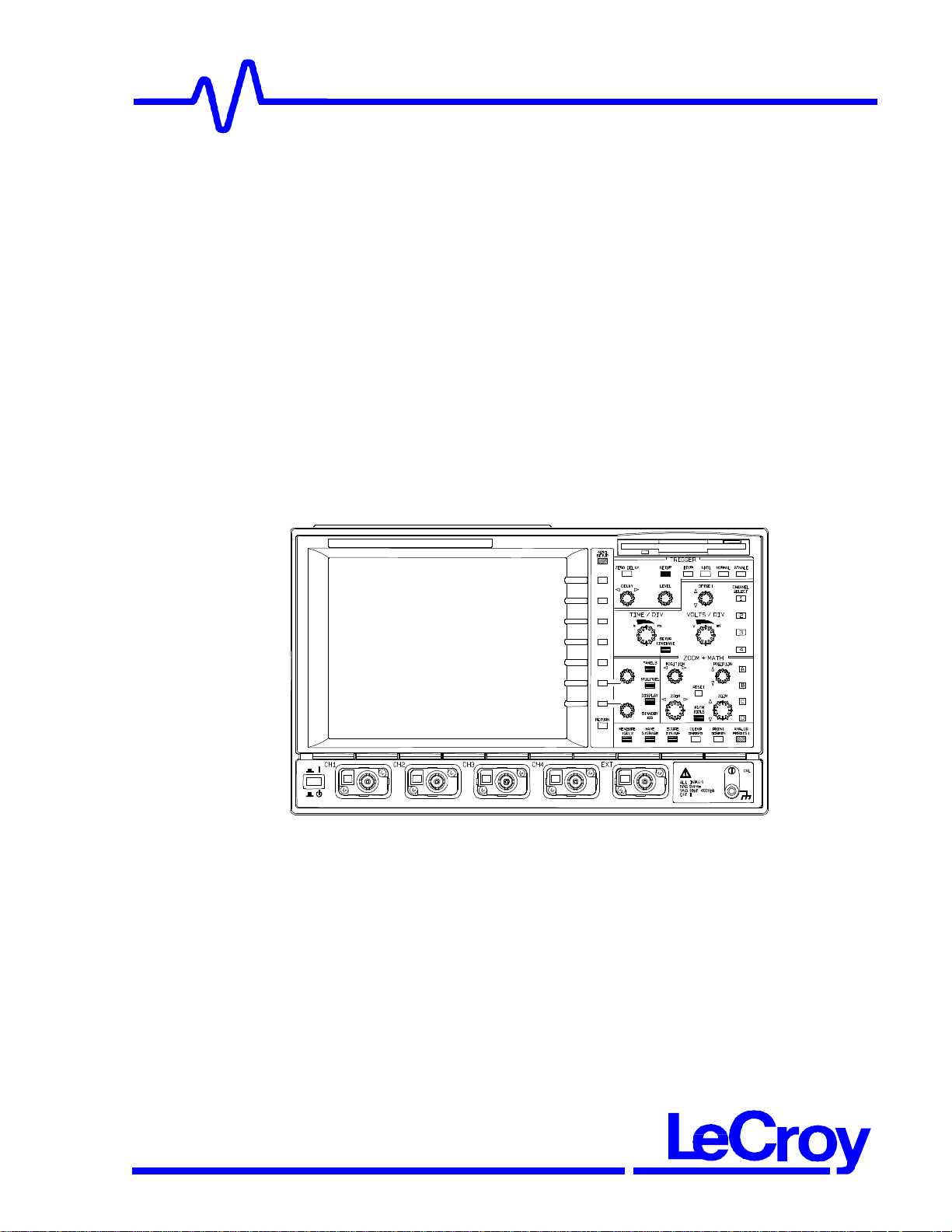
Page 1
LeCroy waverunner
LT Series
Service Manual
Version A- October 1999
Page 2

LeCroy Corporate Headquarters
700 Chestnut Ridge Road
Chestnut Ridge, NY 10977-6499
USA
Tel : (914) 425-2000
Fax : (914) 425-8967
http://www.lecroy.com
Copyright © October 1999. LeCroy is a registered trade-mark of LeCroy Corporation.
All rights reserved. Information in this publication supersedes all earlier versions.
Specifications subject to change.
Page 3

Read this First
1. Warranty and Product Support
Note: This warranty replaces all other warranties, expressed or implied, including but
particular purpose or use. LeCroy shall not be liable for any special, incidental, or
for the transportation and insurance charges for the return of products to the service
facility. LeCroy will return all products under warranty with
It is recommended that you thoroughly inspect the contents of the oscilloscope
packaging immediately upon receipt. Check all contents against the packing
list/invoice copy shipped with the instrument. Unless LeCroy is notified promptly of
any missing or damaged item, responsibility for its replacement cannot be
accepted. Contact your nearest LeCroy Customer Service Center or national
distributor immediately (see chapter 2 for contact numbers).
1.1 Warranty
LeCroy warrants its oscilloscope products for normal use and operation within
specifications for a period of three years from the date of shipment. Calibration
each year is recommended to ensure in-spec. performance. Spares, replacement
parts and repairs are warranted for 90 days. The instrument's firmware has been
thoroughly tested and is thought to be functional, but is supplied without warranty
of any kind covering detailed performance. Products not made by LeCroy are
covered solely by the warranty of the original equipment manufacturer.
Under the LeCroy warranty, LeCroy will repair or, at its option, replace any product
returned within the warranty period to a LeCroy authorized service center.
However, this will be done only if the product is determined after examination by
LeCroy to be defective due to workmanship or materials, and not to have been
caused by misuse, neglect or accident, or by abnormal conditions or operation.
1.2 Product Assistance
not limited to any implied warranty of merchantability, fitness, or adequacy for any
consequential damages, whether in contract or otherwise. The client will be responsible
Help on installation, calibration, and the use of LeCroy equipment is available from
the LeCroy Customer Service Center in your country.
1.3 Maintenance Agreements
LeCroy provides a variety of customer support services under Maintenance
Agreements. Such agreements give extended warranty and allow clients to budget
maintenance costs after the initial three-year warranty has expired. Other services
such as installation, training, enhancements and on-site repairs are available
through special supplemental support agreements.
1.4 Staying Up to Date
LeCroy is dedicated to offering state-of-the-art instruments, by continually refining
and improving the performance of LeCroy products. Because of the speed with
which physical modifications may be implemented, this manual and related
documentation may not agree in every detail with the products they describe. For
transport prepaid.
Read this First 1-1
Page 4

example, there might be small discrepancies in the values of components affecting
pulse shape, timing or offset, and — infrequently — minor logic changes. However,
be assured the scope itself is in full order and incorporates the most up-to-date
circuitry. LeCroy frequently updates firmware and software during servicing to
improve scope performance, free of charge during warranty. You will be kept
informed of such changes, through new or revised manuals and other publications.
Nevertheless, you should retain this, the original manual, for future reference
to your scope’s unchanged hardware specifications.
1.5 Service and Repair
Please return products requiring maintenance to the Customer Service Department
in your country or to an authorized service facility. The customer is responsible for
transportation charges to the factory, whereas all in-warranty products will be
returned to you with transportation prepaid. Outside the warranty period, you will
need to provide us with a purchase order number before we can repair your LeCroy
product. You will be billed for parts and labor related to the repair work, and for
shipping.
1.6 How to return a Product
Contact the nearest LeCroy Service Center or office to find out where to return the
product. All returned products should be identified by model and serial number.
You should describe the defect or failure, and provide your name and contact
number. In the case of a product returned to the factory, a Return Authorization
Number (RAN) should be used.
Return shipments should be made prepaid. We cannot accept COD (Cash On
Delivery) or Collect Return shipments. We recommend air-freighting.
It is important that the RAN be clearly shown on the outside of the shipping
package for prompt redirection to the appropriate LeCroy department.
1.7 What Comes with Your Scope
The following items are shipped together with the standard configuration of this
oscilloscope:
• Front Scope Cover
• 10:1 10 MΩ PP006 Passive Probe — one per channel
• Two 250 V Fuses, AC Power Cord and Plug
• Operator’s Manual , Remote Control Manual, Hands-On Guide
• Performance Certificate or Calibration Certificate, Declaration of Conformity
Note: Wherever possible, please use the original shipping carton. If a substitute
carton is used, it should be rigid and packed so that that the product is surrounded
by a minimum of four inches or 10 cm of shock-absorbent material.
1-2 Read this First
minimum of four inches or 10 cm of shock-absorbent material.
Page 5

2. General Information
2.1 Product Assistance
Help on installation, calibration, and the use of LeCroy equipment is available from your
local LeCroy office, or from LeCroy’s
• Customer Care Center, 700 Chestnut Ridge Road, Chestnut Ridge,
New York 10977–6499, U.S.A., tel. (914) 578–6020
• European Service Center, 2, rue du Pré-de-la-Fontaine, 1217 Meyrin 1, Geneva
Switzerland, tel. (41) 22/719 21 11.
• LeCroy Japan Corporation, Sasazuka Center Bldg – 6th floor, 1-6, 2-Chome,
Sasazuka, Shibuya-ku, Tokyo Japan 151-0073, tel. (81) 3 3376 9400
2.2 Installation for Safe and Efficient Operation
Operating Environment
For safe operation of the instrument to its specifications, ensure that the operating
environment is maintained within the following parameters:
Temperature............. 5 to 40 °C (41 to 104 °F) rated.
Humidity....................Maximum relative humidity 80 % RH (non-condensing) for
temperatures up to 31 °C decreasing linearly to 50 % relative
humidity at 40 °C
Altitude......................< 2000 m (6560 ft)
The oscilloscope has been qualified to the following EN61010-1 category:
Installation (Overvoltage) Category ........................ II
Protection Class......................... …........................I
Pollution Degree........................ ............................2
General Information 2-1
Page 6
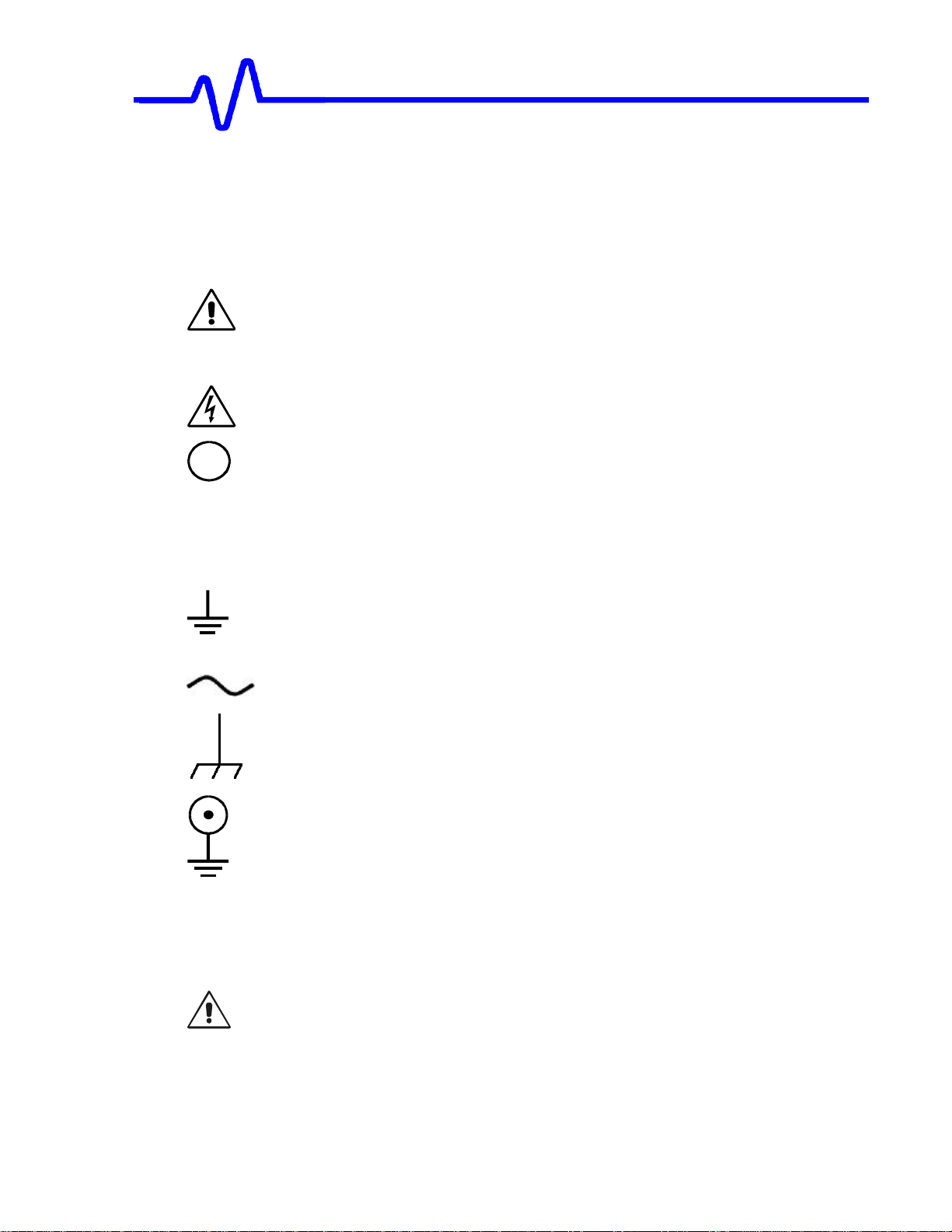
Safety Symbols
Where the following symbols or indications appear on the instrument’s front or rear
panels, or elsewhere in this manual, they alert the user to an aspect of safety.
..........................CAUTION: Refer to accompanying documents (for Safety-
related information). See elsewhere in this manual wherever
the symbol is present.
..........................CAUTION: Risk of electric shock
...........................On (Supply)
x...................................Standby (Supply)
............................Earth (Ground) Terminal
...................... Alternating Current Only
........................ Chassis Terminal
............................Earth (Ground) Terminal on BNC Connectors
WARNING.................Denotes a hazard. If a WARNING is indicated on the
instrument do not proceed until its conditions are
understood and met.
WARNING
Any use of this instrument in a manner not specified by the manufacturer
may impair the instrument’s safety protection.
2-2 General Information
Page 7

The oscilloscope has not been designed to make direct measurements on the
human body. Users who connect a LeCroy oscilloscope directly to a person do so
at their own risk. Use only indoors.
Power Requirements
The oscilloscope operates from a 100 V to 240V AC power source at 50 Hz to
60 Hz.
No voltage selection is required, since the instrument automatically adapts to the
line voltage present.
Fuses
The power supply of the oscilloscope is protected against short-circuit and overload
by means of two 6.3 A/250 V AC “T”-rated fuses, located above the mains plug.
Disconnect the power cord before inspecting or replacing a fuse. Open the fuse
box by inserting a small screwdriver under the plastic cover and prying it open. For
continued fire protection at all line voltages, replace only with fuses of the specified
type and rating (see above).
Ground
The oscilloscope has been designed to operate from a single-phase power source,
with one of the current-carrying conductors (neutral conductor) at ground (earth)
potential. Maintain the ground line to avoid an electric shock.
None of the current-carrying conductors may exceed 250 V rms with respect to
ground potential. The oscilloscope is provided with a three-wire electrical cord
containing a three-terminal polarized plug for mains voltage and safety ground
connection. The plug's ground terminal is connected directly to the frame of the
unit. For adequate protection against electrical hazard, this plug must be inserted
into a mating outlet containing a safety ground contact.
Cleaning and Maintenance
Maintenance and repairs should be carried out exclusively by a LeCroy technician.
Cleaning should be limited to the exterior of the instrument only, using a damp, soft
cloth. Do not use chemicals or abrasive elements. Under no circumstances should
moisture be allowed to penetrate the disk drive analyzer. To avoid electric shocks,
disconnect the instrument from the power supply before cleaning.
CAUTION
Risk of electrical shock: No user-serviceable parts inside. Leave repair to
qualified personnel.
General Information 2-3
Page 8

Power On
Connect the oscilloscope to the power outlet and switch it on using the power
On/Standby button, located near the left-hand corner of the instrument below the
screen. After the instrument is switched on, auto-calibration is performed and a test
of the disk drive analyzer's ADCs and memories is carried out. The full testing
procedure takes approximately 10 seconds, after which time a display will appear
on the screen.
2-4 General Information
Page 9

Specifications
3. Instrument Architecture Overview
PROCESSORS
The Waverunner central processor (CPU), a PowerPC microprocessor, performs
the oscilloscope’s computations and controls its operation. A range of peripheral
interfaces allow you to control remotely, store waveforms and other data, and make
hard copies. A support processor constantly monitors the front-panel controls.
Waverunner either transfers data to display memory for direct waveform display, or
stores it to reference memories, for fast data-processing.
ADCs
Each Waverunner channel has an eight-bit Analog-to-Digital Converter (ADC). The
instrument’s ADC architecture is designed to give excellent amplitude and phase
correlation, maximum analog-to-digital conversion performance, large record
lengths and superior time resolution.
MEMORIES
Waverunner acquisition memories simplify signal acquisition by producing
waveform records that allow detailed analysis over large time intervals. There are
four memories for temporary storage, and four more for waveform zooming and
processing.
RIS
The Waverunner oscilloscope captures and stores repetitive signals at a maximum
Random Interleaved Sampling (RIS) rate of 25 GS/s. This advanced digitizing
technique enables measurement of repetitive signals with an effective sampling
interval of 40 ps, and a measurement resolution of up to 5 ps.
TRIGGER SYSTEM
You can control Waverunner triggering to a highly specialized degree in
accordance with waveform characteristics and chosen trigger conditions. The
trigger source can be any of the input channels, line (synchronized to scope’s main
input supply) or external. The coupling is selected from AC, LF REJect, HF REJect,
HF, and DC; the slope from positive and negative. Waverunner SMART Trigger
offers a wide range of sophisticated trigger modes matched to special trigger
conditions and sets of conditions.
AUTOMATIC CALIBRATION
Waverunner automatic calibration ensures an overall vertical accuracy of typically 1
% of full scale. Vertical gain and offset calibration, and horizontal (time) resolution
take place each time you change the volts per division setting. Periodic and
temperature-dependent auto-calibration ensures long-term stability at the current
setting.
Specifications 3-1
Page 10

DISPLAY SYSTEM
You control the display’s interactive, user-friendly interface using push-buttons and
knobs. Display as many as eight different waveforms at once on eight separate
grids. The parameters controlling signal capture are simultaneously reported. The
Waverunner display presents internal status and measurement results, as well as
operational, measurement, and waveform-analysis menus.
The 8.4-inch color flat-panel TFT-LCD screen presents waveforms and data using
advanced color management. Overlap-mixing and contrast-enhancement functions
ensure that overlapping waveforms remain distinct at all times. Both pre-set and
personal color schemes are available.
The Analog Persistence function offers display attributes of an analog instrument
with all the advantages of digital technology. The Full Screen function expands
waveform grids to fill the entire screen.
A hard copy of the screen can be easily produced by pressing the front-panel
PRINT SCREEN button.
INTERFACE AND PANEL SETUPS
Although Waverunner is a truly digital instrument, the front-panel layout and
controls are similar to an analog oscilloscope’s. Rapid response and instant
representation of waveforms on the high-resolution screen add to this impression.
Four front-panel setups can be stored internally and recalled either directly or by
remote control, thus ensuring rapid front-panel configuration. When power is
switched off, the current front-panel settings are automatically stored for
subsequent recall at the next power-on.
REMOTE CONTROL
Waverunner has also been designed for remote control operation in automated
testing and computer-aided measurement applications. You control the entire
measurement process — including cursor and pulse-parameter settings, dynamic
modification of front-panel settings, and display organization — through the rearpanel industry-standard GPIB (IEEE-488) and standard RS-232-C ports. See this
manual’s Chapter 12, Use Waverunner with PC, and the Remote Control Manual.
3-2 Specifications
Page 11
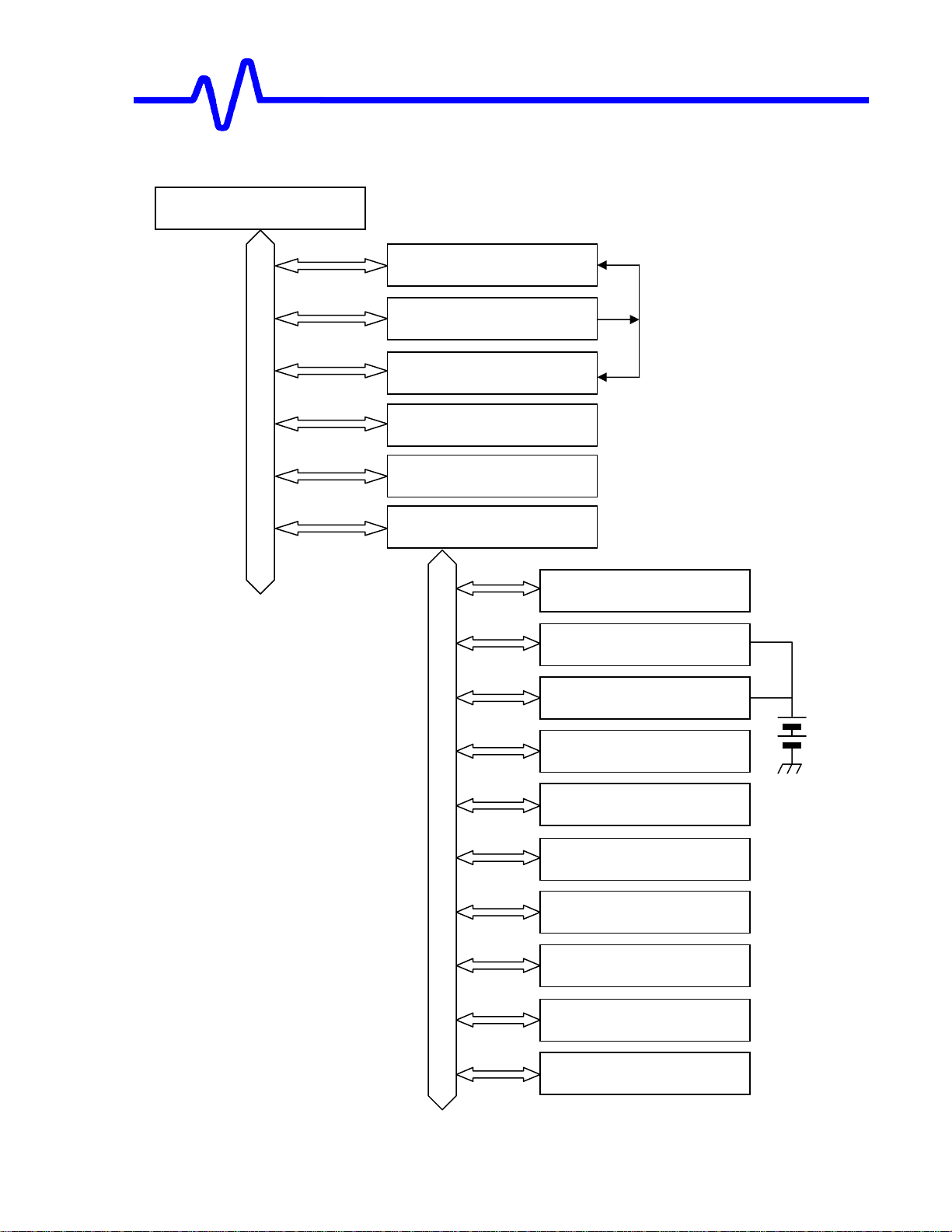
Display
Processor
CH1
Program Memory
Microprocessor
with Integrated
Fast
memory
memory
Optional Storage
BLOCK DIAGRAM: Hi-Z, 50 W Amplifiers + Attenuators
CH2
External
Trigger
Sample
& Hold
Sample
& Hold
Trigger
Logic
8-Bit ADC(s)
8-Bit ADC(s)
Timebase
Fast
memory
Fast
memory
Devices
Floppy Disk
Interface
Centronics
RS-232-C
GPIB
Power PC
CH3
CH4
Sample
& Hold
Sample
& Hold
8-Bit ADC(s)
8-Bit ADC(s)
Fast
Cache Memory
Front-Panel
Processor
Real-Time
Clock
Data Memories
Specifications 3-3
Page 12
Specifications
MODELS
Waverunner LT342/322 Series: Two channels
Waverunner LT344 Series: Four channels
ACQUISITION SYSTEM
Bandwidth (−3dB): LT342/LT344/LT322:500 MHz;LT224:200 MHz @ 50 Ω and at probe
tip with PP006
Bandwidth Limiter at 25 MHz and 200 MHz can be selected for each channel LT224 is
25MHz.
Input Impedance: 50 Ω ± 1.0 %; 1 MΩ ± 1.0 % // 16 pF typical
Input Coupling: 1 MΩ: AC, DC, GND; 50 Ω: DC, GND
Max Input: 50 Ω: 5 Vrms; 1 MΩ: 400 V max (peak AC <-5 kHz + DC)
Single Shot Sampling Rate: 500 MS/s
Acquisition Memory: LT342/LT344;250 000 points per channel; 1 M points per channel
on L modelsLT224/LT322; 100 000
Vertical Resolution: 8 bits
Sensitivity: 2 mV–10 V/div
Offset Range:
Ø 2 mV–99 mV/div: ± 1 V
Ø 100 mV–0.99 mV/div: ± 10 V
Ø 1 V–10 V/div: ± 100 V
ACQUISITION MODES
MODE TIME BASE SETTING MAXIMUM RATE DESCRIPTION
Single Shot
LT342(L)/LT344(L) 10 ns to 1000 s/div 500 MS/s
One ADC per channel
LT224/LT322 20 ns to 1000 s/div 200 MS/s
Repetitive
LT342(L)/LT344(L)
LT224/LT322
1 ns to 5 µsec/div
1 ns to 10 µsec/div
25 GS/s
10 GS/s
Random Interleaved
Sampling (RIS)
Sequence Mode
3-4 Specifications
Page 13

LT342/LT344 2–1000 segments 500 MS/s
Stores Multiple Events
with time stamp in
segmented acquisition
memories
LT224/LT322 2–400 segments 200 MS/s
Stores Multiple Events
with time stamp in
segmented acquisition
LT342L/LT344L 2–4000 segments 500 MS/s
≤ 500 000 pts:
Roll Mode
500 ms–1000s/div
≥ 500 000 pts:
100 ks/s
1 s–1000s/div
memories
Waveform slowly rolls
across display when
used with slow time
bases.
TIMEBASE SYSTEM
Timebases: Main and up to four zoom traces simultaneously
Time/Div Range: 1 ns/div to 1000 s/div
Clock Accuracy: ≤ 10 ppm
Interpolator Resolution: 5 ps
External Clock: ≤ 500 MHz, 50 Ω, or 1 MΩ impedance
TRIGGERING SYSTEM
Modes: NORMAL, AUTO, SINGLE and STOP
Sources: Any input channel, External, EXT 10 or line; slope, level and coupling are
unique to each source (except line trigger)
Coupling Modes: DC(DC to 250MHz/LT224; DC to 200MHz), AC(Applox.7.5Hz to
250MHz/LT224; Approx.7.5Hz to 200MHz), HF(to 500MHz/LT224 not have), HFREJ,
LFREJ (reject frequency 50 kHz typical)
Pre-Trigger Recording: 0–100 % of horizontal time scale
Post Trigger Delay: 0–10 000 divisions
Holdoff by Time or Events: Up to 20 s or from 1 to 99 999 999 events
Internal Trigger Range: ± 5 div
Maximum Trigger Frequency: Up to 500 MHz with HF coupling
External Trigger Input: ± 0.5 V, ± 5 V with Ext 10; max input same as input channels
SMART TRIGGER TYPES
Signal or pulse width: Triggers on glitches down to 2 ns(LT224 is 3ns). Pulse widths are
selectable between < 2.5 ns to 20 s.
Signal interval: Triggers on intervals selectable between 10 ns and 20 s.
Specifications 3-5
Page 14

TV: Triggers on line (up to 1500) and field 1 or 2 (odd or even) for PAL (SECAM), NTSC,
or non-standard video.
State/Edge qualified: Triggers on any input source only if a given state (or transition) has
occurred on another source. Delay between sources is selectable by time or number of
events.
Dropout: Triggers if the input signal drops out for longer than a selected time out between
25 ns and 20 s.
AUTOSETUP
Automatically sets timebase, trigger, and sensitivity to display a wide range of repetitive
signals.
Vertical Find: Automatically sets sensitivity for the selected input signal
PROBES
Model PP006: PP006 with auto-detect: 10:1, 10 MΩ; one probe per channel
Probe System: ProBus Intelligent Probe System supports active, high-voltage, current,
and differential probes, and differential amplifiers
COLOR WAVEFORM DISPLAY
Type: Color 8.4-inch flat-panel TFT-LCD with VGA, 640 x 480 resolution
Screen Saver: Display blanks after 10 minutes
Real Time Clock: Date, hours, minutes, and seconds displayed with waveform
Number of Traces: Maximum eight on LT344/LT224 Series, six on LT342/LT322 Series;
simultaneously display channel, zoom, memory, and math traces
Grid Styles: Single, Dual, Quad, Octal, XY, Single+XY, Dual+XY; Full Screen gives
enlarged view of each style
Waveform Display Styles: Sample dots joined or dots only — regular or bold
ANALOG PERSISTENCE DISPLAY
Analog Persistence and Color Graded Persistence: Variable saturation levels; stores
each trace’s persistence data in memory
Trace Display: Opaque or transparent overlap
ZOOM EXPANSION TRACES
Style: Display up to four zoom traces
Vertical Zoom: Up to 5x expansion, 50x with averaging
Horizontal Zoom: Expand to 2 pts/div, magnify to 50 000x
Autoscroll: Automatically scan and display a captured signal
RAPID SIGNAL PROCESSING
Processor: Power PC 603e
3-6 Specifications
TM
Page 15

LT342/LT322 LT344/LT224 LT342L LT344L
2.1.1 16 Mbytes 2.1.2 16 Mbytes 2.1.3 32 Mbytes 2.1.4 32 Mbytes
64 MBYTE SYSTEM MEMORY OPTIONAL FOR ALL MODELS
INTERNAL WAVEFORM MEMORY
Waveform: M1, M2, M3, M4; memory length equal to acquisition memory
Zoom and Math: A, B, C, D; memory length equal to acquisition memory
Memories M1–4 and A–D store full-length waveforms with 16 bits/data point
SETUP STORAGE
For front panel and instrument status: Four non-volatile memories and floppy drive are
standard; hard drive and memory card are optional
MATH TOOLS
Simultaneously perform up to four math processing functions; traces can be chained
together to perform math on math. Standard functions: add, subtract, multiply, divide,
negate, identity, summation, averaging to 1000 sweeps, ERES low-pass digital filters for
11-bit vertical resolution, FFT of 50 kpoint waveforms, Extrema for displaying envelope
roof and floor, physical units, rescale (with units), sin x/x, resample (deskew).
MEASURE TOOLS
Cursor Measurements:
Ø Relative Time: Two arrow-style cursors measure time and voltage differences relative
to each other with a resolution of ± 0.05 % full scale.
Ø Relative Amplitude (Voltage): Two horizontal bars measure voltage differences at
± 0.2 % fs resolution.
Ø Absolute Time: Cross-hair marker measures time relative to trigger and voltage with
respect to ground.
Ø Absolute Amplitude (Voltage): A horizontal reference line cursor measures voltage
with respect to ground.
Automated Measurements: Display any five parameters together with their average, high,
low and standard deviations.
Pass/Fail: Test any five parameters against selectable thresholds. Limit testing is
performed using masks created on the scope or on a PC. Setup a pass or fail condition to
initiate actions such as hardcopy output, save waveform to memory, GPIB SRQ, or pulse
out.
EXTENDED MATH AND MEASUREMENTS OPTION
Adds math and advanced measurements for general-purpose applications. Math Tools is
expanded to include all standard math plus integration, derivative, log and exponential
(base e and base 10), square, square root, absolute value, plus data log when using the
trend function.
Specifications 3-7
Page 16

WAVEANALYZER OPTION
Adds math processing to include FFTs of 1 Mpoint waveforms, power spectrum density,
spectrum averaging, waveform averaging to one million sweeps, continuous averaging,
waveform histograms, and histogram parameters. Includes the Extended Math and
Measurement option.
SPECIAL APPLICATION SOLUTIONS
Jitter and Timing Analysis (JTA): Precision cycle-to-cycle timing measurements with
enhanced accuracy, histograms on persistence traces, persistence to waveform tracing
and full statistical analysis.
PowerMeasure: A complete solution for the power conversion engineer. Includes timing
deskew of voltage and current, and rescale to electrical units.
INTERFACE
Remote Control: Full control via GPIB and RS-232-C
Floppy Drive: Internal, DOS-format, 3.5" high-density
PC Card Slot: Supports memory and hard drive cards
External Monitor Port: 15-pin D-Type VGA-compatible
Centronics Port: Parallel printer interface
Internal graphics printer (optional): 25 mm/s max, 112 mm paper width; provides
hardcopy output in <10 seconds
OUTPUTS
Calibrator signal: 500 Hz–1 MHz square wave, −1.0 to +1.0, test point, and ground lug on
front panel
Control signals: Choice of trigger ready, trigger out, or Pass/Fail status; TTL levels into 1
MΩ at rear panel BNC (output resistance 300 Ω ± 10 %)
GENERAL
Operating Conditions: Temperature 5–40° C; humidity 80 % non-condensing at 40° C;
altitude ≤ 2000 m
Shock and Vibration: Conforms to MIL-PRF-28800P; Class C
Power Requirements: 90–132 V AC and 180–250 V AC; 45–66 Hz; maximum power
dissipation 150 VA–230 VA, depending on model
Certifications: CE, UL and cUL
Dimensions (HWD): 210 mm x 350 mm x 300 mm (8.3" x 13.8" x 11.8"); height excludes
scope feet
Weight: 8 kg (18 lbs)
Warranty and Calibration: Three years; calibration recommended yearly
3-8 Specifications
Page 17

4. Theory of Operation
4.1 Processor Board
MPC603e Processor
The PowerPC603e on the processor board is a 4-bit RISC processor having
2x32Kbyte cache and features high speed processing and quick memory access.
The processor is designed to operate with an internal clock which is several times
the external bus clock cycles and is used under the 32bit mode.
The board consists of two circuit-blocks:
• The 32bit block, that contains the main PowerPC processor, dynamic RAM
modules, VGA interface, Super-I/O and main board interface.
• The 8bit block, which incorporates all peripher als and other interfaces for outer
connections.
These two circuit-blocks are connected thr ough MC68150 (dynamic bus sizer).
Power Supply
The board requires two power sources (Vcc and +12V). +12V source is used for
OP-amp and small-peripheral operation.
The processor requires 3.3V, and all other logic devices are operated by the +5V
source. All of the signals are TTL compatible.
The processor allows +5V input signals and does not require logic level conversion.
An OP-amp and MOSFET transistor consist of 3.3V power source. The r eference
voltage is taken through the voltage-resistor divider network across +5V power
source.
32bit Peripherals
There are six devices hooked on the processor’s 32bit data bus:
• VGA video contr oller
• DRAM system
• bus sizer, an int er face to 8bit circuit-block
• DMA controller
• Super-I/O
• MAIN board
Theory of Operation
Theory of Operation 4-1
Page 18
CPU’s Block Diagram
CPU:PowerPC 603e
DRAM:2X128MB max
DMAC:71071
Super I/O
RS232C, Parallel, Floppy Disk
MAIN Board I/F
VGA:65545
BUS Sizer:MC68150
32bit BUS
Flash PROM: 2MBmax
NVRAM:128KB
Real Time Clock
Interrupt Controller
Front Panel I/F
GP-IB
Internal Printer I/F
Small Peripherals
PCMCIA type I/II/III
4-2 Theory of Operation
Other Control Ports
8bit BUS
Page 19

DRAM
The DRAM circuit consists of one or two SIMM modules, const ituting f rom 16MB to
a maximum of 128 MB. The SIMM modules to be supported are only of EDO types.
The DRAM control circuit is built with one piece each of CPLD and GAL, and
several gate ICs.
The DRAMC (IC13) located on the main control circuit, generat es all types of bus
cycle timing(normal R/W, 2-beat/8-beat bursts of R/W), refresh cycles, and DMA
cycles. It also generates signals f or automatic incr ement of column- addresses to be
used in burst transfer mode. Furthermore, the DRAMC has a register f or set ting one
or two SIMMs and determining SIMM size (whether it is less than 32MB or more
than 64MB), in order to adjust the memory mapping so as not to have gaps in
memory mapping according with the memory capacity.
The CAS (IC14) distributes signals for column address selection t o the CAS signal
circuits of each SIMM chip. CAS is selected by the size of memory access (1, 2, 3,
and 4 bytes), accessing start-address, and type of bus cycles (normal, burst,
refresh and DMA).
Two multiplexers (IC9 and IC10) switch the address lines of odd and even
addresses to be connected with the address lines of each SIMM. The other
multiplexer (IC11) switches low order address bits, i.e. , routing them either directly
to the processor or to the low order address generated in DRAMC.
Normal Access Timing
This is the simplest access possible: the processor puts an address onto the
address bus and reads or writes the required data out of or to the DRAM which
corresponds with the bus.
The bus width is 32bits, or 4bytes wide, and the CPU performs to read or write
operations (of one through four bytes) which are chained in a bus cycle.
Burst Access Timing
A burst access, on the 603e configured with 32bit device operation, performs either
two or eight successive reads in DRAM (2-beat or 8-beat burst access). The idea is
to put the beginning of an addr ess onto the address bus and read/write data out of
or to DRAM every clock cycle, without incrementing the address required by the
processor (this is to be achieved by the external logic circuit). Using EDO-DRAM
enables to read and write every 30ns of clocks similarly as with one or two SI MMs.
The 8-beat access is indicated by an active “low” of NTBST signals and a 32bit
access signal (SIZ2..0=011), and the 2-beat access is indicated by an active “high”
of NTBST signals and an access size of 64 bit s ( SI Z2. .0=100).
Refresh Timing
The 32 KHz clock from the RTC chip is used to generate the timing to refresh
DRAM. Without this clock , the DRAM would not be refreshed and all the dat a in it
would be erased out. DRAMC detects the rising edge and the falling edge of t his
32KHz clock. At the each edge, it generates the CAS before RAS refreshes the
cycles.
The arbitration logics between other accesses (bus cycle with the processor and
DMA cycle) and refresh cycles reside in the DRAMC.
DMA Timing
The DMA access can be used for data transfer t o and from floppy disks.
Theory of Operation 4-3
Page 20

The data is transferred in between the I/O and DRAMs by simultaneously accessing
the desired addresses in the Super I/O and DRAMs.
The addresses A0 to A25 (as well as lower addresses up to 64MB on the memory
map) can be accessed through the DMA controller. Since the Super I/O is directly
connected to its 8bit to 32bit bus without passing through the bus sizer, data
transfer can be done only to and from m em or y areas in which addresses are divided
by intervals of 4bytes each.
Memory Mapping
When the main switch is on, the internal sof tware automatically sets the system’s
memory size to the largest capacity available with the SIMM mounted (2 pieces of
128 MB SIMM size). It also checks whether all the addresses are perennial or not t o
prevent having "holes" in the address space. Through this operation, available
memory capacity in the SIMM mounted is correctly judged and the capacity
information is stored again int o the DRAMC register. Thus, all the address spaces
are assured for perennial address continuation.
VGA controller
The VGA controller chip 65545(IC29) contains t he logic circuits to decode its own
addresses. It generates all the video signals (RGB, H/V, and all contro l lines to drive
the flat panel), and controls its associated 1 MB video DRAM (to read, write and
refresh).
The total of video DRAMs mounted are two pieces of 2MB (but 512KB each of the
DRAM only are used).
All timings are extracted from the 16MHz bus clock; theref ore, no external crystal or
time-base is required. The hor izontal and vert ical synchronization sig nals ar e sent to
the external video connector (a half pitch, D-SUB15 pin connector is used).
The 65545 chip can support several bus interfaces (PCI, ISA, VL, etc) , the system
employs it for VL-bus applications with the mode of 256-color palette operations.
The controller has an 18bit color palette and can display 256 colors out of the
available 260,000. However, the liquid crystal panel can only use 12-bit color data,
and color display is limited to 256 out of 4,096 colors (the color data will be
extended to 18bits in the future).
The power supply circuit for the liquid crystal panel has a MOSFET switch that t urns
the power for the LCD with the reset signal, since the LCD needs to minimize its
start-up time.
Super-I/O
This device controls RS-232Cs, floppy disks, and parallel port operations. The
controller has its own time-base with a 24MHz crystal. RS-232C can be used by
simply connecting the MAX232 buffer (IC31) to it. Since the Super I/O chip has a
16-byte buffer, hig h speed data transfer is easily carried out.
A 2HD disk drive can be directly connected to the system without any external
components other than a piece of pull-up resistor; it can be operated in either
interruption mode or DMA mode.
The parallel interface is also activated without ot her external component s ot her than
a piece of pull-up resistor, for the use of 2-way communication.
This IC chip has an IDE interface f unction in it, but this boar d does not support the
function.
4-4 Theory of Operation
Page 21

Bus Control
The DEC32 (IC17) perfor ms decoding operat ions for the circuits (32bit circuit block)
which are directly connected to the processor (except the DRAM).( The DRAMC
performs decoding operat ions for the DRAMs).
The RW32 (IC76) generates the control signals of read/write for the devices
associated with the DMA, and the byte enable signals (NBE0-3) for the VGA
controller.
When the bus cycle start s, 603e must terminate the bus cycle by returning signals
after acknowledging each of the data and addresses, f rom the outside. The ACK32
(IC19) is used to generate the acknowledgement signals.
The ARBT (IC18) has logics for arbitration between the DMA and processor
accessing, and performs for ced ter mination of t he bus operat ion when the bus cycle
can not be finished within a defined time.
The ACK8 (IC21) has logics for generation of the acknowledgement signals and
read write strobe signals in the 8bit peripheral cir cuit block.
The DEC8 (IC22) has logics for decoding 8bit peripheral circuits, and a certain
circuit involved in the address latch operation.
Bus Sizer
The MPC603e processor does not support dynamic bus sizing, which is perf ormed
with the 68K processor family. Each 8bit of a 32bit bus is f ixed or assig ned with the
lower addresses, or 0 through 3 bits. Therefore, if an 8bit device were directly
connected to the bus, this device would be seen in 4byte steps each in the memory
map area. To avoid this, the 8bit-bus per ipheral unit shall be connected to t he 32bit bus through the bus sizer, MC68150 (IC15). The bus sizer divides one bus cycle for
accessing 32 bit-bus of the processor into four cycles each of 8bit accessing cycle,
and/or assigns 8bit-bus data to a corr esponding 8bits within the 32bits.
8bit Peripherals
The following devices are listed as 8bit data bus units:
• PCMCIA Interface
• Flash PROM
• NVRAM
• RTC
• Interrupt Controller
• GPIB Interface
• Small-peripherals Interface
• Internal printer Interface
• Front-Panel I/F
• Ot her r egisters and ports
PCMCIA, type I/II/III interface
This interface consists mainly of buffers for bot h dat a and addr ess busses.
The CARD (IC71) generates the control signals both for memory card mode and I/O
card mode.
The IC65 (D-F/F) holds control bits for the signals resetting the card, switching
between the data area and the attribute area, and switching the card’s modes. All
bits in the register are reset to zero when the _RESET signal goes to active low,
Theory of Operation 4-5
Page 22

which means that their state is also guaranteed at power-up.
The IC66 and the IC67 invert the most signif icant address bits of the memory card
whenever the SWAP jumper is plugged in, so that the first bytes are always
allocated to “FFF00000”, regardless of the size of the memory card. This allows to
boot directly from the PCMCIA memory card used.
Flash PROM
Two pieces of the Intel’s 29F008-compatible 1MB PROMs (IC45 and 46) are used
to operate in the 8-bit bus mode. These ICs do not require any programming
voltage to write.
From a hardware point of view, a flash PROM is regarded the same as an EPROM
in read mode.
To erase or write to memory, commands ar e written into the data bus. Writ ing and
erasing must be performed over monitoring the stat us-signals (RY/#BY) on the por t
(IC49).
The program may be seen to start from the Flash PROM. The Flash PROM is,
however, not regarded as the program or its program area even when start-up
(even when the screen appears) is completed, because the program must be
processed in the DRAM after transferring the program content from the Flash
PROM into the DRAM.
NVRAM
This memory chip is powered from the VCCO in the RTC. W hen the main power is
set to off, the required power for the NVRAM is fed through the lithium battery
installed. W hen t he power is set to on, it is powered from the VCC.
The #CS1 signals are also controlled through the RTC. When the main power is set
to off, the RT C sets the chip select to the “high” level through a pull-up resistor to
place the SRAM a power-down mode to prevent any accidental overwriting.
RTC
The DS1689 real time clock has several funct ions:
• Keeping t he time-of-day and current-date information while power is off.
• Gener ating 32KHz clock for DRAM refreshm ent.
• Giving 128Hz of periodic interrupt signals to force bus accessing from the
processor and allowing periodic updating of the t ime display.
• Providing a unique ID that identifies the or igination of scope ID.
• Feeding t he power and the chip select signal to the NVRAM.
The chip generates timing clocks necessary for time k eeping and driving all other
circuits by connecting to 32.768KHz crystal. A few discrete components around it
leave the chip powered, when the system is set to off, by the backup lit hium battery
while the rest of the board is not powered, and charge t he battery when the power is
on again.
Accesses from the processor are done through the cir cuit f or the bus separat ion, f or
addresses and data are multiplexed.
The unique ID was already written in the RTC by the manufacturer, since every
different value must be stor ed in each chip.
Interrupt Controller
4-6 Theory of Operation
Page 23

In order to prioritize and control several interrupt sources, it is necessary to use an
IC of uPD71059. It scans eight int errupt signals and sends a uniq ue interr upt signal
to the processor when an (unmasked) interrupt signal appears.
Interrupt levels are assigned as follows:
level 0 (lowest priority) FDC
level 1 small peripherals
level 2 RS232C
level 3 GP-IB
level 4 PCMCIA(I/O card mode)
level 5 real time clock
level 6 the MAIN board
level 7 (highest priority) unused
The priority in the above can be changed by the software.
Small Peripheral Interface
This 8-bit interface is int ended t o allow external expansion of t he boar d in addition to
the processor board.
The tri-state buffers drive the address and control lines, and bi-directional buffers
drive data lines.
The address decoding is processed on each expanded peripheral board. Since the
acknowledgement toward each access is also returned by the expanded board,
there is no restriction to the amount of wait-states.
The bus clock runs at 16MHz, and a reset line reinitializes the boards as does in the
CPU.
Four interrupt lines are also included in this interface, so that interr upt-dr iven boards
can be used.
Front Panel
The front panel is accessed by serial read/write signals passing through the IC47
and IC48.
The CPU board can be reset by resetting the 3 buttons on the front panel. This
function becomes eff ect ive by setting a bit of IC52 for enabling.
Both LED and BEEP are activated by serial writing. LED and BEEP are initialized off
by the resetting operation.
Theory of Operation 4-7
Page 24

Reset Circuit
The power supply is monitored by the IC4 chip. Whenever the Vcc goes below 4.5V
(even for a very short time), a reset pulse, in which the width is determined by the
C6’s capacity, is generated.
Resetting 3 buttons on the fr ont panel also causes to generate the reset pulse as
did in the IC4 when the supply power voltage fell too low.
Bus Error Generation
The 603e expects NTA and NAACK signals for t he ack nowledgement t o the current
bus cycle, and inserts wait states during the period NTA and NAACK are kept at
“high” levels (any of external devices have not caused to lower the levels). As long
as any of the devices does not return the acknowledgement, the bus is to be k ept
forever in this wait-condition. Then, an external circuit may be required to generate
a bus-error signal to break the pending cycle after a given time-out.
The bus error is generated by pulling t he NTEA pin of the CPU down to “low”. This
is the job done by the GAL (ARBT:IC18) which counts the number of wait-states
that have already passed through the counter (IC25). An external 8bit counter
(IC18) extends the count to 128 wait-cycles with the 8MHz clock (125ns x128
=16us) before triggering the bus error. With this operation, the system can
successfully force the terminat e of the current cycle.
Some devices, such as the VGA video controller, have their own logic to generat e
bus error. Therefor e, any access operation f or such devices is not entir ely relat ed t o
this circuit.
GPIB Interface
The NEC 7210-compatible device, NAT7210, is employed as the contr oller, and the
TI’s conventional drivers, 75160 and 75161, are also used as the receivers.
Internal Printer Interface
Printer control is the same as for the normal Centronics interface. This circuit
consists of buff er s only.
Relation of I/O Structure to the associated GALs and CPLDs
The following block-diagram describes the flow in the decoder and the relationships
between the acknowledgement to be returned to the CPU and GALs/CPLDs.
Three-line boxes are GALs and CPLDs, and one-line boxes indicate other ICs and
function blocks.
• DEC32 is the main decoder that performs the decoding operation for five
devices. In this operation, however, decoding of the DRAM is excluded.
• DRAMC perfor m s decoding of the DRAM and controls all access operations.
• CAS selects memory chips in the SIMMs according to sizes and addresses of
DMA accessing.
• DEC8 is the main decoder in the 8bit-bus area, and does the decoding for t hree
devices.
• CARD g ener ates control signals to access PCMCIA.
• ACK32 generates ACK sig nals which inform the processor of the completion of
bus cycle. The signals are made from the defined time after accessing each
device or from the acknowledgement signal which is returned by each device.
• ACK8 informs the t ermination of the bus which completed within the def ined time
4-8 Theory of Operation
Page 25
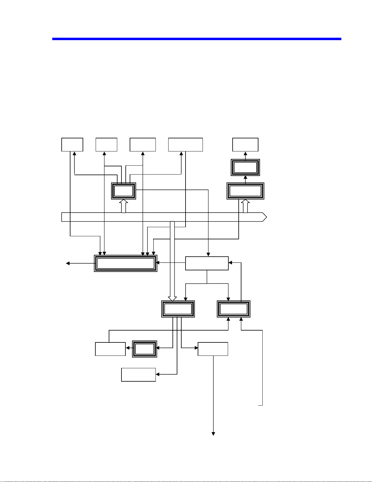
ADMA
(
after accessing 8bit devices. Regarding the PCMCIA and small peripherals,
however, the termination can be delayed by giving an external wait signal.
The GALs which are not shown in this block-diagram are the ARBT and RW32.
• ARBT does the bus arbitration during the DMA’s execution. It also generates a
bus error when the bus cycle passes over the defined time.
• RW32 controls both the RW signals when the DMA is executed and the byteenable signals for the VGA contr oller.
Block Diagram representing relations between I/O Decoding and Acknowledgement
VG SuperI/ MAIN
DR
From CPU
To CPU
Ack)
PCMC
BUS sizer
WaWa
Decod
Flash
71059
GP-IB
NVRAM
RTC
Small
Peripherals
Theory of Operation 4-9
Page 26

4.2 Main Board
Introduction
The main board is divided into the following sections:
Front End
A/D Converter & Memory
Trigger
Timebase
DC Generator
Calibrator & Internal Calibration signal
Signal output
Main Board Control
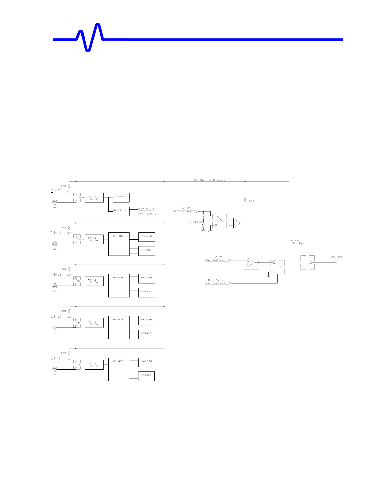
4.2.1 Front End
The front end processes an analog signal for ADC and trigger, consists of High
impedance buffer, am plifier HFE428, and trigg er comparator HTR420.
The main functions of t he Front end without the amplifier HFE428 and HTR420 are:
• Four channels oper at ion, calibration with Software control.
• Input protection (clamp + thermal detection) and coupling (AC, DC, 1MΩ, 50Ω).
• Att enuator by 10 & by 100.
• Offset control.
• Offset control of ±1V and CAL control of ±1.4V.
• Detect ion of 50Ω over loading.
• Input of signal for calibrat ion.
The main functions of HFE428 ar e:
Amplitude normalization for the ADC system : at the BNC the dynamic range is 16
mV to 80V FS (full scale) and the ADC/TRIG system input is 500 mV differential.
Fine adjustment of gain and variable control
Band width limiter of 25MHz, 200MHz
Main function of HFE420 are:
Generation of trig ger signal (analog input and digit al output) with comparator
Setting of trigger level (TRIG,VALIDATE)
Setting of trigger coupling (DC,AC,LFREJ,HFREJ,HF)
Setting of slope (+, - ,WINDO W)
Block diagram 1
4-10 Theory of Operation
Page 27
Control
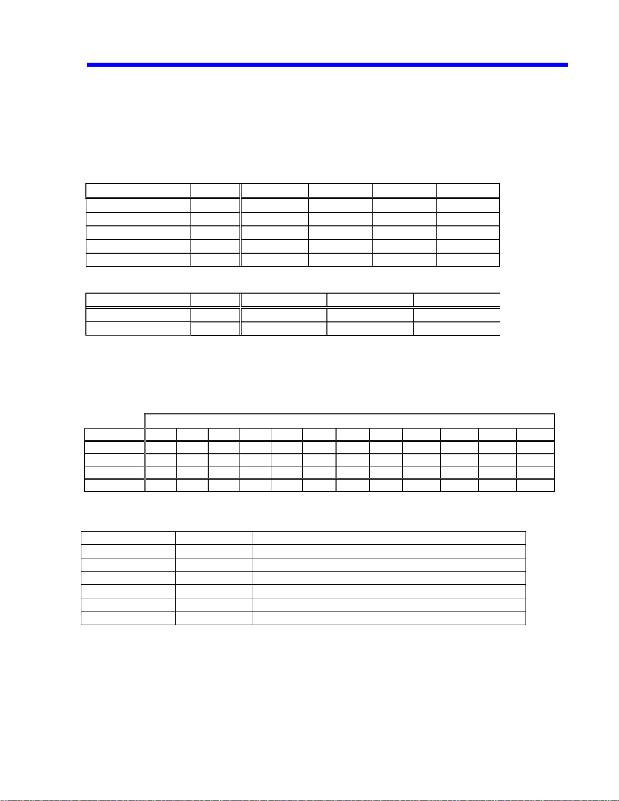
Relay control
The relay of the attenuator is set by selecting the input coupling and the g ain as shown in
the table below.
RL1, 2 and 5 are driven with +5V/0V, and RL3, 4 is driven with +5V/-5V.
Input coupling
Control port Relay GND 1M,DC 1M,AC 50,DC
GND/*MES RL2 H L L L
1M/*50 RL1 H H H L
AC/*DC RL5 H L H L
1/*10 RL3 H X X X
1/*100 RL4 L X X X
Switch of attenuator
Control port Relay 2mV-99mV 100mV-0.99V 1V-10V
1/*10 RL3 H L L
1/*100 RL4 H H L
Divide gain
The gain ratio in each block and input range is a table below.
At the BNC the dynamic range is 16 mV to 80V FS (full scale) and the output is 500 mV
differential (HAD626 input ).
Range V/div
Block
ATT 1/*10
ATT 1/*100
HFE428
Total(ratio)
2mV 5mV 10mV 20mV 50mV 100mV 200mV 500mV 1V 2V 5V 10V
1 1 1 1 1 0.1 0.1 0.1 0.1 0.1 0.1 0.1
1 1 1 1 1 1 1 1 0.1 0.1 0.1 0.1
31.25 12.5 6.25 3.125 1.25 6.25 3.125 1.25 6.25 3.125 1.25 0.625
31.25 12.5 6.25 3.125 1.25 0.625 0.3125 0.125 0.0625 0.03125 0.0125 0.00625
Analog control voltage
Circuit name signal level Signal name
CHx OFFSET +/-4V Offset cont r ol signal
CHx GAIN 0 to +4V HFE428 gain contr ol signal
CHx TRIG LVL1 +/-4V Trigger level control signal
CHx TRIG LVL2 +/-4V Trigger level control signal for smart trigger /window
CHx HYST 0 to +4V Trigger hyster esis control signal
INT CAL 0 to +600mV Signal each CH commonness for calibration
Over load detection
When the input impedance is set to 50 ohm, the over load is detected because of the
protection of the terminating resistance.
Over load signal CHx OVLD is produced by detecting temperat ure of resistance, xR85 for
the load and xR87 for ambient.
It is necessary to measure a standard value when there is no input signal in order to detect
the over load accurately.
The over load is detected by monitoring the difference between this standard value and
Theory of Operation 4-11
Page 28
CHX OVLD.
Calibration
The front end executes the calibration of GAI N, BALANCE when the panel setups and the
ambient temperature change, so guarantees the accuracy.
Block figure 2 shows the supply of the reference voltage INT CAL.
The calibration executes with INT CAL of standard DC voltage.
The INT CAL is all CH common signal and standard DC voltage of the maximum +/600mV.
The INT CAL is attenuated to 1/10 in +/ - 60mV or less.
The CAL OUT signal of DC-1MHz is independent with an internal calibration. The signal
can be monitored with an external terminal by switching the internal calibr at ion signal.
Block diagram 2
4-12 Theory of Operation
Page 29

4.2.2 A/D Converter & Memory
Introduction
The analog to digital converter system does t he signal conversion to 8bit, using the
following circuits:
HAD626
Chip on board MCM (Multi Chip Module).
Hybrid Acquisition Module containing both track & hold am plifier and 8bit ADC.
Differential sig nal input. (Nominal 500mVpp full scale.)
Differential ECL clock input. (up to 500M S/s.)
Differential ECL compat ible data outputs and memory clock.
ECL compatible serial interface for internal ADC gain and offset control.
HMM436
Chip on board MCM.
Hybrid Memory Module containing MAM424.
Maximum buffer length is up to maximum 1Mbytes per channel.
MAM424 (Monolithic Access Memory) captures 8bit data at maximum rate of
500Mbytes/s.
Internal memory consists of a 2Mbit SRAM. (up to 250kbytes per channel.)
HMM436 (LTXXX) : one MAM424 per channel.
HMM436L (LTXXXL): four MAM424’s per channel.
Parallel interface for r eading data and writing registers.
Theory of Operation 4-13
Page 30

4.2.3 Trigger
Introduction
The trigger system includes t he following circuits:
HTR420
Chip on board MCM.
Hybrid TRigger module designed for a trigger conditioning in DSO.
Differential sig nal input. (Nominal 500mVpp full scale.)
Dual threshold inputs controlled by DC generator out put.
Selectable filtering of input signal. (DC, AC, HF REJ, LF REJ)
Frequency divider by four. (HF)
Dual differential ECL outputs. (Trigger signal and qualifier signal)
Single ended analog output for TV trigger.
Serial interface for the internal settings.
TV trigger
This circuit is able to trigger on different TV line number standards.
TV trigger uses a comm er cial chip ( LM1881).
LM1881 generates composite sync output, vertical sync output and odd/even
output.
MST412(Edge qualified function) triggers on video signal using the outputs of
LM1881.
LINE trigger
This circuit makes LINE t rigger signal f r om AC line signal of Power Board.
Polarity of line trigger.
MST412
Trigger functions (Standard trigg er , Hold off, Pulse width, Interval, State qualified,
Edge qualified, Drop out ) are made in Monolithic Smart Trigger.
Dual differential ECL inputs. (Trigger signal and qualifier signal)
Differential ECL clock input.
Differential ECL t r igger output.
Parallel interface for writ ing resisters.
400MHz OSC
generates the 400MHz clock for MST412.
ECL single ended output.
The clock frequency of oscillator is adjustable by analog signal from 8bit DAC.
The clock stops for Standard trigger, Hold off by events, TV trigger and LINE
trigger.
4-14 Theory of Operation
Page 31

A/D CONVERTER & MEMORY Block Diagram
Theory of Operation 4-15
Page 32

4-16 Theory of Operation
Page 33

TRIGGER Block Diagram
Theory of Operation 4-17
Page 34

4-18 Theory of Operation
Page 35

4.2.4 Timebase
Introduction
The timebase system includes the following three cir cuit s :
MTB411A
Monolithic Time Base has five main sections:
TIMEBASE comprises five counters and associated logic circuitr y
for the timebase system.
TDC consists of two counters f or int erpolated and real computation.
TRIGGER is made up of two counters to be used by trigger circuitry.
FREQUENCY is made up of one counter to be used by the main oscillat or circuitry.
DIVIDER consists of a bunch of dividers with mult iplexer for probe calibration pulse.
Parallel interface for reading data and writing resistor.
MCG426
Monolithic Clock Generator.
generates sampling clock for sample & hold up to 500MHz (2GHz).
generates differ ent clocks for MTB411A.
generates MCLR (Master CLeaR) to reset clock divider of HAD626.
generates RAMPST (RAMP STart) signal for Time to Digital Converter.
generates TRT (Test Real Time clock) signal to calibrate 400MHz clock for
MST412.
implements divider and phase detector of a PLL to generate clock system at 2GHz.
Parallel interface for reading data and writing resister.
Time to Digital Converter
measures the time (0 to 2ns) between the trigger and sampling clock using
MTB411A.
The circuit magnif ies t he time by nominal two thousand times.
The magnifying power is adjustable by analog signal from 8bit DAC.
The magnified time is counted by MTB411A using 100MHz clock.
Theory of Operation 4-19
Page 36

Page 37

TIMEBASE Block Diagram
Theory of Operation 4-21
Page 38

4-22 Theory of Operation
Page 39

4.2.5 DC Generator
Introduction
DC generator includes the following cir cuits:
DC Generator
generates analog signals to control Front End offset, HFE428 gain, HTR420
threshold levels and the other circuits.
8bit microprocessor controls DC generat or system.
DC generator uses a commercial 16bit DAC ( DAC712) .
Nominal +/-400mV full scale.
Gain and offset of output are adjusted by analog signals from 8bit DAC.
Analog to Digital Converter
converts analog input signals into digital data. (to detect 50 ohm input overload and
to determine probe type.)
The conversion system consists of 16bit DAC and comparat or .
4.2.6 Calibrator & Internal Calibration Signal
Introduction
generates the probe calibrator signal and internal calibration signal.
Probe calibrator
Continuous gain control using DC gener at or output, -1.0V to +1.0V.
Frequency control using MTB411A’s divider, DC or 500Hz to 1MHz.
Internal calibration signal
Reference voltage signal for internal calibration.
High accuracy, low drift, low noise.
Nominal +/-600mV or +/-60mV output.
The block diagram is included by DC Generat or block diagram.
4.2.7 Signal Output
Introduction
This circuit generates T TL signal for the output of rear panel.
The output signal is selected from trigger ready signal, triggered signal and
PASS/FAIL signal.
The block diagram is included by DC Generat or block diagram.
4.2.8 Main Board Control
Introduction
The Main Board Control includes the following circuits:
Main Board ACK signal generator
generates ACKnowledge signal for a com munication bet ween Main Board and CPU
Board.
HMM436 control
generates special signals for access t o HMM436.
Theory of Operation 4-23
Page 40

generates clock signals f or following components:
MTB411A (16MHz)
IIC BUS chip (8MHz)
8bit microprocessor of DC Generat or (4MHz)
MCG426 control
generates special signals for access t o MCG426.
generates *ATTenuator ENable signal to protect 50ohm input during power-up.
MST412 control
generates special signals for writing commands to MST412.
Serial I/F control
generates the following serial interface signals.
MB SRDI : serial data signal for components except Front End, HAD626 and
HTR420.
MB SRCLK : serial clock signal for components except Front End, HAD626 and
HTR420.
DCG SRCLK : serial clock signal f or 8bit microprocessor of DC generator.
FE SRDI : serial data signal for Front End, HAD626 and HTR420.
FE SRCLK : serial clock signal for Fr ont End, HAD626 and HTR420.
XXXX LD : load signal for serial interface components.
IIC-BUS control
controls Pro-Bus system via serial IIC-bus.
uses a commercial chip (PCF8584).
PCF8584 serves as an interface between parallel bus and the serial IIC-bus.
Thermometer
measures temperature of Main Board.
Acquired data are used to determine condit ion of internal calibration.
EEPROM
4kbit EEPROM.
stores main board calibration data.
8bit D/A Converter
generates analog signal to cont rol trigger hysteresis, TDC gain, clock fr equency for
MST412,
and DAC adjustment of DC gener ator.
uses a commercial chip (MB88346).
MB88346 is 8bit 12channels DAC with output buffers.
Analog signal outputs are 0 to +4.0V full scale.
Main Board Data Read
reads Main Board data for a communication between Main Board and CPU Board.
4-24 Theory of Operation
Page 41

DC GENERATOR Block Diagr am
Theory of Operation 4-25
Page 42

4-26 Theory of Operation
Page 43

MAIN BOARD CONTROL Block Diagram
Theory of Operation 4-27
Page 44

4-28 Theory of Operation
Page 45

4.3 OUTLINE OF WAVERUNNER POWER SUPPLY
Input voltages :W ide rang es of input s, 90∼132 V AC and 180∼250 V AC (45∼66 Hz)
are allowed.
Output voltages: 9 different DC voltages available.
+5 V (DIG)
+12 V (DIG)
+12 V (FAN)
+24 V (PRINTER)
-4.5 V (DIG)
+5 V (ANA)
+12 V (ANA)
- 5 V (ANA)
-12 V (ANA)
This power unit consists of, roughly divided, five independent switching power
supplies and two other circuits.
1. Input circuit (noise filters and rect ifiers are included)
2. Harm onic- cur r ent correction power supply
By employing a step-up converter system, the input current waveform is
controlled to be similar to the waveform of input voltage. The control unit is a
PFC unit made with IC1. The output voltage is r egulated to +377 V DC.
3. Auxiliary power supply (to feed the power for the Harmonic-cur rent control power
supply in the above 2).
Uses an RCC type converter, and outputs +20 V DC.
4. Main power supply-A
Uses a flyback converter, and outputs - 4.5 V DC (DIG ), ±5 V DC ( ANA), and ±12
V DC (ANA) respectively. The output of -4.5 V DC is regulated, but the other
outputs are not regulated and may fluctuate a little in t he voltages depending on
the load conditions.
5. Main power supply-B
Uses a flyback converter, and outputs are +5 V DC (DIG), +12 V DC (DI G), and
+24 V DC (DIG), respectively. The outputs of +5 V DC and +12 V DC are
regulated, but the output of +24 V DC m ay largely fluctuat e according t o the load
conditions.
6. Auxiliary power supply (to feed the power for both Main power supplies- A and B).
Uses an RCC converter, and outputs are +22 V DC and +27 V DC.
7. Series regulator.
Stabilizes the outputs of the main power source of ±5 V DC (ANA), ±12 V DC
(ANA), and reduces the level of ripple noises.
The power switch is located on the secondary side (not the pr imary side) in order to
switch-on and -off of t he outputs at the secondary side; the whole contr ol is made
by switching on and off of the current control oscillator which is config ured with the
IC 2 and IC6. Although the power switch is placed to its off position, t herefore, the
power is being fed to all the components in t he power supply units (st and-by m ode),
as long as the waverunner supply is connected to the AC outlet.
The above switching-on and -off f unction is actually made by shorting and opening
of pins 6 and 7 of "CN3" in the power unit.
Since the design of this waverunner power supply is made based on the use of
Theory of Operation 4-29
Page 46

forced air cooling with the fan-motors, operating the power supply for long hours by
removing the upper and bottom covers would cause tripping of the overheat
protection circuit because of a tem perature rise in the unit, and result in the cease
of power output.
The DC outputs are all guarded by the overload-current protection circuits;
therefore, output short cir cuiting will not cause any damage t o the eq uipment even it
takes place. However, when the short-circuited state continues for long hours, the
power output switch may cause open due to a possible temperature rise in several
circuits, causing the excess-current protecting circuit to activate.
Releasing of the overheat protection circuit from its activated mode must not be
made within the time less than five seconds by disconnecting the AC inlet plug out
of the AC receptacle.
Do not touch any electric parts inside the power supplies during operation as the
primary side of the power unit has many portions of over 500 Vrms of magnitudes to
grounding.
< Operation of the parts inside the Waverunner Power Supply>
# Circuit No. 1 / 7
The fuse, F1, heat-breaks to shut down the input when an abnormal excess-current
keeps running through t he input circuit. Replacing of the f use must be made after
locating the problem area and fixing failure parts (including damag es) .
The coils, L2, L3, L4, and L5, and capacitors, C1, C2, C3, C4, C5, C6, C94, and
C105, configure the circuits of noise filters to the AC power lines.
The resistor, R2, which contains a thermo-fuse, is to limit the in-r ush current when it
flows into the input circuit. In case an abnormal input current keeps flowing, even
when the power switch(through switching operation) is placed to off, the thermofuse melts down and disconnects the input circuit.
When the switching power supplies operate normally, the TRIAC, D2, turns on to
bypass the R2 current, to reduce R2's electric losses dur ing the operation.
The diode, D4, is a bridge circuit and is used for direct f ull wave rectification of the
AC input.
# Circuit No. 2 / 7
The IC1 in the PFC unit receives its operating power from the auxiliary power supply
which consists of the transistor Q2 and transformer T1, etc; outputs the driving
signals (Gate Signals) for the transistor Q1, and operates the Harmonic control
power supply which consists of the choking coil L6, diode D5, capacitors C13, etc.,
to obtain the output of +377 V DC.
The variable resistor, R16, is to adjust the output voltage of +377 V DC in the
Harmonic control power source.
4-30 Theory of Operation
Page 47

#Circuit No. 3 / 7
The variable resistor, R117, is to adjust the output voltage of -4.5 V DC.
# Circuit No. 4 / 7
The outputs of ±5 V DC (ANA) and ±12 V DC (ANA) use the series regulator,
consisting of the transistor s Q10 t o Q18 and I C9, which stabilizes the output voltag e
and reduces the ripple voltages. Also, the series regulator performs the remote
sensing function (by using No. 2 to No. 5 pins of Connector CN3) in order to keep
the voltage of the main-board on the load side constant.
The variable resistor, R152, is for controlling the DC output voltages of ±5 V (ANA)
and ±12 V ( ANA). The DC output voltages of ±5 V (ANA) and ±12 V (ANA) are the
tracking outputs (voltages of 4 outputs vary with each other).
# Circuit No. 5 / 7
The variable resistor, R73, is used to adjust the regulated output voltage of +5 V DC
(DIG).
#Circuit No. 6 / 7
The posistor, R 33, shows high resistance property when its temperature increases
over 90°C (due to the temperature rises in Q10 or Q12), and stops IC2 and IC6
oscillations, causing disconnection of the voltage out put circuits (through activation
of the overheat protection circuit). Releasing of the overheat protection circuit f rom
its activated mode must be made by confirming the heat-sink temperature of the
protection circuit to be cooled under 80°C, by leaving the unit more than five
seconds while the AC inlet plug out of the AC receptacle is disconnect ed.
The posistor, R160, becomes high resist ance when its temperature increases over
80°C (due to the temperature rises in Q14 or Q16), and stops IC2 and IC6
oscillations, causing disconnection of the voltage out put circuits (through activation
of the overheat protection circuit). Releasing of the overheat protection circuit f rom
its activated mode must be made by confirming the heat-sink temperature of the
protection circuit to be cooled under 70°C, by leaving the unit more than five
seconds while the AC inlet plug out of the AC receptacle is disconnect ed.
The posistor, R166, becomes high resistance when the temperature of R 166
increases over 110°C due to the temperature rise in Q1, and stops IC2 and IC6
oscillations which cause disconnection of the voltage output circuits (through
activation of the overheat protection circuit). Releasing of the overheat protection
circuit from its activated mode must be made by confirming the heat-sink
temperature of the protection circuit to be cooled under 100°C, by leaving the unit
more than five seconds while the AC inlet plug out of the AC receptacle is
disconnected.
# Circuit No. 7 / 7
The IC2 in the circuit of t he switching power control ICs receives the power which is
fed by the auxiliary power supply (circuit No.6/7) consisting of the transist or Q4 and
the transformer T2, to out put the driving signals (G ate signals) for the transistor Q6
(circuit No.5/7); and drives the Main power supply-A (circuit No. 5/7) consisting of t he
Theory of Operation 4-31
Page 48

transformer T3 and others. The Main power supply-A generates the output voltages
of +5 V DC (for DIG Circuit), +12 V DC (for DI G Cir cuit and Fan) , and +24 V DC ( f or
Printer), respectively.
The IC6 in the circuit of t he switching power control ICs receives the power which is
fed by the auxiliary power supply (circuit No.6/7) consisting of the transist or Q4 and
the transformer T2, to out put the driving signals (G ate signals) for the transistor Q8
(circuit No.3/7); and drives the Main power supply-B (circuit No. 3/7) consisting of t he
transformer T4 and others. The Main power supply-B generates the output voltages
of ±5 V DC (for ANA circuit), ±12 V DC (for ANA circuit), and -4.5V DC (for DIG
circuit).
4-32 Theory of Operation
Page 49

BLOCK DIAGRAM of FND POWER SUPPLY
Theory of Operation 4-33
Page 50

5. Performance Verification
5.1 Introduction
This chapter contains procedures suitable for determining if the LT Series Digital
Storage Oscilloscope performs correctly and as warranted.
They check all the characteristics listed in subsection 5.1.1.
Because they require time and suitable test equipment, you may not need to
perform all of these procedures, depending on what you want to accomplish.
In the absence of the computer automated calibration system based on LeCroy
Calibration Software (LeCalsoft), this manual performance verification procedure
can be followed to establish a traceable calibration.
It is the calibrating entities’ responsibility to ensure that all laboratory standards
used to perform this procedure are operating within their specifications and
traceable to required standards if a traceable calibration certificate is to be issued
for the LT Series Digital Storage Oscilloscope.
5.1.1 List of Tested Characteristics
This subsection lists the characteristics that are tested in terms of quantifiable
performance limits.
• Input Impedance
• Leakage Current
• Noise
• DC Gain Accuracy
• Offset Accuracy
• Bandwidth
• Trigger Level
• Smart Trigger
• Time Base Accuracy
• Overshoot and Rise Time
• Overload
5.1.2 Calibration Cycle
The LT Series Digital Storage Oscilloscope requires periodic verification of
performance. Under normal use ( 2,000 hours of use per year ) and environmental
conditions, this instrument should be calibrated once a year.
Performance Verification 5-1
Page 51

5.2 Test Equipment Required
These procedures use external, traceable signal generators, DC precision power
supply, step generator and digital multimeter, to directly check specifications.
Instrument Specifications Recommended
Signal Generator
Radio Frequency
Signal Generator
Audio Frequency
Voltage Generator
DC Power Supply
Step Generator
Fast Pulser
Power Meter +
Sensor
Digital Multimeter
Volt & Ohm
Adapter
Coaxial Cable, 1 ns
Coaxial Cable, 5 ns
2 Attenuators, 20 dB
Attenuator, 6 dB
Terminator, 2 W
T adapter
Frequency : .5 MHz to 2 GHz
Frequency Accuracy : 1 PPM
Frequency : 0 to 5 kHz
Amplitude : 8 V peak to peak
Range of 0 to 20 V, in
steps of no more than 15 mV
Rise time 350ps ± 100 ps
Overshoot 3.5 % ± 1 %
Accuracy ±1 %
Voltmeter Accuracy : 0.1 %
Ohmmeter Accuracy : 0.1 %
50Ω to 1MΩ
50Ω, BNC, length 20 cm,
50Ω, BNC, length 100 cm,
50Ω, BNC, 1 % accuracy
50Ω, BNC, 1 % accuracy
50Ω, BNC, Feed-Through
50Ω, BNC T adapter
HP8648B
or equivalent
LeCroy LW420
or HP33120A or
equivalent
HP6633A
or equivalent
LeCroy 4969A + PB049
or equivalent
HP437B + 8482A or
equivalent
Keithley 2000
or equivalent
LeCroy 4962-9
LeCroy 480232001
LeCroy 480020101
LeCroy 402200402
LeCroy 402600403
LeCroy 402323001
LeCroy 402222002
5.2.1 Test Records
The last pages of this document contain LT Series test records in the format
tables. Keep them as masters and use a photocopy for each calibration.
5.3 Turn On
If you are not familiar with operating the LT Series, read the operator's manual.
§ Switch on the power using the power switch.
§ Wait for about 20 minutes for the scope to reach a stable operating
temperature, and verify
5-2 Performance Verification
Table 5-1 : Test Equipment
Page 52

5.3.1 PNL Files
§ Use PNL Files depend on the LT344,LT342,LT322,LT224.
§ The LTxxx shows one of the LT344,LT342,LT322,LT224.
5.4 Input Impedance
The impedance values for 50Ω and 1MΩ couplings are measured with a high
precision digital multimeter. The DMM is connected to the DSO in 4 wire
configuration (input and sense), allowing for accurate measurements.
Specifications & Test limits
DC 1.00 MΩ ±1 %
AC 1.20 MΩ ±1 % (2mV/div to 99mV/div)
1.00 MΩ ±1 % (100mV/div to 10V/div)
DC 50Ω ±1 %
5.4.1 Channel Input Impedance
a. DC 1MΩ
§ Recall LTxxxP001.PNL or configure the DSO :
Panel Setups : Recall FROM DEFAULT SETUP
Channels Trace OFF Channel 1, Channel 2, Channel 3 & Channel 4
Input Coupling : DC 1MΩ on all 4 Channels
Input gain : 50 mV/div. on all 4 Channels
Time base : 50 nsec/div.
Trigger mode : Auto
Performance Verification 5-3
Page 53

§ Set the DMM with Ohms and Ohms sense to provide a 4 wire measurement.
§ Connect it to Channel 1.
§ Measure the input impedance. Record it in Table 2, and compare it to the
limits.
§ Repeat the above test for all input channels.
§ Recall LTxxxP002.PNL or Set Input gain to 200 mV/div. on all 4 Channels
§ Repeat the test for all input channels.
§ Record the measurements in Table 2, and compare the test results to the
limits in the test record.
b. AC 1MΩ
§ Recall LTxxxP003.PNL or configure the DSO as shown in 5.4.1.a,
and for each Channel make the following change :
Input Coupling : AC 1MΩ
5-4 Performance Verification
Page 54

§ For all input channels measure the input impedance.
§ Record the input impedance in Table 2, and compare it to the limits.
§ Recall LTxxxP004.PNL or Set Input gain to 200 mV/div on all 4 Channels.
§ Repeat the test for all input channels.
§ Record the measurements in Table 2, and compare the results to the limits in
the test record.
c. DC 50Ω
§ Recall LTxxxP005.PNL or configure the DSO as shown in 5.4.1.a,
and for each Channel make the following change:
Input Coupling : DC 50Ω
Performance Verification 5-5
Page 55

§ For all input Channels, measure the input impedance.
§ Record the input impedance in Table 2, and compare it to the limits.
§ Recall LTxxxP006.PNL or set Input gain to 200 mV/div. on all 4 Channels
§ Repeat the test for all input channels. Record the measurements in Table 2,
and compare the results to the limits in the test record.
5.4.2 External Trigger Input Impedance
a. DC 1MΩ
§ Recall LTxxxP007.PNL or configure the DSO :
Trigger mode : Auto
Select Setup trigger
Trigger on : EXT
Cplg Ext : DC
External : DC 1MΩ
Time base : 50 nsec/div.
5-6 Performance Verification
Page 56

§ Connect the DMM to External, and measure the input impedance.
§ Record the input impedance in Table 2, and compare it to the limits.
§ Recall LTxxxP008.PNL or set trigger to Ext/10
§ Measure the input impedance.
§ Record the test result in Table 2, and compare the result to the limits in
the test record.
b. DC 50Ω
§ Recall LTxxxP009.PNL or configure the DSO :
Select Setup trigger
Trigger on : EXT
External : DC 50Ω
Performance Verification 5-7
Page 57

§ Connect the DMM to External, and measure the input impedance.
§ Record the input impedance in Table 2, and compare the result to the limit in
the test record.
5-8 Performance Verification
Page 58

5.5 Leakage Current
The leakage current is tested by measuring the voltage across the input channel.
Test limit
DC 1MΩ : ±1 mV
5.5.1 Channel Leakage Current
§ Recall LTxxxP010.PNL or configure the DSO :
Panel Setups : Recall FROM DEFAULT SETUP
Channels Trace ON Channel 1, Channel 2, Channel 3 & Channel 4
Input Coupling : DC 1MΩ on all 4 Channels
Input gain : 50 mV/div. on all 4 Channels
Trigger mode : Auto
Time base : 10 µsec/div.
§ Set the DMM to measure Volts, and connect it to Channel 1.
§ Measure the voltage and enter it in Table 3. Compare it to the limits.
§ Repeat the test for all input channels.
Performance Verification 5-9
Page 59

5.5.2 External Trigger Leakage Current
a. DC 50Ω
§ Recall LTxxxP011.PNL or configure the DSO as shown in 5.5.1
and make the following changes :
Select Setup trigger
Set Trigger on : EXT
External : DC 50Ω
§ Connect the DMM to External.
§ Measure the voltage and enter it in Table 3. Compare it to the limits.
5-10 Performance Verification
Page 60

5.6 Noise
Noise tests with open inputs are executed on all channels for both 1MΩ and 50Ω input
impedance, with AC and DC input coupling, 0 mV offset, at a gain setting of 5mV/div.,
and different Time base settings.
The scope parameters functions are used to measure the RMS amplitude.
5.6.1 Rms Noise
Test limits
1 % of full scale or 0.4 mV rms at 5 mV/div.
Procedure
a. DC 1MΩ
With no signal connected to the inputs
§ Recall LTxxxP012.PNL or configure the DSO :
Panel Setups : Recall FROM DEFAULT SETUP
Channels Trace ON Channel 1, Channel 2, Channel 3 & Channel 4
Input Coupling : DC 1MΩ on all 4 Channels
Input gain : 5 mV/div. on all 4 Channels
Trigger setup : Edge
Trigger on : 1
Coupling 1 : DC
Trigger Mode : Auto
Time base : 20 msec/div.
Channel use : 4
Record up to : 50 k Samples
Press : MEASURE TOOLS
Measure : Parameters
Mode : Custom
Statistics : On
Change parameters
Category : All
On line 1 : Measure sdev of Ch1
On line 2 : Measure sdev of Ch2
On line 3 : Measure sdev of Ch3
On line 4 : Measure sdev of Ch4
On line 5 : no parameter selected for line 5
Performance Verification 5-11
Page 61

§ Press Clear Sweeps.
§ Measure for at least 50 sweeps, then press Stop to halt the acquisition.
§ Record the four high sdev parameter values in Table 4, and compare the test
results to the limits in the test record.
§ Repeat the test for Time base : 1 msec/div., 50 µsec/div., and 2 µsec/div.
§ Record the measurements (high sdev of 1,2,3,4) in Table 4, and compare the
results to the limits in the test record.
b. AC 1MΩ
§ Recall LTxxxP013.PNL or configure the DSO as shown in 5.6.1
and for each Channel make the following change :
Input Coupling : AC 1MΩ on all 4 Channels
Time base : 2 µsec/div.
§ Press Clear Sweeps.
§ Measure for at least 50 sweeps, then press Stop to halt the acquisition.
5-12 Performance Verification
Page 62

§ Record the four high sdev parameter values in Table 4, and compare the test
results to the limits in the test record.
Performance Verification 5-13
Page 63

c. DC 50Ω
§ Recall LTxxxP014.PNL or configure the DSO as shown in 5.6.1
and make the following changes :
Input Coupling : DC 50Ω on all 4 Channels
Time base : 2 µsec/div.
§ Press Clear Sweeps.
§ Measure for at least 50 sweeps, then press Stop to halt the acquisition.
§ Record the four high sdev parameter values in Table 4, and compare the test
results to the limits in the test record.
§ Repeat the test for Time base : 20 µsec/div.
§ Record the measurements (high sdev of 1,2,3,4) in Table 4, and compare the
results to the limits in the test record.
5-14 Performance Verification
Page 64

5.6.2 Erroneous Read / Write Test
Test limit
±2.5 % of full scale at 50 mV/div.
Procedure
a. Channel 1, Channel 2, Channel 3 and Channel 4
§ For LT Series recall LTxxxP015.PNL,
for LT 34XL recall LT344 P016.PNL.
Channels Trace ON Channel 1, Channel 2, Channel 3 & Channel 4
Zoom+Math Trace ON D
Input Coupling : DC 50Ω on all 4 Channels
Global BWL ON : 25MHz
Input gain : 50 mV/div. on all 4 Channels
Offset : Zero on all 4 Channels
Trigger on : Line
Trigger mode : Normal
Time base : 50 µsec/div for LT344, LT342, LT322 and LT224
200us/div for LT344L and LT342L
Select Setup timebase
Channel use : 4
Record up to : 100K samples for LT322 and LT224
250K samples for LT344 and LT342
1M samples for LT344L and LT342L
Select Math Setup
For Math : Use at most 500 points
Redefine A : A=1-1
Use Math? : Yes
Math Type : Arithmetic
Difference : 1 minus 1
Redefine B : B=2
Use Math? : No
Trace B is Zoom of 2
Redefine D : D=M1
Use Math? : No
Trace D is Zoom of M1
Performance Verification 5-15
Page 65

§ Press Reset Zoom+Math
§ Press MEASURE TOOLS
Measure : Parameters
Mode : Pass
Testing : On
Select : Change Test Conditions
On line : Action
If : Fail
Then : Stop Yes
Store No
Dump No
Beep Yes
Pulse No
On line 1 : Test on Mask
True if all points of 1 are inside mask D
On line 2 : Test on Mask
True if all points of 2 are inside mask D
On line 3 : Test on Mask
True if all points of 3 are inside mask D
On line 4 : Test on Mask
True if all points of 4 are inside mask D
5-16 Performance Verification
Page 66

Performance Verification 5-17
Page 67

5-18 Performance Verification
Page 68

§ Select Modify Mask
From : W'form
Into : M1
Use W'form : A
Delta V : 0.20 div
Delta T : 0.00 div
§ To start the test, select MEASURE TOOLS, Change Test Conditions,
Modify Mask and press Make Mask M1
§ After 1000 sweeps for LT322 and LT224, or 400 sweeps for LT344 and
LT342, or after 100 sweeps for LT344L check that the number of Passed equals
the number of Sweeps on all 4 Channels.
§ Record the test result in Table 5.
Performance Verification 5-19
Page 69

5.7 DC Accuracy
This test measures the DC Accuracy of the absolute voltage measurements at
0V offset setting.
It requires a DC source with a voltage range of 0 V to 20 V adjustable in steps of
no more than 15 mV, and a calibrated DMM that can measure voltage to 0.1 %.
Measurements are made using voltage values applied by the external
voltage reference source, measured by the DMM, and in the oscilloscope using
the parameters Std voltage.
For each known input voltage, the deviation is checked against the tolerance.
Specification & Test limits
±(0.015 x | Vm + Voffset | + 0.015 x | Voffset| + 0.01 x FS + 1mV)
Vm [volts] = voltage reading [volts]
FS [volts] = 8[div] x sensitivity [volt/div]
Voffset [volts] = setting offset voltage [volts]
Procedure
§Recall LTxxxP017.PNL or configure the DSO:
Panel Setups : Recall FROM DEFAULT SETUP
Channels Trace ON Channel 1, Channel 2, Channel 3 & Channel 4
Input Coupling : DC 1MΩ on all 4 Channels
Input offset : 0.0 mV on all 4 Channels
Input gain : from 2mV/div to 1 V/div and 5V/div. (see Table 6) on
all 4 Ch
Trigger setup : Edge
Trigger on : line
Slope line : Positive
Mode : Auto
Time base : 2 msec/div.
Channel use : 4
Record up to : 25 k
Channels Trace OFF Channel 1, Channel 2, Channel 3 & Channel 4
MATH TOOLS Trace ONA, B, C & D
Select Math Setup
For Math : Use at most 5000 points
Redefine A, B, C, D Channel 1, Channel 2, Channel 3 & Channel 4
Use Math ? : Yes
Math Type : Average
Avg. Type : Summed
For : 100 sweeps
MEASURE TOOLS : Parameters
Mode : Custom
5-20 Performance Verification
Page 70

Statistics : off
Change parameters
On line 1 : Measure mean of A
On line 2 : Measure mean of B
On line 3 : Measure mean of C
On line 4 : Measure mean of D
§ For the low sensitivities: 2 mV, 5 mV, 10 mV and 20 mV/div., connect the test
equipment as shown in Figure 5-1.
§
LC584AL 1GHz Oscilloscope
Figure 5-1: DC 1MΩ Accuracy Equipment Setup for 2,5,10 and 20 mV/div.
§ For 100 mV/div, connect the test equipment as shown in Figure 5-2.
§ For 5V/div no attenuator is required, connect the test equipment as shown in
Figure 5-3.
Performance Verification 5-21
Page 71

LC584AL 1GHz Oscilloscope
Figure 5-2 : DC 1MΩ Accuracy Equipment Setup for 100 mV/div
LC584AL 1GHzOscilloscope
Figure 5-3 : DC 1MΩ Accuracy Equipment Setup for 5V/div.
5-22 Performance Verification
Page 72

§ For each DSO Volts/div, set the output of the external DC voltage reference
source as shown in Table 6, column PS output.
1) Connect the DMM and record the voltage reading in Table 6, column DMM.
2) Disconnect the DMM from the BNC T connector.
3) Press Clear Sweeps
4) After 100 sweeps, read off the DSO mean parameter, and record the
measurement in Table 6, column Mean.
§ For each DC voltage applied to the DSO input, repeat parts 1), 2), 3) and 4).
§ Calculate the Difference ( ∆ ) by subtracting the DMM voltage reading from
the DSO mean voltage reading. Record the test result in Table 6, and compare
the Difference ( ∆ ) to the corresponding limit in the test record.
§ Repeat step 5.7 Procedure for the other channels, substituting channel controls
and input connector.
Performance Verification 5-23
Page 73

5.8 Offset Accuracy
The offset test is done at 5mV/div, with a signal of ±1 Volt cancelled by an offset
of the other polarity.
Specifications
± (0.015 x Voffset + 0.005 x FS + 1mV)
FS [volts] = 8[div] x sensitivity[volts/div]
Voffset [volts] = setting offset voltage
Procedure
§ Recall LTxxxP018.PNL or configure the DSO:
Panel Setups : Recall FROM DEFAULT SETUP
Channels Trace ON Channel 1, Channel 2, Channel 3 & Channel 4
Input Coupling : DC 1MΩ on all 4 Channels
Input gain : 5mV/div on all 4 Channels
Input offset : +1 Volt on all 4 Channels
Trigger setup : Edge
Trigger on : 1
Coupling 1 : DC
Mode : Auto
Time base : 2 msec/div.
Channel use : 4
Record up to : 25 k
Channels Trace OFF Channel 1, Channel 2, Channel 3 & Channel 4
Zoom+Math Trace ON A, B, C & D
Select Math Setup
For Math : Use at most 5000 points
Redefine A, B, C, D Channel 1, Channel 2, Channel 3 & Channel 4
Use Math ? : Yes
Math Type : Average
Avg. Type : Summed
For : 100 sweeps
MEASURE TOOLS: Parameters
Mode : Custom
Statistics : off
5-24 Performance Verification
Page 74

§ Connect the test equipment as shown in Figure 5-4.
LC584AL 1GHz Oscilloscope
§ Set the output of the external DC voltage reference source to −1 Volt.
1) Verify that the displayed trace A : Average (1) is on the screen, near the
center horizontal graticule line. If the trace is not visible, modify the DC voltage
reference source output until the trace is within ± 2 divisions of center.
2) Connect the DMM and record the voltage reading in Table 7, column DMM.
3) Disconnect the DMM from the BNC T connector.
4) Press Clear Sweeps
5) After 100 sweeps, Read off the DSO Mean parameter voltage, and record
the measurement in Table 7, column Mean.
§ Repeat the test for the other channels, substituting channel controls and input
connector. Record the measurements in Table 7.
§ Repeat the test the other offset settings –1V and 0V.
Recall LTxxxP019.PNL for Input offset –1V.
Recall LTxxxP020.PNL for Input offset 0V.
Performance Verification 5-25
Page 75

Record the measurements in Table 7.
§ Calculate the Difference ( ∆ ) by subtracting the DMM voltage reading from
the DSO mean voltage reading.
§ Record the test result in Table 7, and compare the Difference ( ∆ ) to the
corresponding limit in the test record.
5-26 Performance Verification
Page 76

5.9 Bandwidth
The purpose of this test is to ensure that the entire system has a bandwidth of at
least 500MHz or 200MHz. An external source is used as the reference to provide
a signal where amplitude and frequency are well controlled.
The amplitude of the generator as a function of frequency and power is calibrated
using an HP8482A sensor on an HP437B power meter or equivalent.
Specifications & Test limits
DC to 500MHz (10mV to 5V/div) for LT344/L, LT342/L, LT322
DC to 200MHz (5mV to 10V/div) for LT224
Procedure
§ Recall LTxxxP021.PNL or configure the DSO
Panel Setups : Recall FROM DEFAULT SETUP
Channels Trace ON Channel 1, Channel 2, Channel 3 & Channel 4
Input Coupling : DC 50Ω on all 4 Channels
Input gain : 50 mV/div on all 4 Channels
Input offset : 0 mV on all 4 Channels
Trigger setup : Edge
Trigger on : Line
Slope line : Pos
Mode : Auto
Time base : 1 µsec/div.
Channel use : 4
Record up to : 25 k
MEASURE TOOLS : Parameters
Mode : Custom
Statistics : On
Change parameters
On line 1 : Sdev of 1
On line 2 : Sdev of 2
On line 3 : Sdev of 3
On line 4 : Sdev of 4
§ Connect the HP8482A power sensor to the power meter.
§ Zero and calibrate the HP8482A power sensor using the power meter Power
Ref output.
§ Connect a BNC adapter to the HP8482A power sensor.
Performance Verification 5-27
Page 77

§ Connect a 5ns 50Ω BNC cable to the RF output of the HP8648B
generator and then through a 6dB attenuator and the necessary adapters to
the power sensor.
Figure 5-5 : Power Meter Equipment Setup
§Set the generator frequency to 300 kHz
§Set the generator amplitude to measure 0.200 mW on the power meter.
§Read the displayed generator output amplitude, and record it in the third
column of Table 8.
§Repeat the above measurement for 1.1 MHz, 10.1 MHz, 100.1 MHz,
200.1MHz,
300.1 MHz & 500.1 MHz. Record the generator output amplitude readout in the
third column of Table 8.
§ Disconnect the RF output of the HP8648B generator from the HP8482A power
sensor.
§ Connect the RF output of the HP8648B generator through a
5ns 50 Ohm BNC cable and a 6 dB attenuator into Channel 1.
§ Set the generator frequency to 300 kHz.
§ From the generator, apply the recorded generator signal amplitude to
Channel 1.
§ Press Clear Sweeps.
5-28 Performance Verification
Page 78

LC584AL 1GHz Oscilloscope
Figure 5-6 : 50Ω Bandwidth Equipment Setup
§ Measure for at least 100 sweeps, record the average value of sdev(1) I
nTable 8
§ Repeat the above 3 steps for Channel 2, Channel 3 & Channel 4 substituting
channel controls and input connector. Record the measurements in Table 8.
§ Repeat the above measurement for all channels for 1.1 MHz, 10.1 MHz,
100.1 MHz, 200.1MHz, 300.1 MHz and 500.1 MHz and record the values in
Table 8.
§ Calculate the ratio to .3MHz for each frequency.
Ratio = (sdev of XXXMHz) / (sdev of 0.3MHz)
and compare the results to the limits in the test record.
Performance Verification 5-29
Page 79

§ Recall LTxxxP022.PNL or configure the DSO as shown in 5.9 and for
each Channel make the following change :
Input gain : 100mV/div
§ Connect the test equipment as shown in Figure 5-5.
§ Set the generator frequency to 300 kHz
§ Set the generator amplitude to measure 0.800 mW on the power meter.
§ Read the displayed generator output amplitude, and record it in the third
column of Table 9.
§ Repeat the above measurement for 1.1 MHz, 10.1 MHz, 100.1 MHz, 200.1MHz,
300.1 MHz & 500.1 MHz. Record the generator output amplitude readout in the
third column of Table 9.
§ Disconnect the RF output of the HP8648B generator from the HP8482A power
sensor.
§ Connect the test equipment as shown in Figure 5-6.
5-30 Performance Verification
Page 80

§ Set the generator frequency to 300 kHz.
§ From the generator, apply the recorded generator signal amplitude to
Channel 1.
§ Press Clear Sweeps.
§ Measure for at least 100 sweeps, record the average value of sdev(1) in Table
9
§ Repeat the above 3 steps for Channel 2, Channel 3 & Channel 4 substituting
channel controls and input connector. Record the measurements in Table 9.
§ Repeat the above measurement for all channels for 1.1 MHz, 10.1 MHz,
100.1 MHz, 200.1MHz, 300.1 MHz and 500.1 MHz and record the values in
Table 9.
§ Calculate the ratio to .3 MHz for each frequency.
Ratio = (sdev of XXXMHz) / (sdev of 0.3MHz)
and compare the results to the limits in the test record.
b. DC 50Ω with Bandwidth Limiter On
§ Recall LTxxxP023.PNL or configure the DSO:
Panel Setups : Recall FROM DEFAULT SETUP
Channels Trace ON Channel 1
Input Coupling : DC 50Ω
Global BWL : 25 MHz
Input gain : 100 mV/div.
Input offset : 0 mV
Trigger setup : Edge
Trigger on : 1
Slope line : Pos
Mode : Auto
Time base : 1 µsec/div.
Channel use : 4
Record up to : 25 k
MEASURE TOOLS : Parameters
Mode : Custom
Statistics : Off
Change parameters
On line 1 : Sdev of 1
On line 2 : Freq of 1
§ Connect the test equipment as shown in Figure 5-6.
Performance Verification 5-31
Page 81

§ Set the generator frequency to 300 kHz.
§ Adjust the generator signal amplitude to measure sdev(1) = 200 mV.
§ Set Time base : 50 nsec/div.
§ Increase the generator frequency until sdev(1) = 140 mV. (typically 25 MHz)
§ Press Clear Sweeps
§ When sdev(1) = 140 mV, record Freq(1) in Table 10.
§ Check that the frequency is within the limits specified in Table 10.
5-32 Performance Verification
Page 82

The following test of BWL: 200MHz is not applied for LT224.
§ Set Global BWL : 200 MHz
§ Set Timebase : 5 nsec/div.
§ Increase the generator frequency until sdev(1) = 140 mV. (typically 200 MHz)
Performance Verification 5-33
Page 83

§ Press Clear Sweeps
§ When sdev(1) = 140 mV, record Freq(1) in Table 10.
§ Repeat the 25 MHz and 200 MHz Bandwidth limiter tests for the other
channels, substituting channel controls and input connector.
§ Recall LTxxxP024.PNL for Channel 2, LTxxxP025.PNL for Channel3
LTxxxP026.PNL for Channel 4, or configure the DSO as shown in 5.9.1
Procedure and make the necessary changes.
§ Record the test results in Table 10, and compare the results to the limits.
5-34 Performance Verification
Page 84

5.10 Trigger Level
The trigger capabilities are tested for several cases of the standard edge trigger:
§ Channel (internal), and External Trigger sources
§ Three DC levels: −3, 0, +3 major screen divisions
§ DC, HFREJ coupling
§ Positive and negative slopes
5.10.1 Channel Trigger at 0 Division Threshold
a. DC Coupling
Recall LTxxxP027.PNL or configure the DSO:
Panel Setups : Recall FROM DEFAULT SETUP
Channels Trace ON Channel 1, Channel 2, Channel 3 & Channel 4
Input Coupling : DC 50Ω on all 4 Channels
Input gain : 100 mV/div. on all 4 Channels
Input offset : 0 mV on all 4 Channels (use show status to verify)
Trigger setup : Edge
Trigger on : 1
Slope 1 : Pos
Coupling : DC
Mode : Auto
Set Trigger level : DC 0.0 mV
Pre-Trigger Delay : 50 %
Time base : 0.1 msec/div.
Record up to : 50 k samples
Channels Trace OFF Channel 1, Channel 2, Channel 3 & Channel 4
Zoom+Math Trace ON A, B, C & D
Select Math Setup
For Math : Use at most 5000 points
Redefine A, B, C, D Channel 1, Channel 2, Channel 3 & Channel 4
Use Math ? : Yes
Math Type : Average
Avg. Type : Summed
For : 10 sweeps
Performance Verification 5-35
Page 85

§ Set the output of the LeCroy LW420 or equivalent audio frequency signal
generator to 1 kHz.
§ Connect the output of the generator to Channel 1 through a 50 Ohm coaxial
cable and adjust the sine wave output amplitude to get 8 divisions peak to
peak .
§ Select MEASURE TOOLS : Cursors, Time, Absolute
§ Use the "cursor position" knob, to move the Time marker at 0.0 µs
§ Press Clear Sweeps,
§ Acquire 10 sweeps and record in Table 11 the level readout displayed below
100 mV in the icon 1, at top left.
§ Compare the test results to the corresponding limit in the test record.
§ Set Trigger Slope 1 : Neg
§ Acquire 10 sweeps and record in Table 11 the level readout displayed below
5-36 Performance Verification
Page 86

100 mV in the icon 1, at top left.
b. HFREJ Coupling
§ Set Coupling : HFREJ
§ Acquire 10 sweeps and record in Table 12 the level readout displayed below
100 mV in the icon 1, at top left.
§ Set Trigger Slope 1 : Pos
§ Acquire 10 sweeps and record in Table 12 the level readout displayed below
100 mV in the icon 1, at top left.
§ Repeat steps 5.10.1.a. and 5.10.1.b. for all input channels, substituting channel
controls ( DC, HFREJ, Pos, Neg ) and input connector.
Recall LTxxxP028.PNL for Channel 2, LTxxxP029.PNL for Channel 3,
LTxxxP030.PNL for Channel 4, or select Trigger on the Channel under
test.
The Trigger level is displayed in either the icon 2, 3 or 4
Performance Verification 5-37
Page 87

§ Record the measurements in Table 11 & 12 and compare the test results to the
corresponding limits in the test record.
5.10.2 Channel Trigger at +3 Divisions Threshold
a. DC Coupling
§ Recall LTxxxP031.PNL or configure the DSO as shown in 5.10.1.a and for
each Channel make the following change :
Set Trigger level : DC +300 mV
§ Connect the output of the generator to Channel 1 through a 50 Ohm coaxial
cable.
§ Press Clear Sweeps,
§ Acquire 10 sweeps and record in Table 11 the level readout displayed below
100 mV in the icon 1, at top left.
§ Compare the test results to the corresponding limit in the test record.
5-38 Performance Verification
Page 88

§ Set Trigger Slope 1 : Neg
§ Acquire 10 sweeps and record in Table 11 the level readout displayed below
100 mV in the icon 1, at top left.
b. HFREJ Coupling
§ Set Coupling : HFREJ
§ Acquire 10 sweeps and record in Table 12 the level readout displayed below
100 mV in the icon 1, at top left.
§ Set Trigger Slope 1 : Pos
§ Acquire 10 sweeps and record in Table 12 the level readout displayed below
100 mV in the icon 1, at top left.
§ Repeat steps 5.10.2.a. and 5.10.2.b. for all input channels, substituting channel
controls ( DC, HFREJ, Pos, Neg ) and input connector.
Recall LTxxxP032.PNL for Channel 2, LTxxxP033.PNL for Channel 3,
LTxxxP034.PNL for Channel 4, or select Trigger on the Channel under test.
The Trigger level is displayed in either the icon 2, 3 or 4
Performance Verification 5-39
Page 89

§ Record the measurements in Table 11 & 12 and compare the test results to the
corresponding limits in the test record.
5.10.3 Channel Trigger at −3 Divisions Threshold
a. DC Coupling
§ Recall LTxxxP035.PNL or configure the DSO as shown in 5.10.1.a and for
each channel make the following change :
Set Trigger level : DC −300 mV
§ Connect the output of the generator to Channel 1 through a 50 Ohm coaxial
cable.
§ Press Clear Sweeps,
§ Acquire 10 sweeps and record in Table 11 the level readout displayed below
100 mV in the icon 1, at top left.
§ Compare the test results to the corresponding limit in the test record.
5-40 Performance Verification
Page 90

§ Set Trigger Slope 1 : Neg
§ Acquire 10 sweeps and record in Table 11 the level readout displayed below
100 mV in the icon 1, at top left.
b. HFREJ Coupling
§ Set Coupling : HFREJ
§ Acquire 10 sweeps and record in Table 12 the level readout displayed below
100 mV in the icon 1, at top left.
Performance Verification 5-41
Page 91

§ Set Trigger Slope 1 : Pos
§ Acquire 10 sweeps and record in Table 12 the level readout displayed below
100 mV in the icon 1, at top left.
§ Repeat steps 5.10.3.a. and 5.10.3.b. for all input channels, substituting channel
controls ( DC, HFREJ, Pos, Neg ) and input connector.
Recall LTxxxP036.PNL for Channel 2, LTxxxP037.PNL for Channel 3,
LTxxxP038.PNL for Channel 4, or select Trigger on the Channel under test.
The Trigger level is displayed in either the icon 2, 3 or 4
§ Record the measurements in Table 11 & 12 and compare the test results to the
corresponding limits in the test record.
5.10.4 External Trigger at 0 Division Threshold
a. DC Coupling
§ Recall LTxxxP039.PNL or configure the DSO :
5-42 Performance Verification
Page 92

Panel Setups : Recall FROM DEFAULT SETUP
Channel Trace ON Channel 2
Input Coupling : DC 50Ω
Input gain : 100 mV/div.
Input offset : 0 mV
Trigger setup : Edge
Trigger on : Ext
Slope Ext : Pos
Coupling Ext : DC
Set Trigger level : 0.0 mV
External : DC 1MΩ
Mode : Auto
Pre-Trigger Delay : 50 %
Time base : 0.1 msec/div.
Record up to : 50 k samples
Channel Trace OFF Channel 2
Zoom+Math Trace ON B
Select Math Setup
For Math : Use at most 5000 points
Redefine B : Channel 2
Use Math ? : Yes
Math Type : Average
Avg. Type : Summed
For : 10 sweeps
§ Connect the test equipment as shown in Figure 5-7.
§ Set the output of the LeCroy LW420 or equivalent audio frequency signal
generator to 1 kHz.
§ Adjust the sine wave output amplitude to get 8 divisions peak to peak .
§ Select MEASURE TOOLS : Cursors, Time, Absolute
§ Use the "cursor position" knob, to move the Time marker at 0.0 µs
Performance Verification 5-43
Page 93

LC584AL 1GHz Oscilloscope
Figure 5-7 : External Trigger Equipment Setup
§ Press Clear Sweeps
§ Acquire 10 sweeps and record in Table 13 the level readout displayed below
100 mV in the icon 2, at top left.
§ Set Trigger Slope Ext : Neg
5-44 Performance Verification
Page 94

§ Acquire 10 sweeps and record in Table 13 the level readout displayed below
100 mV in the icon 2, at top left.
§ Compare the test results to the corresponding limit in the test record.
b. HFREJ Coupling
§ Set Coupling Ext : HFREJ
§ Acquire 10 sweeps and record in Table 13 the level readout displayed below
100 mV in the icon 2, at top left.
§ Set Trigger Slope Ext : Pos
§ Acquire 10 sweeps and record in Table 13 the level readout displayed below
100 mV in the icon 2, at top left.
§ Compare the test results to the corresponding limit in the test record.
Performance Verification 5-45
Page 95

5.10.5 External Trigger at +3 Divisions Threshold
a. DC Coupling
§ Recall LTxxxP040.PNL or configure the DSO as shown in 5.10.4.a and make
the following change :
Set Ext Trigger level : DC +300 mV
§ Connect the test equipment as shown in Figure 5-7.
§ Press Clear Sweeps,
§ Acquire 10 sweeps and record in Table 13 the level readout displayed below
100 mV in the icon 2, at top left.
§ Compare the test results to the corresponding limit in the test record.
§ Set Trigger Slope Ext : Neg
5-46 Performance Verification
Page 96

§ Acquire 10 sweeps and record in Table 13 the level readout displayed below
100 mV in the icon 2, at top left.
b. HFREJ Coupling
§ Set Ext Coupling : HFREJ
§ Acquire 10 sweeps and record in Table 13 the level readout displayed below
100 mV in the icon 2, at top left.
§ Set Trigger Slope Ext : Pos
§ Acquire 10 sweeps and record in Table 13 the level readout displayed below
100 mV in the icon 2, at top left.
Performance Verification 5-47
Page 97

5.10.6 External Trigger at −3 Divisions Threshold
a. DC Coupling
§ Recall LTxxxP041.PNL or configure the DSO as shown in 5.10.4.a and make
the following change :
Set Ext Trigger level : DC −300 mV
§ Connect the test equipment as shown in Figure 5-7.
§ Press Clear Sweeps.
§ Acquire 10 sweeps and record in Table 13 the level readout displayed below
100 mV in the icon 2, at top left.
§ Compare the test results to the corresponding limit in the test record.
§ Set Trigger Slope Ext : Neg
§ Acquire 10 sweeps and record in Table 13 the level readout displayed below
100 mV in the icon 2, at top left.
5-48 Performance Verification
Page 98

b. HFREJ Coupling
§ Set Ext Coupling : HFREJ
§ Acquire 10 sweeps and record in Table 13 the level readout displayed below
100 mV in the icon 2, at top left.
§ Compare the test results to the corresponding limit in the test record.
§ Set Trigger Slope Ext : Pos
§ Acquire 10 sweeps and record in Table 13 the level readout displayed below
100 mV in the icon 2, at top left.
§ Compare the test results to the corresponding limit in the test record.
Performance Verification 5-49
Page 99

5.10.7 External/10 Trigger at 0 Division Threshold
a. DC Coupling
§ Recall LTxxxP042.PNL or configure the DSO :
Panel Setups : Recall FROM DEFAULT SETUP
Channel Trace ON Channel 2
Input Coupling : DC 1MΩ
Input gain : 1V/div
Input offset : 0 mV
Trigger setup : Edge
Trigger on : Ext/10
Slope Ext/10 : Pos
Mode : Auto
Coupling : DC
Set Trigger level : 0.0 mV
External : DC 1MΩ
Pre-Trigger Delay : 50 %
Time base : 0.1 msec/div.
Record up to : 50 k samples
Channel Trace OFF Channel 2
Zoom+Math Trace ON B
Select Math Setup
For Math : Use at most 5000 points
Redefine B : Channel 2
Use Math ? : Yes
Math Type : Average
Avg. Type : Summed
For : 10 sweeps
§ Connect the test equipment as shown in Figure 5-7.
§ Set the output of the LeCroy LW420 or equivalent audio frequency signal
generator to 1 kHz.
§ Adjust the sine wave output amplitude to get 8 divisions peak to peak .
§ Select MEASURE TOOLS : Cursors, Time, Absolute
§ Use the "cursor position" knob, to move the Time marker at 0.0 µs
5-50 Performance Verification
Page 100

§ Press Clear Sweeps
§ Acquire 10 sweeps and record in Table 13 the level readout displayed below
100 mV in the icon 2, at top left.
§ Set Trigger Slope Ext/10 : Neg
§ Acquire 10 sweeps and record in Table 13 the level readout displayed below
100 mV in the icon 2, at top left.
§ Compare the test results to the corresponding limit in the test record.
Performance Verification 5-51
 Loading...