

Page 1

Service Guide Specification
Service Guide Specification
담 당 관리자
Model Description
1.
MODEL
SUFFIX
2.
L1750S-SNN
L1950S-SNN
ANUSQG
Printing Specification
1. Trim Size (Format) : 215mm x 280 mm
2. Printing Colors
• Cover : LG COLORS
• Inside : Black
3. Stock (Paper)
• Cover : Snow White 150 g/㎡
• Inside : Snow White 100 g/㎡
4. Printing Method :
5. Bindery : Saddle stitch
6. Language : English
7. Number of pages : 28 ( Including blank 1page)
BRAND
Product Name
LG
FLATRON L1750S
FLATRON L1950S
LEE H.J
05.01.06
Part No.
KIM J.O
05.01.06
3828TSL096P
Special Instructions3.
(1) Origin Notification
* LGEDI : Printed in Indonesia * LGEWA : Printed in U.K.
* LGESP : Printed in Brazil * LGEMX : Printed in Mexico
* LGENT : Printed in China * LGEIL : Printed in India
4.
Changes
8
7
6
5
4
3
2
1
REV.
MM/DD/YY
NO.
SIGNATURE
CHANGE NO.
CHANGE CONTENTS
Page 2
Pagination sheet
Pagination sheet
P/NO.3828TSL096P
Total pages : 28pages
Cover
Front cover
Inside
blank
English….English
English
2
22
English
3
English
23
English
4
English
24
English
….
English25Rear cover
English
…..
Inside
26
Rear
Cover
Page 3

COLOR MONITOR
SERVICE MANUAL
Website:http://biz.LGservice.com
E-mail:http://www.LGEservice.com/techsup.html
CAUTION
BEFORE SERVICING THE UNIT,
READ THE SAFETY PRECAUTIONS IN THIS MANUAL.
CHASSIS NO. : CL-82
MODEL: L1750S (L1750S-SNN.AN**QF)
L1950S (L1950S-SNN.AN**QF)
( ) **Same model for Service
*To apply the Genesis ZAN3SL Chip.
Page 4

- 1 -
Page 5

CONTENTS
SPECIFICATIONS ................................................... 2
PRECAUTIONS ....................................................... 3
TIMING CHART ....................................................... 7
DISASSEMBLY ....................................................... 8
BLOCK DIAGRAM ................................................... 9
DESCRIPTION OF BLOCK DIAGRAM...................10
ADJUSTMENT ...................................................... 12
SPECIFICATIONS
1. LCD CHARACTERISTICS
Type : TFT Color LCD Module
Active Display Area : 17 inch diagonal-L1750S
: 19 inch diagonal-L1950S
Pixel Pitch : 0.264 (H) x 0.264 (V)-L1750S
: 0.294 (H) x 0.294 (V)-L1950S
Size :
Color Depth : 16.2M colors
Electrical Interface : LVDS
Surface Treatment : Hard-coating(3H), Anti-Glare
Operating Mode :
Backlight Unit :
2. OPTICAL CHARACTERISTICS
2-1. Viewing Angle by Contrast Ratio ≥ 10
L1750S
Left : -60° min., -70°(Typ) Right : +60° min., +70°(Typ)
Top :+45° min., +60°(Typ) Bottom : -50°min., -60°(Typ)
L1950S
Left : -70° min., -80°(Typ) Right : +70° min., +80°(Typ)
Top :+75° min., +85°(Typ) Bottom : -75°min., -85°(Typ)
2-2. Luminance : 185(min), 250(Typ)
2-3. Contrast Ratio : 300(min), 450(Typ)-L1750S
3. SIGNAL (Refer to the Timing Chart)
3-1. Sync Signal
• Type : Separate Sync, SOG (Sync On Green)
3-2. Video Input Signal
1) Type : R, G, B Analog
2) Voltage Level : 0~0.71 V
a) Color 0, 0 : 0 Vp-p
b) Color 7, 0 : 0.467 Vp-p
c) Color 15, 0 : 0.714 Vp-p
3) Input Impedance : 75 Ω
358.5 (W) x 296.5 (H) x 17.0 (D)-L1750S
:
404.2 (W) x 330 (H) x 22.0 (D)-L1950S
Normally White,
4-CCFL(Cold Cathode Fluorescent Lamp)
: 300(min), 500(Typ)-L1950S
Transmissive mode
SERVICE OSD ...................................................... 13
TROUBLESHOOTING GUIDE .............................. 14
WIRING DIAGRAM ............................................... 18
EXPLODED VIEW...................................................19
REPLACEMENT PARTS LIST ...............................21
SCHEMATIC DIAGRAM......................................... 23
5. POWER SUPPLY
5-1. Power
5-2. Power Consumption
POWER ON (NORMAL)
STAND-BY
SUSPEND
DPMS OFF
6. ENVIRONMENT
6-1. Operating Temperature: 10°C~35°C (50°F~95°F)
6-2. Relative Humidity : 10%~80%
6-3. MTBF :
7. DIMENSIONS (with TILT/SWIVEL)
L1750S
Width : 368 mm (14.49'')
Depth : 230.5 mm (9.07'')
Height : 389.2 mm (15.32'')
L1950S
Width : 413 mm (16.26'')
Depth : 230.5 mm (9.07'')
Height : 421.4 mm (16.59'')
8. WEIGHT (with TILT/SWIVEL)
L1750S
Net. Weight : 4.9 kg (10.80 lbs)
Gross Weight : 6.5 kg (14.33 lbs)
: AC 100~240V, 50/60Hz , 1.0A
MODE
Lamp Life :
H/V SYNC
ON/ON
OFF/ON
ON/OFF
OFF/OFF
VIDEO
ACTIVE
OFF
OFF
OFF
50,000 HRS wiht 90% Confidence level
50,000 Hours (min)
POWER CONSUMPTION
less than 43 W-L1750S
less than 45 W-L1950S
less than 1 W
less than 1 W
less than 1 W
(Ambient)
(Non-condensing)
LED COLOR
GREEN
AMBER
AMBER
AMBER
3-3. Operating Frequency
Horizontal : 30 ~ 83kHz
Vertical : 56 ~ 75Hz
. Max. Resolution
4
Analog : 1280 x 1024 / 75Hz
L1950S
Net. Weight : 5.7 kg (12.57 lbs)
Gross Weight : 7.9 kg (17.42 lbs)
- 2 -
Page 6
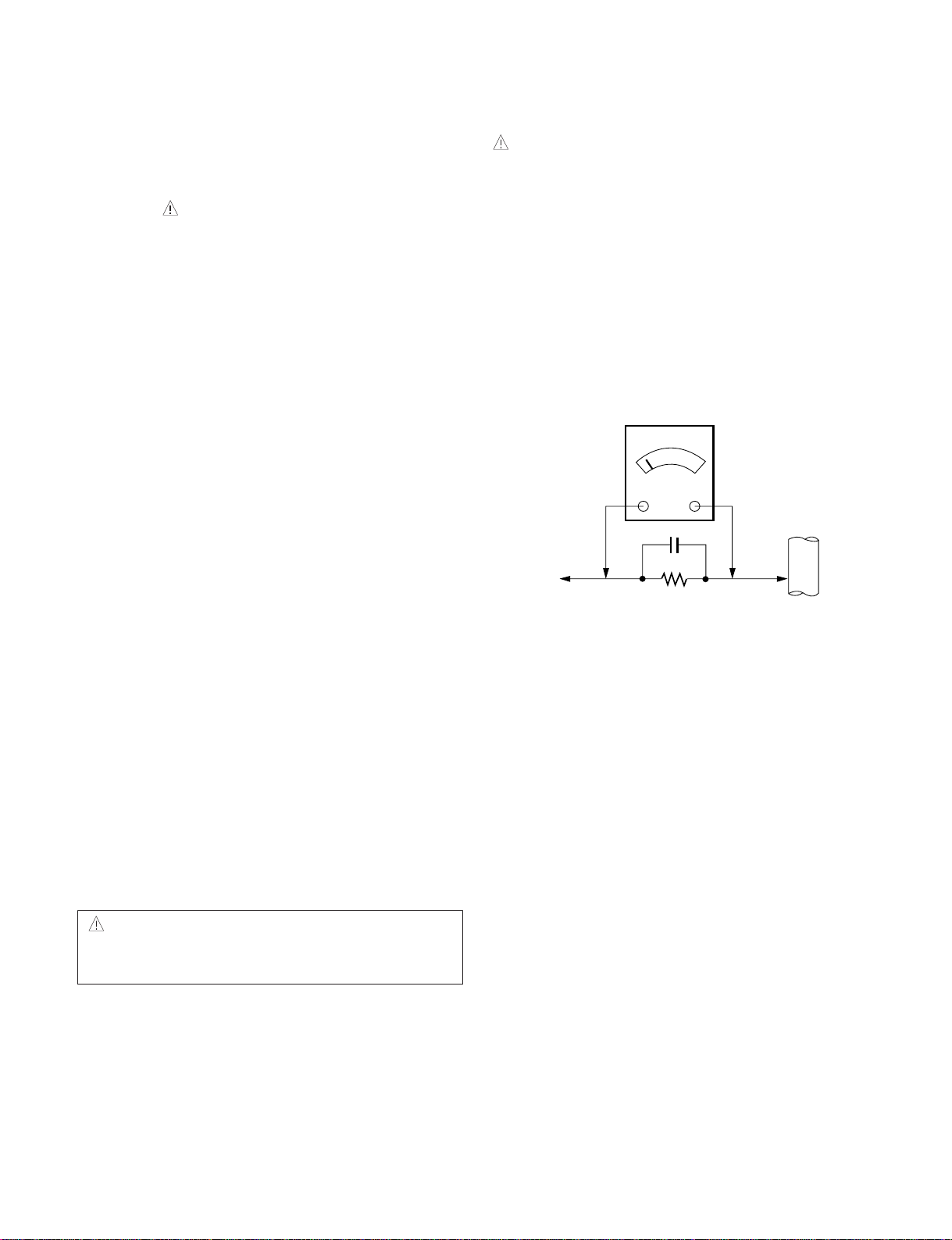
PRECAUTION
1.5 Kohm/10W
To Instrument's
exposed
METALLIC PARTS
Good Earth Ground
such as WATER PIPE,
CONDUIT etc.
AC Volt-meter
WARNING FOR THE SAFETY-RELATED COMPONENT.
• There are some special components used in LCD
monitor that are important for safety. These parts are
marked on the schematic diagram and the
replacement parts list. It is essential that these critical
parts should be replaced with the manufacturer’s
specified parts to prevent electric shock, fire or other
hazard.
• Do not modify original design without obtaining written
permission from manufacturer or you will void the
original parts and labor guarantee.
TAKE CARE DURING HANDLING THE LCD MODULE
WITH BACKLIGHT UNIT.
• Must mount the module using mounting holes arranged
in four corners.
• Do not press on the panel, edge of the frame strongly
or electric shock as this will result in damage to the
screen.
• Do not scratch or press on the panel with any sharp
objects, such as pencil or pen as this may result in
damage to the panel.
WARNING
BE CAREFUL ELECTRIC SHOCK !
• If you want to replace with the new backlight (CCFL) or
inverter circuit, must disconnect the AC adapter
because high voltage appears at inverter circuit about
650Vrms.
• Handle with care wires or connectors of the inverter
circuit. If the wires are pressed cause short and may
burn or take fire.
Leakage Current Hot Check Circuit
• Protect the module from the ESD as it may damage the
electronic circuit (C-MOS).
• Make certain that treatment person’s body are
grounded through wrist band.
• Do not leave the module in high temperature and in
areas of high humidity for a long time.
• The module not be exposed to the direct sunlight.
• Avoid contact with water as it may a short circuit within
the module.
• If the surface of panel become dirty, please wipe it off
with a softmaterial. (Cleaning with a dirty or rough cloth
may damage the panel.)
CAUTION
Please use only a plastic screwdriver to protect yourself
from shock hazard during service operation.
- 3 -
Page 7

SERVICING PRECAUTIONS
CAUTION: Before servicing receivers covered by this
service manual and its supplements and addenda, read
and follow the SAFETY PRECAUTIONS on page 3 of this
publication.
NOTE: If unforeseen circumstances create conflict
between the following servicing precautions and any of the
safety precautions on page 3 of this publication, always
follow the safety precautions. Remember: Safety First.
General Servicing Precautions
1. Always unplug the receiver AC power cord from the AC
power source before;
a. Removing or reinstalling any component, circuit
board module or any other receiver assembly.
b. Disconnecting or reconnecting any receiver electrical
plug or other electrical connection.
c. Connecting a test substitute in parallel with an
electrolytic capacitor in the receiver.
CAUTION: A wrong part substitution or incorrect
polarity installation of electrolytic capacitors may
result in an explosion hazard.
d. Discharging the picture tube anode.
2. Test high voltage only by measuring it with an
appropriate high voltage meter or other voltage
measuring device (DVM, FETVOM, etc) equipped with
a suitable high voltage probe.
Do not test high voltage by "drawing an arc".
3. Discharge the picture tube anode only by (a) first
connecting one end of an insulated clip lead to the
degaussing or kine aquadag grounding system shield
at the point where the picture tube socket ground lead
is connected, and then (b) touch the other end of the
insulated clip lead to the picture tube anode button,
using an insulating handle to avoid personal contact
with high voltage.
4. Do not spray chemicals on or near this receiver or any
of its assemblies.
5. Unless specified otherwise in this service manual,
clean electrical contacts only by applying the following
mixture to the contacts with a pipe cleaner, cottontipped stick or comparable non-abrasive applicator;
10% (by volume) Acetone and 90% (by volume)
isopropyl alcohol (90%-99% strength)
CAUTION: This is a flammable mixture.
Unless specified otherwise in this service manual,
lubrication of contacts in not required.
6. Do not defeat any plug/socket B+ voltage interlocks
with which receivers covered by this service manual
might be equipped.
7. Do not apply AC power to this instrument and/or any of
its electrical assemblies unless all solid-state device
heat sinks are correctly installed.
8. Always connect the test receiver ground lead to the
receiver chassis ground before connecting the test
receiver positive lead.
Always remove the test receiver ground lead last.
9. Use with this receiver only the test fixtures specified in
this service manual.
CAUTION: Do not connect the test fixture ground strap
to any heat sink in this receiver.
Electrostatically Sensitive (ES) Devices
Some semiconductor (solid-state) devices can be
damaged easily by static electricity. Such components
commonly are called Electrostatically Sensitive (ES)
Devices. Examples of typical ES devices are integrated
circuits and some field-effect transistors and
semiconductor "chip" components. The following
techniques should be used to help reduce the incidence of
component damage caused by static by static electricity.
1. Immediately before handling any semiconductor
component or semiconductor-equipped assembly, drain
off any electrostatic charge on your body by touching a
known earth ground. Alternatively, obtain and wear a
commercially available discharging wrist strap device,
which should be removed to prevent potential shock
reasons prior to applying power to the unit under test.
2. After removing an electrical assembly equipped with
ES devices, place the assembly on a conductive
surface such as aluminum foil, to prevent electrostatic
charge buildup or exposure of the assembly.
3. Use only a grounded-tip soldering iron to solder or
unsolder ES devices.
4. Use only an anti-static type solder removal device.
Some solder removal devices not classified as "antistatic" can generate electrical charges sufficient to
damage ES devices.
5. Do not use freon-propelled chemicals. These can
generate electrical charges sufficient to damage ES
devices.
6. Do not remove a replacement ES device from its
protective package until immediately before you are
ready to install it. (Most replacement ES devices are
packaged with leads electrically shorted together by
conductive foam, aluminum foil or comparable
conductive material).
7. Immediately before removing the protective material
from the leads of a replacement ES device, touch the
protective material to the chassis or circuit assembly
into which the device will be installed.
CAUTION: Be sure no power is applied to the chassis
or circuit, and observe all other safety precautions.
8. Minimize bodily motions when handling unpackaged
replacement ES devices. (Otherwise harmless motion
such as the brushing together of your clothes fabric or
the lifting of your foot from a carpeted floor can
generate static electricity sufficient to damage an ES
device.)
- 4 -
Page 8

General Soldering Guidelines
1. Use a grounded-tip, low-wattage soldering iron and
appropriate tip size and shape that will maintain tip
temperature within the range or 500。F to 600。F.
2. Use an appropriate gauge of RMA resin-core solder
composed of 60 parts tin/40 parts lead.
3. Keep the soldering iron tip clean and well tinned.
4. Thoroughly clean the surfaces to be soldered. Use a
mall wire-bristle (0.5 inch, or 1.25cm) brush with a
metal handle.
Do not use freon-propelled spray-on cleaners.
5. Use the following unsoldering technique
a. Allow the soldering iron tip to reach normal
temperature.
(500。F to 600。F)
b. Heat the component lead until the solder melts.
c. Quickly draw the melted solder with an anti-static,
suction-type solder removal device or with solder
braid.
CAUTION: Work quickly to avoid overheating the
circuitboard printed foil.
6. Use the following soldering technique.
a. Allow the soldering iron tip to reach a normal
temperature (500。F to 600。F)
b. First, hold the soldering iron tip and solder the strand
against the component lead until the solder melts.
c. Quickly move the soldering iron tip to the junction of
the component lead and the printed circuit foil, and
hold it there only until the solder flows onto and
around both the component lead and the foil.
CAUTION: Work quickly to avoid overheating the
circuit board printed foil.
d. Closely inspect the solder area and remove any
excess or splashed solder with a small wire-bristle
brush.
IC Remove/Replacement
Some chassis circuit boards have slotted holes (oblong)
through which the IC leads are inserted and then bent flat
against the circuit foil. When holes are the slotted type,
the following technique should be used to remove and
replace the IC. When working with boards using the
familiar round hole, use the standard technique as
outlined in paragraphs 5 and 6 above.
Removal
1. Desolder and straighten each IC lead in one operation
by gently prying up on the lead with the soldering iron
tip as the solder melts.
2. Draw away the melted solder with an anti-static
suction-type solder removal device (or with solder
braid) before removing the IC.
Replacement
1. Carefully insert the replacement IC in the circuit board.
2. Carefully bend each IC lead against the circuit foil pad
and solder it.
3. Clean the soldered areas with a small wire-bristle
brush. (It is not necessary to reapply acrylic coating to
the areas).
"Small-Signal" Discrete Transistor
Removal/Replacement
1. Remove the defective transistor by clipping its leads as
close as possible to the component body.
2. Bend into a "U" shape the end of each of three leads
remaining on the circuit board.
3. Bend into a "U" shape the replacement transistor leads.
4. Connect the replacement transistor leads to the
corresponding leads extending from the circuit board
and crimp the "U" with long nose pliers to insure metal
to metal contact then solder each connection.
Power Output, Transistor Device
Removal/Replacement
1. Heat and remove all solder from around the transistor
leads.
2. Remove the heat sink mounting screw (if so equipped).
3. Carefully remove the transistor from the heat sink of the
circuit board.
4. Insert new transistor in the circuit board.
5. Solder each transistor lead, and clip off excess lead.
6. Replace heat sink.
Diode Removal/Replacement
1. Remove defective diode by clipping its leads as close
as possible to diode body.
2. Bend the two remaining leads perpendicular y to the
circuit board.
3. Observing diode polarity, wrap each lead of the new
diode around the corresponding lead on the circuit
board.
4. Securely crimp each connection and solder it.
5. Inspect (on the circuit board copper side) the solder
joints of the two "original" leads. If they are not shiny,
reheat them and if necessary, apply additional solder.
Fuse and Conventional Resistor
Removal/Replacement
1. Clip each fuse or resistor lead at top of the circuit board
hollow stake.
2. Securely crimp the leads of replacement component
around notch at stake top.
3. Solder the connections.
CAUTION: Maintain original spacing between the
replaced component and adjacent components and the
circuit board to prevent excessive component
temperatures.
- 5 -
Page 9

Circuit Board Foil Repair
Excessive heat applied to the copper foil of any printed
circuit board will weaken the adhesive that bonds the foil
to the circuit board causing the foil to separate from or
"lift-off" the board. The following guidelines and
procedures should be followed whenever this condition is
encountered.
At IC Connections
To repair a defective copper pattern at IC connections use
the following procedure to install a jumper wire on the
copper pattern side of the circuit board. (Use this
technique only on IC connections).
1. Carefully remove the damaged copper pattern with a
sharp knife. (Remove only as much copper as
absolutely necessary).
2. carefully scratch away the solder resist and acrylic
coating (if used) from the end of the remaining copper
pattern.
3. Bend a small "U" in one end of a small gauge jumper
wire and carefully crimp it around the IC pin. Solder the
IC connection.
4. Route the jumper wire along the path of the out-away
copper pattern and let it overlap the previously scraped
end of the good copper pattern. Solder the overlapped
area and clip off any excess jumper wire.
At Other Connections
Use the following technique to repair the defective copper
pattern at connections other than IC Pins. This technique
involves the installation of a jumper wire on the
component side of the circuit board.
1. Remove the defective copper pattern with a sharp
knife.
Remove at least 1/4 inch of copper, to ensure that a
hazardous condition will not exist if the jumper wire
opens.
2. Trace along the copper pattern from both sides of the
pattern break and locate the nearest component that is
directly connected to the affected copper pattern.
3. Connect insulated 20-gauge jumper wire from the lead
of the nearest component on one side of the pattern
break to the lead of the nearest component on the
other side.
Carefully crimp and solder the connections.
CAUTION: Be sure the insulated jumper wire is
dressed so the it does not touch components or sharp
edges.
- 6 -
Page 10
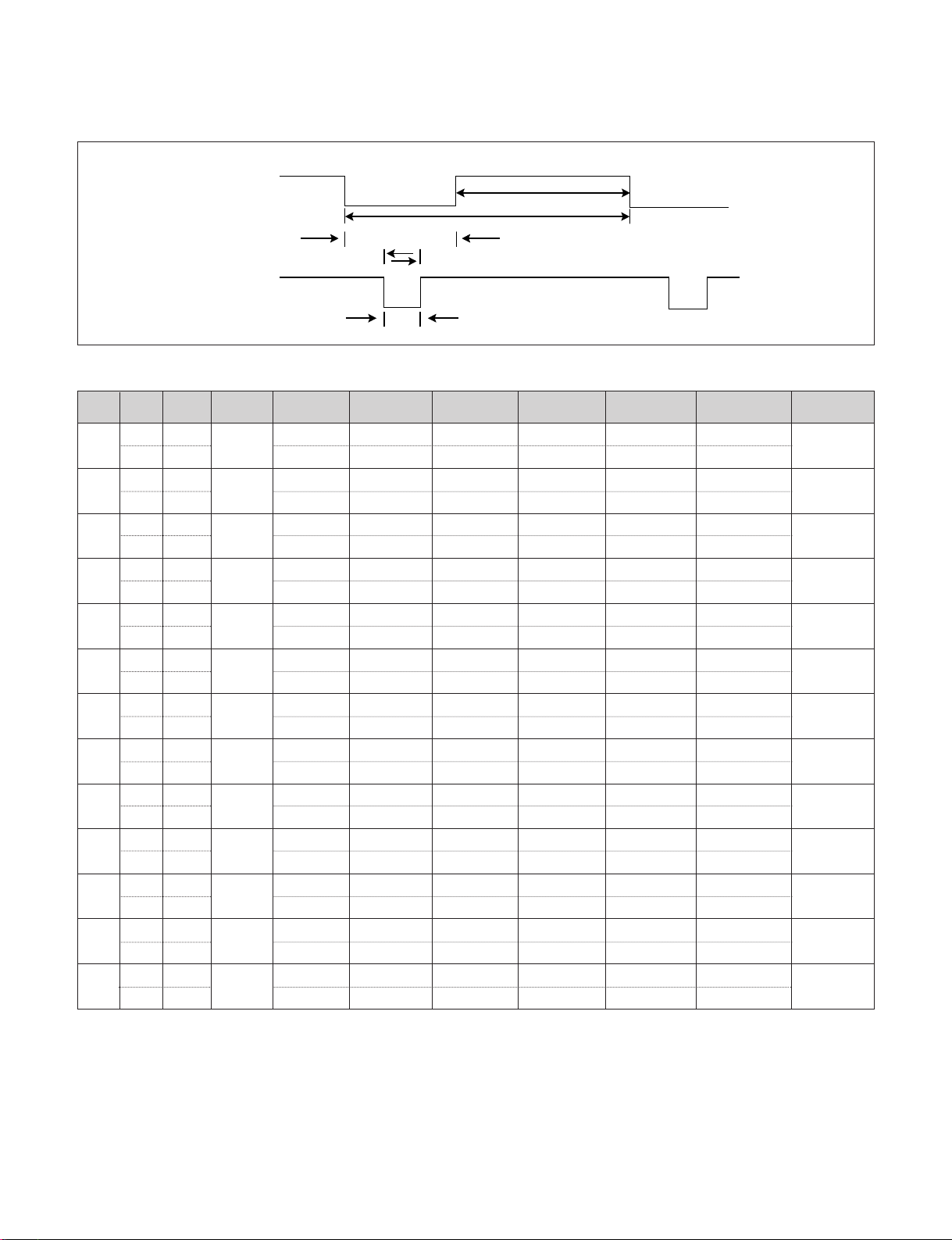
TIMING CHART
VIDEO
SYNC
B
C
E
A
D
<< Dot Clock (MHz), Horizontal Frequency (kHz), Vertical Frequency (Hz), Horizontal etc... (µs), Vertical etc... (ms) >>
Mode
1
2
3
4
5
6
7
8
9
10
11
12
13
Sync
H/V
Polarity
Sort
H + 31.469 800 640 16 96 48
V – 70.09 449 350 37 2 60
H – 31.468 900 720 18 108 54
V + 70.08 449 400 12 2 35
H – 31.469 800 640 16 96 48
V – 59.94 525 480 10 2 33
H – 37.5 840 640 16 64 120
V – 75 500 480 1 3 16
H + 37.879 1056 800 40 128 88
V + 60.317 628 600 1 4 23
H + 46.875 1056 800 16 80 160
V + 75.0 625 600 1 3 21
H+/– 49.725 1152 832 32 64 224
V+/– 74.55 667 624 1 3 39
H – 48.363 1344 1024 24 136 160
V – 60.0 806 768 3 6 29
H – 60.123 1312 1024 16 96 176
V – 75.029 800 768 1 3 28
H+/– 68.681 1456 1152 32 128 144
V+/– 75.062 915 870 3 3 39
H+/– 61.805 1504 1152 18 134 200
V+/– 65.96 937 900 2 4 31
H + 63.981 1688 1280 48 112 248
V + 60.02 1066 1024 1 3 38
H + 79.976 1688 1280 16 144 248
V + 75.035 1066 1024 1 3 38
Dot
Clock
25.175
28.321
25.175
31.5
40.0
49.5
57.283
65.0
78.75
100.0
92.978
108.0
135.0
Frequency
Total Period
(E)
Video Active Time
(A)
Front Porch
(C)
Sync Duration
(D)
Back Porch
(F)
Resolution
640x350
70Hz
720x400
70Hz
640x480
60Hz
640x480
75Hz
800x600
60Hz
800x600
75Hz
832x624
75Hz
1024x768
60Hz
1024x768
75Hz
1152x900
75Hz
1152x900
65Hz
1280x1024
60Hz
1280x1024
75Hz
- 7 -
Page 11
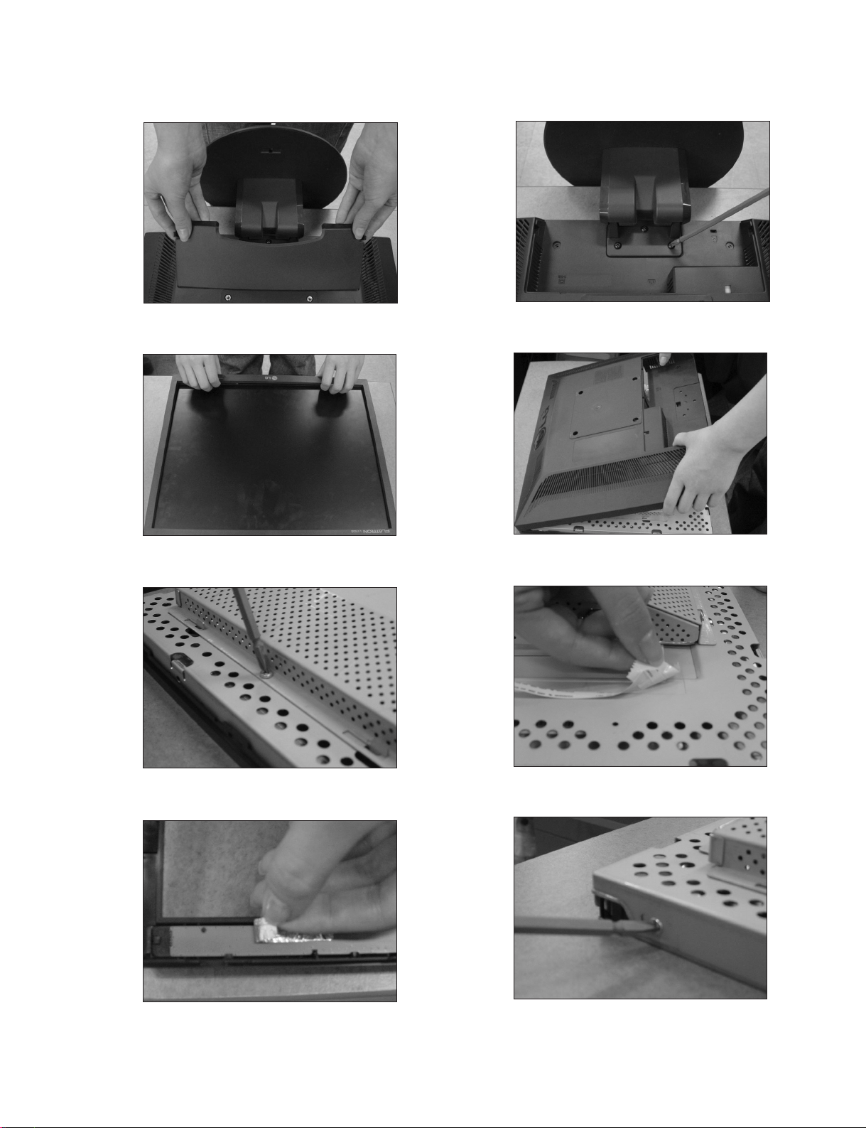
DISASSEMBLY
# 1
# 3
Disassembly Hinge Cover.
# 2
Remove the screws.
# 4
# 5
# 7
1. Pull the front cover upward.
2. Then, let the all latches are separated.
3. Put the front face down.
Remove the 6 screws from each up of metal
.
frame
Disassemble back cover
# 6
Pell off Al-tape from panel.
# 8
Remove Al-tape from control pcb fix.
Remove the 4 screws from each side of metal
frame
- 8 -
Page 12
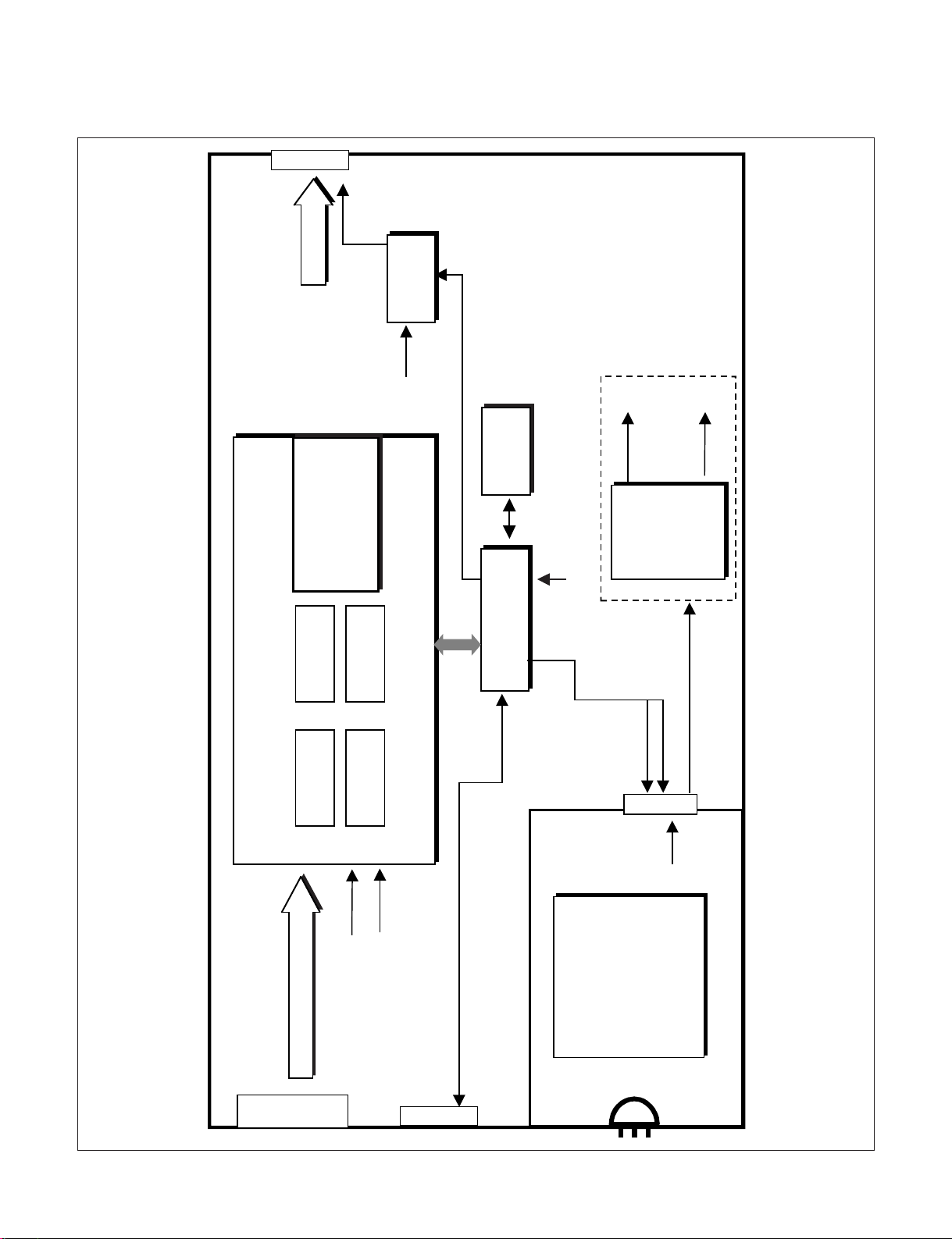
BLOCK DIAGRAM
Panel
5V
LVDS
LVDS
Transmitter
OSD
Scaling
Switch
(System)
5V
MOD-ON
EEPROM
(System)
+
MCU
5V
3.3 V
1.8 V
Regulator
gmZAN3SL
ADC
3.3 V
Analog(R/G/B)
PLL
1.8 V
D-Sub
To Key Control
- 9 -
LIPS
BRT-CTL
INV-CTL
5V
Inverter
Power +
5V
Page 13

DESCRIPTION OF BLOCK DIAGRAM
1. Video Controller Part.
This part amplifies the level of video signal for the digital conversion and converts from the analog video signal
to the digital video signal using a pixel clock.
The pixel clock for each mode is generated by the PLL.
The range of the pixel clock is from 25MHz to 135MHz.
This part consists of the Scaler, ADC, LVDS transmitter.
The Scaler gets the video signal converted analog to digital, interpolates input to 1280 X 1024 resolution signal
and outputs 8-bit R, G, B signal to transmitter.
2. Power Part.
This part consists of the one 3.3V regulator, and one 1.8V regulator to convert power which is provided 12V,
5V in Power board.
5V is provided for LCD panel and Micom.
Also, 5V is converted 3.3V by regulator and 3.3V is converted 1.8V by regulator.
Converted power is provided for IC in the main board.
3. MICOM Part.
This part consists of EEPROM IC which stores control data, Reset IC and the Micom.
The Micom distinguishes polarity and frequency of the H/V sync are supplied from signal cable.
The controlled data of each modes is stored in EEPROM.
- 10 -
Page 14
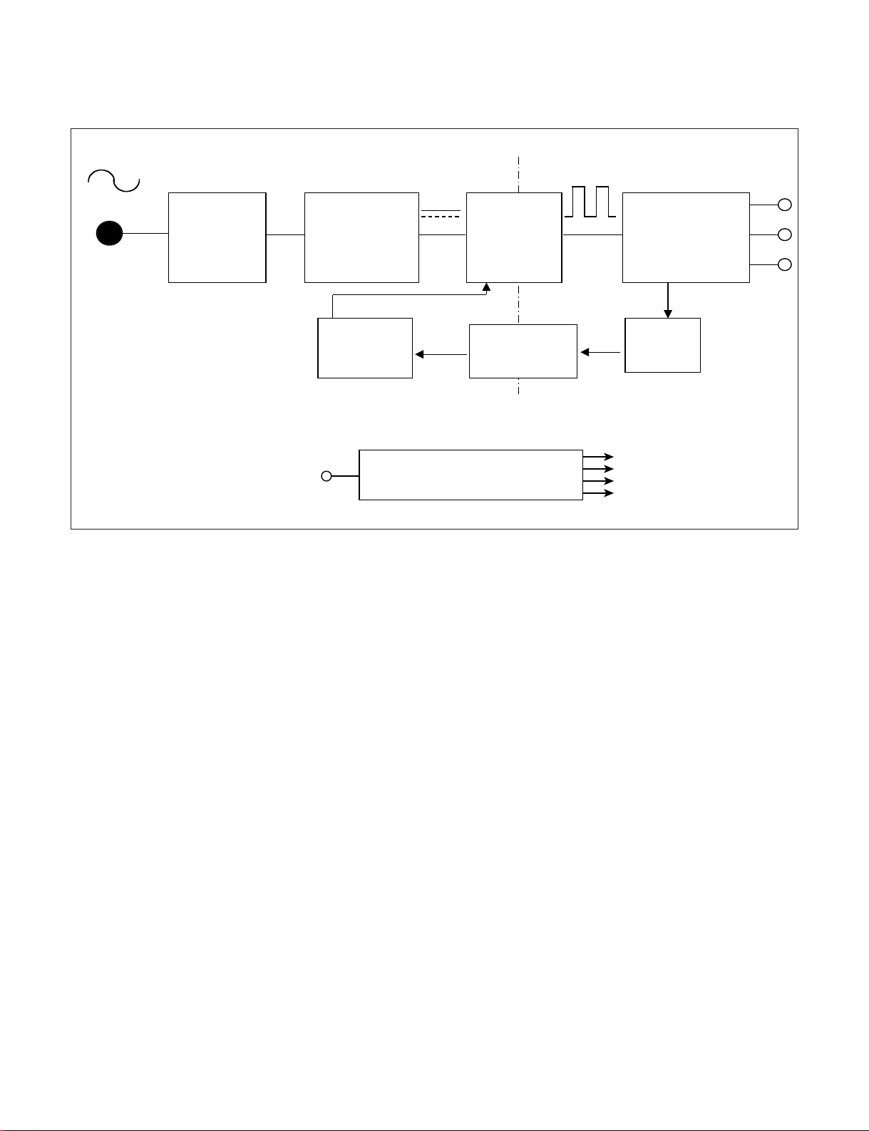
LIPS Board Block Diagram
50 ~ 60Hz
EMI
COMPONENTS
INPUT RECTIFIER
AND FILTER
HVDC
ENERGY
TRANSFER
100KHz
OUTPUT RECTIFIER
AND FILTER
LINE
100 ~ 240V
PWM CONTROL
CIRCUIT
PHOTO
ISOLATION
-COUPLER
SIGNAL
COLLECT-
ON
PRIMARY SECONDARY
12V
INVERTER CIRCUIT
Operation description_LIPS
1. EMI components.
This part contains of EMI components to comply with global marketing EMI standards like FCC, VCCI CISPR, the
circuit included a line-filter, across line capacitor and of course the primary protection fuse.
High Voltage output
12V
5V
GND
2. Input rectifier and filter.
This part function is for transfer the input AC voltage to a DC voltage through a bridge rectifier and a bulk capacitor.
3. Energy Transfer.
This part function is transfer the primary energy to secondary through a power transformer.
4. Output rectifier and filter.
This part function is to make a pulse width modulation control and to provide the driver signal to power switch, to
adjust the duty cycle during different AC input and output loading condition to achive the dc output stablize, and also
the over power protection is also monitor by this part.
5. Photo-Coupler isolation.
This part function is to feed back the dc output changing status through a photo transistor to primary controller to
achieve the stabilized dc output voltage.
6. Signal collection.
This part function is to collect the any change from the dc output and feed back to the primary through photo
transistor.
- 11 -
Page 15
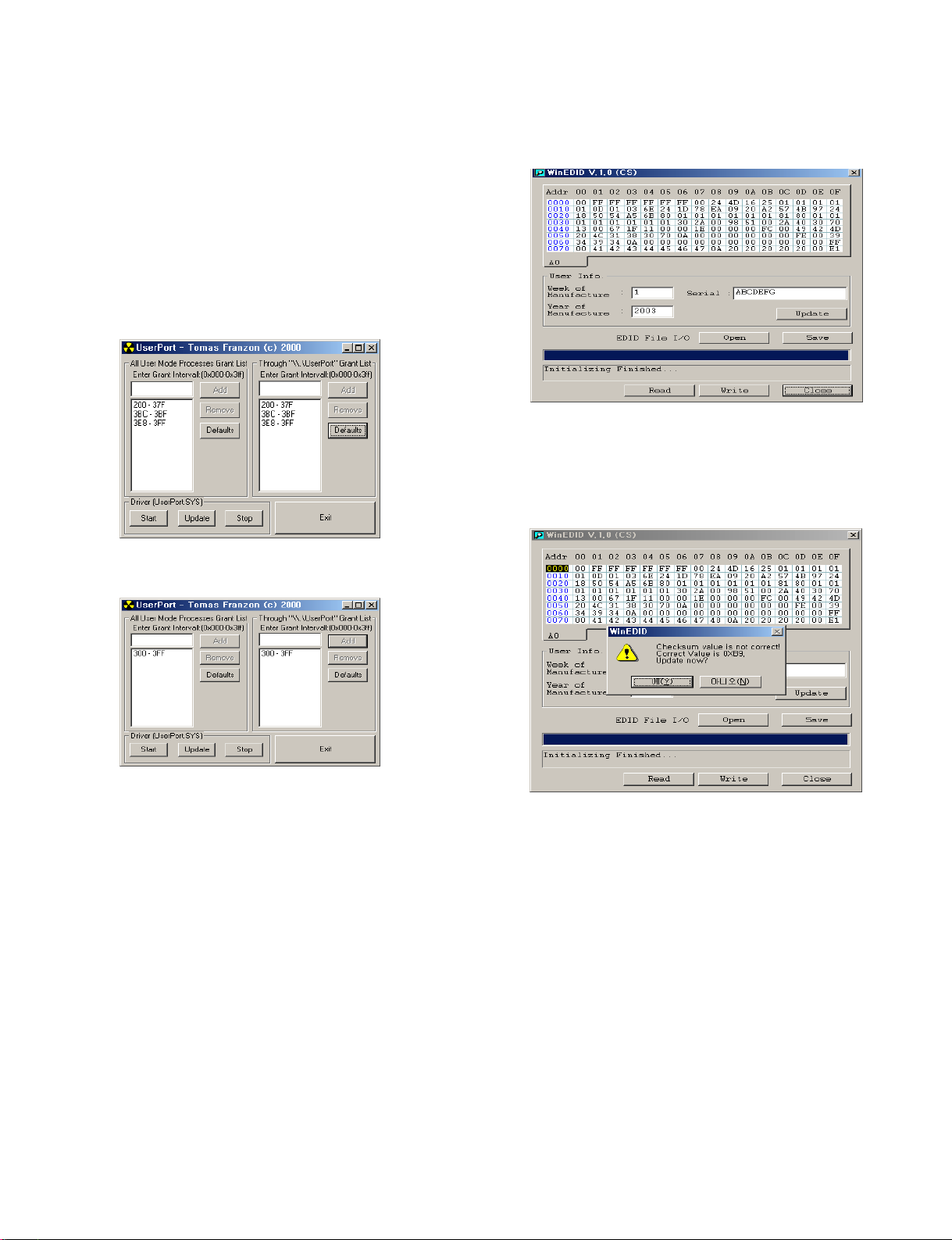
ADJUSTMENT
Windows EDID V1.0 User Manual
Operating System: MS Windows 98, 2000, XP
Port Setup: Windows 98 => Don’t need setup
Windows 2000, XP => Need to Port Setup.
This program is available to LCD Monitor only.
1. Port Setup
a) Copy “UserPort.sys” file to
“c:\WINNT\system32\drivers” folder
b) Run Userport.exe
c) Remove all default number
d) Add 300-3FF
2. EDID Read & Write
1) Run WinEDID.exe
2) Edit Week of Manufacture, Year of Manufacture,
Serial Number
a) Input User Info Data
b) Click “Update” button
c) Click “ Write” button
e) Click Start button.
f) Click Exit button.
- 12 -
Page 16
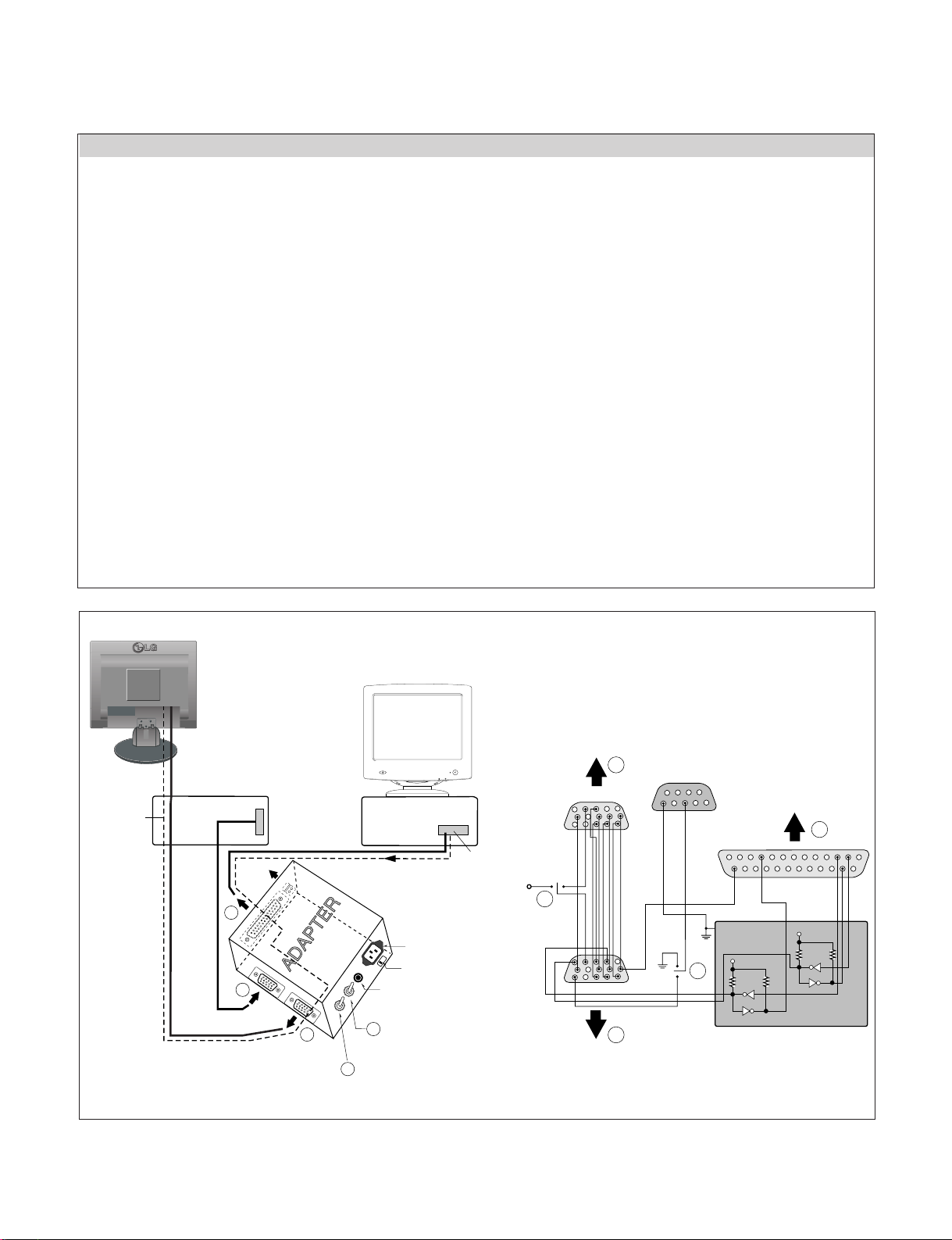
220
IBM
Compatible PC
Video Signal
Generator
PARALLEL PORT
Power inlet (required)
Power LED
ST Switch
Power Select Switch
(110V/220V)
Control Line
Not used
RS232C
PARALLEL
V-SYNC
POWER
ST
VGS
MONITOR
E
E
V-Sync On/Off Switch
(Switch must be ON.)
F
F
A
A
B
B
C
C
15
10
5
5
69
1
1
1
14
13
25
6
5V
5V
5V
4.7K
4.7K
4.7K
74LS06
74LS06
OFF ON
OFF
ON
11
SERVICE OSD
1) Turn off the power switch at the front side of the display.
2) Wait for about 5 seconds and press MENU, POWER switch with 1 second interval.
3) The SVC OSD menu contains additional menus that the User OSD menu as described below.
a) Auto Color : W/B balance and Automatically sets the gain and offset value.
b) NVRAM INIT : EEPROM initialize.(24C08)
c) CLEAR ETI : To initialize using time.
d) AGING : Select Aging mode(on/off).
e) R/G/B-9300K : Allows you to set the R/G/B-9300K value manually.
f) R/G/B-6500K : Allows you to set the R/G/B-6500K value manually.
g) R/G/B-Offset : Allows you to set the R/G/B-Offset value manually.(Analog Only)
h) R/G/B-Gain : Allows you to set the R/G/B-Gain value manually.(Analog Only)
i) MODULE : To select applied module.
Figure 1. Cable Connection
- 13 -
Page 17
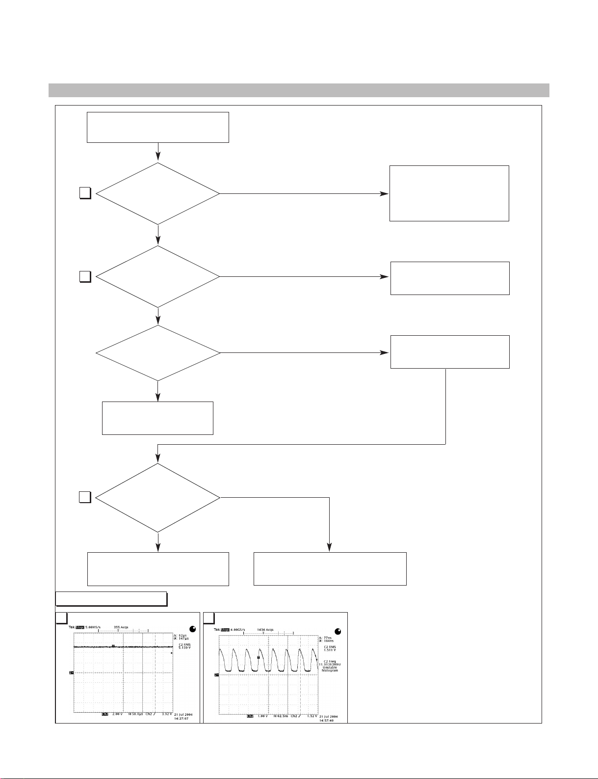
NO POWER
(POWER INDICATOR OFF)
TROUBLESHOOTING GUIDE
1. NO POWER
CHECK J705 VOLTAGE
1
PIN5, PIN6 (5V)?
CHECK
1
U801 PIN 1& U803
PIN 3 VOLTAGE
(5V) ?
CHECK
Q803 PIN 3(3.3V) &
U803 PIN 4 (1.8V)?
CHECK KEY CONTROL
CONNECTOR ROUTINE
YES
YES
YES
NO
NO
NO
CHECK POWER BOARD,
AND FIND OUT A SHORT
POINT AS OPENING
EACH POWER LINE
CHECK U801.
CHECK 5VR LINE
(OPEN CHECK)
NO PROBLEM
IS U201
2
VOLTAGE REPEATED
CHECK IIC LINE CONNECTION
PIN88
AS PULSE
SHAPE ?
YES
(U501, U502)
Waveforms
1 2
J705-#5, 6 / U801-#1/U803-#3 U201-#88
NO
CHECK U201 VCC, XTAL, RESET
- 14 -
Page 18
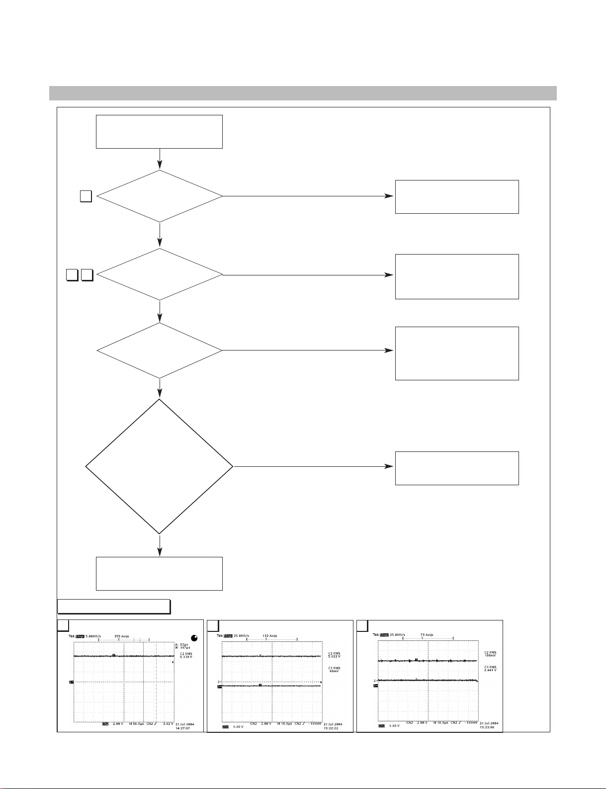
2. NO RASTER (OSD IS NOT DISPLAYED) – LIPS
NO RASTER
(OSD IS NOT DISPLAYED)
1
PIN5, PIN 6
5V?
J705
3 4
J705 PIN9
2.5V?
J705 PIN10
5V?
CHECK
PULSE AS
CONTACTING SCOPE
PROBE TO CAUTION LABEL.
(CONTACT PROBE TO
CAUTION LABEL.
CAN YOU SEE PULSE
AT YOUR
SCOPE?
YES
YES
YES
NO
NO
NO
NO
CHECK LIPS
CHECK MICOM INV
ON/OFF PORT.
(U501 PIN9)
1. CONFIRM BRIGHTNESS
OSD CONTRL STATE.
2. CHECK MICOM DIM-ADJ
PORT(U501 PIN41)
LIPS
REPLACE CCFL LAMP
IN THE LCD MODULE
Waveforms
1
J705-#5, 6 / U801-#1/U803-#3
YES
3 4
J705-#9 J705-#9
Inverter Off
Micom Port check
J705 Inverter output
- 15 -
Inverter On
Micom Port check
J705 Inverter output
Page 19
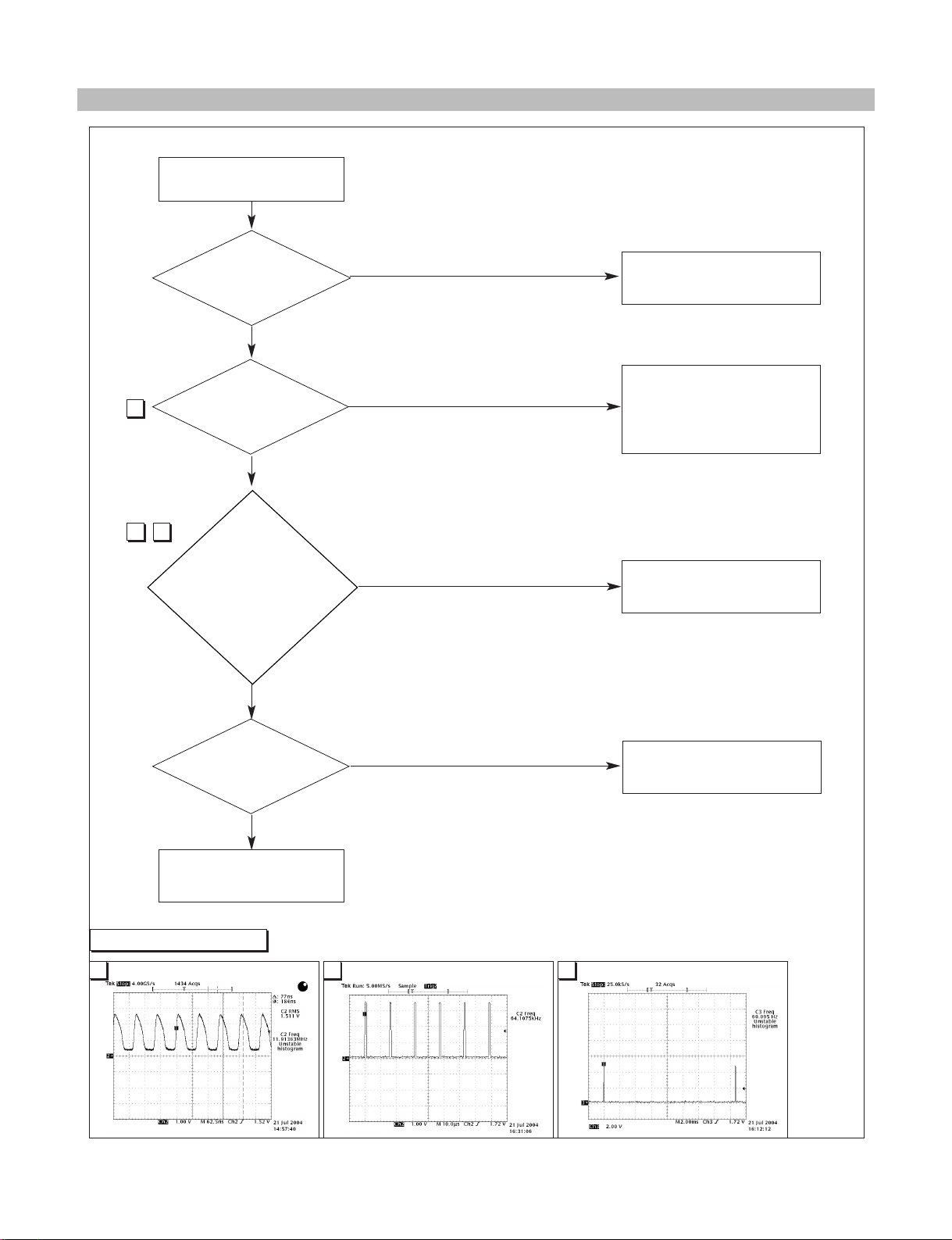
3. NO RASTER (OSD IS NOT DISPLAYED) – gmZAN3SL
NO RASTER
(OSD IS NOT DISPLAYED)
U201
POWER PINS
3.3V?
U201
2
PIN88
OSCILLATE AS
12MHZ?
5 6
U501
PIN43 IS 64KHz H-SYNC?
PIN44 IS 60Hz V-SYNC?
IS PULSE APPEARED
AT SIGNAL PINS?
YES
YES
YES
NO
NO
NO
CHECK U803, U801
1. CHECK PIN88
SOLDERINGCONDITION
2. CHECK X501
3. TROUBLE IN U201
CHECK CONNECTION
LINE FROM U201 TO U501
TROUBLE IN CABLE
OR LCD MODULE
Waveforms
U501 PIN8
5V?
YES
52
U501-#43
NO
- 16 -
CHECK 5VR LINE
6
U501-#44U201-#88
Page 20
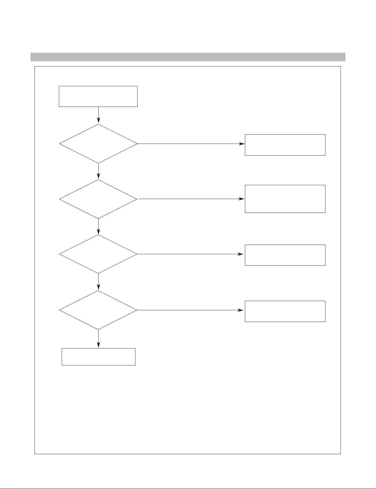
4. NO RASTER (OSD IS DISPLAYED) – gmZAN3SL
NO RASTER
(OSD IS DISPLAYED)
U201
POWER PIN99(1.8V)
PIN33(3.3V)?
YES
CHECK
R,G,B INPUT?
U201 PIN 70,74,77
YES
CHECK
H-SYNC INPUT
U201 PIN 95?
YES
CHECK
V-SYNC INPUT
U201 PIN 96?
NO
NO
NO
NO
CHECK U803, U801
1. CHECK PC
2. CHECK SIGNAL CABLE
& D-SUB CONNECTOR LINE
CHECK H-SYNC LINE
(D-SUB→U501→U201 PIN95)
CHECK V-SYNC LINE
(D-SUB→U501→U201 PIN96)
YES
TROUBLE IN
LCD MODULE
- 17 -
Page 21
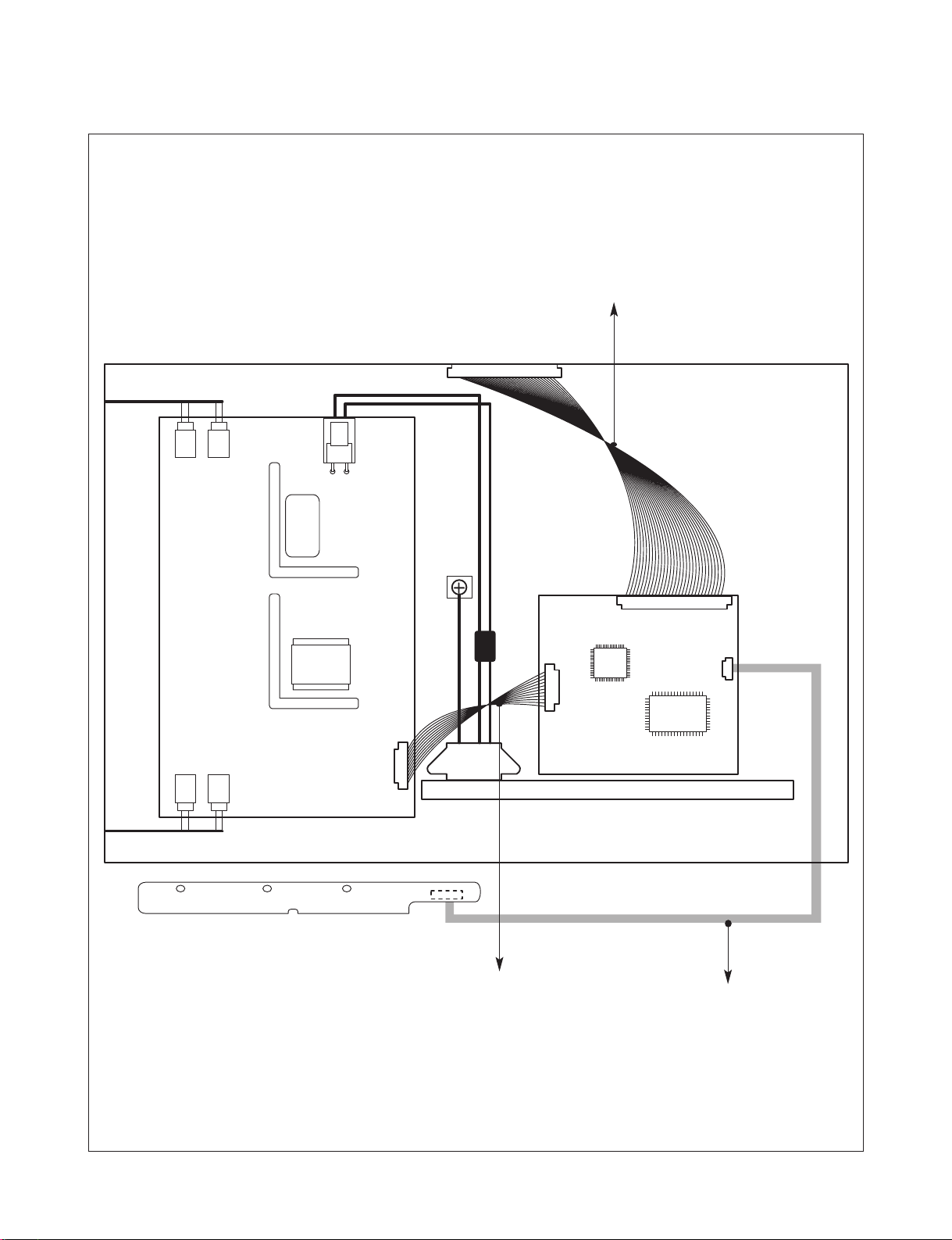
WIRING DIAGRAM
Connector Ass’y P/N
or 6631T11020W
6631T11012W
Connector Ass’y P/N:
6631T20023A
or
6631T20034M
- 18 -
Connector Ass’y P/N:
6631T11017X-L1750S
6631T11017Y-L1950S
Page 22
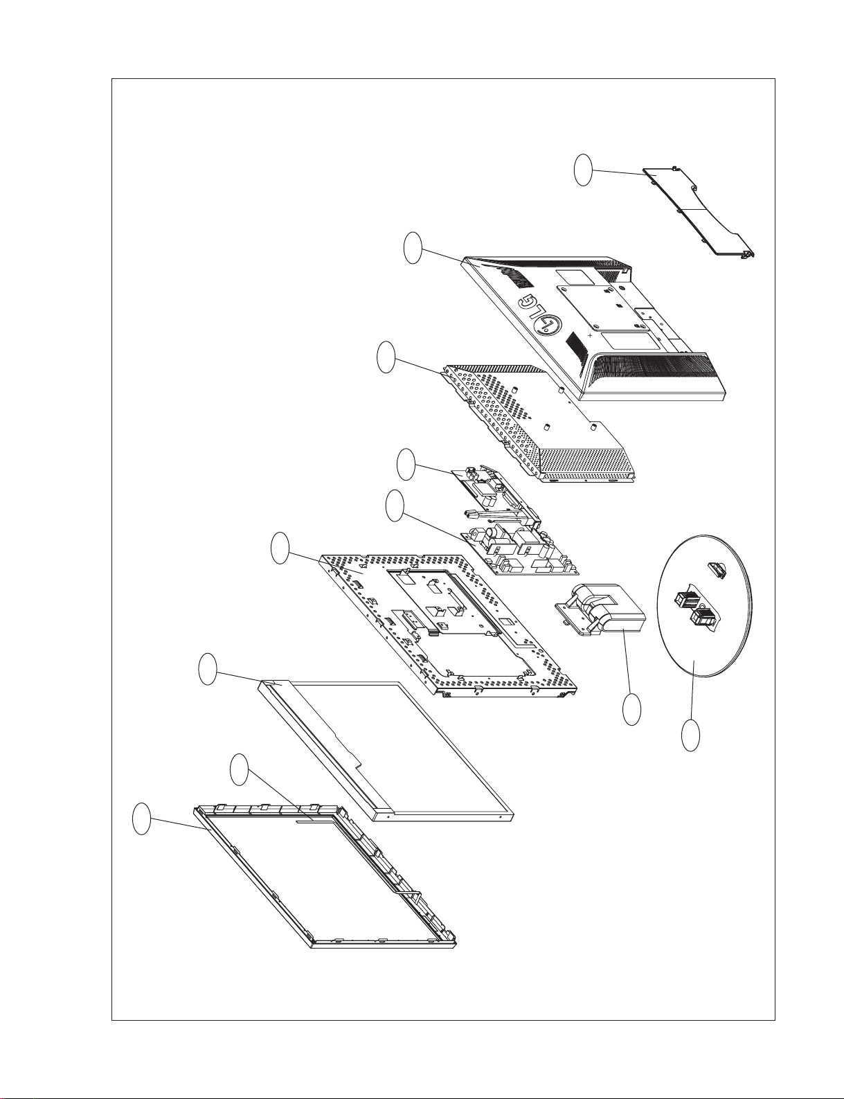
060
100
030
090
080
070
EXPLODED VIEW
020
010
040
050
110
- 19 -
Page 23
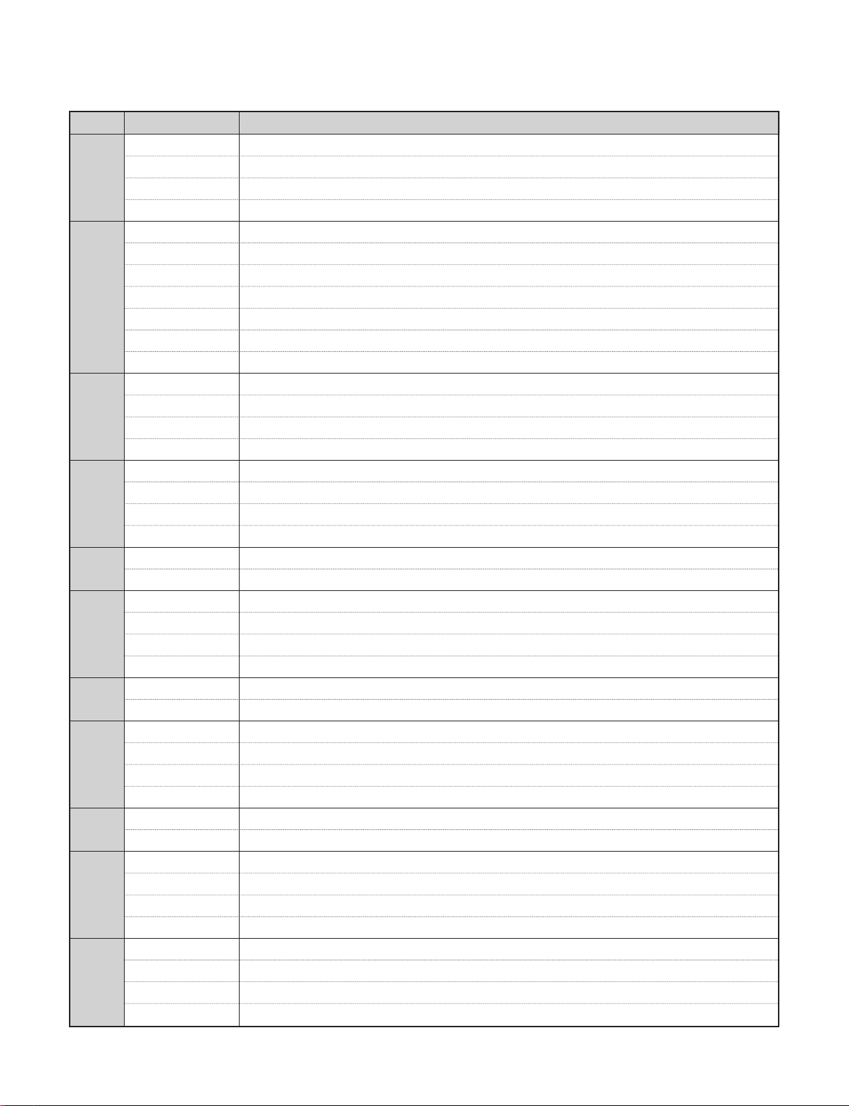
EXPLODED VIEW PARTS LIST
Ref. No.
010
020
030
040
050
060
070
080
090
100
110
Part No.
3091TKL143N CABINET ASSEMBLY, L1750S BRAND L122 SILVER PC+ABS,89483 TCO03 US-VER
3091TKL143R CABINET ASSEMBLY, L1750S BRAND L122 SILVER PC+ABS TCO03+12MS FLATRON N-C/SKD
3091TKL144N CABINET ASSEMBLY, L1950S BRAND L123 SILVER PC+ABS,89483 TCO03
3091TKL144Q CABINET ASSEMBLY, L1950S BRAND L123 SILVER PC+ABS 12MS+TCO03, US N-C/SKD
6304FLP110B
or 6304FLP086A
or 6304FLP194A
or 6304FLP110A
or 6304FLP160A
6304FLP142A
or 6304FLP184A
3809TKL100E BACK COVER ASSEMBLY, L1750S L100 PC+ABS 9930(BK) US-VER
3809TKL100G BACK COVER ASSEMBLY, L1750S L100 PC+ABS 9930(BK) ANALOG US-VER E-C/SKD
3809TKL101E BACK COVER ASSEMBLY, L1950S L101 BRAND PC+ABS 9930(BK) US-VER
3809TKL101F BACK COVER ASSEMBLY, L1950S L101 BRAND PC+ABS 9930(BK) US-VER E-C/SKD
3043TKK227A TILT SWIVEL ASSEMBLY, L1750S - TILT STAND BODY
3043TKK227C TILT SWIVEL ASSEMBLY, L1750S - TILT STAND BODY A-C/SKD
3043TKK227B TILT SWIVEL ASSEMBLY, L1950S - TILT STAND BODY.
3043TKK227D TILT SWIVEL ASSEMBLY, L1950S - TILT STAND BODY B-C/SKD
3043TKK228A TILT SWIVEL ASSEMBLY, L1750S - TILT STAND BASE
3043TKK228B TILT SWIVEL ASSEMBLY, LX 50S - TILT STAND BASE A-C/SKD
4951TKS199A METAL ASSEMBLY, FRAME MAIN L1750 LPL-A5 KUMI
4951TKS199B METAL ASSEMBLY, FRAME MAIN L1750 A-C/SKD
4951TKS200A METAL ASSEMBLY, FRAME MAIN L1950 LPL-E03 TN/AUO-EN04-V2 KUMI
4951TKS200C METAL ASSEMBLY, FRAME MAIN L1950 LPL-E03 TN/AUO-EN04-V2 A-C/SKD
6871TPT282C
6871TPT282Q
3313TL7087A MAIN TOTAL ASSEMBLY, L1750SN LPL ZAN3SL BRAND CL-66
3313TL7087E MAIN TOTAL ASSEMBLY, L1750SN LPL ZAN3SL MX C/SKD BRAND CL-82 LF
3313TL9078A MAIN TOTAL ASSEMBLY, L1950SN LPL ZAN3SL BRAND CL-66
3313TL9078E MAIN TOTAL ASSEMBLY, L1950SN LPL ZAN3SL MX C/SKD BRAND CL-82 LF
4951TKS203A METAL ASSEMBLY, REAR SHIELD LX50 KUMI
4951TKS203B METAL ASSEMBLY, REAR SHIELD LX50 KUMI A-C/SKD
3550TKK740A COVER, L1750 BACK DOOR BRAND
3550TKK740B COVER, L1750 BACK DOOR BRAND A-C/SKD
3550TKK741A COVER, L1950 BACK DOOR BRAND
3550TKK741B COVER, L1950 BACK DOOR BRAND A-C/SKD
6871TST798A PWB(PCB) ASSEMBLY,SUB, L1750 CONTROL TOTAL BRAND KEY
6871TST798C PWB(PCB) ASSEMBLY,SUB, L1750 CONTROL TOTAL BRAND MX C/SKD LF
6871TST911A PWB(PCB) ASSEMBLY,SUB, L1950 CONTROL TOTAL BRAND KEY
6871TST911C PWB(PCB) ASSEMBLY,SUB, L1950 CONTROL TOTAL BRAND MX C/SKD LF
LCD(LIQUID CRYSTAL DISPLAY), LM170E01-A5N5 LG PHILPS TFT COLOR PART NUMBER CHANGE FOR COST COMPENSATION
LCD(LIQUID CRYSTAL DISPLAY), LM170E01-A5K6 LG PHILPS TFT COLOR LVDS SXGA OKI GATE D-IC
LCD(LIQUID CRYSTAL DISPLAY), LM170E01-A5K2 LG PHILPS TFT COLOR TI D-IC,250NITS,SXGA,LVDS
LCD(LIQUID CRYSTAL DISPLAY), LM170E01-A5N5 LG PHILPS TFT COLOR LPL NJ,250NITS,SXGA,LVDS
LCD(LIQUID CRYSTAL DISPLAY), LM170E01-A5KS LG PHILPS TFT COLOR NEC D-IC,250NITS,SXGA,LVDS
LCD(LIQUID CRYSTAL DISPLAY), LM190E03-B4K1 LG PHILPS TFT COLOR 20T,TN,250NITS,SXGA,LVDS
LCD(LIQUID CRYSTAL DISPLAY), LM190E03-B4N2 LG PHILPS TFT COLOR B4K1 LPL NJ,20T,TN,250NITS,SXGA,LVDS
PWB(PCB) ASSEMBLY,POWER, M-CHASSIS 1720 DOCKING,2PIN,450V POWER TOTAL LIEN CHANG PB FREE-L1750S
PWB(PCB) ASSEMBLY,POWER, M-CHASSIS 19INCH TN & 1720 DOCKING,2PIN,450V POWER TOTAL LIEN CHANG PB FREE & ANALOG-L1950S
Description
- 20 -
Page 24
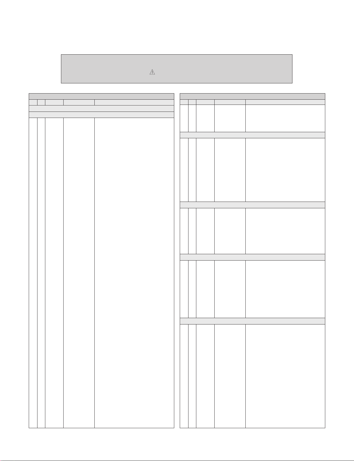
REPLACEMENT PARTS LIST
CAUTION: BEFORE REPLACING ANY OF THESE COMPONENTS,
READ CAREFULLY THE SAFETY PRECAUTIONS IN THIS MANUAL.
* NOTE : S SAFETY Mark
AL ALTERNATIVE PARTS
DATE: 2004. 12. 17.
*S *AL LOC. NO. PART NO. DESCRIPTION / SPECIFICATION
MAIN BOARD
CAPACITORS
C204 0CK103CK51A 0.01UF 1608 50V 10% R/TP B(Y
C205 0CK103CK51A 0.01UF 1608 50V 10% R/TP B(Y
C206 0CK103CK51A 0.01UF 1608 50V 10% R/TP B(Y
C207 0CK103CK51A 0.01UF 1608 50V 10% R/TP B(Y
C208 0CK103CK51A 0.01UF 1608 50V 10% R/TP B(Y
C210 0CK103CK51A 0.01UF 1608 50V 10% R/TP B(Y
C213 0CK103CK51A 0.01UF 1608 50V 10% R/TP B(Y
C214 0CK103CK51A 0.01UF 1608 50V 10% R/TP B(Y
C215 0CK103CK51A 0.01UF 1608 50V 10% R/TP B(Y
C216 0CK103CK51A 0.01UF 1608 50V 10% R/TP B(Y
C217 0CK103CK51A 0.01UF 1608 50V 10% R/TP B(Y
C218 0CK103CK51A 0.01UF 1608 50V 10% R/TP B(Y
C219 0CK103CK51A 0.01UF 1608 50V 10% R/TP B(Y
C220 0CK103CK51A 0.01UF 1608 50V 10% R/TP B(Y
C221 0CK103CK51A 0.01UF 1608 50V 10% R/TP B(Y
C222 0CK103CK51A 0.01UF 1608 50V 10% R/TP B(Y
C223 0CK103CK51A 0.01UF 1608 50V 10% R/TP B(Y
C224 0CK103CK51A 0.01UF 1608 50V 10% R/TP B(Y
C225 0CK103CK51A 0.01UF 1608 50V 10% R/TP B(Y
C226 0CK103CK51A 0.01UF 1608 50V 10% R/TP B(Y
C227 0CK103CK51A 0.01UF 1608 50V 10% R/TP B(Y
C231 0CK103CK51A 0.01UF 1608 50V 10% R/TP B(Y
C232 0CK103CK51A 0.01UF 1608 50V 10% R/TP B(Y
C233 0CK103CK51A 0.01UF 1608 50V 10% R/TP B(Y
C234 0CK103CK51A 0.01UF 1608 50V 10% R/TP B(Y
C503 0CK103CK51A 0.01UF 1608 50V 10% R/TP B(Y
C504 0CE106CK610 "10UF SHL,SD 50V 20% BULK FL"
C506 0CC030CK01A 3PF 1608 50V 0.25 PF R/TP NP
C507 0CC180CK41A 18PF 1608 50V 5% R/TP NP0
C508 0CK103CK51A 0.01UF 1608 50V 10% R/TP B(Y
C701 0CK105CD56A 1UF 1608 10V 10% R/TP X7R
C708 0CK103CK51A 0.01UF 1608 50V 10% R/TP B(Y
C709 0CK103CK51A 0.01UF 1608 50V 10% R/TP B(Y
C717 0CC101CK41A 100PF 1608 50V 5% R/TP NP0
C718 0CC101CK41A 100PF 1608 50V 5% R/TP NP0
C720 0CC680CK41A 68PF 1608 50V 5% R/TP NP0
C721 0CC680CK41A 68PF 1608 50V 5% R/TP NP0
C727 0CK105CD56A 1UF 1608 10V 10% R/TP X7R
C732 0CK103CK51A 0.01UF 1608 50V 10% R/TP B(Y
C733 0CK104CK56A 0.1UF 1608 50V 10% R/TP X7R
C734 0CK104CK56A 0.1UF 1608 50V 10% R/TP X7R
C735 0CK104CK56A 0.1UF 1608 50V 10% R/TP X7R
C801 0CK103CK51A 0.01UF 1608 50V 10% R/TP B(Y
C803 0CK104CK56A 0.1UF 1608 50V 10% R/TP X7R-L1750S
C819 0CK103CK51A 0.01UF 1608 50V 10% R/TP B(Y
C820 0CE107EF610 "100UF KMG,RD 16V 20% FL BULK"
C820 0CE107EF628 "100UF KMG,RD 16V 20% FM2.5 T"-C/SKD
C821 0CK103CK51A 0.01UF 1608 50V 10% R/TP B(Y
C829 0CK103CK51A 0.01UF 1608 50V 10% R/TP B(Y
C831 0CE107EF610 "100UF KMG,RD 16V 20% FL BULK"
C831 0CE107EF628 "100UF KMG,RD 16V 20% FM2.5 T"-C/SKD
C832 0CE107EF610 "100UF KMG,RD 16V 20% FL BULK"-C/SKD
DATE: 2004. 12. 17.
*S *AL LOC. NO. PART NO. DESCRIPTION / SPECIFICATION
C832 0CE107EF628 "100UF KMG,RD 16V 20% FM2.5 T"
C833 0CK105CD56A 1UF 1608 10V 10% R/TP X7R-L1950S
C834 0CC102CK41A 1000PF 1608 50V 5% R/TP NP0-L1950S
DIODEs
D701 0DS226009AA KDS226 TP KEC SOT-23 80V 30
D702 0DS226009AA KDS226 TP KEC SOT-23 80V 30
D706 0DS226009AA KDS226 TP KEC SOT-23 80V 30
ZD701 0DZKE00138A KDZ5.6V KEC R/TP USC 0.2W 5.
ZD702 0DZKE00138A KDZ5.6V KEC R/TP USC 0.2W 5.
ZD703 0DZKE00138A KDZ5.6V KEC R/TP USC 0.2W 5.
ZD704 0DZKE00138A KDZ5.6V KEC R/TP USC 0.2W 5.
ZD705 0DZKE00138A KDZ5.6V KEC R/TP USC 0.2W 5.
ZD711 0DZKE00138A KDZ5.6V KEC R/TP USC 0.2W 5.
ICs
U201 0IPRPGN016B "GMZAN3SL-BD-LF GENESIS 128P,"
U501 0IZZTSZ594A L1750SN ZAN3SL MICOM ASSY -L1750S
U502 0ISG240860B "M24C08WMN6T(P),LF SGS-THOMSO"
U801 0IPMGKE011A KIA78D33F KEC DPAK R/TP 3.3V
U803 0IPMGSG019A "LD1117S18TR,LF STM SOT223 R/"
Q502 0IKE704200H KIA7042AP TO-92 TP 4.2 VOLT
TRANSISTOR
Q503 0TR390409AE FAIRCHILD KST3904(LGEMTF) TP
Q504 0TR390409AE FAIRCHILD KST3904(LGEMTF) TP
Q505 0TR390409AE FAIRCHILD KST3904(LGEMTF) TP
Q703 0TR390609FA KST3906-MTF TP SAMSUNG SOT2
Q704 0TR390609FA KST3906-MTF TP SAMSUNG SOT2
Q803 0TR127309AA KTA1273-Y(KTA966A) TP KEC TO-L1750S
Q804 0TR390409AE FAIRCHILD KST3904(LGEMTF) TP-L1750S
U802 0TFVI80023A VISHAY SI3865DV R/TP TSOP-6-L1950S
RESISTORs
R201 0RJ1000D677 100 OHM 1/10 W 5% 1608 R/TP
R202 0RJ1000D677 100 OHM 1/10 W 5% 1608 R/TP
R203 0RJ1000D677 100 OHM 1/10 W 5% 1608 R/TP
R208 0RJ1200D677 120 OHM 1/10 W 5% 1608 R/TP
R209 0RJ1200D677 120 OHM 1/10 W 5% 1608 R/TP
R210 0RJ1200D677 120 OHM 1/10 W 5% 1608 R/TP
R211 0RJ1000D677 100 OHM 1/10 W 5% 1608 R/TP
R213 0RJ0000D677 0 OHM 1/10 W 5% 1608 R/TP
R214 0RJ0000D677 0 OHM 1/10 W 5% 1608 R/TP
R220 0RJ0000D677 0 OHM 1/10 W 5% 1608 R/TP
R221 0RJ0000D677 0 OHM 1/10 W 5% 1608 R/TP
R222 0RJ1004D677 1000000 OHM 1/10 W 5% 1608 R
R506 0RJ4701D677 4.7K OHM 1/10 W 5% 1608 R/TP
R508 0RJ4701D677 4.7K OHM 1/10 W 5% 1608 R/TP
R514 0RJ4701D677 4.7K OHM 1/10 W 5% 1608 R/TP
R515 0RJ4701D677 4.7K OHM 1/10 W 5% 1608 R/TP
- 21 -
Page 25
DATE: 2004. 12. 17.
*S *AL LOC. NO. PART NO. DESCRIPTION / SPECIFICATION
DATE: 2004. 12. 17.
*S *AL LOC. NO. PART NO. DESCRIPTION / SPECIFICATION
R516 0RJ4701D677 4.7K OHM 1/10 W 5% 1608 R/TP
R518 0RJ4701D677 4.7K OHM 1/10 W 5% 1608 R/TP
R520 0RJ4701D677 4.7K OHM 1/10 W 5% 1608 R/TP
R521 0RJ4701D677 4.7K OHM 1/10 W 5% 1608 R/TP
R522 0RJ4701D677 4.7K OHM 1/10 W 5% 1608 R/TP
R523 0RJ4701D677 4.7K OHM 1/10 W 5% 1608 R/TP
R534 0RJ0000D677 0 OHM 1/10 W 5% 1608 R/TP
R535 0RJ3301D677 3.3K OHM 1/10 W 5% 1608 R/TP
R537 0RJ3301D677 3.3K OHM 1/10 W 5% 1608 R/TP
R541 0RJ1000D677 100 OHM 1/10 W 5% 1608 R/TP
R542 0RJ1000D677 100 OHM 1/10 W 5% 1608 R/TP
R543 0RJ4701D677 4.7K OHM 1/10 W 5% 1608 R/TP
R544 0RJ4701D677 4.7K OHM 1/10 W 5% 1608 R/TP
R545 0RJ4700D677 470 OHM 1/10 W 5% 1608 R/TP
R547 0RJ4700D677 470 OHM 1/10 W 5% 1608 R/TP
R548 0RJ0332D677 33 OHM 1/10 W 5% 1608 R/TP
R549 0RJ0332D677 33 OHM 1/10 W 5% 1608 R/TP
R555 0RJ1000D677 100 OHM 1/10 W 5% 1608 R/TP
R557 0RJ1000D677 100 OHM 1/10 W 5% 1608 R/TP
R560 0RJ1501D677 1.5K OHM 1/10 W 5% 1608 R/TP-L1750S
R560 0RJ4702D677 47000 OHM 1/10 W 5% 1608 R/T-L1950S
R561 0RJ4701D677 4.7K OHM 1/10 W 5% 1608 R/TP
R566 0RJ1002D677 10K OHM 1/10 W 5% 1608 R/TP
R701 0RJ0752D677 75 OHM 1/10 W 5% 1608 R/TP
R703 0RJ0752D677 75 OHM 1/10 W 5% 1608 R/TP
R706 0RJ0752D677 75 OHM 1/10 W 5% 1608 R/TP
R708 0RJ4700D677 470 OHM 1/10 W 5% 1608 R/TP
R709 0RJ1001D677 1K OHM 1/10 W 5% 1608 R/TP
R716 0RJ4701D677 4.7K OHM 1/10 W 5% 1608 R/TP
R717 0RJ4701D677 4.7K OHM 1/10 W 5% 1608 R/TP
R720 0RJ0000D677 0 OHM 1/10 W 5% 1608 R/TP
R721 0RJ4700D677 470 OHM 1/10 W 5% 1608 R/TP
R722 0RJ1000D677 100 OHM 1/10 W 5% 1608 R/TP
R723 0RJ0682D677 68 OHM 1/10 W 5% 1608 R/TP
R724 0RJ0682D677 68 OHM 1/10 W 5% 1608 R/TP
R726 0RJ1002D677 10K OHM 1/10 W 5% 1608 R/TP
R727 0RJ1002D677 10K OHM 1/10 W 5% 1608 R/TP
R737 0RJ0000D677 0 OHM 1/10 W 5% 1608 R/TP
R744 0RJ4701D677 4.7K OHM 1/10 W 5% 1608 R/TP
R747 0RJ4701D677 4.7K OHM 1/10 W 5% 1608 R/TP
R769 0RJ0000D677 0 OHM 1/10 W 5% 1608 R/TP
R775 0RJ0682D677 68 OHM 1/10 W 5% 1608 R/TP
R779 0RJ0682D677 68 OHM 1/10 W 5% 1608 R/TP
R780 0RJ2001D677 2K OHM 1/10 W 5% 1608 R/TP
R781 0RJ2001D677 2K OHM 1/10 W 5% 1608 R/TP
R782 0RJ0471D677 4.7 OHM 1/10 W 5% 1608 R/TP
R803 0RJ0000D677 0 OHM 1/10 W 5% 1608 R/TP
R805 0RJ1002D677 10K OHM 1/10 W 5% 1608 R/TP-L1750S
R806 0RJ3900D677 390 OHM 1/10 W 5% 1608 R/TP-L1750S
R807 0RJ3900D677 390 OHM 1/10 W 5% 1608 R/TP-L1750S
R809 0RJ3900D677 390 OHM 1/10 W 5% 1608 R/TP-L1750S
R810 0RJ3900D677 390 OHM 1/10 W 5% 1608 R/TP-L1750S
R811 0RJ2202D677 22K OHM 1/10 W 5% 1608 R/TP-L1950S
R812 0RJ5600D677 560 OHM 1/10 W 5% 1608 R/TP-L1950S
R813 0RJ0472D677 47 OHM 1/10 W 5% 1608 R/TP
R814 0RJ0472D677 47 OHM 1/10 W 5% 1608 R/TP
R815 0RJ0472D677 47 OHM 1/10 W 5% 1608 R/TP
R816 0RJ0472D677 47 OHM 1/10 W 5% 1608 R/TP
R817 0RJ0472D677 47 OHM 1/10 W 5% 1608 R/TP
R818 0RJ0472D677 47 OHM 1/10 W 5% 1608 R/TP
R819 0RJ0472D677 47 OHM 1/10 W 5% 1608 R/TP
R820 0RJ0472D677 47 OHM 1/10 W 5% 1608 R/TP
R821 0RJ0472D677 47 OHM 1/10 W 5% 1608 R/TP
R822 0RJ0472D677 47 OHM 1/10 W 5% 1608 R/TP
R823 0RJ0000D677 0 OHM 1/10 W 5% 1608 R/TP
R824 0RJ0000D677 0 OHM 1/10 W 5% 1608 R/TP
OTHERs
X501 6212AA2004A HC-49U TXC 12.0MHZ +/- 30 PP
CONTROL BOARD
C1 0CK104CK56A 0.1UF 1608 50V 10% R/TP X7R
C2 0CK104CK56A 0.1UF 1608 50V 10% R/TP X7R
LED1 0DLLT0208AA LITEON LTST-C155KGJSKT R/TP
R1 0RJ4701D677 4.7K OHM 1/10 W 5% 1608 R/TP
R2 0RJ4701D677 4.7K OHM 1/10 W 5% 1608 R/TP
R3 0RJ2001D677 2K OHM 1/10 W 5% 1608 R/TP
R4 0RJ2001D677 2K OHM 1/10 W 5% 1608 R/TP
R5 0RJ4701D677 4.7K OHM 1/10 W 5% 1608 R/TP
SW1 6600TR1002A SKQGACE010 J-ALPS NON 12V 50
SW2 6600TR1002A SKQGACE010 J-ALPS NON 12V 50
SW3 6600TR1002A SKQGACE010 J-ALPS NON 12V 50
SW4 6600TR1002A SKQGACE010 J-ALPS NON 12V 50
SW5 6600TR1002A SKQGACE010 J-ALPS NON 12V 50
ZD1 0DZ560009GB "BZT52C5V6S-(F),LF DIODES R/T"
ZD2 0DZ560009GB "BZT52C5V6S-(F),LF DIODES R/T"
- 22 -
Page 26
2
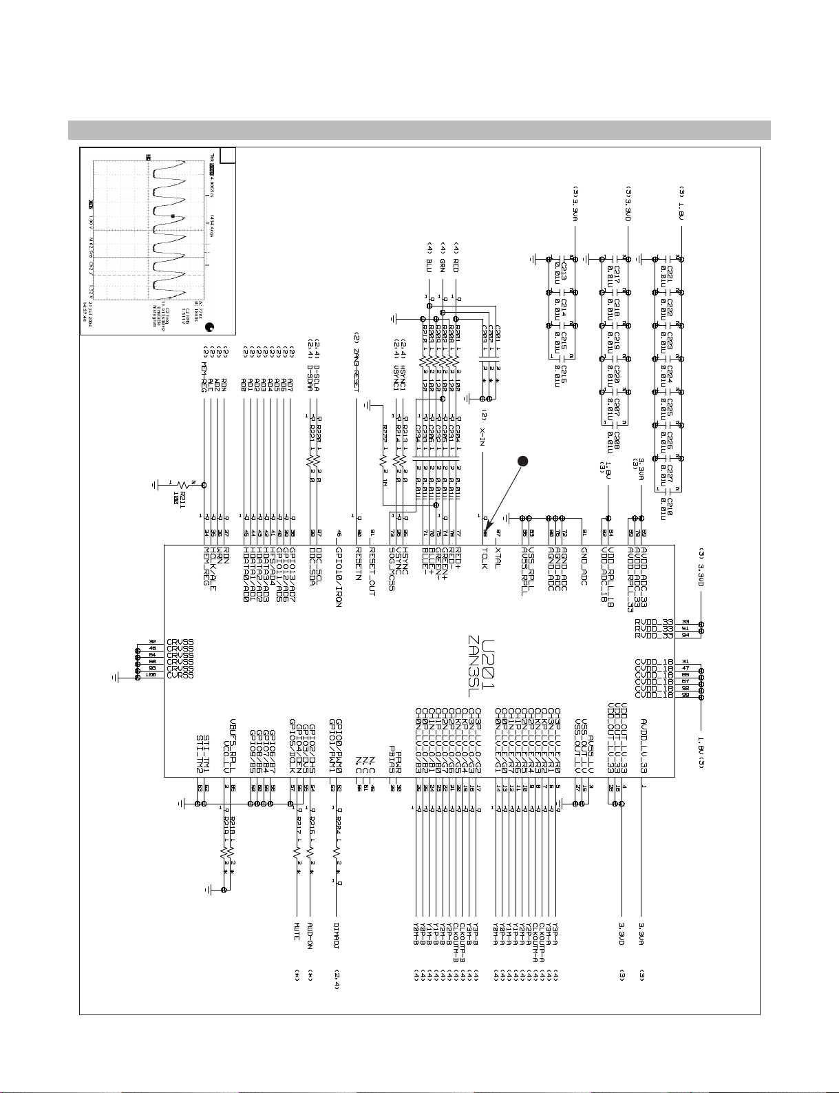
U201-#88
SCHEMATIC DIAGRAM
1. SCALER
# 1
L1750S/L1950S
ZAN3SL
2
- 23 -
Page 27
5
6
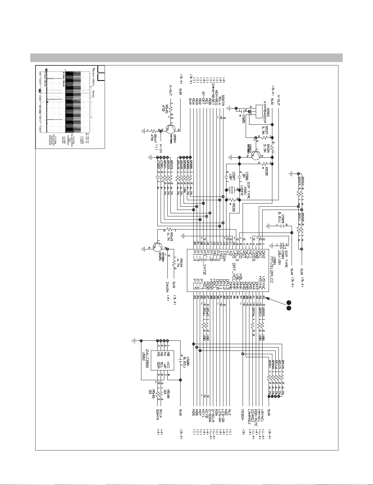
U501-#43, 44
2. MICOM
# 2
L1750S/L1950S
MICOM
- 24 -
5 6
1.5K(17")
Page 28
1
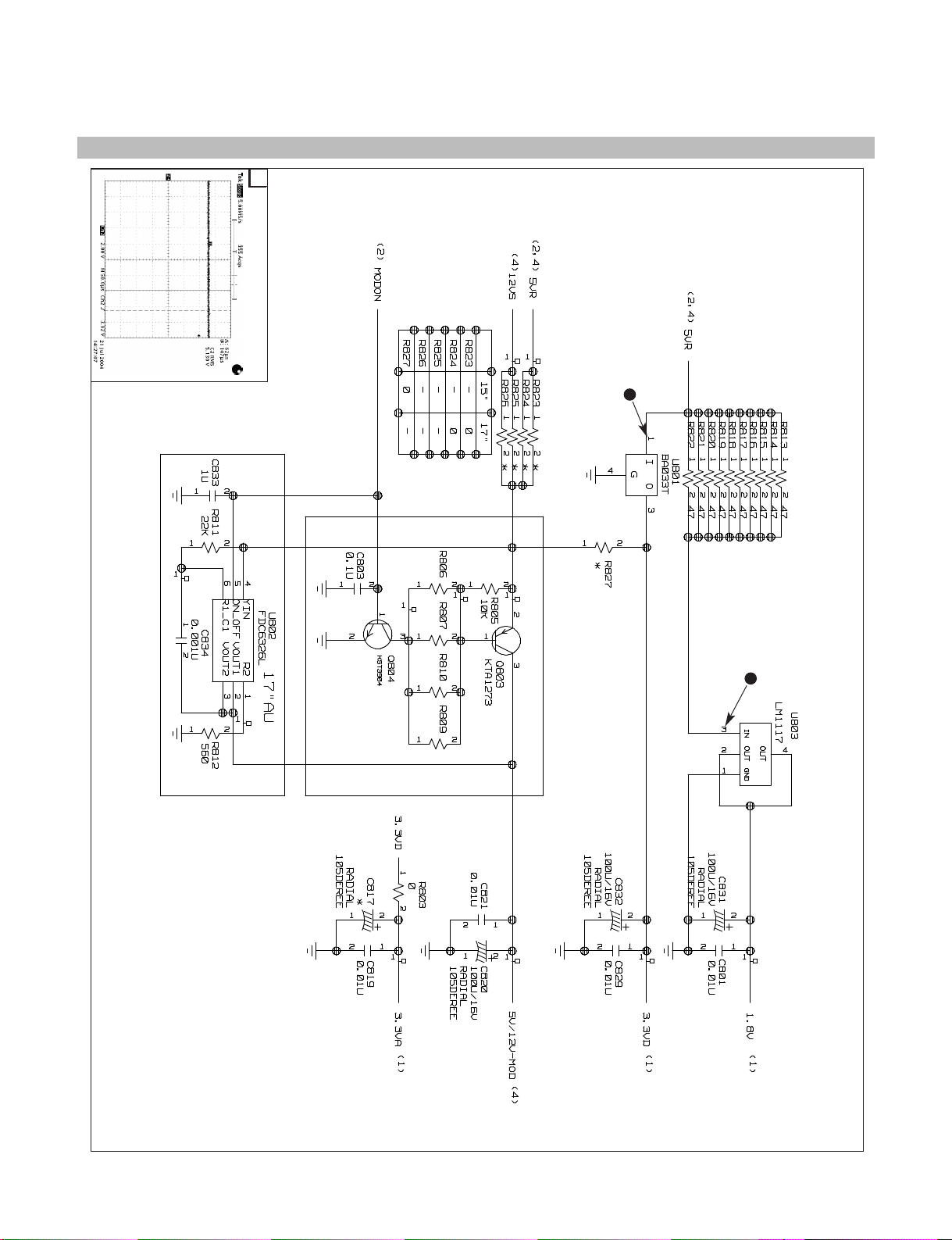
J707-#5,6/U801-#1/U803-#3
3. POWER
390
# 3
L1750S/L1950S
POWER
1
390
390 390
1
- 25 -
Page 29
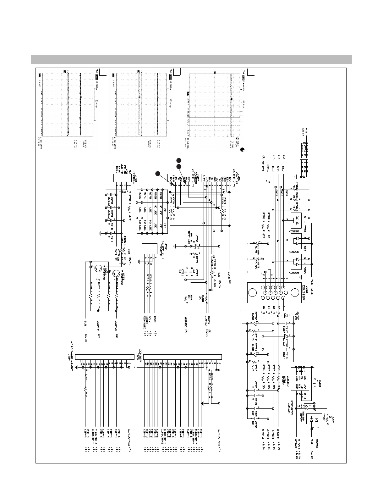
Inverter On
Micom Port check
J705 Inverter output
4
J707-#2
4. CONNECTOR & JACKS
3
J707-#2
Inverter Off
Micom Port check
J705 Inverter output
43
1
1
J707-#5,6/U801-#1/U803-#3
# 4
L1750S/L1950S
CONNECTOR & JACKS
15K
- 26 -
Page 30

Dec. 2004
P/NO : 3828TSL096P Printed in Korea
 Loading...