

Page 1

Embedded &
Industrial Computing
Hardware Platforms for Embedded and Industrial Computing
LEC-7100
>>
User's Manual
Publication date:2010-05-07
Page 2

About
About
Overview
Icon Descriptions
The icons are used in the manual to serve as an indication
of interest topics or important messages. Below is a
description of these icons:
NOTE: This check mark indicates that
there is a note of interest and is something
that you should pay special attention to
while using the product.
Online Resources
The listed websites are links to the on-line product
information and technical support.
Resource Website
Lanner http://www.lannerinc.com
Product Resources http://assist.lannerinc.com
WARNING: This exclamation point
indicates that there is a caution or
warning and it is something that could
damage your property or product.
Acknowledgement
Intel, Pentium and Celeron are registered trademarks of
Intel Corp.
Microsoft Windows and MS-DOS are registered trademarks
of Microsoft Corp.
All other product names or trademarks are properties of
their respective owners.
Compliances
CE
This product has passed the CE test for environmental
specifications. Test conditions for passing included the
equipment being operated within an industrial enclosure.
In order to protect the product from being damaged by
ESD (Electrostatic Discharge) and EMI leakage, we strongly
recommend the use of CE-compliant industrial enclosure
products.
FCC Class A
This equipment has been tested and found to comply
with the limits for a Class A digital device, pursuant to Part
15 of the FCC Rules. These limits are designed to provide
reasonable protection against harmful interference when
the equipment is operated in a commercial environment.
This equipment generates, uses and can radiate radio
frequency energy and, if not installed and used in
accordance with the instruction manual, may cause
harmful interference to radio communications. Operation
of this equipment in a residential area is likely to cause
harmful interference in which case the user will be required
to correct the interference at his own expense.
RMA http://eRMA.lannerinc.com
Copyright and Trademarks
This document is copyrighted, © 2010. All rights are
reserved. The original manufacturer reserves the right to
make improvements to the products described in this
manual at any time without notice.
No part of this manual may be reproduced, copied,
translated or transmitted in any form or by any means
without the prior written permission of the original
manufacturer. Information provided in this manual is
intended to be accurate and reliable. However, the original
manufacturer assumes no responsibility for its use, nor for
any infringements upon the rights of third parties that
may result from such use.
Embedded and Industrial Computing
i
Page 3

TTaTTable of Contentsbeable of Contents
Chapter 1: Introduction 1
System Specication . . . . . . . . . . . . . . . . . . . . . . . . . . . . . . . . . . . . . . . . . . . 1
Package Contents . . . . . . . . . . . . . . . . . . . . . . . . . . . . . . . . . . . . . . . . . . . . . 2
Front Panel Features. . . . . . . . . . . . . . . . . . . . . . . . . . . . . . . . . . . . . . . . . . . . 3
Rear Panel Features . . . . . . . . . . . . . . . . . . . . . . . . . . . . . . . . . . . . . . . . . . . . 4
Chapter 2: Hardware Setup 5
Preparing the Hardware Installation. . . . . . . . . . . . . . . . . . . . . . . . . . . . . . . . . . 5
Installing the System Memory . . . . . . . . . . . . . . . . . . . . . . . . . . . . . . . . . . . . . 5
Installing the Hard Disk . . . . . . . . . . . . . . . . . . . . . . . . . . . . . . . . . . . . . . . . . 5
Installing a CompactFlash Card. . . . . . . . . . . . . . . . . . . . . . . . . . . . . . . . . . . . . 6
3G SIM Card Installation . . . . . . . . . . . . . . . . . . . . . . . . . . . . . . . . . . . . . . . . . 6
Wireless 3G module Installation . . . . . . . . . . . . . . . . . . . . . . . . . . . . . . . . . . . . 6
Wall Mounting . . . . . . . . . . . . . . . . . . . . . . . . . . . . . . . . . . . . . . . . . . . . . . . 6
Chapter 3: Motherboard Information 7
Block Diagram . . . . . . . . . . . . . . . . . . . . . . . . . . . . . . . . . . . . . . . . . . . . . . . 7
Motherboard Layout . . . . . . . . . . . . . . . . . . . . . . . . . . . . . . . . . . . . . . . . . . . 8
Jumper Settings . . . . . . . . . . . . . . . . . . . . . . . . . . . . . . . . . . . . . . . . . . . . . . 9
Chapter 4: BIOS Settings 13
Accessing the BIOS menu . . . . . . . . . . . . . . . . . . . . . . . . . . . . . . . . . . . . . . . .13
Navigating the BIOS menu. . . . . . . . . . . . . . . . . . . . . . . . . . . . . . . . . . . . . . . .13
The Main Menu . . . . . . . . . . . . . . . . . . . . . . . . . . . . . . . . . . . . . . . . . . . . . . .14
Advanced Settings. . . . . . . . . . . . . . . . . . . . . . . . . . . . . . . . . . . . . . . . . . . . .14
Boot Settings . . . . . . . . . . . . . . . . . . . . . . . . . . . . . . . . . . . . . . . . . . . . . . . .25
Security Settings . . . . . . . . . . . . . . . . . . . . . . . . . . . . . . . . . . . . . . . . . . . . . .26
Exit Menu . . . . . . . . . . . . . . . . . . . . . . . . . . . . . . . . . . . . . . . . . . . . . . . . . .27
Appendix A: Programming Watchdog Timer 28
Appendix B: Setting up Remote Access 30
Appendix C: Digital Input/Output Control on the GPIO port 31
Appendix D: Terms and Conditions 34
Warranty Policy . . . . . . . . . . . . . . . . . . . . . . . . . . . . . . . . . . . . . . . . . . . .34
RMA Service . . . . . . . . . . . . . . . . . . . . . . . . . . . . . . . . . . . . . . . . . . . . . .34
ii
Page 4

Chapter 1
Introduction
Chapter 1: Introduction
Thank you for choosing the LEC-7100. The LEC-7100 is
Lanner’s flagship IPC. It features the Dual Core Intel®
Atom™ D510 processor that has 1.66GHz of processing
power. Utilizing the Atom’s ability for performance with
very low heat generation allows the LEC-7100 to be a
completely fanless system.
The LEC-7100 is an ideal solution for application ready
system platform. All electronics are protected in a compact
sealed aluminum case as a stand-alone unit and can be
easily situated in a place where space is limited and the
environment is harsh.
A solid sealed Aluminum extrusion framing provides
vibration and dust resistance while providing a passive
cooling solution. It also provides great protection from
EMI, shock, and vibration.
The LEC-7100 answers the demand for versatile I/O
interfaces by offering 1 x DVI-I interface and 1x VGA
interface for dual display, 6x USB 2.0 ports (2 internal), 2 x
Giga LAN port, audio function, 2x COM ports (1 internal),
and 2 PCI-e slots; all of theses are equipped onto a small
rugged unit. The LEC-7100 also supports 1 x 2.5 SATA HDD
and 1 x Compact Flash card for storage options.
Please refer to the following chart below for a summary of
the system’s specifications.
System Specification
FEATURE DESCRIPTION
Form Factor Embedded Fanless System
Processor Onboard Intel D510
Platform
Memory
Storage
Controller
Video
Audio
I/O
Hardware Monitor
OS Supported
Environmental
Parameters
Dimensions
Power
Compliance
Chipset Intel ICH8M
BIOS AMIBIOS with 8Mbit FWH
Max. FSB 667MHz
Memory Socket SODIMM x 1 (up to 2GB)
Max Memory 2GB (Module)
Compact Flash CF Socket Type I/II x1
HDD 2.5” SATA HDD support
Controller (Interface) RTL8111C(D) (PCIe 1X)
Controller Intel Gen 3.5 GFX Core
Codec ALC888 HD Codec
COM Ports RS-232 x 1
Digital I/O DB9 Female, 4 in 4 Out
USB 2.0 4 (External x 4)
Onboard SIM card Socket
VGA 1 (2048 x 1536 / 75Hz)
DVI-D 1 (1280 x 800)
LAN RJ45 GbE x 2
Audio Stereo Line Out (RCA L/R)
Internal CF 1
DC-in Connector Type Power Jack w/Lock
Expansion Mini-PCIe x 2, Mini-PCI x 1
Controller
Watchdog timer Yes (1~255 level)
Operating Temperature
(With Industrial Components:
CF, Memory, SSD, HDD)
Operating Temperature
(With Commercial Components)
W x H x D (mm) 268(W) x 44(H) x 174(D)
W x H x D (Inch) 10.55”(W) x 1.73”(H) x 6.85”(D)
Input (Mode) DC +12V (ATX Mode)
AC Adapter
1 to be used with mini-PCIe 3G/
GPS module
Winbond W83627 UHG integrated
hardware monitor
Linux kernel 2.4.16 or above, XPE/
Win XP-32 bit, Windows 7
-10°~55°C / 14°~131°F
-5°C~45°C / 23°~113°F
AC Adapter D: 60W (+12V)
Power Jack w/Lock
CE, FCC, RoHS
Embedded and Industrial Computing
1
Page 5

Chapter 1
Package Contents
Your package contains the following items:
LEC-7100 Embedded System •
DC+12V 60W Power Adapter •
Serial-ATA/Power Cable •
Wall-Mounting Kit •
Drivers and User’s Manual CD •
Introduction
Embedded and Industrial Computing
2
Page 6

Chapter 1
Front Panel Features
Introduction
F1
F1 VGA Port: DB-15 Female Connector
Using suitable DB-15 cable, you can connect an appropriate device such as a monitor.
F2 DVI-D Port: DVI-D Dual Link Connector
By using suitable DVI-D dual link cable, you can connect an appropriate device such as an
LCD panel. It allows a maximum resolution of 1280x800 pixels.
F3 Audio-right
RCA Jack for right audio out
F4 Audio-left
RCA Jack for left audio out
F5 Two 10/100/1000Mbps LAN ports: LAN1-left, LAN2-right
Using suitable RJ-45 cable, you can connect LEC-7100 System to a computer, or to any
other piece of equipment that has an Ethernet connection, for example, a hub or a
switch. Moreover, both of them have Wake-on-LAN and Preboot Execution Environment
capabilities.
F2
F3
F4
F5 F7
F6
F6 Power Adapter socket with Lock
DC-in 12V jack. Only use the power adapter supplied with the LEC-7100 System.
F7 LED Indicators: Yellow-HDD LED, Green-Power LED
HDD LED: A hard disk LED. If the LED is on, it indicates that the system’s storage is
functional. If it is off, it indicates that the system’s storage is not functional. If it is flashing,
it indicates data access activities.
Power Led: Green indicates that the system is powered on.
Embedded and Industrial Computing
3
Page 7

Chapter 1
Rear Panel Features
Introduction
R1
R1 Reset Switch
It is a hardware reset switch. Use this switch to reset the system without
turning off the power.
R2 DIO Port (DB-9 female connector)
The general-purpose input/output (GPIO) peripheral provides dedicated
general-purpose pins to support connection of digital I/O devices.
R3 RS-232 COM Port (DB-9 Male Connector)
Using suitable RS-232 cable, you can connect an appropriate device, for
example, a terminal console for diagnostics. This port is assigned as COM1.
The default configuration parameter: 9600 baud rate, 8 data bits, no parity,
1stop bit, and no flow control.
R4 Four USB 2.0 Ports
It connects to any USB devices such as a flash drive. The left-bottom one is
defined as USB0 whereas the left-upper one is USB1; the right-bottom one
is defined as USB2 whereas the right-upper one is USB3.
R2
R3
F4
R5
R6
R5 Power Switch through Phoenix Contact
It is a power-on switch. You could turn on or off the system power by using
this contact in stead of the following power switch.
R6 Power-on Switch
If the LED is green, it indicates that the system is powered on; if the LED is
red, it indicates that the system is in Standby mode.
Embedded and Industrial Computing
4
Page 8

Chapter 2
Introduction
Chapter 2: Hardware Setup
Preparing the Hardware Installation
To access some components and perform certain service
procedures, you must perform the following procedures
first.
WARNING: To reduce the risk of personal injury,
electric shock, or damage to the equipment,
remove the power cord to remove power from the
server. The front panel Power On/Standby button
does not completely shut off system power.
Portions of the power supply and some internal
circuitry remain active until AC power is removed.
Unpower the LEC-7100 and remove the power cord.1.
Unscrew the 3 threaded screws from the top cover of 2.
the LEC-7100 System.
Slide the cover backwards and open the cover 3.
Note:
All SO-DIMMs installed must be the same speed 1.
(DDR2 667). Do not install DIMMs supporting
different speeds.
The motherboards can support up to 2 GB 2.
memory capacity in maximum.
Installing the Hard Disk
The system can accomdate two Serial-ATA disks. Follow
these steps to install a hard disk into the LEC-7100:
Unsrew the 4 screws on the hard disk tray to take out 1.
the hard disk tray from the system.
Place hard disk on the hard disk tray and align the holes 2.
of the hard disk with the mounting holes on the tray.
Secure the hard disk with 4 mounting screws on the 3.
hard disk tray.
Connect the Serial-ATA power and hard disk cables to 4.
the hard disk’s connectors respectively.
Plug the Serial-ATA cable to the Serial-ATA Connector 5.
on the main board.
upwards.
Installing the System Memory
The motherboard supports DDR2 memory that features
data transfer rates of 667 MHz to meet the higher
bandwidth requirements of the latest operating system
and Internet applications. It comes with two Double Data
Rate(DDR2) Small Outline Dual Inline Memory Modules
(SO-DIMM) sockets.
Open the DIMM slot latches.1.
Install the DIMM.2.
Notch
Cutout
Put the hard disk tray with the installed hard disk back 6.
to the system and secure it with the mounting screws.
Put the hard disk tray with the installed hard disk back 7.
to the system and secure it with the mounting screws.
1
2
Embedded and Industrial Computing
5
Page 9

Chapter 2
Introduction
Installing a CompactFlash Card
LEC-7100 provides one CompactFlash slot(CF1). Follow
the procedures bellow for installing a CompactFlash card.
Align CompactFlash card and the card slot with the 1.
arrow pointing toward the connector.
Push the card to insert into the connector.2.
1
2
3G SIM Card Installation
Open the SIM tray and flip it diagnolly.1.
Align the cut-off angle of the SIM card with the SIM 2.
card socket. Also place the ICs facing up.
Note:
To remove the module from the system, release 1.
the latch first by slightly bending it inward.
To remove the SIM card, unlock the tray first by 2.
sliding it outward.
Wall Mounting
The product ships with wall mounting kit. To mount your
product on the wall, follow the instructions below:
First make a hole for the anchor in the surface on the 1.
wall.
Then press the anchor into the hole until it is flush with 2.
the surface. You may need a hammer to tap the wall
anchor.
Use a screwdriver to screw the threaded screw into the 3.
plastic anchor.
Attach the wall mounting bracket to the back of the 4.
device, securing it in place with four of the flat-head
screws provided.
Hang the device on the wall.5.
Insert the 3. SIM card into the tray diagnoally. Close and
lock the tray.
Wireless 3G module Installation
Align the wireless module’s cutout with the Mini-PCIe 1.
slot notch.
Insert the wireless module into the connector 2.
diagnoally.
Push the other end of the wireless module to be 3.
tightened with the latch.
3G module
2
SIM Card
2
3
Embedded and Industrial Computing
6
Page 10

Chapter 3
Chapter 3: Motherboard Information
Block Diagram
The block diagram depicts the relationships among the
interfaces or modules on the motherboard. Please refer
to the following figure for your motherboard’s layout
design.
Motherboard Information
Embedded and Industrial Computing
7
Page 11
Chapter 3
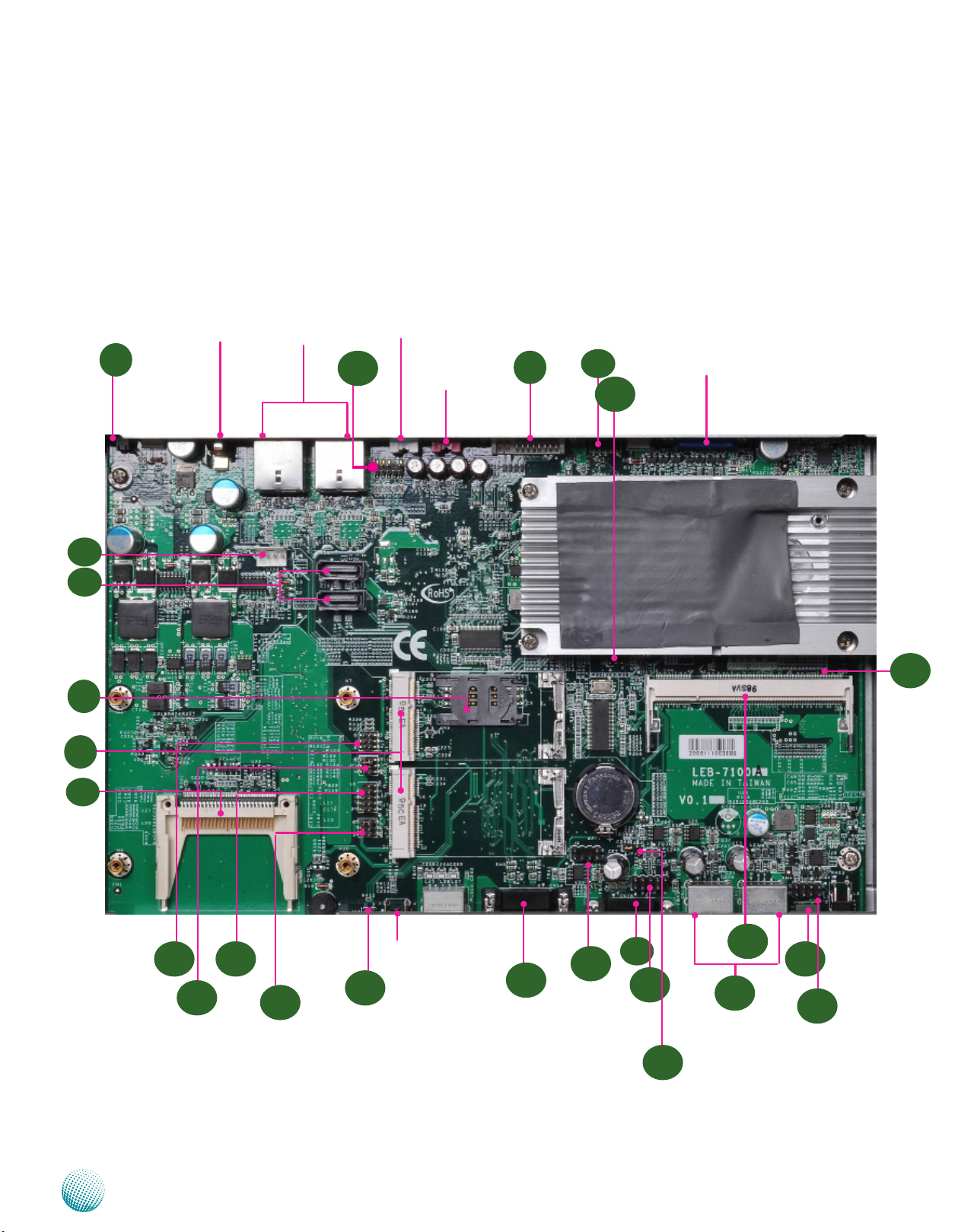
Motherboard Layout
The motherboard layout shows the connectors and
jumpers on the board. Refer to the following picture
as a reference of the pin assignments and the internal
connectors.
Motherboard Information
M5
M4
M6
M8
M1
DC-in 12V
Jack(CN7
LAN1(CN6)/
)
LAN2(CN5)
Lineout-L(CN1):
M22
Lineout-R(CN2)
M2
M3
E x t e rn al V G A
Connector(CN4)
M23
M25
Mini-PCI
Connector(at
the back)
M7
M13
Embedded and Industrial Computing
M15
M12
M14
HW Reset(SW1)
M24
M18
M19
M9
M20
M10
M17
M16
M21
M11
8
Page 12

Chapter 3
Motherboard Information
Jumper Settings
M1
Power/Hard Disk LED (LED1): The power and hard disk
LED indicator.
Pin No. Function Pin No. Function
C2 HDD LED N A2 HDD LED P
C1 PWD LED N A1 PWR LED P
M2
DVI-D Connector(CN3): The DVI (Digital Visual
Interface) is a standard for high resolution digital
displays. Below is a 24-Pin DVI Female connector ‘s
pinout.
Pin No. Function Pin No. Function
1 TMDS Data2- 13 Reserved
2 TMDS Data2+ 14 +5V Power
3 Ground 15 Ground (for+5V)
4 Reserved 16 Hot Plug Detect
5 Reserved 17 TMDS Data()-
6 Reserved 18 TMDS Data()+
7 Reserved 19 Ground
8 Reserved 20 Reserved
9 TMDS Data1- 21 Reserved
10 TMDS Data 1+ 22 TMDS Clock Shield
11 Ground 23 TMDS Clock +
12 Reserved 24 TMDS Clock -
Note that some pins are assigned as Reserved which is different from the
M3
SPI-ROM(J1): Using the appropriate cable to connect
this 10-pin ISP in header connector, the user can
update the SPI Flash soldered on board
Pin No. Function
1 SPI_HOLD_N
3 SPI_CS0_N
5 SPI_MISO
7 RSVD
9 GND
M4
Serial-ATA Connector (J4/J5): It is for connecting a 2.5''
SATA harddisk to be served as your system's storage.
M5
4-pin Serial-ATA Power Connector (J3): It is for
connectig the SATA power cord.
4 3 2 1
M6
SIM Socket (CN9): It is for connecting SIM card of the
mobile connection.
M7
Compact Flash Connector (CN11): It is for connecting
a Compact Flash card to be served as your system's
storage.
standard DVI-D pinout.
2 4 6 8 10
1 3 5 7 9
Pin No. Function
Pin No. Function
2 RSVD
4 +3.3V
6 RSVD
8 SPI_CLK
10 SPI_MOSI
1 5V
2 Ground
3 Ground
4 12V
M8
Mini-PCIe Socket(CN10/CN12): It is for connecting
any Mini-PCIe adapter such as a Wi-Fi module (CN10)
or connecting Wireless 3G module (CN12) for mobile
Internet connections.
CN10 Pin Assignment
PIN NO. Description PIN NO. Description
1 WAKE# 2 3.3V
3 Reserved 4 GND
5 Reserved 6 1.5V
7 CLKREQ# 8 UIM_PWR
9 GND 10 UIM_DATA
11 REFCLK- 12 UIM_CLK
13 REFCLK+ 14 UIM_RESET
15 GND 16 UIM_VPP
17 Reserved (UIM_C8) 18 GND
19 Reserved (UIM_C4) 20 ENABLE
21 GND 22 PERST#
23 PERn0 24 +3.3Vaux
25 PERp0 26 GND
27 GND 28 +1.5V
29 GND 30 SMB_CLK
31 PETn0 32 SMB_DATA
33 PETp0 34 GND
35 GND 36 USB_D37 Reserved 38 USB_D+
39 Reserved 40 GND
41 Reserved 42 LED_
WWAN#
43 Reserved 44 LED_
WLAN#
45 Reserved 46 LED_
WPAN#
47 Reserved 48 +1.5V
49 Reserved 50 GND
51 Reserved 52 +3.3V
CN12 Pin Assignment
PIN NO. Description PIN NO. Description
1 WAKE# 2 3.3V
3 Reserved 4 GND
5 Reserved 6 1.5V
7 CLKREQ# 8 Reserved
9 GND 10 Reserved
11 REFCLK- 12 Reserved
13 REFCLK+ 14 Reserved
15 GND 16 Reserved
17 Reserved (UIM_C8) 18 GND
19 Reserved (UIM_C4) 20 ENABLE
21 GND 22 PERST#
23 PERn0 24 +3.3Vaux
25 PERp0 26 GND
27 GND 28 +1.5V
29 GND 30 SMB_CLK
31 PETn0 32 SMB_DATA
33 PETp0 34 GND
35 GND 36 USB_D37 Reserved 38 USB_D+
Embedded and Industrial Computing
9
Page 13

Chapter 3
Motherboard Information
39 Reserved 40 GND
41 Reserved 42 Reserved
43 Reserved 44 Reserved
45 Reserved 46 Reserved
47 Reserved 48 +1.5V
49 Reserved 50 GND
51 Reserved 52 +3.3V
M9
RS-232 COM Port(COM1, CN18): It is the RS-232 serial
port.
Pin
No.
1 Data Carrier Detectg
2 Receive Data
3 Transmit Data
4 Data Terminal Ready
5 Ground
M10
Pin Name
12345
6789
SO-DIMM Socket (CN8): It is for connecting the DDR2
Pin
No.
6 Data Set Ready
7 Request to Send
8 Clear to Send
9 Ring Indicator
667 (200 pin) memory. The system can suport up to 2
GB in maximum.
M11
Clear CMOS jumper (JP3): It is for clearing the CMOS
memory.
Pin No. Function
1-2 Normal (Default)
2-3 Clear CMOS
M12 M14
1 2 3
Ring-indicator Jumper Setting (JP1, JP2): The
Ring indicator pinout of the RS-232 COM port (JP2 for
COM1 and JP1 for COM2) can be altered according to
the following jumper settings.
5
6
3
4
1
2
Pin No. Function
1-2 Supply +5V to Device
3-4 Supply +12V to Device
5-6 RS-232 Ring
Pin Name
M13
Mini-PCIe Wireless LED(J7): It shows the wireless
connection status for wireless modules connected in
Mini-PCIe Socket.
Function Pin No.
LED1R_WPLAN_N 6
LED1R_WLAN_N 4
LED1R_WWAN_N 2
M15
RS-232 COM Port(COM2, J8): It is for connecting the
6
4
2
Pin No. Function
5
5 LED1_WPAN_N
3
3 LED1_WLAN_N
1
1 LED1_WWAN_N
RS-232 interface cable .
Pin No. Function
Key 10
Ring Indicator 8
Clear to Send 6
Request to Send 4
Data Set Ready 2
M16
USB Ports (No. 0/1/2/3): The system provides 4
10
8
6
4
2
Pin No. Function
9
9
7
7
5
3
1
Data Terminal Ready
5
3
1
Data Carrier Detected
Signal Ground
Transmitted Data
Received Data
external USB [CN16 for USB0, USB1 (the bottom one
is USB0; the upper one is USB1) and CN17 for USB2,
USB3 (the bottom one is USB2; the upper one is
USB3)] type A connectors.
Embedded and Industrial Computing
10
Page 14

Chapter 3
Motherboard Information
Pin No. Function
5 USB_VCC
6 USBD17 USBD1+
8 GND
5 6 7 8
1 2 3 4
Pin No. Function
1 USB_VCC
2 USBD03 USBD0+
4 GND
M17
Power Switch through Phoenix Contact(J12)
1 2
M18
DIO Ports(CN14): The 8 pins of General Purpose Input/
Pin No. Function
1
2
Pin No. Function
5 USB_VCC
6 USBD37 USBD3+
8 GND
5 6 7 8
1 2 3 4
Pin No. Function
1 USB_VCC
2 USBD23 USBD2+
4 GND
1 PWR_BTN_N
GND
Output (GPIO) can be can be configured as an either
input or output through the DB-9 female connector.
Pin No. Pin Name
1 Input0
2 Input1
3 Input2
4 Input3
5 GND
5 4321
9 8 7 6
Pin No. Pin Name
6 Output0
7 Output1
8 Output2
9 Output3
M21
Miscellaneous Pin Header (J11): Theses pin headers
can be used as a backup for the following functions:
Harddisk LED, Reset Button, and Power LED indicator.
PIN No. Function
1 HardDisk LED
3 HardDisk_LED_N
5 FP_RST_BTN_N
7 GND
7531
8 6 4 2
PIN No. Function
2 PWDLED
4 PWROK_100MS_N
6 FP_PWR_BTN_N
8 GND
M22
Internal Audio Connector(J2): It is an redundant pin
header for connecting an audio interface cable.
PIN NO. LINE_OUT2_L GND MIC_OUT_L GND
Function 2 4 6 8 10
246810
13579
Pin No. 1 3 5 7 9
Pin Name LINE_OUT2_R GND MIC_OUT_R LINE_IN_R LINE_IN_L
M19
PS/2 Keyboard & Mouse Connector (J9): It is for
connecting the PS/2 keyboard and mouse interface
cable.
Pin No. Pin Name
1 VCC
3 MSDATA
5 KBDATA
7 GND
M20
Dual USB Interface Connector (J10 for USB No.4 and
2 4 6 8
1 3 5 7
Pin No. Pin Name
2 MSCLK
4 KEY
6 KEY
8 KBCLK
No.5): It is for connecting the USB module cable. It
complies with USB2.0 and support up to 480 Mbps
connection speed.
Function USB_VCC USBD5- USBD5+ GND NC
PIN NO. 2 4 6 8 10
PIN NO. 1 3 5 7 9
Function USB_VCC USBD4- USBD4+ GND
2 4 6 8 10
1 3 5 7 9
M23
SM-Bus Reserved (J6): System Management Bus.
It can be connected to read the value of the CPU
register.
Pin No. Pin Name
1 2 3
M24
Thermal Sensor Connector(J13): It is for connecting
1 Smbdata
2 GND
3 SmbCLK
a temperature monitor.
Pin No. Pin Name
1 2
Mini-PCI Connector (at the back, CN19)
M25
1 System_temp
2 GND
Embedded and Industrial Computing
11
Page 15

Chapter 3
Motherboard Information
PIN NO. Description Pin No. Description
1 TIP 2 RING
3 8PMJ-3 4 8PMJ-1
5 8PMJ-6 6 8PMJ-2
7 8PMJ-7 8 8PMJ-4
9 8PMJ-8 10 8PMJ-5
11 LED1_GRNP 12 LED2_YELP
13 LED1_GRNN 14 LED2_YELP
15 CHSGND 16 RESERVED
17 INT-B 18 +5V
19 +3.3V 20 INT-A
21 RESERVED 22 RESERVED
23 GROUND 24 3.3VAUX
25 CLK 26 RST
27 GROUND 28 +3.3V
29 REO 30 GNT
31 +3.3V 32 GROUND
33 AD31 34 PME
35 AD29 36 RESERVED
37 GROUND 38 AD30
39 AD27 40 +3.3V
41 AD25 42 AD28
43 RESERVED 44 AD26
45 C_BE-3 46 AD24
47 AD23 48 IDSEL
49 GROUND 50 GROUND
51 AD21 52 AD22
53 AD19 54 AD20
55 GROUND 56 PAR
57 AD17 58 AD18
59 C_BE-2 60 AD16
61 IRDY 62 GROUND
63 +3.3V 64 FRAME
65 CLKRUN 66 TRDY
67 SERR 68 STOP
69 GROUND 70 +3.3V
73 C_BE-1 74 GROUND
75 AD14 76 AD15
77 GROUND 78 AD13
79 AD12 80 AD11
81 AD10 82 GROUND
83 GROUND 84 AD9
85 AD8 86 C_BE-0
87 AD7 88 +3.3V
89 +3.3V 90 AD6
91 AD5 92 AD4
93 RESERVED 94 AD2
95 AD3 96 AD0
97 +5V 98 RESERVED-WIP
99 AD1 100 RESERVED-WIP
101 GROUND 102 GROUND
103 AC_SYNC 104 M66EN
105 AC_SDATA_IN 106 AC_SDATA_
OUT
107 AC_BIT_CLK 108 AC_CODEC_ID0
109 AC_CODEC_ID1 110 AC_RESET
111 MOD_AUDIO_
MON
113 AUDIO_GND 114 GROUND
112 RESERVED
PIN NO. Description Pin No. Description
115 SYS_AUDIO_
OUT
117 SYS_AUDIO_
OUT GND
119 AUDIO_GND 120 AUDIO_GND
121 RESERVED 122 MPCIACT
123 VCC5VA 124 3.3AUX
116 SYS_AUDIO_IN
118 SYS_AUDIO_IN
GND
Embedded and Industrial Computing
12
Page 16

Chapter 4
Bios Settings
Chapter 4: BIOS Settings
Accessing the BIOS menu
Use the BIOS Setup program when you are installing a
motherboard, reconfiguring your system, or prompted to
“Run Setup.” This section explains how to configure your
system using this utility.
Even if you are not prompted to use the Setup program,
you can change the configuration of your computer in the
future. For example, you can enable the security password
feature or change the power management settings. This
requires you to reconfigure your system using the BIOS
Setup program so that the computer can recognize these
changes and record them in the CMOS RAM .
When you start up the computer, the system provides you
with the opportunity to run this program. Press <Delete>
during the Power-On Self-Test (POST) to enter the Setup
utility(There are a few cases that other keys are used, such
as <F1>, <F2>, and so on.); otherwise, POST continues
with its test routines.
If you wish to enter Setup after POST, restart the system
by pressing <Ctrl+Alt+Delete>, or by pressing the reset
button on the system chassis. You can also restart by
turning the system off and then back on. Do this last
option only if the first two failed.
The Setup program is designed to make it as easy to use as
possible. Being a menu-driven program, it lets you scroll
through the various sub-menus and make your selections
from the available options using the navigation keys.
Note: This manual describes the standard look
of the setup screen. The motherboard manufacturer
has the ability to change any and all of the settings
described in this manual. This means that some of the
options described in this manual do not exist in your
motherboard’s AMIBIOS.
Navigating the BIOS menu
The BIOS setup/utility uses a key-based navigation system
called hot keys. Most of the BIOS setup utility hot keys can
be used at any time during the setup navigation process.
These keys include <F1>, <F10>, <Enter>, <ESC>, <Arrow>
keys, and so on.
Keys Description
-><- Left/Right The Left and Right <Arrow>
keys allow you to select an
setup screen.
For example: Main screen,
Advanced screen, Chipset
->
Up/Down The Up and Down <Arrow>
->
+- Plus/Minuss The Plus and Minus <Arrow>
Tab The <Tab> key allows you to
screen, and so on.
keys allow you to select an
setup item or sub-screen.
keys allow you to change the
field value of a particular setup
item.
For example: Date and Time.
select setup fields.
Embedded and Industrial Computing
13
Page 17

Chapter 4
The Main Menu
The main BIOS setup menu is the first screen that you can
navigate. Each main BIOS setup menu option is described
in this chapter.
The Main BIOS setup menu screen has two main frames.
The left frame displays all the options that can be
configured. “Grayed-out” options cannot be configured.
Options is blue can be.
The right frame displays the key legend. Above the key
legend is an area reserved for a text message. When an
option is selected in the left frame, it is highlighted in
white. Often a text message will accompany it.
System Time/System Date
Use this option to change the system time and date.
Highlight System Time or System Date using the <Arrow>
keys. Enter new values through the keyboard. Press the
<Tab> key or the <Arrow> keys to move between fields.
The date must be entered in MM/DD/YY format. The time
is entered in HH:MM:SS format.
Bios Settings
Advanced Settings
Select the Advanced tab from the setup screen to enter
the Advanced BIOS Setup screen. You can select any of
the items in the left frame of the screen, such as SuperIO
Configuration, to go to the sub menu for that item. You
can display an Advanced BIOS
Setup option by highlighting it using the <Arrow> keys.
All Advanced BIOS Setup options are described in this
section. The Advanced BIOS Setup screen is shown at
the right. The sub menus are described on the following
pages.
IDE Configuration Settings
You can use this screen to select options for the IDE
Configuration Settings. Use the up and down <Arrow>
keys to select an item. Use the <Plus> and <Minus> keys to
change the value of the selected option. A description of
the selected item appears on the right side of the screen.
The settings are described on the following pages. An
example of the IDE Configuration screen is at the right.
Primary IDE Master, Primary IDE Slave, Secondary IDE Master,
Secondary IDE Slave:
Select one of the hard disk drives to configure it. Press
<Enter> to access its the sub menu. The options on the
sub menu are described as in the following..
Hard disk drive Write Protect
Set this option to protect the hard disk drive from being
overwritten. The Load Optimal default setting is Disabled.
Embedded and Industrial Computing
14
Page 18

Chapter 4
Option Description
Disabled Set this value to allow the hard disk drive
to be used normally. Read, write, and erase
functions can be performed to the hard disk
drive. This is the default setting.
Enabled Set this value to prevent the hard disk drive
from being erased.
IDE Detect Time Out (Seconds)
Set this option to stop the AMIBIOS from searching for IDE
devices within the specified number of seconds. Basically,
this allows you to fine-tune the settings to allow for faster
boot times. Adjust this setting until a suitable timing that
can detect all IDE disk drives attached is found.
The Load Optimal default setting is 35.
Option Description
0 This value is the best setting to use if the onboard
IDE controllers are set to a specific IDE disk drive in
the AMIBIOS.
5 Set this value to stop the AMIBIOS from searching
the IDE bus for IDE disk drives in five seconds. A
large majority of ultra ATA hard disk drives can be
detected well within five seconds.
10 Set this value to stop the AMIBIOS from searching
the IDE bus for IDE disk drives in 10 seconds.
15 Set this value to stop the AMIBIOS from searching
the IDE bus for IDE disk drives in 15 seconds.
20 Set this value to stop the AMIBIOS from searching
the IDE bus for IDE disk drives in 20 seconds.
25 Set this value to stop the AMIBIOS from searching
the IDE bus for IDE disk drives in 25 seconds.
30 Set this value to stop the AMIBIOS from searching
the IDE bus for IDE disk drives in30 seconds.
35 Set this value to stop the AMIBIOS from searching
the IDE bus for IDE disk drives in 35 seconds.
Bios Settings
Embedded and Industrial Computing
15
Page 19

Chapter 4
Primary and Secondary IDE Master and Slave Settings
From the IDE Configuration screen, press <Enter> to
access the sub menu for the primary and secondary IDE
master and slave drives. Use this screen to select options
for the Primary and Secondary IDE drives. Use the up and
down <Arrow> keys to select an item. Use the <Plus> and
<Minus> keys to change the value of the selected option.
The settings are described on the following pages. The
screen for the Primary IDE Master is shown at the right.
Type
This option sets the type of device that the AMIBIOS
attempts to boot from after the Power-On Self-Test (POST )
has completed. The Load Optimal default setting is Auto.
Option Description
Not Installed Set this value to prevent the BIOS from
searching for an IDE disk drive on the specified
channel.
Auto Set this value to allow the BIOS auto detect the
IDE disk drive type attached to the specified
channel. This setting should be used if an IDE
hard disk drive is attached to the specified
channel. This is the default setting.
CDROM This option specifies that an IDE CD-ROM drive
is attached to the specified IDE channel. The
BIOS will not attempt to search for other types
of IDE disk drives on the specified channe.
ARMD This option specifies an ATAPI Removable
Media Device.
Bios Settings
This includes, but is not limited to:
• ZIP
• LS-120
LBA/Large Mode
LBA (Logical Block Addressing) is a method of addressing
data on a disk drive. In LBA mode, the maximum drive
capacity is 137 GB. The Load Optimal default setting is
Auto.
Option Description
Disabled Set this value to prevent the BIOS from using
Large Block Addressing mode control on the
specified channel.
Auto Set this value to allow the BIOS to auto detect
the Large Block Addressing mode control on the
specified channel. This is the default setting.
Embedded and Industrial Computing
16
Page 20

Chapter 4
Note: For drive capacities over 137 GB,
your AMIBIOS must be equipped with 48-bit LBA
mode ddressing. If not, contact your motherboard
manufacturer or install an ATA/133 IDE controller card
that supports 48-bit LBA mode.
Block (Multi-Sector Transfer)
This option sets the block mode multi sector transfers
option. The Load Optimal default setting is Auto.
Option Description
Disabled Set this value to prevent the BIOS from using
Multi-Sector Transfer on the specified channel.
The data to and from the device will occur one
sector at a time.
Auto Set this value to allow the BIOS to auto detect
device support for Multi-Sector Transfers on the
specified channel. If supported, Set this value
to allow the BIOS to auto detect the number of
sectors per block for transfer from the hard disk
drive to the memory. The data transfer to and
from the device will occur multiple sectors at a
time. This is the default setting.
Bios Settings
PIO Mode
IDE PIO (Programmable I/O) mode programs timing
cycles between the IDE drive and the programmable
IDE controller. As the PIO mode increases, the cycle time
decreases. The Load Optimal default setting is Auto.
Option Description
Auto Set this value to allow the BIOS to auto detect
the PIO mode. Use this value if the IDE disk
drive support cannot be determined. This is the
default setting.
0 Set this value to allow the BIOS to use PIO mode
0. It has a data transfer rate of 3.3 MBs.
1 Set this value to allow the BIOS to use PIO mode
0. It has a data transfer rate of 5.2 MBs.
2 Set this value to allow the BIOS to use PIO mode
0. It has a data transfer rate of 8.3 MBs.
3 Set this value to allow the BIOS to use PIO mode
0. It has a data transfer rate of 11.1MBs.
4 Set this value to allow the BIOS to use PIO
mode 4. It has a data transfer rate of 16.6 MBs.
This setting generally works with all hard disk
drives manufactured after 1999. For other disk
drive, such as IDE CD-ROM drives, check the
specifications of the drive.
DMA Mode
This setting allows you to adjust the DMA mode options.
The Load Optimal default setting is Auto.
Embedded and Industrial Computing
17
Page 21

Chapter 4
Option Description
Auto Set this value to allow the BIOS to auto detect
the DMA mode. Use this value if the IDE disk
drive support cannot be determined. This is the
default setting.
SWDMA0 Set this value to allow the BIOS to use Single
Word DMA mode 0. It has a data transfer rate of
2.1 MBs.
SWDMA1 Set this value to allow the BIOS to use Single
Word DMA mode 1. It has a data transfer rate of
4.2 MBs.
SWDMA2 Set this value to allow the BIOS to use Single
Word DMA mode 1. It has a data transfer rate of
8.3 MBs.
MWDMA0 Set this value to allow the BIOS to use Multi Word
DMA mode 0. It has a data transfer rate of 4.2
MBs.
MWDMA1 Set this value to allow the BIOS to use Multi Word
DMA mode 0. It has a data transfer rate of 13.3
MBs.
MWDMA2 Set this value to allow the BIOS to use Multi Word
DMA mode 0. It has a data transfer rate of 16.6
MBs.
UDMA0 Set this value to allow the BIOS to use Ultra DMA
mode 0. It has a data transfer rate of 16.6 MBs.
It has the same transfer rate as PIO mode 4 and
Multi Word DMA mode 2.
UDMA1 Set this value to allow the BIOS to use Ultra DMA
mode 1. It has a data transfer rate of 25 MBs.
UDMA2 Set this value to allow the BIOS to use Ultra DMA
mode 1. It has a data transfer rate of 33.3 MBs.
UDMA3 Set this value to allow the BIOS to use Ultra DMA
mode 1. It has a data transfer rate of 44.4 MBs. To
use this mode, it is required that an 80-conductor
ATA cable is used.
UDMA4 Set this value to allow the BIOS to use Ultra DMA
mode 1. It has a data transfer rate of 66.6 MBs. To
use this mode, it is required that an 80-conductor
ATA cable is used.
UDMA5 Set this value to allow the BIOS to use Ultra DMA
mode 1. It has a data transfer rate of 99.9 To use
this mode, it is required that an 80-conductor
ATA cable is used.
UDMA6 Set this value to allow the BIOS to use Ultra DMA
mode 1. It has a data transfer rate of 133.2 MBs. To
use this mode, it is required that an 80-conductor
ATA cable is used.
Bios Settings
S.M.A.R.T. for Hard disk drives
Self-Monitoring Analysis and Reporting Technology
(SMART) feature can help predict impending drive
failures. The Load Optimal default setting is Auto.
Embedded and Industrial Computing
18
Page 22

Chapter 4
Option Description
Auto Set this value to allow the BIOS to auto detect
hard disk drive support. Use this setting if the
IDE disk drive support cannot be determined.
This is the default setting.
Disabled Set this value to prevent the BIOS from using the
SMART feature.
Enabled Set this value to allow the BIOS to use the SMART
feature on support hard disk drives.
32Bit Data Transfer
This option sets the 32-bit data transfer option. The Load
Optimal default setting is Enabled.
Option Description
Disabled Set this value to prevent the BIOS from
using 32-bit data transfers.
Enabled Set this value to allow the BIOS to use 32-bit
data transfers on support hard disk drives.
This is the default setting.
Bios Settings
USB Configuration
You can use this screen to select options for the USB
Configuration. Use the up and down <Arrow> keys to
select an item. Use the <Plus> and <Minus> keys to
change the value of the selected option. The settings are
described on the following pages.
Note: The device listed under the USB Devices
Enabled indicates the auto-detected values. If no
device is detected, the item shows None.
Legacy USB Support
This option enable or disable the support ofr USB devices
on legacy operating systems (OS), e.g., Windows ME/98/
NT, and MS-DOS.
Option Description
Auto Allow the system to detect the presence of USB
devices at startup. If detected, the USB controller
legacy mode is enabled If it is not detected, the
USB control er legacy mode is disabled.
Enabled Enable the support for USB devices on legacy
operating system
Disabled Disable this function.
BIOS EHCI Hand-off
This option enable or disable the support for the operating
systems which does not have an EHCI Hand-Off feature.
Embedded and Industrial Computing
19
Page 23

Chapter 4
Option Description
Enabled Enable the support for the OS without EHCI
Hand-Off feature.
Disabled Disable the support for the OS without EHCI
Hand-Off feature.
USB Functions
This option allows you to enable or disable the USB
controllers.
USB 2.0 Controller
It allows you to enable or disable the USB 2.0 controller
support.
Hotplug USB FDD support
It allows you to enable or disable the support for a
USB floppy disk drive. When set to auto, the system
automatically detects the device and enables the support
for the device.
Bios Settings
USB Mass Storage Device Configuration
USB Mass Storage Reset Delay
This option sets the reset timing for the USB Mass Storage
to be initialized.
Option Description
10 Sec When set to 10 Sec, the BIOS will wait for up to 10
seconds for the USB flash drive to initialize.
20 Sec When set to 10 Sec, the BIOS will wait for up to 10
seconds for the USB flash drive to initialize.
30 Sec When set to 10 Sec, the BIOS will wait for up to 10
seconds for the USB flash drive to initialize.
40 Sec When set to 10 Sec, the BIOS will wait for up to 10
seconds for the USB flash drive to initialize.
Emulation Type
USB Emulation refers the system being able to boot to
a USB drive. Normally if this option is not enabled, any
attached USB drive will not become available until a USB
compatible operating system is fully booted with all USB
drivers loaded. When this option is enabled, any attached
USB drive can boot the system even when there is no USB
drivers loaded on the system. Set this value to allow the
system to select the Emulation type for a USB drive.
Option Description
Auto Set this value to allow the system to automatically
detect a USB drive emulation type.
Floppy Set this value to allow the system to select floppy
emulation type.
Hard Disk
Drive
Embedded and Industrial Computing
Set this value to allow the system to select hard
disk drive emulation type.
20
Page 24

Chapter 4
ACPI Settings
Select the ACPI tab from the setup screen to enter the
ACPI BIOS Setup screen. You can select ACPI Advanced in
the left frame of the screen to go to the sub menu for that
item.
Configure your ACPI settings to allow the system to
utilize the Intel ACPI (Advanced Configuration and Power
Interface) specification. The Optimal and Fail-Safe default
setting is Yes.
General ACPI Settings
Bios Settings
It sets the ACPI Standby State when system goes into ACPI
Standby Mode.
S1/POS: Power on Suspend •
System is on. The CPU is fully up and running; power
conservation operates on a per-device basis.
S3/STR: Suspend to RAM (Default) •
STR allows a properly configured system to go into a low
power state while saving information to main memory
about the system’s configuration, open applications, and
active files.
Repost Video on S3 Resume
Option Description
No This setting prevents the video BIOS to be
initialized coming out of the S3 state.
Yes This setting allows the video BIOS to be
initialized coming out of the S3 state. Some
video controllers require this option to be
enabled. This is the default setting.
Advanced ACPI Settings
ACPI Version Features: Select the version of ACPI to be •
compliant with.
ACPI APIC Support: It enables or disables the internal •
I/O APIC and Multiprocessor tables. (Disabling the APIC
ACPI SCI IRQ may require you to reinstall the operating
system.)
AMI OEMB tableL: Set this value to allow the ACPI BIOS •
to add a pointer to an OEMB table in the Root System
Description Table (RSDT) table.
Note that OEMB table is used to pass POST data to the
Embedded and Industrial Computing
21
Page 25

Chapter 4
AML code during ACPI O/S operations.
Option Description
Disabled This option disables adding an OEMB
table.
Enabled This option enables adding an OEMB
table.
Headless Mode
This option is used to update the ACPI FACP table to
indicate headless operations.
Option Description
Disabled This option disables updating the
ACPI FACP table to indicate headless
operation.
Enabled This option enables updating the
ACPI FACP table to indicate headless
operation.
South Bridge ACPI Configuration
Bios Settings
Energy Lake Feature: It allows you to configure Intel’s •
Energy Lake power management technology. The
Energy Lake technology introduces two main endsuser features: the “Consumer Electronics” (CE)-like
device power behavior, and maintaining system state
and data integrity during power loss events).
It enables or disables the internal I/O APIC and •
Multiprocessor Tables. (Disabling the APIC ACPI SCI IRQ
may require you to reinstall the operating system.)
USB Device Wakeup From S3/S4: It determines how •
the system responds to a USB device wake up event.
Select enable to acknowledge the wake up event or
disable to not acknowledge the wake up event.
High Performance Event Timer (HPET): It has been •
defined by Intel and Microsoft for accurate control of
multimedia events. It is much more accurate than the
standard system timers.
HPET Memory Address: Select to assign the memory •
address of the High Performance Event Timer.
Embedded and Industrial Computing
22
Page 26
Chapter 4
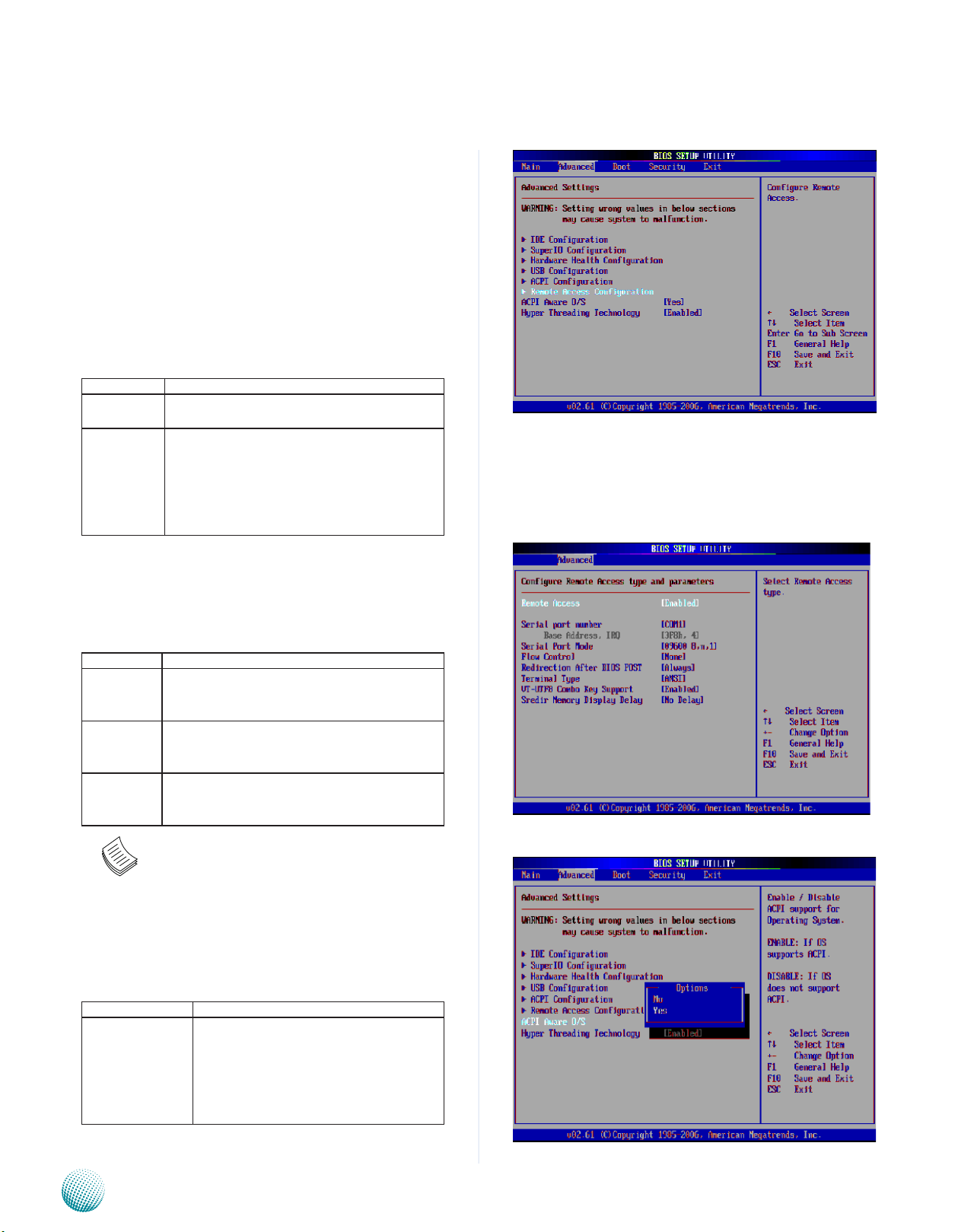
Remote Access Configuration
You can use this screen to select options for the Remote
Access Configuration. Use the up and down <Arrow> keys
to select an item. Use the <Plus> and <Minus> keys to
change the value of the selected option. The settings are
described on the followingpages. The screen is shown at
the right.
Remote Access
You can disable or enable the BIOS remote access feature
here.
Option Description
Disabled Set this value to prevent the BIOS from using
Remote Access..
Serial Set the value for this option to Serial to allow
the system to use the remote access feature.
The remote access feature requires a dedicated
serial port connection.
Bios Settings
Serial Port Number
Select the serial port you want to use for console
redirection. You can set the value for this option to either
COM1 or COM2.
Option Description
115200 8,n,1 Set this value to allow you to select 115200 as
the baud rate (transmitted bits per second) of
the serial port.
57600 8,n,1 Set this value to allow you to select 57600 as the
baud rate (transmitted bits per second) of the
serial port.
19200 8,n,1 Set this value to allow you to select 19200 as the
baud rate (transmitted bits per second) of the
serial port
Note: For instructions of setting up the remote
access on the client program, refer to Appendix B
Setting up the Remote Access.
ACPI Aware O/S
Option Description
No This setting should be set if the operating
system in use does not comply with the
ACPI (Advanced Configuration and Power
Interface) specification. DOS®, Windows
3.x®, and Windows NT® are examples of
non-ACPI aware operating systems.
Embedded and Industrial Computing
23
Page 27

Chapter 4
Yes This setting should be set if the operating
system complies with the ACPI (Advanced
Configuration and Power Interface)
specification. This is the default setting.
Windows 95®, Windows 98® and Windows
2000® are examples of ACPI aware operating
systems.
Hyper Threading Technology
Hyper-threading is an Intel-proprietary technology used to
improve parallelization of computations resulting in more
efficient use of processor resources. Enble this option for
the OS which supports Hyper Threading Technology and
disable this option for the OS which does no support the
Hyper Threading Technology.
Bios Settings
Embedded and Industrial Computing
24
Page 28

Chapter 4
Boot Settings
Select the Boot tab from the setup screen to enter the Boot
BIOS Setup screen. You can select any of the items in the
left frame of the screen, such as Boot Device Priority, to
go to the sub menu for that item. You can display an Boot
BIOS Setup option by highlighting it using the <Arrow>
keys.
Boot Settings Configuration
Select this tab to configure the preference of the booting
process such as the booting mode and the displayed
messages.
Boot Device Priority
Select this tab to specify the order in which the system
checks for the device to boot from.
Hard Disk Drives
Bios Settings
Select this tab to view the hard disk drives in the system.
Removable Drives
Select this tab to view the removable drives attached to
the system.
Embedded and Industrial Computing
25
Page 29

Chapter 4
Security Settings
Select Security Setup from the Setup main BIOS setup
menu. All Security Setup options, such as password
protection and virus protection, are described in this
section. To access the sub menu for the following items,
select the item and press <Enter>:
Supervisor Password
Indicates whether a supervisor password has been set. If
the password has been installed, Installed displays. If not,
Not Installed displays.
User Password
Indicates whether a user password has been set. If the
password has been installed, Installed displays. If not, Not
Installed displays.
Change Supervisor Password
Bios Settings
Select this option and press <Enter> to access the sub
menu. You can use the sub menu to change the supervisor
password.
Change User Password
Select this option and press <Enter> to access the sub
menu. You can use the sub menu to change the user
password.
Clear User Password
Select this option and press <Enter> to access the
sub menu. You can use the sub menu to clear the user
password.
Embedded and Industrial Computing
26
Page 30
Chapter 4
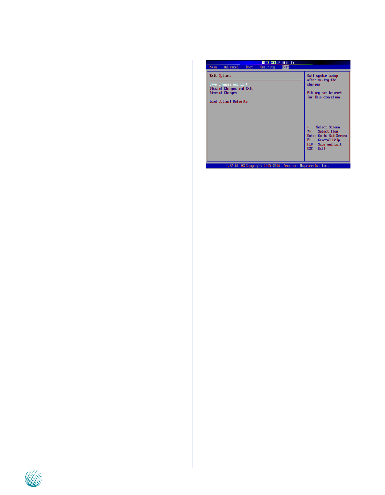
Exit Menu
Select the Exit tab from the setup screen to enter the Exit
BIOS Setup screen. You can display an Exit BIOS Setup
option by highlighting it using the <Arrow> keys. All Exit
BIOS Setup options are described in this section. The Exit
BIOS Setup screen is at right.
Exit Saving Changes
When you have completed the system configuration
changes, select this option to leave Setup and reboot the
computer so the new system configuration parameters
can take effect. Select Exit Saving Changes from the Exit
menu and press <Enter>.
Save Configuration Changes and Exit Now?
[Ok] [Cancel]
appears in the window. Select Ok to save changes and
exit.
Bios Settings
Exit Discarding Changes
Select this option to quit Setup without making any
permanent changes to the system configuration. Select
Exit Discarding Changes from the Exit menu and press
<Enter>.
Discard Changes and Exit Setup Now?
[Ok] [Cancel] appears in the window. Select Ok to discard
changes and exit.
Discard Changes
Select Discard Changes from the Exit menu and press
<Enter>.
Load Optimal Defaults
It automatically sets all Setup options to a complete set of
default settings when you Select this option. The Optimal
settings are designed for maximum system performance,
but may not work best for all computer applications. In
particular, do not use the Optimal Setup options if your
computer is experiencing system configuration problems.
Select Load Optimal Defaults from the Exit menu and
press <Enter>.
Embedded and Industrial Computing
27
Page 31

Appendix A
Programming Watchdog Timer
Appendix A: Programming Watchdog Timer
A watchdog timer is a piece of hardware that can be
used to automatically detect system anomalies and reset
the processor in case there are any problems. Generally
speaking, a watchdog timer is based on a counter that
counts down from an initial value to zero. The software
selects the counter’s initial value and periodically restarts
it. Should the counter reach zero before the software
restarts it, the software is presumed to be malfunctioning
and the processor’s reset signal is asserted. Thus, the
processor will be restarted as if a human operator had
cycled the power.
For sample watchdog code, see watchdog folder under
LEC-7100 Utility on the Driver and Manual CD
{
int temp, time;
if( argc < 2 )
{
help();
return -1;
}
if( strcmp(argv[1], “-wr”) == 0 )
{
if( argc != 3 )
{
help();
return -1;
}
write_w83627_reg(0x8, 0xf6, 0); //LDN=8, CRF6, stop
timer first
//clear status bit
Executing through the Command Line:
Execute the WD.EXE file under DOS (WD.EXE and CWSDPMI.
EXE should be placed on same directory), then enter the
values from 0~255. The system will reboot automatically
according to the time-out you set.
Watch Dog sample code:
#include <stdio.h>
#include <string.h>
#include <dos.h>
#include <stdlib.h>
#include <inlines/pc.h>
#define INDEX_PORT 0x2e
#define DATA_PORT 0x2f
void help()
{
printf(“Watchdog timer control for EM-9345\n\n”);
printf(“wd.exe -wr xxx (1-255 sec)(Watchdog Control SYSTEM RESET)\n”);
printf(“\n”);
}
int main(int argc, char *argv[])
write_w83627_reg(0x8, 0xf7, read_w83627_reg(0x8, 0xf7)
& 0xef);
time = atoi(argv[2]);
printf(“Setting Watchdog timer for System Reset...\n”);
set_watchdog(time);
return 0;
}
else
{
help();
return -1;
}
return 0;
}
int set_watchdog(int time)
{
int temp;
outportb(INDEX_PORT, 0x87);
delay(1);
outportb(INDEX_PORT, 0x87); //Entering
W83627HF Configuration
temp = read_w83627_reg(0, 0x2b); //LDN=0, CR2B
Embedded and Industrial Computing
temp &= 0xf3;
28
Page 32

Appendix A
Programming Watchdog Timer
temp |= 0x04;
write_w83627_reg(0, 0x2b, temp); //set watchdog pin
write_w83627_reg(0x8, 0xf6, 0); //LDN=8, CRF6, stop
timer first
write_w83627_reg(0x8, 0xf5, read_w83627_reg(0x8, 0xf5)
& 0xf7); //;set
second
write_w83627_reg(0x8, 0xf7, read_w83627_reg(0x8, 0xf7)
& 0xef); //;clear
status
write_w83627_reg(0x8, 0x30, read_w83627_reg(0x8,
0x30) | 0x01); //;enable
LDN8
temp = time;
write_w83627_reg(0x8, 0xf6, temp); //LDN=8, CRF6, set
watchdog timer time-out value
outportb(INDEX_PORT, 0xaa); //Exit W83627HF
Configuration
{For sample watchdog code, see watchdog folder on the
Driver and Manual CD
return 0;
}
int read_w83627_reg(int LDN, int reg)
{
outportb(INDEX_PORT, 0x07); //LDN register
delay(1);
outportb(DATA_PORT, LDN);
delay(1);
outportb(INDEX_PORT, reg);
delay(1);
return inportb(DATA_PORT);
}int write_w83627_reg(int LDN, int reg, int value)
{
outportb(INDEX_PORT, 0x07); //LDN register
delay(1);
outportb(DATA_PORT, LDN);
delay(1);
outportb(INDEX_PORT, reg);
delay(1);
outportb(DATA_PORT, value);
return 0;
}
Embedded and Industrial Computing
29
Page 33

Appendix B
Appendix B: Setting up Remote Access
Remote Access lets you monitor and configure a system
from a remote terminal computer by re-directing
keyboard input and text output through the serial port.
This following steps illustrate how to use this feature.
Connect one end of the console cable to console port 1.
of the system and the other end to serial port of the
Remote Client System.
Configure the following settings in the BIOS Setup 2.
menu for LEC-7100:
BIOS > Advanced > Remote Access Configuration >
Serial Port Mode > [9600, 8 , n ,1 ]
Configure Console Redirection on the client system. 3.
The following illustration is an example on Windows
platform:
Setting up Remote Access
A. Click the start button, point to Programs > a.
Accessories > Communications and select Hyper
Terminal.
B. Enter any name for the new connection and b.
select any icon.
Click OK.c.
From the “Connect to”. Pull-down menu, select the d.
appropriate Com port on the client system and
click OK.
Select 9600 for the Baud Rate, None. for Flow e.
contorl, 8 for the Data Bit, None for Parity Check,
and 1 for the Stop Bit.
Note: You will have to enable and configure
this feature on the BIOS. Please refer to Remote
Access on Chapter 4 BIOS Settings.
Embedded and Industrial Computing
30
Page 34

Appendix C
Digital Input/Output Control
Appendix C: Digital Input/Output Control on the GPIO port
The Digitanl I/O on the rear panel is designed to provide
the input and output operations for the system. For
sample DIO code, see 4bit-DIO folder under LEC-7100
Utility on the Driver and Manual CD.
A DIO sample code:
#include <stdio.h>
#include <dos.h>
/* This program assume 4 Input and 4 output */
/* Digital Input=GP24,25,26,27==> mapping to OUT0~3
*/
/* Digital Output=GP60,61,62,63 ==> mapping to IN0~3
*/
#define SUPERIO_INDEX 0x2e
#define SUPERIO_DATA 0x2f
#define BANK_REG 0x07
#define GPIO0 0x01
#define GPIO1 0x02
#define GPIO2 0x04
#define GPIO3 0x08
#define GPIO4 0x10
#define GPIO5 0x20
#define GPIO6 0x40
#define GPIO7 0x80
int print_help(char *argv[])
{
printf(“using: %s [i/o] [value]\n”, argv[0]);
printf(“Note:all data in hexadecimal format\n”);
printf(“eg: %s i ==>read Digital Input pin(3 2 1 0)\n”);
printf(“ %s o 8 ==>write 1000 to Output pin(3 2 1 0)\n”);
printf(“ %s o 0 ==>write 0000 to Output pin(3 2 1 0)\n”);
printf(“ %s o f ==>write 1111 to Output pin(3 2 1 0)\n”);
printf(“Program terminated !!!\n”);
exit(1);
}
void enter_sio_config()
{
outportb(SUPERIO_INDEX, 0x87);
delay(1); //delay some time
outportb(SUPERIO_INDEX, 0x87);
}
void exit_sio_config()
{
outportb(SUPERIO_INDEX, 0xaa);
}
unsigned char read_sio_reg(unsigned char bank_no,
unsigned char reg_no)
{
unsigned char reg_data;{
enter_sio_config();
outportb(SUPERIO_INDEX, BANK_REG);
delay(1);
outportb(SUPERIO_DATA, bank_no);
delay(1);
outportb(SUPERIO_INDEX, reg_no);
delay(1);
reg_data=inportb(SUPERIO_DATA);
exit_sio_config();
return reg_data;
}
void write_sio_reg(unsigned char bank_no, unsigned char
reg_no, unsigned char
write_data)
{
enter_sio_config();
outportb(SUPERIO_INDEX, BANK_REG);
delay(1);
outportb(SUPERIO_DATA, bank_no);
delay(1);
outportb(SUPERIO_INDEX, reg_no);
delay(1);
outportb(SUPERIO_DATA, write_data);
exit_sio_config();
}
unsigned char Get_DIO_Input_value()
Embedded and Industrial Computing
31
Page 35

Appendix C
Digital Input/Output Control
{
unsigned char temp1;
temp1 = (read_sio_reg(0x08,0xE5) & 0x0F);
return temp1;
}
void Set_DIO_Output_value(unsigned char temp1)
{
write_sio_reg(0x09,0xE5, (read_sio_reg(0x09,0xE5) &
0x0F) | temp1);
}
void Init_GPIO(void) {
write_sio_reg(0x09,0x30,0x02); //;enable GPIO2
function
write_sio_reg(0x08,0x30,0x04); //;enable GPIO6
function
write_sio_reg(0x09,0xE4,(read_sio_reg(0x09,0xE4) &
~(GPIO4+GPIO5+GPIO6+GPIO7))); //;set
GPI024,25,26,27=output
write_sio_reg(0x08,0xE4,(read_sio_reg(0x08,0xE4) |
(GPIO0+GPIO1+GPIO2+GPIO3))); //;set
GPI060,61,62,63=input
}
main(int argc, char *argv[])
{
int io_mode; //0: read 1:write
char *ptr;
unsigned char tmp;
unsigned char Input_value, Output_value;
printf(“===================================
============\n”);
printf(“ Digital IO test program for LEB-2010I Ver:1.0\n” );
printf(“===================================
============\n”);
Init_GPIO();
if ((argc<2)||(argc>4))
{
print_help(argv); //;The parameter over or not enough
}
if((*argv[1]==’i’)|(*argv[1]==’I’)) {
io_mode=0; //;0 for read
} else {
if((*argv[1]==’o’)|(*argv[1]==’O’)) {
io_mode=1; //;1 for write
// try to get the value which want to be write
ptr=argv[2];
tmp=*ptr;
switch (tmp)
{
case ‘0’:
Output_value = 0;
break;
case ‘1’:
Output_value = 1;
break;
case ‘2’:
Output_value = 2;
break;
case ‘3’:
Output_value = 3;
break;
case ‘4’:
Output_value = 4;
break;
case ‘5’:
Output_value = 5;
break;
case ‘6’:
Output_value = 6;
break;
case ‘7’:
Output_value = 7;
break;
case ‘8’:
Output_value = 8;
break;
case ‘9’:
Output_value = 9;
break;
Embedded and Industrial Computing
32
Page 36

Appendix C
Digital Input/Output Control
case ‘a’:
case ‘A’:
Output_value = 10;
break;
case ‘b’:
case ‘B’:
Output_value = 11;
break;
case ‘c’:
case ‘C’:
Output_value = 12;
break;
case ‘d’:
case ‘D’:
Output_value = 13;
break;
case ‘e’:
printf(“ write done...\n”);
}
}
case ‘E’:
Output_value = 14;
break;
case ‘f’:
case ‘F’:
Output_value = 15;
break;
default:
print_help(argv);
}
}
else {
print_help(argv);
}
}
if(io_mode==0) {
Input_value = Get_DIO_Input_value();
printf(“ The Input pin of Digital IO = 0x%x\n”, Input_
value);
} else {
Set_DIO_Output_value(Output_value <<4); // use bit3~0
map to GPO24~27
Embedded and Industrial Computing
33
Page 37

Appendix D
Terms and Conditions
Appendix D: Terms and Conditions
Warranty Policy
All products are under warranty against defects in 1.
materials and workmanship for a period of one year
from the date of purchase.
The buyer will bear the return freight charges for 2.
goods returned for repair within the warranty period;
whereas the manufacturer will bear the after service
freight charges for goods returned to the user.
The buyer will pay for repair (for replaced components 3.
plus service time) and transportation charges (both
ways) for items after the expiration of the warranty
period.
If the RMA Service Request Form does not meet the 4.
stated requirement as listed on “RMA Service,” RMA
goods will be returned at customer’s expense.
The following conditions are excluded from this 5.
warranty:
RMA Service
Requesting a RMA#
To obtain a RMA number, simply fill out and fax the 6.
“RMA Request Form” to your supplier.
The customer is required to fill out the problem code 7.
as listed. If your problem is not among the codes listed,
please write the symptom description in the remarks
box.
Ship the defective unit(s) on freight prepaid terms. 8.
Use the original packing materials when possible.
Mark the RMA# clearly on the box. 9.
Note: Customer is responsible for shipping
damage(s) resulting from inadequate/loose
packing of the defective unit(s). All RMA# are valid
for 30 days only; RMA goods received after the
effective RMA# period will be rejected.
Improper or inadequate maintenance by the customer
Unauthorized modification, misuse, or reversed
engineering of the product Operation outside of the
environmental specifications for the product.
Embedded and Industrial Computing
34
Page 38

Appendix D
RMA Service Request Form
When requesting RMA service, please fill out the following form. Without
this form enclosed, your RMA cannot be processed.
RMA No:
Reasons to Return: Ŀ Repair(Please include failure details)
Ŀ Testing Purpose
Company: Contact Person:
Phone No. Purchased Date:
Fax No.: Applied Date:
Return Shipping Address:
Shipping by: Ŀ Air Freight Ŀ Sea Ŀ Express ___
Ŀ Others:________________
Item Model Name Serial Number Configuration
Item Problem Code Failure Status
*Problem Code:
01:D.O.A.
02: Second Time
R.M.A.
03: CMOS Data Lost
04: FDC Fail
05: HDC Fail
06: Bad Slot
07: BIOS Problem
08: Keyboard Controller Fail
09: Cache RMA Problem
10: Memory Socket Bad
11: Hang Up Software
12: Out Look Damage
13: SCSI
14: LPT Port
15: PS2
16: LAN
17: COM Port
18: Watchdog Timer
19: DIO
20: Buzzer
21: Shut Down
22: Panel Fail
23: CRT Fail
24: Others (Pls specify)
Request Party
Confirmed By Supplier
Authorized Signature / Date Authorized Signature / Date
Terms and Conditions
Embedded and Industrial Computing
35
 Loading...