

Page 1

LEC-5510
Manual
Page 2

LEC-5510
Manual
© Copyright 2007, Lanner Electronics, Inc. All rights reserved. This document
contains proprietary information that is protected by copyright. No part of this
document may be reproduced, transmitted, transcribed, stored in a retrieval
system, or translated into any language in any form by any means without the
written express of Lanner Electronics, Inc.
The author and Lanner Electronics, Inc. have used their best efforts in preparing
this manual. However, the author and Lanner Electronics, Inc. make no
warranties of any kind, expressed or implied, with regard to the informational
content, documentation, or files contained in this manual, and shall not be liable
Page 3

for technical or editorial errors or omissions contained herein. In no event shall
the author or publisher be responsible or liable for any incidental or consequential
damages resulting from the furnishing, performance, or use of this material.
TRADEMARKS Internet Explorer, Windows Explorer, and Windows are trademarks
or registered trademarks of Microsoft Corporation. Other products mentioned
herein may be trademarks/or registered trademarks of their respective owners.
Page 4

Safety Guidelines
Follow these guidelines to ensure general safety:
Keep the chassis area clear and dust-free during and after installation.
Do not wear loose clothing or jewelry that could get caught in the chassis.
Fasten your tie or scarf and roll up your sleeves.
Wear safety glasses if you are working under any conditions that might be
hazardous to your eyes.
Do not perform any action that creates a potential hazard to people or makes
the equipment unsafe.
Disconnect all power by turning off the power and unplugging the power cord
before installing or removing a chassis or working near power supplies
Do not work alone if potentially hazardous conditions exist.
Never assume that power is disconnected from a circuit; always check the
circuit.
Operating Safety
Electrical equipment generates heat. Ambient air temperature may not be
adequate to cool equipment to acceptable operating temperatures without
adequate circulation. Be sure that the room in which you choose to operate
your system has adequate air circulation.
Ensure that the chassis cover is secure. The chassis design allows cooling air
to circulate effectively. An open chassis permits air leaks, which may
interrupt and redirect the flow of cooling air from internal components.
Electrostatic discharge (ESD) can damage equipment and impair electrical
circuitry. ESD damage occurs when electronic components are improperly
handled and can result in complete or intermittent failures. Be sure to follow
ESD-prevention procedures when removing and replacing components to avoid
these problems.
Wear an ESD-preventive wrist strap, ensuring that it makes good skin contact.
If no wrist strap is available, ground yourself by touching the metal part of the
chassis.
Page 5

Periodically check the resistance value of the antistatic strap, which should be
between 1 and 10 megohms (Mohms).
Page 6

EMC Notice
This equipment has been tested and found to comply with the limits for a Class A
digital device, pursuant to Part 15 of the FCC Rules. These limits are designed to
provide reasonable protection against harmful interference when the equipment
is operated in a commercial environment. This equipment generates, uses, and
can radiate radio frequency energy and, if not installed and used in accordance
with the instruction manual, may cause harmful interference to radio
communications. Operation of this equipment in a residential area is likely to
cause harmful interference in which case users will be required to correct the
interference at their own expense.
Class A Notice for FCC
Modifying the equipment without the authorization of Lanner Electronics, Inc.
may result in the equipment no longer complying with FCC requirements for Class
A digital devices. In that event, your right to use the equipment may be limited by
FCC regulations, and you may be required to correct any interference to radio or
television communications at your own expense.
This equipment is in compliance with the essential requirements and other
relevant provisions of Directive 1999/5/EC.
Page 7

Contents
Safety Guidelines....................................................................................... 4
EMC Notice................................................................................................. 6
Contents .................................................................................................... 7
1. Product Overview ................................................................................. 8
1.1 Product Introduction ....................................................................... 8
1.2 Features and Benefits ...................................................................... 8
1.3 Specifications................................................................................. 10
1.4 Block Diagram................................................................................ 11
1.5 Package Contents ............................................................. 11
1.6 Technical Assistance...................................................................... 11
2. System Components ........................................................................... 13
2.1 LEC-5510 System Board ................................................................. 13
2.1.1 Board Layout............................................................................... 14
2.2 Jumper Settings and I/O Connectors............................................ 14
2.1.3 Connector Pin Assignments........................................................ 15
2.2 Mechanisms .................................................................. 23
2.2.1 Front Panel LED Status and Behavior......................................... 23
2.2.2 Rear View.......................................................................... 25
B. Appendix B: Watchdog Timer............................................................. 29
B.1 Introduction .................................................................................. 29
C. Terms and Conditions.......................................................................... 30
Page 8
1. Product Overview
1.1 Product Introduction
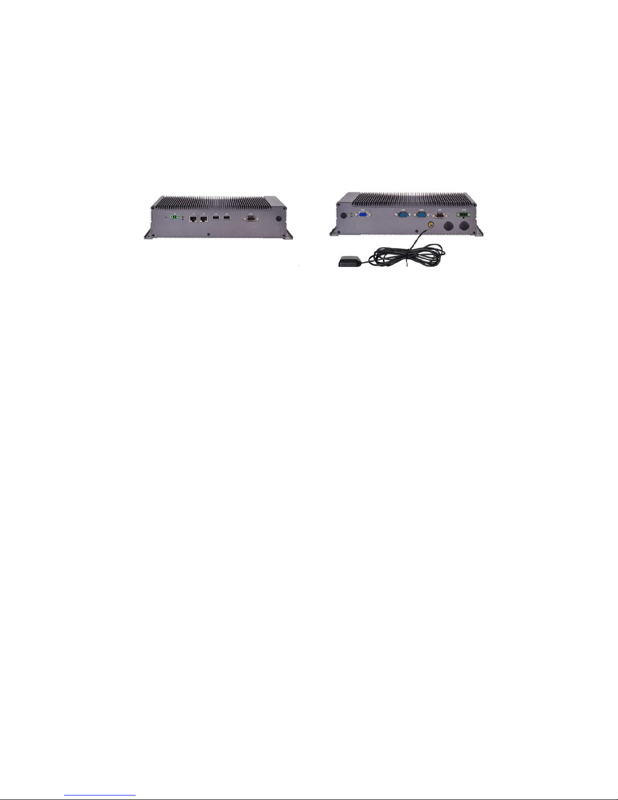
Figure 1 – LEC-5510 Outlook
In-Vehicle Fanless Embedded Box with Intel Dual Core Atom D51O CPU, 1GB
DDR2 Memory and GPS on board. Support 6~30VDC power input and Power
Ignition Control. Dual Intel GbE, VGA, COMx2, Audio, TTL DIO, USBx4, CFx1 and
2.5" SATA HDD support.
1.2 Features and Benefits
Listed below are the key features of LEC-5510:
Onboard Intel Dual Core Atom D510
Onboard 1GB memory
Power ignition control mechanism provided by programmable on/off/delay
switch circuit.
Battery voltage protection: OVP (Over Voltage Protection) and UVP (Under
Voltage Protection) circuit
Storage anti-vibration protection: Anti-vibration bracket is provided to
protect CF & Hard Drive.
Onboard GPS receiver for vehicle tracking and navigation system.
Dual Mini PCIe with SIM card socket for HSPA communication (3G) and Wi-Fi
or Bluetooth.
Page 9

One PCI-104 connector for easy expansion, such as Video Grabber or CAN
Bus modules.
Fanless and low power consumption
Extended operating temperature between -20ºC ~ 55 ºC
Wide range of DC power input from 6V to 30V.
I/O ports: RS-232/422/485, 2 LAN ports, 4 USB ports, VGA, Digital
input/output ports
Onboard 3-axis digital accelerometer (G Sensor) Multiple Antenna options
Page 10
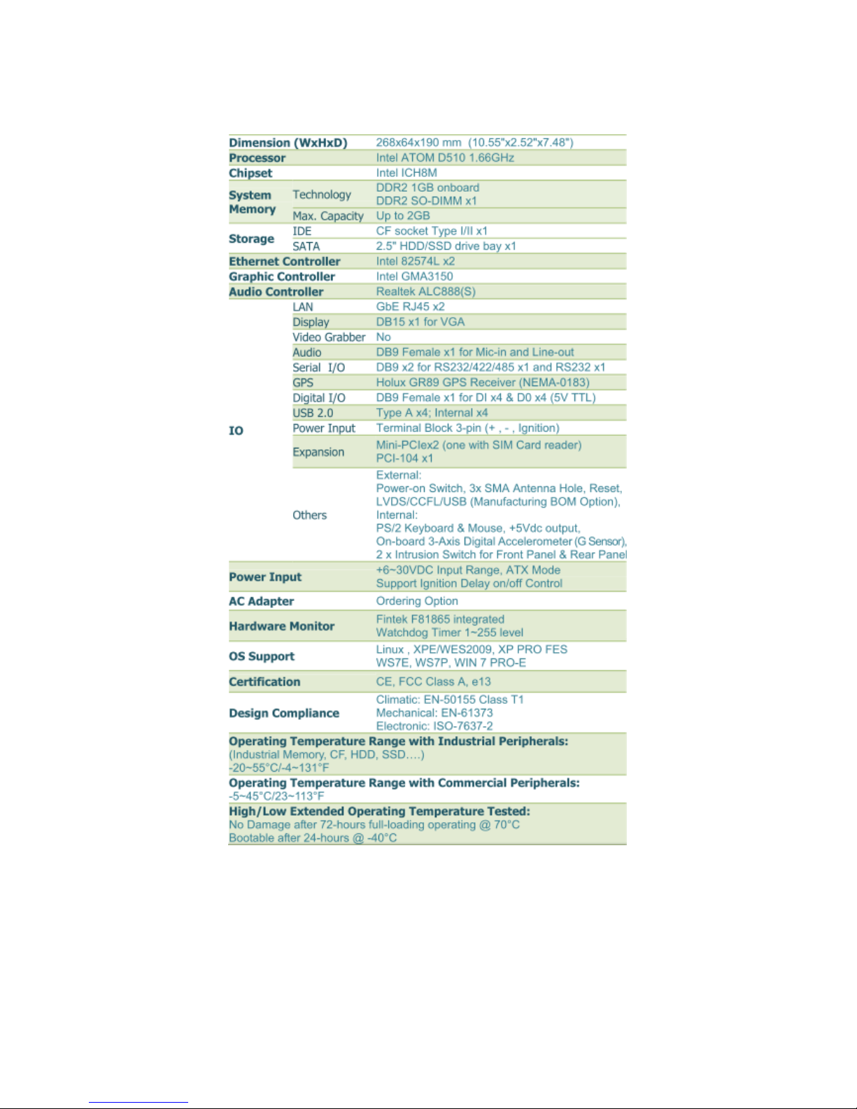
1.3 Specifications
Page 11
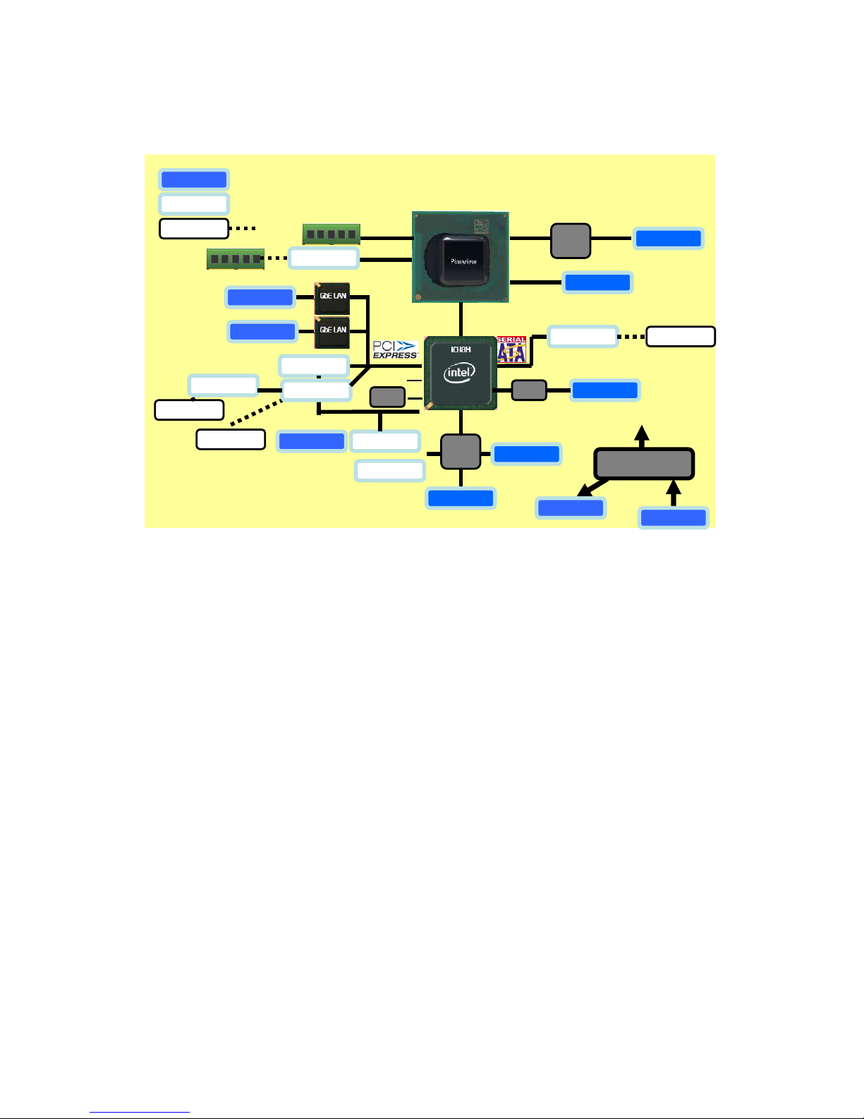
1.4 Block Diagram
VGA
Mini-PCIexpress
RJ45
M12
Flash
BIOS
SPI
USB
USB x4 USB x2
SATA x2
2.5” HDD
Super
I/O
LPC
RS232/422/485 x2
RS232 x2
Ignition Power Module
Intel D510
+6-35V DC-in
Edge I/O
Internal I/O
DDR2
SO-DIMM x1
WiFi or 3G
module
SIM Card for 3G
Option Module
DVI-D
Transmitter
18-bit
LVDS
1GB Memory
DIO
SPI
Mini-PCIexpress
SIM Card
Socket
+12/+5V DC-Out
ALC888
Audio
+12V
VGA
Mini-PCIexpress
RJ45
M12
Flash
BIOS
SPI
USB
USB x4 USB x2
SATA x2
2.5” HDD
Super
I/O
LPC
RS232/422/485 x2
RS232 x2
Ignition Power Module
Intel D510
+6-35V DC-in
Edge I/O
Internal I/O
DDR2
SO-DIMM x1
WiFi or 3G
module
SIM Card for 3G
Option Module
DVI-D
Transmitter
18-bit
LVDS
1GB Memory
DIO
SPI
Mini-PCIexpress
SIM Card
Socket
+12/+5V DC-Out
ALC888
Audio
+12V
1.5 Package Contents
Carefully unpack your package and make sure that you have the following items.
LEC-5510 Fanless Embedded Box x 1
WALL MOUNT x 1
Drivers and User’s Manual CD x 1
2 pin Male Terminal Block x 1
3 pin Female Terminal Block x1
GPS ANTENNA CABLE x1
Note: If you should find any components missing or damaged, please contact your dealer immediately for
assistance.
1.6 Technical Assistance
Page 12

Should you have any questions or problems with your product, please contact the
Lanner sales team.
Phone: 886-2-8692-6060
Fax: 886-2-8692-6101
E-mail: [email protected]
Prior to contacting us, we ask that you first check the electronic product
documentation for assistance. Should you still have questions, we recommend
you have the following information on hand in order to expedite the process:
LEC-5510 model name
Part number
Local network configuration details
Abnormal behavior and/or error messages reported by your network system
Your questions, or a description of the problem you are experiencing
Page 13
2. System Components
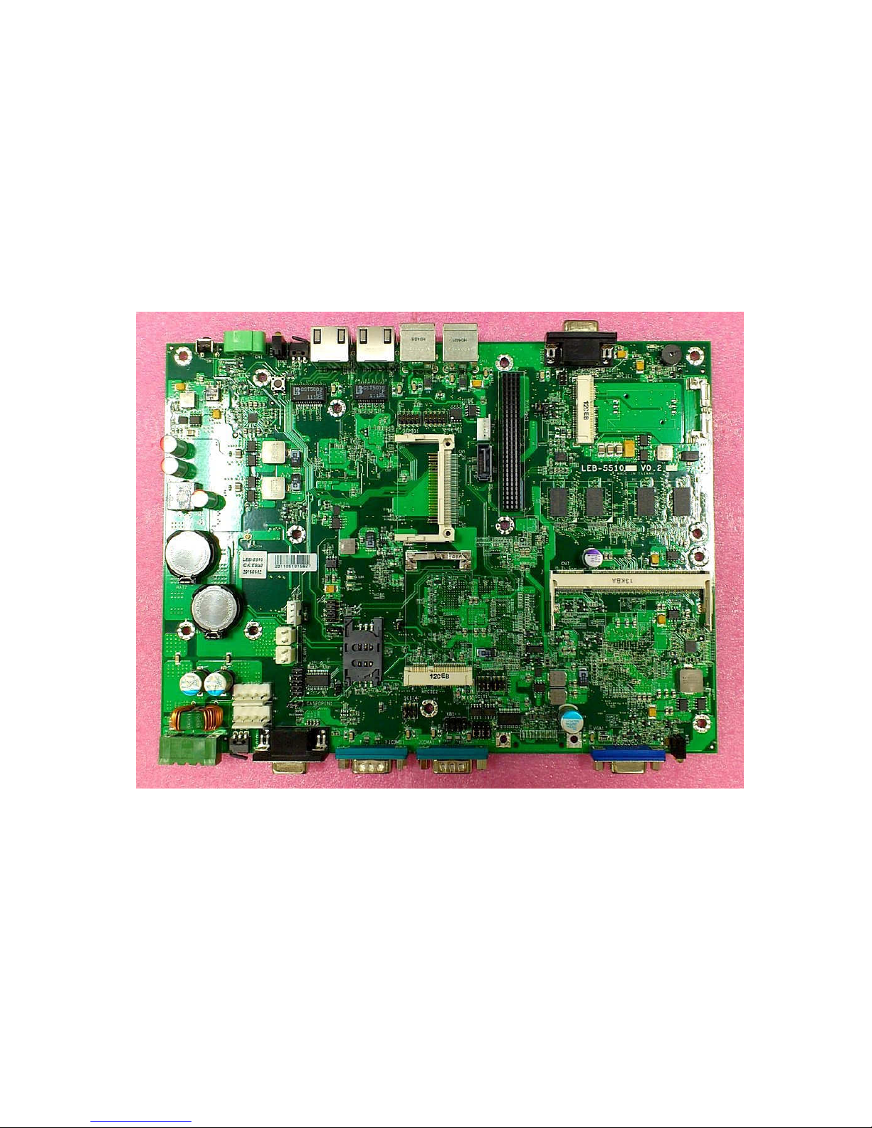
2.1 LEC-5510 System Board
LEB-5510 is the system board bundled with the LEC-5510 In-Vehicle Fanless
Embedded Box. The succeeding sections list LEB-5510 related jumper settings
and connector pin assignments.
Figure 2 – LEB-5510 Motherboard
Page 14
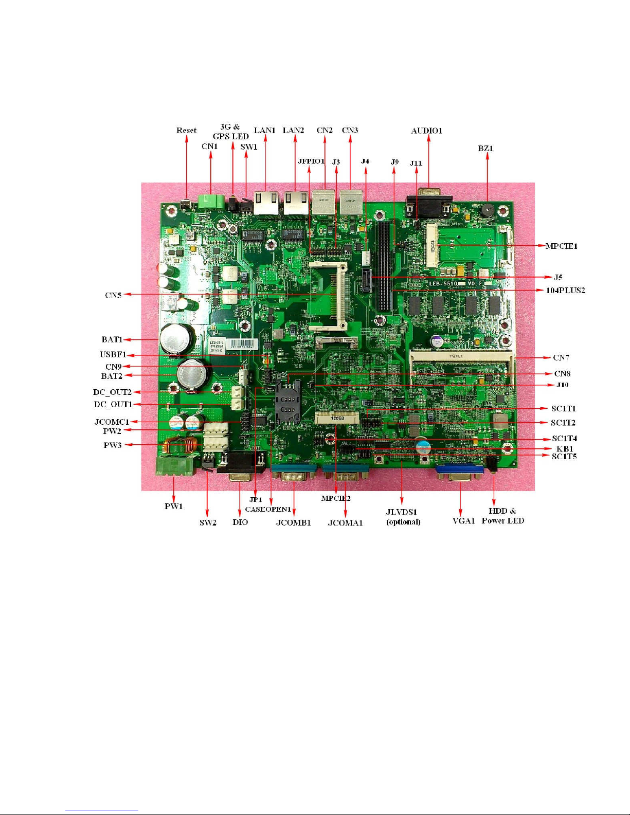
2.1.1 Board Layout
Figure 3 – LEB-5510 Jumpers and Connectors
2.2 Jumper Settings and I/O Connectors
The jumper settings and I/O connectors of the LEB-5510 board are specific to the
LEC-5510. Changing these settings may result in malfunctions or damages to
your system.
Page 15
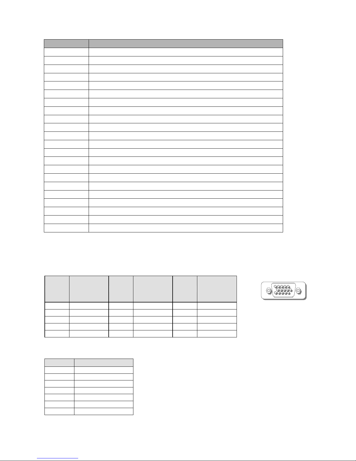
JUMPER FUNCTION
VGA1 DB-15 VGA Connector
J1 7 Pin 180º SATA CONNECTOR
J4 SATA POWER CONNECTOR
JCOMA1 COM1( D-SUB9) Connector
SC1T5/SC1T1 Function Selector for JCOMA1
SC1T2 Pin-9 Voltage Selector for JCOMA1
JCOMB1 COM2( D-SUB9) Connector
SC1T4 Pin-9 Voltage Selector for JCOMA2
JCOMC1 COM3( D-SUB9) Connector ( 2X5 Pin 2.0mm Header )
DIO1 Digital IN/OUT( D-SUB9 Female) Connector
JP1 Clear CMOS Data
CASEOPEN1 CASE OPEN FUNCTION
CN5 Compact Flash Connector
CN2/CN3 USB Dual Connector port#0/1
AUDIO1 AUDIO CONNECTOR (DB-9 Female)
KB1 PS/2 Keyboard & Mouse Connector (2x4 Header 2.54mm )
LAN1/LAN2 RJ-45 with LED
PW1 DC_IN CONNECTOR
PW2/PW3 EXT DC_IN Connector
CN1 POWER BUTTON
CN9 IGNITION CONTROL
DC_OUT1/2 Main board DC_IN Connector
2.1.3 Connector Pin Assignments
VGA1: Internal VGA Connector
Pin No.
Description
Pin No.
Description
Pin No.
Description
1 CRT-R 6 GND 11 N.C
2 CRT-G 7 GND 12 V_SDAT
3 CRT-B 8 GND 13 HSYNC
4 N.C 9 VCC 14 VSYNC
5 GND 10 GND 15 V_SCLK
J1:180º SATA CONNECTOR
PIN NO.
DESCRIPTION
1
GND
2
TX+
3
TX-
4
GND
5
RX-
6
RX+
7 GND
COM1(VGA)
5 1
Page 16

J4 SATA POWER CONNECTOR
PIN NO.
DESCRIPTION
1
N.C
2
GND
3
GND
4
+5V
Page 17
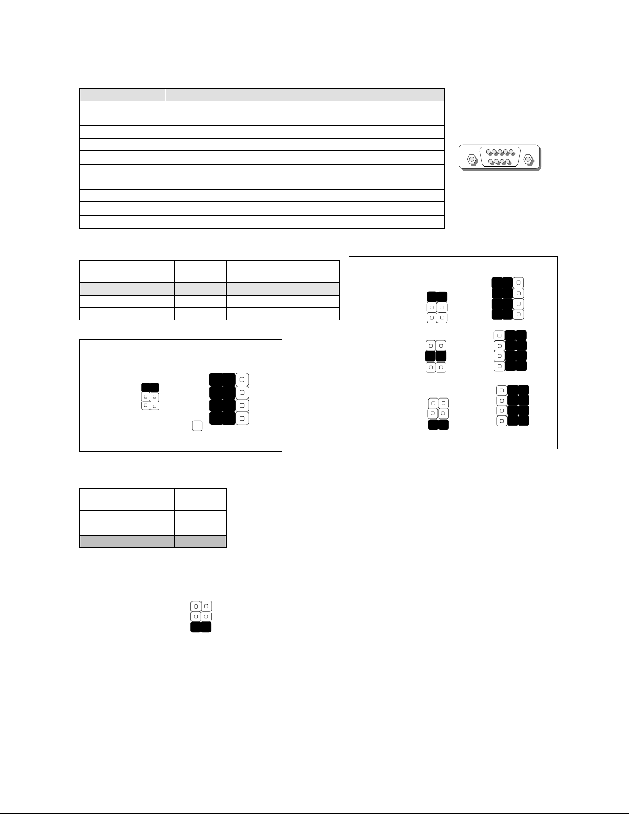
JCOMA1: COM1( D-SUB9) Connector
PIN NO. DESCRIPTION
RS-232 RS-422 RS-485
1 Data Carrier Detect ( DCDA # ) Tx- TxRx2 Receive Data ( RXDA ) Tx+ TxRx+
3 Transmit Data ( TXDA ) Rx-
4
Data Terminal Ready ( DTRA # ) Rx+
5 Ground ( GND )
6 Data Set Ready ( DSRA # )
7 Request To Send ( RTSA # )
8
Clear To Send ( CTSA # )
9 Ring Indicator ( RIA # )
SC1T5/SC1T1:Select COM1 Function
COM1 TYPE SC1T1 SC1T5
RS-232 (Default) 1-2 1-5,2-6,3-7,4-8
RS-422 3-4 5-9,6-10,7-11,8-12
RS-485 5-6 5-9,6-10,7-11,8-12
SC1T2:Select COM1 Pin9 Function
Pin 9 Function SC1T2
+5V 1-2
+12V 3-4
RI# 5-6
SC1T1
1
3
5
9
10
11
12
SC1T5
1
2
3
4
2
4
6
Default :
1
2
3
4
9
10
11
12
SC1T5
SC1T1
2
4
6
1
3
5
COM1
1 5
9 6
Default :
1
3
5
2
4
6
SC1T1
Page 18
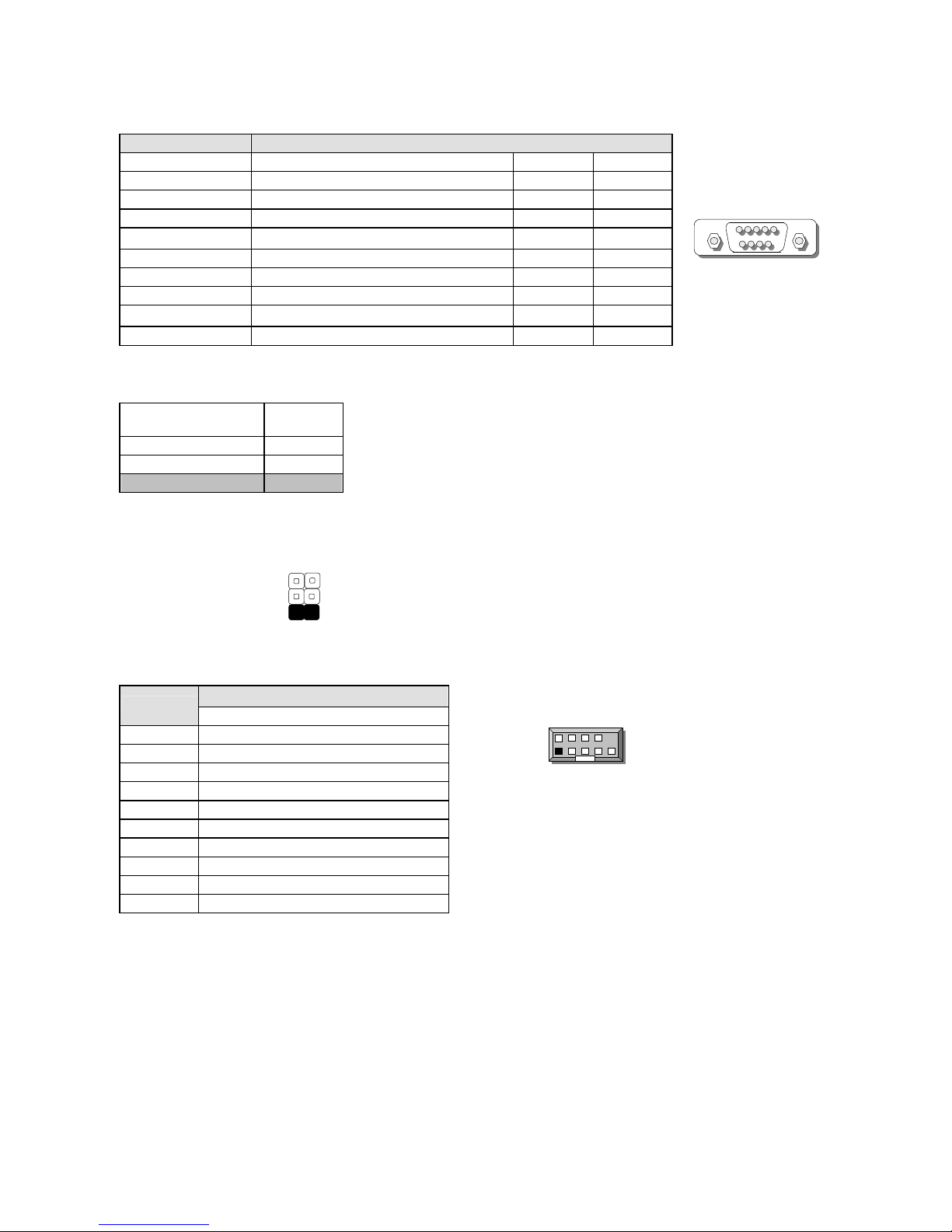
JCOMB1: COM2( D-SUB9) Connector
PIN NO. DESCRIPTION
RS-232
1 Data Carrier Detect ( DCDA # )
2 Receive Data ( RXDA )
3 Transmit Data ( TXDA )
4
Data Terminal Ready ( DTRA # )
5 Ground ( GND )
6 Data Set Ready ( DSRA # )
7 Request To Send ( RTSA # )
8
Clear To Send ( CTSA # )
9 Ring Indicator ( RIA # )
SC1T4:Select COM2 Pin9 Function
Pin 9 Function SC1T4
+5V 1-2
+12V 3-4
RI# 5-6
JCOMC1: COM2( D-SUB9) Connector ( 2X5 Pin 2.0mm
Header )
DESCRIPTION
PIN NO.
RS-232
1 Data Carrier Detect (DCDC #)
2 Data Set Ready (DSRC #)
3 Receive Data (RXDC)
4 Request To Send (RTSC #)
5 Transmit Data (TXDC)
6 Clear To Send (CTSC #)
7 Data Terminal Ready (DTRC #)
8 Ring Indicator (RIC #)
9 Ground
10 KEY
COM2
1 5
9 6
Default :
1
3
5
2
4
6
SC1T4
1
2
9
10
COM2
Page 19
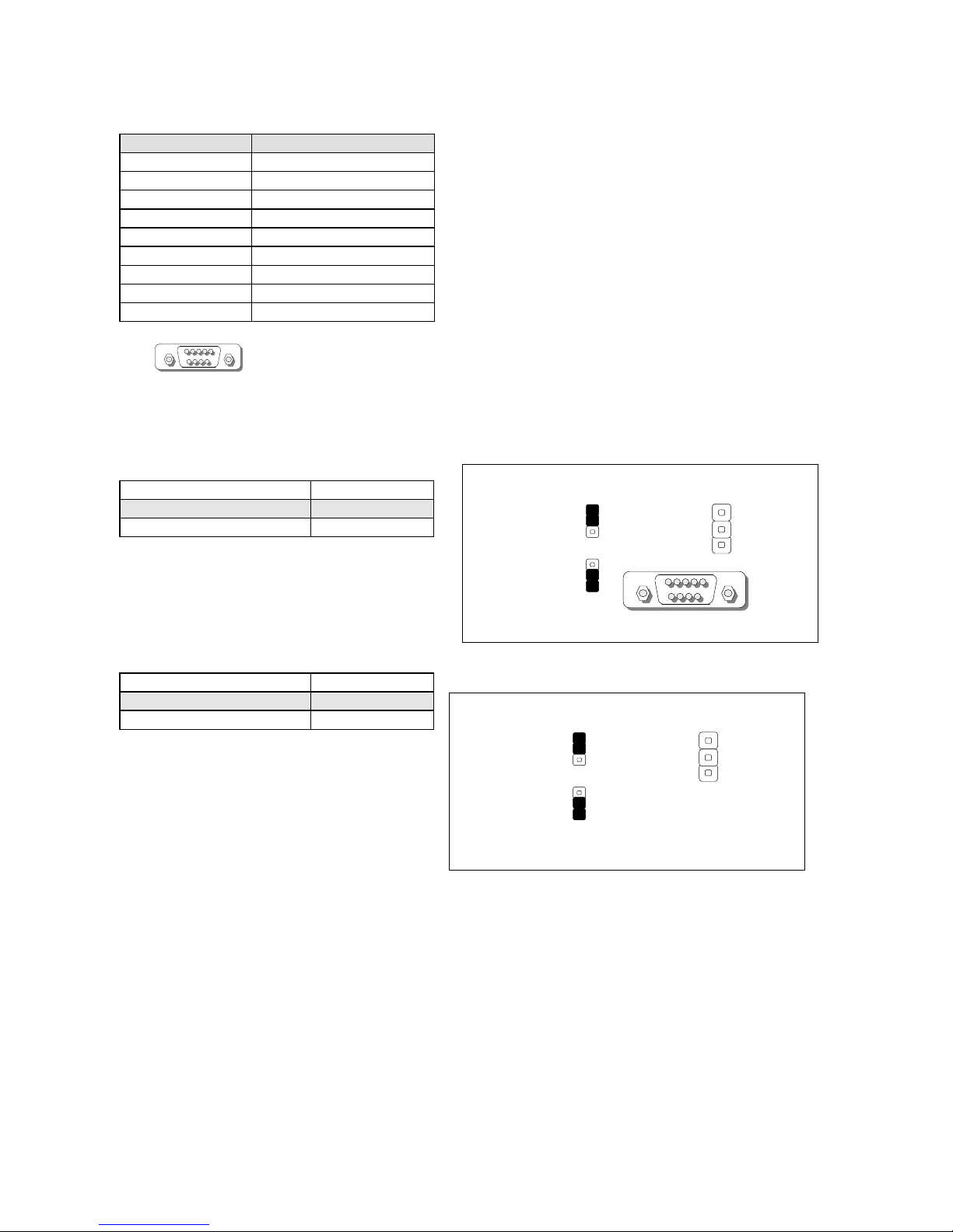
Enable
JP1
1
2
3
JP1
1
2
3
1
2
3
DIO1: Digital IN/OUT( D-SUB9 Female) Connector
PIN NO. DESCRIPTION
1 DO_1
2 DO_2
3 DO_3
4 DO_4
5 GND
6 DI_1
7 DI_2
8 DI_3
9 DI_4
JP1:Clear CMOS Data
Description CMOS1
Normal (Default) 1-2
Clear CMOS 2-3
CASEOPEN1:CASE OPEN FUNCTION
Description CMOS1
Disable(Default) 1-2
Enable 2-3
DIO1
1
6
Clear CMOS1
JP1
1
2
3
JP1
1
2
3
1
2
3
DIO1
1 5
9 6
Page 20
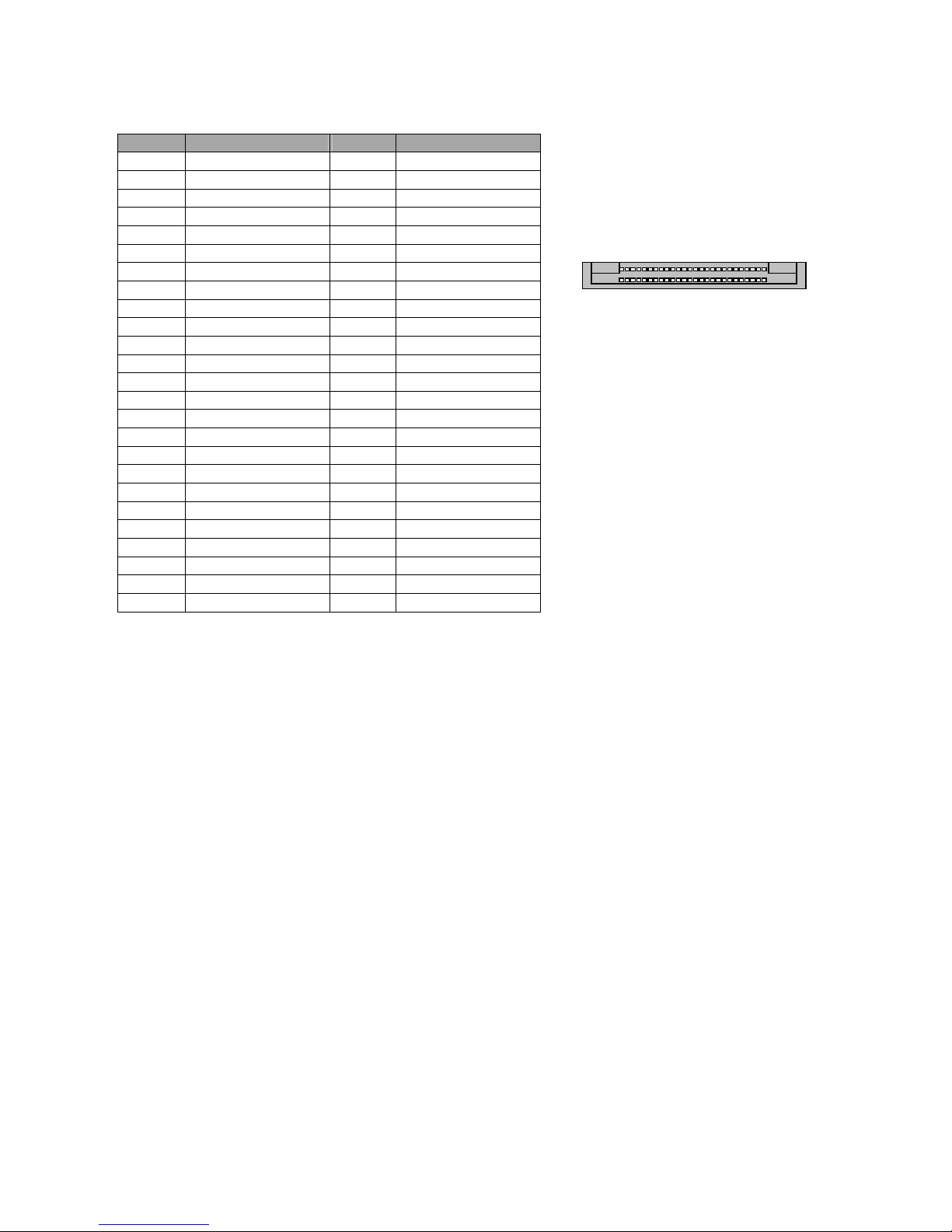
CN5: Compact Flash Connector
PIN DESCRIPTION PIN DESCRIPTION
1 GND 26 CD12 DATA3 27 DATA11
3 DATA4 28 DATA12
4 DATA5 29 DATA13
5 DATA6 30 DATA14
6 DATA7 31 DATA15
7 CE1# 32 CE2#
8 A10 33 VS1#
9 OE# 34 IOR#
10 A9 35 IOW#
11 A8 36 WE#
12 A7 37 READY#
13 CFVCC3 38 CFVCC3
14 A6 39 CSEL
15 A5 40 VS2#
16 A4 41 RESET
17 A3 42 WAIT#
18 A2 43 INPACK#
19 A1 44 REG#
20 A0 45 DASP#
21 DATA0 46 DIAG#
22 DATA1 47 DATA8
23 DATA2 48 DATA9
24 WP 49 DATA10
25 CD2- 50 GND
CN1
Page 21
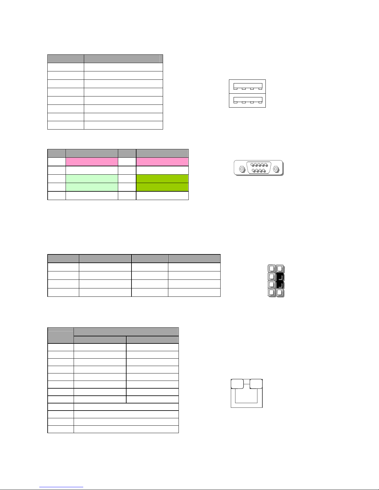
CN2/CN3::::USB Dual Connector port#0/1
PIN NO.
DESCRIPTION
1 5V_USB1
2 -USB0
3 +USB0
4 GND
5 5V_USB1
6 -USB1
7 +USB1
8 GND
AUDIO1 : AUDIO CONNECTOR (DB-9 Female)
PIN DESCRIPTION PIN DESCRIPTION
1 MIC_OUT_R 6 MIC_OUT_L
2 N.C 7 N.C
3 LINE_OUT_R 8 GND
4 LINE_OUT_L 9 GND
`5 N.C
KB1:PS/2 Keyboard & Mouse Connector (2x4 Header
2.54mm )
PIN NO. DESCRIPTION PIN NO. DESCRIPTION
1 VCC 2 MSCLK
3 MSDATA 4 KEY
5 KBDATA 6 KEY
7 GND 8 KBCLK
LAN1/LAN2: RJ-45 with LED
Description
Pin No.
Fast E-Net Giga Net
1 TX+ MD0+
2 TX- MD0
3 RX+ MD1+
4 T45 MD2+
5 T45 MD26 RX- MD17 T78 MD3+
8 T78 MD3-
9 10-/100-/1000+
10 10+/100+/100011 Link+/ACT12 Link-/ACT+
2
4
6
8
1
3
5
7
AUDIO1
1 5
9 6
USBB1
5 8
4
1
Page 22
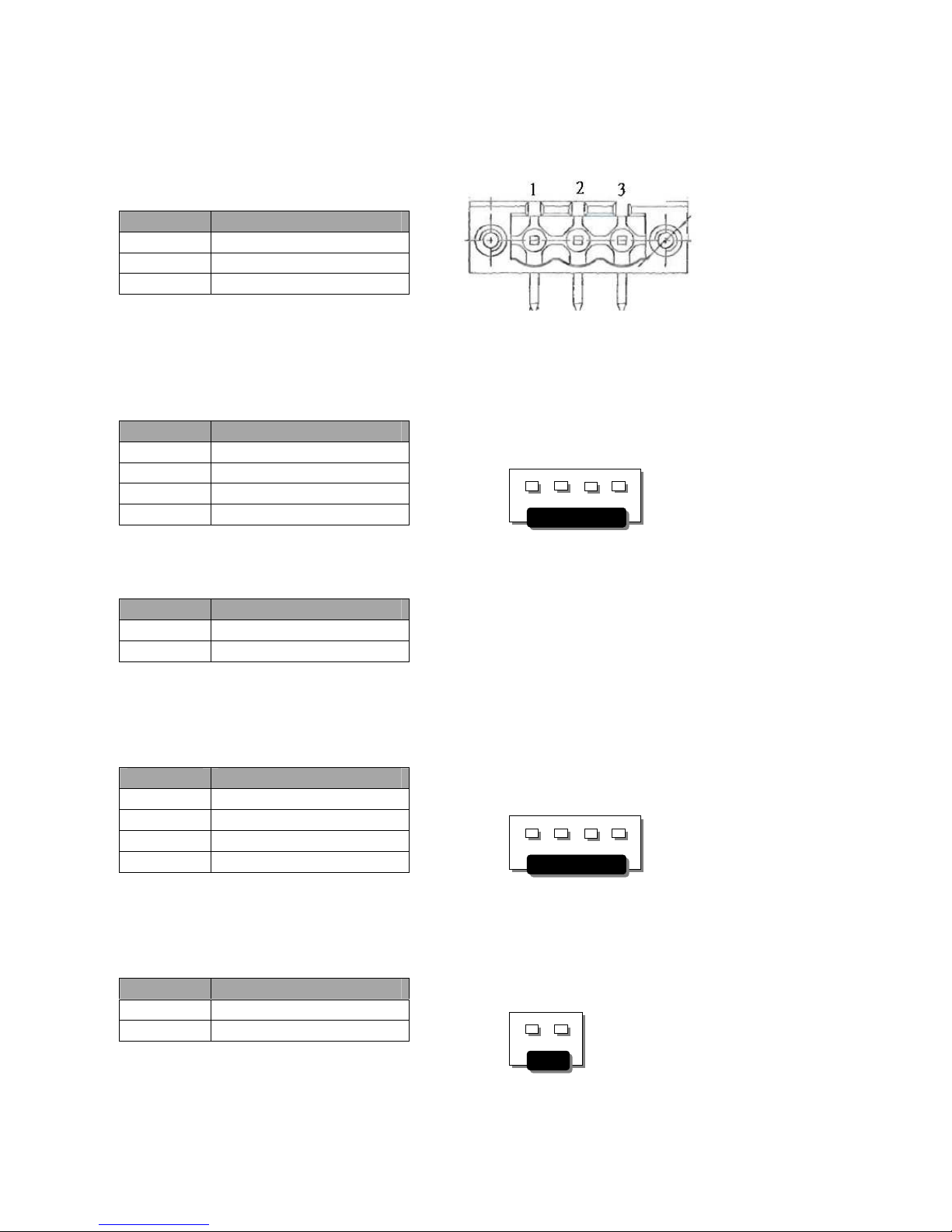
PW1 DC_IN CONNECTOR
PIN NO. DESCRIPTION
1 DC_GND
2 DC_IN
3 IGNITION
PW2/PW3 EXT DC_IN Connector
CN1::::POWER BUTTON
PIN NO. DESCRIPTION
1 POWER BUTTON
2 GND
CN9::::IGNITION CONTROL
DC_OUT1/2::::Main board DC_IN Connector
PIN NO. DESCRIPTION
1 DC_IN
2 DC_GND
3 IGNITION
4 N.C
PIN NO. DESCRIPTION
1 POWER_BTN
2 GND
3 POWER_OK
4 PS_ON#
PIN NO. DESCRIPTION
1 DC_IN
2 DC_GND
3
2
1
EXT DC_IN
4
2
1
DC_IN
3
2
1
EXT DC_IN
4
Page 23
LEC-5510
2.2 Mechanisms
This section of the manual describes the mechanical and device
nomenclature of the LEC-5510.
2.2.1 Front Panel LED Status and Behavior
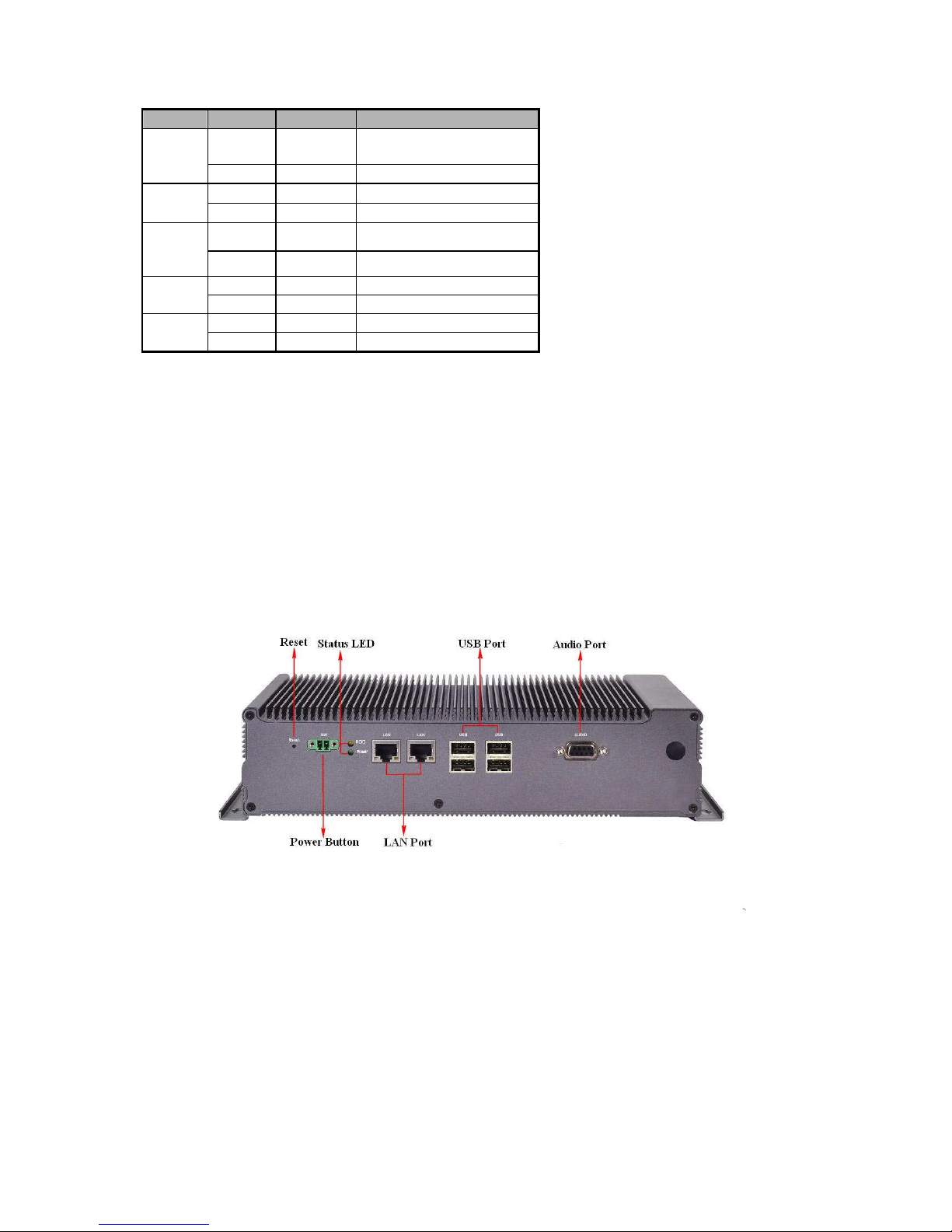
Figure 5 – LEC-5510 Front Panel
The following table provides a description of each LED on the LEC-5510’s
front panel:
Reset: Resetting LEC-5510 system
Power Button: Shutdown LEC-5510 system.
Status LED: Illustrating status of HDD and system power
LAN Port: Requires Ethernet RJ-45 cables to connect Ethernet networking
LED COLOR STATUS DESCRIPTION
Yellow
On Indicates when LEC-5510
power is switched ON PWR
N/A Off No power connected
Green
On Hard disk is being accessed
HDD
N/A
Off No data is being accessed
Green
On LAN is connected Ethernet
Ports
Link/ACT
Orange Flash data is being accessed
Yellow On GPS is actived
GPS
N/A Off GPS is inactived
Green On 3G is actived
3G
N/A Off GPS is inactived
Page 24

LEC-5510
USB Port: Providing 4 USB devices connection
Audio: Providing Microphone-in and Line-out audio connection
Page 25
LEC-5510
2.2.2 Rear View
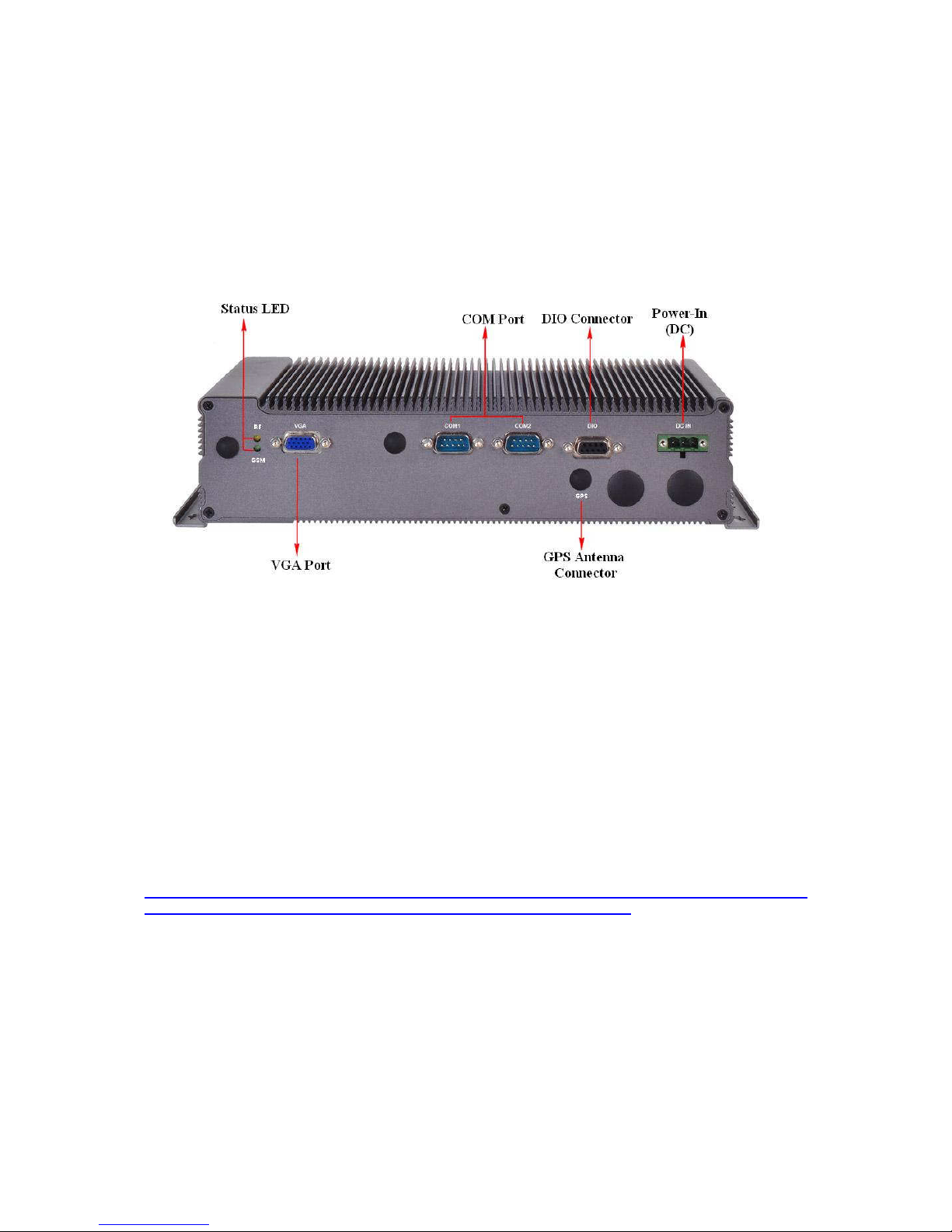
Figure 6 – FW-7890 Rear View
Status LED: Illustrating status of RF and GSM
VGA Port: Connecting to display monitor
COM1: Provide selectable RS485 or RS232 connection.
COM2: Provide RS232 connection.
GPS Antenna Connector: Connecting an antenna for build-in GPS
Power-In (DC): Power-in with ignition support. LEC-5510 support ether
+12V or +24V in-vehicle power system with wide range +6V ~ +30V.
Warning: Faulty or improper use of the power source may cause permanent damage to the
LEC-5510. Plug the terminal block that matches its specifications.
Page 26

LEC-5510
Page 27

LEC-5510
Page 28

LEC-5510
Page 29
LEC-5510
B. Appendix B: Watchdog Timer
B.1 Introduction
Most systems need to be self-reliant. If an error should occur it is typically
not possible to wait for the system to be rebooted manually. In some cases,
such as space probes, the system is simply not accessible to human
operators. If such systems should ever hang, they would be permanently
disabled. In other cases, the speed at which a human operator would reset
the system would be too slow to meet the uptime requirements of the
product.
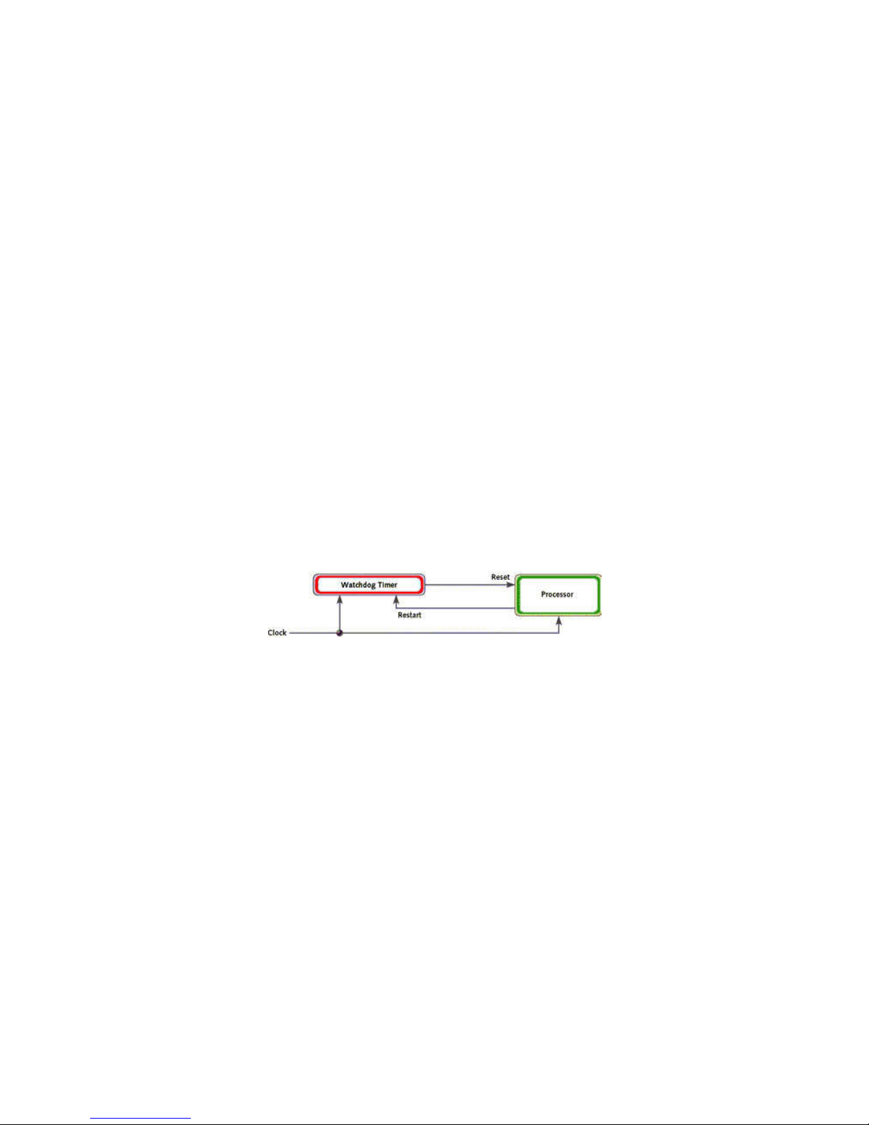
A watchdog timer is a piece of hardware that can be used to automatically
detect system anomalies and reset the processor in the case any problems
are found. Generally speaking, a watchdog timer is based on a counter that
counts down from an initial value to zero. The software selects the counter's
initial value and periodically restarts it. Should the counter reach zero
before the software restarts it, the software is presumed to be
malfunctioning, and the processor's reset signal is asserted. Thus, the
processor will be restarted as if a human operator had cycled the power.
Note: The watchdog function is from the Intel 6300ESB. Lanner provides sample code and the Intel
6300ESB datasheet in the manual/driver CD under the path: //WATCHDOG.
Page 30

LEC-5510
C. Terms and Conditions
Date:2007.03.19
Warranty Policy
1. All products are under warranty against defects in materials and workmanship for
a period of one year from the date of purchase.
2. The buyer will bear the return freight charges for goods returned for repair within
the warranty period; whereas the manufacturer will bear the after service freight
charges for goods returned to the user.
3. The buyer will pay for repair (for replaced components plus service time) and
transportation charges (both ways) for items after the expiration of the warranty
period.
4. If the RMA Service Request Form does not meet the stated requirement as listed
on “RMA Service,” RMA goods will be returned at customer’s expense.
5. The following conditions are excluded from this warranty:
Improper or inadequate maintenance by the customer
Unauthorized modification, misuse, or reversed engineering of the product
Operation outside of the environmental specifications for the product.
RMA Service
Requesting a RMA#
1. To obtain a RMA number, simply fill out and fax the “RMA Request Form” to your
supplier.
2. The customer is required to fill out the problem code as listed. If your problem is
not among the codes listed, please write the symptom description in the remarks box.
3. Ship the defective unit(s) on freight prepaid terms. Use the original packing
materials when possible.
4. Mark the RMA# clearly on the box.
Note: Customer is responsible for shipping damage(s) resulting from inadequate/loose packing of the
defective unit(s). All RMA# are valid for 30 days only; RMA goods received after the effective RMA#
period will be rejected.
Page 31
LEC-5510
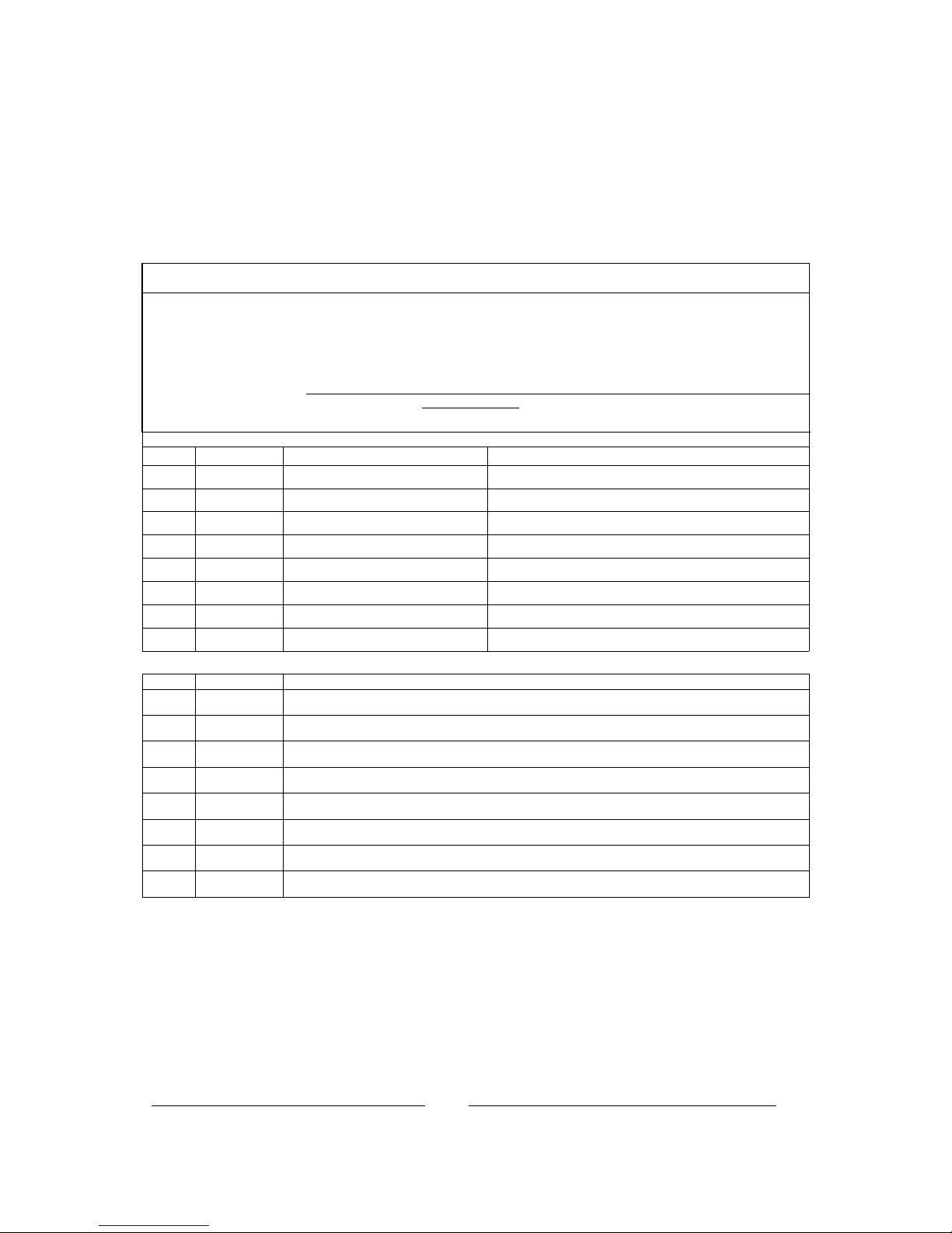
RMA Service Request Form
When requesting RMA service, please fill out the following form. Without
this form enclosed, your RMA cannot be processed.
RMA No:
Reasons to Return: □ Repair(Please include failure details)
□ Testing Purpose
Company: Contact Person:
Phone No. Purchased Date:
Fax No.: Applied Date:
Return Shipping Address:
Shipping by: □ Air Freight □ Sea □ Express ___
□ Others:________________
Item Model Name Serial Number Configuration
Item Problem Code Failure Status
*Problem Code:
01:D.O.A.
02: Second Time
R.M.A.
03: CMOS Data Lost
04: FDC Fail
05: HDC Fail
06: Bad Slot
07: BIOS Problem
08: Keyboard Controller Fail
09: Cache RMA Problem
10: Memory Socket Bad
11: Hang Up Software
12: Out Look Damage
13: SCSI
14: LPT Port
15: PS2
16: LAN
17: COM Port
18: Watchdog Timer
19: DIO
20: Buzzer
21: Shut Down
22: Panel Fail
23: CRT Fail
24: Others (Pls specify)
Request Party
Confirmed By Supplier
Authorized Signature / Date Authorized Signature / Date
 Loading...