

Page 1

Embedded &
Industrial Computing
Hardware Platforms for Embedded and Industrial Computing
LEC-3100
>>
User's Manual
Publication date:2011-05-10
Page 2

TTaTTable of Contentsbeable of Contents
Chapter 1: Introduction 1
System Specication . . . . . . . . . . . . . . . . . . . . . . . . . . . . . . . . . . . . . . . . . . . 1
Package Contents . . . . . . . . . . . . . . . . . . . . . . . . . . . . . . . . . . . . . . . . . . . . . 2
Front Panel Features. . . . . . . . . . . . . . . . . . . . . . . . . . . . . . . . . . . . . . . . . . . . 3
Rear Panel Features . . . . . . . . . . . . . . . . . . . . . . . . . . . . . . . . . . . . . . . . . . . . 4
Chapter 2: Hardware Setup 6
Preparing the Hardware Installation. . . . . . . . . . . . . . . . . . . . . . . . . . . . . . . . . . 6
Installing the System Memory . . . . . . . . . . . . . . . . . . . . . . . . . . . . . . . . . . . . . 6
Installing the Hard Disk . . . . . . . . . . . . . . . . . . . . . . . . . . . . . . . . . . . . . . . . . 6
Installing a CompactFlash Card. . . . . . . . . . . . . . . . . . . . . . . . . . . . . . . . . . . . . 7
Chapter 3: Motherboard Information 8
Block Diagram . . . . . . . . . . . . . . . . . . . . . . . . . . . . . . . . . . . . . . . . . . . . . . . 8
Motherboard Layout . . . . . . . . . . . . . . . . . . . . . . . . . . . . . . . . . . . . . . . . . . . 9
Jumper Settings . . . . . . . . . . . . . . . . . . . . . . . . . . . . . . . . . . . . . . . . . . . . . .10
Appendix: Terms and Conditions 14
Warranty Policy . . . . . . . . . . . . . . . . . . . . . . . . . . . . . . . . . . . . . . . . . . . .14
RMA Service . . . . . . . . . . . . . . . . . . . . . . . . . . . . . . . . . . . . . . . . . . . . . .14
i
Page 3
Chapter 1
Introduction
Chapter 1: Introduction
Thank you for choosing the LEC-3100. The LEC-3100
is an embedded automation computer that features
fanless rackmount design targeted for high demand
serial port connectivity in an industrial environment or
transportation control system.
The LEC-3100’s CPU core consists of an Intel 945GSE with
ICH7M chipset mounted on its bottom side, an approach
that improves thermal management and increases the
space for I/O functions and connectors. This innovative
design has enabled the LEC-3100 to integrate additional
COM ports (a total of 10 RS232/RS485/RS422 configurable
ports and all are capable of automatic flow control by
hardware and isolation) and 5 Ethernet controllers, 4
digital inputs and 4 digital outputs, 4 USB2.0 ports, one
DVI display, and a PCI-104 expansion stack location.
Please refer to the chart below for a detailed description
of the system’s specifications.
System Specification
FEATURE
Platform
Memory
Storage
Networking
Video
Audio
I/O
Hardware
Monitor
OS Supported
Environmental Parameters
DESCRIPTION LEC-3100
Form Factor 1U Rackmount
Processor Intel Atom N270
Chipset Intel 945GSE + ICH7M
BIOS AMIBIOS with 8Mbit FWH
Max. FSB 533MHz
Memory IC On Board No
Memory Socket
Max Memory 2GB (1 x 2GB Module)
Compact Flash 1 x CF Socket Type I/II
SATA 1 x 2.5” SATA HDD
IDE 2 x 22pin IDE header
Controller (Interface)
Controller Onboard 945GSE
Codec ALC888 HD Codec
COM Ports
USB 2.0 4 (3 x External, 1 x Internal)
DVI 1 (1600 x 1200)
LAN
Audio
DIO
Expansion PCI/104
Controller
Watchdog timer Yes (1~255 level)
Operating Temperature
(With Industrial Components:
CF, Memory, SSD, HDD)
Operating Temperature
(With Commercial Components)
1 x SODIMM (up to 2GB per
slot)
Intel 82574L x 4,
Intel 82562GZ x1
2 x DB9
8 x Phoenix Contact
All ports are isolated and can
use RS-232/422/485 control
signals Corresponding LEDs
on front panel
1x RJ45 FE and 4 x RJ45 GbE,
LEDs on front panel
Line in, Line out, Mic In
(optional)
4 in, 4 out, LEDs on front
panel
Winbond W83627 UHG integrated hardware monitor
Embedded Windows XP/Linux
kernel 2.4.16 or above/WindowsXP 32 bit
-20°~50°C / 14°~131°F
-5°C~45°C / 23°~113°F
Embedded and Industrial Computing
Dimensions
Extended Operating
Temperature Tested
W x H x D 271 x 44.5 x 440 mm
Weight 3Kg
N/A
1
Page 4

Chapter 1
Introduction
Power
Compliance
DC Power Input 9V ~ 36V DC in
AC Power Input
110/240V AC in, 10% Tolerence
CE, FCC, RoHS
Package Contents
Your package contains the following items:
LEC-3100 Embedded System •
Rack Mounting Kit •
Drivers and User’s Manual CD •
Embedded and Industrial Computing
2
Page 5
Chapter 1
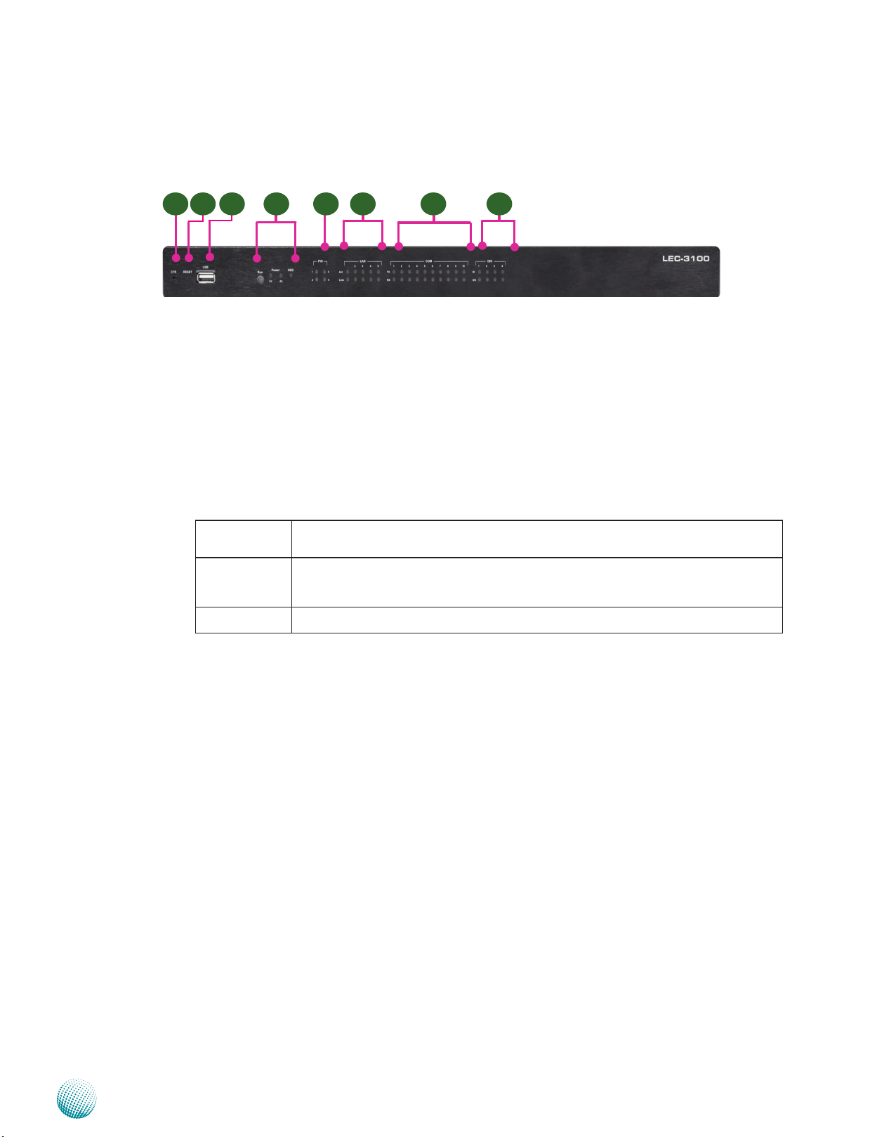
Front Panel Features
F1 F5F2 F3 F4 F6 F7 F8
F1 CTR
This is a software reset switch which could be programmed to reset your application to its default settings.
F2 Reset Switch
It is a hardware reset switch. Use a pointed object to press it 5 seconds then release it to reset the system without
turning off the power.
F3 USB 2.0 type A ports
Introduction
It connects to any USB devices, for example, a flash drive.
F5 Run/Power/HDD LED
Run A programmable dual green/amber LED which can be used for indicating system
status.
Power Green indicates Power-on, where as Off indicates Power-off status.
P1: Status for the built-in power supply unit.
P2: Status for the redundant 1x2-pin Phoenix Contact
Hard Disk Yellow indicates that HDD is present, whereas Off indicates HDD is not present.
F5 PIO Status LED
The set of 4 LEDs can be programmed to display the status of any hardware components or system operating
status. Refer to the Driver and Manual CD for a sample code to implement this feature.
F6 LAN Status LED
ACT LED: If the LED is on, it indicates that the port is linked.
Link LED: If it blinks, it indicates there is traffic.
F7 Serial Port Status LED for COM1 through COM10
The LEDs on the upper row show the status of transmission activities, whereas those on the bottom row show
the status of receiving activities.
F8 These LEDs indicate the Digital I/O operating status.
The LEDs on the upper row show the connection status of input pins, whereas those on the bottom row show
the connection status of output pins.
Embedded and Industrial Computing
3
Page 6

Chapter 1
Rear Panel Features
R1
R2
R4
5 4 3 2 1
Pin 1
COM8
Pin 1
COM7
R5
Pin 1
COM4
Pin 1
COM3
COM2
COM1
Introduction
LAN 2
LAN 4
R3
10 9 8 7 6
Pin 1
COM9COM10
Pin 1
COM6
Pin 1
COM5
Pin 1
R6
R7 R8
LAN 1
LAN 3LAN 5
R9
R1 Power Switch
The power switch comes with the switch which can be used to turn on/off the power from the power
supply.
R2 Power Socket
The AC inlet comes from the unit’s built-in 150W open frame power.
R3 Redundant Power Supply Socket
A redundant power supply through 1x2-pin Phoenix Contact with 9~36V is provided on the system. The
socket also features reversed wiring protection. Hence, it will not cause any damage to the system by reversed
wiring of ground line and power line.
Pin No. 1 2
12
Function DC + DC-
R4 Digital Input/Output port:
The general-purpose input/output (GPIO) peripheral is provided through 10-pin terminal block connector.
Pin 1to 4- Digital Inputs. Pin 6-9-Digital Output.
Pin NO. Pin 1 Pin 2 Pin 3 Pin 4 Pin 5
Assignment
Assignment
R5 20-pin Phoenix Contact Terminal Block
This terminal block can be connected as 8 Com ports with serial port type of RS-232, RS-422 or RS-485; it
supports dip switch selection among RS-232, RS-422 and 485. The following table lists the pin assignments.
Refer to Chapter 3 Motherboard Information for dip switch adjustment information. Note that Pin 1 starts
from right. These connectors are isolated COM ports which will protect system from being damaged due to
power surge or failure of the connected devices.
Port Type
RS-232 SOUT RTS SIN CTS Ground
RS-422 TX+ TX- RX- RX+ Ground
RS-485 TX+ TX- RX- RX+ Ground
RS-485 (2 wires) D+ D- Ground
Embedded and Industrial Computing
Input 0 Input 1 Input 2 Input 3 Ground
Pin NO. Pin 6 Pin 7 Pin 8 Pin 9 Pin 10
Output 0 Output 1 Output 2 Output 3 Ground
Pin NO.
Pin 1 Pin 2 Pin 3 Pin 4 Pin 5
(GND)
(GND)
(GND)
4
Page 7

Chapter 1
R6 Two RS-232 Serial Port (Right: COM1, Left: COM2)
These two serial ports have default operation mode of RS-232 communication channel, but can be configured
as either RS-422 or RS-485 serial communication channel through jumper selection. Refer to Chapter 3
Motherboard Information for jumper selection information. They are also isolated ports.
Pin No. Pin name for RS-232 Pin name for RS-485/RS-422 Pin name for RS-485(2 wires)
1 Data Carrier Detect (DCDA#) TX- D2 Received Data (RXDA) TX+ D+
3 Transmitted Data (TXDA) RX+
4 Data Terminal Ready (DTRA#) RX5 Signal Ground (GND) Ground (GND) Ground (GND)
Introduction
1 2 3 4 5
6 7 8 9
Pin No. Pin name for RS-232 Pin name for RS-485
6 Data Set Ready (DSRA#)
7 Request to Send (RTSA#)
8 Clear to Send (CTSA#)
9 Ring Indicator (RIA#)
R7 DVI-I Connector
It is a Dual Link DVI-I Connector which supports both digital and analog signals, allowing either type of monitor
(analog or digital) to be operated from the same connector (or with a special purpose DVI-A or DVI-I to VGA
cable). By using suitable DVI-I cable, you can connect an appropriate device; for example, an LCD panel.
R8 Two USB 2.0 type A ports
It connects to any USB devices, for example, a flash drive. There is another external port on the front panel and
one internal USB pitch connector on the mainboard.
R9 One FastEthernet LAN port (LAN 5) and 4 Gigabit Ethernet LAN ports (LAN1-4)
LAN 5 is provided by Intel 82562GZ Ethernet controller which supports10/100Mbps connection speeds.
LAN 1-4 are provided by Intel 82574L Ethernet controller which supports10/100/1000Mbps connection
speeds.
Using suitable RJ-45 cable, you can connect LEC-3100 System to a computer, or to any other piece of equipment
that has an Ethernet connection such as a hub or a switch.
Embedded and Industrial Computing
5
Page 8

Chapter 2
Introduction
Chapter 2: Hardware Setup
Preparing the Hardware Installation
To access some components and perform certain service
procedures, you must perform the following procedures
first.
WARNING: To reduce the risk of personal injury,
electric shock, or damage to the equipment,
remove the power cord to remove power from the
server. The front panel Power On/Standby button
does not completely shut off system power.
Portions of the power supply and some internal
circuitry remain active until AC power is removed.
Unpower the LEC-3100 and remove the power cord.1.
Unscrew the 4 threaded screws from the side and 2.
3 from the back of the top cover on the LEC-3100
System.
Slide the cover backwards and open the cover 3.
upwards.
1
Note:
The SO-DIMM installed must meet the speed 1.
requirement (DDR2 533). Do not install DIMMs
supporting different speeds.
The motherboards can support up to 2 GB 2.
memory capacity in maximum.
Installing the Hard Disk
The system can accommodate one Serial-ATA disks. Follow
these steps to install a hard disk into the LEC-3100:
Unsrew the 4 screws on the hard disk tray to take out 1.
the hard disk tray from the system.
Place hard disk on the hard disk tray and align the holes 2.
of the hard disk with the mounting holes on the tray.
Secure the hard disk with 4 mounting screws on the 3.
hard disk tray.
Connect the Serial-ATA power and drive cables to the 4.
hard disk’s power and drive connectors respectively.
Plug the Serial-ATA cables to the Serial-ATA Connectors 5.
on the main board.
Put the hard disk tray with the installed hard disk 6.
back to the system and secure it with the mounting
screws..
Installing the System Memory
The motherboard supports DDR2 memory that features
data transfer rates of 533 MHz to meet the higher
bandwidth requirements of the latest operating system
and Internet applications. It comes with one Double Data
Rate(DDR2) Small Outline Dual Inline Memory Modules
(SO-DIMM) socket.
Align the cutout of the SO-DIMM with the notch of the 1.
memory slot.
Install the SO-DIMM.2.
Notch
Cutout
1
2
Embedded and Industrial Computing
6
Page 9

Chapter 2
Installing a CompactFlash Card
LEC-3100 provides one CompactFlash slot. Follow the
procedures bellow for installing a CompactFlash card.
Align CompactFlash card and the card slot with the 1.
arrow pointing toward the connector.
Push the card to insert into the connector.2.
Introduction
1
2
Embedded and Industrial Computing
7
Page 10

Chapter 3
Chapter 3: Motherboard Information
Block Diagram
The block diagram depicts the relationships among the
interfaces or modules on the motherboard. Please refer
to the following figure for your motherboard’s layout
design.
Motherboard Information
Embedded and Industrial Computing
8
Page 11

Chapter 3
Motherboard Layout
The motherboard layout shows the connectors and
jumpers on the board. Refer to the following picture
as a reference of the pin assignments and the internal
connectors.
Motherboard Information
J2
PS1
LCM1
J5
CN4
PSW1
J11
J1
J8
J13
J6
CON1
J7
SW1/SW2
CN1
J3
CN9
CN8
C10_SW1
C10_SW2
Embedded and Industrial Computing
C7_SW1
C7_SW2
C8_SW1
C8_SW2
C4_SW1
C4_SW2
C6_SW1
C6_SW2
C5_SW1
C5_SW2
SC3T2/SC2T2/SC4T2/
SC3T1/SC2T1/SC4T1/
SC1T2
COM2/COM1
SC1T1
USB2
LAN1
RJ2/RJ1
9
Page 12

Chapter 3
Motherboard Information
Jumper Settings
SATA Connector (J2): The system supports one SATA 2.5”
drive.
The Intel ICH7 provides hardware support for Advanced
Host Controller Interface (AHCI) which is a programming
interface for SATA host controllers. AHCI provides advanced
performance and usability enhancements with SATA such
as Hot-Plug and NCQ (Native Command Queing)
Pin No. Function
7
6
5
4
3
2
1
Note: To configure your Hard disk using the
AHCI feature, you need to enable the AHCI
option in the hard disk configuration of the BIOS
menu.
SATA Power Connector (CON1): Connect the 4-pin SATA
power connector to this port.
1 GND
2 TX+
3 TX4 GND
5 RX6 RX+
7 GND
Pin No. Function
4
3
2
1
1 NC
2 GND
3 GND
4 +5V
Keyboard and mouse interface Connectors(J3): It is
for connecting the PS/2 keyboard and mouse interface
cable.
Function Pin No.
5V 1
MSDATA 3
KBDATA 5
GND 7
2468
1357
Pin No. Function
2 MSCLK
6 KEY
6 KEY
8 KBCLK
Clear CMOS jumper (J1): It is for clearing the CMOS
memory and system setup parameters by erasing the data
stored in the CMOS RAM such as the system passwords.
1
2
3
Pin No. Function
1-2 Normal (Default)
2-3 Clear CMOS
CompactFlash Connector (CN4): It is for connecting a
Compact Flash card to be served as your system’s storage.
The connector is a CF Type II slot which could fit both CF
Type I or CF Type II cards.
CompactFlash Primary/Slave Selection Jumper (J5):
The system’s CompactFlash connects to LEC-3100’s
Primary IDE port in parallel with IDE connector J13. This
jumper configures the CF socket to be the Master (default)
or Slave IDE device.
3
2
1
Pin No. Function
2-3 Master (Default)
1-2 Slave
Digital I/O Connector (CN8): This connector provides 4
digital inputs and 4 digital outputs. The connector type
of LEC-3100 is a plug-in screw terminal block that enables
you to connect to field I/O devices directly.
5 4 3 2 1
10 9 8 7 6
Pin No. 1 2 3 4 5
Function Input 0 Input 1 Input 2 Input 3 Ground
Pn No. 6 7 8 9 10
Function Output 0 Output 1 Output 2 Output 3 Ground
Digital Inputs/Output Requirements
Logic 0: 0 ~ 2V DC
Logic 1: 2 ~ 5V DC
Current limit: Maximum 100mA for each pin
Embedded and Industrial Computing
SO-DIMM Socket (CN1): The 200-pin DDR2 SO-DIMM is
for connecting the DDR2 533 MHz memory. The system
can support up to 2GB in maximum.
Mainboard DC Power Input Connector (PS1): Attach the
4-wires DC power cable to the power input terminal block
on the mainboard. The system has an ATX-style power
input (VDC 24V) and system control.
Pin No. Function
1 DC+ (+24V)
2 DC+ (+24V)
1 2 3 4
3 DC-(GND)
4 DC-(GND)
Phoenix Power Contact (CN9): It is a power socket for
power supply (9~36 VDC) through Phoenix Contact. The
connector provides protection for reversed wiring of
ground line and power line.
Pin No. 1 2
12
Function DC +/- DC -/+
10
Page 13

Chapter 3
Motherboard Information
COM port type adjustment switches (C3_SW1 /C3_SW2,
C4_SW1/C4_SW2, C5_SW1/C5_SW2, C6_SW1/C6_SW2,
C7_SW1/C7_SW2, C8_SW1/C8_SW2, C9_SW1/C9_SW2,
and C10_SW1/C10_SW2): These pairs of switches —
C3_SW1 /C3_SW2, C4_SW1/C4_SW2, C5_SW1/C5_SW2,
C6_SW1/C6_SW2, C7_SW1/C7_SW2, C8_SW1/C8_SW2,
C9_SW1/C9_SW2, and C10_SW1/C10_SW2— are used to
adjust the serial port type for COM3, COM4, COM5, and
COM6, COM7, COM8, COM9, and COM10 respectively. Use
the table below as the switch adjustment information for
COM3 through COM10.
OFF
ON
4
3
2
1
Switch No.
Port Type
RS-232 1 OFF
RS-422
RS-485 (4 Wires)
RS-485 (2 Wires *)
Switch No.
Function
RS-232 1 OFF
RS-422
RS-485 4 Wire
RS-485 2 Wire with /
without Termination
†,‡
(
)
4 ON OFF
Switch 1
2 ON
3 OFF
4 OFF
1 ON
2 OFF
3 OFF
4 OFF
1 ON
2 OFF
3 OFF
4 ON
Switch II
2 OFF
3 OFF
4 OFF
1 ON
2 ON
3 ON
4 OFF
1 ON
2 ON
3 ON
COM1 Serial Type Selection Jumper (SC1T1, SC2T1,
SC3T1, SC4T1): This set of 4 jumpers are used to select
the serial type for COM1 port. Use the table below as the
jumper selection information for COM1.
Jumper
Serial Type
RS-232
(Default)
SCITI SC2T1 SC3T1 SC4T1
1-5
1-2 None None
2-6
3-7
4-8
RS-422 5-9
3-4 2-3 None
6-10
7-11
8-12
RS-485 5-9
5-6 2-3 None
6-10
7-11
8-12
Note: The RS-485 has automatic flow control by
hardware.
COM1 Interface Type and LCM Selection Jumper (J4,
J6): Since the LCM and COM1 interface type shares the
same jumper reference, you also need to adjust Jumpers
J4 and J6 accordingly to select COM1 serial type. Refer to
LCD Module (LCM1) on Page 13 for LCM pinout information.
J4
Jumper
Interface Type
Serial Port (Rs-232
1
2
3
3 2 1
J6
J4 J6
1-2 2-3
/422/485)
LCD Module 2-3 1-2
Note:
COM2 Serial Type Selection Jumper (SC1T2, SC2T2,
* The RS-485 has automatic flow control by
hardware and the default is set by RTS.
† The selector 4 of Switch 2 can only determine
SC3T2, SC4T2): This set of 4 jumpers are used to select
the serial type for COM2 port. Use the table below as the
jumper selection information for COM2.
the termination of RS-485 signal.
‡ The RS-485 2-wire communication has a default
Jumper
SCIT2 SC2T2 SC3T2 SC4T2
setting of termination disabled. The termination
resistor has 120 OHM.
Serial Type
RS-232
(Default)
1-5
2-6
1-2 None None
3-7
4-8
Embedded and Industrial Computing
11
Page 14

Chapter 3
Motherboard Information
Jumper
Serial Type
RS-422 5-9
SCIT2 SC2T2 SC3T2 SC4T2
3-4 2-3 None
6-10
7-11
8-12
RS-485 5-9
5-6 2-3 None
6-10
7-11
8-12
Note: The RS-485 has automatic flow control by
hardware.
COM3~COM 10(CN6 and CN7): The Winbond W83627UHG
Super I/O chipset is connected to the LEC-3100 system
through the LPC bus interfaced to the ICH7M. The Super I/O
chipset provides 6 COM ports- two DB-9 male connectors
and 4 by terminal blocks. The Fintek F81216AD chipset is
also connected to the system through the LPC bus and
provides the addition of 4 COM ports. Together they make
a total of 10 COM ports.
IDE Drive Connector (J13): This 2x22 Pin IDE connector
carries the Primary IDE port signals from the ICH7M chipset.
This port can be used for connection of two drives (Ultra
ATA 33/66/100 IDE Hard Disks with transferring rate of 33
MB/s, 66 MB/s and 88.9 MB/s respectively are supported ).
If two hard disks are connected, one has to be configured
as Master and the other would be Slave, daisy-chained on
a single 44-pin ribbon cable. Since the motherboard’s CF
socket (CN4) also connects in parallel to this set of signals,
the CompactFlash can be configured (via jumper J5) to be
either the Master or Slave IDE device.
Function Pin No.
NC 44
VCC 42
GND 40
HDC CS 1# 38
SA2 36
NC 34
N/C 32
GND 30
GND 28
GND 26
GND 24
GND 22
KEY 20
DATA15 18
DATA14 16
DATA13 14
DATA12 12
DATA11 10
DATA10 8
DATA9 6
DATA8 4
GND 2
44
42
40
38
36
34
32
30
28
26
6
4
2
43
42
41
39
37
35
33
31
29
27
¦
¦
¦
¦
¦
¦
5
3
1
Function Pin No.
GND 43
VCC 41
HDD Active 39
HDC CS0# 37
SA0 35
SA1 33
IRQ 31
DMA ACK# 29
IRDY 27
IOR# 25
IOW# 23
DMA REQ# 21
¦
¦
¦
¦
¦
¦
GND 19
DATA0 17
DATA1 15
DATA2 13
DATA3 11
DATA4 9
DATA5 7
DATA6 5
DATA7 3
RESET# 1
PCI-104 PCI Connector (J11): The mainboard’s PCI-104 PCI
(J11) expansion bus signals are generated by the ICH-7M,
and are essentially identical in function and signaling to a
normal PC motherboard’s PCI bus except for the physical
connector, which is arranged as four 30-pin rows.
Note:
We recommend that you use only Lanner
I/O module with this connector to avoid
incompatibility as some pins have been altered.
A30
D30
Row NO.
Row A Row B Row C Row D
A1
D1
Pin NO.
1 KEY2 NC VCC5 AD0
2 GPIO6 AD2 AD1 VCC5
3 AD5 GND AD4 AD3
4 C/BE-0 AD7 GND AD6
5 GND AD9 AD8 GND
6 AD11 GPIO8 AD10 M66EN_
Pull Low
7 AD14 AD13 GND AD12
8 VCC3 C/BE-1 AD15 VCC3
9 SERR- GND SMB_DAT PAR
10 GND PERR- VCC3 SMB_CLK
11 STOP- VCC3 LOCK- GND
12 VCC3 TRDY- GND DEVSEL13 FRAME- GND IRDY- VCC3
14 GND AD16 VCC3 C/BE-2
15 AD18 VCC3 AD17 GND
16 AD21 AD20 GND AD19
17 VCC3 AD23 AD22 VCC3
18 IDSL0_
AD18
GND IDSL1_
AD19
IDSL2_
AD20
19 AD24 C/BE-3 GPIO9 NC
20 GND AD26 AD25 GND
21 AD29 VCC5 AD28 AD27
22 VCC5 AD30 GND AD31
23 REQ-0 GND REQ-1 GPIO12
24 GND REQ-2 VCC5 GNT-0
25 GNT-1 GPIO7 GNT-2 GND
26 VCC5 PCICLK0 GND PCICLK1
27 PCICLK2 VCC5 PCICLK3 GND
28 GND PIRQ-D VCC5 PCIRST29 NC PIRQ-A PIRQ-B PIRQ-C
30 PCI_PME# REQ-3 GNT-3 KEY1
Embedded and Industrial Computing
12
Page 15

Chapter 3
Motherboard Information
USB 2.0 Ports (J8): The board provides 4 USB 2.0 type A
ports. Dual ports on the front panel (Reference NO.: J7),
one port on the back panel (Reference No.: USB2), and
one USB pitch (Reference No.: J8) on the board.
USB3
4
3
2
1
Pin No. Function
1 USB_VCC
2 USB-
3 USB+
4 GND
LCD Module (LCM1): The LCD module connector is a
serial type port which can be connected to display the
real-time operating status and conguration parameters
of the system.
Ground Data
Terminal
Ready
(DTR1 #)
9 7 5 3 1 Pin No.
Transmit Data
(TXD1)
9 7 5 3 1
Receive
Data (RXD1)
Data
Carrier
Detect
(DCD1#)
Function
Software Reset Switch by GPIO (SW2): In addition to
the hardware reset switch (SW1), the software reset by
GPIO can be programmed to suit your specic application need. For example, it could reset a software to its
default settings. Refer to the description of CTR on Front
Panel Features in Chapter 1, Introduction. Look in your
Driver and Manual CD for sample code to implement this
feature.
Pin No. Function
1 GPIO 12 signal
2 Ground
3 Ground
4 Ground
Hardware Reset Switch(SW1): Compared to SW2, this
is a hardware reset switch which can be used to reset the
system without turning o the power.
Pin No. Function
1 Reset Signal
2 Ground
3 Ground
4 Ground
DVI-I Connector (DVII1):
10 8 6 4 2
10. 8 6 4 2 Pin No.
KEY Ring Indicator
(RI1#)
Clear to Send
(CTS1#)
Request
to Send
(RTS1#)
Data Set
Ready
(DSR1#)
Function
Note: In order to connect the LCM, you will need
to adjust BOTH Jumper J4 and J6 accordingly.
Note that COM1 will be disabled when the jumper
setting is set to LCD Module use. Refer to the COM1
Interface Type and LCM Selection Jumper (J4, J6) on
the previous page for more information.
Jumper
Interface Type
Serial Port (Rs-232
J4 J6
1-2 2-3
/422/485)
LCD Module 2-3 1-2
Pin No. Function Pin No. Function
1 TMDS Data 2¬ 13 TMDS Data 3+
2 TMDS Data 2+ 14 5V
3 TMDS Data 2/4 shield 15 GND
4 TMDS Data 4¬ 16 HOT PLUG DET
5 TMDS Data 4+ 17
6 DDC CLOCK 18
7 DDC DATA 19 TMDS Data 0/5 shield
8 Analog vertical sync 20 TMDS Data 5¬
9 TMDS Data 1¬ 21 TMDS Data 5+
10 TMDS Data 1+ 22
11 TMDS Data 1/3 shield 23
12 TMDS Data 3¬ 24
C1 Analog Red
C2 Analog Green
C5 Analog GND
C3 Analog Blue
C4 Analog Horizontal sync
TMDS Data 0
TMDS Data 0+
TMDS CLK shield
TMDS CLK+
TMDS CLK¬
ATX Power Button Connector (PSW1)
Embedded and Industrial Computing
1 2
Pin No. Function
1 PANSW2 GND
13
Page 16

Appendix
Terms and Conditions
Appendix: Terms and Conditions
Warranty Policy
All products are under warranty against defects in 1.
materials and workmanship for a period of one year
from the date of purchase.
The buyer will bear the return freight charges for 2.
goods returned for repair within the warranty period;
whereas the manufacturer will bear the after service
freight charges for goods returned to the user.
The buyer will pay for repair (for replaced components 3.
plus service time) and transportation charges (both
ways) for items after the expiration of the warranty
period.
If the RMA Service Request Form does not meet the 4.
stated requirement as listed on “RMA Service,” RMA
goods will be returned at customer’s expense.
The following conditions are excluded from this 5.
warranty:
RMA Service
Requesting a RMA#
To obtain a RMA number, simply fill out and fax the 6.
“RMA Request Form” to your supplier.
The customer is required to fill out the problem code 7.
as listed. If your problem is not among the codes listed,
please write the symptom description in the remarks
box.
Ship the defective unit(s) on freight prepaid terms. 8.
Use the original packing materials when possible.
Mark the RMA# clearly on the box. 9.
Note: Customer is responsible for shipping
damage(s) resulting from inadequate/loose
packing of the defective unit(s). All RMA# are valid
for 30 days only; RMA goods received after the
effective RMA# period will be rejected.
Improper or inadequate maintenance by the customer
Unauthorized modification, misuse, or reversed
engineering of the product Operation outside of the
environmental specifications for the product.
Embedded and Industrial Computing
14
Page 17

Appendix
RMA Service Request Form
When requesting RMA service, please fill out the following form. Without
this form enclosed, your RMA cannot be processed.
RMA No:
Reasons to Return: Ŀ Repair(Please include failure details)
Ŀ Testing Purpose
Company: Contact Person:
Phone No. Purchased Date:
Fax No.: Applied Date:
Return Shipping Address:
Shipping by: Ŀ Air Freight Ŀ Sea Ŀ Express ___
Ŀ Others:________________
Item Model Name Serial Number Configuration
Item Problem Code Failure Status
*Problem Code:
01:D.O.A.
02: Second Time
R.M.A.
03: CMOS Data Lost
04: FDC Fail
05: HDC Fail
06: Bad Slot
07: BIOS Problem
08: Keyboard Controller Fail
09: Cache RMA Problem
10: Memory Socket Bad
11: Hang Up Software
12: Out Look Damage
13: SCSI
14: LPT Port
15: PS2
16: LAN
17: COM Port
18: Watchdog Timer
19: DIO
20: Buzzer
21: Shut Down
22: Panel Fail
23: CRT Fail
24: Others (Pls specify)
Request Party
Confirmed By Supplier
Authorized Signature / Date Authorized Signature / Date
Terms and Conditions
Embedded and Industrial Computing
15
 Loading...