

Page 1

ÑmSQMM=
pbosf`b=j^kr^i=
=
sЙклбзе=O
i~ДKЦкмййЙе=^_=
dмддкЙЦело®ЦЙе=NSI=pbJQPQ=QQ==hrkdp_^`h^I=ptbabk=
mЬзеЙW=HQS=PMM=RS=OU=MM=
c~сW=HQS=PMM=RS=OU=VV=
беСз]д~ДЦкмййЙеKЕзг
пппKд~ДЦкмййЙеKЕзг=
=
Page 2

=
= pЙкобЕЙ=j~ем~д=СmSQMM= m~ÖÉ=N=EUF=
fP6400
Functional description for class TD amplifiers.................................................3
Functional description schematics ....................................................................5
Internal connections ..........................................................................................6
Component list..................................................................................................7
Variant specific components.............................................................................7
Description for variant dependent components.................................................7
Sparepart list for fP6400 ...................................................................................8
A20TDH
Schematics for A20TDH...................................................................................2
Board placement for A20TDH..........................................................................3
Component list for A20TDH-32-2 - rev 02.......................................................4
A20TDL
Schematics for A20TDL ...................................................................................2
Board placement for A20TDL ..........................................................................3
Component list for A20TDL - rev 02A.............................................................4
Variant specific components.............................................................................7
Description for variant dependent components.................................................8
IN2GTD
Schematics for IN2GTD ...................................................................................2
Board placement for IN2GTD ..........................................................................3
Component list for IN2GTD - rev 02A.............................................................4
Variant specific components.............................................................................7
Description for variant dependent components.................................................8
LD92
Schematics for LD92 ........................................................................................2
Board placement for LD92................................................................................3
Component list for LD92 - rev 01.....................................................................4
Variant specific components.............................................................................5
Description for variant dependent components.................................................6
SP80CB
Schematics for SP80CB....................................................................................2
Board placement for SP80CB ...........................................................................3
Component list for SP80CB-2x32-2 - rev 01A.................................................4
SP80FA / SP80FB
Functional description for switch mode powersupply SP80FA & SP80FB......2
Schematics for SP80FA & SP80FB..................................................................4
Schematics for SP80FA, SP80FB & PIND.......................................................5
SP80FA.............................................................................................................6
Board placement for SP80FA - rev 04..............................................................6
Board placement for SP80FA - rev 06..............................................................7
Component list for SP80FA - rev 06.................................................................8
Variant specific components for 230V versions - rev 06..................................9
Page 3

=
= pЙкобЕЙ=j~ем~д=СmSQMM= m~ÖÉ=O=EUF=
Variant specific components for 115V versions - rev 06................................10
Description for variant dependent components...............................................11
SP80FB ...........................................................................................................12
Board placement for SP80FB & PIND ...........................................................12
Component list for PIND, SP80FB - rev 01A.................................................13
Variant specific components for 230V versions - rev 01A .............................15
Variant specific components for 115V versions - rev 01A .............................16
Description for variant dependent components...............................................17
Page 4

=
= pЙкобЕЙ=j~ем~д=СmSQMM= m~ÖÉ=P=EUF=
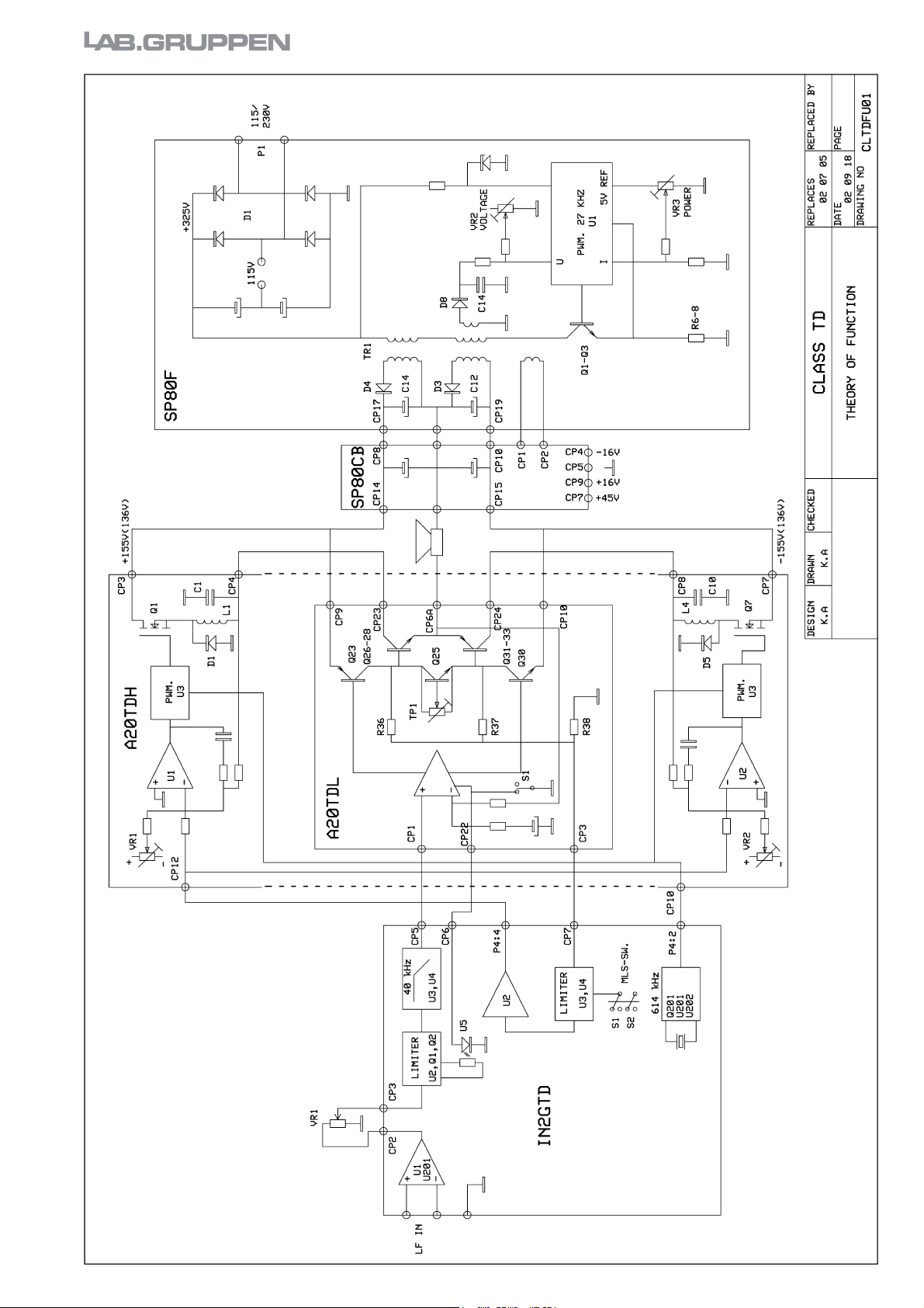
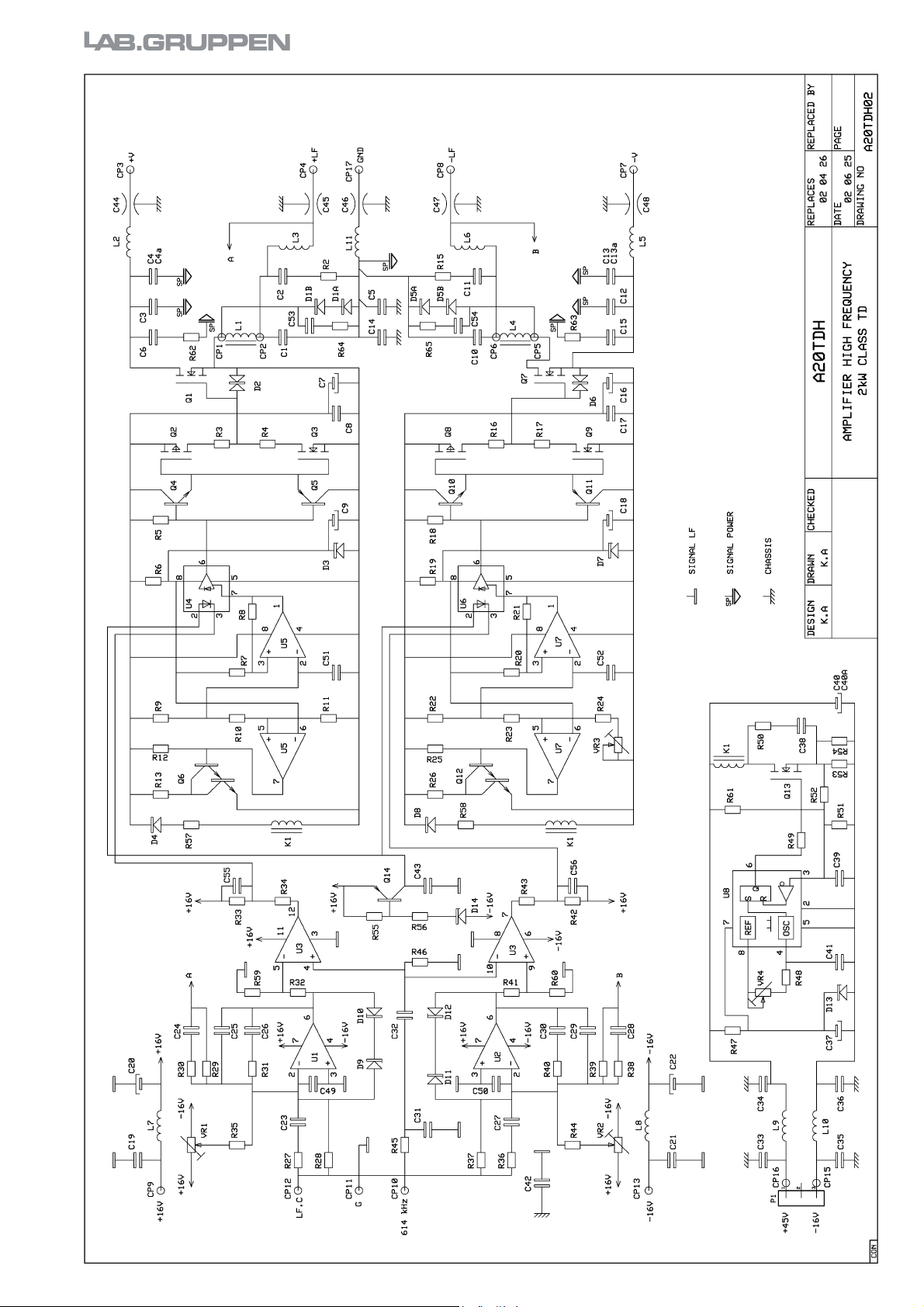
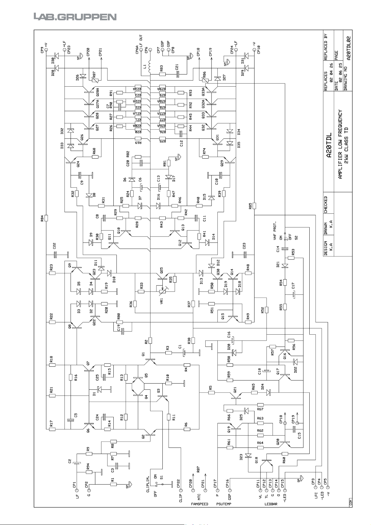
cмеЕнбзе~д=ЗЙлЕкбйнбзе=Сзк=Ед~лл=qa=~гйдбСбЙкл=
Theory of function
The input signal is connected to the balanced amplifier and gain switch U1, U201 on the IN2GTD-board. The signal is then
passing the gain control on the front panel, going to amplifier U2 (IN2GTD). The gain in this amplifier can be reduced by opto
resistor U5 to prevent clipping in the output amplifier. Limiter Q1, Q2 together with the phase linear lowpassfilter U3, U4 limits
the slewrate of the signal going to the output amplifier A20TDL, preventing intermodulation in this amplifier if signals of too
high frequencies are presented on the input terminal.
The output amplifier A20TDL works as an ordinary power amplifier with the difference that the collector voltage to the output
transistors is supplied from the switch mode amplifier A20TDH. The base voltage of the output transistors Q26-Q28, Q31-Q33
(A20TDL) is sensed by voltage divider R36-R38 and is then sent to the adjustable limiter U3, U4 on the IN2GTD-board, before
it reaches the input of the switch mode amplifier (A20TDH) . Limit level is set by the MLS switches S1 and S2. This limiter is
used to limit the maximum output voltage from the amplifier. These switches also change the sensitivity for the led bars on the
front panel.
The amplifier U1 (U2) on the A20TDH-board makes sure that the output signal on terminal CP4 (CP8) is a copy of the input
signal on terminal CP12, by giving correct control voltage to pulse width modulator U3. U3 compares this voltage with an
614kHz triangular wave giving a pulse width modulated output signal from Q1 (Q7) which is filtered by L1, C1 (L4, C10). The
gain from the base of the output transistors on the A20TDL-board to the output of the A20TDH-board is equal to one. VR1
(VR2) is used to add a DC-offset on the input of U1 (U2) giving +7,5V (CP4) -7,5V (CP8) relative output of the LF-amplifier
(CP6A), which is the same as collector-emitter voltage for the output transistors Q26-Q28 and Q31-Q33.
Repairing instructions
REQUIRED MEASUREMENT EQUIPMENT:
-Audio generator
-Dummy load, 16 ohm
-AC-voltmeter/THD-meter
-2 digital voltmeters
-Two channel oscilloscope for audio
1. Without changing any fuses check the power supply +155V, -155V, +16V, -16V and +45V. If these aren't OK go to the
service manual for the power supply. (The +45V voltage is not regulated and can vary between 30 and 60V depending on
the load of the power supply.)
2. If all fuses are OK, follow the signal from input to output, and repair in normal way. The best way is to place the
amplifier on the front handles, loosen the rear panel, and mount it back on distances (delivered with this manual) to make
it possible to measure.
3. If there is a fault in the power amplifier stage do as follows:
3:1 Turn VR1, VR2 (A20TDH) and VR3 (SP80FB) counter clockwise.
3:2 Short-circuit R38 on A20TDL-board.
3:3 Disconnect cables from CP23 and CP24 (A20TDL) (Q26-Q28 and Q31-Q33 collectors).
3:4 Replace broken fuses. (only for the channel you repair)
3:5 Connect DC-voltmeter (200V) to the positive (negative) rail voltage.
3:6 Connect another DC-voltmeter (20V) to the cable disconnected from CP23 (CP24).
3:7 Turn VR3 (SP80FB) slowly clockwise, and watch the voltmeters. Rail voltage should increase rapidly, "collector
voltage" should read 0. After turning VR3 maximum 30
°, rail voltage should be 155V.
Page 5

=
= pЙкобЕЙ=j~ем~д=СmSQMM= m~ÖÉ=Q=EUF=
a) If the rail voltage is zero or very low, check Q1, D1A, D1B (Q7, D5A, D5B) (shorted) on the A20TDH-
board. If Q1 (Q7) is broken, also replace R3 (R16) and D2 (D6).
b) If the rail voltage is OK, turn VR1 (VR2) on the A20TDH-board slowly maximum clockwise. Voltage
measured on the disconnected collector cable should stop at about 7,5V.
c) If OK turn VR1 (VR2) (A20TDH) and TP3 (SP80FB) counter clockwise.
3:8 Repeat from 3:5 for the negative side.
3:9 Reconnect cable to CP23 (Q26-Q28 collector).
3:10 Connect dummy load 16 ohm to output, and connect an oscilloscope (10V/div) across the load.
3:11 Slowly turn VR3 (SP80FB) for 155V (-155V) rail voltage.
3:12 Slowly turn VR1 (VR2) (A20TDH) clockwise and look at the oscilloscope. There should be no DC on the
oscilloscope. If there is DC (>1V) repair the positive (negative) output section on the A20TDL-board.
3:13 Turn back VR1 (VR2) (A20TDH) and VR3 (SP80FB), and disconnect the cable from CP23 (Q26-Q28 collector).
3:14 Reconnect cable to CP24 (Q31-Q33 collector) and repeat from 3:11 for the negative side.
3:15 Reconnect cables to CP23 and CP24. Turn VR3 for 155V rail voltage. Turn VR1 clockwise, no DC on the
oscilloscope. Then slowly turn VR2 clockwise. There can be some oscillation with VR2 in middle position, but it
will stop at further turning.
3:16 Connect 1kHz sine wave to the input of the amplifier. Adjust gain until there is signal on the output. It should be a
7V PK sine wave with no distortion.
3:17 Disconnect short circuit from R38, and the amplifier will work.
Page 6
=
= pЙкобЕЙ=j~ем~д=СmSQMM= m~ÖÉ=R=EUF=
cмеЕнбзе~д=ЗЙлЕкбйнбзе=лЕЬЙг~нбЕл=
Page 7
=
= pЙкобЕЙ=j~ем~д=СmSQMM= m~ÖÉ=S=EUF=
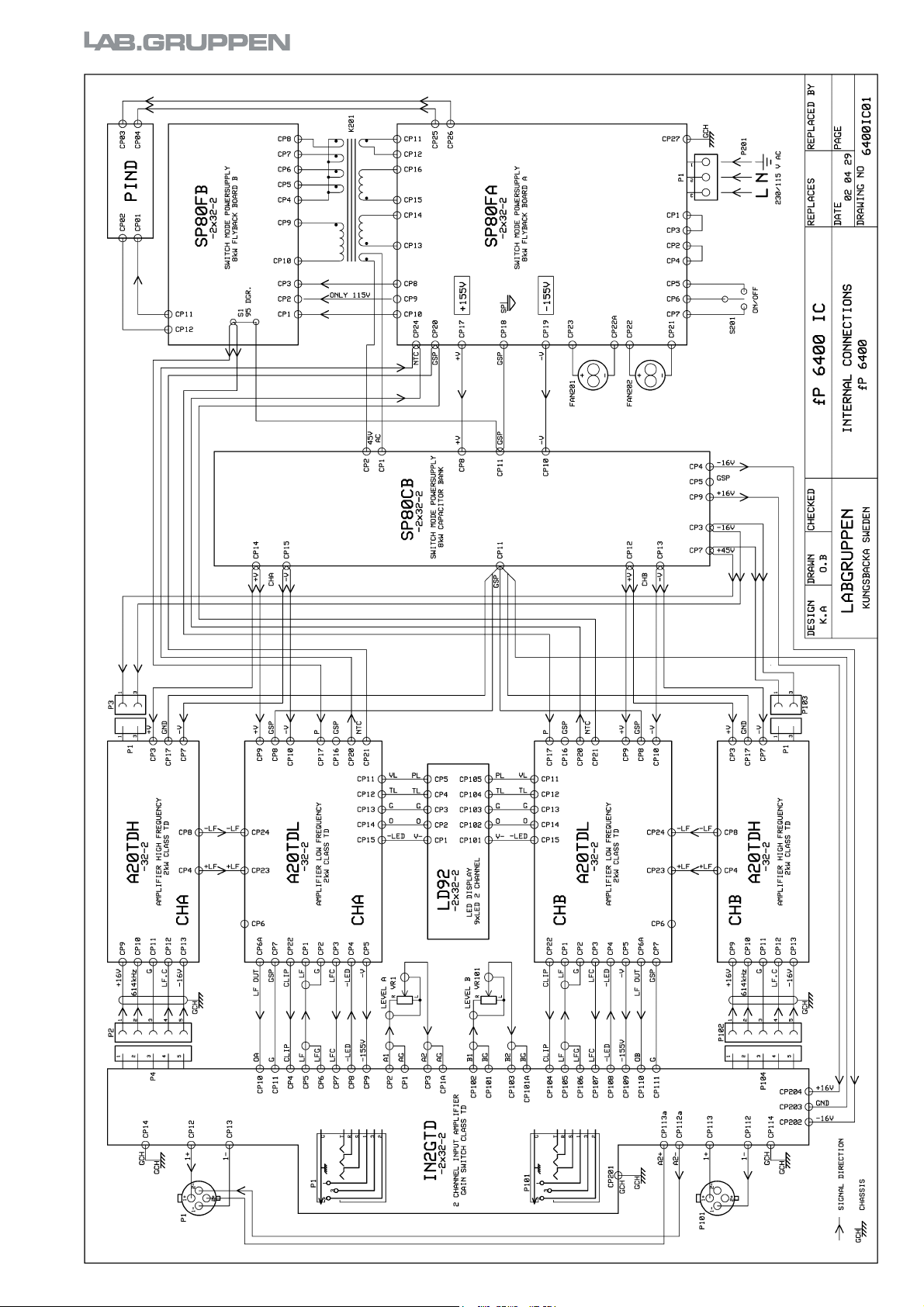
fенЙке~д=ЕзееЙЕнбзел=
Page 8
=
= pЙкобЕЙ=j~ем~д=СmSQMM= m~ÖÉ=T=EUF=
`згйзеЙен=дблн=
- Safety critical component. Should only be replaced with the specified type.
Position Partnumber Description Comment
FAN201 F80x25-24HS Fan 80x80x25mm 24VDC high speed
FAN202 F80x25-24HS Fan 80x80x25mm 24VDC high speed
K201 6K4FUI9330_LAB Trafo. 6,4KW flyback U93/76/30 I93/28/30 core LAB. Rev01
P1 NL4MP_NEU Connector speakon 4pole NEUTRIK NL4MP
P2 CASOC5P270_LAB Cable assembly socket crimp terminal 5pole L270mm LAB. Rev01
P3 SOIDC3P1M_AMP Socket IDC terminal 3pole 1module AMP 640441-3
P101 NL4MP_NEU Connector speakon 4pole NEUTRIK NL4MP
P102 CASOC5P270_LAB Cable assembly socket crimp terminal 5pole L270mm LAB. Rev01
P103 SOIDC3P1M_AMP Socket IDC terminal 3pole 1module AMP 640441-3
P201 Variant dependent, see separate list
P201A Variant dependent, see separate list
S201 Variant dependent, see separate list
VR1 VR10KLIN31_TOK Potentiometer 10K LIN 31step TOKOS B103 TP96N08 Y4929 Rev1
VR101 VR10KLIN31_TOK Potentiometer 10K LIN 31step TOKOS B103 TP96N08 Y4929 Rev1
s~кб~ен=лйЙЕбСбЕ=ЕзгйзеЙенл=
Position 230V 115V
P201 MLEU3x1.52.5mBLK SJOOW-3xAWG12
P201A - MP5-15P15A125V
S201 RK1-1-10A15x21 RK1-1-6A15x21
aЙлЕкбйнбзе=Сзк=о~кб~ен=ЗЙйЙеЗЙен=ЕзгйзеЙенл=
Partnumber Description
MLEU3x1.52.5mBLK Mains lead EU Plug type CEE7/VII 3x1.5mm2 2.5m Black
MP5-15P15A125V Mains plug type 5-15P 15A 125V
RK1-1-10A15x21 Switch Rocker Single Pole Double Trough on - on 10A 15x21mm
RK1-1-6A15x21 Switch Rocker Single Pole Double Trough on - on 6A 15x21mm
SJOOW-3xAWG12 Cable SJOOW 3xAWG12 UL style 817
Page 9
=
= pЙкобЕЙ=j~ем~д=СmSQMM= m~ÖÉ=U=EUF=
pé~êÉé~êí=äáëí=Ñçê=ÑmSQMM=
Completed modules
Partnumber Description
A20TDH-32-2 Amplifier high frequency 2kW class TD, variant 32-2
A20TDL-32-2 Amplifier low frequency 2kW class TD, variant 32-2
IN2GTD-2x32-2 2 channel input amplifier and gainswitch class TD, variant 2x32-2
LD92-2x32-2 Led display 9 x led 2 channel, variant 2x32-2
SP80CB-2x32-2 Switch mode powersupply 8kW capacitor bank, variant 2x32-2
SP80FA-2x32-2 Switch mode powersupply 8kW flyback board A, variant 2x32-2, 230V
SP80FA-2x32-2U Switch mode powersupply 8kW flyback board A, variant 2x32-2U, 115V
SP80FB-2x32-2 Switch mode powersupply 8kW flyback board B, variant 2x32-2, 230V
SP80FB-2x32-2U Switch mode powersupply 8kW flyback board B, variant 2x32-2U, 115V
PIND-2x32-2 Led display power indication 2 x led, 230V
PIND-2x32-2U Led display power indication 2 x led, 115V
Mecanical parts
- Safety critical component. Should only be replaced with the specified type.
Partnumber Description
TCA20TDA-PBLK Top / bottom cover
FP-FP6400 Front panel
SPLA20TDA-A Side panel left
SPRA20TDA-A Side panel right
RP-FP6400 Rear panel 230V
RP-FP6400U Rear panel 115V
HDL2HEM5_MEN Handle
DCSL1-PBLK Dustfilter clip left
DCSR1-PBLK Dustfilter clip right
DF139x62x5-20
DF115x62x5-20
KNBD18.5_TAI Gain potentiometer knob
Screws
Partnumber Description
MRX3x10SV Machine screw, pan head, phillips, M3x10, black
MFX3x12SV Machine screw, countersunk head, phillips, M3x12, black
MFX3x20SV Machine screw, countersunk head, phillips, M3x20, black
RTS-HST2.9x9.5SV Self tapping screw, pan head, torx, 2.9x9.5mm, black
MC6S4x10FBB-SV Hexagon socket screw, cap head, M4x10 with spring washer, black
LAB_T3x8-SV Top / bottom cover screw, torx, M3x8, black
Dustfilter left
Dustfilter right
Page 10

=
= pЙкобЕЙ=j~ем~д=^OMqae= m~ÖÉ=N=ETF=
A20TDH
Schematics for A20TDH...................................................................................2
Board placement for A20TDH..........................................................................3
Component list for A20TDH-32-2 - rev 02.......................................................4
Page 11
=
= pЙкобЕЙ=j~ем~д=^OMqae= m~ÖÉ=O=ETF=
pÅÜÉã~íáÅë=Ñçê=^OMqae=
Page 12
=
= pЙкобЕЙ=j~ем~д=^OMqae= m~ÖÉ=P=ETF=
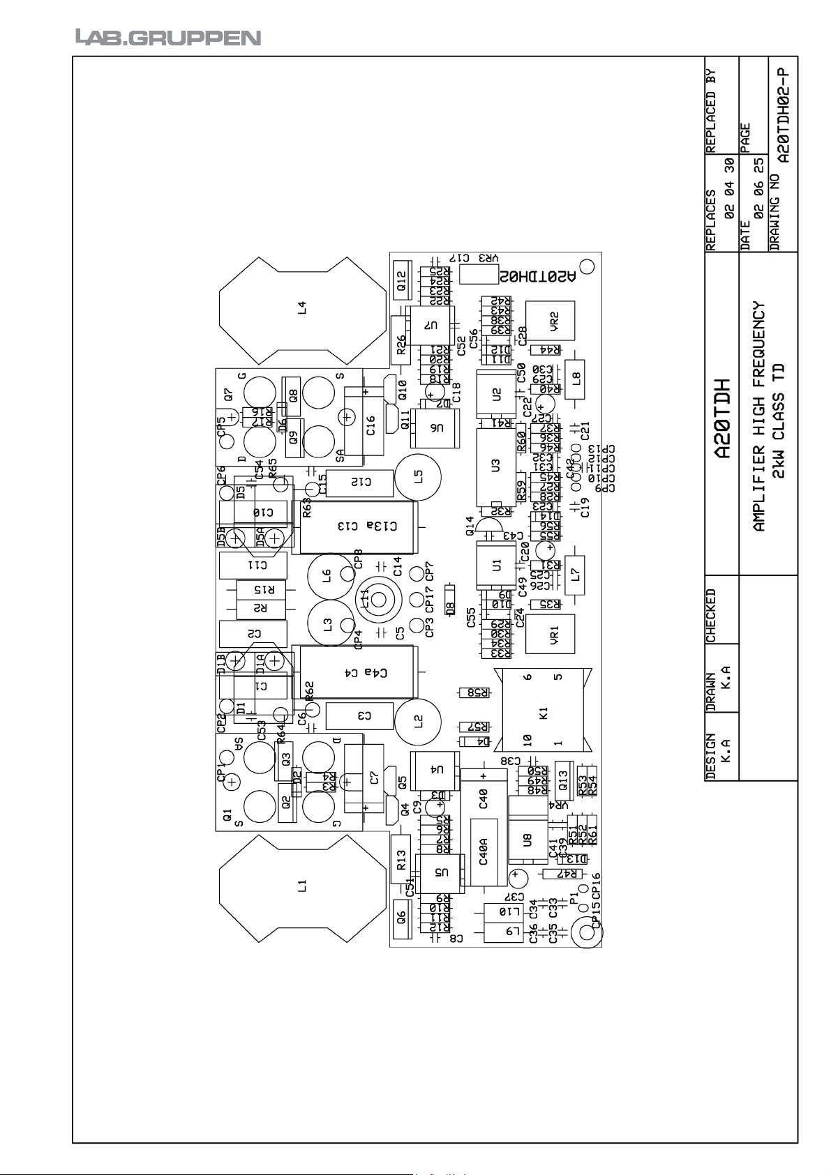
_ç~êЗ=йд~ЕЙгЙен=Сзк=^OMqae=
Page 13
=
= pЙкобЕЙ=j~ем~д=^OMqae= m~ÖÉ=Q=ETF=
`згйзеЙен=дблн=Сзк=^OMqaeJPOJO=J=кЙо=MO=
- Safety critical component. Should only be replaced with the specified type.
Position Partnumber Description Comment Side
C1 330n250VMMK15 Capacitor polyester 330n 250V MMK 15mm Top
C2 330n250VMMK15 Capacitor polyester 330n 250V MMK 15mm Top
C3 330n250VMMK15 Capacitor polyester 330n 250V MMK 15mm Top
C4 3u3160VMKP27.5 Capacitor polypropylene 3u3 160V MKP 27.5mm May have different
C5 1u50VMMK5 Capacitor polyester 1u 50V MMK 5mm Top
C6 4n7200VX7R5%5 Capacitor ceramic 4n7 200V X7R 5% 5mm Top
C7 470u10V10x18A Capacitor electrolytic 470u 10V 10x18mm axial Top
C8 100n63VMMK5 Capacitor polyester 100n 63V MMK 5mm Top
C9 10u50V Capacitor electrolytic 10u 50V 5mm Top
C10 330n250VMMK15 Capacitor polyester 330n 250V MMK 15mm Top
C11 330n250VMMK15 Capacitor polyester 330n 250V MMK 15mm Top
C12 330n250VMMK15 Capacitor polyester 330n 250V MMK 15mm Top
C13 3u3160VMKP27.5 Capacitor polypropylene 3u3 160V MKP 27.5mm May have different
C14 1u50VMMK5 Capacitor polyester 1u 50V MMK 5mm Top
C15 4n7200VX7R5%5 Capacitor ceramic 4n7 200V X7R 5% 5mm Top
C16 470u10V10x18A Capacitor electrolytic 470u 10V 10x18mm axial Top
C17 100n63VMMK5 Capacitor polyester 100n 63V MMK 5mm Top
C18 10u50V Capacitor electrolytic 10u 50V 5mm Top
C19 100n63VMMK5 Capacitor polyester 100n 63V MMK 5mm Top
C20 10u50V Capacitor electrolytic 10u 50V 5mm Top
C21 100n63VMMK5 Capacitor polyester 100n 63V MMK 5mm Top
C22 10u50V Capacitor electrolytic 10u 50V 5mm Top
C23 2n2250VMMK5 Capacitor polyester 2n2 250V MMK 5mm Top
C24 100p200VNP05%5 Capacitor ceramic 100p 200V NP0 5% 5mm Top
C25 39p200VNP05%5 Capacitor ceramic 39p 200V NP0 5% 5mm Top
C26 270p100VNP05%5 Capacitor ceramic 270p 100V NP0 5% 5mm Top
C27 2n2250VMMK5 Capacitor polyester 2n2 250V MMK 5mm Top
C28 100p200VNP05%5 Capacitor ceramic 100p 200V NP0 5% 5mm Top
C29 39p200VNP05%5 Capacitor ceramic 39p 200V NP0 5% 5mm Top
C30 270p100VNP05%5 Capacitor ceramic 270p 100V NP0 5% 5mm Top
C31 68p200VNP05%5 Capacitor ceramic 68p 200V NP0 5% 5mm Top
C32 1n200VNP05%5 Capacitor ceramic 1n 200V NP0 5% 5mm Top
C33 100n63VMMK5 Capacitor polyester 100n 63V MMK 5mm Top
C34 100n63VMMK5 Capacitor polyester 100n 63V MMK 5mm Top
C35 100n63VMMK5 Capacitor polyester 100n 63V MMK 5mm Top
C36 100n63VMMK5 Capacitor polyester 100n 63V MMK 5mm Top
C37 10u50V Capacitor electrolytic 10u 50V 5mm Top
C38 1n200VNP05%5 Capacitor ceramic 1n 200V NP0 5% 5mm Top
C39 220p200VNP05%5 Capacitor ceramic 220p 200V NP0 5% 5mm Top
C40 - Not used Top
C40A 2u2100VMMK15 Capacitor polyester 2u2 100V MMK 15mm Top
C41 1n200VNP05%5 Capacitor ceramic 1n 200V NP0 5% 5mm Top
C42 100n50VY5W5%5 Capacitor ceramic 100n 50V Y5W 5% 5mm Bot.
C43 - Not used Top
C44 1n5200V_MUR Feed trough capacitor 1n5 200V Murata
C45 1n5200V_MUR Feed trough capacitor 1n5 200V Murata
TF418454E152P
TF418454E152P
value
value
Bot.
Bot.
Top
Top
Page 14
=
= pЙкобЕЙ=j~ем~д=^OMqae= m~ÖÉ=R=ETF=
Position Partnumber Description Comment Side
C46 1n5200V_MUR Feed trough capacitor 1n5 200V Murata
TF418454E152P
C47 1n5200V_MUR Feed trough capacitor 1n5 200V Murata
TF418454E152P
C48 1n5200V_MUR Feed trough capacitor 1n5 200V Murata
TF418454E152P
Bot.
Bot.
Bot.
C49 220p200VNP05%5 Capacitor ceramic 220p 200V NP0 5% 5mm Top
C50 220p200VNP05%5 Capacitor ceramic 220p 200V NP0 5% 5mm Top
C51 1n200VNP05%5 Capacitor ceramic 1n 200V NP0 5% 5mm Top
C52 1n200VNP05%5 Capacitor ceramic 1n 200V NP0 5% 5mm Top
C53 470p200VNP05%5 Capacitor ceramic 470p 200V NP0 5% 5mm Top
C54 470p200VNP05%5 Capacitor ceramic 470p 200V NP0 5% 5mm Top
C55 - Not used Top
C56 - Not used Top
D1 - Not used Bot.
D1A BYW81PI200LY Diode power BYW81PI200 lying Bot.
D1B BYW81PI200LY Diode power BYW81PI200 lying Bot.
D2 BZW06P15B Diode transient voltage suppression BZW06P15B Top
D3 5V6.4W2% Diode zener 5V6 .4W 2% Top
D4 BYW100-200 Diode power switch BYW100-200 Top
D5 - Not used Bot.
D5A BYW81PI200LY Diode power BYW81PI200 lying Bot.
D5B BYW81PI200LY Diode power BYW81PI200 lying Bot.
D6 BZW06P15B Diode transient voltage suppression BZW06P15B Top
D7 5V6.4W2% Diode zener 5V6 .4W 2% Top
D8 BYW100-200 Diode power switch BYW100-200 Top
D9 12V.4W5% Diode zener 12V .4W 5% Top
D10 12V.4W5% Diode zener 12V .4W 5% Top
D11 12V.4W5% Diode zener 12V .4W 5% Top
D12 12V.4W5% Diode zener 12V .4W 5% Top
D13 18V1.3W5% Diode zener 18V 1.3W 5% Top
D14 27V.4W5% Diode zener 27V .4W 5% Top
K1 T5WFE20-10-6_LAB Transformer 5W flyback E20-10-6 LHM core
LAB.GRUPPEN Rev 01
Top
L1 13uHRM14_LAB Inductor 13uH RM14 LAB.GRUPPEN Rev 01 Top
L2 u5HD1.18ST_LAB Inductor u5H Lab.gruppen Rev 01 Top
L3 u5HD1.18ST_LAB Inductor u5H Lab.gruppen Rev 01 Top
L4 13uHRM14_LAB Inductor 13uH RM14 LAB.GRUPPEN Rev 01 Top
L5 u5HD1.18ST_LAB Inductor u5H Lab.gruppen Rev 01 Top
L6 u5HD1.18ST_LAB Inductor u5H Lab.gruppen Rev 01 Top
L7 47uHA6M Inductor 47uH axial 6 modules Top
L8 47uHA6M Inductor 47uH axial 6 modules Top
L9 47uHA6M Inductor 47uH axial 6 modules Top
L10 47uHA6M Inductor 47uH axial 6 modules Top
L11 u5HD1.18ST_LAB Inductor u5H Lab.gruppen Rev 01 Top
P1 PH3P90L1M_AMP Pin header 3pole 90dg locking 1module AMP 640457-3 Top
Q1 IXFN73N30 Transistor MOS power IXFN73N30 Bot.
Q2 MTP2955 Transistor MOS power MTP2955 Top
Q3 BUZ71 Transistor MOS power BUZ71 Top
Q4 ZTX651STZ Transistor bipolar signal ZTX651STZ Top
Q5 ZTX751STZ Transistor bipolar signal ZTX751STZ Top
Q6 TIP120 Transistor bipolar power TIP120 Top
Q7 IXFN73N30 Transistor MOS power IXFN73N30 Bot.
Q8 MTP2955 Transistor MOS power MTP2955 Top
Q9 BUZ71 Transistor MOS power BUZ71 Top
Q10 ZTX651STZ Transistor bipolar signal ZTX651STZ Top
Page 15
=
= pЙкобЕЙ=j~ем~д=^OMqae= m~ÖÉ=S=ETF=
Position Partnumber Description Comment Side
Q11 ZTX751STZ Transistor bipolar signal ZTX751STZ Top
Q12 TIP120 Transistor bipolar power TIP120 Top
Q13 IRF730 Transistor MOS power IRF730 Top
Q14 BC557B Transistor bipolar signal BC557B Top
R2 2R22W5%SO5 Resistor metal film 2R2 2W 5% 5mm stand off Top
R3 4R7.25W5% Resistor Carbon Film 4R7.25W5% Top
R4 1R1W5%SO5 Resistor metal film 1R 1W 5% 5mm stand off Top
R5 680R.25W5% Resistor Carbon Film 680R.25W5% Top
R6 47R.25W5% Resistor Carbon Film 47R.25W5% Top
R7 2K2.7W1% Resistor Metal Film 2K2.7W1% Top
R8 22K.25W5% Resistor Carbon Film 22K.25W5% Top
R9 820R.25W5% Resistor Carbon Film 820R.25W5% Top
R10 47R.25W5% Resistor Carbon Film 47R.25W5% Top
R11 2K2.7W1% Resistor Metal Film 2K2.7W1% Top
R12 4K7.7W1% Resistor Metal Film 4K7.7W1% Top
R13 15R6W5%SO5 Resistor wirewound 15R 6W 5% 5mm stand off Top
R15 2R22W5%SO5 Resistor metal film 2R2 2W 5% 5mm stand off Top
R16 4R7.25W5% Resistor Carbon Film 4R7.25W5% Top
R17 1R1W5%SO5 Resistor metal film 1R 1W 5% 5mm stand off Top
R18 680R.25W5% Resistor Carbon Film 680R.25W5% Top
R19 47R.25W5% Resistor Carbon Film 47R.25W5% Top
R20 2K2.7W1% Resistor Metal Film 2K2.7W1% Top
R21 22K.25W5% Resistor Carbon Film 22K.25W5% Top
R22 820R.25W5% Resistor Carbon Film 820R.25W5% Top
R23 47R.25W5% Resistor Carbon Film 47R.25W5% Top
R24 1K8.7W1% Resistor Metal Film 1K8.7W1% Top
R25 4K7.7W1% Resistor Metal Film 4K7.7W1% Top
R26 15R6W5%SO5 Resistor wirewound 15R 6W 5% 5mm stand off Top
R27 1K5.7W1% Resistor Metal Film 1K5.7W1% Top
R28 1K8.7W1% Resistor Metal Film 1K8.7W1% Top
R29 27K.7W1% Resistor Metal Film 27K.7W1% Top
R30 2K2.7W1% Resistor Metal Film 2K2.7W1% Top
R31 6K8.7W1% Resistor Metal Film 6K8.7W1% Top
R32 4K7.7W1% Resistor Metal Film 4K7.7W1% Top
R33 330R.25W5% Resistor Carbon Film 330R.25W5% Top
R34 1K2.25W5% Resistor Carbon Film 1K2.25W5% Top
R35 56K.7W1% Resistor Metal Film 56K.7W1% Top
R36 1K5.7W1% Resistor Metal Film 1K5.7W1% Top
R37 1K8.7W1% Resistor Metal Film 1K8.7W1% Top
R38 2K2.7W1% Resistor Metal Film 2K2.7W1% Top
R39 27K.7W1% Resistor Metal Film 27K.7W1% Top
R40 6K8.7W1% Resistor Metal Film 6K8.7W1% Top
R41 4K7.7W1% Resistor Metal Film 4K7.7W1% Top
R42 330R.25W5% Resistor Carbon Film 330R.25W5% Top
R43 1K2.25W5% Resistor Carbon Film 1K2.25W5% Top
R44 56K.7W1% Resistor Metal Film 56K.7W1% Top
R45 2K2.7W1% Resistor Metal Film 2K2.7W1% Top
R46 2K2.7W1% Resistor Metal Film 2K2.7W1% Top
R47 1K23W5%SO5 Resistor metal film 1K2 3W 5% 5mm stand off Top
R48 12K.25W5% Resistor Carbon Film 12K.25W5% Top
R49 47R.25W5% Resistor Carbon Film 47R.25W5% Top
R50 27R.7W1%SO5 Resistor Metal Film 27R.7W1% 5mm stand off Top
R51 1K.7W1% Resistor Metal Film 1K.7W1% Top
R52 1K.7W1% Resistor Metal Film 1K.7W1% Top
R53 2R2.25W5% Resistor Carbon Film 2R2.25W5% Top
Page 16
=
= pЙкобЕЙ=j~ем~д=^OMqae= m~ÖÉ=T=ETF=
Position Partnumber Description Comment Side
R54 2R2.25W5% Resistor Carbon Film 2R2.25W5% Top
R55 2K2.7W1% Resistor Metal Film 2K2.7W1% Top
R56 2K2.7W1% Resistor Metal Film 2K2.7W1% Top
R57 1R1W5%SO5 Resistor metal film 1R 1W 5% 5mm stand off Top
R58 1R1W5%SO5 Resistor metal film 1R 1W 5% 5mm stand off Top
R59 2K2.7W1% Resistor Metal Film 2K2.7W1% Top
R60 2K2.7W1% Resistor Metal Film 2K2.7W1% Top
R61 120K.7W1% Resistor Metal Film 120K.7W1% Top
R62 2R22W5%2MST Resistor metal film 2R2 2W 5% 2modules standing Top
R63 2R22W5%2MST Resistor metal film 2R2 2W 5% 2modules standing Top
R64 2R22W5%2MST Resistor metal film 2R2 2W 5% 2modules standing Top
R65 2R22W5%2MST Resistor metal film 2R2 2W 5% 2modules standing Top
U1 LM318_NAT IC Operational amplifier LM318 National Top
U2 LM318_NAT IC Operational amplifier LM318 National Top
U3 LM319 IC comparator LM319 Top
U4 HCPL2400 IC photocoupler HCPL2400 Top
U5 LM393 IC comparator LM393 Top
U6 HCPL2400 IC photocoupler HCPL2400 Top
U7 LM393 IC comparator LM393 Top
U8 UC3843 IC PWM UC3843 Top
VR1 VR22KLY2X3M Trimpotentiometer 22K lying 2x3modules Top
VR2 VR22KLY2X3M Trimpotentiometer 22K lying 2x3modules Top
VR3 VR1KST2X1M Trimpotentiometer 1K standing 2x1modules Top
VR4 VR10KST2X1M Trimpotentiometer 10K standing 2x1modules Top
Page 17

=
= pЙкобЕЙ=j~ем~д=^OMqai= m~ÖÉ=N=EUF=
A20TDL
Schematics for A20TDL ...................................................................................2
Board placement for A20TDL ..........................................................................3
Component list for A20TDL - rev 02A.............................................................4
Variant specific components.............................................................................7
Description for variant dependent components.................................................8
Page 18
=
= pЙкобЕЙ=j~ем~д=^OMqai= m~ÖÉ=O=EUF=
pÅÜÉã~íáÅë=Ñçê=^OMqai=
Page 19

=
= pЙкобЕЙ=j~ем~д=^OMqai= m~ÖÉ=P=EUF=
_ç~êЗ=йд~ЕЙгЙен=Сзк=^OMqai=
Page 20

=
= pЙкобЕЙ=j~ем~д=^OMqai= m~ÖÉ=Q=EUF=
`згйзеЙен=дблн=Сзк=^OMqai=J=кЙо=MO^=
- Safety critical component. Should only be replaced with the specified type.
Position Partnumber Description Comment Side
C1 220u16V Capacitor electrolytic 220u 16V 5mm Top
C2 10u50V Capacitor electrolytic 10u 50V 5mm Top
C3 150p500VK20005%5 Capacitor ceramic 150p 500V K2000 5% 5mm Top
C4 - Not used Top
C5 680p400VK20005%5 Capacitor ceramic 680p 400V K2000 5% 5mm Top
C6 1u100V5x10A Capacitor electrolytic 1u 100V 5x10mm axial Top
C7 1n250VMMK5 Capacitor polyester 1n 250V MMK 5mm Top
C8 1n250VMMK5 Capacitor polyester 1n 250V MMK 5mm Top
C9 680p400VK20005%5 Capacitor ceramic 680p 400V K2000 5% 5mm Top
C10 680p400VK20005%5 Capacitor ceramic 680p 400V K2000 5% 5mm Top
C11 1n250VMMK5 Capacitor polyester 1n 250V MMK 5mm Top
C12 1n250VMMK5 Capacitor polyester 1n 250V MMK 5mm Top
C13 1u100V5x10A Capacitor electrolytic 1u 100V 5x10mm axial Top
C14 39p200VNP05%5 Capacitor ceramic 39p 200V NP0 5% 5mm Top
C15 100n63VMMK5 Capacitor polyester 100n 63V MMK 5mm Top
C16 220u16V Capacitor electrolytic 220u 16V 5mm Top
C17 4u750V Capacitor electrolytic 4u7 50V 5mm Top
C18 10u50V Capacitor electrolytic 10u 50V 5mm Top
C19 22n250VMMK7.5 Capacitor polyester 22n 250V MMK 7.5mm Top
C20 47n250VMMK7.5 Capacitor polyester 47n 250V MMK 7.5mm Top
C21 100n250VMMK10 Capacitor polyester 100n 250V MMK 10mm Top
C22 100n250VMMK10 Capacitor polyester 100n 250V MMK 10mm Top
C23 100n250VMMK10 Capacitor polyester 100n 250V MMK 10mm Top
C24 6n8250VMMK5 Capacitor polyester 6n8 250V MMK 5mm May have different
C25 6n8250VMMK5 Capacitor polyester 6n8 250V MMK 5mm May have different
D1 15V.4W5% Diode zener 15V .4W 5% Top
D2 1N4148 Diode signal 1N4148 Top
D3 1N4148 Diode signal 1N4148 Top
D4 1N4148 Diode signal 1N4148 Top
D5 1N4148 Diode signal 1N4148 Top
D6 1N4004 Diode power 1N4004 Top
D7 27V.4W5% Diode zener 27V .4W 5% Top
D8 BAV21 Diode signal BAV21 Top
D9 1N4148 Diode signal 1N4148 Top
D10 1N4148 Diode signal 1N4148 Top
D11 BAV21 Diode signal BAV21 Top
D12 BAV21 Diode signal BAV21 Top
D13 1N4148 Diode signal 1N4148 Top
D14 1N4148 Diode signal 1N4148 Top
D15 BAV21 Diode signal BAV21 Top
D16 27V.4W5% Diode zener 27V .4W 5% Top
D17 1N4004 Diode power 1N4004 Top
D18 1N4148 Diode signal 1N4148 Top
D19 1N4148 Diode signal 1N4148 Top
D20 15V.4W5% Diode zener 15V .4W 5% Top
D21 1N4004 Diode power 1N4004 Top
D22 1N4148 Diode signal 1N4148 Top
D23 1N4148 Diode signal 1N4148 Top
D24 1N4148 Diode signal 1N4148 Top
D25 1N4148 Diode signal 1N4148 Top
value
value
Top
Top
Page 21

=
= pЙкобЕЙ=j~ем~д=^OMqai= m~ÖÉ=R=EUF=
Position Partnumber Description Comment Side
D26 1N4004 Diode power 1N4004 Top
D27 1N4004 Diode power 1N4004 Top
D28 BYW96E Diode power switch BYW96E Top
D29 BYW96E Diode power switch BYW96E Top
D30 1N5404 Diode power 1N5404 Top
D31 1N5404 Diode power 1N5404 Top
D32 100V1.3W5% Diode zener 100V 1.3W 5% Top
D33 100V1.3W5% Diode zener 100V 1.3W 5% Top
D34 100V1.3W5% Diode zener 100V 1.3W 5% Top
D35 100V1.3W5% Diode zener 100V 1.3W 5% Top
L1 - Not used Top
Q1 BC549C Transistor bipolar signal BC549C Top
Q2 BC549C Transistor bipolar signal BC549C Top
Q3 BC547B Transistor bipolar signal BC547B Top
Q4 BC557B Transistor bipolar signal BC557B Top
Q5 BC557B Transistor bipolar signal BC557B Top
Q6 MPSA42 Transistor bipolar signal MPSA42 Top
Q7 MPSA42 Transistor bipolar signal MPSA42 Top
Q8 BC557B Transistor bipolar signal BC557B Top
Q9 BC557B Transistor bipolar signal BC557B Top
Q10 BC547B Transistor bipolar signal BC547B Top
Q11 BC557B Transistor bipolar signal BC557B Top
Q12 BC547B Transistor bipolar signal BC547B Top
Q13 BC557B Transistor bipolar signal BC557B Top
Q14 BC547B Transistor bipolar signal BC547B Top
Q15 BC547B Transistor bipolar signal BC547B Top
Q16 BC547B Transistor bipolar signal BC547B Top
Q17 BC547B Transistor bipolar signal BC547B Top
Q18 BC557B Transistor bipolar signal BC557B Top
Q19 BC557B Transistor bipolar signal BC557B Top
Q20 BC547B Transistor bipolar signal BC547B Top
Q21 BC547B Transistor bipolar signal BC547B Top
Q22 MJE350LY Transistor bipolar power MJE350 lying Top
Q23 MJE350LY Transistor bipolar power MJE350 lying Top
Q24 MJE340LY Transistor bipolar power MJE340 lying Top
Q25 BD329LY Transistor bipolar power BD329 lying Top
Q26 MJL21194_SA Transistor bipolar power MJL21194 surface mounted May have different
value
Q27 Variant dependent, see separate list May have different
value
Q27A MJL21194_SA Transistor bipolar power MJL21194 surface mounted May have different
value
Q28 MJL21194_SA Transistor bipolar power MJL21194 surface mounted May have different
value
Q28A MJL21194_SA Transistor bipolar power MJL21194 surface mounted May have different
value
Bot.
Bot.
Bot.
Bot.
Bot.
Q29 MJE350LY Transistor bipolar power MJE350 lying Top
Q30 MJE340LY Transistor bipolar power MJE340 lying Top
Q31 MJL21193_SA Transistor bipolar power MJL21193 surface mounted May have different
value
Q32 MJL21193_SA Transistor bipolar power MJL21193 surface mounted May have different
value
Q32A MJL21193_SA Transistor bipolar power MJL21193 surface mounted May have different
value
Q33 MJL21193_SA Transistor bipolar power MJL21193 surface mounted May have different
value
Bot.
Bot.
Bot.
Bot.
Page 22

=
= pЙкобЕЙ=j~ем~д=^OMqai= m~ÖÉ=S=EUF=
Position Partnumber Description Comment Side
Q33A Variant dependent, see separate list May have different
value
Bot.
R1 10R.25W5% Resistor Carbon Film 10R.25W5% Top
R2 27K.7W1% Resistor Metal Film 27K.7W1% Top
R3 Variant dependent, see separate list Top
R4 180R.7W1% Resistor Metal Film 180R.7W1% Top
R5 1K8.7W1% Resistor Metal Film 1K8.7W1% Top
R6 180R.7W1% Resistor Metal Film 180R.7W1% Top
R7 27K.7W1% Resistor Metal Film 27K.7W1% Top
R8 10R.25W5% Resistor Carbon Film 10R.25W5% Top
R9 1K.7W1% Resistor Metal Film 1K.7W1% Top
R10 100K.7W1% Resistor Metal Film 100K.7W1% Top
R11 1K8.7W1% Resistor Metal Film 1K8.7W1% Top
R12 27K.7W1% Resistor Metal Film 27K.7W1% Top
R13 27K.7W1% Resistor Metal Film 27K.7W1% Top
R14 3K3.7W1% Resistor Metal Film 3K3.7W1% Top
R15 3K3.7W1% Resistor Metal Film 3K3.7W1% Top
R16 4K7.7W1% Resistor Metal Film 4K7.7W1% Top
R17 3K3.7W1% Resistor Metal Film 3K3.7W1% Top
R18 3K3.7W1% Resistor Metal Film 3K3.7W1% Top
R19 100K.7W1% Resistor Metal Film 100K.7W1% Top
R20 100K.7W1% Resistor Metal Film 100K.7W1% Top
R21 18K2W5%SO5 Resistor metal film 18K 2W 5% 5mm stand off Top
R22 100R.7W1% Resistor Metal Film 100R.7W1% Top
R23 100R.7W1% Resistor Metal Film 100R.7W1% Top
R24 Variant dependent, see separate list Top
R25 68K.7W1% Resistor Metal Film 68K.7W1% Top
R26 Variant dependent, see separate list Top
R27 12K4.7W1% Resistor Metal Film 12K4.7W1% Top
R28 3K9.7W1% Resistor Metal Film 3K9.7W1% Top
R29 10K.7W1% Resistor Metal Film 10K.7W1% Top
R30 4K7.7W1% Resistor Metal Film 4K7.7W1% Top
R31 560K.7W1% Resistor Metal Film 560K.7W1% Top
R32 220R.25W5% Resistor Carbon Film 220R.25W5% Top
R33 3K3.7W1% Resistor Metal Film 3K3.7W1% Top
R35 604R.7W1% Resistor Metal Film 604R.7W1% Top
R36 100K.7W1% Resistor Metal Film 100K.7W1% Top
R37 100K.7W1% Resistor Metal Film 100K.7W1% Top
R38 820K.25W5% Resistor Carbon Film 820K.25W5% Top
R39 220R.25W5% Resistor Carbon Film 220R.25W5% Top
R40 560K.7W1% Resistor Metal Film 560K.7W1% Top
R41 4K7.7W1% Resistor Metal Film 4K7.7W1% Top
R42 10K.7W1% Resistor Metal Film 10K.7W1% Top
R43 3K9.7W1% Resistor Metal Film 3K9.7W1% Top
R44 12K4.7W1% Resistor Metal Film 12K4.7W1% Top
R45 12K4.7W1% Resistor Metal Film 12K4.7W1% Top
R46 68K.7W1% Resistor Metal Film 68K.7W1% Top
R47 Variant dependent, see separate list Top
R48 100R.7W1% Resistor Metal Film 100R.7W1% Top
R49 100R.7W1% Resistor Metal Film 100R.7W1% Top
R50 100K.7W1% Resistor Metal Film 100K.7W1% Top
R51 100K.7W1% Resistor Metal Film 100K.7W1% Top
R52 18K2W5%SO5 Resistor metal film 18K 2W 5% 5mm stand off Top
R53 10K.7W1% Resistor Metal Film 10K.7W1% Top
R54 10K.7W1% Resistor Metal Film 10K.7W1% Top
R55 220K.7W1% Resistor Metal Film 220K.7W1% Top
Page 23

=
Position Partnumber Description Comment Side
R56 100K.7W1% Resistor Metal Film 100K.7W1% Top
R57 220K.7W1% Resistor Metal Film 220K.7W1% Top
R58 56K.7W1% Resistor Metal Film 56K.7W1% Top
R59 56K.7W1% Resistor Metal Film 56K.7W1% Top
R60 27K.7W1% Resistor Metal Film 27K.7W1% Top
R61 3K3.7W1% Resistor Metal Film 3K3.7W1% Top
R62 432K.7W1% Resistor Metal Film 432K.7W1% Top
R63 2M2.25W5% Resistor Carbon Film 2M2.25W5% Top
R64 27K.7W1% Resistor Metal Film 27K.7W1% Top
R65 2K7.7W1% Resistor Metal Film 2K7.7W1% Top
R66 100K.7W1% Resistor Metal Film 100K.7W1% Top
R67 56K.7W1% Resistor Metal Film 56K.7W1% Top
R68 47R.25W5% Resistor Carbon Film 47R.25W5% Top
R69 4R75W5% Resistor wirewound 4R7 5W 5% Top
R70 Variant dependent, see separate list Top
R70A Variant dependent, see separate list Top
R71 Variant dependent, see separate list Top
R71A Variant dependent, see separate list Top
R72 Variant dependent, see separate list Top
R72A Variant dependent, see separate list Top
R73 Variant dependent, see separate list Top
R73A Variant dependent, see separate list Top
R74 47R.25W5% Resistor Carbon Film 47R.25W5% Top
R75 4R75W5% Resistor wirewound 4R7 5W 5% Top
R76 Variant dependent, see separate list Top
R76A Variant dependent, see separate list Top
R77 Variant dependent, see separate list Top
R77A Variant dependent, see separate list Top
R78 Variant dependent, see separate list Top
R78A Variant dependent, see separate list Top
R79 Variant dependent, see separate list Top
R79A Variant dependent, see separate list Top
R80 6K83W5%SO5 Resistor metal film 6K8 3W 5% 5mm stand off Top
R81 820R6W5%SO5 Resistor wirewound 820R 6W 5% 5mm stand off Top
R82 1K53W5%SO5 Resistor metal film 1K5 3W 5% 5mm stand off Top
R83 10R3W5%SO5 Resistor metal film 10R 3W 5% 5mm stand off Top
R84 10R.25W5%SO5 Resistor Carbon Film 10R.25W5% 5mm stand off Top
R85 10R.25W5%SO5 Resistor Carbon Film 10R.25W5% 5mm stand off Top
R86 NTC150KM3_EPC Resistor NTC 150K M3 EPCOS B57045-K154-K Top
R87 NTC150KM3_EPC Resistor NTC 150K M3 EPCOS B57045-K154-K Top
R90 12K4.7W1% Resistor Metal Film 12K4.7W1% Top
R91 12K4.7W1% Resistor Metal Film 12K4.7W1% Top
R92 Variant dependent, see separate list Top
R93 12K4.7W1% Resistor Metal Film 12K4.7W1% Top
R94 27K.7W1% Resistor Metal Film 27K.7W1% Top
S1 SPPJ32F29A_ALP Switch inter locking PCB DPDT ALPS SPPJ32F29A Top
S2 R03M.6 Resistor jumper 0R 3modules D.6mm Top
VR1 VR220RLY2X3M Trimpotentiometer 220R lying 2x3modules Top
= pЙкобЕЙ=j~ем~д=^OMqai= m~ÖÉ=T=EUF=
s~кб~ен=лйЙЕбСбЕ=ЕзгйзеЙенл=
Position A20TDL-17-2 A20TDL-32-2
Q27 - MJL21194_SA
Q33A - MJL21193_SA
Page 24

=
Position A20TDL-17-2 A20TDL-32-2
R3 1K.7W1% 806R.7W1%
R24 27K.7W1% 56K.7W1%
R26 - 12K4.7W1%
R47 27K.7W1% 56K.7W1%
R70 - R335W10%
R70A - R335W10%
R71 R275W10% R335W10%
R71A R275W10% R335W10%
R72 R275W10% R335W10%
R72A R275W10% R335W10%
R73 R275W10% R335W10%
R73A R275W10% R335W10%
R76 R275W10% R335W10%
R76A R275W10% R335W10%
R77 R275W10% R335W10%
R77A R275W10% R335W10%
R78 - R335W10%
R78A - R335W10%
R79 R275W10% R335W10%
R79A R275W10% R335W10%
R92 - 12K4.7W1%
= pЙкобЕЙ=j~ем~д=^OMqai= m~ÖÉ=U=EUF=
aЙлЕкбйнбзе=Сзк=о~кб~ен=ЗЙйЙеЗЙен=ЕзгйзеЙенл=
Partnumber Description
12K4.7W1% Resistor Metal Film 12K4.7W1%
1K.7W1% Resistor Metal Film 1K.7W1%
27K.7W1% Resistor Metal Film 27K.7W1%
56K.7W1% Resistor Metal Film 56K.7W1%
806R.7W1% Resistor Metal Film 806R.7W1%
MJL21193_SA Transistor bipolar power MJL21193 surface mounted
MJL21194_SA Transistor bipolar power MJL21194 surface mounted
R275W10% Resistor wirewound R27 5W 10%
R335W10% Resistor wirewound R33 5W 10%
Page 25

=
= pЙкобЕЙ=j~ем~д=fkOdqa= m~ÖÉ=N=EUF=
IN2GTD
Schematics for IN2GTD ...................................................................................2
Board placement for IN2GTD ..........................................................................3
Component list for IN2GTD - rev 02A.............................................................4
Variant specific components.............................................................................7
Description for variant dependent components.................................................8
Page 26

=
= pЙкобЕЙ=j~ем~д=fkOdqa= m~ÖÉ=O=EUF=
pÅÜÉã~íáÅë=Ñçê=fkOdqa=
Page 27

=
= pЙкобЕЙ=j~ем~д=fkOdqa= m~ÖÉ=P=EUF=
_ç~êЗ=йд~ЕЙгЙен=Сзк=fkOdqa=
Page 28

=
= pЙкобЕЙ=j~ем~д=fkOdqa= m~ÖÉ=Q=EUF=
`згйзеЙен=дблн=Сзк=fkOdqa=J=кЙо=MO^=
- Safety critical component. Should only be replaced with the specified type.
Position Partnumber Description Comment Side
C1 100n63VMMK5 Capacitor polyester 100n 63V MMK 5mm Top
C2 22p200VNP05%5 Capacitor ceramic 22p 200V NP0 5% 5mm Top
C3 22p200VNP05%5 Capacitor ceramic 22p 200V NP0 5% 5mm Top
C4 22p200VNP05%5 Capacitor ceramic 22p 200V NP0 5% 5mm Top
C5 22u50V Capacitor electrolytic 22u 50V 5mm Top
C6 22u50V Capacitor electrolytic 22u 50V 5mm Top
C7 220p200VNP05%5 Capacitor ceramic 220p 200V NP0 5% 5mm Top
C8 220p200VNP05%5 Capacitor ceramic 220p 200V NP0 5% 5mm Top
C9 330p200VNP05%5 Capacitor ceramic 330p 200V NP0 5% 5mm Top
C10 10u50V Capacitor electrolytic 10u 50V 5mm Top
C11 10u50V Capacitor electrolytic 10u 50V 5mm Top
C12 u4750V Capacitor electrolytic u47 50V 5mm Top
C13 22u50V Capacitor electrolytic 22u 50V 5mm Top
C14 22u50V Capacitor electrolytic 22u 50V 5mm Top
C15 22u50V Capacitor electrolytic 22u 50V 5mm Top
C16 22u50V Capacitor electrolytic 22u 50V 5mm Top
C17 100p200VNP05%5 Capacitor ceramic 100p 200V NP0 5% 5mm Top
C18 470n250VMMK15 Capacitor polyester 470n 250V MMK 15mm Top
C19 2u2100VMMK15 Capacitor polyester 2u2 100V MMK 15mm Top
C20 100n50VY5W5%5 Capacitor ceramic 100n 50V Y5W 5% 5mm Top
C101 100n63VMMK5 Capacitor polyester 100n 63V MMK 5mm Top
C102 22p200VNP05%5 Capacitor ceramic 22p 200V NP0 5% 5mm Top
C103 22p200VNP05%5 Capacitor ceramic 22p 200V NP0 5% 5mm Top
C104 22p200VNP05%5 Capacitor ceramic 22p 200V NP0 5% 5mm Top
C105 22u50V Capacitor electrolytic 22u 50V 5mm Top
C106 22u50V Capacitor electrolytic 22u 50V 5mm Top
C107 220p200VNP05%5 Capacitor ceramic 220p 200V NP0 5% 5mm Top
C108 220p200VNP05%5 Capacitor ceramic 220p 200V NP0 5% 5mm Top
C109 330p200VNP05%5 Capacitor ceramic 330p 200V NP0 5% 5mm Top
C110 10u50V Capacitor electrolytic 10u 50V 5mm Top
C111 10u50V Capacitor electrolytic 10u 50V 5mm Top
C112 u4750V Capacitor electrolytic u47 50V 5mm Top
C113 22u50V Capacitor electrolytic 22u 50V 5mm Top
C114 22u50V Capacitor electrolytic 22u 50V 5mm Top
C115 22u50V Capacitor electrolytic 22u 50V 5mm Top
C116 22u50V Capacitor electrolytic 22u 50V 5mm Top
C117 100p200VNP05%5 Capacitor ceramic 100p 200V NP0 5% 5mm Top
C118 470n250VMMK15 Capacitor polyester 470n 250V MMK 15mm Top
C119 2u2100VMMK15 Capacitor polyester 2u2 100V MMK 15mm Top
C120 100n50VY5W5%5 Capacitor ceramic 100n 50V Y5W 5% 5mm Top
C201 22p200VNP05%5 Capacitor ceramic 22p 200V NP0 5% 5mm Top
C202 220p200VNP05%5 Capacitor ceramic 220p 200V NP0 5% 5mm Top
C203 68p200VNP05%5 Capacitor ceramic 68p 200V NP0 5% 5mm Top
C204 10u50V Capacitor electrolytic 10u 50V 5mm Top
C205 1n250VMMK5 Capacitor polyester 1n 250V MMK 5mm Top
C206 68p200VNP05%5 Capacitor ceramic 68p 200V NP0 5% 5mm Top
C207 22p200VNP05%5 Capacitor ceramic 22p 200V NP0 5% 5mm Top
C208 10n250VMMK5 Capacitor polyester 10n 250V MMK 5mm Top
C209 10n250VMMK5 Capacitor polyester 10n 250V MMK 5mm Top
C210 22u50V Capacitor electrolytic 22u 50V 5mm Top
C211 22u50V Capacitor electrolytic 22u 50V 5mm Top
C212 22u50V Capacitor electrolytic 22u 50V 5mm Top
Page 29

=
= pЙкобЕЙ=j~ем~д=fkOdqa= m~ÖÉ=R=EUF=
Position Partnumber Description Comment Side
C213 22u50V Capacitor electrolytic 22u 50V 5mm Top
C214 100n50VY5W5%5 Capacitor ceramic 100n 50V Y5W 5% 5mm Top
CT201 VC3-50P_BC Capacitor trim 3-50p BC components 222280811509 Top
D1 1N4148 Diode signal 1N4148 Top
D2 1N4148 Diode signal 1N4148 Top
D3 1N4148 Diode signal 1N4148 Top
D4 1N4148 Diode signal 1N4148 Top
D5 1N4148 Diode signal 1N4148 Top
D6 1N4148 Diode signal 1N4148 Top
D7 1N4148 Diode signal 1N4148 Top
D8 1N4148 Diode signal 1N4148 Top
D101 1N4148 Diode signal 1N4148 Top
D102 1N4148 Diode signal 1N4148 Top
D103 1N4148 Diode signal 1N4148 Top
D104 1N4148 Diode signal 1N4148 Top
D105 1N4148 Diode signal 1N4148 Top
D106 1N4148 Diode signal 1N4148 Top
D107 1N4148 Diode signal 1N4148 Top
D108 1N4148 Diode signal 1N4148 Top
D201 1N5404 Diode power 1N5404 Top
D202 1N5404 Diode power 1N5404 Top
D203 5V6.4W2% Diode zener 5V6 .4W 2% Top
L1 8uHD1.8_LAB Inductor 8uH axial LAB. Rev 01 Top
L2 L2xBEAD2M Inductor bead double 2 modules Top
L7 L2xBEAD2M Inductor bead double 2 modules Top
L101 8uHD1.8_LAB Inductor 8uH axial LAB. Rev 01 Top
L102 L2xBEAD2M Inductor bead double 2 modules Top
L107 L2xBEAD2M Inductor bead double 2 modules Top
P1 NCJ6FI-H_NEU Connector XLR/J 3pole female+jack 90dg NEUTRIK NCJ6FI-H Top
P2 NC3MA-H_NEU Connector XLR 3pole male 90dg NEUTRIK NC3MA-H Top
P3 - Not used Top
P4 PH5P90L1M_AMP Pin header 5pole 90dg locking 1module AMP 640457-5 Top
P101 NCJ6FI-H_NEU Connector XLR/J 3pole female+jack 90dg NEUTRIK NCJ6FI-H Top
P102 NC3MA-H_NEU Connector XLR 3pole male 90dg NEUTRIK NC3MA-H Top
P103 - Not used Top
P104 PH5P90L1M_AMP Pin header 5pole 90dg locking 1module AMP 640457-5 Top
P201 DI16P901M_PRE Dil socket 16pole 90dg 1 module PRECI-DIP 299-93-316-11-001 Top
Q1 BC547B Transistor bipolar signal BC547B Top
Q2 BC557B Transistor bipolar signal BC557B Top
Q3 BC557B Transistor bipolar signal BC557B Top
Q4 BC547B Transistor bipolar signal BC547B Top
Q5 Q6015L5LY Triac Q6015L5 lying Top
Q101 BC547B Transistor bipolar signal BC547B Top
Q102 BC557B Transistor bipolar signal BC557B Top
Q103 BC557B Transistor bipolar signal BC557B Top
Q104 BC547B Transistor bipolar signal BC547B Top
Q105 Q6015L5LY Triac Q6015L5 lying Top
Q201 BC547B Transistor bipolar signal BC547B Top
R1 10K.7W1% Resistor Metal Film 10K.7W1% Top
R2 10K.7W1% Resistor Metal Film 10K.7W1% Top
R3 10K.7W1% Resistor Metal Film 10K.7W1% Top
R4 10K.7W1% Resistor Metal Film 10K.7W1% Top
R5 3K3.7W1% Resistor Metal Film 3K3.7W1% Top
R6 10K.7W1% Resistor Metal Film 10K.7W1% Top
R7 2K.7W1% Resistor Metal Film 2K.7W1% Top
Page 30

=
= pЙкобЕЙ=j~ем~д=fkOdqa= m~ÖÉ=S=EUF=
Position Partnumber Description Comment Side
R8 4K7.7W1% Resistor Metal Film 4K7.7W1% Top
R9 4K7.7W1% Resistor Metal Film 4K7.7W1% Top
R10 4K7.7W1% Resistor Metal Film 4K7.7W1% Top
R11 47R.25W5% Resistor Carbon Film 47R.25W5% Top
R12 10K.7W1% Resistor Metal Film 10K.7W1% Top
R13 10K.7W1% Resistor Metal Film 10K.7W1% Top
R14 4K7.7W1% Resistor Metal Film 4K7.7W1% Top
R15 18K.7W1% Resistor Metal Film 18K.7W1% Top
R16 5K36.7W1% Resistor Metal Film 5K36.7W1% Top
R17 4K7.7W1% Resistor Metal Film 4K7.7W1% Top
R18 12K4.7W1% Resistor Metal Film 12K4.7W1% Top
R19 10K.7W1% Resistor Metal Film 10K.7W1% Top
R20 47K.7W1% Resistor Metal Film 47K.7W1% Top
R21 47K.7W1% Resistor Metal Film 47K.7W1% Top
R22 715K.7W1% Resistor Metal Film 715K.7W1% Top
R23 27K.7W1% Resistor Metal Film 27K.7W1% Top
R24 Variant dependent, see separate list Top
R25 10K.7W1% Resistor Metal Film 10K.7W1% Top
R26 12K.7W1% Resistor Metal Film 12K.7W1% Top
R27 18K.7W1% Resistor Metal Film 18K.7W1% Top
R28 47K.7W1% Resistor Metal Film 47K.7W1% Top
R29 1K.7W1% Resistor Metal Film 1K.7W1% Top
R30 10K.7W1% Resistor Metal Film 10K.7W1% Top
R31 10K.7W1% Resistor Metal Film 10K.7W1% Top
R32 47K.7W1% Resistor Metal Film 47K.7W1% Top
R33 18K.7W1% Resistor Metal Film 18K.7W1% Top
R34 10K.7W1% Resistor Metal Film 10K.7W1% Top
R35 10K.7W1% Resistor Metal Film 10K.7W1% Top
R36 22K.7W1% Resistor Metal Film 22K.7W1% Top
R37 390K.7W1% Resistor Metal Film 390K.7W1% Top
R38 22K.7W1% Resistor Metal Film 22K.7W1% Top
R39 47R.25W5% Resistor Carbon Film 47R.25W5% Top
R40 27K.7W1% Resistor Metal Film 27K.7W1% Top
R41 Variant dependent, see separate list Top
R42 2K4.7W1%SO5 Resistor Metal Film 2K4.7W1% 5mm stand off Top
R43 100R.7W1% Resistor Metal Film 100R.7W1% Top
R101 10K.7W1% Resistor Metal Film 10K.7W1% Top
R102 10K.7W1% Resistor Metal Film 10K.7W1% Top
R103 10K.7W1% Resistor Metal Film 10K.7W1% Top
R104 10K.7W1% Resistor Metal Film 10K.7W1% Top
R105 3K3.7W1% Resistor Metal Film 3K3.7W1% Top
R106 10K.7W1% Resistor Metal Film 10K.7W1% Top
R107 2K.7W1% Resistor Metal Film 2K.7W1% Top
R108 4K7.7W1% Resistor Metal Film 4K7.7W1% Top
R109 4K7.7W1% Resistor Metal Film 4K7.7W1% Top
R110 4K7.7W1% Resistor Metal Film 4K7.7W1% Top
R111 47R.25W5% Resistor Carbon Film 47R.25W5% Top
R112 10K.7W1% Resistor Metal Film 10K.7W1% Top
R113 10K.7W1% Resistor Metal Film 10K.7W1% Top
R114 4K7.7W1% Resistor Metal Film 4K7.7W1% Top
R115 18K.7W1% Resistor Metal Film 18K.7W1% Top
R116 5K36.7W1% Resistor Metal Film 5K36.7W1% Top
R117 4K7.7W1% Resistor Metal Film 4K7.7W1% Top
R118 12K4.7W1% Resistor Metal Film 12K4.7W1% Top
R119 10K.7W1% Resistor Metal Film 10K.7W1% Top
Page 31

=
Position Partnumber Description Comment Side
R120 47K.7W1% Resistor Metal Film 47K.7W1% Top
R121 47K.7W1% Resistor Metal Film 47K.7W1% Top
R122 715K.7W1% Resistor Metal Film 715K.7W1% Top
R123 27K.7W1% Resistor Metal Film 27K.7W1% Top
R124 Variant dependent, see separate list Top
R125 10K.7W1% Resistor Metal Film 10K.7W1% Top
R126 12K.7W1% Resistor Metal Film 12K.7W1% Top
R127 18K.7W1% Resistor Metal Film 18K.7W1% Top
R128 47K.7W1% Resistor Metal Film 47K.7W1% Top
R129 1K.7W1% Resistor Metal Film 1K.7W1% Top
R130 10K.7W1% Resistor Metal Film 10K.7W1% Top
R131 10K.7W1% Resistor Metal Film 10K.7W1% Top
R132 47K.7W1% Resistor Metal Film 47K.7W1% Top
R133 18K.7W1% Resistor Metal Film 18K.7W1% Top
R134 10K.7W1% Resistor Metal Film 10K.7W1% Top
R135 10K.7W1% Resistor Metal Film 10K.7W1% Top
R136 22K.7W1% Resistor Metal Film 22K.7W1% Top
R137 390K.7W1% Resistor Metal Film 390K.7W1% Top
R138 22K.7W1% Resistor Metal Film 22K.7W1% Top
R139 47R.25W5% Resistor Carbon Film 47R.25W5% Top
R140 27K.7W1% Resistor Metal Film 27K.7W1% Top
R141 Variant dependent, see separate list Top
R142 2K4.7W1%SO5 Resistor Metal Film 2K4.7W1% 5mm stand off Top
R143 100R.7W1% Resistor Metal Film 100R.7W1% Top
R201 220K.7W1% Resistor Metal Film 220K.7W1% Top
R202 1K.7W1% Resistor Metal Film 1K.7W1% Top
R203 2K2.7W1% Resistor Metal Film 2K2.7W1% Top
R204 2K2.7W1% Resistor Metal Film 2K2.7W1% Top
R205 22K.7W1% Resistor Metal Film 22K.7W1% Top
R206 10R.25W5% Resistor Carbon Film 10R.25W5% Top
S1 SPPJ32F29A_ALP Switch inter locking PCB DPDT ALPS SPPJ32F29A Top
S2 SPPJ32F29A_ALP Switch inter locking PCB DPDT ALPS SPPJ32F29A Top
S101 SPPJ32F29A_ALP Switch inter locking PCB DPDT ALPS SPPJ32F29A Top
S102 SPPJ32F29A_ALP Switch inter locking PCB DPDT ALPS SPPJ32F29A Top
U1 MC33078 IC Operational amplifier MC33078 Top
U2 NE5532 IC Operational amplifier NE5532 Top
U3 LF353 IC Operational amplifier LF353 Top
U4 LF353 IC Operational amplifier LF353 Top
U5 VTL5C4 IC photocoupler VTL5C4 Top
U101 MC33078 IC Operational amplifier MC33078 Top
U102 NE5532 IC Operational amplifier NE5532 Top
U103 LF353 IC Operational amplifier LF353 Top
U104 LF353 IC Operational amplifier LF353 Top
U105 VTL5C4 IC photocoupler VTL5C4 Top
U201 NE5532 IC Operational amplifier NE5532 Top
U202 74HC74 IC logic 74HC74 Top
U203 LM318_NAT IC Operational amplifier LM318 National Top
XT201A HC49-2.4576M Crystal HC49 2.4576MHz Top
= pЙкобЕЙ=j~ем~д=fkOdqa= m~ÖÉ=T=EUF=
s~кб~ен=лйЙЕбСбЕ=ЕзгйзеЙенл=
Position IN2GTD-2x17-2 IN2GTD-2x32-2
R24 1K24.7W1% 1K54.7W1%
R41 6K21W5%SO5 4K71W5%SO5
Page 32

=
Position IN2GTD-2x17-2 IN2GTD-2x32-2
R124 1K24.7W1% 1K54.7W1%
R141 6K21W5%SO5 4K71W5%SO5
= pЙкобЕЙ=j~ем~д=fkOdqa= m~ÖÉ=U=EUF=
aЙлЕкбйнбзе=Сзк=о~кб~ен=ЗЙйЙеЗЙен=ЕзгйзеЙенл=
Partnumber Description
1K24.7W1% Resistor Metal Film 1K24.7W1%
1K54.7W1% Resistor Metal Film 1K54.7W1%
4K71W5%SO5 Resistor metal film 4K7 1W 5% 5mm stand off
6K21W5%SO5 Resistor metal film 6K2 1W 5% 5mm stand off
Page 33

=
= pЙкобЕЙ=j~ем~д=iaVO= m~ÖÉ=N=ESF=
LD92
Schematics for LD92 ........................................................................................2
Board placement for LD92................................................................................3
Component list for LD92 - rev 01.....................................................................4
Variant specific components.............................................................................5
Description for variant dependent components.................................................6
Page 34

=
= pЙкобЕЙ=j~ем~д=iaVO= m~ÖÉ=O=ESF=
pÅÜÉã~íáÅë=Ñçê=iaVO=
Page 35

=
= pЙкобЕЙ=j~ем~д=iaVO= m~ÖÉ=P=ESF=
_ç~êЗ=йд~ЕЙгЙен=Сзк=iaVO=
Page 36

=
= pЙкобЕЙ=j~ем~д=iaVO= m~ÖÉ=Q=ESF=
`згйзеЙен=дблн=Сзк=iaVO=J=кЙо=MN=
- Safety critical component. Should only be replaced with the specified type.
Position Partnumber Description Comment Side
C1 Variant dependent, see separate list Top
C101 Variant dependent, see separate list Top
D1 1N4004 Diode power 1N4004 Top
D2 LYEL2.5x5 Diode LED Yellow 2.5x5mm Top
D3 LYEL2.5x5 Diode LED Yellow 2.5x5mm Top
D4 LGRN2.5x5 Diode LED Green 2.5x5mm Top
D5 LGRN2.5x5 Diode LED Green 2.5x5mm Top
D6 LGRN2.5x5 Diode LED Green 2.5x5mm Top
D7 LGRN2.5x5 Diode LED Green 2.5x5mm Top
D8 LGRN2.5x5 Diode LED Green 2.5x5mm Top
D9 LRED2.5x5 Diode LED Red 2.5x5mm Top
D10 LGRN2.5x5 Diode LED Green 2.5x5mm Top
D101 1N4004 Diode power 1N4004 Top
D102 LYEL2.5x5 Diode LED Yellow 2.5x5mm Top
D103 LYEL2.5x5 Diode LED Yellow 2.5x5mm Top
D104 LGRN2.5x5 Diode LED Green 2.5x5mm Top
D105 LGRN2.5x5 Diode LED Green 2.5x5mm Top
D106 LGRN2.5x5 Diode LED Green 2.5x5mm Top
D107 LGRN2.5x5 Diode LED Green 2.5x5mm Top
D108 LGRN2.5x5 Diode LED Green 2.5x5mm Top
D109 LRED2.5x5 Diode LED Red 2.5x5mm Top
D110 LGRN2.5x5 Diode LED Green 2.5x5mm Top
Q1 MPSA42 Transistor bipolar signal MPSA42 Top
Q2 MPSA42 Transistor bipolar signal MPSA42 Top
Q3 MPSA92 Transistor bipolar signal MPSA92 Top
Q4 BC547B Transistor bipolar signal BC547B Top
Q5 BC547B Transistor bipolar signal BC547B Top
Q6 BC547B Transistor bipolar signal BC547B Top
Q7 BC547B Transistor bipolar signal BC547B Top
Q8 BC547B Transistor bipolar signal BC547B Top
Q9 BC547B Transistor bipolar signal BC547B Top
Q101 MPSA42 Transistor bipolar signal MPSA42 Top
Q102 MPSA42 Transistor bipolar signal MPSA42 Top
Q103 MPSA92 Transistor bipolar signal MPSA92 Top
Q104 BC547B Transistor bipolar signal BC547B Top
Q105 BC547B Transistor bipolar signal BC547B Top
Q106 BC547B Transistor bipolar signal BC547B Top
Q107 BC547B Transistor bipolar signal BC547B Top
Q108 BC547B Transistor bipolar signal BC547B Top
Q109 BC547B Transistor bipolar signal BC547B Top
R1 Variant dependent, see separate list Top
R2 Variant dependent, see separate list Top
R3 Variant dependent, see separate list Top
R4 Variant dependent, see separate list Top
R5 Variant dependent, see separate list Top
R6 Variant dependent, see separate list Top
R7 Variant dependent, see separate list Top
R8 Variant dependent, see separate list Top
R9 Variant dependent, see separate list Top
R10 Variant dependent, see separate list Top
R11 Variant dependent, see separate list Top
R12 Variant dependent, see separate list Top
Page 37

=
Position Partnumber Description Comment Side
R13 Variant dependent, see separate list Top
R14 Variant dependent, see separate list Top
R15 Variant dependent, see separate list Top
R16 2K7.25W5% Resistor Carbon Film 2K7.25W5% Top
R17 2K7.25W5% Resistor Carbon Film 2K7.25W5% Top
R101 Variant dependent, see separate list Top
R102 Variant dependent, see separate list Top
R103 Variant dependent, see separate list Top
R104 Variant dependent, see separate list Top
R105 Variant dependent, see separate list Top
R106 Variant dependent, see separate list Top
R107 Variant dependent, see separate list Top
R108 Variant dependent, see separate list Top
R109 Variant dependent, see separate list Top
R110 Variant dependent, see separate list Top
R111 Variant dependent, see separate list Top
R112 Variant dependent, see separate list Top
R113 Variant dependent, see separate list Top
R114 Variant dependent, see separate list Top
R115 Variant dependent, see separate list Top
R116 2K7.25W5% Resistor Carbon Film 2K7.25W5% Top
R117 2K7.25W5% Resistor Carbon Film 2K7.25W5% Top
= pЙкобЕЙ=j~ем~д=iaVO= m~ÖÉ=R=ESF=
s~кб~ен=лйЙЕбСбЕ=ЕзгйзеЙенл=
Position LD92-2x13-2 LD92-2x32-2
C1 4u7100V5x10A 2u2250V6.5x18A
C101 4u7100V5x10A 2u2250V6.5x18A
R1 680R.25W5% 1K2.7W1%SO5
R2 2K73W5% 4K73W5%
R3 1K21W5% 2K2.7W1%
R4 680R.25W5% 1K2.7W1%
R5 330R.25W5% 560R.25W5%
R6 120R.25W5% 220R.25W5%
R7 220R.25W5% 390R.25W5%
R8 33K.25W5% 56K.25W5%
R9 33K.25W5% 56K.25W5%
R10 33K.25W5% 56K.25W5%
R11 33K.25W5% 56K.25W5%
R12 33K.25W5% 56K.25W5%
R13 33K.25W5% 56K.25W5%
R14 33K.25W5% 56K.25W5%
R15 100R.7W1% 220R.25W5%
R101 680R.25W5% 1K2.7W1%SO5
R102 2K73W5% 4K73W5%
R103 1K21W5% 2K2.7W1%
R104 680R.25W5% 1K2.7W1%
R105 330R.25W5% 560R.25W5%
R106 120R.25W5% 220R.25W5%
R107 220R.25W5% 390R.25W5%
R108 33K.25W5% 56K.25W5%
R109 33K.25W5% 56K.25W5%
Page 38

=
Position LD92-2x13-2 LD92-2x32-2
R110 33K.25W5% 56K.25W5%
R111 33K.25W5% 56K.25W5%
R112 33K.25W5% 56K.25W5%
R113 33K.25W5% 56K.25W5%
R114 33K.25W5% 56K.25W5%
R115 100R.7W1% 220R.25W5%
= pЙкобЕЙ=j~ем~д=iaVO= m~ÖÉ=S=ESF=
aЙлЕкбйнбзе=Сзк=о~кб~ен=ЗЙйЙеЗЙен=ЕзгйзеЙенл=
Partnumber Description
100R.7W1% Resistor Metal Film 100R.7W1%
120R.25W5% Resistor Carbon Film 120R.25W5%
1K2.7W1% Resistor Metal Film 1K2.7W1%
1K2.7W1%SO5 Resistor Metal Film 1K2.7W1% 5mm stand off
1K21W5% Resistor metal film 1K2 1W 5%
220R.25W5% Resistor Carbon Film 220R.25W5%
2K2.7W1% Resistor Metal Film 2K2.7W1%
2K73W5% Resistor metal film 2K7 3W 5%
2u2250V6.5x18A Capacitor electrolytic 2u2 250V 6.5x18mm axial
330R.25W5% Resistor Carbon Film 330R.25W5%
33K.25W5% Resistor Carbon Film 33K.25W5%
390R.25W5% Resistor Carbon Film 390R.25W5%
4K73W5% Resistor metal film 4K7 3W 5%
4u7100V5x10A Capacitor electrolytic 4u7 100V 5x10mm axial
560R.25W5% Resistor Carbon Film 560R.25W5%
56K.25W5% Resistor Carbon Film 56K.25W5%
680R.25W5% Resistor Carbon Film 680R.25W5%
Page 39

=
= pЙкобЕЙ=j~ем~д=pmUM`_= m~ÖÉ=N=EQF=
SP80CB
Schematics for SP80CB....................................................................................2
Board placement for SP80CB ...........................................................................3
Component list for SP80CB-2x32-2 - rev 01A.................................................4
Page 40

=
= pЙкобЕЙ=j~ем~д=pmUM`_= m~ÖÉ=O=EQF=
pÅÜÉã~íáÅë=Ñçê=pmUM`_=
Page 41

=
= pЙкобЕЙ=j~ем~д=pmUM`_= m~ÖÉ=P=EQF=
_ç~êЗ=йд~ЕЙгЙен=Сзк=pmUM`_=
Page 42

=
= pЙкобЕЙ=j~ем~д=pmUM`_= m~ÖÉ=Q=EQF=
`згйзеЙен=дблн=Сзк=pmUM`_JOсPOJO=J=кЙо=MN^=
- Safety critical component. Should only be replaced with the specified type.
Position Partnumber Description Comment Side
C3 470u100V18x30A Capacitor electrolytic 470u 100V 18x30mm axial Top
C4 22u100V8x18A Capacitor electrolytic 22u 100V 8x18mm axial Top
C6 22u50V Capacitor electrolytic 22u 50V 5mm Top
C7 22u50V Capacitor electrolytic 22u 50V 5mm Top
C8 2200u160V35x45 Capacitor electrolytic 2200u 160V 35x45mm snap in Top
C9 2200u160V35x45 Capacitor electrolytic 2200u 160V 35x45mm snap in Top
C10 2200u160V35x45 Capacitor electrolytic 2200u 160V 35x45mm snap in Top
C11 2200u160V35x45 Capacitor electrolytic 2200u 160V 35x45mm snap in Top
C12 2200u160V35x45 Capacitor electrolytic 2200u 160V 35x45mm snap in Top
C13 2200u160V35x45 Capacitor electrolytic 2200u 160V 35x45mm snap in Top
D1 BYW98-200 Diode power switch BYW98-200 Top
D2 1N4004 Diode power 1N4004 Top
FU1 T15A250-5x20 Fuse slow blow 15A 250V 5x20mm Bot.
FU2 T15A250-5x20 Fuse slow blow 15A 250V 5x20mm Bot.
FU3 T15A250-5x20 Fuse slow blow 15A 250V 5x20mm Bot.
FU4 T15A250-5x20 Fuse slow blow 15A 250V 5x20mm Bot.
FU5 T2A5250-5x20 Fuse slow blow 2.5A 250V 5x20mm Top
L1 47uHA6M Inductor 47uH axial 6 modules Top
L2 47uHA6M Inductor 47uH axial 6 modules Top
L3 47uHA6M Inductor 47uH axial 6 modules Top
L4 47uHA6M Inductor 47uH axial 6 modules Top
P1 FBPC5x209M Fuseblock PCB 5x20mm fuse 9 modules Bot.
P2 FBPC5x209M Fuseblock PCB 5x20mm fuse 9 modules Bot.
P3 FBPC5x209M Fuseblock PCB 5x20mm fuse 9 modules Bot.
P4 FBPC5x209M Fuseblock PCB 5x20mm fuse 9 modules Bot.
P5 FBPC5x209M Fuseblock PCB 5x20mm fuse 9 modules Top
Q1 BC337 Transistor bipolar signal BC337 Top
Q2 BC327 Transistor bipolar signal BC327 Top
R1 5K6.25W5% Resistor Carbon Film 5K6.25W5% Top
R2 270R.25W5% Resistor Carbon Film 270R.25W5% Top
R3 10K.7W1% Resistor Metal Film 10K.7W1% Top
R4 10K.7W1% Resistor Metal Film 10K.7W1% Top
R5 1K.25W5% Resistor Carbon Film 1K.25W5% Top
R6 150R3W5%SO5 Resistor metal film 150R 3W 5% 5mm stand off Top
U1 LM317TLY IC voltage regulator LM317T lying Top
U2 UA741 IC Operational amplifier UA741 Top
VR1 VR2K2LY2X3M Trimpotentiometer 2K2 lying 2x3modules Top
Page 43

=
= pЙкобЕЙ=j~ем~д=pmUMc^=L=pmUMc_= m~ÖÉ=N=ENUF=
SP80FA / SP80FB
Functional description for switch mode powersupply SP80FA & SP80FB......2
Schematics for SP80FA & SP80FB..................................................................4
Schematics for SP80FA, SP80FB & PIND.......................................................5
SP80FA.............................................................................................................6
Board placement for SP80FA - rev 04..............................................................6
Board placement for SP80FA - rev 06..............................................................7
Component list for SP80FA - rev 06.................................................................8
Variant specific components for 230V versions - rev 06..................................9
Variant specific components for 115V versions - rev 06................................10
Description for variant dependent components...............................................11
SP80FB ...........................................................................................................12
Board placement for SP80FB & PIND ...........................................................12
Component list for PIND, SP80FB - rev 01A.................................................13
Variant specific components for 230V versions - rev 01A .............................15
Variant specific components for 115V versions - rev 01A .............................16
Description for variant dependent components...............................................17
Page 44

=
= pЙкобЕЙ=j~ем~д=pmUMc^=L=pmUMc_= m~ÖÉ=O=ENUF=
cмеЕнбзе~д=ЗЙлЕкбйнбзе=Сзк=лпбнЕЬ=гзЗЙ=йзпЙклмййду=pmUMc^=C=pmUMc_=
Theory of function
SP80FA-board:
AC-power is coming in to terminal P1, passing interference filter L1, L2 and then reaching RE1 and R5.
In some variants the on-off switch is located directly after terminal P1, in other variants it is connected to CP5-CP7, controlling
the soft start relay RE1. When the on-off switch turns in position CP5-CP6, soft start resistor R5 gives power to mains rectifier
D1.
The voltage is rectified by D1 and filtered by C8, C9 and C1, C2 (SP80FB). This gives 310V DC to the transformer.
SP80FB-board:
Current generator R17, D4, Q5, R16, R10 charge C9 until D3 conduct at 15V. Q8 work as under voltage protection for the +15V
voltage by turning U1:3 to 5V if U1:15 drops below 14V.
When U1:2 (under voltage protect) reach 3V soft start capacitor C10 (U1:8) is released, witch slowly increase the pulse width of
U1:12.
The PWM-controller U1:12 controls the switch Q1-Q3 to give the correct output voltage at terminal CP17, CP19 (SP80FA).
When the switch Q1-Q3 is closed, current flows trough transformer, storing energy. Because of the voltage polarity, diode D3,
D4 (SP80FA) are reverse-biased, thus no voltage present at the load. When the switch is open, the transformer reverses polarity
because of the collapsing magnetic field, forward-biasing diode D3, D4 and inducing a current flow into the capacitors C12, C14
(SP80FA).
If U1:3 (over voltage protect) goes above 3V the pulses on pin 12 stops immediately. This occurs if the main voltage is too high,
or the voltage across snubber capacitor C5 is too high.
The reversed voltage is sensed by a winding in the transformer and rectified by diode D8. The PWM-controller adjust the ontime of the switch, by comparing the voltage across C14 (U1:17) with an internal reference (U1:16), to give the right rail voltage
across the capacitors C12, C14 (SP80FA). The voltage can be adjusted by potentiometer VR2.
The maximum current in the transformer is sensed over the resistor R6-R8. The voltage across R6-R8 is compared (U1:6) with a
reference-voltage, set by VR3, witch make it possible to adjust the maximum output power from the power supply. Normally
VR3 is in maximum position, but if something has to be repaired in the amplifier, VR3 is used for "slow starting" the amplifier.
SP80FA-board:
Immediately when Q1-Q3 (SP80FB) turn on, D2 rectify the pulse from the transformer (CP11, CP12). The DC voltage across C7
activates RE1 witch short soft start resistor R5.
To turn off the amplifier the on-off switch is set in position CP6-CP7. This disconnects R5, and open RE1, turning the amplifier
off.
Repairing instructions
REQUIRED MEASUREMENT EQUIPMENT:
-Audio generator
-Dummy load, 16 ohm
-Digital voltmeter
-Variac 0-280V, 6A
-50Mhz oscilloscope, ex. Tek 2225 with 100x probe ex. Tek P6009
-Isolation transformer for the mains, 1:1
1) Turn VR3 (SP80FB) fully counter clockwise.
2) Change FU1 (SP80FA).
3) Increase the main voltage slowly by the variac.
4) Measure the voltage across C8 and C9 (SP80FA).
a) No voltage: -change R5 (SP80FA).
b) The current increases quickly:
-check D1 (SP80FA).
Page 45

=
= pЙкобЕЙ=j~ем~д=pmUMc^=L=pmUMc_= m~ÖÉ=P=ENUF=
-check Q1, Q2, Q3 (SP80FB).
It is now possible to increase the voltage across C8 and C9 (SP80FA) to approx. 300V without current inrush.
Measure across Q1 (SP80FB) collector and emitter with an oscilloscope. This oscilloscope should be connected to mains power
with an isolation transformer.
7) Turn VR3 slowly clockwise until a pulse is visible on the scope. The frequency is approx. 27 kHz (see figure1). If the
graph is seen, go to item 9).
8) If only narrow spikes is seen, check the following components.
a) D3, D4 (SP80FA) or the output circuits.
b) D1, C5, R1 (SP80FA) -makes U1 go into over voltage protection.
c) U1 -the output will remain low all the time.
9) Turn VR3 fully clockwise:
a) Check the output voltage on C12, C14 (SP80FA). Adjust with VR2.
b) Check the soft start circuit by turning the main switch on and off and look at the oscilloscope.
c) Increase the power by applying an audio signal to the amplifier and turn up the gain controls. -The pulse width will
increase.
d) Check the over/ under voltage protection circuits by turning the variac up to 280 VAC and down to 130 VAC. (No load)
Fig. 1
Page 46

=
= pЙкобЕЙ=j~ем~д=pmUMc^=L=pmUMc_= m~ÖÉ=Q=ENUF=
pÅÜÉã~íáÅë=Ñçê=pmUMc^=C=pmUMc_=
Page 47

=
= pЙкобЕЙ=j~ем~д=pmUMc^=L=pmUMc_= m~ÖÉ=R=ENUF=
pÅÜÉã~íáÅë=Ñçê=pmUMc^I=pmUMc_=C=mfka=
Page 48

=
= pЙкобЕЙ=j~ем~д=pmUMc^=L=pmUMc_= m~ÖÉ=S=ENUF=
pmUMc ^=
_з~кЗ=йд~ЕЙгЙен=Сзк=pmUMc^=J=кЙо=MQ=
Page 49

=
= pЙкобЕЙ=j~ем~д=pmUMc^=L=pmUMc_= m~ÖÉ=T=ENUF=
_з~кЗ=йд~ЕЙгЙен=Сзк=pmUMc^=J=кЙо=MS=
Page 50

=
= pЙкобЕЙ=j~ем~д=pmUMc^=L=pmUMc_= m~ÖÉ=U=ENUF=
`згйзеЙен=дблн=Сзк=pmUMc^=J=кЙо=MS=
- Safety critical component. Should only be replaced with the specified type.
Position Partnumber Description Comment Side
C1 u47X22.5 Capacitor 470n X2 metallized propylene 22.5mm Top
C2 Variant dependent, see separate list Top
C3 Variant dependent, see separate list Top
C4 u22X22.5 Capacitor 220n X2 metallized propylene 22.5mm Top
C5 Variant dependent, see separate list Top
C6 Variant dependent, see separate list Top
C7 100u50V Capacitor electrolytic 100u 50V 5mm Top
C8A Variant dependent, see separate list Top
C8B Variant dependent, see separate list Top
C8C Variant dependent, see separate list Top
C9A Variant dependent, see separate list Top
C9B Variant dependent, see separate list Top
C9C Variant dependent, see separate list Top
C12 Variant dependent, see separate list Top
C13 Variant dependent, see separate list Top
C14 Variant dependent, see separate list Top
C15 Variant dependent, see separate list Top
C16 22u50V Capacitor electrolytic 22u 50V 5mm Top
C17 2u2100VMMK15 Capacitor polyester 2u2 100V MMK 15mm Top
C18 Variant dependent, see separate list Top
C19 Variant dependent, see separate list Top
C20 100u50V Capacitor electrolytic 100u 50V 5mm Top
C21 Variant dependent, see separate list Top
D1 GBPC35-06 Diode bridge GBPC35-06 Top
D2 BYV26C Diode power switch BYV26C Top
D3 STTA3006PI Diode power STTA3006PI standing Top
D4 STTA3006PI Diode power STTA3006PI standing Top
D5 5V6.4W2% Diode zener 5V6 .4W 2% Top
D6 62V.4W2% Diode zener 62V .4W 2% May have different
value
D7 Variant dependent, see separate list Top
D8 Variant dependent, see separate list Top
FU1 Variant dependent, see separate list Top
JMPR 230V Variant dependent, see separate list Top
JMPR 1 115V Variant dependent, see separate list Top
JMPR 2 115V Variant dependent, see separate list Top
JMPR JB-JC R04M1.2 Resistor jumper 0R 4modules D1.2mm Top
JMPR СP1-СP3 Variant dependent, see separate list Top
JMPR СP2-СP4 Variant dependent, see separate list Top
JMPR СP5-СP6 Variant dependent, see separate list Top
L1 Variant dependent, see separate list Top
L2 Variant dependent, see separate list Top
P1 TBPC3P4M8 Terminal bloc PCB 3pole 4module 8mm2 Top
P2 FCPC5x20-6.3x32 Fuse clip combi PCB 5x20 and 6.3x32 mm fuse
(2pcs)
Top
Q3 BC546 Transistor bipolar signal BC546 Top
Q4 Variant dependent, see separate list Top
R2 1M.7W1% Resistor Metal Film 1M.7W1% Top
R3 33R.25W5% Resistor Carbon Film 33R.25W5% Top
R4 33R.25W5% Resistor Carbon Film 33R.25W5% Top
R5 Variant dependent, see separate list Top
Top
Page 51

=
= pЙкобЕЙ=j~ем~д=pmUMc^=L=pmUMc_= m~ÖÉ=V=ENUF=
Position Partnumber Description Comment Side
R6 33R.25W5% Resistor Carbon Film 33R.25W5% Top
R7 2R21W5% Resistor metal film 2R2 1W 5% Top
R8 Variant dependent, see separate list May have different
value
R9 Variant dependent, see separate list May have different
value
R10 39K.7W1% Resistor Metal Film 39K.7W1% May have different
value
R11 18K.7W1% Resistor Metal Film 18K.7W1% May have different
value
R12 4K7.7W1% Resistor Metal Film 4K7.7W1% May have different
value
Top
Top
Top
Top
Top
R13 4R7.25W5% Resistor Carbon Film 4R7.25W5% Top
R14 Variant dependent, see separate list Top
R15 Variant dependent, see separate list Top
R16 - Not used May have different
RE1 PCSPNO40A18V Relay PCB SPNO 40A 18V May have different
value
value
Top
Top
s~кб~ен=лйЙЕбСбЕ=ЕзгйзеЙенл=Сзк=OPMs=оЙклбзел=J=кЙо=MS=
Position SP80FA-4x6-2 SP80FA-2x13-2 SP80FA-2x17-2 SP80FA-2x32-2
C2 1n5Y10 1n5Y10 1n5Y10 1n5Y10
C3 1n5Y10 1n5Y10 1n5Y10 1n5Y10
C5 1n5Y10 1n5Y10 1n5Y10 1n5Y10
C6 1n5Y10 1n5Y10 1n5Y10 1n5Y10
C8A 220u385V35x55PW 220u385V35x55PW 220u385V35x55PW C8B - - - 1500u200V35x504TSI
C8C - - - C9A 220u385V35x55PW 220u385V35x55PW 220u385V35x55PW C9B - - - 1500u200V35x504TSI
C9C - - - C12 3900u100V30x45 3900u100V30x45 1800u160V30x50 1800u160V30x50
C13 3900u100V30x45 3900u100V30x45 1800u160V30x50 1800u160V30x50
C14 3900u100V30x45 3900u100V30x45 1800u160V30x50 1800u160V30x50
C15 3900u100V30x45 3900u100V30x45 1800u160V30x50 1800u160V30x50
C18 4n7400VMFKT5 4n7400VMFKT5 - C19 4n7400VMFKT5 4n7400VMFKT5 - C21 - - 680p400VK20005%5 680p400VK20005%5
D7 - - 15V.4W5% 15V.4W5%
D8 - - 39V.4W2% 39V.4W2%
FU1 T10AH250-5x20 T10AH250-5x20 T10AH250-5x20 T15AH250-6.3x32
JMPR
230V
R02M.8 R02M.8 R02M.8 R02M.8
JMPR 1
115V
- - - -
JMPR 2
115V - - - -
JMPR
СP1-СP3 - - - R03M.8
JMPR
СP2-СP4 - - - AWG16BLU300VVW1
JMPR
СP5-СP6 R02M.8 R02M.8 R02M.8 -
Page 52

=
= pЙкобЕЙ=j~ем~д=pmUMc^=L=pmUMc_= m~ÖÉ=NM=ENUF=
Position SP80FA-4x6-2 SP80FA-2x13-2 SP80FA-2x17-2 SP80FA-2x32-2
L1 2x3m7H8A-LAB 2x3m7H8A-LAB 2x3m7H8A-LAB 2x4m7H16A-LAB
L2 2x3m7H8A-LAB 2x3m7H8A-LAB 2x3m7H8A-LAB 2x4m7H16A-LAB
Q4 TIP132 TIP132 IRF730 IRF730
R5 47R9W5%17MSO5 47R9W5%17MSO5 47R9W5%17MSO5 47R9W5%17MSO5
R8 4K7.7W1% 8K2.7W1% 27K.7W1%SO5 27K.7W1%SO5
R9 1M.7W1% 150K.25W5% 180K.7W1% 180K.7W1%
R14 2R22W5%2MST 2R22W5%2MST - R15 2R22W5%2MST 2R22W5%2MST - -
s~кб~ен=лйЙЕбСбЕ=ЕзгйзеЙенл=Сзк=NNRs=оЙклбзел=J=кЙо=MS=
Position SP80FA-4x6-2U SP80FA-2x13-2U SP80FA-2x17-2U SP80FA-2x32-2U
C2 2n2Y10 2n2Y10 2n2Y10 2n2Y10
C3 2n2Y10 2n2Y10 2n2Y10 2n2Y10
C5 2n2Y10 2n2Y10 2n2Y10 2n2Y10
C6 2n2Y10 2n2Y10 2n2Y10 2n2Y10
C8A - - - C8B 1500u200V35x504TSI 1500u200V35x504TSI 1500u200V35x504TSI C8C - - - 2200u200V35x55
C9A - - - C9B 1500u200V35x504TSI 1500u200V35x504TSI 1500u200V35x504TSI C9C - - - 2200u200V35x55
C12 3900u100V30x45 3900u100V30x45 1800u160V30x50 1800u160V30x50
C13 3900u100V30x45 3900u100V30x45 1800u160V30x50 1800u160V30x50
C14 3900u100V30x45 3900u100V30x45 1800u160V30x50 1800u160V30x50
C15 3900u100V30x45 3900u100V30x45 1800u160V30x50 1800u160V30x50
C18 4n7400VMFKT5 4n7400VMFKT5 - C19 4n7400VMFKT5 4n7400VMFKT5 - C21 - - 680p400VK20005%5 680p400VK20005%5
D7 - - 15V.4W5% 15V.4W5%
D8 - - 39V.4W2% 39V.4W2%
FU1 T20AH250-6.3x32 T20AH250-6.3x32 T20AH250-6.3x32 T30AH125-6.3x32
JMPR
230V
JMPR 1
115V
JMPR 2
115V R02M.8 R02M.8 R02M.8 R02M.8
JMPR
СP1-СP3 R03M.8 R03M.8 R03M.8 R03M.8
JMPR
СP2-СP4 AWG16BLU300VVW1 AWG16BLU300VVW1 AWG16BLU300VVW1 AWG16BLU300VVW1
JMPR
СP5-СP6 - - - -
L1 2x4m7H16A-LAB 2x4m7H16A-LAB 2x4m7H16A-LAB 2x2mH32A-LAB
L2 2x4m7H16A-LAB 2x4m7H16A-LAB 2x4m7H16A-LAB 2x2mH32A-LAB
Q4 TIP132 TIP132 IRF730 IRF730
R5 22R9W5%17MSO5 22R9W5%17MSO5 22R9W5%17MSO5 22R9W5%17MSO5
R8 4K7.7W1% 8K2.7W1% 27K.7W1%SO5 27K.7W1%SO5
R9 1M.7W1% 150K.25W5% 180K.7W1% 180K.7W1%
R14 2R22W5%2MST 2R22W5%2MST - R15 2R22W5%2MST 2R22W5%2MST - -
- - - -
R02M.8 R02M.8 R02M.8 R02M.8
Page 53

=
= pЙкобЕЙ=j~ем~д=pmUMc^=L=pmUMc_= m~ÖÉ=NN=ENUF=
aЙлЕкбйнбзе=Сзк=о~кб~ен=ЗЙйЙеЗЙен=ЕзгйзеЙенл=
Partnumber Description
1500u200V35x504TSI Cap. electrolytic 1500u 200V 35x50mm 4 terminals snap in
150K.25W5% Resistor Carbon Film 150K.25W5%
15V.4W5% Diode zener 15V .4W 5%
1800u160V30x50 Capacitor electrolytic 1800u 160V 30x50mm snap in
180K.7W1% Resistor Metal Film 180K.7W1%
1M.7W1% Resistor Metal Film 1M.7W1%
1n5Y10 Capacitor 1n5 Y2 metallized paper 10mm
2200u200V35x55 Capacitor electrolytic 2200u 200V 35x45mm snap in
220u385V35x55PW Cap. electrolytic 220u 385V 35x55mm printed wiring terminals
22R9W5%17MSO5 Resistor wirewound 22R 9W 5% 17modules 5mm stand off
27K.7W1%SO5 Resistor Metal Film 27K.7W1% 5mm stand off
2n2Y10 Capacitor 2n2 Y2 metallized paper 10mm
2R22W5%2MST Resistor metal film 2R2 2W 5% 2modules standing
2x2mH32A-LAB Supression choke 2x2mH 32A 2x18 varv 1.8mm LAB. Rev01
2x3m7H8A-LAB Supression choke 2x3m7H 8A 2x21 varv 1mm LAB. Rev01
2x4m7H16A-LAB Supression choke 2x4m7H 16A 2x24 varv 1.25mm LAB. Rev01
3900u100V30x45 Capacitor electrolytic 3900u 100V 30x45mm snap in
39V.4W2% Diode zener 39V .4W 2%
47R9W5%17MSO5 Resistor wirewound 47R 9W 5% 17modules 5mm stand off
4K7.7W1% Resistor Metal Film 4K7.7W1%
4n7400VMFKT5 Capacitor polyester metal foil 4n7 400V MFKT 5mm
680p400VK20005%5 Capacitor ceramic 680p 400V K2000 5% 5mm
8K2.7W1% Resistor Metal Film 8K2.7W1%
AWG16BLU300VVW1 Cable AWG16 Blue UL style 1569 VW1
IRF730 Transistor MOS power IRF730
R02M.8 Resistor jumper 0R 2modules D.8mm
R03M.8 Resistor jumper 0R 3modules D.8mm
T10AH250-5x20 Fuse slow blow 10A 250V 1500A IR 5x20mm
T15AH250-6.3x32 Fuse slow blow 15A 250V 1500A IR 6.3x32mm
T20AH250-6.3x32 Fuse slow blow 20A 250V 10000A IR 6.3x32mm
T30AH125-6.3x32 Fuse slow blow 30A 125V 400A IR 6.3x32mm
TIP132 Transistor bipolar power TIP132
Page 54

=
= pЙкобЕЙ=j~ем~д=pmUMc^=L=pmUMc_= m~ÖÉ=NO=ENUF=
pmUMc_=
_з~кЗ=йд~ЕЙгЙен=Сзк=pmUMc_=C=mfka=
Page 55

=
= pЙкобЕЙ=j~ем~д=pmUMc^=L=pmUMc_= m~ÖÉ=NP=ENUF=
`згйзеЙен=дблн=Сзк=mfkaI=pmUMc_=J=кЙо=MN^=
- Safety critical component. Should only be replaced with the specified type.
Position Partnumber Description Comment Side
C01 Variant dependent, see separate list Top
C1A Variant dependent, see separate list Top
C1B Variant dependent, see separate list Top
C1C Variant dependent, see separate list Top
C2A Variant dependent, see separate list Top
C2B Variant dependent, see separate list Top
C2C Variant dependent, see separate list Top
C5 u68X27.5 Capacitor 680n X2 metallized propylene 27.5mm Top
C6 Variant dependent, see separate list Top
C7 10u63V6x10A Capacitor electrolytic 10u 63V 6x10mm axial Top
C9 10u50V Capacitor electrolytic 10u 50V 5mm Top
C10 22u50V Capacitor electrolytic 22u 50V 5mm Top
C11 470p200VNP05%5 Capacitor ceramic 470p 200V NP0 5% 5mm Top
C12 1n250VMMK5 Capacitor polyester 1n 250V MMK 5mm Top
C14 10n250VMMK5 Capacitor polyester 10n 250V MMK 5mm Top
C15 330p200VNP05%5 Capacitor ceramic 330p 200V NP0 5% 5mm Top
C16 330p200VNP05%5 Capacitor ceramic 330p 200V NP0 5% 5mm Top
C17 - Not used Top
C18 1n250VMMK5 Capacitor polyester 1n 250V MMK 5mm Top
C19 10u50V Capacitor electrolytic 10u 50V 5mm Top
C20 - Not used Top
C21 Variant dependent, see separate list Top
C22 Variant dependent, see separate list Top
C23 1n250VMMK5 Capacitor polyester 1n 250V MMK 5mm Top
C24 Variant dependent, see separate list Top
C25 Variant dependent, see separate list Top
C26 1n250VMMK5 Capacitor polyester 1n 250V MMK 5mm Top
C27 Variant dependent, see separate list Top
D01 Variant dependent, see separate list Top
D1 BYT12PI1000LY Diode power BYT12PI1000 lying Bot.
D2 Variant dependent, see separate list Bot.
D3 15V1.3W5% Diode zener 15V 1.3W 5% Top
D4 5V6.4W2% Diode zener 5V6 .4W 2% Top
D5 1N4148 Diode signal 1N4148 Top
D6 BYV26C Diode power switch BYV26C Top
D7 1N4004 Diode power 1N4004 Top
D8 1N4148 Diode signal 1N4148 Top
D9 1N4148 Diode signal 1N4148 Top
D10 1N4148 Diode signal 1N4148 Top
D11 BYV26C Diode power switch BYV26C Top
D12 BZW06P15B Diode transient voltage suppression BZW06P15B Top
D13 BAT85 Diode signal BAT85 Top
D14 1N4148 Diode signal 1N4148 Top
D15 Variant dependent, see separate list Top
D16 Variant dependent, see separate list Top
D17 Variant dependent, see separate list Top
L1 Variant dependent, see separate list Top
LD01 Variant dependent, see separate list Top
LD02 Variant dependent, see separate list Top
Q1 - Not used May have different
value
Bot.
Page 56

=
= pЙкобЕЙ=j~ем~д=pmUMc^=L=pmUMc_= m~ÖÉ=NQ=ENUF=
Position Partnumber Description Comment Side
Q2 SGW25N120LY Transistor IGBT power SGW25N120 lying May have different
value
Q3 SGW25N120LY Transistor IGBT power SGW25N120 lying May have different
value
Bot.
Bot.
Q4 BC327 Transistor bipolar signal BC327 Top
Q5 TIP50 Transistor bipolar power TIP50 Top
Q6 BC547B Transistor bipolar signal BC547B Top
Q7 R01M.6 (b-e) Resistor jumper 0R 1module D.6mm Top
Q8 BC557B Transistor bipolar signal BC557B Top
Q9 Variant dependent, see separate list Top
Q10 Variant dependent, see separate list Top
R01 Variant dependent, see separate list Top
R1 Variant dependent, see separate list Top
R1A - Not used Top
R2 Variant dependent, see separate list Top
R3 Variant dependent, see separate list Top
R3A - Not used Top
R5 Variant dependent, see separate list Top
R6 R104W10%SO5 Resistor wirewound R10 4W 10% 5mm stand off Top
R7 R104W10%SO5 Resistor wirewound R10 4W 10% 5mm stand off Top
R8 R104W10%SO5 Resistor wirewound R10 4W 10% 5mm stand off Top
R9 Variant dependent, see separate list Top
R10 4K77W5%10MSO5 Resistor wirewound 4K7 7W 5% 10modules 5mm stand
off
Top
R11 680K.25W5% Resistor Carbon Film 680K.25W5% Top
R12 33K.7W1% Resistor Metal Film 33K.7W1% Top
R13 270K.7W1% Resistor Metal Film 270K.7W1% Top
R14 10K.7W1% Resistor Metal Film 10K.7W1% Top
R15 18K.7W1% Resistor Metal Film 18K.7W1% Top
R16 180R.7W1% Resistor Metal Film 180R.7W1% Top
R17 120K2W5%SO5 Resistor metal film 120K 2W 5% 5mm stand off Top
R18 10K.7W1% Resistor Metal Film 10K.7W1% Top
R19 Variant dependent, see separate list Top
R20 432K1W1% Resistor Metal Film 432K 1W 1% Top
R21 750K.7W1% Resistor Metal Film 750K.7W1% Top
R22 4R7.25W5% Resistor Carbon Film 4R7.25W5% Top
R23 Variant dependent, see separate list Top
R24 4R7.25W5% Resistor Carbon Film 4R7.25W5% Top
R25 15K.7W1% Resistor Metal Film 15K.7W1% Top
R26 1K.7W1% Resistor Metal Film 1K.7W1% Top
R27 Variant dependent, see separate list Top
R28 82R.25W5% Resistor Carbon Film 82R.25W5% Top
R29 4M7.25W5% Resistor Carbon Film 4M7.25W5% Top
R30 Variant dependent, see separate list Top
R31 220K.7W1% Resistor Metal Film 220K.7W1% Top
R32 Variant dependent, see separate list Top
R33 Variant dependent, see separate list Top
R34 Variant dependent, see separate list Top
R35 Variant dependent, see separate list Top
R36 15K.7W1% Resistor Metal Film 15K.7W1% Top
R37 Variant dependent, see separate list Top
R38 Variant dependent, see separate list Top
R39 Variant dependent, see separate list Top
R40 Variant dependent, see separate list Top
R41 18K.7W1% Resistor Metal Film 18K.7W1% Top
R42 - Not used Top
Page 57

=
= pЙкобЕЙ=j~ем~д=pmUMc^=L=pmUMc_= m~ÖÉ=NR=ENUF=
Position Partnumber Description Comment Side
R43 R04M.6 Resistor jumper 0R 4modules D.6mm Top
R44 Variant dependent, see separate list Top
R45 Variant dependent, see separate list Top
R46 Variant dependent, see separate list Top
R47 Variant dependent, see separate list Top
R48 Variant dependent, see separate list Top
S1 TP1-0-5A3x8x21 Thermal protector Single Pole Single Trough on - off 5A
3x8x21mm
Bot.
U1 UC3851 IC PWM UC3851 Top
U2A Variant dependent, see separate list May have different
value
Top
U2B Variant dependent, see separate list Top
VR1 VR10KLY2X3M Trimpotentiometer 10K lying 2x3modules Top
VR2 VR22KLY2X3M Trimpotentiometer 22K lying 2x3modules Top
VR3 VR10KLY2X3M Trimpotentiometer 10K lying 2x3modules Top
VR4 15K.7W1% Resistor Metal Film 15K.7W1% Top
s~кб~ен=лйЙЕбСбЕ=ЕзгйзеЙенл=Сзк=OPMs=оЙклбзел=J=кЙо=MN^=
Position SP80FB-4x6-2 SP80FB-2x11-2 SP80FB-2x13-2 SP80FB-2x17-2 SP80FB-2x32-2
C01 - - - - 100n400VMMK15
C1A 220u385V35x55PW 220u385V35x55PW 220u385V35x55PW 220u385V35x55PW -
1500u200V35x504
C1B - - - C1C - - - - C2A 220u385V35x55PW 220u385V35x55PW 220u385V35x55PW 220u385V35x55PW -
C2B - - - C2C - - - - C6 - - - - 1n1250VMKP15
C21 1n5Y10 1n5Y10 1n5Y10 1n5Y10 1n5Y10
C22 1n5Y10 1n5Y10 1n5Y10 1n5Y10 1n5Y10
C24 - - - - 22n1000VMKP22.5
C25 - - - - 22n1000VMKP22.5
C27 100p1600VFKP15 100p1600VFKP15 100p1600VFKP15 100p1600VFKP15 D01 - - - - 1N4148
D2 - - - - STTA1512PILY
D15 43V.4W2% 43V.4W2% 39V.4W2% 43V.4W2% 43V.4W2%
D16 - - - - BYM26E
D17 - - - - 1N4148
L1 - - - - 400uHEFD30_LAB
LD01 - - - - LYEL2.5x5LY
LD02 - - - - LGRN2.5x5LY
Q9 R01M.6 (b-c) - R01M.6 (b-c) - BC557B
Q10 - - - - BC547B
R01 - - - - 4K7.7W1%
R1 18K9W5%17MSO5 18K9W5%17MSO5 18K9W5%17MSO5 18K9W5%17MSO5 33K9W5%17MSO5
R2 18K9W5%17MSO5 18K9W5%17MSO5 18K9W5%17MSO5 18K9W5%17MSO5 R3 18K9W5%17MSO5 18K9W5%17MSO5 18K9W5%17MSO5 18K9W5%17MSO5 R5 - - - - 330R2W5%SO5
R9 1K52W5%SO5 1K52W5%SO5 1K52W5%SO5 1K52W5%SO5 1K3W5%SO5
R19 5K62.7W1% 5K62.7W1% 5K62.7W1% 5K62.7W1% 5K9.7W1%
R23 8K2.7W1% 6K8.7W1% 6K8.7W1% 6K8.7W1% 6K8.7W1%
TSI
1500u200V35x504
TSI
Page 58

=
= pЙкобЕЙ=j~ем~д=pmUMc^=L=pmUMc_= m~ÖÉ=NS=ENUF=
Position SP80FB-4x6-2 SP80FB-2x11-2 SP80FB-2x13-2 SP80FB-2x17-2 SP80FB-2x32-2
R27 4R7.25W5% 4R7.25W5% 4R7.25W5% 4R7.25W5% R04M.6
R30 56K.7W1% 56K.7W1% 56K.7W1% 56K.7W1% 180K.7W1%
R32 133K.7W1% 88K7.7W1% 169K.7W1% 88K7.7W1% 88K7.7W1%
R33 270K.7W1% - 330K.7W1% - 1K.7W1%
R34 2K2.7W1% 2K2.7W1% 2K2.7W1% 2K2.7W1% 2K4.7W1%
R35 4K7.7W1% 4K7.7W1% 4K7.7W1% 4K7.7W1% 3K3.7W1%
R37 4R7.25W5% 4R7.25W5% 4R7.25W5% 4R7.25W5% 2R2.25W5%
R38 4R7.25W5% 4R7.25W5% 4R7.25W5% 4R7.25W5% 2R2.25W5%
R39 4R7.25W5% 4R7.25W5% 4R7.25W5% 4R7.25W5% 2R2.25W5%
R40 1M.7W1% 1M.7W1% 1M.7W1% 1M.7W1% 1M2.7W1%
R44 470R.25W5% 470R.25W5% 470R.25W5% 470R.25W5% 560R.25W5%
R45 - - - - 698R.7W1%
R46 - - - - 196R.7W1%
R47 - - - - 820R.25W5%
R48 2R22W5%SO5 2R22W5%SO5 2R22W5%SO5 2R22W5%SO5 -
U2A TCET1102G - TCET1102G - R04M.6 (2-4)
U2B - - - - R04M.6 (1-5)
s~кб~ен=лйЙЕбСбЕ=ЕзгйзеЙенл=Сзк=NNRs=оЙклбзел=J=кЙо=MN^=
Position SP80FB-4x6-2U SP80FB-2x11-2U SP80FB-2x13-2U SP80FB-2x17-2U SP80FB-2x32-2U
C01 - - - - 220n250VMMK15
C1A - - - - -
C1B
1500u200V35x504
TSI
1500u200V35x504
TSI
1500u200V35x504
TSI
1500u200V35x504
TSI
C1C - - - - 2200u200V35x55
C2A - - - - -
C2B
1500u200V35x504
TSI
1500u200V35x504
TSI
1500u200V35x504
TSI
1500u200V35x504
TSI C2C - - - - 2200u200V35x55
C6 - - - - 1n1250VMKP15
C21 2n2Y10 2n2Y10 2n2Y10 2n2Y10 2n2Y10
C22 2n2Y10 2n2Y10 2n2Y10 2n2Y10 2n2Y10
C24 - - - - 22n1000VMKP22.5
C25 - - - - 22n1000VMKP22.5
C27 100p1600VFKP15 100p1600VFKP15 100p1600VFKP15 100p1600VFKP15 D01 - - - - 1N4148
D2 - - - - STTA1512PILY
D15 43V.4W2% 43V.4W2% 39V.4W2% 43V.4W2% 43V.4W2%
D16 - - - - BYM26E
D17 - - - - 1N4148
L1 - - - - 400uHEFD30_LAB
LD01 - - - - LYEL2.5x5LY
LD02 - - - - LGRN2.5x5LY
Q9 R01M.6 (b-c) - R01M.6 (b-c) - BC557B
Q10 - - - - BC547B
R01 - - - - 4K7.7W1%
R1 18K9W5%17MSO5 18K9W5%17MSO5 18K9W5%17MSO5 18K9W5%17MSO5 33K9W5%17MSO5
R2 18K9W5%17MSO5 18K9W5%17MSO5 18K9W5%17MSO5 18K9W5%17MSO5 R3 18K9W5%17MSO5 18K9W5%17MSO5 18K9W5%17MSO5 18K9W5%17MSO5 R5 - - - - 330R2W5%SO5
Page 59

=
= pЙкобЕЙ=j~ем~д=pmUMc^=L=pmUMc_= m~ÖÉ=NT=ENUF=
Position SP80FB-4x6-2U SP80FB-2x11-2U SP80FB-2x13-2U SP80FB-2x17-2U SP80FB-2x32-2U
R9 1K52W5%SO5 1K52W5%SO5 1K52W5%SO5 1K52W5%SO5 1K3W5%SO5
R19 5K62.7W1% 5K62.7W1% 5K62.7W1% 5K62.7W1% 5K9.7W1%
R23 8K2.7W1% 6K8.7W1% 6K8.7W1% 6K8.7W1% 6K8.7W1%
R27 4R7.25W5% 4R7.25W5% 4R7.25W5% 4R7.25W5% R04M.6
R30 56K.7W1% 56K.7W1% 56K.7W1% 56K.7W1% 180K.7W1%
R32 133K.7W1% 88K7.7W1% 169K.7W1% 88K7.7W1% 88K7.7W1%
R33 270K.7W1% - 330K.7W1% - 1K.7W1%
R34 2K2.7W1% 2K2.7W1% 2K2.7W1% 2K2.7W1% 2K4.7W1%
R35 4K7.7W1% 4K7.7W1% 4K7.7W1% 4K7.7W1% 3K3.7W1%
R37 4R7.25W5% 4R7.25W5% 4R7.25W5% 4R7.25W5% 2R2.25W5%
R38 4R7.25W5% 4R7.25W5% 4R7.25W5% 4R7.25W5% 2R2.25W5%
R39 4R7.25W5% 4R7.25W5% 4R7.25W5% 4R7.25W5% 2R2.25W5%
R40 1M.7W1% 1M.7W1% 1M.7W1% 1M.7W1% 1M2.7W1%
R44 470R.25W5% 470R.25W5% 470R.25W5% 470R.25W5% 560R.25W5%
R45 - - - - 698R.7W1%
R46 - - - - 196R.7W1%
R47 - - - - 820R.25W5%
R48 2R22W5%SO5 2R22W5%SO5 2R22W5%SO5 2R22W5%SO5 -
U2A TCET1102G - TCET1102G - R04M.6 (2-4)
U2B - - - - R04M.6 (1-5)
aЙлЕкбйнбзе=Сзк=о~кб~ен=ЗЙйЙеЗЙен=ЕзгйзеЙенл=
Partnumber Description
100n400VMMK15 Capacitor polyester 100n 400V MMK 15mm
100p1600VFKP15 Capacitor polypropylene 100p 1600V FKP 15mm
133K.7W1% Resistor Metal Film 133K.7W1%
1500u200V35x504TSI Cap. electrolytic 1500u 200V 35x50mm 4 terminals snap in
169K.7W1% Resistor Metal Film 169K.7W1%
180K.7W1% Resistor Metal Film 180K.7W1%
18K9W5%17MSO5 Resistor wirewound 18K 9W 5% 17modules 5mm stand off
196R.7W1% Resistor Metal Film 196R.7W1%
1K.7W1% Resistor Metal Film 1K.7W1%
1K3W5%SO5 Resistor metal film 1K 3W 5% 5mm stand off
1K52W5%SO5 Resistor metal film 1K5 2W 5% 5mm stand off
1M.7W1% Resistor Metal Film 1M.7W1%
1M2.7W1% Resistor Metal Film 1M2.7W1%
1n1250VMKP15 Capacitor polypropylene 1n 1250V MKP 15mm
1N4148 Diode signal 1N4148
1n5Y10 Capacitor 1n5 Y2 metallized paper 10mm
2200u200V35x55 Capacitor electrolytic 2200u 200V 35x45mm snap in
220n250VMMK15 Capacitor polyester 220n 250V MMK 15mm
220u385V35x55PW Cap. electrolytic 220u 385V 35x55mm printed wiring terminals
22n1000VMKP22.5 Capacitor polypropylene 22n 1000V MKP 22.5mm
270K.7W1% Resistor Metal Film 270K.7W1%
2K2.7W1% Resistor Metal Film 2K2.7W1%
2K4.7W1% Resistor Metal Film 2K4.7W1%
2n2Y10 Capacitor 2n2 Y2 metallized paper 10mm
2R2.25W5% Resistor Carbon Film 2R2.25W5%
2R22W5%SO5 Resistor metal film 2R2 2W 5% 5mm stand off
330K.7W1% Resistor Metal Film 330K.7W1%
Page 60

=
= pЙкобЕЙ=j~ем~д=pmUMc^=L=pmUMc_= m~ÖÉ=NU=ENUF=
330R2W5%SO5 Resistor metal film 330R 2W 5% 5mm stand off
33K9W5%17MSO5 Resistor wirewound 33K 9W 5% 17modules 5mm stand off
39V.4W2% Diode zener 39V .4W 2%
3K3.7W1% Resistor Metal Film 3K3.7W1%
400uHEFD30_LAB Inductor 400uH EFD30 LAB.GRUPPEN Rev 01
43V.4W2% Diode zener 43V .4W 2%
470R.25W5% Resistor Carbon Film 470R.25W5%
4K7.7W1% Resistor Metal Film 4K7.7W1%
4R7.25W5% Resistor Carbon Film 4R7.25W5%
560R.25W5% Resistor Carbon Film 560R.25W5%
56K.7W1% Resistor Metal Film 56K.7W1%
5K62.7W1% Resistor Metal Film 5K62.7W1%
5K9.7W1% Resistor Metal Film 5K9.7W1%
698R.7W1% Resistor Metal Film 698R.7W1%
6K8.7W1% Resistor Metal Film 6K8.7W1%
820R.25W5% Resistor Carbon Film 820R.25W5%
88K7.7W1% Resistor Metal Film 88K7.7W1%
8K2.7W1% Resistor Metal Film 8K2.7W1%
BC547B Transistor bipolar signal BC547B
BC557B Transistor bipolar signal BC557B
BYM26E Diode power switch BYM26E
LGRN2.5x5LY Diode LED Green 2.5x5mm lying
LYEL2.5x5LY Diode LED Yellow 2.5x5mm lying
R01M.6 (b-c) Resistor jumper 0R 1module D.6mm
R04M.6 Resistor jumper 0R 4modules D.6mm
R04M.6 (1-5) Resistor jumper 0R 4modules D.6mm
R04M.6 (2-4) Resistor jumper 0R 4modules D.6mm
STTA1512PILY Diode power STTA1512PI lying
TCET1102G IC photocoupler TCET1102G
 Loading...