

Page 1
Densitron Technologies plc does not warrant the accuracy or completeness of the information contained herein, the supply of products by
Densitron is subject to its standard terms and conditions of sale.
Page 2
Densitron Technologies plc does not warrant the accuracy or completeness of the information contained herein, the supply of products by
Densitron is subject to its standard terms and conditions of sale.
Caution
1. This Kyocera LCD module has been specifically designed for use only
in electronic devices in the areas of audio control, office automation,
industrial control, home appliances, etc. The modules should not be
used in applications where module failure could result in physical harm
or loss of life, and Kyocera expressly disclaims any and all liability
relating in any way to the use of the module in such applications.
2. Customer agrees to indemnify, defend and hold Kyocera harmless from
and against any and all actions, claims, losses, damages, liabilities,
awards, costs, and expenses, including legal fees, resulting from or
out of Customer's use, or sale for use, of Kyocera modules inarising
applications.
3. Kyocera shall have the right, which Customer hereby acknowledges, to
immediately scrap or destroy tooling for Kyocera modules for which no
Purchase Orders have been received from the Customer in a two-year
period.
Page 3
Densitron Technologies plc does not warrant the accuracy or completeness of the information contained herein, the supply of products by
Densitron is subject to its standard terms and conditions of sale.
Page 4
Densitron Technologies plc does not warrant the accuracy or completeness of the information contained herein, the supply of products by
Densitron is subject to its standard terms and conditions of sale.
1. Application
This data sheet defines the specification for a (640×R.G.B)×480 dot, amorphous silicon TFT
transmissive color dot matrix type Liquid Crystal Display with CFL backlight.
『RoHS Compliant』
2. Construction and Outline
(640×R.G.B)×480 dots, COG type LCD with CFL backlight.
Backlight system : Side-edge type CFL (2 tubes).
Inverter : Option.
Recommended Inverter : CXA-0308 (TDK)
Polarizer : Glare treatment.
Additional circuits : Timing controller, Power supply (3.3V/5.0V input)
Polarizer
Shield cover
Color filter
G
BRRGBRGB
I/F connector
PCB
This drawing is showing conception only.
R
Glass
GB
Diffuser
Backlight case
Driver IC
CFL
FPC
-1-
Page 5
Densitron Technologies plc does not warrant the accuracy or completeness of the information contained herein, the supply of products by
Densitron is subject to its standard terms and conditions of sale.
3. Mechanical Specifications
ITEM SPECIFICATION UNIT
Outline dimensions 243 (W) × 185.1 (H) × 10.5 (D) mm
Effective viewing area 213.2 (W) × 160.4 (H) mm
Dot number (640×R.G.B) (W) × 480 (H) Dots
Dot pitch 0.11 (W) × 0.33 (H) mm
Display mode *1 Normally Black -
Mass (520) g
*1 Due to the characteristics of the LCD material, the color vary with environmental temperature.
4. Absolute Maximum Ratings
4-1. Electrical absolute maximum ratings
ITEM SYMBOL Min. Max. UNIT
Power input voltage VDD -0.3 6.0 V
Input signal voltage *1 Vin -0.3 VDD + 0.3 V
*1 Input signals : CK, Hsync, Vsync, R0~R5, G0~G5, B0~B5, DE, SC
-2-
Page 6
Densitron Technologies plc does not warrant the accuracy or completeness of the information contained herein, the supply of products by
Densitron is subject to its standard terms and conditions of sale.
4-2. Environmental absolute maximum ratings
ITEM SYMBOL Min. Max. UNIT
Operating temperature *1 Top -10 70 deg.C
Storage temperature *2 Tsto -20 80 deg.C
Operating humidity *3 Hop 10 *4 %RH
Storage humidity *3 Hsto 10 *4 %RH
Vibration - *5 *5 -
Shock - *6 *6 -
*1 Operating temperature means a temperature which operation shall be guaranteed.
Since display performance is evaluated at 25 deg.C, another temperature range should be
confirmed.
*2 Temp. = -20 ℃ < 48 h , Temp = 80 ℃ < 168 h
Store LCD panel at normal temperature/humidity.
Keep it free from vibration and shock.
LCD panel that is kept at low or high temperature for a long time can be defective due to
the other conditions, even if the temperature satisfies standard.
(Please refers to 12. Precautions for use as detail).
*3 Non-condensation.
*4 Temp. ≦ 40 deg.C, 85%RH Max.
Temp. > 40 deg.C, Absolute Humidity shall be less than 85% RH at 40 deg.C.
*5
Frequency 10~55 Hz Converted to
acceleration value :
Vibration width 0.15 mm (0.3~9 m/s )
2
Interval 10-55-10 Hz 1 minute
2 hours in each direction X/Y/Z (6 hours as total)
EIAJ ED-2531
*6 Acceleration: 490m/s
2
Pulse width : 11 ms
3 times in each direction : ±X/±Y/±Z.
EIAJ ED-2531
-3-
Page 7
Densitron Technologies plc does not warrant the accuracy or completeness of the information contained herein, the supply of products by
Densitron is subject to its standard terms and conditions of sale.
5. Electrical Characteristics
5-1. LCD Electrical Characteristics Temp. = 25℃
ITEM SYMBOL MIN TYP MAX UNIT
Power supply voltage VDD 3.0 3.3 / 5.0 5.25 V
White (a) - - (495) -
Power supply current *2 Black (b) - - (450) - mA
Vertical Stripe - - (563) -
(C)
Permissive input ripple voltage V - - (100) mVRP
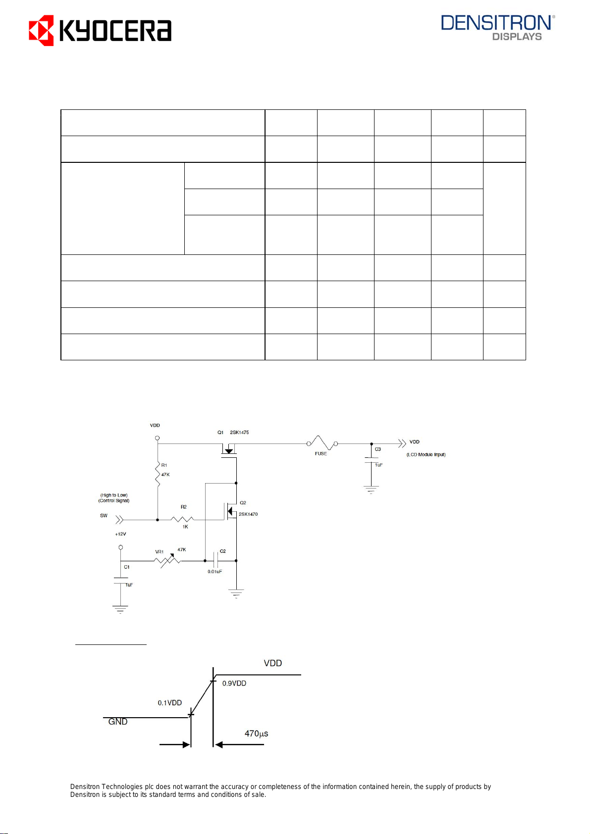
Rush current *1 IRUSH - - (1) A
Input signal voltage (Low) V - - 0.3VDD VIL
Input signal voltage (High) V 0.7VDD - VDD VIH
* The module is recommended to operate within specification ranges listed above for normal
function.
*1 Measurement Conditions :
VDD rising time
-4-
Page 8

Densitron Technologies plc does not warrant the accuracy or completeness of the information contained herein, the supply of products by
Densitron is subject to its standard terms and conditions of sale.
*2 The specified power supply current is under the conditions at VDD = 3.3V, Ta = 25℃,
Fr=60Hz
a. White Pattern b. Black Pattern
c.Vertical Stripe Pattern
5-2. Supply Voltage Sequence Condition
To prevent a latch-up or DC operation of LCD module, the power on/off sequence should be as
the diagram below.
* Timing Characteristics 0.5 < t1 ≦ 10ms
0 < t2 ≦ 50ms
0 < t3 ≦ 50ms
t4 ≧ 500ms
* Control the supply voltage sequence not to float all signal line when the LCD panel is
driving.
-5-
Page 9

Densitron Technologies plc does not warrant the accuracy or completeness of the information contained herein, the supply of products by
Densitron is subject to its standard terms and conditions of sale.
6.Optical Characteristics
ITEM SYMBOL CONDITION MIN TYP MAX UNIT
Response Rise τr θ=φ=0゜ - (14) - ms
time
Down τd θ=φ=0゜ - (9) - ms
Upper - (85) -
θ deg.
Lower - (85) -
Viewing angle range CR≧5
Left - (85) -
φ deg.
Right - (85) -
Contrast ratio CR θ=φ=0゜ (600) (750) - -
Measuring points = φ6.0mm , Temp. = 25℃
Brightness L IL=5.0mArms. (360) (450) - cd/m
Brightness uniformity LU - (70) - - %
x (TBD) (TBD) (TBD)
Red θ=φ=0゜
y (TBD) (TBD) (TBD)
x (TBD) (TBD) (TBD)
Green θ=φ=0゜
y (TBD) (TBD) (TBD) -
Chromaticity
coordinates x (TBD) (TBD) (TBD)
Blue θ=φ=0゜
y (TBD) (TBD) (TBD)
x (TBD) (TBD) (TBD)
White θ=φ=0゜
y (TBD) (TBD) (TBD)
6-1. Contrast ratio is defined as follows:
Brightness at all pixels "White"
CR =
Brightness at all pixels "Black"
2
6-2. Definition of viewing angle
0
=
θ
φ=0°
Y
+
X
-
-
θ
θ
+
( θ direction )
X
+
-
Y
-
-6-
+
Y
X
°
+
φ
φ
-
X
+
-Y
d
(
φ
)
i
r
e
c
t
i
o
n
Page 10

Densitron Technologies plc does not warrant the accuracy or completeness of the information contained herein, the supply of products by
Densitron is subject to its standard terms and conditions of sale.
6-3. Definition of brightness and brightness uniformity
The brightness is measuring by white brightness at center of display screen(3).
The brightness uniformity is calculated by using following formula.
Minimum brightness from 1 to 5
Brightness uniformity = × 100 [%]
Maximum brightness from 1 to 5
160×3 320×3 480×3 (dot)
14
120 ○ ○
3
240 ○
25
360 ○ ○
(dot)
1) Rating is defined as the average brightness inside the viewing area.
2) 30 minutes after CFL is turned on. (Ambient Temp.=25℃)
3) The inverter should meet the CFL rating conditions;
-Sine, symmetric waveform without spike in positive and negative.
-7-
Page 11

Densitron Technologies plc does not warrant the accuracy or completeness of the information contained herein, the supply of products by
Densitron is subject to its standard terms and conditions of sale.
7. Interface signals
7-1. LCD
CM1
1 GND GND -
CK Clock signal for sampling each data signal I2
Hsync Horizontal synchronous signal (negative) I3
Vsync Vertical synchronous signal (negative) I4
GND GND -5
R0 RED data signal (LSB) I6
R1 RED data signal I7
R2 RED data signal I8
R3 RED data signal I9
10 R4 RED data signal I
11 R5 RED data signal (MSB) I
12 GND GND 13 G0 GREEN data signal (LSB) I
14 G1 GREEN data signal I
15 G2 GREEN data signal I
G3 GREEN data signal I16
G4 GREEN data signal I17
G5 GREEN data signal (MSB) I18
GND GND -19
B0 BLUE data signal (LSB) I20
B1 BLUE data signal I21
B2 BLUE data signal I22
B3 BLUE data signal I23
B4 BLUE data signal I24
B5 BLUE data signal (MSB) I25
26 -GND GND
DE Signal to settle the horizontal display position(positive) I27
VDD power supply(+3.3V/+5.0V) -28
VDD power supply(+3.3V/+5.0V) -29
30 *1NC No connect I
31 (GND or Open : normal, High : Reverse) *2SC Scan direction control I
LCD side connector : DF9C-31P-1V(32) (HIROSE)
Recommended matching connector : DF9-31S-1V, DF9A-31S-1V(32) (HIROSE)
DF9B-31S-1V(32),DF9C-31S-1V(32) (HIROSE)
NotePIN NO. SYMBOL DESCRIPTION I/O
* The shield case is connected with GND.
*1 Do not input any signal at Pin No.30(Open state). It might happen LCD has a trouble.
*2 Scanning Direction
SC : GND or Open SC : High
7-2. CFL
CN2
PIN NO. SYMBOL DESCRIPTION
1 COLD Inverter output low voltage side
2 HOT Inverter output High voltage side
3 HOT Inverter output High voltage side
LCD side connector : BHR-03VS-1 (JST)
Recommended matching connector : SM03(4.0)B-BHS-1TB (JST)
: SM03(4.0)B-BHS-1-TB(LF)(SN) (JST)・・・(RoHS)
* Please be careful NOT to connect inversely an inverter-output high voltage side to the CFL low
voltage side. It may result in damage or electric shock.
-8-
Page 12

Densitron Technologies plc does not warrant the accuracy or completeness of the information contained herein, the supply of products by
Densitron is subject to its standard terms and conditions of sale.
. Timing Characteristics of input signals8
8-1. Timing characteristics
ITEM SYMBOL MIN TYP MAX UNIT NOTE
Frequency 1/Tc (21) (25.175) (29) MHz
Clock
Duty ratio - (0.4) (0.5) (0.6) -
Set up time Tds (8) - - ns
Data
Hold time Tdh (12) - - ns
Horizontal sync. Cycle TH (690) (800) (1,279) clock *1
signal
Display THd (640) (640) (640) clock
Blank THb (80) (160) (TH-THd) clock
Vertical sync. Frame frequency Fr (56) (60) (75) Hz
signal
Cycle TV (482) (525) (959) line *2
Display TVd (480) (480) (480) line
Blank TVb (2) (45) (TV-TVd) line
* In case of lower frequency, the deterioration of the display quality, flicker etc., may occur.
*1 TH = THd + THb
*2 TV = TVd + TVb
*3 Input signal timing diagram
-9-
Page 13

Densitron Technologies plc does not warrant the accuracy or completeness of the information contained herein, the supply of products by
Densitron is subject to its standard terms and conditions of sale.
8-2. Block diagram
9. Backlight Characteristics
Temp. = 25℃
ITEM SYMBOL MIN. TYP. MAX. NOTE
Starting - - (1,325) Vrms. -10 ℃
discharge Voltage *1 - - (830) Vrms. 25 ℃
Discharging tube current *2 IL (2.0) mArms. (5.0) mArms. (6.0) mArms. -
Discharging tube voltage VL - (490)Vrms. - IL=5.0mArms.
Operating life *3 T (36,000) h (50,000) h - IL=5.0mArms.
Operating frequency *4 F (40) kHz - (100) kHz -
*1 The Non-load output voltage (VS) of the inverter should be designed to have some margin,
because VS may increase due to the leak current which may be caused by wiring of CFL cables.
(Reference value : (1,720) Vrms Min.)
*2 We recommend that you should set the discharging tube current at lower than typical value
so as to prevent the heat accumulation of CFL tube from deteriorating a performance of the LCD.
*3 End of life is defined as when the illuminance or quantity of light has decreased to 50% of the
initial value. Illuminance of light will drastically decrease when LCD is operated at lower
temperature for long hours.
VS
*4 The driving frequency of the CFL may interfere with the horizontal synchronous signal ,leaving
interference stripes on the display. So please evaluate LCD panels beforehand.
To avoid interference stripes, we recommend to separate as far as possible the CFL frequency
from the horizontal synchronous signal and its high harmonic frequency.
* There may be cases where interface noise on LCD PCB, generated by high-voltage products such as
inverters, may leave stripes on the display. Please be careful when designing a mold to take
into consideration that the inverter shall be located as far as possible from PCB. Shield
protection may be effective.
-10-
Page 14

Densitron Technologies plc does not warrant the accuracy or completeness of the information contained herein, the supply of products by
Densitron is subject to its standard terms and conditions of sale.
10.Lot Number Identification
The lot number shall be indicated on the back of the backlight case of each LCD.
TCG104VG2AA-G00 - □ □-□ □ - □ MADE IN □□□□□
↓↓ ↓ ↓ ↓
①② ③ ④ ⑤
①YEAR
②MONTH
③DATE
④Version Number
⑤Country of origin(Japan or China)
YEAR 2006 2007 2008 2009 2010 2011
CODE 678901
MONTH JAN. FEB. MAR. APR. MAY. JUN.
CODE 123456
MONTH JUL. AUG. SEP. OCT. NOV. DEC.
CODE 789XYZ
11.Warranty
11-1. Incoming inspection
Please inspect the LCD within one month after your receipt.
11-2. Production Warranty
Kyocera warrants its LCDs for a period of 12 months after receipt by the purchaser, and within
the limits specified. Kyocera shall, by mutual agreement, replace or rework defective LCDs
that are shown to be Kyocera's responsibility.
-11-
Page 15

Densitron Technologies plc does not warrant the accuracy or completeness of the information contained herein, the supply of products by
Densitron is subject to its standard terms and conditions of sale.
12.Precautions for use
12-1. Installation of the LCD
1. A transparent protection sheet shall be added to protect the LCD and its polarizers.
2. The LCD shall be installed so that there is no pressure on the LSI chips.
3. The LCD shall be installed flat, without twisting or bending.
4. The display window size should be the same as the effective viewing area.
5. In case you use outside frame of effective viewing area as outward appearance of your product,
unevenness of its outward appearance is out of guarantee.
6. Do not pull the CFL lead wires and do not bend the root of the wires.
Housing should be designed to protect CFL lead wires from external stress.
12-2. Static Electricity
1. Since CMOS ICs are mounted directly onto the LCD glass, protection from static electricity is
required. Operator should wear ground straps.
12-3. LCD Operation
1. The LCD shall be operated within the limits specified. Operation at values outside of these
limits may shorten life, and/or harm display images.
2. Operation of the LCD at temperature below the limit specified may cause image degradation
and/or bubbles.
It may also change the characteristics of the liquid crystal.
This phenomenon may not recover. The LCD shall be operated within the temperature limits
specified.
12-4. Storage
1. The LCD shall be stored within normal temperature and humidity.
Store in a dark area, and protected the LCD from direct sunlight or fluorescent light.
2. Always store the LCD so that it is free from external pressure onto it.
12-5. Screen Surface
1. DO NOT store in a high humidity environment for extended periods.
Image degradation, bubbles, and/or peeling off of polarizer may result.
2. The front polarizer is easily scratched or damaged.
Prevent touching it with any hard material, and from being pushed or rubbed.
3. The LCD screen may be cleaned with a soft cloth or cotton pad.
Methanol, or Isopropyl Alcohol may be used, but insure that all solvent residue is removed.
4. Water may cause damage or discoloration of the polarizer.
Clean any condensation or moisture from any source immediately.
5. Always keep the LCD free from condensation during testing.
Condensation may permanently spot or stain the polarizers.
6. Do not disassemble LCD module because it will result in damage.
7. Please do not use solid-base image pattern for long hours because a temporary afterimage may
appear. We recommend to use screen saver etc. in cases where a solid-base image pattern must
be used.
8. A transparent protection sheet is attached to the polarizer. Please remove the protection
film slowly before use, paying attention to static electricity.
9. This Kyocera LCD module has been specifically designed for use in general electronic devices,
but not for use in a special environment such as usage in an active gas.
Hence, when the LCD is supposed to be used in a special environment, evaluate
the LCD thoroughly beforehand and do not expose the LCD to chemicals such as an active gas.
-12-
Page 16

Densitron Technologies plc does not warrant the accuracy or completeness of the information contained herein, the supply of products by
Densitron is subject to its standard terms and conditions of sale.
13.Reliability Data / Environmental Test
TEST TEST TEST RESULT
ITEM CONDITION TIME
High Temp. Display Quality : T.B.D.
Atmosphere 80℃ 240 h Display Function : T.B.D.
Current Consumption : T.B.D.
Low Temp. Bubble : T.B.D.
Solid Crystallization of
Low Temp. -30℃ 240 h Liquid Crystal : T.B.D.
Atmosphere Display Quality : T.B.D.
Display Function : T.B.D.
Current Consumption : T.B.D.
Display Quality : T.B.D.
High Temp. 60℃ 240 h Display Function : T.B.D.
Humidity 90 %RH Peel-off of Organic
Operation Sealing : T.B.D.
Current Consumption : T.B.D.
Display Quality : T.B.D.
Temp. Cycle -30℃ 0.5 h 10 cycles Display Function : T.B.D.
R.T. 0.5 h Peel-off of Organic
80℃ 0.5 h Sealing : T.B.D.
Bubble on Cell : T.B.D.
High Temp. 70℃ 500 h Display Quality : T.B.D.
Operation Current Consumption : T.B.D.
* Each test item uses a test LCD only once. The tested LCD is not used in any other tests.
* The LCD is tested in circumstances in which there is no condensation.
* The tested LCD is inspected after 24 hours of storage at room temperature and room humidity
after each test is finished.
* The reliability test is not an out-going inspection.
* The results of the reliability test are for your reference purpose only.
The reliability test is conducted only to examine the LCD's capability.
-13-
Page 17

Densitron Technologies plc does not warrant the accuracy or completeness of the information contained herein, the supply of products by
Densitron is subject to its standard terms and conditions of sale.
Page 18

Densitron Technologies plc does not warrant the accuracy or completeness of the information contained herein, the supply of products by
Densitron is subject to its standard terms and conditions of sale.
Page 19

Densitron Technologies plc does not warrant the accuracy or completeness of the information contained herein, the supply of products by
Densitron is subject to its standard terms and conditions of sale.
Page 20

Densitron Technologies plc does not warrant the accuracy or completeness of the information contained herein, the supply of products by
Densitron is subject to its standard terms and conditions of sale.
Date
Rev. No. Date Page Descriptions
Designed by: Engineering Dept. Confirmed by: QA Dept.
Prepared Checked Approved Checked Approved
Revision Record
Page 21

Densitron Technologies plc does not warrant the accuracy or completeness of the information contained herein, the supply of products by
Densitron is subject to its standard terms and conditions of sale.
1) Note
1) Note
1) Note1) Note
General 1. Customer identified anomalies not defined within this inspection standard
Definition of Dot defect Bright dot defect The dot is constantly "on" when power
Inspection item applied to the LCD, even when all "Black"
shall be reviewed by Kyocera, and an additional standard shall be
determined by mutual consent.
2. Inspection Conditions
Luminance :500 Lux minimum
Inspection distance :300 mm (from the sample)
Temperature :25 ± 5 ℃
Direction :directly above
Note
data sent to the screen.
Inspection tool:5% Transparency neutral
density filter .
Count dot:If the dot is visible through
the filter
Don't count dot:If the dot is not visible
through the filter.
RGBRGBRGB
RGBRGBRGB
RGBRGBRGB
Black dot defect The dot is constantly "off" when power
applied to the LCD, even when all "white"
data sent to the screen.
Adjacent dot Adjacent dot defect is defined as two or
more bright dot defects or black dot
defects.
RGBRGBRGB
RGBRGBRGB
RGBRGBRGB
External Bubble,Scratches, Visible operating (all pixcels "Black"
inspection Foreign particle or "White") and non operating.
(Polarizer, Cell,
Backlight)
Appearance Does not satisfy the value at the spec.
inspection
Others CFL wires Damaged to the CFL wires, connector, pin,
functional failure or appearance failure.
dot defect
dot defect
Definition Definition of circle size Definition of linear size
of size
d=
d=
d=d=
aaaa
(a+b)
(a+b)
(a+b)(a+b)
b
bb
b
LLLL
2222
-1-
WWWW
Page 22

Densitron Technologies plc does not warrant the accuracy or completeness of the information contained herein, the supply of products by
Densitron is subject to its standard terms and conditions of sale.
2) Standard
2) Standard
2) Standard2) Standard
Classification Inspection item Judgement standard
defect Dot Bright dot defect Acceptable number : 4 bright dots defects
(in LCD defect Bright dot spacing : 5 mm or more
glass)
Black dot defect Acceptable number : 5 black dots defects
Black dot spacing : 5 mm or more
2 dots join defect
3 or more dots join Acceptable number : 0
Total dot defects Acceptable number : 5 Max
Others White dot, Dark dot
(Circle)
External Polarizer(Scratches)
inspection Width(mm) Length(mm) Acceptable Number
(Defect on
Polarizer or W≦0.1 - (neglected)
between Polariz
-er and LCD L≦5.0 (neglected)
glass) 0.1<W≦0.3
Bright dot Acceptable number : 2
Black dot Acceptable number : 3
defect
Size(mm) Acceptable Number
d<0.2 (neglected)
0.2<d≦0.4 5
0.4<d≦0.5 3
0.5<d0
5.0<L0
0.3<W- 0
Polarizer Touch panel
(Bubble, Dent) Size(mm) Acceptable Number
d<0.2 (neglected)
0.2<d≦0.3 5
0.3<d≦0.5 3
0.5<d0
Foreign Particle(Circular
shape) Size(mm) Acceptable Number
d<0.2 (neglected)
0.2<d≦0.4 5
0.4<d≦0.5 3
0.5<d0
Foreign Particle
(Linear shape), Width(mm) Length(mm) Acceptable Number
Scratches
W≦0.03 - (neglected)
L≦2.0 (neglected)
0.03<W≦0.1 2.0< L≦4.0 3
4.0<L0
0.1<W - (According to
-2-
Circular shape)
 Loading...