How it Works
Log In / Sign Up
Buy Points
How it Works
FAQ
Contact Us
Questions and Suggestions
Users
KYOCERA
Loading...
T
TASKalfa300
70
TASKalfa400
70
TASKALFA 400CI
46
TASKalfa 4012i
2
TASKalfa 4052ci
4
Taskalfa 4053ci
TASKalfa 406ci
2
TASKalfa 420i
24
TASKalfa 4500i
18
TASKalfa 4501i
8
TASKALFA 4550CI
20
Taskalfa 4551 ci
7
TASKalfa 4820w
5
TASKalfa 5002i
3
Taskalfa 5003i
TASKalfa500ci
114
TASKalfa 5052ci
4
Taskalfa 5053ci
TASKALFA 520I
25
TASKalfa 5500i
18
TASKalfa 5501i
7
TASKALFA 550C
46
TASKalfa 552
TASKalfa 552ci
63
TASKALFA 5550CI
21
Taskalfa 5551 ci
6
TASKalfa 6002i
4
Taskalfa 6003i
TASKalfa 6052ci
4
Taskalfa 6053ci
TASKalfa 620
27
TASKalfa 6500i
14
TASKalfa 6501i
7
TASKalfa 650c
32
TASKalfa 6550ci
17
TASKalfa 6551ci
2
TASKalfa 7002i
TASKalfa 7052ci
2
TASKalfa 750c
44
TASKalfa 7550ci
13
TASKalfa 7551ci
2
TASKalfa 8000i
17
TASKalfa 8001i
8
TASKalfa 8002i
TASKalfa 8052ci
2
TASKALFA 820
33
TASKalfa 9002i
TASKalfa FAX SYSTEM V
TASKALFA FS-1100
TASKALFA FS-1300D
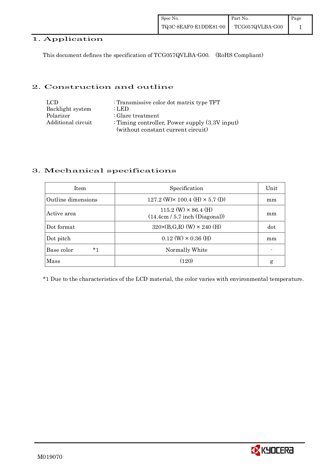
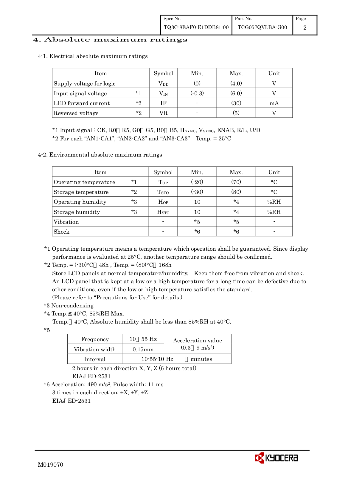
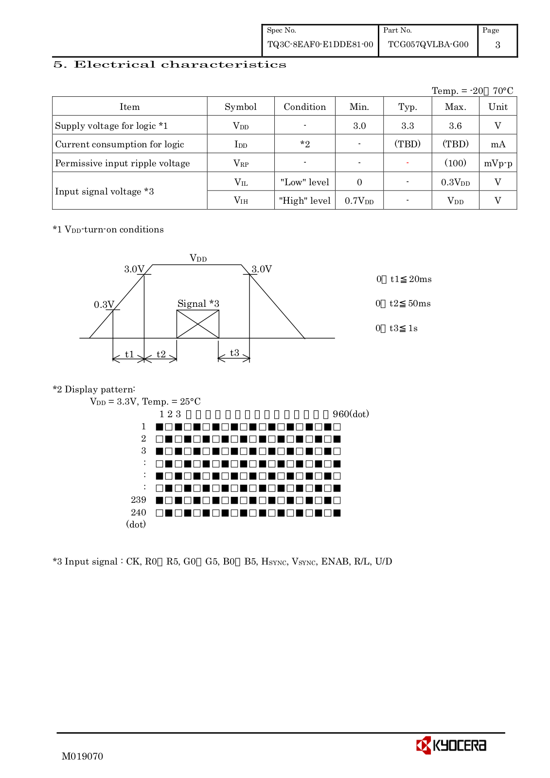
TCG057QVLBA-G00
TCG057VGLBA-G00
TCG104VG2AA-G00
TCG121SVLPAANN-AN20
TCG121SVLPBANN-AN00
TCG121SVLQXPNN-ANX12
TCG150XGLBA-A00
TCG150XGLBB-C00
TCG190SX4AA-A00
TCG190SX4AB-A00
Teaching Assistant
Tempo
Tempo E2000
THINPHONE
Tjep Ultra Grip 25
Tjep Ultra Grip 40
Tjep Ultra Grip 58
TK-1120
2
TK-1130
TK-1140
TK-1170
TK-160
TK-170
TK-3100
TK-3110
TK-3130
TK-3150
TK-410
TK-4105
TK-435
TK-475
TK-5220C
TK-5220K
TK-5220M
TK-5220Y
TK-5230C
TK-5230K
TK-5230M
TK-5230Y
TK-590C
TK-590K
TK-6305
TK-685
TK-8305C
TK-8305Y
TK-895C
TK-895Y
TNT!
2
TNT S2400
TNT VMS200
Loading...
Loading...
Nothing found
TCG057QVLBA-G00
Specification
20 pgs
598.94 Kb
0
Table of contents
Loading...
KYOCERA TCG057QVLBA-G00 Specification
...
KYOCERA Specification
Download
Specifications and Main Features
Frequently Asked Questions
User Manual
Download
Loading...
+
14
hidden pages
Unhide
You need points to download manuals.
1 point = 1 manual.
You can buy points or you can get point for every manual you upload.
Buy points
Upload your manuals
 Loading...