

Page 1
User Manual
KUNBUS-COM EtherCat
PR100033 • 16/09/2015
Page 2

Table of Contents KUNBUS GmbH
ii KUNBUS-COM EtherCAT
Table of Contents
1 General information ........................................................................................................................4
1.1 Disclaimer..................................................................................................................................4
1.2 Notes regarding this user manual..............................................................................................4
1.3 Validity.......................................................................................................................................5
1.4 Limitation of Liability ..................................................................................................................5
1.5 Customer Service......................................................................................................................5
2 Safety Guidelines ............................................................................................................................6
2.1 User...........................................................................................................................................6
2.2 Symbols.....................................................................................................................................6
2.3 General Safety Guidelines.........................................................................................................7
2.4 Environmental Conditions..........................................................................................................7
3 Overview ..........................................................................................................................................8
3.1 Introduction................................................................................................................................8
3.2 Spacer bolt ................................................................................................................................9
3.3 Application Interface................................................................................................................11
3.4 Fieldbus Connection Socket....................................................................................................15
3.5 Status LEDs.............................................................................................................................16
4 Components ..................................................................................................................................18
4.1 Module Components ...............................................................................................................18
4.2 Storage Unit.............................................................................................................................19
4.3 Data Broker .............................................................................................................................20
4.4 Fieldbus Interface....................................................................................................................28
4.5 CDI - Configuration and Debug Interface................................................................................28
4.6 DPR - Dual Port RAM..............................................................................................................29
4.7 SDI - Serial Data Interface.......................................................................................................31
4.8 Synchronous serial interface ...................................................................................................32
4.9 Scripter ....................................................................................................................................44
5 Commissioning .............................................................................................................................45
5.1 Installation ...............................................................................................................................45
5.2 Configuration ...........................................................................................................................46
5.3 Firmware Update.....................................................................................................................46
6 Memory Register ...........................................................................................................................47
6.1 Overview of the Memory Register ...........................................................................................47
6.2 General Device Parameters ....................................................................................................50
6.3 Register for the Mapping .........................................................................................................75
6.4 Memory of the Communication Channels ...............................................................................78
6.5 Fieldbus specific Registers......................................................................................................81
6.6 Reserve Register.....................................................................................................................89
Page 3

KUNBUS GmbH Table of Contents
KUNBUS-COM EtherCAT iii
7 Communication model .................................................................................................................90
7.1 EtherCAT Object Directory......................................................................................................90
8 CDI .................................................................................................................................................93
8.1 Setting up a Serial Connection................................................................................................93
8.2 CDI Menus...............................................................................................................................96
9 Disposal .......................................................................................................................................132
9.1 Dismantling and Disposal......................................................................................................132
10 Technical data .............................................................................................................................133
10.1Technical data .......................................................................................................................133
11 Appendix ......................................................................................................................................134
11.1Configuration via Modpoll ......................................................................................................134
Page 4

KUNBUS-COM EtherCAT
4 / 135
1 General information
1.1 Disclaimer
© 2015 KUNBUS GmbH, Denkendorf (Deutschland)
The contents of this user manual have been prepared by the
KUNBUS GmbH with the utmost care. Due to the technical
development, the KUNBUS GmbH reserves the right to change or
replace the contents of this user manual without prior notice. You can
always obtain the latest version of the user manual at our homepage:
www.kunbus.de
The KUNBUS GmbH shall be liable exclusively to the extent
specified in General Terms and Conditions (www.kunbus.de/
agb.html).
The contents published in this user manual are protected by
copyright. Any reproduction or use for the in-house requirements of
the user is permitted. Reproduction or use for other purposes are not
permitted without the express, written consent of the KUNBUS
GmbH. Contraventions shall result in compensation for damages.
Trademark protection
– KUNBUS is a registered trademark of the KUNBUS GmbH
– Windows® and Microsoft® are registered trademarks of the Microsoft,
Corp.
– Modbus is a registered trademark of the Modbus-IDA Organization.
KUNBUS GmbH
Heerweg 15 c
73770 Denkendorf
Deutschland
www.kunbus.de
1.2 Notes regarding this user manual
This user manual provides important technical information that can
enable you, as a user, to efficient, safe and convenient integration of
the COMS-Module into your applications and systems. It is intended
for trained, qualified personnel, whose sound knowledge in the field
of electronic circuits and expertise of EtherCATTM is assumed.
As an integral part of the module, the information provided here
should be kept and made available to the user.
General information
Page 5

KUNBUS-COM EtherCAT 5 / 135
1.3 Validity
This document describes the application of the KUNBUS COMSModuls with the product number:
– PR100033, Release 02
1.4 Limitation of Liability
Warranty and liability claims will lapse if:
– the product has been used incorrectly,
– damage is due to non-observance of the operating manual,
– damage is caused by inadequately qualified personnel,
– damage is caused by technical modification to the product (e.g.
soldering).
1.5 Customer Service
If you have any questions or suggestions concerning this product,
please do not hesitate to contact us:
KUNBUS GmbH
Heerweg 15 C
+49 (0)711 3409 7077
support@kunbus.de
www.kunbus.de
General information
Page 6

KUNBUS-COM EtherCAT
6 / 135
2 Safety Guidelines
2.1 User
The Modul may only be assembled, installed and put into operation
by trained, qualified personnel. Before assembly, it is absolutely
essential that this documentation has been read carefully and
understood. Expertise in the following fields is assumed:
– Electronic circuits,
– Basic knowledge of EtherCAT,
– work in electrostatic protected areas,
– Locally applicable rules and regulations for occupational safety.
2.2 Symbols
The symbols used have the following meaning:
DANGER
Hazard
Observe this information without fail!
There is a safety hazard that can lead to serious injuries and death.
CAUTION
Caution
There is a safety hazard that can result in minor injuries and material
damage.
NOTICE
Note
Here you will find important information without a safety hazard.
Safety Guidelines
Page 7

KUNBUS-COM EtherCAT 7 / 135
2.3 General Safety Guidelines
DANGER
Danger of electric shock
If unsuitable power supply is used, this can cause an electric shock.
Ø This can cause death, serious injuries and material damage to your
systems and modules.
èOnly use a power supply that complies with the regulations for safety
extra-low voltage (SELV) or protective extra-low voltage (PELV).
CAUTION
Fault due to mechanical load
A continuous mechanical load of over 5G or shock loads of over 15G can
cause faults on your modules.
èComply with these load limits and avoid any unnecessary loads.
CAUTION
Fault due to missing or unsuitable spacer bolt
Incorrect or missing spacer bolts can result in high mechanical loads on
your module and control board. This can cause faults.
èAlways use spacer bolts suitable for the connector height of the circuit
board so that the module does not lie on the circuit board.
You can find detailed information in section "Spacer bolt [}9]"
CAUTION
Damage due to subsequent processing
Avoid subsequent processing of theCOMS-Modul.
Ø Soldering can cause components to become detached and thus
damage or destroy the module.
Ø Please note that the warranty shall become invalid if the products are
changed technically.
èSpeak to your contact person at the KUNBUS GmbH about customised
solutions.
2.4 Environmental Conditions
Operate the COMS-Modul only in an environment that complies with
the operating conditions in order to prevent any damage.
Suitable Environmental Conditions:
Operating temperature 0 to +60°C
Humidity 0% not 95%, non-condensing
Safety Guidelines
Page 8
KUNBUS-COM EtherCAT
8 / 135
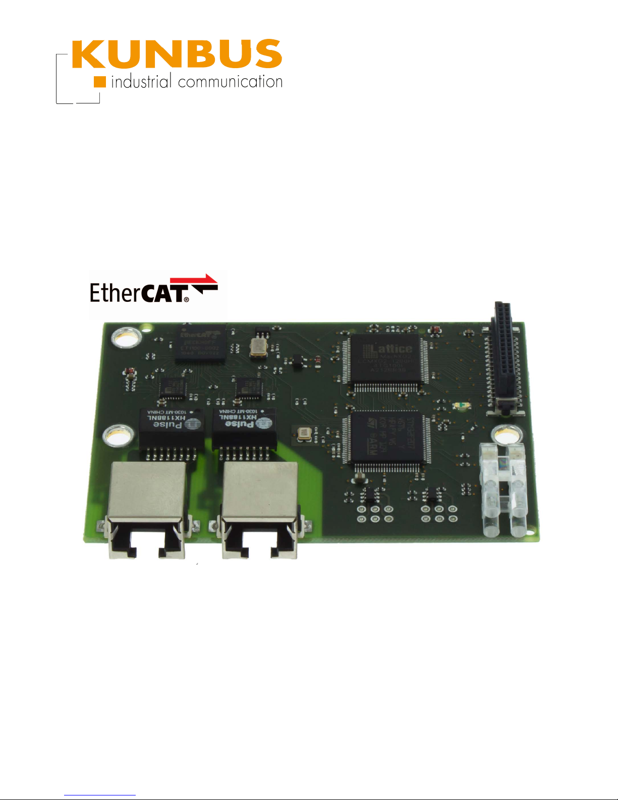
3 Overview
3.1 Introduction
With the KUNBUS COMS-Modul you can make a sensor or actuator
fieldbus-capable. To do this, simply insert the module into your
application and connect it to the fieldbus.
The COMS-Modul thereby saves you time-consuming in-house
developments.
Illustration1: Overall view
Overview
Page 9
KUNBUS-COM EtherCAT 9 / 135
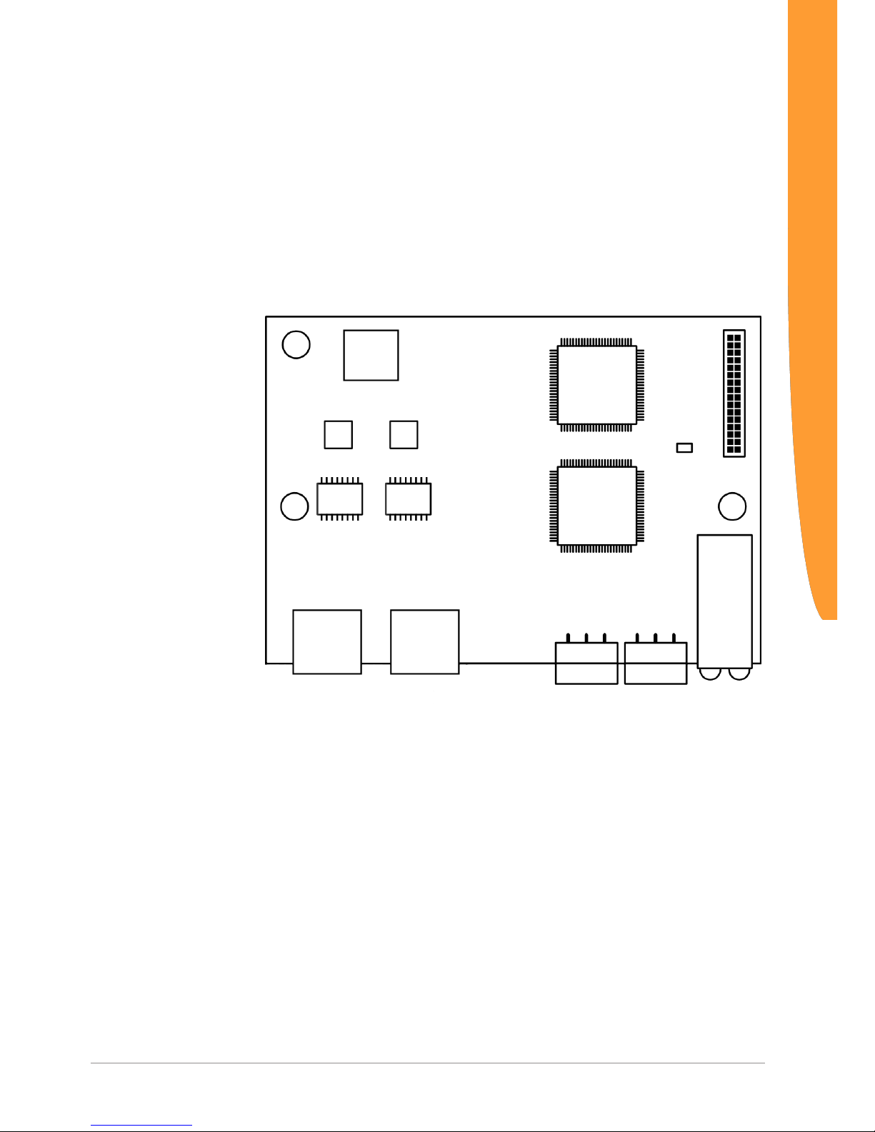
3.2 Spacer bolt
There are three holes on the module for spacer bolts. These spacer
bolts have 2 tasks:
– they stabilise the COMS module with a direct connection to the main
board
– they are part of the earthing concept.
Illustration2: Holes for spacer bolts
Suitable spacer bolts
Suitable spacer bolts have the following properties:
– Conductive material
– Holes for M3 screws
– Diameter: maximum 8mm
Connections
These spacer bolts are an important part of the earthing concept of
the COMS-Modul.
– Connect hole 1 to protective earth on the fieldbus side
– Hole 2 is not electrically connected.
– Connect the spacer bolts of hole 3 to GND (earth power supply)
Overview
Page 10

KUNBUS-COM EtherCAT
10 / 135
Height of spacer bolts
The height of the spacer bolts depends on the height of the plug
connector used on the application side.
We recommend using the ERNI 254589 plug connector. The spacer
height for this plug connection is 10.75 to 12.3 mm above the circuit
board.
WARNING
Fault due to missing or unsuitable spacer bolt
Incorrect or missing spacer bolts can result in high mechanical loads on
your module and control board. This can cause faults.
èAlways use spacer bolts suitable for the connector height of the circuit
board so that the module does not lie on the circuit board.
Overview
Page 11
KUNBUS-COM EtherCAT 11 / 135
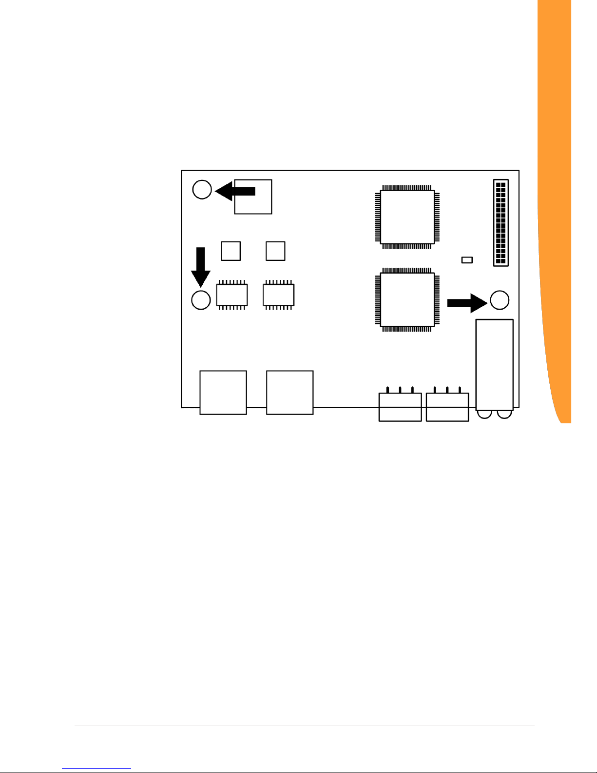
3.3 Application Interface
The main board is connected to the device controller via a 32-pin
connector strip. You have the option to plug the module in directly.
CAUTION
Mechanical loads can lead to faults on the module
èUse suitable spacer bolts to prevent mechanical loads. (e.g.
Ord.No.9774110360 from Würth Elektronik).
Illustration3: Application Interface
Pin assignment on the
application interface
The module can be operated in serial or parallel mode. In serial
mode you can choose whether you want to use the module as
master or slave.
You can activate the modes via logical levels:
Mode Switchover level
Serial slave mode "a14": +3.3V, "a6" +3.3V
Serial master mode "a14": +3.3V, "a6": 0V
Parallel mode "a"14" GND
You can change over the operating mode via pin a14.
Overview
Page 12

KUNBUS-COM EtherCAT
12 / 135
Slave Mode ("a14": +3.3V, "a6" +3.3V)
Pin Designation Direction Comment
a1 CDI.TX [OUT] Send CDI
a2 receive CDI.RX [IN] CDI
a3 GND Supply
a4 SPI.SCK [IN] SPI Clock
a5 SPI.MOSI [IN] SPI Data In
a6 SPI.MODE.DIR [IN] SPI Mode
1 = Slave
a7 SPI.MID [IN] SPI Middle
a8 UART.TX [OUT] Send SDI
a9 UART.TE [OUT] SDI 1 = transmitter activ-
ated
for RS485 operation
a10-a13 Reserved Do not connect!
a14 MODE [IN] Mode-Select
1 = Serial Mode
a15 RESET [IN] Module-Reset ( low-active )
a16 GND Supply
b1-b2 Reserved Do not connect!
b3 GND Supply
b4 SPI.MISO [OUT] SPI Data Out
b5 SPI.CS [IN] SPI Chip-Select
b6 SPI.READY [OUT] SPI Ready
b7 SPI.RESET [OUT] Reset signal for the SSC
b8 UART.RX [IN] Receive SDI
b9-b15 Reserved Do not connect!
b16 +3V3 Supply
Overview
Page 13

KUNBUS-COM EtherCAT 13 / 135
SSC Master ("a14": +3.3V "a6": 0V)
Pin Designation Direction Comment
a1 CDI.TX [OUT] Send CDI
a2 receive CDI.RX [IN] CDI
a3 GND Supply a4 SPI.SCK [OUT] SPI Clock
a5 SPI.MOSI [OUT] SPI Data Out
a6 SPI.MODE.DIR [IN] SPI Mode
0 = Master
a7 SPI.MID [IN] SPI Middle
a8 UART.TX [OUT] Send SDI
a9 UART.TE [OUT] SDI 1 = transmitter activ-
ated
for RS485 operation
a10-a13 Reserved Do not connect!
a14 MODE [IN] Mode-Select
1 = Serial Mode
a15 RESET [IN] Module-Reset ( low-active )
a16 GND Supply
b1-b2 Reserved Do not connect!
b3 GND Supply b4 SPI.MISO [IN] SPI Data In
b5 Reserved Do not connect!
b6 SPI.LOAD [OUT] Load signal for the SSC
b7 SPI.RESET [OUT] Reset signal for the SSC
b8 UART.RX [IN] Receive SDI
b9-b15 Reserved Do not connect!
b16 +3V3 Supply
Overview
Page 14

KUNBUS-COM EtherCAT
14 / 135
Parallel Operating Mode ("a"14" GND)
Pin Designation Direction Comment
a1 CDI.TX [OUT] Send CDI
a2 receive CDI.RX [IN] CDI
a3 GND Supply
a4 ADDR0 [IN] Address-Bit 0
a5 ADDR1 [IN] Address-Bit 1
a6 ADDR2 [IN] Address-Bit 2
a7 ADDR3 [IN] Address-Bit 3
a8 ADDR4 [IN] Address-Bit 4
a9 ADDR5 [IN] Address-Bit 5
a10 ADDR6 [IN] Address-Bit 6
a11 ADDR7 [IN] Address-Bit 7
a12 ADDR8 [IN] Address-Bit 8
a13 ADDR9 [IN] Address-Bit 9
a14 MODE [IN] Mode-Select
0 = Parallel Mode
a15 RESET [IN] Module-Reset ( low-active )
a16 GND Supply
b1-b2 Reserved Do not connect!
b3 GND Supply
b4 DATA0 [IN/OUT] Databus-Bit 0
b5 DATA1 [IN/OUT] Databus-Bit 1
b6 DATA2 [IN/OUT] Databus-Bit 2
b7 DATA3 [IN/OUT] Databus-Bit 3
b8 DATA4 [IN/OUT] Databus-Bit 4
b9 DATA5 [IN/OUT] Databus-Bit 5
b10 DATA6 [IN/OUT] Databus-Bit 6
b11 DATA7 [IN/OUT] Databus-Bit 7
b12 CS_B [IN] Chip-Select
(low-active)
b13 WR_B [IN] Write-Enable
(low-active)
b14 RD_B [IN] Read-Enable
(low-active)
b15 Reserved Do not connect!
b16 +3.3V Supply
Overview
Page 15

KUNBUS-COM EtherCAT 15 / 135
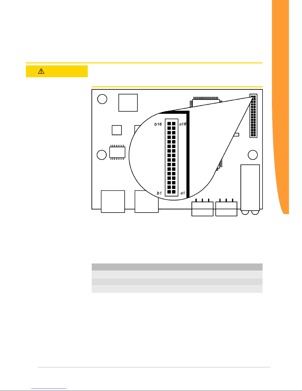
3.4 Fieldbus Connection Socket
The module has a two Ethernet sockets for connecting to the
fieldbus.
Illustration4: Fieldbus Connection Socket
Pin assignment forEtherCAT
Pin Assignment
1 TX+
2 TX3 RX+
4 Not assigned.
Pin 4 and 5 are interconnected and
laid via a filter on PE for better EMC
response.
5
6 RX7 Not assigned.
Pin 4 and 5 are interconnected and
laid via a filter on PE for better EMC
response.
8
Overview
Page 16
KUNBUS-COM EtherCAT
16 / 135
3.5 Status LEDs
The COMS-Module are fitted with LEDs for status indication.
Lightpipes guide the LED signals to the side.
Illustration5: Status LEDs
No. LED Status Meaning Note
1 Module Error
(red)
Off No error has
occurred
Flashing
Configuration
error
At least one system component
does not function due to a configuration error.
On Internal system
error
A fatal, internal error has occurred.
Flashing
Start-up phase At least one system component
has not yet finished the start-up
phase.
On A serious error
has occurred
A fatal error has occurred.
Overview
Page 17

KUNBUS-COM EtherCAT 17 / 135
2 Operating
Mode (green)
Off Module not
running
Flashing
Start-up phase At least one system component
has not yet finished the start-up
phase.
On Normal opera-
tion
All system components function
faultlessly.
3 Link Activity
OUT
off No connection
flashesConnection
and data traffic
on Connection
4 Link Activity IN off No connection
flashesConnection
and data traffic
on Connection
Overview
Page 18
KUNBUS-COM EtherCAT
18 / 135
4 Components
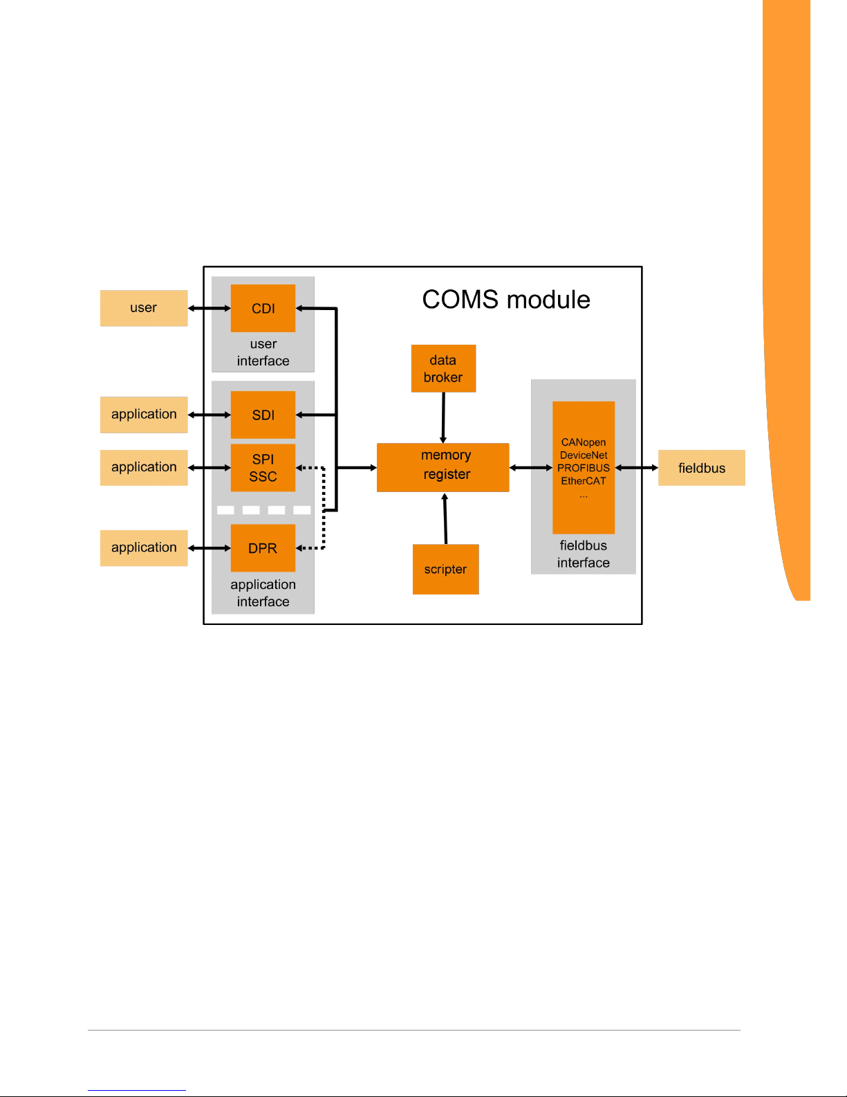
4.1 Module Components
The module is divided into independent components to ensure a high
level of flexibility in the application.
The following pages describe the individual components:
Illustration6: Components
Components
Page 19

KUNBUS-COM EtherCAT 19 / 135
4.2 Storage Unit
The storage unit is the central component for all functions of the
COMS-Module. It is subdivided into individual Memory Register with
a width of 16 bits each. In these Memory registers the following
information is stored:
– Input and output data
– Configuration settings
– Module Status
– Error states
The functionality of the addressing was incorporated from Modbus.
The register assignment depends on the application and is not
specified by the Modbus specification. A Memory Register according
to this specification has a register number between 1 (0x0001) and a
maximum of 65536 (0x10000), of which the module only uses a small
part, however.
With 8-bit values, 1 byte remains unused. 32-bit values are stored in
2 registers.
The 16-bit values are stored internally in the memory in Little Endian
order. This must be taken into account when you access data via the
fieldbus interface, SDI or SSC.
NOTICE!In the description of the individual memory registers
and CDI, the memory registers are also referred to as Modbus
registers.
In section Overview of the Memory Register [}47] we have
compiled a detailed overview of registers for you.
Components
Page 20
KUNBUS-COM EtherCAT
20 / 135
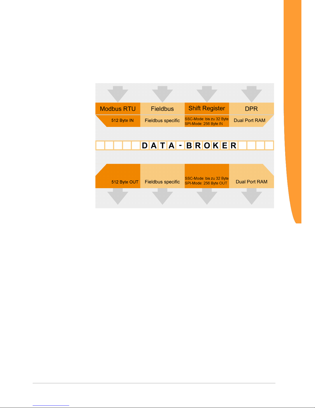
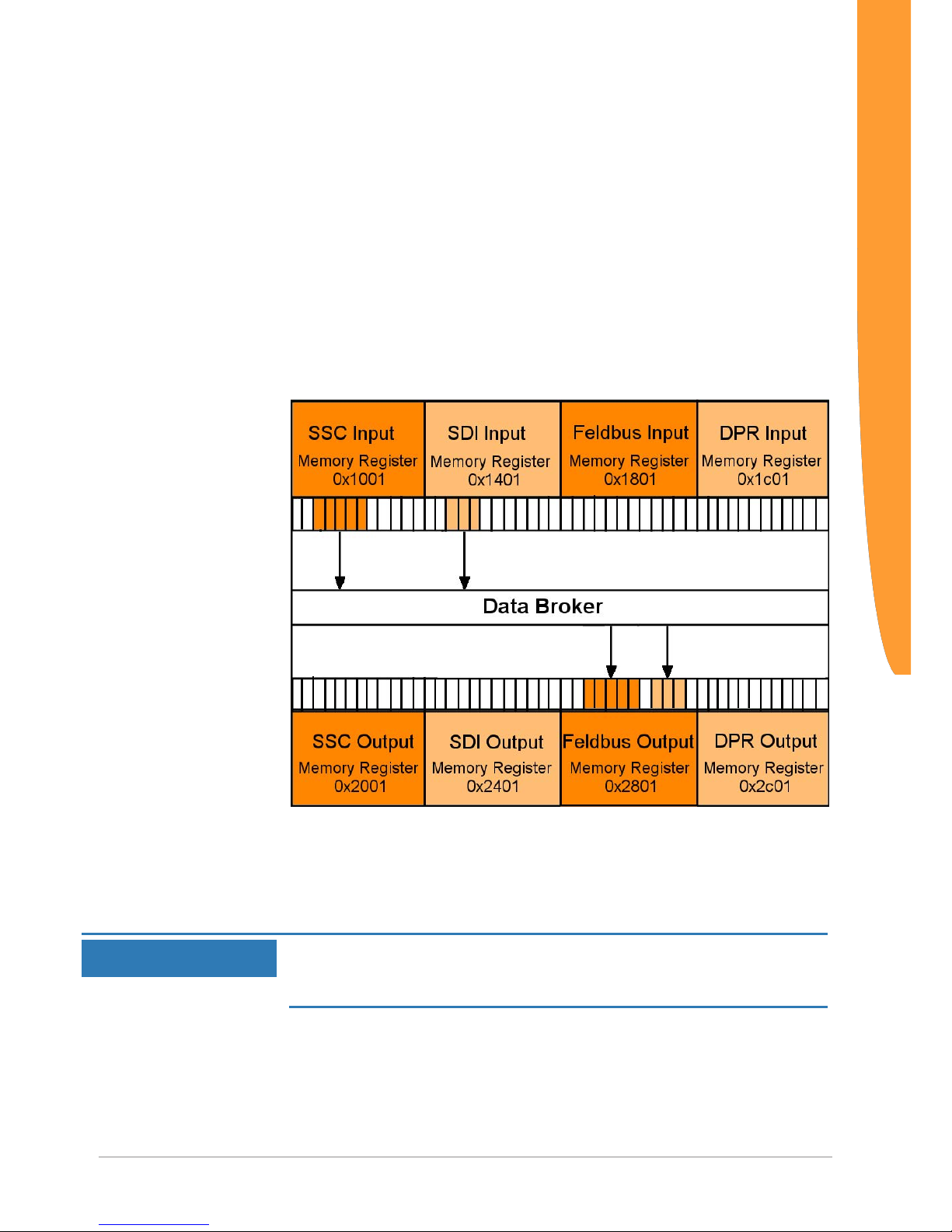
4.3 Data Broker
The Data Broker decouples individual components from each other
and distributes the data streams between the interfaces. The
targeted forwarding of the data ensures a high level of functionality
between the data sources and data sinks of the module.
Illustration7: Internal mapping by the Data Broker
Mapping
You have the option to define the allocation (mapping) yourself. This
allows you to define which input register the Data Broker should
accept data from and which output register it should transfer data to.
You can define up to 8 register areas with freely definable lengths in
the respective output register area for each of the interfaces. Any
register area of the same length is assigned to the output register
areas from one of the input register areas of all interfaces. Here, the
8 target areas are always on consecutive output register positions,
starting with the lowest register address for the respective interface.
Components
Page 21
KUNBUS-COM EtherCAT 21 / 135
Illustration8: Mapping
NOTICE
Viewpoint
Please note that the description of the input and output values is written
from the perspective of the module and not from the perspective of the
overall system or controller.
èOutput: Values that the module sends to the fieldbus or application.
èInput: Values that the module receives from the fieldbus or application.
You can configure standard values that the Data Broker writes in the
relevant output register instead of an input register in the event of a
failure of a data provider. That has the advantage that the data
processing cannot abort uncontrollably.
The module uses the Little Endian byte order for the internal
processing. You can also configure the Data Broker so that it
exchanges the high and low byte when copying if necessary. To do
this, add the value 0x8000 or 32768 for the required mapping area
(see details below).
Extended Mapping
Some applications work with data that is viewed bit by bit. To make
the mapping for such applications even more flexible, an "Extended
Mapping" is provided. This mapping basically works in the same way
as the mapping described above:
Components
Page 22
KUNBUS-COM EtherCAT
22 / 135
Individual areas of the output Memory Register are assigned from
areas of the input Memory registers. In Extended Mapping you define
such assignments for up to 16 areas. When doing so, enter a number
of consecutive bits for each of these areas.
The limit of a register must not be exceeded: The area may be up to
1024 bits long. Unlike the simple mapping described above,
however, the 16 target areas do not necessarily have to be at
consecutive addresses. You are totally free to define the position of
the first bit of the target area by entering an output register address
and the corresponding bit position (0 to 15). The source area is also
defined by entering the input register and a start bit position.
Illustration9: Extended Mapping
All mapping areas are processed sequentially. The Data Broker first
copies all simple mapping areas cyclically. After that, it executes the
Extended Mapping. In the course of this, it is quite possible to
intentionally overwrite a target area by several sources of data.
NOTICE
It is possible that bits are overwritten unintentionally by various input
sources.
Make sure that the target areas do not overlap unintentionally.
Components
Page 23
KUNBUS-COM EtherCAT 23 / 135
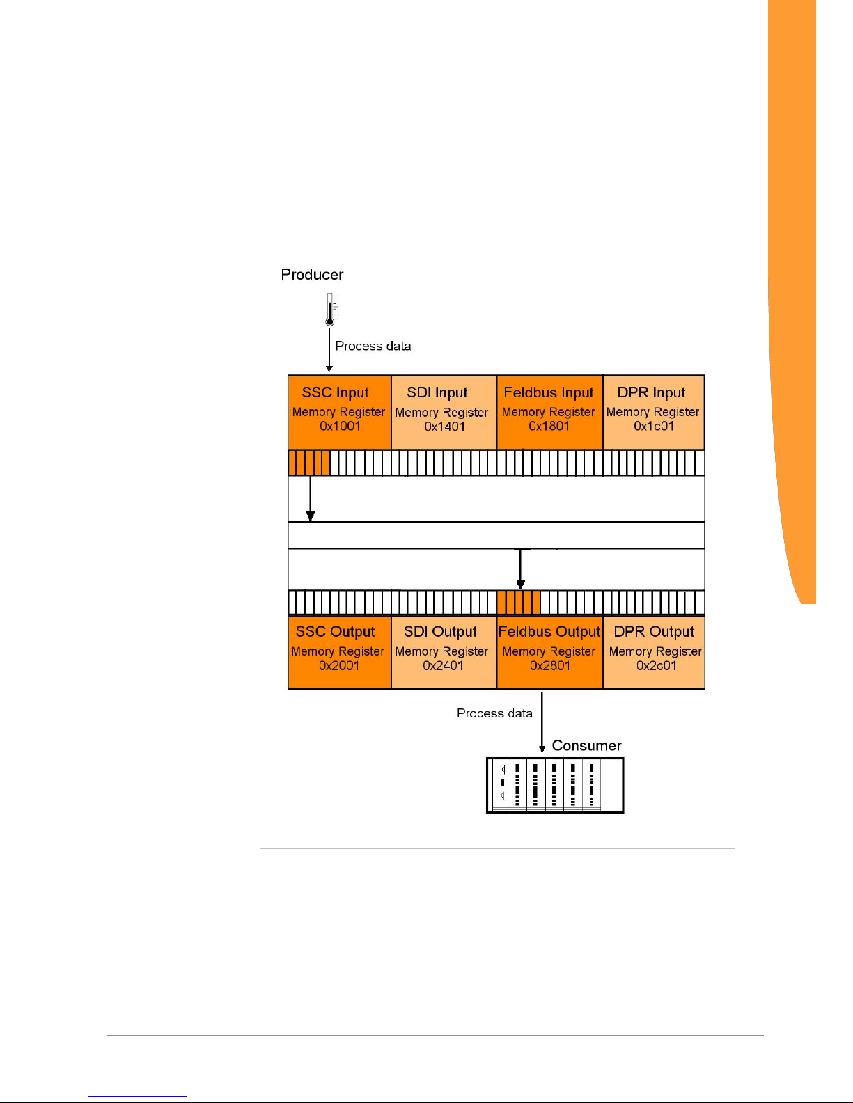
Validity period of the process data
Data sources that write data to the input area of the central memory
are called producers because they produce process data. The Data
Broker collects this data and copies it into the output area of the
central memory. From there, the data is sent to its target, the socalled consumer, via the corresponding interfaces.
Illustration10: Distribution to producers/consumers
Process data is normally exchanged cyclically between producers
and consumers. If a producer fails (e.g. a connector is removed or a
cable is broken), the consumer must be able to deal with this
situation appropriately. For this reason, you can define in advance
which values the producer will receive in exchange for the failed
process data.
Components
Page 24

KUNBUS-COM EtherCAT
24 / 135
The COMS-Module allow a separate validity period to be defined for
each producer (SDI, SSC, EtherCAT , DPR ). When a producer
supplies new process data, a stopwatch is started. If the producer
does not supply any new process data before the predefined validity
period expires, then the old data is invalid after this time.
Each consumer predefines which data he is to receive from the Data
Broker in such a case:
– All bytes at 0
– All bytes at 1
– retain the last valid data
The set validity periods from COMS-Modul are saved permanently in
the Memory registers. They are also available after a restart.
Likewise, the rule defined for a consumer, as to how to proceed if the
validity period is exceeded. The respective time values of the validity
period must be adapted, of course, to the cycle time of the interface
concerned.
– For EtherCAT this cycle time is determined by parameters of the
master.
– For SSC interface the time is determined from the shift register chain
length, the cycle frequency, and for short or fast register chains, it is
determined by the cycle time of the COMS module.
– During SPI slave mode and SDI transfer, the master determines the
cycle time of the respective interface, as well the base board when
using the DPR.
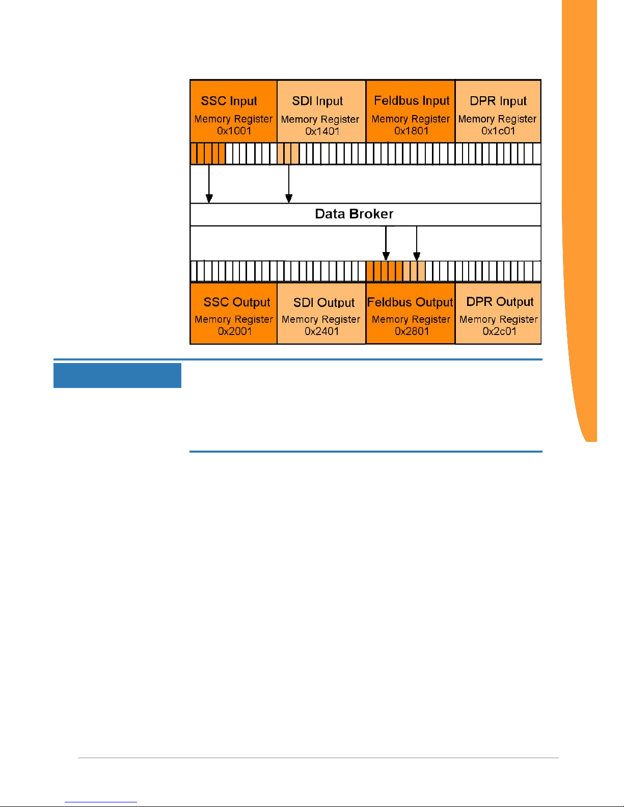
Example of a Mapping
The following example explains, step-by-step, how to map the first
three SDI input registers and the first five SSC input registers to the
field output register.
If you would like to participate in this example, you will need a
functional CDI connection. Section "Setting up a Serial Connection
[}93]" explains how this works.
Input options in the CDI menu:
You can enter hexadecimal (with prefixed 0x) or decimal numbers in
the CDI menu.
[Esc] Go back one level
[Enter] Confirm input/selection
[b] Value is displayed in binary code
[h] Value is displayed in hexadecimal
code
[d] Value is displayed in decimal
code
Components
Page 25

KUNBUS-COM EtherCAT 25 / 135
◦ Open the main menu of the CDI as described in the Appendix "Setting
up a serial connection using PuTTY".
Main Menu
The main menu is your access point for operating the module using
the CDI. After a reset, the module transmits this main menu to the
terminal.
-------------------------------------------------KUNBUS-COM – Main Menu
-------------------------------------------------1 – Module Information
2 – Interface Configuration
3 - Monitor Communication
4 – Module Status
------------------------------------------------->
Configuration menu
◦ In the main menu enter [2]+[Return].
ð You will be taken to the configuration menu "2-Interface Configuration"
In this menu you have the option to set the mapping for the data
broker and the operational parameters for the different interfaces.
– Select "Fieldbus Output Mapping" to define the data source for the
fieldbus output register.
-------------------------------------------------KUNBUS-COM – Interface Configuration
-------------------------------------------------Operating Mode: Config
1 - SDI Communication
2 - CDI Communication
3 - SSC Communication
4 - DPR Configuration
6 - SDI Output mapping
7 - SSC Output mapping
8 - Fieldbus Output mapping
9 - DPR Output mapping
11 - Fieldbus Specific
12 - Set Arbitrary Register
13 - Script Interpreter
14 - Reset Module
15 - Reset to Factory Settings
16 - Extended Mapping
------------------------------------------------->
Components
Page 26

KUNBUS-COM EtherCAT
26 / 135
– With the selection 1-8 are 8 positions available to create a mapping.
-------------------------------------------------KUNBUS-COM - Fieldbus Outputmapping
-------------------------------------------------Src Register Number
1 - 1 (0x0001) | 0
2 - 1 (0x0001) | 0
3 - 1 (0x0001) | 0
4 - 1 (0x0001) | 0
5 - 1 (0x0001) | 0
6 - 1 (0x0001) | 0
7 - 1 (0x0001) | 0
8 - 1 (0x0001) | 0
9 - Default Data: all zero
10 - Valid Time: disabled
------------------------------------------------->
◦ Enter [1] + [Return].
◦ Specify the first 3 registers of the SDI input register as data source
(start address 0x1401).
◦ Confirm your entry with [Return]
ð After confirming, you will return automatically to the "Fieldbus Output
Mapping" menu
You can find an overview of the start addresses in the section
"Overview of the Memory Register [}47]".
-------------------------------------------------KUNBUS-COM – Edit one map entry
-------------------------------------------------Source Register: 0x1401
Number of Registers: 3
◦ Create another mapping at the next free position
◦ Select the first 5 registers of the SSC input register as data source (start
address 0x1001)
-------------------------------------------------KUNBUS-COM – Edit one map entry
-------------------------------------------------Source Register: 0x1001
Number of Registers: 5
Components
Page 27

KUNBUS-COM EtherCAT 27 / 135
In the menu for fieldbus outputmapping, you can see the finished
mapping.
-------------------------------------------------KUNBUS-COM - Fieldbus Outputmapping
-------------------------------------------------Src Register Number
1 - 1521 (0x1401) | 3
2 - 4097 (0x1001) | 5
3 - 1 (0x0001) | 0
4 - 1 (0x0001) | 0
5 - 1 (0x0001) | 0
6 - 1 (0x0001) | 0
7 - 1 (0x0001) | 0
8 - 1 (0x0001) | 0
9 - Default Data: all zero
10 - Valid Time: disabled
------------------------------------------------->
The new mapping becomes active after a restart of the module. To
perform a restart, you have the following options:
1. Switch the module off and on again.
2. [Esc] takes you to the CDI menu [2] "Interface Configuration".
Here, enter [14] + [Return].
In CDI menu [2] "Interface Configuration" under menu item
"Set Arbitrary Register" you now have the option to write the
values in the SDI-In data area. The registers 0x1401 - 0x1500 are
available to you for this purpose.
In menu [3] "Monitor Communication", under menu item "
Arbitrary Register" you can view the fieldbus output register
from address 0x2801.
NOTICE
Fault due to fine settings
Some settings lead to malfunctioning of the module.
If you already want to test some settings now, read section CDI Menus
[}96]CDI Menus.
Also see about this
2 [}75]
2 Register for the Mapping [}75]
2 Setting up a Serial Connection [}93]
Components
Page 28

KUNBUS-COM EtherCAT
28 / 135
4.4 Fieldbus Interface
The fieldbus interface connects the Modul to EtherCAT.
It also enables access to the fieldbus specific Memory Register.
You can find the overview of the available Modbus registers in the
section "Overview of the Memory Register".
Also see about this
2 Overview of the Memory Register [}47]
2 Overview of the Memory Register [}47]
4.5 CDI - Configuration and Debug Interface
At the application interface, serial cables are available (RS232
interface with 3.3 V logic levels). You can connect these cables to a
terminal or PC with terminal simulation (e.g. PuTTY) using an
interface IC on the main board (see the application sample circuit
diagram, Appendix 2). You can read and change parameters using
structured menus. The CDI is also used for downloading scripts and
firmware updates.
The CDI is suitable for configuration during the development and for
diagnostic purposes. To configure several modules automatically, we
recommend performing the settings with "Modpoll". "Modpoll" is
freely-available software. You can find an introduction and example
of this in the Appendix Configuration via Modpoll [}134].
The serial interface is located at the application interface. The
respective cables are provided there with 3.3V logic levels. To
connect these cables, you have the following options:
– Connect the cables directly with the UART inputs of the microprocessor
on the main board
– Convert the cables to standardised levels using level converters or
interface ICs. Afterwards, place the converted levels onto connectors for
connecting a PC or terminal.
We deliver the Modul to you with the following default settings to
enable access via the CDI :
• 115200 bit/s
• 8 data bits
• 1 stop bit
• Even parity (Even)
In section CDI Menus [}96], we have compiled a detailed
description of the menus for you.
Components
Page 29

KUNBUS-COM EtherCAT 29 / 135
4.6 DPR - Dual Port RAM
-The COMS-Modul contains a special memory module (RAM with 1
Kbyte length), whose memory addresses the processor of the
module can also access, like an external processor, which is
connected to the module via the DPR interface.
If the application where the COMS-Modul is used should exchange
extensive data quickly, then this type of communication between the
base board and COMS-Modul is ideal. This absolutely requires the
use of a microprocessor on the base board, however, which operates
the DPR interface.
Many pins of the application interface are required for this parallel
access to the DPR. This results in a different PIN assignment in the
DPR mode of the module (this is switched on and off via the logic
level on PIN a14). In parallel access mode, no SSC or SDI interfaces
are available.
The data exchange between application circuitry and the COMSModul via DPR can take place in two different ways:
– Process data is read in and read out cyclically from the Data Broker via
two fixed address ranges for input and output data. In this case, the
DPR reacts like another communication interface, as a producer and
consumer. The data is distributed according to the specifications set in
the Data Broker.
– Messages are exchanged via two address ranges for an input and
output "mailbox" by means of defined handshaking. The messages
include:
– Commands for writing and reading the memory registers
– Addresses of the memory registers
– Data lengths
– Register contents to be written or read
This communication via mailboxes replaces the Modbus
communication via SDI in parallel access mode (which is not
available in this mode). All parameters in parallel access mode can
only be read or written via CDI interface or DPR mailboxes.
To enable these two types of communication, the 1Kbyte
memory of the DualPortRAM interface is subdivided into five
areas:
Dual Port RAM
Configuration Incoming
mailbox
Outgoing
mailbox
Process data
input
Process data
output
Components
Page 30

KUNBUS-COM EtherCAT
30 / 135
The size of the individual areas can be adapted to the respective
application and is saved non-volatile in parameter registers. The
configuration area has a fixed length and provides the necessary
address offsets as well as handshaking data for external access to
the remaining areas.
We recommend using our Evaluation Board and the C source files
provided with this as a template for developing the application side of
a DPR interface. Upon request, we can also provide you with the
documents and source codes of the Evaluation Board separately.
Therefore, in this section we will only describe the basic procedure
when using the DPR interface.
Each mailbox controls and coordinates the data transmission
individually during communication by means of corresponding control
values, length specifications and error codes in the relevant headers
of the data packets. The process data of memory areas also
coordinates the exchange of data between the base board and
COMS module by means of a corresponding data header.
NOTICE
Important instructions on using the DPR
èYou can operate the KUNBUS-COMS module either in DPR mode or in
SPI/SSC mode.
ð You determine the mode by setting the logic level on PIN a14 (+3.3
V = 1 = SPI/SSC mode, GND = 0 = DPR mode). you will find
information about the current interface mode in the CDI menu: "4 Module Status > 1 - Common Status"
èIf you use the Scripter [}44] in DPR mode, you must bear in mind that
the scripter can only communicate via the CDI.
ð Changes to parameter registers are then still only possible via the
DPR mailboxes.
Components
Page 31

KUNBUS-COM EtherCAT 31 / 135
4.7 SDI - Serial Data Interface
The serial data interface allows the application to access the
individual Memory Register via the Modbus-RTU protocol. This
allows you to configure the COMS-Modul automatically and to write
productive data in the input registers or to read it from the output
registers.
The serial data interface is located at the application interface. The
respective cables are provided there with 3.3V logic levels. To
connect these cables, you have the following options:
– Connect the cables directly with the UART inputs of the microprocessor
on the main board
– Convert the cables to standardised levels using level converters or
interface ICs. Afterwards, place the converted levels onto connectors for
connecting a PC or terminal.
We deliver the Modul to you with the following default settings to
enable access via the SDI :
• automatic baudrate detection
• 8 data bits
• 1 stop bit
• Even parity (Even)
Automatic bitrate detection means that the module tests the following
bitrates until it has received a correct Modbus-RTU telegram:
• 2400 bit/s
• 4800 bit/s
• 9600 bit/s
• 19200 bit/s
• 38400 bit/s
• 57600 bit/s
• 115200 bit/s
NOTICE!During automatic bitrate detection the module does not
send a reply to the master until the correct bitrate has been
detected. This procedure can require up to 40 polls of the
master.
TIP: Set a fixed bitrate if the automatic bitrate detection lasts too
long for you.
You can make the settings optionally using theCDI [}96] or in
thememory register 0x0005 [}54].
Components
Page 32

KUNBUS-COM EtherCAT
32 / 135
4.8 Synchronous serial interface
A synchronous serial interface is available to you on the application
interface. To use this interface, you have to set the logical level of pin
a14 to high (3.3V).
The synchronous serial interface can be used in 2 operating modes.
Select the operating mode you require via the logical level on pin a6:
– 0 (GND) = SPI Slave for connecting to an SPI Master
– 1 (3.3V) = SSC Master for connecting to a shift register chain
The following pins are available for operating as an SPI Slave for
connecting to an SPI Master:
– a4 SPI Clock (input)
– a5 SPI Data in (MOSI, input)
– b4 SPI Data out (MISO, output)
– b5 SPI Chip Select (CS, input)
– b6 SPI ready (output)
The following pins are available for operating as an SSC Master for
connecting to a shift register chain:
– a4 SSC Clock (output)
– a5 SSC Data out (MOSI, output)
– a7 SSC centre tap (MID, input)
– b4 SSC Data in (MISO, input)
– b6 SSC Strobe Signal (LOAD, output)
– b7 SSC Reset (output)
Output data from the Data Broker is written to the SSC output
register area and input data is read from the SSC input register area
in both operating modes. The SPI Slave operating mode also allows
an SPI Master write and read access to all other Memory Register
that are enabled for this. This section describes how this functions in
detail.
Operating mode as SPI Slave
In SPI Slave mode, the transmission of the process data between an
SPI Master and the SSC Input or Output registers takes place in data
blocks, which, in addition to the actual process data, also contain
metadata (e.g. for indicating the register addresses for source and
target areas). Such data blocks are transmitted with a hardware
handshake. The actual data transmission lines MOSI, MISO and
Clock are used with 3.3 V logic in the usual manner, as described
below in the document S12SPIV4 "SPI Block Guide" von Motorola /
Freescale®. Here, you can freely select the normally alterable
Components
Page 33

KUNBUS-COM EtherCAT 33 / 135
parameters CPOL (Clock polarity) and CPHA (Clock Phase) in
COMS-Modul and define these permanently via the CDI Menu
[}102] or memory register [}60]. The bit sequence (MSB first or
MSB last) is fixed for COMS modules, the module always starts the
transmission with the MSB (bit of highest value) of a byte. All bytes
belonging to a block are transmitted in a continuous sequence. The
clock signal required is input to PIN a4 externally from the Master.
The COMS-Modul can process maximum clock frequencies of
20MHz.
Handshaking
The handshaking lines ensure that a Master first sends the
subsequent transmission block after the module has processed the
block that was received previously.
The module indicates by the "low" level on the SPI ready line that a
transmission cycle has been completed, the status of the last
transmission is waiting to be retrieved and the Master can trigger the
next cycle. The Master starts this cycle by setting the SSC Chip
Select line to "high" to indicate to the module that data is ready for
transmission and the following data block is meant for the module
(theoretically, a master can address several modules). Once the
module is now ready for this data transmission, it sets the SPI ready
line to "high" and the Master can start transmission of the block
immediately. A maximum delay between setting the CS signal and
releasing by the ready signal of the module is 10ms. All bytes of a
data block are now transmitted directly in succession at the rate
preset by the Master. After the last bit of the data block has been
transmitted, the Master indicates the end of the transmission by
resetting the SPI Chip Select line to "low". The module responds to
this by resetting the SPI Ready line to "low". This happens at the
earliest, however (maximum 10 ms after resetting CS), when the
data has been processed insofar as the status was determined and
is ready in the SPI output buffer so that the next transmission can
start. This must first be requested, however, by the Master (as
described above) by setting the SPI Chip Select line to "high".
Chip Select
(Master)
Ready
(Slave)
Data
(Master & Slave)
Components
Page 34

KUNBUS-COM EtherCAT
34 / 135
Protocol
KUNBUS has defined a separate protocol for the data exchange via
the synchronous serial interface. This protocol allows you to perform
various read and write access operations. Here, the Master first
always sends a transmission block with at least 5 bytes. The first 3 to
5 bytes of this transmission block consist of meta data (target
address, etc.). Depending on the access type, another transmission
block of variable data length follows the first block. Write and read
access to the memory register of the module is performed. Only
memory registers that have been enabled can be written or read, of
course. The following areas cannot be written:
Input data areas:
– Fieldbus
– SDI
– DPR
Output data areas:
– Fieldbus
– SSC
– SDI
– DPR
When writing to the SSC input data area, the time monitoring is reset
for this area (see Valid Time, Section "Data Broker [}20]").
Read access to the DPR areas is fundamentally not possible. The
module can never be in SPI/SSC mode and DPR mode at the same
time. Consequently, access to DPR areas would make no sense.
The various access types are explained below.
Writing 1 byte
This access type is used if 1 byte is written to a memory register of
the module by the Master.
The Master first sends a transmission block with a fixed length of 5
bytes, which have the following content:
Transmission block with fixed length
Command
code
(1 byte)
Address area
(2 bytes)
Data area
(1 byte)
Mask area
(1 byte)
Description
0x01 0x0000-0xFFFF 0x00-0xFF 0x00-0xFF WRITE_LOW_BYTE
0x02 0x0000-0xFFFF 0x00-0xFF 0x00-0xFF WRITE_HIGH_BYTE
0x00 0xXXXX 0xXX 0xXX NO_OPERATION*
Theoretically, you could use all memory register addresses between
0 and 0xFFFF. In practice, however, the write access is limited to
registers that are enabled for this purpose. The byte can be written to
the high or low byte position of the 16-bit wide register by selecting
Components
Page 35

KUNBUS-COM EtherCAT 35 / 135
the associated command code. The mask byte only makes it
possible to write single bits to the target register. Thereby, only bits
that are set to "1" in the mask are transferred from the data byte (i.e.
these bits are set to the value as found in the data byte). All other bits
are left unchanged in the register.
During transmission of this first block, the module sends the status of
the previous data transmission. The module first returns the status
for the previous access when sending the next transmission block. If,
however, no further write or read operation should follow the write
access, then the Master must send another transmission block with
the command code 0 ("NO_OPERATION") for retrieving the status,
in which the module returns the status for the last write access
operation.
The status response from the module is structured as follows for all
write access types:
Transmission block with fixed length
Status code
(1 byte)
Error code
(2 bytes)
Not used
(2 bytes)
Description
0x00 0xXXXX 0xXXXX NO_PREVIOUS_OPERATION
0x01 0x0000 0xXXXX WRITE_SUCCESS
0x02 ERROR_CODE
1
0xXXXX WRITE_FAILURE
1
See Table "ErrorCode"
The first byte returns the status. If it is set to "0", the Master then
indicates that it cannot return any current status information since
there was no previous operation (this is usually the response to the
very first block transmission). A "1" indicates the successful
completion of the previous transmission. In the case of a 2, the
module sends the error code of an error in the subsequent byte,
which occurred during the previous block transmission. The possible
error codes are listed at the end of this subsection.
Writing 2 bytes (Word)
This access type basically proceeds as when writing 1 byte. It differs
in the following points:
– Instead of a mask byte, the second byte of the 16-bit wide user data is
transmitted with the data block. Access to individual bits in the target
register is not possible with this access type.
– The 16-bit wide register content to be written must be prepared by the
Master in such a way that the higher-value byte is transmitted as the 4th
byte and the lower-value byte is transmitted as the 5th byte ("BigEndian" or "Motorola format").
Components
Page 36

KUNBUS-COM EtherCAT
36 / 135
Transmission block with fixed length
Command
code
(1 byte)
Address area
(2 bytes)
Data area
(2 byte)
Description
0x04 0x0000-0xFFFF 0x0000-0xFFFF WRITE_WORD
0x00 0xXXXX 0xXXXX NO_OPERATION*
The status response has the same structure and meaning as write
access with 1 byte
Writing more than 2 bytes
with one access (bulk-write)
This access type is suitable for larger volumes of data. The number
of target registers to be written and start address are transmitted with
the first transmission block. As with the previous access types, the
first transmission block also has a fixed length of 5 bytes here. After
this block with metadata, the user data follows in a separate
transmission block with variable length. The maximum permitted
number of target registers to be written depends on the target area: A
maximum of 128 registers (each 16-bit = 1 word) are permitted for
writing to the SSC input register area. A maximum of 16 registers per
block is to be written for all other target areas.
All 16-bit wide register contents to be written must be prepared by
the Master in such a way that the higher-value byte is transmitted as
the first byte and the lower-value byte is transmitted as the second
byte ("Big-Endian" or "Motorola format"). The register contents must
be sent in ascending address order, i.e. the start address first.
Transmission block with fixed length
Command
code
(1 byte)
Address area
(2 bytes)
Data length
(2 bytes)
Description
0x08 0x0000-0xFFFF 1-16/128 WRITE_BULK
0x00 0xXXXX 0xXXXX NO_OPERATION*
NOTICE
The maximum data length for writing in the SSC input data area is 128
registers (256 bytes).
If this value is exceeded, errors in the data communication will result.
In the case of a transmission block of variable length, the module
sends bytes with the value 0 to the master.
The status response has almost the same structure and meaning as
write access with 1 byte. In the event of an error, a 16-bit wide
register address is at position 4 and 5 for this transmission type, at
which the first error occurred. The status is transmitted in the first
transmission block that follows the data block with variable length.
Components
Page 37

KUNBUS-COM EtherCAT 37 / 135
Transmission block with fixed length
Status code
(1 byte)
Error code
(2 bytes)
Address area**
(2 bytes)
Description
0x00 0xXXXX 0xXXXX NO_PREVIOUS_OPERATION
0x01 0x0000 0xXXXX WRITE_SUCCESS
0x02 ERROR_CODE10x0000-0xFFFF WRITE_FAILURE
1
See Table "ErrorCode"
** Address where an error occurs
Reading 2 bytes (Word)
This access type is used if just 1 register is to be read from a
memory register of the module by the Master. The Master first sends
a data block with a fixed length of 5 bytes, which have the following
content:
Transmission block with fixed length
Command
code
(1 byte)
Address area
(2 bytes)
Not
used
(2 bytes)
Description
0x10 0x0000-0xFFFF 0xXXXX READ_WORD
0x00 0xXXXX 0xXXXX NO_OPERATION*
* This command allows the master to request the status of a read
request without an additional read or write request having to be
executed.
Theoretically, you could use all memory register addresses between
0 and 0xFFFF. In practice, however, the write access is limited to
registers that are enabled for this purpose.
During transmission of the first data block, the module sends the
status of the previous data transmission. The module first returns the
data to be read when sending the next data block. If, however, no
further write or read operation should follow the read access, then
the Master must send another data block with the command code 0
("NO_OPERATION") for retrieving the data to be read, in which the
module returns the status for the last write access operation.
The response from the module is structured as follows for all read
access operations:
Transmission block with fixed length
Status code
(1 byte)
Error code
(2 bytes)
Data area
(2 byte)
Description
0x00 0xXXXX 0xXXXX NO_PREVIOUS_OPERATION
0x01 0x0000 0x0000-0xFFFF READ_SUCCESS
0x02 ERROR_CODE10xXXXX READ_FAILURE
1
See Table "ErrorCode"
Components
Page 38

KUNBUS-COM EtherCAT
38 / 135
The first byte returns the status. If it is set to "0", the Master then
indicates that it cannot return any current status information since
there was no previous operation (this is usually the response to the
very first block transmission). A "1" indicates the successful
completion of the previous transmission. In the case of a 2, the
module sends the error code of an error in the subsequent byte,
which occurred during the previous block transmission.
If the status is "1", the 2 bytes after that at position 4 and 5 contain
the content of the memory register to be read at the address that was
transmitted at the last block with the read command. The 16-bit wide
register content read is prepared by the module in such a way that
the higher-value byte is transmitted as the 4th byte and the lowervalue byte is transmitted as the 5th byte ("Big-Endian" or "Motorola
format").
In the case of status "0" or "2", both data bytes at position 4 and 5
are invalid and must be discarded by the Master.
Reading more than 2 bytes
(Bulk-Read)
In this access type, the number of source registers to be read as well
as the start address are transmitted with the first transmission block
that has a fixed length of 5 bytes. After this block with metadata, the
transmission of the read data follows in a separate transmission
block with variable length. Therefore, this access type is suitable
primarily for larger volumes of data. The maximum permitted number
of source registers to be read depends on the source area: A
maximum of 128 registers (each 16-bit = 1 word) are permitted for
reading from the SSC output register area. A maximum of 16
registers per block is to be read for all other source areas. Byte
order:
All 16-bit wide register contents read are prepared by the module in
such a way that the higher-value byte is transmitted as the first byte
and the lower-value byte is transmitted as the second byte ("BigEndian" or "Motorola format"). The register contents are sent in
ascending address order, i.e. the start address first.
Transmission block with fixed length
Command
code
(1 byte)
Address area
(2 bytes)
Data length
(2 bytes)
Description
0x20 0x0000-0xFFFF 1-16/128/256 READ_BULK
0x00 0xXXXX 0xXXXX NO_OPERATION*
The Master sends a block of variable length with 0 bytes to the
module.
Components
Page 39

KUNBUS-COM EtherCAT 39 / 135
The status response has almost the same structure and meaning as
read access with 1 byte. In the event of an error, a 16-bit wide
register address is at position 4 and 5 for this transmission type, at
which the first error occurred. The status is transmitted in the first
transmission block that follows the data block with variable length.
In the event of an error during bulk access (status "2"), the data
transmitted by the module from the data block with variable length is
invalid and must be discarded by the Master.
Transmission block with fixed length
Status code
(1 byte)
Error code
(2 bytes)
Address area
(2 bytes)
Description
0x00 0xXXXX 0xXXXX NO_PREVIOUS_OPERATION
0x01 0x0000 0xXXXX READ_SUCCESS
0x02 ERROR_CODE10x0000-0xFFFF READ_FAILURE
1
See Table “ Error code“
** Address where an error occurs
Transmission block with variable length (1-16/128 words)
Data area
0x0000-0xFFFF"
Simultaneous reading and
writing of more than 2 bytes
with one access (bulk read/
write)
In this access type, the number of source registers to be read or
target registers to be written are transmitted with the first
transmission block that has a fixed length of 5 bytes. After this block
with metadata, the transmission of the read data follows in a
separate transmission block with variable length. Unlike with BulkRead or Bulk-Write, no random start address can be defined for this
access type. The start address for the block to be read is preset with
0x2001 (SSC input register) and with 0x1001 (SSC output register)
for the block to be written. Byte order:
All 16-bit wide register contents to be read or written are prepared by
the module in such a way that the higher-value byte is transmitted as
the first byte and the lower-value byte is transmitted as the second
byte ("Big-Endian" or "Motorola format"). The register contents are
sent in ascending address order, i.e. the start address first.
Transmission block with fixed length
Command code
(1 byte)
Not
used
(2 bytes)
Data length
(2 bytes)
Description
0x40 0xXXXX 1-128 READ_WRITE_BULK
0x00 0xXXXX 0xXXXX NO_OPERATION*
Components
Page 40

KUNBUS-COM EtherCAT
40 / 135
Transmission block with variable length (1-16/128 words)
Data area
0x0000-0xFFFF"
The status response has almost the same structure and meaning as
read access with 1 byte. In the event of an error, a 16-bit wide
register address is at position 4 and 5 for this transmission type, at
which the first error occurred when reading or writing. The status is
transmitted in the first transmission block that follows the data block
with variable length.
Transmission block with fixed length
Status code
(1 byte)
Error code
(2 bytes)
Not used
(2 bytes)
Description
0x00 0xXXXX 0xXXXX NO_PREVIOUS_OPERATION
0x10 0x0000 0xXXXX READ_WRITE_SUCCESS
0x20 ERROR_CODE10xXXXX READ_WRITE_FAILURE
In the event of an error during bulk access (status "2"), the data
transmitted by the module from the data block with variable length is
invalid and must be discarded by the Master.
Error Codes
Error code Designation Description
0x01 INVALID_DATA_
ADDRESS
Invalid data address
The master tries to access an invalid address.
The slave ignores the instruction.
0x02 INVALID_DATA_
LENGTH
Invalid data length
The data length predefined by the master is
too great.
The slave ignores the instruction.
0x04 INVALID_DATA Invalid data
The master tries to write data containing
values outside a valid range.
The slave ignores the instruction.
0x08 INVALID_ACCESS Invalid access
The master tries to access an invalid area
or a valid address.
The slave ignores the instruction.
0x10 INVALID_RANGE Invalid range
The master tries to write beyond the limits
of an SSC input data area or to write beyond the limits of an SSC, SDI, FBS or DPR
output data area.
The slave ignores the instruction.
0x20 UNDEFINED_ERROR Undefined error
An undefined error has occurred.
The slave ignores the instruction.
Table1: Error Code
Components
Page 41

KUNBUS-COM EtherCAT 41 / 135
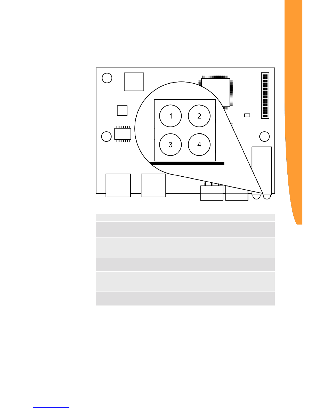
SSC Master Operating Mode
In this operating mode, output data is read from the SSC output
register area via the serial synchronous interface and input data is
written to the SSC input register area. This takes place via a
hardware shift register chain.
Illustration11: Hardware shift register chain, example with 4 inputs and outputs
The advantage of such an interface is the possibility of forwarding
input and output signals to the fieldbus without the need of
microprocessor controlled application circuitry. Switches, contacts,
relay coils or solenoid valves, for example, can therefore be
connected directly via EtherCAT without using a microprocessor.
The COMS-Modul with its clock (Pin a4) clocks the output data into
the input register of the chain via the MOSI line (Pin a5), where it is
shifted bit by bit until the end. At the same time, the input data is
shifted bit by bit via the MISO line into the COMS-Modul with the
same clock pulse. Prior to each such shift procedure, the module
sets the LOAD line to high (Pin b6). In this way, the parallel outputs
Components
Page 42

KUNBUS-COM EtherCAT
42 / 135
of all shift register modules receive the data from the input buffers in
the previous cycle. The input shift registers, on the other hand, utilise
the positive edges from the LOAD signal to copy all parallel input
values simultaneously to their output buffers. From there, they are
shifted bit by bit to the SSC input register area of the COMSModulduring the current cycle.
The clock rates of the COMS-Moduls can be adapted manually or
automatically in 3 levels and are about 300, 1200 or 4800 Kbit/s. The
load impulse is between 5 and 15 µs long (active low). The delay
between the load edge (positive edge of the load impulse) and the
first clock edge (from high to low) is between 1 and 2 µs. These
values are completely uncritical when using the shift register modules
74HC165 (Input) and 74HC594 (Output).
An optional RESET line (Pin b7, active low) initialises the shift
register modules during the starting process of the COMS-Moduls
(i.e. also during each reset of the module).
With an arrangement of the output and input shift register as shown
in this example, all registers are switched in series so that the
COMS-Modulhas its own output data shifted back into the input
register again for checking purposes. A test sample shifted through
the complete chain without a LOAD signal allows the COMS-Modulto
detect how long the entire chain is by means of the necessary clock
signals for such a shifting procedure. A centre pickoff between the
output and input modules allows the COMS-Modul to also detect the
corresponding number of inputs and outputs during this run of a test
sample. If bit errors occur, the clock rate is reduced in automatic
mode by one level. Hence, with such a structure the COMSModulcan find the right setting for the chain lengths and maximum
possible transmission rate independently. It is also possible,
however, to assign the lengths and clock rates manually via the CDI
menu. In this case, the centre pickoff can also be omitted (it is only
needed for determining the allocation between outputs and inputs).
The entire chain length is monitored constantly during ongoing
operation and must match the configured length. If the module
detects a difference, then it shuts down the SSC communication and
reports an error status via its status register.
The COMS-Modulcan operate a maximum of 32 input shift registers
plus 32 output shift registers. These limits must be observed.
Note on cycle time: The cycle time of the shift register interface is
normally independent of its chain length since theCOMS-Modulin its
work cycle only starts the transmission of a shift procedure. The shift
Components
Page 43

KUNBUS-COM EtherCAT 43 / 135
procedure itself then takes place independently of the work cycle of
the COMS-Moduls. Its length is determined by the number of cycles
as well as the clock rate. After completion of a shift procedure, the
next shift cycle starts with the next work cycle of the module. The
maximum delay between the completion and start of a shift cycle is
10ms.
Note ! If the shift procedure is longer than a work cycle of the
module, the cycle time is determined by the length and speed of the
shift register chain.
Components
Page 44

KUNBUS-COM EtherCAT
44 / 135
4.9 Scripter
The COMS-Modul includes a software component that allows you to
set up customer-specific data exchange protocols for SDI or CDI
serial interfaces. If, for example, the module is to communicate in an
application with a serial-controlled servomotor, this servomotor
expects a preset protocol to be processed in order to receive the
actuator values or to return sensor values. With the aid of the
Scripter you can load small executable program sequences into the
module that are then executed there cyclically. With the appropriate
data exchange protocol the module can receive such actuator values
e.g. via EtherCAT and transmit these via the serial interface of the
module (SDI or CDI) to the servomotor. The program sequences
required are loaded once into the module in the form of a script via
the CDI interface of the module and then always executed there
cyclically. KUNBUS provides you with a PC tool for creating and
testing such scripts. You can read all the necessary details in the
separate manual on the Scripter.
NOTICE!Please note that when using the Scripter and activating
a script the interface (CDI or SDI) selected for its communication
is always assigned for the Scripter. If you choose the CDI interface,
you can then no longer use this interface to check and enter module
parameters ("CDI menus" are then no longer available). If you
choose the SDI interface as a serial communication channel for the
Scripter, you can then no longer process any Modbus protocol with
access to the memory register via this interface.
As a reminder: The SDI interface is no longer available when the
module works in DPR mode.
Components
Page 45

KUNBUS-COM EtherCAT 45 / 135
5 Commissioning
5.1 Installation
To connect the module directly to the control board, proceed as
follows:
ü Attach suitable spacer bolts on the control board. Each module has
three identical holes for spacer bolts. These bolts stabilise the module
with a direct connection onto the control board.
◦ Fasten the module "head first" to the application contact strip of the
control board. The spacer bolts must be on the corresponding holes in
the board and the module kept parallel at a distance to the control
board.
◦ Fasten the module by screwing down the spacer bolts to the module
board
ð You have successfully integrated your application and can now
configure it.
Also see about this
2 Spacer bolt [}9]
Commissioning
Page 46

KUNBUS-COM EtherCAT
46 / 135
5.2 Configuration
This section describes how to configure the module and associated
components and applications.
NOTICE
Ø The module has no undo function.
èChanges are applied after a reset or start of the operating mode without
any further confirmation.
ð If you want to reset all values, use the function "Reset to factory
settings". [}116] Please note that all previous settings made will be lost.
Configuration using the CDI
To configure the Modul and put it into operation using the CDI, you
need a PC or notebook with a serial interface (RS-232) or USB/serial
adapter. Make sure that the adapter drivers are installed.
Communication with the CDI (Configuration and Debug Interface) of
the module takes place using a terminal program (e.g. PuTTY for
Microsoft Windows®).
TIPP!: Das CDI is suitable for configuration during the development
and for diagnostic purposes. To configure several modules
automatically, we recommend performing the settings with Modpoll.
You can find an introduction and example of this in the Appendix
Configuration via Modpoll [}134].
Configuration using the SDI
The COMS-Modul has a UART interface with 3.3 V logic levels. Your
main board must convert these lines to standardised RS-485 signals
so that Modbus/RTU devices can access these. Conversion to
standardised RS-232 signals is generally necessary for
communication with a PC. The base board of the evaluation board
has both interfaces that can each be selected via jumpers.
Configuration using the SDI requires a Modbus master device.
One of the following devices is suitable for this:
– Master computer,
– Control panel,
– Programming device,
– SPS with the possibility of Modbus-RTU communication.
To communicate with the SDI of the module using a PC, you need
Modbus software (e.g. Modpoll).
5.3 Firmware Update
If a firmware update is required, please contact our support
(support@kunbus.de). We will be delighted to provide you with all the
information you need for your product.
Commissioning
Page 47

KUNBUS-COM EtherCAT 47 / 135
6 Memory Register
6.1 Overview of the Memory Register
The storage unit is the central component for all functions of the
COMS-Module. It is subdivided into individual Memory Register with
a width of 16 bits each. In these Memory registers the following
information is stored:
– Input and output data
– Configuration settings
– Module Status
– Error states
The functionality of the addressing was incorporated from Modbus.
The register assignment depends on the application and is not
specified by the Modbus specification. A Memory Register according
to this specification has a register number between 1 (0x0001) and a
maximum of 65536 (0x10000), of which the module only uses a small
part, however.
With 8-bit values, 1 byte remains unused. 32-bit values are stored in
2 registers.
The 16-bit values are stored internally in the memory in Little Endian
order. This must be taken into account when you access data via the
fieldbus interface, SDI or SSC.
NOTICE!In the description of the individual memory registers
and CDI, the memory registers are also referred to as Modbus
registers.
Memory Register
Page 48

KUNBUS-COM EtherCAT
48 / 135
Bitwise access to input and
output data
Optionally, you can address input and output data areas bitwise. The
functions 01 Read Coil Status, 02 Read Input Status and 05 Force
Single Coil are defined in Modbus for this purpose. Since each bit
has a separate address, they are assigned to the bits in the registers
as follows: Coil 0x0001 corresponds to the lowest value bit 0 of
register 0x0001, Coil 0x0002 corresponds to bit 1, etc. coil 0x11 is
the bit 0 from register 0x0001 etc.
The table below shows the start addresses of the data areas:
Area Memory Register Coil/Input Address
Input SSC 0x1001 - 0x1080 0x0001 – 0x0800
Input SDI 0x1401 – 0x1500 0x2001 – 0x4000
Input FBS 0x1801 - 0x1880 0x4001 – 0x6001
Input DPR 0x1c01 … 0x6001 …
Output SSC 0x2001 – 0x2080 0x8001 – 0x8800
Output SDI 0x2401 – 0x2500 0xa001 – 0xb000
Output FBS 0x2801 - 0x2880 0xc001 – 0xe001
Output DPR 0x2c01 … 0xe001 …
Register assignment of the memory area
The following table contains a brief overview of the register
assignment of the general memory area. You can find a detailed
overview of the individual registers on the following pages.
Register number Assignment Description
0x0001 – 0x0100
[}50]
General Device
Parameters
e.g. Setting of the bitrates,
mailbox sizes etc.
0x0101 – 0x0e00 Reserved 0x0e01 – 0x0ea0
[}75]
Register for mapping
the output data
Each channel occupies
2 x 8 registers
0x0f01 – 0x0xf40
[}76]
Register for mapping of
the extended Data
Broker
16 mappings occupy
4 registers each
0x1001 – 0x2000
[}78]
Input memory of the
communication
channels
Each communication channel
has a preallocated memory
area of 128 - 256 registers.
0x2001 – 0x3000
[}79]
Output memory of the
communication
channels
Each communication channel
has a preallocated memory
area of 128 - 256 registers.
0x3001 – 0x4000 Reserved 0x4001 – 0x5000 Fieldbus-specific
(s. following table)
See the description of the
individual fieldbus variants
0x5001 – 0x10000 Reserved -
Memory Register
Page 49

KUNBUS-COM EtherCAT 49 / 135
The following table contains a brief overview of the register
assignment of the memory area for EtherCAT. You can find a
detailed overview of the individual registers on the following pages.
Register Designation Register Designation
0x4001 [}81]
Fieldbus Status
0x4002 [}81]
Module Status
0x4003 [}82]
Manufacturer ID,
High Byte
0x4004 [}82]
Manufacturer ID,
Low Byte
0x4007 [}82]
Fieldbus Version,
High Byte
0x4008 [}82]
Fieldbus Version,
Low Byte
0x4009 [}82]
Firmware Version
0x400a [}83]
Serial number,
High Byte
0x400b [}83]
Serial number,
Low Byte
0x400c [}83]
Physical Address
0x400f [}84]
Available Ports
0x4011 [}84]
Configuration
Bits, High Byte
0x4012 [}84]
Configuration
Bits, Low Byte
0x4014 [}86]
Product number,
High Byte
0x4015 [}86]
Product Number,
Low Byte
0x4016-0x4035 Product Name
0x4036 [}86]
Fieldbus Input
Size
0x4037 [}87]
Fieldbus Output
Size
0x4100 [}87]
Station Alias
Configured
0x4101 [}87]
Current Station
Alias
0x4103 [}87]
Station Alias from
SSC
0x4104 [}88]
Explicit Device ID
Configured
0x4105 [}88]
Current Explicit
Device ID
0x4106 [}88]
Explicit Device ID
from SSC
Memory Register
Page 50

KUNBUS-COM EtherCAT
50 / 135
6.2 General Device Parameters
0x0001 Set operating mode
In this memory register you have the option, the operating mode to
set
Modbus Register 0x0001
Value Range 0x0000-0x0003
Default Value 0x0000
Number of bytes available 2
Permanently stored No
Access Read/Write
Meaning
0x0000 or 0x0001 Operation
Cyclical data exchange takes place.
0x0002 Restoring default settings (Factory Reset)
Resetting of all permanent parameters to
their original respective settings. A module
reset takes place automatically and does
not have to be done manually here.
0x0003 Reset
Implementing a reset. Your settings can first
be applied after a reset.
Memory Register
Page 51

KUNBUS-COM EtherCAT 51 / 135
0x0002-0x0003 Current
module status
In these memory registers you will find information for the current
module status.
Bit 5 indicates whether there is an error in the configuration of the
SSC Master mode. It is only set, however, during the initialisation of
the module. If an error occurs during ongoing operation, this is not
displayed here.
Memory Register 0x0002 (bit 0-15) contains the Low Word, Memory
Register 0x0003 (bit 16-31) contains the High Word.
Modbus Register 0x0002-0x0003
Value Range Initial value Number of bytes available 4
Permanently stored No
Access Read Only
Meaning
Bit 0 Fieldbus Run State
1: The field bus is in cyclical data exchange
0: The cyclical data connection is interrupted
Bit 1
(Only available in SSC mode)
SSC SSR Master Run State
1: The synchronous serial interface is in
SSC mode and is exchanging data cyclically
0: No cyclical data exchange takes place.
Bit 2 Synchronous Serial Mapping Configuration
Error State
1: Configuration error in the mapping of the
SCC interface.
0: Configuration is ok.
Bit 3 SDI Mapping Configuration Error
1: Configuration error in the mapping for the
SDI.
0: Configuration is ok.
Bit 4 Fieldbus Communication Mapping Configur-
ation Error
1: Configuration error in the mapping for the
FBS interface.
0: Configuration is ok.
Bit 5 Synchronous Serial Configuration Error
1: General configuration error of the SCC interface
0: Configuration is ok.
Memory Register
Page 52

KUNBUS-COM EtherCAT
52 / 135
Bit 6 SDI Configuration Error
1: General configuration error of the SDI.
0: Configuration is ok.
Bit 7 Fieldbus Communication Configuration Er-
ror
1: General configuration error of the FBS interface
0: Configuration is ok.
Bit 8 DPR Run State
1: DPR interface is in RUN mode
0: DPR interface is not in operation
Bit 9 DPR Configuration Error
1: General configuration error of the DPR interface
0: Configuration is ok
Bit 10 DPR Mapping Error
1: Configuration error in the mapping of the
DPR interface
0: Configuration is ok
Bit 11-13 Reserved
Bit 14 Extended Mapping Error
1: Configuration error in the mapping
0: Configuration is ok
Bit 15 Script Run Status
1: Script was loaded successfully and is
running cyclically.
0: Script is stopped
Bit 16 Script Error State
1: An error has occurred during execution of
the script
0: Script runs without errors
Example: The status value "0x0093" ("00000_00010010011b")
means:
Bit 0: (1) The field bus is in cyclical data exchange
Bit 1: (1) The synchronous serial interface is in
SSC mode and is exchanging data cyclically
Bit 2: (0) SSC mapping ok.
Bit 3: (0) SDI mapping ok.
Bit 4: (1) Fieldbus mapping incorrect.
Bit 5: (0) SSC configuration ok.
Memory Register
Page 53

KUNBUS-COM EtherCAT 53 / 135
Bit 6: (0) SDI configuration ok.
Bit 7: (1) Fieldbus configuration incorrect.
Bit 8: (0) DPR is deactivated.
Bit 9: (0) DPR configuration ok.
Bit 10: (0) DPR mapping ok.
0x0004 Set device address
for the SDI interface
In this memory register you have the option, to set a unique device
address for communication via the SDI interface (Modbus)
A Modbus network (RS485) can consist of several modules.
Therefore, the Modbus protocol provides the unique addressing via
device addresses. If you want to access the COMS-Modulwith a
Modbus Master (e.g. PC with Modpoll), the Master must use the
device address set in this register as the first byte in the send
telegram.
The new settings are applied after a reset (Power Off/On or write
Memory Register 0x0001 with value 0x0003).
Modbus Register 0x0004
Value Range 0x01-0xF7
Default Value 0x01
Number of available
bytes
1
Permanently stored Yes
Access Read/Write
Memory Register
Page 54

KUNBUS-COM EtherCAT
54 / 135
0x0005 Set bitrate for the SDI
interface
In this memory register you have the option, to define with which
bitrate the SDI interface should communicate.
Automatic bitrate detection means that the module tests the following
bitrates until it has received a correct Modbus-RTU telegram:
• 2400 bit/s
• 4800 bit/s
• 9600 bit/s
• 19200 bit/s
• 38400 bit/s
• 57600 bit/s
• 115200 bit/s
NOTICE!During automatic bitrate detection the module does not
send a reply to the master until the correct bitrate has been
detected. This procedure can require up to 40 polls of the
master.
TIP: Set a fixed bitrate if the automatic bitrate detection lasts too
long for you.
The new settings are applied after a reset (Power Off/On or write
Memory Register 0x0001 with value 0x0003).
Modbus Register 0x0005
Value Range 0x00-0x07
Default Value 0x00
Number of available
bytes
1
Permanently stored Yes
Access Read/Write
Meaning
0x00 Automatic bitrate detection
0x01 2400 bit/s
0x02 4800 bit/s
0x03 9600 bit/s
0x04 19200 bit/s
0x05 38400 bit/s
0x06 56700 bit/s
0x07 115200 bit/s
Memory Register
Page 55

KUNBUS-COM EtherCAT 55 / 135
0x0006 Set parity bits for the
SDI interface
In this memory register you have the option, to set the parity bit for
the data transmission of the SDI interface.
The number of stop bits is adjusted automatically to the parity to
ensure that a transmission always contains the same number of bits.
The new settings are applied after a reset (Power Off/On or write
Memory Register 0x0001 with value 0x0003).
Modbus Register 0x0006
Value Range 0x00-0x02
Default Value 0x00 (Even Parity)
Number of available
bytes
1
Permanently stored Yes
Access Read/Write
Meaning
0x0000 Even Parity, 1 Stop-Bit
0x0001 Odd Parity, 1 Stop-Bit
0x0002 No Parity, (2 Stop-Bits)
0x0007 Current bitrate of the
SDI interface
In this memory register you will find information about the currently
used bitrate of the SDI interface.
Modbus Register 0x0007
Value Range 0x0000-0x0007
Initial value Number of bytes available 1
Permanently stored No
Access Read Only
Meaning
0x0000 The bitrate is unknown or has not yet been
determined by the automatic bitrate detec-
tion.
0x0001 2400 bit/s
0x0002 4800 bit/s
0x0003 9600 bit/s
0x0004 19200 bit/s
0x0005 38400 bit/s
0x0006 57600 bit/s
0x0007 115200 bit/s
Memory Register
Page 56

KUNBUS-COM EtherCAT
56 / 135
0x0012 Set bitrate for the CDI
In this memory register you have the option, to set the bitrate for the
CDI
The new settings are applied after a reset (Power Off/On or write
Memory Register 0x0001 with value 0x0003).
Modbus Register 0x0012
Value Range 0x01-0x07
Default Value 0x07
Number of bytes available 1
Permanently stored Yes
Access Read/Write
Meaning
0x01 2400 bit/s
0x02 4800 bit/s
0x03 9600 bit/s
0x04 19200 bit/s
0x05 38400 bit/s
0x06 57600 bit/s
0x07 115200 bit/s
NOTICE
Automatic bitrate detection with the CDI is not possible.
Ø If the configuration that was entered is invalid, the corresponding
registers use the following settings in order not to block the interface by
incorrect data:
è115200 bit/s, 8 databits, 1 stop bit, even parity
Memory Register
Page 57

KUNBUS-COM EtherCAT 57 / 135
0x0013 Set transmission
format for the CDI interface
In this memory register you have the option, to set the format of the
data transmission for the CDI interface
Modbus Register 0x0013
Value Range 0x00-0x07
Default Value 1
Number of bytes available 1
Permanently stored Yes
Access Read/Write
Meaning
Bit 0 Parity Enable (PEN)
1: Activate parity check
0: Do not activate parity check
Bit 1 Even or Odd (EOP)
Only relevant if parity check is activated.
1: Odd Parity
0: Even Parity
Bit 2 Stop Bit (STB)
1: Use synchronisation with 2 stop bits
0: Use synchronisation with 1 stop bit.
Example: The value "0x05" ("00000_101b") means:
– Bit 0: (1) Activate parity check.
– Bit 1: (0) Set Even Parity.
– Bit 2: (1) Use synchronisation with 2 stop bits.
Bit order:
b15 b14 b13 b12 b11 b10 b9 b8 b7 b6 b5 b4 b3 b2 b1 b0
SBT EOP PEN
Memory Register
Page 58

KUNBUS-COM EtherCAT
58 / 135
0x0014 Current bitrate of the
CDI interface
In this memory register you will find information about the currently
used bitrate for the CDI interface.
Modbus Register 0x0014
Value Range 0x01-0x07
Number of bytes available 1
Permanently stored No
Access Read Only
Meaning
0x01 2400 bit/s
0x02 4800 bit/s
0x03 9600 bit/s
0x04 19200 bit/s
0x05 38400 bit/s
0x06 57600 bit/s
0x07 115200 bit/s
0x0015 Current data
transmission format of the
CDI interface
In this memory register you will find information about the current
format of a data byte for the CDI .
Modbus Register 0x0015
Value Range 0x00-0x07
Number of bytes available 1
Permanently stored No
Access Read Only
Meaning
Bit 0 Parity Enable (PEN)
1: Activate parity control
0: Do not activate parity control
Bit 1 Even or Odd (EOP)
Only relevant if parity control is activated.
1: Odd Parity
0: Even Parity
Bit 2 Stop Bit (STB)
1: Use synchronisation with 2 stop bits
0: Use synchronisation with 1 stop bit.
Memory Register
Page 59

KUNBUS-COM EtherCAT 59 / 135
Example: The value "0x05" ("00000_101b") means:
– Bit 0: (1) Parity control activated.
– Bit 1: (0) Even Parity Control set.
– Bit 2: (1) Synchronisation with 2 stop bits used.
Bit order:
b15 b14 b13 b12 b11 b10 b9 b8 b7 b6 b5 b4 b3 b2 b1 b0
SBT EOP PEN
0x0016 Configure SSC mode
Prerequisite: You have activated the SSC-Master-Mode [}32] .
In this memory register you have the option, to set the SSC mode of
the module
Modbus Register 0x0016
Value Range 0x0000-0x0002
Default Value 0x01
Number of bytes available 1
Permanently stored Yes
Access Read/Write
Meaning
0x00 SSC SSR Master Mode, disabled
0x01 SSC SSR Master Mode auto
0x02 SSC SSR Master Mode configured
0x0017 Current SSC Mode
In this memory register you will find information for the current SSC
mode of the module.
You can find further information on this topic in section"Synchronous
serial interface [}32]".
Modbus Register 0x0017
Value Range 0x0000-0x0003
Number of bytes available 1
Permanently stored No
Access Read Only
Meaning
0x0000 SSC SSR Master Mode deactivated
0x0001 SSC SSR Master Mode
(shift register, automatic detection)
0x0002 SSC SSR Mode
(shift register, manual configuration)
0x0003 SSC SPI Slave Mode
0x0004 SSC SSR Master Mode Error Status
Memory Register
Page 60

KUNBUS-COM EtherCAT
60 / 135
0x0018 Configure SPI mode
In this memory register you have the option, Clock and data level for
the SPI interface to set
This setting is only used in the SPI slave mode. In SSC Master Mode
the SPI Controller always uses setting 4: "lagging edge, CLK high,
MSB first" (see also Synchronous serial interface [}32])
Modbus Register 0x0018
Value Range 0x0001-0x0004
Default Value 4
Number of bytes available 1
Permanently stored Yes
Access Read/Write
Meaning
0x0001 Leading edge
(CPHA=0, CLK low (CPOL=0), MSB first
0x0002 Leading edge
(CPHA=0, CLK high (CPOL=1), MSB first
0x0003 Lagging edge
(CPHA=1, CLK low (CPOL=0), MSB first
0x0004 Lagging edge
(CPHA=1, CLK high (CPOL=1), MSB first
0x0019 Current configuration
of the SPI controller
In this memory register you will find information about the current
configuration of the clock and data level for the SPI interface.
This setting is only used in the SPI slave mode. In SSC Master Mode
the SPI Controller always uses setting 4: "lagging edge, CLK high,
MSB first" (see also Synchronous serial interface [}32]).
Modbus Register 0x0019
Value Range 0-4
Number of bytes available 1
Permanently stored No
Access Read Only
Meaning
0x0000 SSC Mode active
0x0001 Leading edge (CPHA=0, CLK low
(CPOL=0), MSB first
0x0002 Leading edge (CPHA=0, CLK high
(CPOL=1), MSB first
0x0003 Lagging edge (CPHA=1, CLK low
(CPOL=0), MSB first
0x0004 Lagging edge (CPHA=1, CLK high
(CPOL=1), MSB first
Memory Register
Page 61

KUNBUS-COM EtherCAT 61 / 135
0x001b Current bitrate of the
SSC interface
In this memory register you will find information about the current
bitrate of the SSC interface.
These values are only significant if you operate the module in slave
mode. In slave mode the EtherCAT-Master determines the bitrate.
Modbus Register 0x001b
Value Range 0-3
Number of bytes available 2
Permanently stored No
Access Read Only
Meaning
0x00 Bitrate not set orinvalid
0x01 ~ 300 Kbit/s
0x02 ~ 1200 Kbit/s
0x03 ~ 4800 Kbit/s
0x001c Configure number of
SSC Outputs
Prerequisite: You have activated the Master Mode
In this memory register you have the option, to set the number of
output shift register modules for the cyclical data exchange. The size
of each shift register module is 8 bits.
When you carry out a manual configuration here, you must make
sure that the automatic register detection is not set, since these
values are given priority. If the number of connected shift register
modules does not match this register, the SSC interface switches to
error state.
Modbus Register 0x001c
Value Range 0-32
Default Value 0
Number of bytes available 1
Permanently stored Yes
Access Read/Write
Meaning
0x00 0 Shift registers
0x01 1 Shift registers
0x02 – 0x1F …..
0x20 32 Shift registers
Memory Register
Page 62

KUNBUS-COM EtherCAT
62 / 135
0x001d Current number of
output shift register modules
Prerequisite: You have activated the Master Mode.
In this memory register you will find information about the current
number of output shift register modules for the cyclical data
exchange on the SSC interface.
Modbus Register 0x001d
Value Range 0-32
Number of bytes available 2
Permanently stored No
Access Read Only
Meaning
0x00 0 Shift registers
0x01 1 Shift registers
0x02 – 0x0F …
0x20 32 Shift registers
0x001e Configure number of
input shift register modules
Prerequisite: You have activated the Master Mode
In this memory register you have the option, to set the number of
input shift register modules for the cyclical data exchange. The size
of each shift register module is 8 bits.
When you carry out a manual configuration here, you must make
sure that the automatic register detection is not set, since these
values are given priority. If the number of connected shift register
modules does not match this register, the SSC interface switches to
error state.
Modbus Register 0x001e
Value Range 0-32
Default Value 0
Number of bytes available 1
Permanently stored Yes
Access Read/Write
Meaning
0x00 0 Shift registers
0x01 1 Shift registers
0x02-0x1F …
0x20 32 Shift registers
Memory Register
Page 63

KUNBUS-COM EtherCAT 63 / 135
0x001f Current number of
input shift register modules
Prerequisite: You have activated the Master Mode.
In this memory register you will find information about the current
number of output shift register modules for the cyclical data
exchange on the SSC interface.
Modbus Register 0x001f
Value Range 0-32
Default Value Number of bytes available 2
Permanently stored No
Access Read Only
Meaning
0x00 0 Shift registers
0x01 1 Shift registers
0x02-0x1F …
0x20 32 Shift registers
Memory Register
Page 64

KUNBUS-COM EtherCAT
64 / 135
0x0021 Default values in the
data communication
configure
In this memory register you have the option, to specify the behaviour
of the memory register in case no data from outside is received
anymore on the SSC Modbus RTU or fieldbus interface.
Modbus Register 0x0021
Value Range 0x00-0x3f
Default Value 0x00
Number of bytes available 1
Permanently stored Yes
Access Read/Write
Meaning
Bit 1, Bit 0: SS1 and SS0 (SSC interface)
00: Output data is set to 0 (default value)
01: Output data is set to 1
10: The data last written is retained
Bit 3, Bit 2: FB1 and FB0 (fieldbus interface)
00: Output data is set to 0 (default value)
01: Output data is set to 1
10: The data last written is retained
Bit 5, Bit 4: SS1 and SS0 (SDI interface)
00: Output data is set to 0 (default value)
01: Output data is set to 1
10: The data last written is retained
Bit 7, Bit 6: DPV1 and DPV0 (DPR interface)
00: Output data is set to 0 (default value)
01: Output data is set to 1
10: The data last written is retained
15 14 13 12 11 10 9 8 7 6 5 4 3 2 1 0
DPV DPV SD SD FB FB SS SS
Memory Register
Page 65

KUNBUS-COM EtherCAT 65 / 135
0x0022 Validity period of the
process data on the SSC
interface
In this memory register you have the option, to set the validity period
of the process data on the SSC interface
The next production must take place within the specified period,
otherwise the input data is marked as invalid. Output registers that
are supplied with process data via the Data Broker from this input
area then adjust themselves to the preselected safe values. You set
these values in the Memory Register 0x0021.
You can find detailed information on this topic in section "Data Broker
[}20]".
Modbus Register 0x0022
Value Range 0-255
Default Value 0x00
Number of bytes available 1
Permanently stored Yes
Access Read/Write
Meaning
0 The data is valid indefinitely in acyclic oper-
ation.
1-255 Validity period in milliseconds (ms)
The next production must follow within this
time
Memory Register
Page 66

KUNBUS-COM EtherCAT
66 / 135
0x0023 Validity period of the
process data on the SDI
interface
In this memory register you have the option, to define the validity
period of the process data on the SDI interface.
The next production must take place within the specified period,
otherwise the input data is marked as invalid. Output registers that
are supplied with process data via the Data Broker from this input
area then adjust themselves to the preselected safe values. You set
these values in the Memory Register 0x0021.
You can find detailed information on this topic in section "Data Broker
[}20]".
Modbus Register 0x0023
Value Range 0-255
Default Value 0x00
Number of bytes available 1
Permanently stored Yes
Access Read/Write
Meaning
0 The data is valid indefinitely in acyclic oper-
ation.
1-255 Validity period in milliseconds (ms)
The next production must follow within this
time
Memory Register
Page 67

KUNBUS-COM EtherCAT 67 / 135
0x0024 Validity period of the
process data on the
EtherCAT interface
In this memory register you have the option, to define the validity
period of the process data on the EtherCAT interface.
The next production must take place within the specified period,
otherwise the input data is marked as invalid. Output registers that
are supplied with process data via the Data Broker from this input
area then adjust themselves to the preselected safe values. You set
these values in the Memory Register 0x0021.
You can find detailed information on this topic in section "Data Broker
[}20]".
Modbus Register 0x0024
Value Range 0-255
Default Value 0x00
Number of bytes available 1
Permanently stored Yes
Access Read/Write
Meaning
0 The data is valid indefinitely in acyclic oper-
ation.
1-255 Validity period in milliseconds (ms)
The next production must follow within this
time
0x0027 Configure size of the
In-Mailbox
In this memory register you have the option, to set the size of the InMailbox of the DPR
This value has a header of 12 bytes. When specifying the value, you
must not include the length of the header for the required data size,
however.
Make sure that the sum total of the values in the Memory Register
0x0027-0x002a does not exceed the configurable total size of the
DPR. This total size of 1024 bytes is made up as follows:
– Header: 40 bytes
– Configurable size: 984 bytes
Modbus Register 0x0027
Value Range 20-500
Constant value 110
Number of bytes available 2
Permanently stored Yes
Access Read/Write
Memory Register
Page 68

KUNBUS-COM EtherCAT
68 / 135
0x0028 Configure size of the
Out-Mailbox
In this memory register you have the option, to determine the size of
the Out-Mailbox of the DPR.
This value has a header of 12 bytes. When specifying the value, you
must not include the length of the header for the required data size,
however.
Make sure that the sum total of the values in the Memory Register
0x0027-0x002a does not exceed the configurable total size of the
DPR. This total size of 1024 bytes is made up as follows:
– Header: 40 bytes
– Configurable size: 984 bytes
Modbus Register 0x0028
Value Range 20-500
Default Value 110
Number of bytes available 2
Permanently stored Yes
Access Read/Write
0x0029 Configure length of
the incoming process data
packets
In this memory register you have the option, to define the size of the
process data input area.
You can find further information in section"DPR - Dual Port RAM
[}29]".
This value has a header of 2 bytes. When specifying the value, you
must not include the length of the header for the required data size,
however.
Make sure that the sum total of the values in the Memory Register
0x0027-0x002a does not exceed the configurable total size of the
DPR. This total size of 1024 bytes is made up as follows:
– Header: 40 bytes
– Configurable size: 984 bytes
Modbus Register 0x0029
Value Range 0x0000 – 0x0200 (0 – 512 bytes)
Default Value 0x017e (382 bytes)
Number of bytes available 2
Permanently stored Yes
Access Read/Write
Memory Register
Page 69

KUNBUS-COM EtherCAT 69 / 135
0x002a Configure length of
the outgoing process data
packets
In this memory register you have the option, to define the size of the
process data output area.
You can find further information in section "DPR - Dual Port RAM
[}29]".
This value has a header of 2 bytes. When specifying the value, you
must not include the length of the header for the required data size,
however.
Make sure that the sum total of the values in the Memory Register
0x0027-0x002a does not exceed the configurable total size of the
DPR. This total size of 1024 bytes is made up as follows:
– Header: 40 bytes
– Configurable size: 984 bytes
Modbus Register 0x002a
Value Range 0x0000 – 0x0200 (0 – 512 bytes)
Default Value 0x017e (382 bytes)
Number of bytes available 2
Permanently stored Yes
Access Read/Write
0x002b Size of the Dual-PortRAM
In this memory register you will find information to define the size of
the Dual-Port-RAM.
This value includes the 5 headers of Memory Register
0x0027-0x002b. This is a total of 40 bytes.
Make sure that the sum total of the values of register 0x0027-0x002a
(incl. header) does not exceed the size of DPR:
Total size:
1024 byte
Header:
40 byte
Configurable size:
984 byte
Modbus Register 0x002b
Value Range Default Value 1024 bytes (incl. header)
Number of bytes available 2
Permanently stored No
Access Read Only
Memory Register
Page 70

KUNBUS-COM EtherCAT
70 / 135
0x002c Configure validity
period of the Dual-Port-RAM
In this memory register you have the option, to define the validity
period for the process input data in the DPR interface.
The next production must take place within the specified period,
otherwise the input data is marked as invalid. Output registers that
are supplied with process data via the Data Broker from this input
area then adjust themselves to the preselected safe values. You set
these values in the Memory Register 0x0021.
You can find detailed information on this topic in section "Data Broker
[}20]".
Modbus Register 0x002c
Value Range 0-255
Default Value 0x00
Number of bytes available 1
Permanently stored Yes
Access Read/Write
Meaning
0 The data is valid indefinitely.
1-255 Validity period in milliseconds (ms)
The next production must follow within this
time
0x002d Current Size of the
Input Mailbox
In this register you will find information about the current status
regarding the size of the input area of the mailbox.
This value has a header of 12 bytes. This register only indicates the
configured size, however, and does not include the header.
Modbus Register 0x002d
Value Range 20-500
Initial value Number of bytes available 2
Permanently stored No
Access Read Only
Memory Register
Page 71

KUNBUS-COM EtherCAT 71 / 135
0x002e Current Size of the
Output Mailbox
In this register you will find information about the current status
regarding the size of the output area of the mailbox.
This value has a header of 12 bytes. This register only indicates the
configured size, however, and does not include the header.
Modbus Register 0x002e
Value Range 20-500
Default Value Number of bytes available 2
Permanently stored No
Access Read Only
0x002f Current length of the
process data in the input area
In this register you will find information about the current size of the
process data input area.
This value has a header of 2 bytes. This register only indicates the
configured size, however, and does not include the header.
Modbus Register 0x002f
Value Range 0
Initial value Number of bytes available 2
Permanently stored No
Access Read Only
0x0030 Current length of the
process data in the output
area
In this register you will find information about the current size of the
process data output area
This value has a header of 2 bytes. This register only indicates the
configured size, however, and does not include the header.
Modbus Register 0x0030
Value Range 0
Initial value Number of bytes available 2
Permanently stored No
Access Read Only
Memory Register
Page 72

KUNBUS-COM EtherCAT
72 / 135
0x0032 Script Enable
Register
In this register you have the option to activate or to deactivate the
execution of a script.
You will find information about creating a script in the "KUNBUSScripter" documentation supplied.
Modbus Register 0x0032
Value Range 0x00 - 0xff
Default Value 0x00
Number of bytes available 1
Permanently stored Yes
Access Read/Write
Meaning
0 Deactivated
1 Activated
0x0033 Script Port Register
In this register you have the option to select the interface by which
the script should communicate.
NOTICE
Please note that activation of a script influences the individual port.
E.g.: If the CDI port is used by the script, the CDI menu can no longer be
used until you have deactivated the script.
If the CDI port is used by the script, you can only deactivate the script by
writing the value 0 in the memory register 0x0032. You must restart the
module to apply the deactivation.
Modbus Register 0x0033
Value Range 0x00-0x01
Default Value 0x01
Number of bytes available 1
Permanently stored Yes
Access Read/Write
Meaning
0 CDI Interface
1 SDI Interface
Memory Register
Page 73

KUNBUS-COM EtherCAT 73 / 135
0x0034 Script Status Register
In this register you will find information about the current status of the
scripts.
Modbus Register 0x0034
Value Range 0x00-0xff
Default Value 0x00
Number of bytes available 1
Permanently stored No
Access Read Only
Meaning
0 The running script is in the initialisation
phase
1 The script is running cyclically
2 The running script is waiting for data input
or for a waiting period to elapse
3 The script was stopped or no script for run-
ning is loaded or running script is deactiv-
ated
4 Script cannot run due to a serious error
0x0035 Script Loop Register
In this register you have the option to monitor whether your script is
running. During each run of the script, the value in the register is
incremented.
Modbus Register 0x0035
Value Range 0x0000- 0xffff
Initial value 0
Number of bytes available 2
Permanently stored No
Access Read Only
Memory Register
Page 74

KUNBUS-COM EtherCAT
74 / 135
0x0036 SSC Error Register
In this memory register you will find information about possible errors
that have occurred when connecting the module to an external shift
register chain.
Modbus Register 0x0036
Value Range 0x00-0x05
Default Value Number of bytes available 1
Permanently stored No
Access Read Only
Meaning
0 No Error
1 Centre tap is not receiving any data, line de-
fective
2 Data In is not receiving any data
3 Number of input registers is not as expected
4 Number of output registers is not as expec-
ted
5 General error, e.g. electrical faults
Also see about this
2 Data Broker [}20]
Memory Register
Page 75

KUNBUS-COM EtherCAT 75 / 135
6.3 Register for the Mapping
In the following Memory registers you have the option to define the
data mapping of the Data Broker for the input and output areas of the
interfaces.
For each consumer (target register) there is a register area, in which
all sources ("producers") are listed from which it obtains data. The
data of the source areas is stored in the target area continuously in
succession ("consumer") as well as the entries for this consumer. A
maximum of 8 entries per consumer are possible. Each entry
occupies 2 Memory Register. In the first Memory Register you can
specify the base number of the Memory Register from which the data
is copied. In the second Memory Register you determine the number
of values you want to copy. Here, you can also exchange the High
Byte and Low Byte (swap).
In the event of an invalid mapping, an error message flag is set in the
status register 0x0002.
In section " Data Broker [}20]" we will explain how a mapping works.
You will also find an example of a mapping.
0x0e01-0x0e10 Output Data
Mapping SSC
Modbus Register 0x0e01 – 0x0e10
Value Range Default Value 0x00
Number of bytes available 32
Permanently stored Yes
Access Read/Write
Meaning
Register 0,2,4,6,8,10,12,14 Base register number
Register 1,3,5,7,9,11,13,15 Bit 0-14: Number of registers to be copied.
Bit 15: generated when setting a change
from high and low byte (swap)
0x0e21-0x0e30 Output Data
Mapping SDI
Modbus Register 0x0e21 – 0x0e30
Value Range Default Value 0x00
Number of bytes available 32
Permanently stored Yes
Access Read/Write
Meaning
Register 0,2,4,6,8,10,12,14 Base register number
Register 1,3,5,7,9,11,13,15 Bit 0-14: Number of registers to be copied.
Bit 15: generated when setting a change
from high and low byte (swap)
Memory Register
Page 76

KUNBUS-COM EtherCAT
76 / 135
0x0e41-0x0e50 Output Data
Mapping Fieldbus
Modbus Register 0x0e41 – 0x0e50
Value Range Default Value 0x00
Number of bytes available 32
Permanently stored Yes
Access Read/Write
Meaning
Register 0,2,4,6,8,10,12,14 Base register number
Register 1,3,5,7,9,11,13,15 Bit 0-14: Number of registers to be copied.
Bit 15: generated when setting a change
from high and low byte (swap)
0x0e61-0x0e70 Output Data
Mapping DPR
Modbus Register 0x0e61 – 0x0e70
Value Range Default Value 0x00
Number of bytes available 32
Permanently stored Yes
Access Read/Write
Meaning
Register 0,2,4,6,8,10,12,14 Base register number
Register 1,3,5,7,9,11,13,15 Bit 0-14: Number of registers to be copied.
Bit 15: generated when setting a change
from high and low byte (swap)
0x0f01-0xf40 Extended
Output Mapping
In these memory registers have the option, to define a bit-accurate
mapping. Individual bits can be mapped from any input data area to
the output data area of your choice.
You can create a total of 16 different mappings.
Please note that a bit-accurate mapping requires very much run-time
performance. Only use this function if you really need it.
To define a bit-accurate mapping, 4 registers must be defined in
each case:
– In memory register 0xf01 enter the input memory register from which
your data should originate.
– In memory register 0xf02 enter the output memory register in which you
require the data.
– In memory register 0xf03 enter the source and target position of the bits
that you want to map.
– Define the source position via bit 0-3.
– Define the target position via bit 4-7.
– In the memory register 0xf04 define the number of memory registers
that you want to copy.
– With bit 15 you can optionally swap the High Byte and Low Byte.
Memory Register
Page 77

KUNBUS-COM EtherCAT 77 / 135
Modbus Register 0x0f01 – 0xf40
Value Range Default Value 0x00
Number of bytes available 128
Permanently stored Yes
Access Read/Write
Meaning
Register 0, 4, 6, 8,…, 60 Source register number
Register 1, 5, 9,..., 61 Target register number
Register 2, 6, 10, ..., 62 Bit 0-3: Source bit position
Bit 4-7: Target bit position
Register 3, 7, 11,..., 63 Bit 0-14: Number of registers to be copied.
Bit 15: generated when setting a change
from high and low byte (swap)
Memory Register
Page 78

KUNBUS-COM EtherCAT
78 / 135
6.4 Memory of the Communication Channels
The following memory registers contain the input and output data of
the communication channels. Cyclical process data is written there or
read from there.
The Data Broker distributes this data cyclically according to the
Mapping entries. At the same time, the input data of the producers is
assigned to the output data of the consumers.
The data can be read from the input registers at any time via the
Modbus protocol. It is only possible to write to input registers via the
respective communication channels (only in the case of SDI is this
the Modbus communication itself, of course). The initial value in the
input registers is 0 until a register is written with process data.
Output registers that are not written by the Data Broker also contain
the initial value 0 regardless of the setting for the drop-off value in the
event of validity periods of the source data being exceeded. Output
registers can solely be written by the Data Broker. Read access is
not possible via Modbus, however.
The DPR input and output registers are only available in DPR mode.
Otherwise, access is not possible and any attempt to do so (e.g.
reading via Modbus or access by the Data Broker) will result in an
error.
0x1001 Input SSC
Modbus Register 0x1001-0x1080
Coil Address 0x0001 – 0x0800
Value Range Initial value 0x00
Number of bytes available 256
Permanently stored No
Access Read Only
Memory Register
Page 79

KUNBUS-COM EtherCAT 79 / 135
0x1401 Input SDI
Modbus Register 0x1401-0x1501
Coil Address 0x2001 – 0x4000
Value Range 0x00-0xff
Initial value 0x00
Number of bytes available 512
Permanently stored No
Access Read/Write
0x1801 Input Fieldbus
Modbus Register 0x1801-0x1880
Coil Address 0x4001 – 0x6001
Value Range Initial value 0x00
Number of bytes available 256
Permanently stored No
Access Read Only
0x1c01 Input DPR
You can only read this register if the COMS-Modul is in DPR mode.
If the COMS-Modul is not running in DPR mode, selecting this
register as a source register for a mapping entry will result in an
error.
Modbus Register 0x1c01-0x1d01
Coil Address 0x6001 …
Value Range Initial value 0x00
Number of bytes available 0-512 (configurable)
Permanently stored No
Access Read Only
0x2001 Output SSC
Modbus Register 0x2001-0x2080
Value Range Coil Address 0x8001 – 0x8800
Initial value 0x00
Number of bytes available 256
Permanently stored No
Access Read Only
0x2401 Output SDI
Modbus Register 0x2401-0x2501
Coil Address 0xa001 – 0xb000
Value Range Default Value 0x00
Number of bytes available 0-512 (configurable)
Permanently stored No
Access Read Only
Memory Register
Page 80

KUNBUS-COM EtherCAT
80 / 135
0x2801 Output Fieldbus
Modbus Register 0x2801-0x2880
Coil Address 0xb001 – 0xe001
Value Range Initial value 0x00
Number of bytes available 256
Permanently stored No
Access Read Only
0x2c01 Output DPR
You can only read this register if the COMS-Modul is in DPR mode.
If the COMS-Modul is not running in DPR mode, selecting this
register as a source register for a mapping entry will result in an
error.
Modbus Register 0x2c01-0x2d01
Coil Address 0xe001 …
Value Range Initial value 0x00
Number of bytes available 0-512 (configurable)
Permanently stored No
Access Read Only
Memory Register
Page 81

KUNBUS-COM EtherCAT 81 / 135
6.5 Fieldbus specific Registers
0x4001 Fieldbus Status
In this memory register you will find information about the current
communication status of the fieldbus interface.
Modbus Register 0x4001
Value Range 0-3
Number of bytes available 2
Permanently stored No
Access Read Only
Meaning
0 Status is undefined
1 Bus in operation
2 Bus off error
3 Invalid node ID or invalid bitrate
0x4002 Module Status
In this memory register you will find information about the EtherCAT
state of the module.
The data of the ET1100 register 0x0130 "EtherCAT Run Status" is
stored here as a copy. This copy is updated cyclically.
Modbus Register 0x4002
Value Range 0x00-0x18
Number of bytes available 2
Permanently stored No
Access Read Only
Meaning
Bit 0-3 0x00: Error State
0x01: Initialisation
0x02: Pre-Operational
0x03: Boot
0x04: Safe-Operational
0x08: Operational
Bit 4 Error-Flag: If an Error-Flag is set, an error
occurred during the last State Transfer.
Memory Register
Page 82

KUNBUS-COM EtherCAT
82 / 135
0x4003-0x4004 Manufacturer
ID
In this memory register you have the option, to change the fieldbus
specific manufacturer number for your application.
The Memory Register 0x4003 contains the High Word, Memory
Register 0x4004 contains the Low Word of the manufacturer number.
This value is displayed as an EtherCat object 0x1018, Sub 0x01
(Identity object).
Modbus Register 0x4003 - 0x4004
Value Range 0x00000000 - 0xffffffff
Default Value 0x00000569
Number of bytes available 4
Permanently stored Yes
Access Read / Write
Meaning -
0x4007-0x4008 Fieldbus
Version
In this memory register you will find information about the fieldbus
version.
The Memory Register 0x4007 contains the High Word, Memory
Register 0x4008 contains the Low Word of the fieldbus version.
This value is displayed as an EtherCat object 0x1018, Sub 0x03.
Modbus Register 0x4007 - 0x4008
Value Range 0x00000000 - 0x00020000
Default Value 0
Number of bytes available 4
Permanently stored Yes
Access Read Only
0x4009 Firmware Version
In this memory register you will find information for the firmware
version.
Modbus Register 0x4009
Value Range 0x0000 - 0xffff
Default Value Number of bytes available 2
Permanently stored Constant
Access Read Only
Memory Register
Page 83

KUNBUS-COM EtherCAT 83 / 135
0x400a-0x400b Serial
Number
In these memory registers have the option, to change the serial
number of the COMS-Moduls.
In the delivered condition the KUNBUS serial number is stored.
The Memory Register 0x400a contains the High Word, register
0x400b contains the Low Word of the serial number.
This value is displayed as an EtherCat object 0x1018, Sub 0x04
(Identity object).
Modbus Register 0x400a-0x400b
Value Range 0x00000000 - 0xffffffff
Default Value KUNBUS Serial number
Number of bytes available 4
Permanently stored Yes
Access Read/Write
0x400c Configuration of the
Physical Address
In this memory register you will find information for the Physical
Address. The COMS-Modul registers on the fieldbus with the
physical address.
You can also call up this value via the ET1100 register 0x0010.
Modbus Register 0x400c
Value Range 0x0000-0xffff
Default Value Number of bytes available 2
Permanently stored No
Access Read / Only
Memory Register
Page 84

KUNBUS-COM EtherCAT
84 / 135
0x400f Available Ports
In this memory register you will find out which port (physical link) is
connected to the EtherCAT network.
EtherCAT allows a connection speeds of up to 100MBit Full Duplex
for the data traffic.
– Connection speeds that meet this requirement have the value 1. These
ports can be used.
– Connection speeds that do not meet this requirement have the value 0.
These ports cannot be used.
Tip!: You can find additional information in datasheet ET1100.
Modbus Register 0x400f
Value Range 0.1 for each port
Default Value 0
Number of bytes available 2
Permanently stored No
Access Read Only
Meaning
Bit 0 Operation
Bit 1 PDI Watchdog
Bit 2 Enhanced Link Detection
Bit 4 Physical link Port A
Bit 5 Physical link Port B
Bit 8-9 Link Status Port A
Bit 10-11 Link Status Port B
0x4011-0x4012 Fieldbus
Configuration
In these registers you can define how the COMS-Modul receives its
device address.
Modbus Register 0x4011 - 0x4012
Value Range
Default Value 0x00000008
Number of bytes available 4
Permanently stored Yes
Access Read / Write
Meaning
Bit 0 - Bit 2 Station Alias (SA2-SA0)
– 000: memory register 0x4100 determines the
station alias
– 001: SSC determines station alias (reserved)
– 010: Fieldbus determines the station alias (default
value)
– 011: Settings on the rotary coding switches
determine the station alias. You can define the
format via bit 3
Memory Register
Page 85

KUNBUS-COM EtherCAT 85 / 135
Bit 3 Rotary switch settings for the station alias
(SAM)
0: Binary format
value range from 0-9, all other values are in-
valid.
1: BCD Format
Bit 4 - Bit 6 Explicit Device ID (XiD2-XiD0)
– 00: Memory register 0x400d and 0x4010
determine the Explicit Device ID
– 01: SSC determines Explicit Device ID (reserved)
– 10: Invalid
– 11: Rotary switch settings determine the Explicit
Device ID. You can define the format via bit 7
Bit 7 Rotary switch settings for the Explicit Device
ID (XiDM)
0: Binary format
value range from 0-9, all other values are in-
valid.
1: BCD Format
Bit assignment:
Register 0x4011:
b31 b30 b29 b28 b27 b26 b25 b24 b23 b22 b21 b20 b19 b18 b17 b16
Register 0x4012:
b15 … b7 b6 b5 b4 b3 b2 b1 b0
Not used XiDM XiD2 XiD1 XiD0 SAM SA2 SA1 SA0
Memory Register
Page 86

KUNBUS-COM EtherCAT
86 / 135
0x4014-0x4015 Product Code
In this memory register you will find information about the product
number of the module. The product code of KUNBUS is stored in the
delivered condition. You have the option to change the product code.
The Memory Register 0x4014 contains the High Word, Memory
Register 0x4015 contains the Low Word of the product number.
This value is displayed as an EtherCat object 0x1018, Sub 0x04
(Identity object).
Modbus Register 0x4014 - 0x4015
Value Range Default Value 0x000186C3
Number of bytes available 4
Permanently stored Yes
Access Read / Write
0x4016-0x4035 Product
Name
In this memory register you have the option, to change the product
name. The product name of the module assigned by KUNBUS is
stored In the delivered condition.
Modbus Register 0x4016-0x4035
Value Range 32-Byte-String
Default Value "KUNBUS-COM EtherCAT"
Number of bytes available 32
Permanently stored Yes
Access Read/Write
0x4036 Size of Input Image
In this memory register you will find information about the number of
bytes the Data Broker can receive via EtherCAT.
You define this value using the configuration parameters by the
master.
Modbus Register 0x4036
Value Range 256
Default Value 256
Number of bytes available 2
Permanently stored No
Access Read Only
Memory Register
Page 87

KUNBUS-COM EtherCAT 87 / 135
0x4037 Size of Output Image
In this memory register you will find information about the number of
bytes the Data Broker can transmit via EtherCAT.
Modbus Register 0x4037
Value Range 0-256
Default Value 256
Number of bytes available 32
Permanently stored No
Access Read Only
0x4100 Configuration of the
Station Alias
In this memory register you have the option, for setting the Station
Alias.
Modbus Register 0x4100
Value Range 0..65535
Default Value Number of bytes available 2
Permanently stored Yes
Access Read / Write
0x4101 Current Station Alias
In this memory register you will find information for the Station Alias
currently used.
Modbus Register 0x4101
Value Range 0..65535
Default Value Number of bytes available 2
Permanently stored No
Access Read / Only
0x4103 Station Alias SSC
In this memory register you will find information for the Station Alias
which the module reads via the shift chain.
You can set this Station Alias using the configuration rotary switch on
the module.
Modbus Register 0x4103
Value Range 0..65535
Default Value Number of bytes available 2
Permanently stored No
Access Read Only
Memory Register
Page 88

KUNBUS-COM EtherCAT
88 / 135
0x4104 Configuration of the
Explicit Device ID
In this memory register you have the option, an Explicit Device IDto
set
This Explicit Device ID is used when you select the memory register
as configuration source in the Fieldbus specific Registers
[}84]register.
Modbus Register 0x4104
Value Range 0..65535
Default Value Number of bytes available 2
Permanently stored Yes
Access Read / Write
0x4105 Current Explicit
Device ID
In this memory register you will find information Explicit Device ID
currently used.
Modbus Register 0x4105
Value Range 0..65535
Default Value Number of bytes available 2
Permanently stored No
Access Read Only
0x4106 Explicit Device ID
SSC
In this memory register you will find information for the Explicit
Device ID which the module reads via the shift chain. You can set
this Explicit Device ID using the configuration rotary switch on the
module.
Modbus Register 0x4106
Value Range 0..65535
Default Value Number of bytes available 2
Permanently stored No
Access Read Only
Memory Register
Page 89

KUNBUS-COM EtherCAT 89 / 135
6.6 Reserve Register
You can find the following registers in the software as reserve
registers.
– 0x0009
– 0x000A
– 0x0011
– 0x4004
– 0x4005
These registers have no function for the current module variant.
These are intended for customer-specific extensions, internal
purposes and further developments in the software.
Memory Register
Page 90

KUNBUS-COM EtherCAT
90 / 135
7 Communication model
7.1 EtherCAT Object Directory
The object directory acts as a link between the application and
fieldbus. The object directory contains communication and user
objects.
Some of these objects can be configured using the memory
registers:
Index Object Name Sub-
Index
Description Data Type Access Comment
1000h Device Type 00h Device type U32 RO 0000 0000h
(no profile)
1001h Error register 00h Error register U8 RO
1008h Manufacturer device
name
00h KUNBUS-IC Ether-
CAT
Visible string RO Modbus Register
0x4016 - 0x4035
1009h Manufacturer hardware
version
00h R03 Visible string RO
100Ah Manufacturer software
version
00h 2.0.8142 Visible string RO Modbus Register
0x4007 - 0x4008
1010h Store Parameters 00h Largest sub index
supported
U8 RO 01h
01h Store all parameters U32 RW Bit rate and node ID cannot be
stored using this command.
1011h Restore parameters 00h Largest sub index
supported
U8 RO 01h
01h Restore all default
parameters
U32 RW
1018h Identity object 00h Number of entries U8 RO 04h
01h Vendor ID
0x00000569
U32 RO Modbus Register
0x4003 - 4004
02h Product code
100035
U32 RO Modbus Register
0x4014 - 4015
03h Revision number
0x00020000
U32 RO Modbus Register
0x4007 - 4008
04h Serial number
0xFFFFFFFF
U32 RO Modbus Register
0x400a - 400b
1600h Receive PDO mapping100h No. of mapped ap-
plication objects in
PDO
U8 RW
01h Mapped object #1 U32 RW
02h Mapped object #2 U32 RW
03h Mapped object #3 U32 RW
04h Mapped object #4 U32 RW
05h Mapped object #5 U32 RW
06h Mapped object #6 U32 RW
… … U32 RW
80h Mapped object #128 U32 RW
Communication model
Page 91

KUNBUS-COM EtherCAT 91 / 135
1601h Receive PDO mapping200h No. of mapped ap-
plication objects in
PDO
U8 RW
01h Mapped object #1 U32 RW
02h Mapped object #2 U32 RW
03h Mapped object #3 U32 RW
04h Mapped object #4 U32 RW
05h Mapped object #5 U32 RW
06h Mapped object #6 U32 RW
… … U32 RW
80h Mapped object #128 U32 RW
1A00h Transmit PDO mapping100h No. of mapped ap-
plication objects in
PDO
U8 RW
01h Mapped object #1 U32 RW
02h Mapped object #2 U32 RW
03h Mapped object #3 U32 RW
04h Mapped object #4 U32 RW
05h Mapped object #5 U32 RW
06h Mapped object #6 U32 RW
… … U32 RW
80h Mapped object #128 U32 RW
1A01h Transmit PDO mapping21A00h Transmit PDO map-
ping
U8 No. of
mapped
application objects in
PDO
U8
01h Mapped object #1 U32
02h Mapped object #2 U32
03h Mapped object #3 U32
04h Mapped object #4 U32
05h Mapped object #5 U32
06h Mapped object #6 U32
… … …
80h Mapped object #128 U32
Communication model
Page 92

KUNBUS-COM EtherCAT
92 / 135
Fieldbus I/O
Fieldbus Input Data
(Direction of Master)
You can access this data in 3 ways:
– Byte
– Word
– Double Word.
Index Object Name Su-
bindex
Description Data Type Access Comment
2000h Input Buffer 00h Number of entries U8 RO (byte access)
Modbus Register
0x2801 - 2880
01h Input buffer byte #0 U8 RO
02h Input buffer byte #1
... ...
80h Input buffer byte #127
2001h Input Buffer 00h Number of entries U8 RO
01h Input buffer Byte #128 U8 RO
02h Input buffer byte #129
... ...
80h Input buffer byte #255
Fieldbus Output Data
(from the Master)
You can access this data in 3 ways:
– Byte
– Word
– Double Word.
Index Object Name Subindex Description Data Type Access Comment
2000h Output Buffer 00h Number of entries U8 RW (byte access)
Modbus Register
0x1801 - 1880
01h Output buffer byte #0 U8 RW
02h Output buffer byte #1
... ...
80h Output buffer byte
#127
2001h Output Buffer 00h Number of entries U8 RW
01h Output buffer byte
#128
U8 RW
02h Output buffer byte
#129
... ...
80h Output buffer byte
#255
Communication model
Page 93
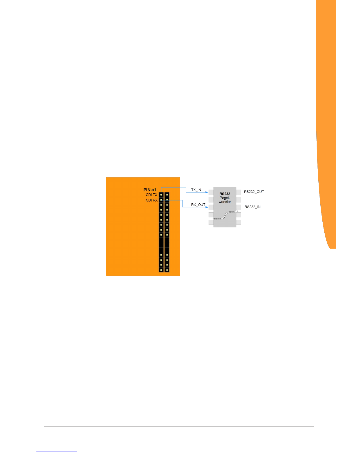
KUNBUS-COM EtherCAT 93 / 135
8 CDI
8.1 Setting up a Serial Connection
The CDI interface of the COMS-Module is a UART interface
(asynchronous serial interface) with 3.3V CMOS signal level.
If you connect a switch with level converter (e.g. "EXAR SP3232EUEY") to the application connector via the RX and TX
connections of this interface, an RS232 interface is available to you
for connecting a terminal (you can find details from our sample circuit
diagram under "RS232 Interface for CDI" in the Appendix).
Illustration12: Setting up a Serial Connection
You can connect the serial COMx interface of a PC to such a
terminal interface (or a serial USB converter) and then access the
CDI menus using a terminal emulation. We provide you with PuTTY
as a terminal emulation on our support webpage.
CDI
Page 94
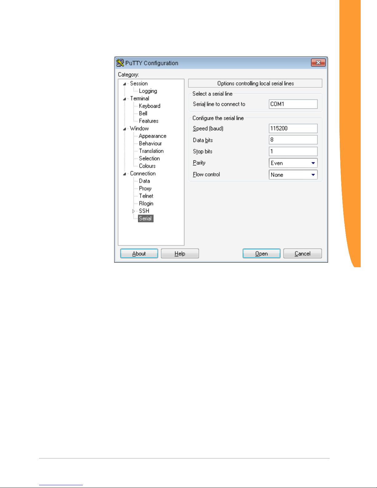
KUNBUS-COM EtherCAT
94 / 135
How to start PuTTY:
Illustration13: Putty Serial
◦ Change to the "Connection > Serial" view
◦ Select the serial interface that you want to access the CDI with (here:
COM1)
◦ Configure the interface with the default settings of the CDI interface (for
values see Fig above). Deactivate the dataflow control as well.
◦ Change to the "Session" view.
◦ Activate "Serial" as connection type. The "Serial line" and "Speed" fields
are already preallocated with the settings you specified beforehand.
◦ Assign a name under "Saved Sessions" to save these settings.
◦ Click on "Save".
◦ Click on "Open".
ð The main menu will open in the terminal window.
NOTICE!If the terminal window remains black, click on the [ESC]
key to start the data transmission via the CDI.
CDI
Page 95
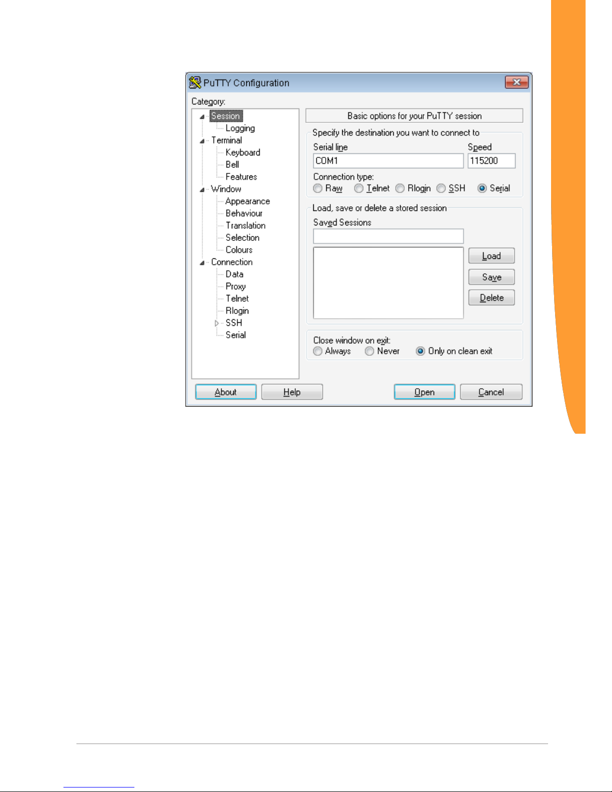
KUNBUS-COM EtherCAT 95 / 135
Illustration14: Putty Session
CDI
Page 96

KUNBUS-COM EtherCAT
96 / 135
8.2 CDI Menus
Main Menu
The main menu is your access point for operating the module using
the CDI. After a reset, the module transmits this main menu to the
terminal.
-------------------------------------------------KUNBUS-COM – Main Menu
-------------------------------------------------1 – Module Information
2 – Interface Configuration
3 - Monitor Communication
4 – Module Status
------------------------------------------------->
Menu 1 – "Module Information"
1.Module Information
In this menu you will find general information about the module:
– Software revision
– Checksum of the firmware
– Serial number of the module
– Module type (unique throughout KUNBUS)
-------------------------------------------------KUNBUS-COM - Module Information
-------------------------------------------------Revision: 2.0.7935
Firmware CRC: 0xdebd4edc
Serial Number: 4294967295
Module Type: ( 29) EtherCAT
------------------------------------------------->
CDI
Page 97

KUNBUS-COM EtherCAT 97 / 135
Menu 2 – "Interface Configuration"
2. Interface Configuration
In this menu you have the option to define the operational
parameters for the different interfaces.
Here, you can set the mapping for the data broker.
Changes that you make in these menus are first activated after a
restart.
The selection "12 – Set Arbitrary Register" allows you
write access to all writeable Modbus registers of the module.
-------------------------------------------------KUNBUS-COM – Interface Configuration
-------------------------------------------------Operating Mode: Running
1 - SDI Communication
2 - CDI Communication
3 - SSC Communication
4 - DPR Configuration
6 - SDI Output mapping
7 - SSC Output mapping
8 - Fieldbus Output mapping
9 - DPR Output mapping
11 - Fieldbus Specific
12 - Set Arbitrary Register
13 - Script Interpreter
14 - Reset Module
15 - Reset to Factory Settings
16 - Extended Mapping
------------------------------------------------->
2.1 SDI Communication
In this menu you will find information about the settings for the
Modbus RTU communication. You can configure the values in the
submenus.
-------------------------------------------------KUNBUS-COM - SDI Communication
-------------------------------------------------1 – Bitrate: Automatic Bitrate detection
2 – Parity: Even Parity, 1 Stopbit
------------------------------------------------->
NOTICE!When the COMS module is in DPR mode, you cannot
configure the SDI settings. The CDI aborts the action with a
corresponding error message.
CDI
Page 98

KUNBUS-COM EtherCAT
98 / 135
2.1.1 SDI Communication
Bitrate
In this menu you have the option, to select the appropriate Bitrate for
your application.
The default value is "Automatic Bitrate detection".
-------------------------------------------------KUNBUS-COM – SDI Communication: Set Bitrate
-------------------------------------------------1 – Automatic Bitrate detection
2 – 2400 Bit/s
3 – 4800 Bit/s
4 – 9600 Bit/s
5 – 19200 Bit/s
6 – 38400 Bit/s
7 – 57600 Bit/s
8 – 115200 Bit/s
------------------------------------------------->
2.1.2 SDI CommunicationSet Parity
In this menu you have the option to select the appropriate parity for
your application from the displayed values.
The default value is "Even Parity (1 stop-bit)".
The number of stop-bits is based automatically on the parity setting.
This ensures that a transmission always contains the same number
of bits per byte.
-------------------------------------------------KUNBUS-COM – SDI Communication: Set Parity
-------------------------------------------------1 – Even Parity (1 Stopbit)
2 – Odd Parity (1 Stopbit)
3 – No Parity (2 Stopbits)
------------------------------------------------->
2.1.3 Set Modbus Node
Address
In this menu you have the option, to enter the Modbus Node
Address.
Permitted input values: 1-247
-------------------------------------------------------KUNBUS-COM - SDI Communication: Set Modbus Node Address
-------------------------------------------------------Enter a Modbus Node Address between 1 and 247:
------------------------------------------------------->
2.2 CDI Communication
In this menu you will find information about the currently set values of
bitrate and parity. In the submenus you can configure the values.
-------------------------------------------------KUNBUS-COM – CDI Communication
-------------------------------------------------1 – Bitrate: 115200 Bit/s
2 – Parity: Even Parity, 1 Stopbit
------------------------------------------------->
CDI
Page 99

KUNBUS-COM EtherCAT 99 / 135
2.2.1 CDI Communication Set Bitrate
In this menu you have the option, to select the appropriate Bitrate for
your application.
The default value is 115200 bit/s.
Automatic bitrate detection via the CDI is not possible.
-------------------------------------------------KUNBUS-COM – CDI Communication: Set Bitrate
-------------------------------------------------1 – 2400 Bit/s
2 – 4800 Bit/s
3 – 9600 Bit/s
4 – 19200 Bit/s
5 – 38400 Bit/s
6 – 57600 Bit/s
7 – 115200 Bit/s
------------------------------------------------->
2.2.2 CDI Communication Set Parity
In this menu you have the option to select the appropriate parity for
your application from the displayed values.
The default value is "Even Parity (1 stop-bit)".
The number of stop-bits is based automatically on the parity setting.
This ensures that a transmission always contains the same number
of bits per byte.
-------------------------------------------------KUNBUS-IC - CDI Communication: Set Bitrate
-------------------------------------------------1 - Even Parity, 1 Stopbit
2 - Even Parity, 2 Stopbit
3 - Odd Parity, 1 Stopbit
4 - Odd Parity, 2 Stopbit
5 - No Parity, 1 Stopbit
6 - No Parity, 2 Stopbit
------------------------------------------------->
CDI
Page 100

KUNBUS-COM EtherCAT
100 / 135
SSC Mode
In this menu you have the option, to configure the shift register chain.
You can choose between the following modes using the Direction Pin
(b2):
– SSC SSR Master Mode (Default value, Direction Pin not set)
– SSC SPI Slave Mode (Direction Pin set)
2.3 Select SSC SSR Master
Mode
Prerequisite: The Direction Pin (b2) is not set. As a result, the
master mode is active.
In this menu you have the following options:
– SSC SSR Master Mode, disabled: With this option, you switch off the
SSC.
– SSC SSR Master Mode, auto detect shift registers: With this option, the
number of input/output shift registers and the bitrate is determined
automatically.
– SSC SSR Master Mode, configured shift registers: With this option, you
can define the number of input/output shift registers and the bitrate
yourself.
– Enter [3] + [Enter] to select this mode as the configuration source.
– With the option [9] you open the configuration menu.
-------------------------------------------------KUNBUS-COM- Select SSC SSR Master Mode
-------------------------------------------------Mode: SSC SSR Master Mode, configured shift registers
1 - SSC SSR Master Mode, disabled
2 - SSC SSR Master Mode, auto detect shift registers
3 - SSC SSR Master Mode, configured shift registers
------------------------------------------------->
2.3.3 SSC SSR Master Mode,
configure shift registers
Prerequisite: In menu "2.3 - Select SSC SSR Master Mode" you
have selected the configuration source "SSC SSR Master Mode,
configure shift registers".
In this menu you have the following options:
– Number of input shift registers
– Number of output shift registers
– Bitrate
-------------------------------------------------KUNBUS-COM- SSC SSR Master Mode, configure shift registers
-------------------------------------------------1 - Number of overall Input Registers: 0
2 - Number of overall Output Registers: 0
3 - Configured Bitrate: 300 kBit/s
------------------------------------------------->
CDI
 Loading...