

Page 1
2.4 GHz antenna all-in-one design RF module
WR RF module
Manual
Specifications and appearance are subject to change without notice for improvement
KORG INC.
4015-2 Yanokuchi, Inagi-city, Tokyo 206-0812, Japan
Page 2
1 Introduction
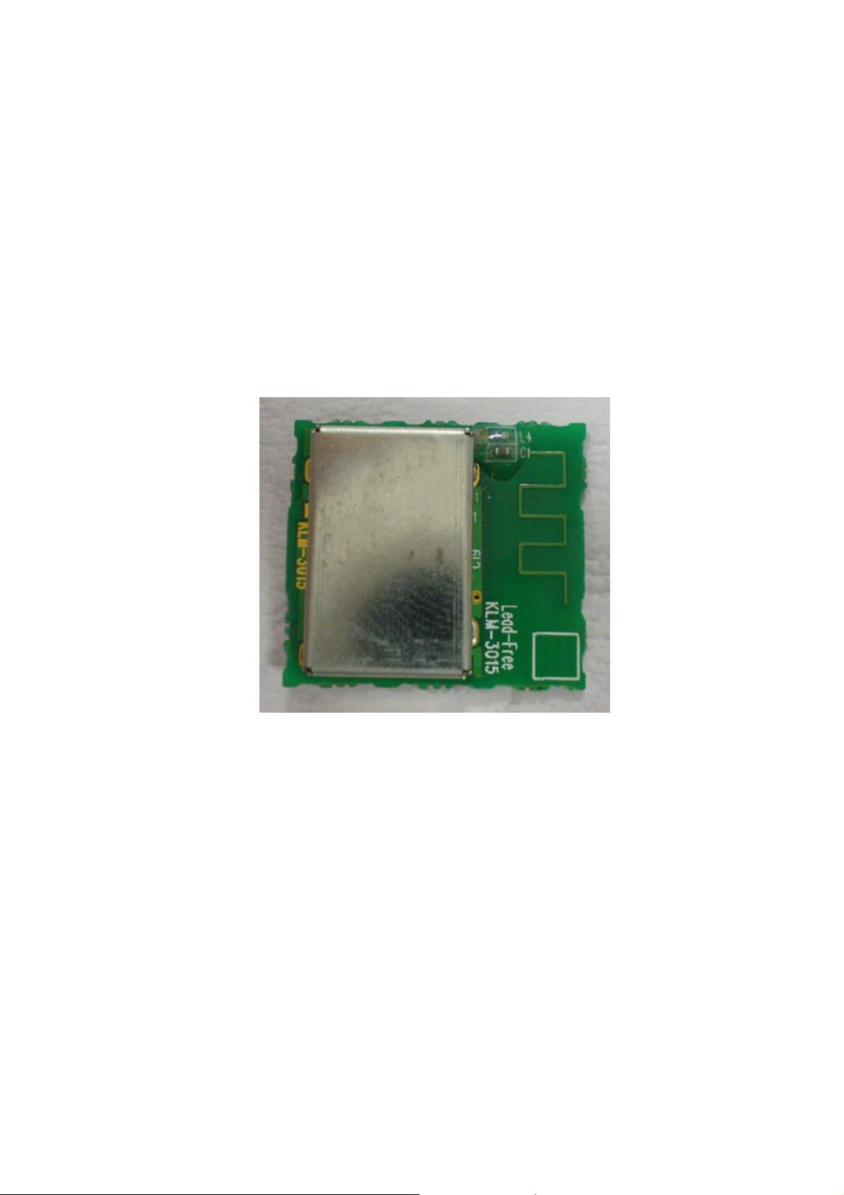
The WR RF module is a 2.4GHz transceiver.
WR RF module operates in 2.400-2.4835GHz ISM frequency band.
To design a radio system with the WR RF module, you simply need an MCU (microcontroller)
and a few external passive components.
You can operate and configure the WR RF module through a Serial Peripheral Interface (SPI).
1.1 Features
Features of the nRF24L01+ include:
• Radio
Worldwide 2.4GHz ISM band operation
Common RX and TX interface
GFSK modulation
2Mbps air data rate
• Power Management
Integrated voltage regulator
1.9 to 3.6V supply range
1.2 Product specification
This module carries RF device nRF24L01P made in NORDIC company.
Please refer to a nRF24L01P data sheet submitted by NORDIC company ab out the details of the
RF device.
The main specifications of this RF module are shown as follows.
Function Item Main specifications
Use device nRF24L01P made in NORDIC company
Frequency band 2405MHz~2480MHz
Antenna electricity Max. 0dBm
General specifications
Oscillation
Power supply voltage +1.9V~+3.6V(Normal +3.0V)
External form dimensions 20.5±0.3 x 18.5±0.3 X 4.2±0.3 [mm]
Weight 1.3g
Operating temperature 0℃~40℃
Transmitting power Max. 0dBm
RF transmission part
Frequency deviation 50ppm or less
Modulation method GFSK
RF reception part Frequency deviation 50ppm or less
Built-in Pattern antenna
Antenna
Form Monopole λ/4
Directivity No directivity
User outside interface Serial communication SPI-IF
Crystal oscillation 16MHz are built in it
(A PLL frequency synthesizer method)
Page 3
a
2 Module specifications
2.1 Partial explanation
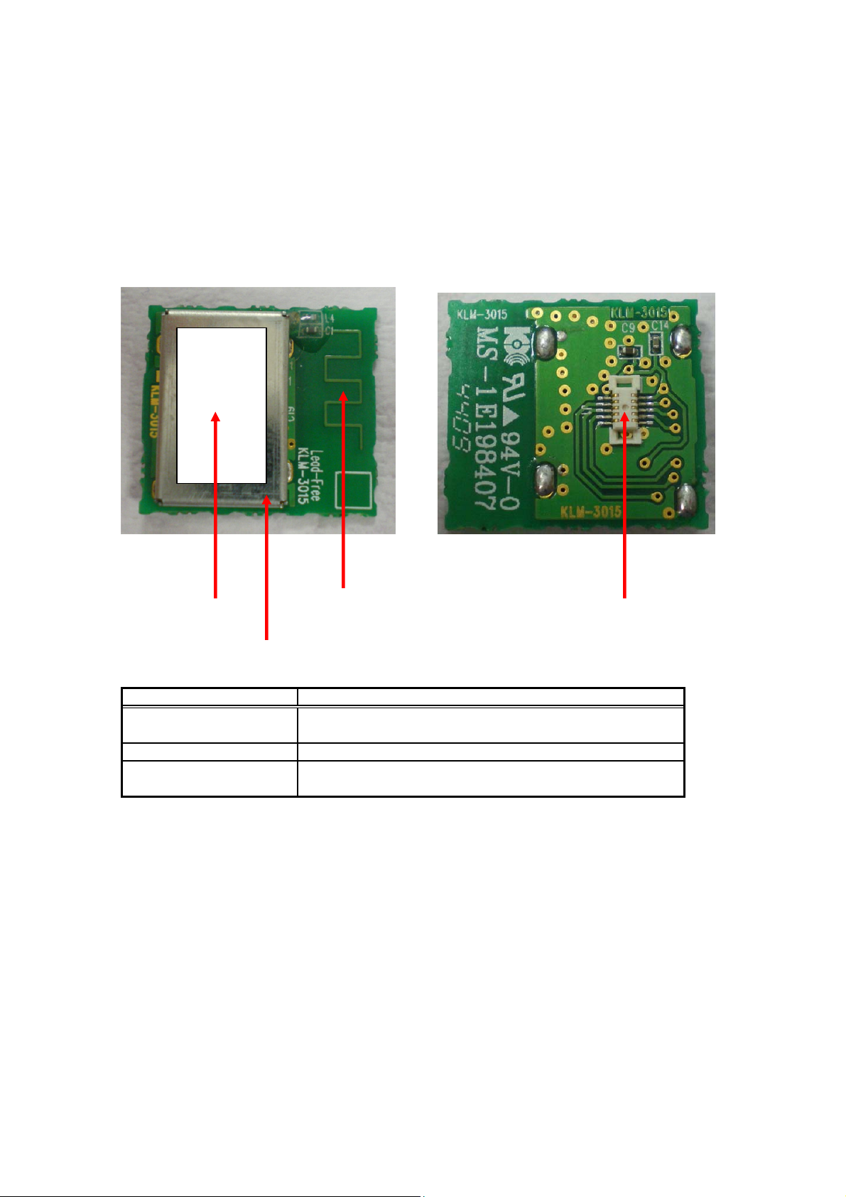
Each part of this module is explained.
Proof seal 2.4 GHz monopole antenna User interface connector
Shield cover
Part Explanation
2.4 GHz monopole antenn
Proof seal
User interf ace c onnect or
Attention:
Please do not put the label etc. on the antenna.
When the seal and the label are put on the antenna, the characteristic of the antenna
might be ruined.
It is a built-in antenna of the RF module.
The antenna is made by the copper foil pattern of PCB.
It is the certification label of this module.
It is an interface connector to use in a user.
Please refer to interface specifications for the details.
Page 4

2.2 Interface specification
The offered interface is shown below.
Mounting connector: Narrow Pitch Connector (0.5 mm pitch) Header AXK6F10347YG Panasonic
Combination connector: Narrow Pitch Connector (0.5 mm pitch) Socket AXK5F10xx7YG Panasonic
Pin functions
①
②
③
④
⑤
⑩
⑨
⑧
⑦
⑥
Pin Name Pin function Description
1 VDD Power Power Supply (+1.9V - +3.6V DC)
2 IRQ Digital Output Maskable interrupt pin. Active low
3 MISO Digital Output SPI Slave Data Output, with tri-state option
4 MOSI Digital Input SPI Slave Data Input
5VSS Power Ground (0V)
6VSS Power Ground (0V)
7 SCK Digital Input SPI Clock
8 CSN Digital Input SPI Chip Select
9 CE Digital Input Chip Enable Activates RX or TX mode
10 VDD Power Power Supply (+1.9V - +3.6V DC)
Strict observance: The power supply connection must not make a mistake.
The protection circuit in the power supply part is not installed in this module.
There is fear of damage, and note the polarity and the voltage of the power
supply enough, please.
Please do not touch the terminal of this module directly by the hand.
The inside might be destroyed by static electricity.
Page 5

3 Electrical specifications
Conditions: VDD = +3V, VSS = 0V, TA = - 40ºC to + 85ºC
3.1 Absolute maximum ratings
Note: Exceeding one or more of the limiting values may cause permanent damage to WR RF
module.
Operating conditions Minimum Maximum Units
Supply voltages
VDD -0.3 3.6 V
VSS 0 V
Input voltage
VI -0.3 5.25 V
Output voltage
VO VSS to VDD VSS to VDD
Total Power Dissipation
PD (TA=85°C) 60 mW
Temperatures
Operating Temperature 0 40 ℃
3.2 DC characteristics
Symbol Parameter (condition) Notes Min. Typ. Max. Units
Operating conditions
VDD Supply voltage 1.9 3.0 3.6 V
VDD Supply voltage if input signals >3.6V 2.7 3.0 3.3 V
Digital input pin
VIH HIGH level input voltage a 0.7VDD 5.25 V
VIL LOW level input voltage VSS 0.3VDD V
Digital output pin
VOH HIGH level output voltage (IOH=-0.25mA) VDD -0.3 VDD V
VOL LOW level output voltage (IOL=0.25mA) 0.3 V
Power on reset
TPUP Power ramp up time b 100 ms
TPOR Power on reset c 1 100 ms
a. If the input signal >3.6V, the VDD of the nRF24L01+ must be between 2.7V and 3.3V (3.0V±10%)
b. From 0V to 1.9V.
c. Measured from when the VDD reaches 1.9V to when the reset finishes.
Page 6

3.3 Power consumption
Symbol Parameter (condition) Min. Typ. Max. Units
Idle modes
IVDD_PD Supply current in power down mode 900 nA
IVDD_SU Average current during 1.5ms crystal oscillator startup 400uA
Transmit
IVDD_TX0 Supply current @ 0dBm output power 11.3 mA
IVDD_TX6 Supply current @ -6dBm output power 9.0 mA
IVDD_TX12 Supply current @ -12dBm output power 7.5 mA
IVDD_TX18 Supply current @ -18dBm output power 7.0 mA
Receive
IVDD_2M Supply current 2Mbps 13.5 mA
4 Appendix
4.1 Dimensional outline drawing
18.5mm
±0.3mm
20.5mm±0.3mm
Attention: Please do not make the pattern under the antenna of this module.
(Might it influence the antenna part if the pattern is made, and the communication
distance performance be ruined.)
Page 7

4.2 For technical standard certification of conformity
Please paste the proof seal to include "IC: 8689A-WRRF” "FCC ID: KIJ-WRRF "" on the module
shield cover.
Label for end product must include “Contains FCC ID: KIJ-WRRF” “Contains IC: 8689A-WRRF”.
CHANGED OR MODIFICATIONS NOT EXPRESSLY APPROVED BY THE MANUFACTURER
FOR COMPLIANCE COULD VOID THE USER'S AUTHORITY TO OPERATE THE
EQUIPMENT
This equipment has been tested and found to comply with the limits for a Class B digital device,
pursuant to part 15 of the FCC rules. These limits are designed to provide reasonable protection
against harmful interference in a residential installation. This equipment generates, u ses and can
radiate radio frequency energy and, if not installed and used in accordance with the instructions,
may cause harmful interference to radio communications. However, there is no guarantee that
interference will not occur in a particular installation. If this equipment does cause harmful
interference to radio or television reception, which can be determined by turning the equipment
off and on, the user is encouraged to try to correct the interference by one or more of the
following measures:
-Reorient or relocate the receiving antenna.
-Increase the separation between the equipment and receiver.
-Connect the equipment into an outlet on a circuit different from that to which the receiver is
connected.
-Consult the dealer or an experienced radio/TV technician for help.
This device complies with Part 15 of the FCC Rules. Operation is subject to the following two
conditions: (1) this device may not cause harmful interference and (2) this device must accept
any interference received, including interference that may cause undesired operation
Page 8

Complies with Canadian ICES-003 Class B.
Conforme au Reglement Canadian NMB-003 classe B.
Operation is subject to the following two conditions: (1) this device may not cause interference,
and (2) this device must accept any interference, including interference that may cause
undesired operation of this device.
L ‘ utilisation de ce dispositif est autorisée seulement aux conditions suivantes:
(1) il ne doit pas produire de brouillage et
(2) l’ utilisateur du dispositif doit étre prêt à accepter tout brouillage radioélectrique reçu, meme si
ce brouillage est susceptible de compromettre le fonctionnement du dispositif.
The installer of this radio equipment must ensure that the antenna is located or pointed such that
it does not emit RF field in excess of Health Canada limits for the general population; consult
Safety Code 6, obtainable from Health Canada’s website www.hc-sc.gc.ca/rpb
 Loading...