

Page 1

PB-DOUT8
Eight-Channel Digital I/O
ModPack Piggyback
Manual ID 17984, Index 0110
Oct 98
Page 2

This page was intentionally left blank.
ID 17984, Index 0110
Page 3

PB-DOUT8
Preface
Preface
Revision History............................................................. 0-6
For Your Safety.............................................................. 0-5
Special Handling and Unpacking Instructions............ 0-5
HV Safety Instructions................................................ 0-6
Two Years Warranty ...................................................... 0-7
Table of Contents........................................................... 0-8
Oct 98
Page 0 - 3ID 17984, Index 0110
Page 4
Preface
Revision History
Manual/Product Title: PB-DOUT8
Manual ID Number: 17984
PB-DOUT8
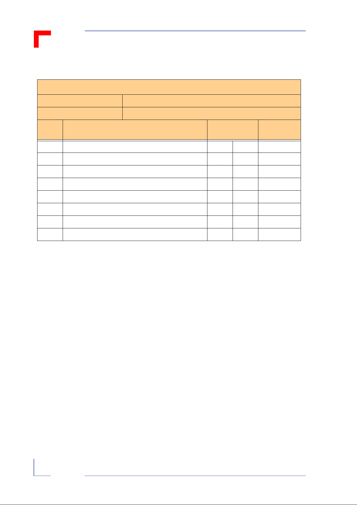
REVISION HISTORY
Rev.
Index
0100 Initial Issue 01 01 Mar 98
0110 Chapters 1, 1.1, 1.5, 4.2, 4.3 et al. 01 01 Oct. 98
This document contains proprietary information of PEP Modular Computers. It may not be
copied or transmitted by any means, passed to others, or stored in any retrieval system or
media, without the prior consent of PEP Modular Computers or its authorized agents.
The information in this document is, to the best of our knowledge, entirely correct. However,
PEP Modular Computers cannot accept liability for any inaccuracies, or the consequences
thereof, nor for any liability arising from the use or application of any circuit, product, or example shown in this document.
Brief Description of Changes PCB Index Date of
Issue
PEP Modular Computers reserve the right to change, modify, or improve this document or the
product described herein, as seen fit by PEP Modular Computers without further notice.
Page 0 - 4
Oct 98ID 17984, Index 0110
Page 5

PB-DOUT8
Preface
For your safety
This PEP product is carefully designed for a long, fault-free life. However, its life expectancy
can be drastically reduced by improper treatment during unpacking and installation. Therefore, in the interest of your own safety and of correct operation of your new PEP product,
please take care of the following guidelines:
$ Before installing your new PEP product into a system, please, always switch off your
power mains. This applies also to installing piggybacks.
$ In order to maintain PEP’s product warranty, please, do not alter or modify this product
in any way. Changes or modifications to the device, which are not explicitly approved by
PEP Modular Computers and described in this manual or received from PEP Technical
Support as a special handling instruction, will void your warranty.
$ This device should only be installed in or connected to systems that fulfil all necessary
technical and specific environmental requirements. This applies also to the operational
temperature range of the specific board version, which must not be exceeded. If batteries are present, their temperature restrictions must be taken into account.
$ In performing all necessary installation and application operations, please, follow only
the instructions supplied by the present manual.
$ Keep all the original packaging material for future storage or warranty shipments. If it is
necessary to store or ship the board, please, re-pack it in the original way.
Special Handling and Unpacking Instructions
Electronic boards are sensitive to static electricity. Therefore, care must be taken during all
handling operations and inspections with this product, in order to ensure product integrity at all
times.
$ Do not handle this product out of its protective enclosure while it is not being worked
with, or unless it is otherwise protected.
$ Whenever possible, unpack or pack this product only at EOS/ESD safe work stations.
$ Where safe work stations are not guaranteed, it is important for the user to be electri-
cally discharged before touching the product with his/her hands or tools. This is most
easily done by touching a metal part of your system housing.
$ Particularly, observe standard anti-static precautions when changing piggybacks, ROM
devices, jumper settings etc. If the product contains batteries for RTC or memory backup, ensure that the board is not placed on conductive surfaces, including anti-static
plastics or sponges. They can cause short circuits and damage the batteries or tracks
on the board.
Oct 98
Page 0 - 5ID 17984, Index 0110
Page 6

Preface
PB-DOUT8
Safety Instructions for High Voltages
This chapter of the safety instructions applies to HV appliances (> 60 V) only.
Your new PEP product was developed and tested carefully to provide all features necessary
to ensure the renown electrical safety requirements. However, serious electrical shock hazards exist during all installation, repair and maintenance operations with this product. Therefore, always unplug the power cable to avoid exposure to hazardous voltage.
All operations on this device have to be carried out by sufficiently skilled personnel only.
Page 0 - 6
Oct 98ID 17984, Index 0110
Page 7

PB-DOUT8
Preface
Two Years Warranty
PEP Modular Computers grants the original purchaser of PEP products a TWO YEARS LIMITED
HARDWARE WARRANTY as described in the following. However, no other warranties that may
be granted or implied by anyone on behalf of PEP are valid unless the consumer has the
expressed written consent of PEP Modular Computers.
PEP Modular Computers warrants their own products, excluding software, to be exempt of
manufacturing and material defects for a period of 24 consecutive months from the date of
purchase. This warranty is not transferable nor extendible to cover any other users or longterm storage of the product. It does not cover products which have been modified, altered or
repaired by any other party than PEP Modular Computers or their authorized agents. Furthermore, any product which has been, or is suspected of being damaged as a result of negligence, improper use, incorrect handling, servicing or maintenance, or which has been
damaged as a result of excessive current/voltage or temperature, or which has had its serial
number(s), any other markings or parts thereof altered, defaced or removed will also be
excluded from this warranty.
If the customer’s eligibility for warranty has not been voided, in case of any claim, he may
return the product at the earliest possible convenience to the original place of purchase,
together with a copy of the original document of purchase, a full description of the application
the product is used on and a description of the defect. Pack the product in such a way as to
ensure safe transportation (see our safety instructions).
PEP provides for repair or replacement of any part, assembly or sub-assembly at their own
discretion, or to refund the original cost of purchase, if appropriate. In the event of repair,
refunding or replacement of any part, the ownership of the removed or replaced parts reverts
to PEP Modular Computers, and the remaining part of the original guarantee, or any new
guarantee to cover the repaired or replaced items, will be transferred to cover the new or
repaired items. Any extensions to the original guarantee are considered gestures of goodwill,
and will be defined in the “Repair Report” issued by PEP with the repaired or replaced item.
PEP Modular Computers will not accept liability for any further claims resulting directly or indirectly from any warranty claim, other than the above specified repair, replacement or refunding. Particularly, all claims for damage to any system or process in which the product was
employed, or any loss incurred as a result of the product not functioning at any given time, are
excluded. The extent of PEP Modular Computers liability to the customer shall not exceed the
original purchase price of the item for which the claim exist.
PEP Modular Computers issues no warranty or representation, either explicit or implicit, with
respect to its products, reliability, fitness, quality, marketability or ability to fulfil any particular
application or purpose. As a result, the products are sold “as is,” and the responsibility to
ensure their suitability for any given task remains of the purchaser. In no event will PEP be liable for direct, indirect or consequential damages resulting from the use of our hardware or
software products, or documentation, even if PEP were advised of the possibility of such
claims prior to the purchase of the product or during any period since the date of its purchase.
Please remember that no PEP Modular Computers employee, dealer or agent is authorized to
make any modification or addition to the above specified terms, either verbally or in any other
form written or electronically transmitted, without the company’s consent.
Oct 98 Page 0 - 7ID 17984, Index 0110
Page 8

Preface
Table of Contents
PB-DOUT8
Chapt
Chapter
1. Introduction.............................................................1 - 3
1.1 EMC Compliance..............................................1 - 3
1.2 Board Overview................................................1 - 3
1.3 Main Features...................................................1 - 4
1.4 Board Layout ....................................................1 - 5
1.5 Technical Specification.....................................1 - 6
Chapter
2. Configuration..........................................................2 - 3
2.1 Pinout................................................................2 - 3
1
1
2
2.2 Jumper Configuration .......................................2 - 5
Chapter
3. Installation ..............................................................3 - 3
3.1 Carrier Board Interfacing ..................................3 - 3
3.2 Carrier Board Installation..................................3 - 6
3
Page 0 - 8
Oct 98ID 17984, Index 0110
Page 9

PB-DOUT8
Preface
Chapter
4. Software References..............................................4 - 3
4.1 Technical Features...........................................4 - 3
4.2 Memory Map.....................................................4 - 3
4.3 PB-DOUT8 Registers.......................................4 - 4
4.4 Error Analysis...................................................4 - 6
4
Oct 98
Page 0 - 9ID 17984, Index 0110
Page 10

This page was intentionally left blank.
ID 17984, Index 0110
Page 11

PB-DOUT8
Introduction
Introduction
1.1EMC Compliance ................................................................. 1 - 3
1.2Board Overview....................................................................1 - 3
1.3Main Features ...................................................................... 1 - 4
1.3.1High-Side Power Switches............................................1 - 4
1.3.2Low-Side Power Switches............................................. 1 - 5
1.3.3Board Interfaces............................................................1 - 5
1.4Board Layout........................................................................ 1 - 5
Chapter
1
1.5Technical Specification......................................................... 1 - 6
22 Oct 98
Page 1 - 1Man. ID 17984, Rev. Index 0110
Page 12

This page was intentionally left blank.
Man. ID 17984, Rev. Index 0110
Page 13

PB-DOUT8
Introduction
1. Introduction
The PB-DOUT8 is a single-size ModPack piggyback (100 mm x 48 mm) designed to fit
any of the following carrier boards of the PEP Modular Computers ModPack range:
• VMOD
• VMOD-2/VMOD-2D,VMOD-4D
• VM642/662
• CXM-IMOD
It will also, where possible and appropriate, be compatible with future Modpack boards
The PB-DOUT8 is an 8-channel digital output module utilising “intelligent” power transis-
tors which prevent damage to the circuitry resulting from exposure to the following factors:
• overload;
• undervoltage and overvoltage;
• short circuit;
• overtemperature;
• electrostatic discharges.
In addition, the PB-DOUT8 module is provided with open-load detection.
1.1 EMC Compliance
The PB-DOUT8 piggyback module complies with the requirements of the following CErelevant standards:
• Emission: EN50081-1;
• Immission: EN50082-2;
• Electrical Safety: EN60950.
1.2 Board Overview
PB-DOUT8 is a piggyback output module consisting of eight channels with high-side
and eight channels with low-side switches. Each channel has its own status bit. The
switches are divided into four separate groups, each group having individual power supply (up to 40 V) and grounding. The channel groups are galvanically isolated from one
another and towards the VMEbus.
The output channels switch direct current, namely 1.3 A on the low side and 1.8 A on
the high side, although the minimum output current may vary with different temperatures
(see table 2-1 for exact figures). The maximum (peak) output current is instead typically
4.0 A on the low side and 5.0 A on the high side. The output voltage is typically 24 V DC.
22 Oct 98
Page 1 - 3Man. ID 17984, Rev. Index 0110
Page 14

PB-DOUT8
!
Introduction
The board interrupts, which are hard-coded, are generated and handled according to
various smart transistor conditions.
Attention!
Please check the specification of your carrier board to make sure
that it supports the output current of the PB-DOUT8.
PB-DOUT8 does not have a reverse voltage protection for the external 24 V power supply lines.
Figure 1-1: PB-DOUT8 Functional Block Diagram
CARRIER BOARDCARRIER BOARD
High-side
STAT
OUT
Power
Switches
LOGIC
IN
GND
External IF
Legend:
STAT = status
GND = ground
Process IF
PBDOUT-8PBDOUT-8
Low-side
Power
Switches
Opto-Coupling
ModPack IF
VME Bus IF
1.3 Main Features
In the following the main features of the principal functional blocks of the PB-DOUT8
digital output module are described.
1.3.1 High-Side Power Switches
The PB-DOUT8 module is provided with eight Siemens BTS412B2 smart power transistors for high-side switching having the following features:
• overload protection
• current limitation
• short-circuit protection
• thermal shutdown
• undervoltage and overvoltage shutdown
• open-load detection
• loss-of-ground protection
• ESD protection
Page 1 - 4
22 Oct 98Man. ID 17984, Rev. Index 0110
Page 15

PB-DOUT8
!
Introduction
1.3.2 Low-Side Power Switches
The PB-DOUT8 module is provided with four two-channel Siemens TLE 5224 G2 smart
power transistors for low-side switching having the following features:
• overload protection
• power limitation
• short-circuit protection
• overtemperature monitoring
• overvoltage protection
• ESD protection
1.3.3 Board Interfaces
The PB-DOUT8 piggyback module is provided with two digital I/O connectors. The one
on the input side is a 15-pin double-row connector, the one on the process side a 12-pin
double-row connector. The input connector is wired via the carrier board to a 50-pin
DSUB or to a 50-pin FB connector, while the process interface is wired to the carrier
board’s VMEbus socket.
Attention!
In fitting your PB-DOUT8 piggyback module onto its carrier board,
please make sure the PB-DOUT8 pin rows match the corresponding rows of pinholes of the carrier board socket (see chapter 3).
1.4 Board Layout
Figure 1-2: PB-DOUT8 Board Layout — Component Side (Left) and Solder Side (Right)
30
High-side
ST2
1
LOGIC
OPTO-COUPLERS
Power
Switches
24
ST1
1
22 Oct 98
Legend:
NSR = Not system-relevant
Low-side
Power
Switches
(NSR)
Page 1 - 5Man. ID 17984, Rev. Index 0110
Page 16

PB-DOUT8
1.5 Technical Specification
Table 1-1: PB-DOUT8 Technical Specification
PB-DOUT8 Specification
Introduction
Channels and Channel
Grouping
Isolation Voltages Group-to-group: 0.7 mm (0.7 kV)
Input Voltage Range: 10...40 V DC
Power Consumption 24V side:typ. 2mA per group
Temperature Range:
- Standard Operation
- Extended Operation
- Storage
Driving Current Typically: 1.3 A DC (low side),
Open Circuit Detection Typ. 30 µA
4 groups of channels, each consisting of
- 2 channels with high-side switches
- 2 channels with low-side switches
Group-to-VMEbus:4.0 mm (4.0 kV)
Nominal: 24 V DC
VMEbus side:typ. 95 mA
0° to + 70°C
- 40° to + 85°C
- 55° to + 125°C
1.8 A DC (high side)
Minimum (LS/HS): 1.0 A DC (0...+70°C)
0.6 A DC (-40...0°C)
Maximum (typ.) 4.0 A (low side),
5.0 A (high side)
Operating Frequency 0...250 Hz, incl. inductive load
Inductive Load 24 V/0.5 A/1,0 Henry
On-State Resistance Typically: 250 mOhm (low side),
220 mOhm (high side)
Switching Speed Typ. 1 ms, incl. status feedback
Page 1 - 6
22 Oct 98Man. ID 17984, Rev. Index 0110
Page 17

PB-DOUT8
Configuration
Configuration
2.1Pinout................................................................................... 2 - 3
2.2Jumper Configuration........................................................... 2 - 5
Chapter
2
22 Oct 98
Page 2 - 1Man. ID 17984, Rev. Index 0110
Page 18

This page was intentionally left blank.
Man. ID 17984, Rev. Index 0110
Page 19

PB-DOUT8
Configuration
2. Configuration
2.1 Pinout
The PBDOUT-8 is connected via its carrier board to a 50-way flat-band cable or DSUB
connector. Depending on the carrier board location where the piggyback is installed (“A”
of “B”), either the upper half or the lower half of the connector pins are used
The following tables show the output registers and the corresponding output lines for the
upper (“A”) and lower (“B”) location, with reference to the relative DSUB/FB connectors
of the carrier board:
Table 2-1: PB-DOUT8 Pinout (Lower Position)
Pin DSUB 50 FB 50 Pin DSUB 50 FB 50
OUT07L Pin 1 Pin 1 OUT03L Pin 5 Pin 13
OUT07H Pin 34 Pin 2 OUT03H Pin 38 Pin 14
OUT06L Pin 18 Pin 2 OUT02L Pin 22 Pin 15
OUT06H Pin 2 Pin 4 OUT02H Pin 6 Pin 16
GND0607 Pin 35 Pin 5 GND0203 Pin 39 Pin 17
VSS0607 Pin 19 Pin 6 VSS0203 Pin 23 Pin 18
OUT05L Pin 3 Pin 7 OUT01L Pin 7 Pin 19
OUT05H Pin 36 Pin 8 OUT01H Pin 40 Pin 20
OUT04L Pin 20 Pin 9 OUT00L Pin 24 Pin 21
OUT04H Pin 4 Pin 10 OUT00H Pin 8 Pin 22
GND0405 Pin 37 Pin 11 GND0001 Pin 41 Pin 23
VSS0405 Pin 21 Pin 12 VSS0001 Pin 25 Pin 24
22 Oct 98
Page 2 - 3Man. ID 17984, Rev. Index 0110
Page 20

PB-DOUT8
Table 2-2: PB-DOUT8 Pinout (Upper Position)
Pin DSUB 50 FB 50 Pin DSUB 50 FB 50
OUT07L Pin 26 Pin 27 OUT03L Pin 30 Pin 39
OUT07H Pin 10 Pin 28 OUT03H Pin 14 Pin 40
OUT06L Pin 43 Pin 29 OUT02L Pin 47 Pin 41
OUT06H Pin 27 Pin 30 OUT02H Pin 31 Pin 42
GND0607 Pin 11 Pin 31 GND0203 Pin 15 Pin 43
VSS0607 Pin 44 Pin 32 VSS0203 Pin 48 Pin 44
OUT05L Pin 28 Pin 33 OUT01L Pin 32 Pin 45
OUT05H Pin 12 Pin 34 OUT01H Pin 16 Pin 46
OUT04L Pin 45 Pin 35 OUT00L Pin 49 Pin 47
Configuration
OUT04H Pin 29 Pin 36 OUT00H Pin 33 Pin 48
GND0405 Pin 13 Pin 37 GND0001 Pin 17 Pin 49
VSS0405 Pin 46 Pin 38 VSS0001 Pin 50 Pin 50
Figure 2-1: Pin Numbering of DSUB 50 and Front Panel Connector (FB 50)
Pin 33
Pin 50
Pin 34 Pin 1
Pin 18
Pin 17
Even pins
Pin 50
Pin 2
VMOD
2
Odd pins
Pin 49
Pin 1
Page 2 - 4
DSUB 50
FB 50
22 Oct 98Man. ID 17984, Rev. Index 0110
Page 21

PB-DOUT8
2.2 Jumper Configuration
The PB-DOUT8 module does not have any jumpers to be configured.
Configuration
22 Oct 98
Page 2 - 5Man. ID 17984, Rev. Index 0110
Page 22

This page was intentionally left blank.
Man. ID 17984, Rev. Index 0110
Page 23

PB-DOUT8
Installation
Installation
3.1Carrier Board Interfacing...................................................... 3 - 3
3.1.1Carrier Board VMEbus Connector BU1A/B................... 3 - 4
3.1.2Carrier Board External Interface Connector BU2A/B.... 3 - 4
3.2Carrier Board Installation...................................................... 3 - 6
Chapter
3
22 Oct 98
Page 3 - 1Man. ID 17984, Rev. Index 0110
Page 24

This page was intentionally left blank.
Man. ID 17984, Rev. Index 0110
Page 25

PB-DOUT8
$$
Installation
3. Installation
3.1 Carrier Board Interfacing
This section shows how to proceed with the installation of the PB-DOUT8 piggyback
module on a carrier board. Figure 2-2 shows an example configuration where two piggybacks standing in this case for two PB-DOUT8 modules are fit to a VMOD-2. The first
PB-DOUT8 on a carrier board would fit in the upper position (“A”), the second in the
lower position (“B”).
At first the two header-type connectors (BU1a/BU1b and BU0a/BU0b) of the carrier
board are illustrated, which directly interface to the PB-DOUT8 ST1 pin rows. The lower
case letters in the socket numbers refer to which piggyback location the connector is
used for, e.g. BU1a is socket 1 for PB-DOUT8 location “A”. An illustration showing in
detail all carrier board connectors concerning piggyback installation is given below.
Important!
Please take care to note that the denominations “ST1” and “ST2”
used for the PB-DOUT8 refer only to the piggyback pin row connectors themselves and fit to headers BU1a and BU2a or, respectively,
BU1b and BU2b on the carrier board.
Also the carrier boards have plugs called “ST1” (VMEbusVMEbus
connector) and “ST2” (50-way header), which have no direct relationship to those of the PB-DOUT8 connectors described in this
manual.
Figure 3-1: Carrier Board Connector Denominations
BU2a 26-way, 2-row
piggyback socket for
upper piggyback
ST3 front panel
connector (50-way)
— or —
ST2 on-board
50-way header
BU1a/BU0a 30/45-way
2/3-row upper
piggyback socket
ST1 VMOD-2's
VMEbus 96-way
connector (P1, J1)
22 Oct 98
BU2b 26-way, 2-row
piggyback socket for
lower piggyback
BU1b/BU0b 30/45-way
2/3-row lower
piggyback socket
Page 3 - 3Man. ID 17984, Rev. Index 0110
Page 26

PB-DOUT8
!
3.1.1Carrier Board VME Bus Connector BU1A/B
The Modpack carrier boards are provided with a three-row 45-pin socket. Some piggyback modules, like for instance PB-DOUT8, use only the first two rows (30 pins) of the
header, while other piggybacks, having three-row headers, use also the third row. For
this reason, the first two rows of the connector are named as if they were a separate
socket — “BU1”; the remaining third row instead is called “BU0”.
Attention!
When installing your PB-DOUT8 on its carrier board, please make
sure the piggyback’s pin rows match with the carrier board’s headers as is shown in the following figure.
Figure 3-2: Correct Installation of PB-DOUT8 on the Carrier Board
ST2 ST1
Installation
PB-DOUT8PB-DOUT8
XX
Carrier BoardCarrier Board
BU2 BU1 - 0
3.1.2 Carrier Board External Interface Connector BU2A/B
The 26-pin double-row sockets are totally isolated from the remaining circuits of the carrier board and only connect the output side of the PB-DOUT8 26-pin output header
directly to the upper or lower half of the carrier board’s 50-way front panel connector.
For a better understanding, an overview of piggyback connection in general to VMOD/
VMOD-2 is given in figure 3-3.
Page 3 - 4
22 Oct 98Man. ID 17984, Rev. Index 0110
Page 27

PB-DOUT8
Figure 3-3: PB-DOUT8 Carrierboard Connection
Installation
VMOD-2's ST2 (on-board)
50-way Header
Pin 50
Even
pins
Pin 2
VMOD
2
Pin 49
VMOD-2's ST3
Front Panel
Connector
(50-Way )
Odd
pins
Pin 1
VMOD-2's two 26-way
Headers BU2a (upper)
BU2b (lower)
PB-DOUT8
Position A
(ready for fitting)
Fitted PB-REL
Position B
VMOD-2's two 30/45-way
Header BU1/0a (upper PB)
BU1/0b (lower PB location)
VMOD's ST1
VMEbus
Connector
(96-Way )
PB's ST2
Short
Connector
(26-Way)
26
Even
Pins
2
25
Odd
Pins
1
PB-REL
PB-DOUT8
(ready for fitting)
(ready for fitting)
PB's ST2 and ST1
pin distribution as
seen from the PB's
component side.
!
Remember the PB's
ST2 pin numbers
have nothing to do
with the VMOD-2
ST2's (user I/O) pins.
30
Even
Pins
2
PB's ST1
Long
Connector
(30-Way)
29
Odd
Pins
1
22 Oct 98
Page 3 - 5Man. ID 17984, Rev. Index 0110
Page 28

PB-DOUT8
Installation
3.2 Carrier Board Installation
After the installation of the PB-DOUT8 piggyback on its carrier board, the latter has to
be configured and installed. Please refer to your carrier board’s user manual for configuration and installation of the latter.
Attention!
Please refer to your carrier board’s user manual also for
all security advice on high voltage and ESD.
Page 3 - 6
22 Oct 98Man. ID 17984, Rev. Index 0110
Page 29

PB-DOUT8
Software References
Software References
4.1 Technical Features............................................................... 4 - 3
4.2 Memory Map......................................................................... 4 - 3
4.3 PB-DOUT8 Registers........................................................... 4 - 4
4.3.1Interrupt Handling.......................................................... 4 - 4
4.3.2Assembly, Revision and ID Codes................................4 - 4
4.3.3I/O Registers................................................................. 4 - 5
4.4Error Analysis....................................................................... 4 - 6
Chapter
4
22 Oct 98
Page 4 - 1Man. ID 17984, Rev. Index 0110
Page 30

This page was intentionally left blank.
Man. ID 17984, Rev. Index 0110
Page 31

PB-DOUT8
!
Software References
4. Software References
4.1 Technical Features
PB-DOUT8 is wired via the carrier board it is fit into to a 50-pin DSUB or to a 50-pin FB
connector. There are no jumpers on the PB-DOUT8 piggyback.
During VMEbus reset, all low-side and high-side channels are switched off. Channels
are kept in sitched-off condition also during power-up/down (undervoltage) of the
VMEbus. External reset from VMOD2/CXM-IMOD is supported. Interrupts are supported, including a software-programmable IRQ vector.
The PB-DOUT8 read-back for output registers, including status bits, contribute to simplify software. All output registers are “0” after a hardware reset. Each group of channels
has its own register.
Attention!
Depending on the number of channels being switched on/off and
the actual load, PB-DOUT8 may require forced cooling if run above
standard/extended temperatures.
4.2 Memory Map
The PB-DOUT8 software interface supports eight I/O lines with eight byte-wide read/
write registers. If your VMOD-2 is jumpered to the base address $87FE2400, the memory map is the following:
Base +$01 Byte 1 DOUT00read/write
Base +$03 Byte 1 DOUT01read/write
Base +$05 Byte 1 DOUT02read/write
Base +$07 Byte 1 DOUT03read/write
Base +$09 Byte 1 DOUT04read/write
Base +$0B Byte 1 DOUT05read/write
Base +$0D Byte 1 DOUT06read/write
Base +$0F Byte 1 DOUT07read/write
..... reserved do not access
Base +$79 Interrupt control registerread/write
Base +$7B Assembly revision coderead/write*
Base +$7D Software revision coderead/write*
Base +$7F ID Byte ($E3)read/write*
Legend
read/write read/write operation
* writing is possible, but data are not used
22 Oct 98
Page 4 - 3Man. ID 17984, Rev. Index 0110
Page 32

PB-DOUT8
Software References
4.3 PB-DOUT8 Registers
4.3.1 Interrupt Handling
The piggyback interrupt register (IRQ register) is located on offset $79. Each HS/LS
channel is controlled by its own “interrupt enable” flag, which can be turned on/off at any
time, whether an interrupt is pending or not. After reset, all interrupts are disabled automatically.
The summarised “IRQ enabled” status of all single-channel interrupts is sent to a flag
(SI, “sum of interrupts”) in the interrupt status register, which permits a quick overview
on whether an interrupt is pending or not through the single channels. If an interrupt
request bit (SI bit) should be sent to the VMEbus, the “Master Interrupt Enable” bit (MIE
bit) is set. If the factor causing the interrupt request disappears by itself, for instance if a
low-side switch having undercurrent at switch on of an inductive load, the SI bit will clear
itself immediately. However, the interrupt request that was generated will stay active
independently of such error self-clearing. The interrupt to the VMEbus is cleared in the
IRQ service routine by clearing the MIE flag. After all errors have been handled in the
interrupt service routine, the MIE bit must be switched on again by the irg service routine
to re-enable the interrupts.
4.3.2 Assembly, Revision and ID Codes
Hardware Assembly and Revision Code
The hardware assembly code, which is made available after having completed the
installation of the piggyback, is stored on offset $7B. There is a difference between
TLE5224G and TLE5224G2 due to slightly different error behaviour.
The following hardware revision codes exist:
• $00: PB-DOUT8 Ind. 00 with TLE5224G assembled;
• $01: PB-DOUT8 Ind. 01 with TLE5224G assembled;
• $02: PB-DOUT8 Ind. 01 with TLE5224G2 assembled.
Writing to this register is possible. However, the written data are not used.
Software Revision Code
The software revision code is stored on offset $7D.The following software revision
codes exist:
• $00: Initial version;
• $01: Interrupts supported.
Writing to this register is possible. However, the written data are not used.
ID Code
The piggyback ID code §E3 is stored on offset $7F. Writing to this register is possible.
However, the written data are not used.
Page 4 - 4
22 Oct 98Man. ID 17984, Rev. Index 0110
Page 33

PB-DOUT8
Software References
4.3.3 I/O Registers
The input/output registers controlling the lines DOUT00 to DOUT07 are accessed on
offsets $01, $03, $05 ... $0F. In order to simplify multitasking applications, these registers can be read back. The read-back values stand for the status lines of the high-side/
low-side drivers. The write access will set the output lines.
Both the VMEbus and the VMOD-2 external reset signals reset the control logic, thus,
switching off all input lines. During VMEbus reset or VMEbusVMEbus undervoltage all
high-side/low-side drivers are switched off, and a local reset for the PBDOUT8 is created. After the reset is terminated, all output registers are set back to “0” and can be
read back as $00.
Each output uses a single high-side driver (BTS412B2) and half a double low-side driver
(TLE5224G2). The “enable” line of the TLE5224G2 (pin 11) is set permanently to “1”.
The data register offsets $01 to $0F control the data lines of the high-side and low-side
drivers as follows:
Table 4-1: Registers DOUT00 to DOUT07
MSB Bit 6 Bit 5 Bit 4 Bit 3 Bit 2 Bit 1 LSB
Read IE 0 0 0 STH STL DOH DOL
Write IE — — — — — DOH DOL
Reset 0 0 0 0 0 0 0 0
Legend:
“0” Read bit as “0”. This data bit is not used, write “0”:
DOL Data output line controlling low-side driver:
“0” = driver disabled,
“1” = driver enabled.
DOH Data output line controlling high-side driver:
“0” = driver disabled,
“1” = driver enabled.
STL Status input line from the low-side driver. The status line from the low-side switch
is shown inverted in this register.
STH Status input line from the high-side driver. The status line from the high-side
switch is shown inverted in this register.
IE “IRQ enable” bit:
“0” = interrupt disabled,
“1” = interrupt enabled.
22 Oct 98
Page 4 - 5Man. ID 17984, Rev. Index 0110
Page 34

PB-DOUT8
Table 4-2: IRQ Control Register ($77)
MSB Bit 6 Bit 5 Bit 4 Bit 3 Bit 2 Bit 1 LSB
Read IV7 IV6 IV5 IV4 IV3 BUSI SI MIE
Write IV7 IV6 IV5 IV4 IV3 BUSI SI MIE
Reset 0 0 0 0 0 0 0 0
Legend:
“0” Read bit as “0”. This data bit is not used, write “0”:
MIE “Master interrrupt enable” bit:
“0” = board is not generating interrupt,
“1” = board is generating interrupt.
SI Sum of interrupts:
“0” = non of the 8 channels is generating an interrupt,
“1” = one or more of the 8 channels is generating an interrupt.
Software References
BUSI VMEbus interrupt:
If both SI and MIE are equal to “1” BUSI is set by the Hardware Logic and an interrupt request is sent to the carrier board on which your PB-DOUT8 is installed.
Thus, BUSI directly represents the status of the PB-DOUT8 IRQ line.
Inside the interrupt service routine, the MIE bit must be written with “0”. The BUSI
bit will be cleared by the Hardware and the PB-DOUT8 interrupt request will be
cleared.
After handling all error flags of all high side switches, the SI flag will be reset to “0”
by the PB-DOUT8 logic.
To enable further interrupt in case of any errors, the application interrupt service
routine needs to write a “1” to the MIE bit.
IV7..3Programmable interrupt vector:
IV7...3 can be programmed, IV2...IV0 cannot be programmed and are preset to
“1”. IV7...IV0 are equal to $0F after reset.
4.4 Error Analysis
The PB-DOUT8 output module supports the following diagnostics modes:
• External power supply ON/OFF
• Overtemperature
• Short circuit to GND
• Short circuit to VCC
• Open load
• Undervoltage detection
• Overvoltage detection
Page 4 - 6
22 Oct 98Man. ID 17984, Rev. Index 0110
 Loading...