

Page 1

» User Guide «
CP3003-SA/CP3003-V
3U CompactPCI Processor Board based on
the 3
rd
Generation Intel® Core™ i7 Processor with
the Intel® QM77 Chipset
Doc. ID: 1052-6929, Rev. 2.0
July 29, 2013
D R A F T — F O R I N T E R N A L U S E O N L Y
If it’s embedded, it’s Kontron.
Page 2
Preface CP3003-SA/CP3003-V
Revision History
Publication Title:
Doc. ID: 1052-6929
Rev. Brief Description of Changes Date of Issue
1.0 Initial issue 14-Nov-2012
2.0 Added description for the CP3003-V 29-Jul-2013
CP3003-SA/CP3003-V: 3U CompactPCI Processor Board based on the
rd
Generation Intel® Core™ i7 Processor with the Intel® QM77 Chipset
3
Imprint
Kontron Europe GmbH may be contacted via the following:
MAILING ADDRESS TELEPHONE AND E-MAIL
Kontron Europe GmbH +49 (0) 800-SALESKONTRON
Sudetenstraße 7 sales@kontron.com
D - 87600 Kaufbeuren Germany
For further information about other Kontron products, please visit our Internet web site:
www.kontron.com.
Disclaimer
Copyright © 2013 Kontron AG. All rights reserve d. All data is for information purposes only and
not guaranteed for legal purposes. Information has been carefully checked and is believed to
D R A F T — F O R I N T E R N A L U S E O N L Y
be accurate; however, no responsibility is assumed for inaccuracies. Kontron and the Kontron
logo and all other trademarks or registered trademarks are the property of their respective owners and are recognized. Specifications are subject to change without notice.
Page ii ID 1052-6929, Rev. 2.0
Page 3

CP3003-SA Preface
Table of Contents
Revision History .........................................................................................................ii
Imprint ........................................................................................................................ii
Disclaimer ..................................................................................................................ii
Table of Contents ......................................................................................................iii
List of Tables .............................................................................................................ix
List of Figures .........................................................................................................xiii
Proprietary Note .......................................................................................................xv
Trademarks ..............................................................................................................xv
Environmental Protection Statement ........................................................................xv
Explanation of Symbols ..........................................................................................xvi
For Your Safety ......................................................................................................xvii
High Voltage Safety Instructions ........................................................................xvii
Special Handling and Unpacking Instructions ...................................................xvii
General Instructions on Usage .............................................................................xviii
Two Year Warranty ..................................................................................................xix
1. Introduction ............................................................................. 1 - 3
1.1 Board Overview .......................................................................................1 - 3
1.2 Board-Specific Information ......................................................................1 - 3
1.3 System Expansion Capabilities ...............................................................1 - 5
1.3.1 CP3003-HDD Module (8 HP and 12 HP) ........................................1 - 5
1.3.2 CP3003-XMC Module (8 HP) .........................................................1 - 5
1.3.3 CP-RIO3-04 Rear I/O Module .........................................................1 - 5
1.3.4 SATA Flash Module ........................................................................1 - 5
1.3.5 Smart Extension Module .................................................................1 - 5
1.4 Board Diagrams ......................................................................................1 - 5
1.4.1 Functional Block Diagram ...............................................................1 - 6
1.4.2 Front Panel .....................................................................................1 - 7
1.4.3 Board Layout ..................................................................................1 - 8
1.5 Technical Specification ............................................................................1 - 9
1.6 Standards ..............................................................................................1 - 14
1.7 Related Publications .............................................................................1 - 15
D R A F T — F O R I N T E R N A L U S E O N L Y
ID 1052-6929, Rev. 2.0 Page iii
Page 4

Preface CP3003-SA
2. Functional Description ............................................................2 - 3
2.1 Processor .................................................................................................2 - 3
2.2 Memory ....................................................................................................2 - 4
2.3 Intel® QM77 Express Chipset .................................................................2 - 5
2.4 Timer ........................................................................................................2 - 5
2.5 Watchdog Timer ......................................................................................2 - 5
2.6 Battery .....................................................................................................2 - 6
2.7 Reset .......................................................................................................2 - 6
2.8 Flash Memory ..........................................................................................2 - 6
2.8.1 SPI Boot Flash for uEFI BIOS .........................................................2 - 6
2.8.2 SATA Flash Module (Optional) ........................................................2 - 7
2.9 8 HP Extension Module ...........................................................................2 - 7
2.10 Trusted Platform Module 1.2 ....................................................................2 - 7
2.11 Board Interfaces ......................................................................................2 - 8
2.11.1 Front Panel LEDs ............................................................................2 - 8
2.11.1.1 Watchdog and Temperature Status LEDs ...............................2 - 8
2.11.1.2 General Purpose LEDs ...........................................................2 - 9
2.11.2 DIP Switch SW1 ............................................................................2 - 10
2.11.3 USB Interfaces ..............................................................................2 - 10
2.11.3.1 Front Panel USB Connectors J5 and J6 ...............................2 - 11
2.11.4 Integrated Processor Graphics Controller .....................................2 - 11
2.11.4.1 Graphics Memory Usage ......................................................2 - 12
2.11.4.2 VGA Analog Interface and Connector J4 ..............................2 - 12
2.11.5 Serial Ports ....................................................................................2 - 12
2.11.6 Gigabit Ethernet ............................................................................2 - 13
2.11.7 SATA Interfaces .............................................................................2 - 14
2.11.7.1 SATA Connector J3 ..............................................................2 - 14
2.11.8 Debug Interface .............................................................................2 - 15
2.11.9 CompactPCI Interface ...................................................................2 - 15
2.11.9.1 Board Functionality when Installed in System Controller Slot 2 - 15
D R A F T — F O R I N T E R N A L U S E O N L Y
Page iv ID 1052-69 29, Rev. 2.0
2.11.9.2 Board Functionality when Installed in Peripheral Slot ...........2 - 15
2.11.9.3 Front/Rear I/O Configuration ................................................2 - 15
2.11.9.4 Board Insertion/Replacement under Power .........................2 - 16
2.11.9.5 Power Ramping ....................................................................2 - 16
Page 5

CP3003-SA Preface
2.11.9.6 ENUM# Interrupt .................................................................. 2 - 16
2.11.10 CompactPCI Connectors J1 and J2 .............................................2 - 17
2.11.10.1 CompactPCI Connector Keying ...........................................2 - 17
2.11.10.2 CompactPCI Connectors J1 and J2 Pinouts ........................2 - 18
2.11.10.3 Optional Rear I/O Interface ..................................................2 - 21
2.11.10.4 Rear I/O Pin Description ......................................................2 - 24
3. Installation ............................................................................... 3 - 3
3.1 Safety Requirements ...............................................................................3 - 3
3.2 Initial Installation Procedures ..................................................................3 - 4
3.3 Standard Removal Procedures ...............................................................3 - 5
3.4 Insertion/Removal under Power .............................................................3 - 6
3.4.1 Replacement under Power in Peripheral Slot .................................3 - 6
3.5 Installation of CP3003-SA Peripheral Devices ........................................3 - 8
3.5.1 USB Device Installation ................................................................ 3 - 11
3.5.2 Installation of External SATA Devices ........................................... 3 - 11
3.5.3 SATA Flash Module Installation .................................................... 3 - 11
3.5.4 Smart Extension Module Installation ............................................3 - 12
3.5.5 2.5” HDD/SSD Installation ............................................................3 - 12
3.5.6 XMC Module Installation ...............................................................3 - 12
3.5.7 CFast Card Installation .................................................................3 - 16
3.5.8 Rear I/O Device Installation ..........................................................3 - 16
3.5.9 Battery Replacement ....................................................................3 - 16
3.6 Software Installation ..............................................................................3 - 17
4. Configuration ........................................................................... 4 - 3
4.1 DIP Switch Configuration ........................................................................4 - 3
4.1.1 I/O Address Map .............................................................................4 - 4
4.2 CP3003-SA-Specific Registers ...............................................................4 - 5
4.2.1 Status Register 0 (STAT0) ..............................................................4 - 5
4.2.2 Status Register 1 (STAT1) ..............................................................4 - 6
4.2.3 Control Register 0 (CTRL0) ............................................................4 - 6
4.2.4 Control Register 1 (CTRL1) ............................................................4 - 7
ID 1052-6929, Rev. 2.0 Page v
D R A F T — F O R I N T E R N A L U S E O N L Y
Page 6

Preface CP3003-SA
4.2.5 Device Protection Register (DPROT) ..............................................4 - 8
4.2.6 Reset Status Register (RSTAT) .......................................................4 - 9
4.2.7 Board Interrupt Configuration Register (BICFG) ...........................4 - 10
4.2.8 Status Register 2 (STAT2) .............................................................4 - 11
4.2.9 Board ID High Byte Register (BIDH) .............................................4 - 11
4.2.10 Board and PLD Revision Register (BREV) ...................................4 - 12
4.2.11 Geographic Addressing Register (GEOAD) ..................................4 - 12
4.2.12 Board ID Low Byte Register (BIDL) ..............................................4 - 12
4.2.13 Watchdog Timer Control Register (WTIM) ....................................4 - 13
4.2.14 LED Configuration Register (LCFG) .............................................4 - 15
4.2.15 LED Control Register (LCTRL) .....................................................4 - 16
4.2.16 General Purpose Output Register (GPOUT) .................................4 - 17
4.2.17 General Purpose Input Register (GPIN) .......................................4 - 18
5. Power Considerations .............................................................5 - 3
5.1 System Power ..........................................................................................5 - 3
5.1.1 CP3003-SA Baseboard ...................................................................5 - 3
5.1.2 Backplane .......................................................................................5 - 4
5.1.3 Power Supply Units .........................................................................5 - 4
5.1.3.1 Start-Up Requirement .............................................................5 - 4
5.1.3.2 Power-Up Sequence ...............................................................5 - 4
5.1.3.3 Tolerance ................................................................................5 - 5
5.1.3.4 Regulation ...............................................................................5 - 5
5.2 Power Consumption ................................................................................5 - 6
5.3 Power Consumption of CP3003-SA Accessories ....................................5 - 8
5.4 Maximum Power Consumption of XMC Modules ....................................5 - 8
6. Thermal Considerations .........................................................6 - 3
6.1 Board Internal Thermal Monitoring ..........................................................6 - 3
D R A F T — F O R I N T E R N A L U S E O N L Y
6.2 Processor Thermal Monitoring .................................................................6 - 3
6.2.1 Digital Thermal Sensor (DTS) .........................................................6 - 3
6.2.2 Adaptive Thermal Monitor ...............................................................6 - 3
6.2.2.1 Frequency/sVID Control .........................................................6 - 4
Page vi ID 1052-6929, Rev. 2.0
Page 7

CP3003-SA Preface
6.2.2.2 Clock Modulation ....................................................................6 - 4
6.2.3 Catastrophic Cooling Failure Sensor .............................................6 - 4
6.3 Chipset Thermal Monitor Feature ............................................................6 - 5
6.4 External Thermal Regulation ...................................................................6 - 5
6.4.1 Operational Limits for the CP3003-SA .................................................6 - 6
6.4.2 Peripherals ......................................................................................6 - 8
A. CP3003-HDD Module ...............................................................A - 3
A.1 Overview .................................................................................................A - 3
A.2 Technical Specifications ..........................................................................A - 3
A.3 CP3003-HDD Module Functional Block Diagram ...................................A - 5
A.4 Front Panel of the CP3003-SA with CP3003-HDD Module ....................A - 6
A.5 CP3003-HDD Module Layout ..................................................................A - 7
A.6 Module Interfaces (Front Panel and Onboard) ........................................A - 9
A.6.1 DisplayPort Interfaces .....................................................................A - 9
A.6.2 Gigabit Ethernet Interface .............................................................A - 10
A.6.3 USB Interface ...............................................................................A - 11
A.6.4 Serial Port .....................................................................................A - 11
A.6.5 CFast Card Connector ..................................................................A - 12
A.6.6 SATA Interface ..............................................................................A - 13
A.6.7 Battery ..........................................................................................A - 14
B. CP3003-XMC Module ...............................................................B - 3
B.1 Overview .................................................................................................B - 3
B.2 Technical Specifications ..........................................................................B - 3
B.3 CP3003-XMC Module Functional Block Diagram ...................................B - 4
B.4 Front Panel of the 8 HP CP3003-SA with CP3003-XMC Module ...........B - 5
B.5 CP3003-XMC Module Layout .................................................................B - 6
B.6 Module Interfaces (Onboard) ..................................................................B - 7
B.6.1 CFast Card Connector ....................................................................B - 7
B.6.2 XMC Connector ..............................................................................B - 8
ID 1052-6929, Rev. 2.0 Page vii
D R A F T — F O R I N T E R N A L U S E O N L Y
Page 8

Preface CP3003-SA
C. CP-RIO3-04 Rear I/O Module ................................................. C - 3
C.1 Overview .................................................................................................C - 3
C.2 Technical Specifications .........................................................................C - 3
C.3 Front Panels ...........................................................................................C - 4
C.4 Module Layout: 4 HP and 8 HP Versions ...............................................C - 5
C.5 Module Interfaces ...................................................................................C - 6
C.5.1 USB Interfaces ...............................................................................C - 6
C.5.2 VGA Interface .................................................................................C - 6
C.5.3 Gigabit Ethernet Interface ..............................................................C - 7
C.5.4 COM Interface ................................................................................C - 8
C.5.5 Peripheral Control Interface ...........................................................C - 9
C.5.6 SATA Interfaces ............................................................................C - 10
C.5.7 Rear I/O Interface on CompactPCI Connector rJ2 .......................C - 11
D. SATA Flash Module ................................................................ D - 3
D.1 Technical Specifications .........................................................................D - 3
D.2 SATA Flash Module Layout ....................................................................D - 4
E. Smart Extension Module .........................................................E - 3
E.1 Technical Specifications .........................................................................E - 3
E.2 Smart Extension Module Layout .............................................................E - 4
E.3 Module Interfaces ................................................................................... E - 5
E.3.1 USB Interface .................................................................................E - 5
E.3.2 SATA Interface ...............................................................................E - 6
F. CP3003-V ..................................................................................F - 3
F.1 Overview ................................................................................................. F - 3
F.2 CP3003-SA vs. CP3003-V ......................................................................F - 4
F.3 Processor ................................................................................................ F - 5
D R A F T — F O R I N T E R N A L U S E O N L Y
F.3.1 Integrated Processor Graphics Controller ...................................... F - 5
F.4 Functional Block Diagram ....................................................................... F - 6
F.5 Front Panel of the CP3003-V .................................................................. F - 7
F.6 Power Consumption ............................................................................... F - 8
F.7 Operational Limits for the CP3003-V ..........................................................F - 10
Page viii ID 1052-6929, Rev. 2.0
Page 9

CP3003-SA Preface
List of Tables
1-1 CP3003-SA Main Specifications ................................................................ 1 - 9
1-2 Standards ................................................................................................ 1 - 14
1-3 Additional Standards for Boards Ordered with Ruggedized Service ....... 1 - 15
1-4 Related Publications ................................................................................ 1 - 15
2-1 Features of the Processors Supported on the CP3003-SA ....................... 2 - 4
2-2 Watchdog and Temperature Status LEDs Function ................................... 2 - 8
2-3 General Purpose LEDs Function ............................................................... 2 - 9
2-4 POST Code Sequence ............................................................................ 2 - 10
2-5 POST Code Example .............................................................................. 2 - 10
2-6 DIP Switch SW1 Function ....................................................................... 2 - 10
2-7 USB Connectors J5 and J6 Pinout .......................................................... 2 - 11
2-8 Maximum Resolution in 3-Display Configurations ................................... 2 - 11
2-9 D-Sub VGA Connector J4 Pinout ............................................................ 2 - 12
2-10 Pinout of Dual GbE Connector J7A/B ...................................................... 2 - 13
2-11 SATA Connector J3 Pinout ...................................................................... 2 - 14
2-12 CompactPCI Connector J1 System Controller Slot Pinout ...................... 2 - 18
2-13 CompactPCI Connector J1 Peripheral Slot Pinout .................................. 2 - 19
2-14 64-bit CompactPCI Connector J2 Pinout (CP3003-SA Front I/O Vers.) .. 2 - 20
2-15 Rear I/O CompactPCI Connector J2 Pinout (CP3003-SA Rear I/O Vers.) 2 - 22
2-16 Rear I/O Signal Description ..................................................................... 2 - 23
2-17 GPIO Signal Description .......................................................................... 2 - 23
2-18 COMA and COMB Signal Description ..................................................... 2 - 24
2-19 GPIO Signal Description .......................................................................... 2 - 25
2-20 VGA Signal Description ........................................................................... 2 - 25
2-21 Gigabit Ethernet Signal Description ......................................................... 2 - 26
2-22 SATA Signal Description .......................................................................... 2 - 27
2-23 USB Signal Description ........................................................................... 2 - 27
2-24 Power Supply and Power Management Signal Description .................... 2 - 28
4-1 DIP Switch SW1 Functionality ................................................................... 4 - 3
4-2 I/O Address Map ........................................................................................ 4 - 4
4-3 Status Register 0 (STAT0) ......................................................................... 4 - 5
4-4 Status Register 1 (STAT1) ......................................................................... 4 - 6
4-5 Control Register 0 (CTRL0) ....................................................................... 4 - 6
ID 1052-6929, Rev. 2.0 Page ix
D R A F T — F O R I N T E R N A L U S E O N L Y
Page 10

Preface CP3003-SA
4-6 Control Register 1 (CTRL1) ....................................................................... 4 - 7
4-7 Device Protection Register (DPROT) ......................................................... 4 - 8
4-8 Reset Status Register (RSTAT) .................................................................. 4 - 9
4-9 Board Interrupt Configuration Register (BICFG) ...................................... 4 - 10
4-10 Status Register 2 (STAT2) ........................................................................ 4 - 11
4-11 Board ID High Byte Register (BIDH) ........................................................ 4 - 11
4-12 Board and PLD Revision Register (BREV) .............................................. 4 - 12
4-13 Geographic Addressing Register (GEOAD) ............................................. 4 - 12
4-14 Board ID Low Byte Register (BIDL) ......................................................... 4 - 12
4-15 Watchdog Timer Control Register (WTIM) ............................................... 4 - 14
4-16 LED Configuration Register (LCFG) ........................................................ 4 - 15
4-17 LED Control Register (LCTRL) ................................................................ 4 - 16
4-18 General Purpose Output Register (GPOUT) ............................................ 4 - 17
4-19 General Purpose Input Register (GPIN) .................................................. 4 - 18
5-1 Maximum Input Power Voltage Limits ........................................................ 5 - 3
5-2 DC Operational Input Voltage Ranges ....................................................... 5 - 3
5-3 Input Voltage Characteristics .... ................................................................. 5 - 5
5-4 CP3003-SA in EFI Shell ............................................................................. 5 - 7
5-5 CP3003-SA with Win. 7 and Processor and Graphics in Idle State ........... 5 - 7
5-6 CP3003-SA with Win. 7 and Max. Proc. Workload and Basic Graph. Oper. 5 - 7
5-7 CP3003-SA with Win. 7 and Max. Processor and Graphics Workload ...... 5 - 7
5-8 Power Consumption of CP3003-SA Accessories ...................................... 5 - 8
5-9 XMC Module Current ................................................................................. 5 - 8
A-1 CP3003-HDD Module Specifications ........................................................ A - 3
A-2 DisplayPort Connectors J1 and J2 Pinout ................................................. A - 9
A-3 Gigabit Ethernet Connector J5 Pinout ..................................................... A - 10
A-4 USB Connector J7 Pinout ........................................................................ A - 11
A-5 Serial Port Connector J8 Pinout ............................................................... A - 11
A-6 CFast Connector J3 Pinout ..................................................................... A - 12
A-7 SATA Connector J6/J2 Pinout ................................................................. A - 13
B-1 CP3003-XMC Module Specifications ........................................................ B - 3
D R A F T — F O R I N T E R N A L U S E O N L Y
B-2 CFast Connector J2 Pinout ....................................................................... B - 7
B-3 XMC Connector J1 Pinout ......................................................................... B - 8
C-1 CP-RIO3-04 Rear I/O Module Main Specifications ................................... C - 3
Page x ID 1052-6929, Rev. 2.0
Page 11

CP3003-SA Preface
C-2 USB Con. J11 and J12 Pinout ................................................................... C - 6
C-3 D-Sub VGA Connector J7 Pinout .............................................................. C - 6
C-4 Dual Gigabit Ethernet Connector J10A/B Pinout ....................................... C - 7
C-5 COM Connectors J2a (COMA) and J3a (COMB) Pinout ........................... C - 8
C-6 Serial Port Con. J2 (COMA) and J3 (COMB) Pinout ................................. C - 9
C-7 Peripheral Connector J13 Pinout ............................................................... C - 9
C-8 SATA Connectors J5 and J6 Pinout ......................................................... C - 10
C-9 Rear I/O CompactPCI Connector rJ2 Pinout ........................................... C - 12
C-10 Rear I/O Signal Description ..................................................................... C - 13
D-1 SATA Flash Module Specifications ............................................................ D - 3
E-1 Smart Extension Module Specifications .................................................... E - 3
E-2 USB Connector J2 Pinout .......................................................................... E - 5
E-3 SATA Connector J1 Pinout ........................................................................ E - 6
F-1 CP3003-SA vs. CP3003-V ........................................................................ F - 4
F-2 Features of the Intel® Celeron® 807UE Processor ................................... F - 5
F-3 Maximum Resolution in 3-Display Configurations ..................................... F - 5
F-4 CP3003-V in EFI Shell ............................................................................... F - 9
F-5 CP3003-V with Win. 7 and Processor and Graphics in Idle State ............. F - 9
F-6 CP3003-V with Win. 7 and Max. Proc. Workload and Basic Graph. Oper. F - 9
F-7 CP3003-V with Win. 7 and Max. Processor and Graphics Workload ........ F - 9
ID 1052-6929, Rev. 2.0 Page xi
D R A F T — F O R I N T E R N A L U S E O N L Y
Page 12

Preface CP3003-SA
This page has been intentionally left blank.
D R A F T — F O R I N T E R N A L U S E O N L Y
Page xii ID 1052-6929, Rev. 2.0
Page 13

CP3003-SA Preface
List of Figures
1-1 CP3003-SA Functional Block Diagram .................................................... 1 - 6
1-2 4 HP CP3003-SA Front Panel ................................................................. 1 - 7
1-3 4 HP CP3003-SA Board Layout (Top View) ............................................. 1 - 8
1-4 4 HP CP3003-SA Board Layout (Bottom V iew) ....................................... 1 - 8
2-1 USB Connectors J5 and J6 .................................................................... 2 - 11
2-2 D-Sub VGA Connector J4 ...................................................................... 2 - 12
2-3 Dual Gigabit Ethernet Connector J7A/B ................................................ 2 - 13
2-4 SATA Connector J3 ................................................................................ 2 - 14
2-5 CPCI Connectors J1/J2 ......................................................................... 2 - 17
3-1 4 HP CP3003-SA with SATA Flash Module ............................................. 3 - 8
3-2 4 HP CP3003-SA with Smart Extension Module ..................................... 3 - 9
3-3 8 HP CP3003-SA with CP3003-HDD Module .......................................... 3 - 9
3-4 12 HP CP3003-SA with CP3003-HDD Module and SATA Adapter Mod. 3 - 10
3-5 8 HP CP3003-SA with CP3003-XMC Module ........................................ 3 - 10
3-6 Screws Securing the Front Panel and the CP3003-XMC to the CP3003-SA . 3 - 13
3-7 Screws Securing the XMC Module to the CP3003-XMC Ext. Module ... 3 - 13
3-8 CP3003-SA Board with CP3003-XMC Ext. Module and XMC Module .. 3 - 14
3-9 CP3003-SA with Front Panel, CP3003-XMC Ext. Module and XMC Mod. ... 3 - 14
4-1 DIP Switch SW1 ....................................................................................... 4 - 3
6-1 CP3003-SA with i7-3612QE (SV), 2.1 GHz ............................................. 6 - 6
6-2 CP3003-SA with i7-3555LE (LV), 2.5 GHz .............................................. 6 - 7
6-3 CP3003-SA with i7-3517UE (ULV), 1.7 GHz ........................................... 6 - 7
A-1 CP3003-HDD Module Functional Block Diagram .................................... A - 5
A-2 Front Panel of the 8 HP and 12 HP CP3003-SA with CP3003-HDD Mod. A - 6
A-3 CP3003-HDD Module Layout for 8 HP Board Version (Top View) ........... A - 7
A-4 CP3003-HDD Module Layout for 12 HP Board Version (Top View) ......... A - 7
A-5 SATA Adapter for 2.5" SATA HDD/SSD (Top View) ................................. A - 8
A-6 DisplayPort Connectors J1 and J2 ........................................................... A - 9
A-7 Gigabit Ethernet Connector J5 ............................................................... A - 10
A-8 USB Connector J7 ................................................................................. A - 11
A-9 Serial Port Connector J8 ........................................................................ A - 11
A-10 CFast Connector J3 ............................................................................... A - 12
A-11 SATA Connector J6/J2 ........................................................................... A - 13
ID 1052-6929, Rev. 2.0 Page xiii
D R A F T — F O R I N T E R N A L U S E O N L Y
Page 14

Preface CP3003-SA
B-1 CP3003-XMC Module Functional Block Diagram ................................... B - 4
B-2 Front Panel of the 8 HP CP3003-SA with CP3003-XMC Module ........... B - 5
B-3 CP3003-XMC Module Layout (Top View) ................................................ B - 6
B-4 CP3003-XMC Module Layout (Bottom View) .......................................... B - 6
B-5 CFast Connector J6 ................................................................................ B - 7
B-6 XMC Connector J1 .................................................................................. B - 8
C-1 C P-RIO3-04 Front Panels, 4 HP and 8 HP Versions .............................. C - 4
C-2 CP-RIO3-04 Rear I/O Module Layout, 4 HP Version .............................. C - 5
C-3 CP-RIO3-04 Rear I/O Module Layout, 8 HP Version ............................. C - 5
C-4 U SB Connectors J11/J12 ........................................................................ C - 6
C-5 D-Sub VGA Connector J7 ....................................................................... C - 6
C-6 D ual Gigabit Ethernet Connector J10A/B ................................................ C - 7
C-7 COM Connectors J2a (COMA) and J3a (COMB) .................................... C - 8
C-8 Serial Port Connectors J2 (COMA) and J3 (COMB) ............................... C - 9
C-9 P eripheral Connector J13 ........................................................................ C - 9
C-10 SATA Connectors J5 and J6 .................................................................. C - 10
C-11 Rear I/O CompactPCI Connector rJ2 .................................................... C - 11
D-1 SATA Flash Module Layout (Top View) ................................................... D - 4
D-2 SATA Flash Module Layout (Bottom View) .............................................. D - 4
E-1 Smart Extension Module Layout (Top View) ........................................... E - 4
E-2 Smart Extension Module Layout (Bottom View) ...................................... E - 4
E-3 USB Connector J2 ................................................................................... E - 5
E-4 SATA Connector J1 ................................................................................. E - 6
F-1 CP3003-V Functional Block Diagram ...................................................... F - 6
F-2 Front Panel of the CP3003-V .................................................................. F - 7
F-3 CP3003-V with Celeron® 807UE, 1.0 GHz ........................................... F - 10
D R A F T — F O R I N T E R N A L U S E O N L Y
Page xiv ID 1052-6929, Rev. 2.0
Page 15

CP3003-SA Preface
Proprietary Note
This document contains information proprietary to Kontron. It may not be copied or transmitted
by any means, disclosed to others, or stored in any retrieval system or media without the prior
written consent of Kontron or one of its authorized agents.
The information contained in this document is, to the best of our knowledge, entirely correct.
However, Kontron cannot accept liability for any inaccuracies or the consequences thereof, or
for any liability arising from the use or application of any circuit, product, or example shown in
this document.
Kontron reserves the right to change, modify, or improve this document or the product
described herein, as seen fit by Kontron without further notice.
Trademarks
Kontron, the PEP logo and, if occurring in this manual, “CXM” are tr ademarks owned by
Kontron, Kaufbeuren (Germany). In addition, this document may include names, company
logos and trademarks, which are registered trademarks and, therefore, proprietary to their
respective owners.
Environmental Protection Statement
This product has been manufactured to satisfy environmental protection requirements where
possible. Many of the components used (structural parts, printed circuit boards, connectors,
batteries, etc.) are capable of being recycled.
Final disposition of this product after its service life must be accomplished in accordance with
applicable country, state, or local laws or regulations.
D R A F T — F O R I N T E R N A L U S E O N L Y
ID 1052-6929, Rev. 2.0 Page xv
Page 16
Preface CP3003-SA
Explanation of Symbols
Caution, Electric Shock!
This symbol and title warn of hazards due to electrical shocks (> 60V)
when touching products or parts of them. Failure to observe the precautions indicated and/or prescribed by the law may endanger your
life/health and/or result in damage to your material.
Please refer also to the section “High Voltage Safety Instructions” on
the following page.
Warning, ESD Sensitive Device!
This symbol and title inform that electronic boards and their components are sensitive to static electricity. Therefore, care must be taken
during all handling operations and inspections of this product, in
order to ensure product integrity at all times.
Please read also the section “Special Handling and Unpacking
Instructions” on the following page.
Warning!
This symbol and title emphasize points which, if not fully understood
and taken into consideration by the reader, may endanger your health
and/or result in damage to your material.
Note ...
This symbol and title emphasize aspects the reader should read
through carefully for his or her own advantage.
D R A F T — F O R I N T E R N A L U S E O N L Y
Page xvi ID 1052-6929, Rev. 2.0
Page 17
CP3003-SA Preface
For Your Safety
Y our new Kontron product was developed and tested carefully to provide all features necessary
to ensure its compliance with electrical safety requirements. It was also designed for a long
fault-free life. However, the life expectancy of your product can be drastically reduced by
improper treatment during unpacking and installation. Therefore, in the interest of your own
safety and of the correct operation of your new Kontron product, you are requested to conform
with the following guidelines.
High Voltage Safety Instructions
Warning!
All operations on this device must be carried out by sufficiently skilled
personnel only.
Caution, Electric Shock!
Before installing a not hot-swappable Kontron product into a system
always ensure that your mains power is switched off. This applies
also to the installation of piggybacks.
Serious electrical shock hazards can exist during all installation,
repair and maintenance operations with this product. Therefore,
always unplug the power cable and any other cables which provide
external voltages before performing work.
Special Handling and Unpacking Instructions
ESD Sensitive Device!
Electronic boards and their components are sensitive to static electricity. Therefore, care must be taken during all handling operations
and inspections of this product, in order to ensure product integrity at
all times.
Do not handle this product out of its protective enclosure while it is not used for operational
purposes unless it is otherwise protected.
Whenever possible, unpack or pack this product only at EOS/ESD safe work stations. Where
a safe work station is not guaranteed, it is important for the user to be electrically discharged
before touching the product with his/her hands or tools. This is most easily done by touching a
metal part of your system housing.
It is particularly important to observe standard anti-static precautions when changing piggybacks, ROM devices, jumper settings etc. If the product contains batteries for RTC or memory
backup, ensure that the board is not placed on conductive surfaces, including anti-static plastics or sponges. They can cause short circuits and damage the batteries or con ductive circuit s
on the board.
ID 1052-6929, Rev. 2.0 Page xvii
D R A F T — F O R I N T E R N A L U S E O N L Y
Page 18

Preface CP3003-SA
General Instructions on Usage
In order to maintain Kontron’s product warranty, this product must not be altered or modified in
any way. Changes or modifications to the device, which are not explicitly approved by Kontron
and described in this manual or received from Kontron’s Technical Support as a special
handling instruction, will void your warranty.
This device should only be installed in or connected to systems that fulfill all necessary
technical and specific environmental requirements. This applies also to the operational
temperature range of the specific board version, which must not be exceeded. If batteries are
present, their temperature restrictions must be taken into account.
In performing all necessary installation and application operations, please follow only the
instructions supplied by the present manual.
Keep all the original packaging material for future storage or warranty shipments. If it is
necessary to store or ship the board, please re-pack it as nearly as possible in the manner in
which it was delivered.
Special care is necessary when handling or unp acking the product. Please co nsult the special
handling and unpacking instruction on the previous page of this manual.
D R A F T — F O R I N T E R N A L U S E O N L Y
Page xviii ID 1052-6929, Rev. 2.0
Page 19

CP3003-SA Preface
Two Year Warranty
Kontron grants the original purchaser of Kontron’s products a TWO YEAR LIMITED HARDWARE
WARRANTY
implied by anyone on behalf of Kontron are valid unless the consumer has the expre ss written
consent of Kontron.
Kontron warrants their own products, excluding software, to be free from manufacturing and
material defects for a period of 24 consecutive months from the date of purchase. This warranty
is not transferable nor extendible to cover any other users or long-term storage of the product.
It does not cover products which have been modified, altered or repaired by any other party
than Kontron or their authorized agents. Furthermore, any product which has been, or is suspected of being damaged as a result of negligence , improper use, incorrect handling, servicing
or maintenance, or which has been damaged as a result of excessive current/voltage or temperature, or which has had its serial number(s), any ot her markings or parts thereof altered, defaced or removed will also be excluded from this warranty.
If the customer’s eligibility for warranty has not been voided, in the event of any claim, he may
return the product at the earliest possible convenience to the original place of p urchase, together with a copy of the original document of purchase, a full description of the application the
product is used on and a description of the defect. Pack the product in such a way as to ensure
safe transportation (see our safety instructions).
as described in the following. However , no other warranties that may be granted or
Kontron provides for repair or replacement of any p art, assembly or su b-assembly at their own
discretion, or to refund the original cost of purchase, if appropriate. In the event of repair, refunding or replacement of any part, the ownership of the removed or replaced parts reverts to
Kontron, and the remaining part of the original guarantee, or any new guarantee to cover the
repaired or replaced items, will be transferred to cover the new or repaired items. Any extensions to the original guarantee are considered gestures of goodwill, and will be defined in the
“Repair Report” issued by Kontron with the repaired or replaced item.
Kontron will not accept liability for any further claims resulting directly or indirectly from any
warranty claim, other than the above specified repair, replacement or refunding. In particular,
all claims for damage to any system or process in which the product was employed, or any loss
incurred as a result of the product not functioning at any given time, are excluded. The extent
of Kontron liability to the customer shall not exceed the original purchase price of the item for
which the claim exists.
Kontron issues no warranty or representation, either explicit or implicit, with respect to its
products’ reliability, fitness, quality, marketability or ability to fulfil any particular application or
purpose. As a result, the products are sold “as is,” and the responsibility to ensure their
suitability for any given task remains tha t of the purchaser. In no event will Kontron be liable for
direct, indirect or consequential damages resulting from the use of our hardware or software
products, or documentation, even if Kon tron were advised of the possibility of such claims prior
to the purchase of the product or during any period since the date of its purchase.
Please remember that no Kontron employee, dealer or agent is authorized to make any
modification or addition to the above specified terms, either verbally o r in any other form, written
or electronically transmitted, without the company’s consent.
D R A F T — F O R I N T E R N A L U S E O N L Y
ID 1052-6929, Rev. 2.0 Page xix
Page 20

Preface CP3003-SA
This page has been intentionally left blank.
D R A F T — F O R I N T E R N A L U S E O N L Y
Page xx ID 10 52-6929, Rev. 2.0
Page 21

CP3003-SA Introduction
Chapter 1
1
Introduction
ID 1052-6929, Rev. 2.0 Page 1 - 1
D R A F T — F O R I N T E R N A L U S E O N L Y
Page 22

Introduction CP3003-SA
This page has been intentionally left blank.
D R A F T — F O R I N T E R N A L U S E O N L Y
Page 1 - 2 ID 1052-6929, Rev. 2.0
Page 23

CP3003-SA Introduction
1. Introduction
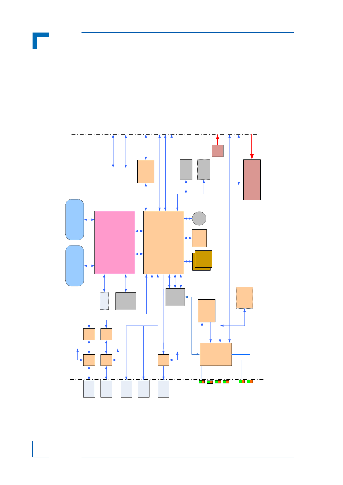
1.1 Board Overview
The CP3003-SA is a highly integrated 3U, 4 HP CompactPCI system controller board optionally
expandable to 8 HP and available either as a front I/O version or as a rear I/O version. It has
been designed to support the multi-chip package, 3
combined with the mobile Intel® QM77 Express Chipset.
The board supports the Intel® Core™ i7-3612QE quad-core processo r with 2.1 GHz frequency ,
the Intel® Core™ i7-3555LE dual-core processor with 2.5 GHz frequency and the Intel®
Core™ i7-3517UE dual-core processor with 1.7 GHz frequency . All processors are built on 22nm technology and provided in a BGA package. The processor is soldered on the CP3003-SA,
which results in a higher Mean Time Between Failures (MTBF) and a significant improvement
in cooling.
Two SODIMM sockets are available on the CP3003-SA to provide up to 16 GB dual-channel,
DDR3 memory with Error Checking and Correction (ECC) running at 1600 MHz. The graphics
controller and the memory controller are integrated in the processor. Furthermore, an external
HDD/SSD and either a SATA Flash module with up to 32 GB SLC NAND flash memory or a
Smart Extension Module (a SATA/USB 2.0 adapter) can be integrated onto the CP3003-SA.
rd
generation Intel® Core™ i7 processor
The CP3003-SA comes with three Gigabit Ethernet ports, one VGA interface, t wo COM p orts,
six SA TA interfaces, four USB 2.0 ports, one USB 3.0 port, two DisplayPort interfaces, and one
x8 PCI Express 2.0 XMC interface. The CP3003-SA provides support for one 8 HP I/O extension module such as the CP3003-HDD or the CP3003-XMC as well as one rear I/O module
such as the CP-RIO3-04.
The board supports a configurable 32-bit/ 33 MHz (66 MHz on request) PCI/PCI-X hot swap
CompactPCI interface. When installed in the system slot, the interface is enabled, and when
installed in a peripheral slot, the CP3003-SA is isolated from the CompactPCI bus.
The CP3003-SA further provides safety and security features via a Trusted Platform Module
(TPM) 1.2.
The board fits into all applications situated in industrial environments, including I/O intensive
applications where only one slot is available for the CPU, making it a perfect core technology
for long-life applications. Components which have high temperature tolerance have been
selected from embedded technology programs, and therefore offer long-term availability.
The board is offered with various Board Support Packages including Windows, VxWorks and
Linux operating systems. For further information concerning the operating systems available for
the CP3003-SA
,
please contact Kontron.
1.2 Board-Specific Information
The CP3003-SA is a CompactPCI single-board computer based on the 3rd generation Intel®
Core™ i7 processor and specifically designed for use in highly integrated platforms with solid
mechanical interfacing for a wide range of industrial environment applications.
D R A F T — F O R I N T E R N A L U S E O N L Y
ID 1052-6929, Rev. 2.0 Page 1 - 3
Page 24

Introduction CP3003-SA
Some of the CP3003-SA's outstanding features include:
• Support for the following 3
Intel® Core™ i7-3612QE (SV) quad-core processor, 2.1 GHz, 6 MB L3 cache
•
• Intel® Core™ i7-3555LE (LV)
Intel® Core™ i7-3517UE (ULV) dual-core processor, 1.7 GHz, 4 MB L3 cache
•
• Intel® QM77 Express Chipset
• Up to 16 GB, dual-channel, DDR3 SDRAM memory with ECC running at 1600 MHz on two
SODIMM sockets
• Integrated 3D high-performance processor graphics controller with up to three high-resolution graphics interfaces (1x VGA and 2 x DP)
• Digital display support for resolutions up to 2560 x 1600 pixels @ 60 Hz
• Analog display support for resolutions up to 2048 x 1536 pixels @ 75 Hz
• Three Gigabit Ethernet interfaces based on three Intel® 82574L controllers:
• Two interfaces switchable between front I/O and rear I/O (wit h Wake-on-LAN support)
• One interface available on the CP3003-HDD extension module (8HP)
• Six SATA interfaces with SATA RAID 0/1/5/10 support:
• One SATA 6 Gb/s interface for one external, standard HDD/SSD
• One SATA 3 Gb/s interface for up to 32 GB SLC NAND flash memory via an optional
SATA Flash module
• One SATA 3 Gb/s interface for one CFast memory card (8 HP with CP3003-HDD/
CP3003-XMC) or one SATA 2.5" HDD/SSD (12 HP)
• One SATA 6 Gb/s interface for one SATA 2.5" HDD/SSD (8 HP with CP3003-HDD)
• Two SATA 3 Gb/s interfaces for rear I/O
• Five USB ports:
• Two USB 2.0 ports on front I/O
• Two USB 2.0 ports on rear I/O
• One USB 3.0 port on the 120-pin onboard high-speed I/O extension connector
• Two D i sp l a y P o r t in t e r f a c es a v a i l a b le o n t h e CP3003-HDD extension module
• One x8 PCI Express 2.0 XMC interface available on the CP3003-XMC ex. module
• 32-bit/ 33 MHz PCI/PCI-X hot swap CompactPCI interface (PICMG 2.0); 66 MHz on request
• Compatible with CompactPCI Specification PICMG 2.0 Rev . 3.0 and usable in the system
controller slot as well as in a peripheral slot (the PCI interface is isolated in peripheral slot)
• TCG 1.2-compliant Trusted Platform Module (TPM)
• Two SPI boot flashes for two separate uEFI BIOS images:
• One standard SPI boot flash
• One recovery SPI boot flash
• Watchdog timer
• Battery-backed real-time clock (RTC)
• One onboard DIP switch for board configuration
•Two COM ports:
• COMA (RS-232) either on the 8 HP extension module or on the rear I/O
• COMB (RS-232) on the rear I/O
• Peripheral extension connectors:
• 120-pin high-speed I/O extension connector for 8 HP extension
D R A F T — F O R I N T E R N A L U S E O N L Y
• 60-pin high-speed PCI Express extension connector for 8 HP extension
• SPI extension connector
• Rear I/O on the CompactPCI connector J2
• 4 HP or 8 HP, 3U CompactPCI (12 HP on request)
• Several rear I/O configurations
• Power-up sequencing and in-rush current optimized design
• Passive heat sink solution for forced airflow cooling
• AMI Aptio®, a uEFI-compliant platform firmware
rd
generation processors:
dual-core processor
, 2.5 GHz, 4 MB L3 cache
Page 1 - 4 ID 1052-6929, Rev. 2.0
Page 25

CP3003-SA Introduction
1.3 System Expansion Capabilities
1.3.1 CP3003-HDD Module (8 HP and 12 HP)
The CP3003-HDD module for the 8 HP CP3003-SA version provides various I/O ports. On the
front panel, it includes two DisplayPort connectors, one Gigabit Ethernet port, one USB 3.0
port, and one RS-232 COM port. Onboard ports include one SATA connector for SATA 2.5”
HDD or SSD devices as well as a CFast card socket.
As a further extension capability of the CP3003-SA to 12 HP, a SATA adapter module is available for use in conjunction with the CP3003-HDD module to provide an additional SATA connector for a 2.5" SATA HDD/ SSD device. The 12 HP CP3003-SA does not provide a CFast
card socket.
For further information concerning the CP3003-HDD module, refer to Appendix A.
1.3.2 CP3003-XMC Module (8 HP)
The CP3003-XMC module for the 8 HP CP3003-SA version provides one XMC mezzanine interface for support of one x8, x4 or x1 PCI Express 2.0 XMC module. In addition, the CP3003XMC module provides a socket for CFast memory cards.
For further information concerning the CP3003-XMC module, refer to Appendix B.
1.3.3 CP-RIO3-04 Rear I/O Module
The CP-RIO3-04 rear I/O module has been designed for use with the CP3003-SA board from
Kontron and provides comprehensive rear I/O functionality.
For further information concerning the CP-RIO3-04 rear I/O module, refer to Appendix C.
1.3.4 SATA Flash Module
The 4 HP CP3003-SA provides support for up to 32 GB of SLC NAND flash memory in combination with an optional SATA Flash module, which is connected to an onboard connector.
For further information concerning the SATA Flash module, refer to Appendix D.
1.3.5 Smart Extension Module
The Smart Extension Module expands the onboard I/O capability and provides one additional
SATA cable connector as well as one USB 2.0 connector thereby facilitating the connection to
system-internal USB and SATA devices.
For further information concerning the SATA Flash module, refer to Appendix E.
1.4 Board Diagrams
The following diagrams provide additional information concerning board functionality and
component layout.
ID 1052-6929, Rev. 2.0 Page 1 - 5
D R A F T — F O R I N T E R N A L U S E O N L Y
Page 26
Introduction CP3003-SA
DDR3 / DDR3L w ECC
Bank B
SODIMM
DDR3 / DDR3L w ECC
Bank A
SODIMM
COMA & COMB (TTL)
Intel®
QM77
Front Panel
POST Code /
Debug /
Gen. Purpose
LEDs
CPLD
CompactPCI
Connector
COMA + COMB or
COMA + GPIO
Debug
3.3V and 5V
3
rd
gen.
Intel® Core™ i7
DDR3 DDR3
DMI
USB
DMI
LPC SMBusSPI
USB
SATA
USB 2.0
Type A
PCIe
FDI
FDI
VGA
CRT
VGA CRT
USB
2x SATA 3 Gb/s
2x SATA 3 Gb/s
GbE
GbE
RJ-45
RJ-45
TPM
PCIe
LPC
USB 2.0
Type A
DSUB
15-pin
USB
GbE
Contr.
GbE
Contr.
PCI
PCI 32-bit / 33MHz
3.3V / 5V VIO
2x USB 2.0
2x USB 2.0
GbE
PCIe
PCIe x1
High-
Speed
I/O
Extension
C
onnector
SATA, PCIe, HDA, USB 3.0
DP
SATA
2x SATA
PCIe x1
2x USB 2.0
VGA CRT
VGA
PM
VGA CRT
Power Management
GbE
Watchdog /
Thermal
LEDs
COMA
Onboard Power Supplies
DC/DC etc.
USB
Power
2x USB Power
GbE
Switch
GbE
Switch
Rear I/O Eth
Rear I/O Eth
Rear I/O Eth
Rear I/O Eth
SFF XDP
EEPROM
Bat.
RTC
SATA
7-pin
Connector
SATA
Flash
Module
PCI
Bridge
PCIe x1
VGA
Mux
To Rear I/O
High-
Speed
PCIe
Extension
C
onnector
PCIe
PCIe x8
SATA 6 Gb/s
Dual
UART
COMA+B
XBUS
SPI Boot
Flashes
(standard/
recovery)
(optional)
1.4.1 Functional Block Diagram
Figure 1-1: CP3003-SA Functional Block Diagram
D R A F T — F O R I N T E R N A L U S E O N L Y
Page 1 - 6 ID 1052-6929, Rev. 2.0
Page 27
CP3003-SA Introduction
USB 2.0
CP3003
GbE A
GbE B
Watchdog and Overtemperature Status LEDs
WD (green): Watchdog Status
TH (red/green): Overtemperature Status
Integral Ethernet LEDs
ACT (green): Ethernet Link/Activity
SPEED (green/orange/off): Ethernet Speed
General Purpose LEDs
LED0..3 (red/green/red+green): General Purpose/POST Code
Note ...
If the General Purpose LEDs 0..3 are lit red during
boot-up, a failure is indicated before the uEFI BIOS
has started.
1.4.2 Front Panel
Figure 1-2: 4 HP CP3003-SA Front Panel
Note ...
D R A F T — F O R I N T E R N A L U S E O N L Y
For information regarding the front panel of the 8 HP or 12 HP CP3003-SA with
a CP3003-HDD module, refer to Appendix A, CP3003-HDD Module.
For information regarding the front panel of the 8 HP CP3003-SA with a
CP3003-XMC module, refer to Appendix B, CP3003-XMC Module.
ID 1052-6929, Rev. 2.0 Page 1 - 7
Page 28

Introduction CP3003-SA
1
SATA
Flash
Module
Smart
Extension
Module
J11
J4
VGA
J5
USB
J6
USB
J7A
GbE A
J7B
GbE B
J2
J1
Intel® QM77
DDR3 SODIMM Sockets
J3
J13
Intel® Core™i7
J14
Ch. A
Memory
Modules
Ch. B
J12
1
1
2
2
13
14
17
18
1
2
9
10
J8
P
r
o
ce
ssor
Chipset
J15
LED 0
LED 1
LED 2
LED 3
TH LED
WD LED
ON
SW1
J2
J1
1.4.3 Board Layout
Figure 1-3: 4 HP CP3003-SA Board Layout (Top View)
Figure 1-4: 4 HP CP3003-SA Board Layout (Bottom View)
D R A F T — F O R I N T E R N A L U S E O N L Y
Page 1 - 8 ID 1052-6929, Rev. 2.0
Page 29

CP3003-SA Introduction
1.5 Technical Specification
Table 1-1: CP3003-SA Main Specifications
FEATURES SPECIFICATIONS
CPU
Memory
Processor and Memory
Intel® QM77
Chipset
rd
The CP3003-SA supports the following 3
generation microprocessors:
• Quad-core Intel® Core™ i7-3612QE (SV), 2.1 GHz, 6 MB L3 cache
• Dual-core Intel® Core™ i7-3555LE (LV), 2.5 GHz, 4 MB L3 cache
• Dual-core Intel® Core™ i7-3517UE (ULV), 1.7 GHz, 4 MB L3 cache
Further processor features used on the CP3003-SA:
• Up to four execution cores
• Intel® Hyper-Threading Technology (Intel® HT Technology)
• Intel® 64 Architecture
• Intel® Advanced Vector Extensions (AVX) floating point
• Intel® Turbo Boost Technology
• System memory interface with optimized support for dual-channel
DDR3 SDRAM memory at 1600 MHz with ECC
• Integrated 2D and 3D Graphics Engines
• DMI 2.0 with 5 GT/s and FDI interfaces to the Intel® QM77 Chipset
• One x8 PCI Express 2.0 port operating at 5 GT/s
Please contact Kontron for further information concerning the suitability of
other Intel processors for use with the CP3003-SA.
Main Memory:
• Up to 16 GB, dual-channel DDR3 SDRAM memory with ECC running at
1600 MHz on two SODIMM sockets
Cache Structure:
• 64 kB L1 cache for each core
• 32 kB instruction cache
• 32 kB data cache
• 256 kB L2 shared instruction/data cache for each core
• Up to 6 MB L3 shared instruction/data cache shared between all cores
Flash Memory:
• Two SPI boot flash chips (2 x 8 MB) for two separate uEFI BIOS images
• Up to 32 GB SLC NAND flash via an onboard SAT A Flash module (SSD)
Serial EEPROM with 64 kbit
Mobile Intel® QM77 Express Chipset features used on the CP3003-SA:
• Four x1 PCI Express 2.0 ports operating at 5 GT/s
• SATA host controller with six ports and RAID 0/1/5/10 support
• Two SATA 6 Gb/s ports
• Four SATA 3 Gb/s ports
• Four USB 2.0 host interfaces and up to two USB 3.0 host interfaces
• Integrated Ethernet controller
• SPI flash interface support
• Low Pin Count (LPC) interface
• Power management logic support
• Enhanced DMA controller, interrupt controller, and timer functions
• System Management Bus (SMBus) compatible with most I²C™ devices
• DMI 2.0 with 5 GT/s and FDI interfaces to the processor
• Analog display port
• Two digital display ports
• High Definition Audio interface
• Integrated RTC
D R A F T — F O R I N T E R N A L U S E O N L Y
ID 1052-6929, Rev. 2.0 Page 1 - 9
Page 30

Introduction CP3003-SA
Table 1-1: CP3003-SA Main Specifications (Continued)
FEATURES SPECIFICATIONS
Graphics Controller High-performance 3D graphics controller integrated in the processor:
• Dynamic Video Memory Technology (DVMT)
• Supports digital displays with resolutions up t o 2560 x 1600 pixels @
60 Hz through DisplayPort or up to 1920x1200 pixels @ 60Hz using
HDMI/DVI. HDMI/DVI displays are supported via an appropriate
Controller
Integrated
CompactPCI Compliant with CompactPCI Specification PICMG® 2.0 R 3.0:
adapter. Refer to Chapter 2.11.4, Table 2-8 for further information on
the display configuration options.
• Supports analog display with resolutions up to 2048 x 1536 pixels @
75 Hz for VGA displays
• System master operation
• 32-bit/33 MHz master interface (66 MHz on request)
• 3.3 V or 5 V (universal PCI interface)
• Support for up to seven peripheral slots (7x REQ/GNT signals)
When installed in a peripheral slot, the CP3003-SA is isolated from the CompactPCI bus. It receives power from the backplane and supports rear I/O.
CP3003-SA removal under power:
When installed in a peripheral slot, the CP3003-SA supports hot plugging
on the power interface through a dedicated power controller, but not on the
PCI interface.
Hot swapping of peripheral boards controlled by the CP3003-SA:
When installed in the system controller slot, the CP3003-SA supports the hot
swapping of other boards. Individual clocks for each slot and Enum signal
Interfaces
Rear I/O The following interfaces are routed to the rear I/O connector J2:
handling are in compliance with the PICMG 2.1 Hot Swap Specification.
The CP3003-SA itself, however, is not hot swappable. When installed in the
system controller slot, the system must be powered down in order to replace
the board.
• COMA and COMB, or COMA and GPIO (all ports have 3.3V LVTTL sig-
naling)
• 2 x USB 2.0
• VGA (analog)
• 2x Gigabit Ethernet
• 2x SATA 3Gb/s
• System management signals
• Input for 5V standby power
• General purpose signals
D R A F T — F O R I N T E R N A L U S E O N L Y
Page 1 - 10 ID 1052-6929, Rev. 2.0
Page 31
CP3003-SA Introduction
Table 1-1: CP3003-SA Main Specifications (Continued)
FEATURES SPECIFICATIONS
Gigabit Ethernet Three 10 Base-T/100 Base-TX/1000 Base-T Gigabit Ethernet interfaces based
on three Intel® 82574L Ethernet PCI Express bus controllers, two interfaces
individually switchable to front I/O or rear I/O, on e interface ava ilable on the
CP3003-HDD module:
• Dual RJ-45 connector on the front panel
• Automatic mode recognition (Auto-Negotiation)
• Automatic cabling configuration recognition (Auto-MDI/X)
• Wake-on-LAN support available only on the two interfaces switch-
able to front I/O or rear I/O
USB Five USB ports:
• Two USB 2.0 ports on the front I/O
• Two USB 2.0 ports on the rear I/O interface
• One USB 3.0 port on the 120-pin onboard high-speed I/O extension con-
nector
Serial Two 16C550-compatible UARTs:
• COMA available on the 8 HP extension module or on rear I/O
• COMB or GPIO available on rear I/O only
SATA
I/O Expansion
Interfaces
Interfaces
• Six SATA ports, two onboard, two on rear I/O, and two on the 8 HP ex-
tension module
• Data transfer rates up to 600 MB/s
• High-performance RAID 0/1/5/10 functionality on all SATA ports
I/O expansion to 8 HP board version via the CP3003-HDD module:
• SATA 6 Gb/s
• CFast (SATA 3 Gb/s)
• USB 3.0
• 2x DP (DisplayPort)
• COMA
• Reset button and HDD/SSD activity LED
• Gigabit Ethernet
I/O expansion to 12 HP board version via the CP3003-HDD module and the
2.5" SATA adapter module:
• 2x SATA (SATA 3 Gb/s and SATA 6 Gb/s)
• USB 3.0
• 2x DP (DisplayPort)
• COMA
• Reset button and HDD/SSD activity LED
• Gigabit Ethernet
I/O expansion to 8 HP board version via the CP3003-XMC module:
• PCI Express x8, x4 or x1
• CFast (SATA 3 Gb/s)
I/O expansion of CP3003-SA via the Smart Extension Module (exceeds 4 HP):
• SATA 3 Gb/s
• USB 2.0
ID 1052-6929, Rev. 2.0 Page 1 - 11
D R A F T — F O R I N T E R N A L U S E O N L Y
Page 32

Introduction CP3003-SA
Table 1-1: CP3003-SA Main Specifications (Continued)
FEATURES SPECIFICATIONS
Front Panel Connectors
• VGA: 15-pin D-Sub connector, J4
• USB: two 4-pin, type A connectors, J5 and J6
• Ethernet: dual RJ-45 connector, J7A/B
Onboard Connectors
• 7-pin, L-form standard SATA connector, J3
• 120-pin, high-speed I/O extension connector, J14
• 60-pin, high-speed PCI Express extensio n connector, J8
Sockets
• SPI extension connector, J11
• 18-pin extension connector for the SATA Flash module (SSD), J12
• JTAG connector, J13
• XDP-SFF (debug) connector, J15
• CompactPCI connectors J1 and J2
• Two 204-pin DDR3 SODIMM sockets
DIP Switch One DIP switch, SW1, for board configuration
Switch
LEDs Watchdog and Overtemperature Status LEDs:
• WD (green): Watchdog Status
• TH (red/green): Overtemperature Status
General Purpose LEDs:
LEDs
• LED0..3 (red/green/red+green): General Purpose/POST Code
Ethernet LEDs:
• ACT (green): Network/Link Activity
• SPEED (green/orange): Network Speed
Watchdog Timer
• Software-configurable, two-stage Watchdog with programmable timeout
ranging from 125 ms to 4096 s in 16 steps
• Serves for generating IRQ or hardware reset
System Timer
Timer
Thermal Management
• The Intel® QM77 Chipset contains three 8254-style counters which
have fixed uses
• In addition to the three 8254-style counters, the Intel® QM77 Chipset in-
cludes eight individual high-precision event timers that may be used by
the operating system. They are implemented as a single counter each
with its own comparator and value register.
CPU and board overtemperature protection is provided by:
• Up to four Digital Thermal Sensors (DTS), one for each core
• One Digital Thermal Sensor (DTS) for the processor graphics controller
• One temperature sensor integrated in the Intel® QM77 Chipset for
monitoring the chipset
Sys. Management
TPM Trusted Platform Module (TPM) 1.2 for enhanced hardware- and software-
D R A F T — F O R I N T E R N A L U S E O N L Y
Security
• Specially designed heat sinks
based data and system security
Page 1 - 12 ID 1052-6929, Rev. 2.0
Page 33

CP3003-SA Introduction
Note ...
When a battery is installed, refer to the operational specifications
of the battery as this determines the storage temperature of the
CP3003-SA (See "Battery" below).
Note ...
When additional components are installed, refer to their operational specifications as this will influence the operational and storage temperature of the CP3003-SA.
Note ...
If a Smart Extension Module is installed on the CP3003-SA, the
board exceeds 4 HP.
Table 1-1: CP3003-SA Main Specifications (Continued)
FEATURES SPECIFICATIONS
uEFI BIOS AMI Aptio®, AMI’s next-generation BIOS firmware based on the uEFI Specifi-
cation and the Intel Platform Innovation Framework for EFI.
• LAN boot capability for diskless systems (standard PXE)
• Redundant image; fail-safe recovery in case of a damaged image
• Non-volatile storage of setting in the SPI boot flash (battery only re-
quired for the RTC)
• Compatibility Support Module (CSM) providing legacy BIOS compatibil-
Software
Operating Systems
Mechanical 3U, 4 HP, CompactPCI-compliant form factor
Power Consumption See Chapter 5 for details.
Temperature Range
ity based on AMIBIOS8
• Command shell for diagnostics and configuration
• EFI shell commands executable from mass storage device in a Pre-OS
environment (open interface)
There are various operating systems available for the CP3003-SA. For
detailed information, please contact Kontron.
Operational: 0°C to +60°C Standard (depending on processor version
and airflow in the system)
-40°C to +85°C Extended (with Intel® Core™ i7-3517UE,
1.7 GHz ULV processor only)
Storage: -40°C to +85°C Without hard disk and without battery
Battery 3.0V lithium battery for RTC with battery socket.
General
Battery type: UL-approved CR2025
Temperature ranges:
Operational (load): -20°C to +70°C typical (refer to the battery manufac-
turer’s specifications for exact range)
Storage (no load): -55°C to +70°C typical (no discharge)
Climatic Humidity
Dimensions
Board Weight
ID 1052-6929, Rev. 2.0 Page 1 - 13
Note ...
For a description of the additional 8 HP version interfaces, refer to Appendix A,
CP3003-HDD Module and Appendix B, CP3003-XMC Module.
93% RH at 40 °C, non-condensing (acc. to IEC 60068-2-78)
100 mm x 160 mm
313 grams (4 HP CP3003-SA with heat sink, front panel, two 2 GB SODIMM
memory modules, and battery but without SATA Flash module or without
Smart Extension Module respectively)
D R A F T — F O R I N T E R N A L U S E O N L Y
Page 34

Introduction CP3003-SA
1.6 Standards
This product complies with the requirements of the following standards.
Table 1-2: Standards
TYPE ASPECT STANDARD
CE Emission EN55022
EN61000-6-3
Immission EN55024
EN61000-6-2
Electrical Safety EN60950-1
Mechanical Mechanical Dimensions IEEE 1101.10
Environmental Climatic Humidity IEC60068-2-78
(see note below)
WEEE Directive 2002/96/EC
Waste electrical and electronic equipment
RoHS 2 Directive 2011/65/EU
Restriction of the use of certain hazardous substances in electrical and electronic equipment
Note ...
Kontron performs comprehensive environmental testing of its products in accordance with applicable standards.
Customers desiring to perform further environmental testing of Kontron products must contact Kontron for assistance prior to performing any such testing.
This is necessary, as it is possible that environmental testing can be destructive
when not performed in accordance with the applicable specifications.
In particular, for example, boards without conformal coating must not be
exposed to a change of temperature exceeding 1K/minute, averaged over a
period of not more than five minutes. Otherwise, condensation may cause irreversible damage, especially when the board is powered up again.
Kontron does not accept any responsibility for damage to products resulting
from destructive environmental testing.
D R A F T — F O R I N T E R N A L U S E O N L Y
Page 1 - 14 ID 1052-6929, Rev. 2.0
Page 35

CP3003-SA Introduction
In addition, boards ordered with the ruggedized service comply with the following standards as well.
Table 1-3: Additional Standards for Boards Ordered with Ruggedized Service
TYPE ASPECT STANDARD REMARKS
Environmental Vibration
(Sinusoidal)
Single Shock IEC60068-2-27 Ruggedized version test parameters:
Permanent Shock IEC60068-2-29 Ruggedized version test parameters:
IEC60068-2-6 Ruggedized version test parameters:
• 10-300 (Hz) frequency range
• 5 (g) acceleration
• 1 (oct/min) sweep rate
• 10 cycles/axis
•3 axis
• 30 (g) acceleration
• 9 (ms) shock duration half sine
• 3 number of shocks per direction (total: 18)
• 6 directions
• 5 (s) recovery time
• 15 (g) acceleration
• 11 (ms) shock duration half sine
• 500 number of shocks per direction
• 6 directions
• 5 (s) recovery time
1.7 Related Publications
The following publications contain information relating to this product.
Table 1-4: Related Publications
PRODUCT PUBLICATION
CompactPCI Systems CompactPCI Specification PICMG 2.0, Rev. 3.0
CompactPCI Hot Swap Specification PICMG 2.1 Rev. 2.0
SATA Serial ATA 1.0a Specification
CFast CFast Specification Revision 1.0
XMC ANSI/VITA 42.0-200x XMC Switched Mezzanine Card Auxiliary Standard
ANSI/VITA 42.3-2006 XMC PCI Express Protocol Layer Standard
DisplayPort VESA DisplayPort Standard Version 1.1a
Platform Firmware Unified Extensible Firmware Interface (uEFI) specification, version 2.1
All Kontron products Product Safety and Implementation Guide, ID 1021-9142
D R A F T — F O R I N T E R N A L U S E O N L Y
ID 1052-6929, Rev. 2.0 Page 1 - 15
Page 36

Introduction CP3003-SA
This page has been intentionally left blank.
D R A F T — F O R I N T E R N A L U S E O N L Y
Page 1 - 16 ID 1052-6929, Rev. 2.0
 Loading...