

Page 1

USERS MANUAL
Revision 4.0 MTD/PS-0521
December 1, 2005
KODAK KAI-4011 / KAI-4021 IMAGER EVALUATION BOARD
Page 2

TABLE OF CONTENTS
Description ..................................................................................................................................................................................3
Input Requirements ....................................................................................................................................................................3
Architecture Overview .................................................................................................................................................................4
Power Filtering And Regulation..................................................................................................................................................4
LVDS Receivers / TTL Buffers.....................................................................................................................................................4
CCD Pixel-Rate Clock Drivers (H1, H2 & Reset Clocks)............................................................................................................4
Reset Clock One-Shot (U15; not populated) ..............................................................................................................................4
CCD VCLK Drivers.......................................................................................................................................................................4
CCD FDG DRIVER........................................................................................................................................................................4
VES CIRCUIT................................................................................................................................................................................4
CCD Bias Voltages.......................................................................................................................................................................4
CCD Image Sensor......................................................................................................................................................................4
Emitter-Follower.........................................................................................................................................................................4
Line Drivers .................................................................................................................................................................................4
Operational Settings ...................................................................................................................................................................5
Bias Voltages...............................................................................................................................................................................5
Clock Voltages.............................................................................................................................................................................5
Block Diagram and Performance Data ......................................................................................................................................6
Connector Assignments and Pinouts .........................................................................................................................................8
SMB Connectors J2 and J3 .........................................................................................................................................................8
Board Interface Connector J1 ....................................................................................................................................................8
Warnings and Advisories.............................................................................................................................................................9
Glossary of Abbreviations ...........................................................................................................................................................9
Revision History ..........................................................................................................................................................................9
Appendices................................................................................................................................................................................ 10
KAI-4011/KAI-4021 Imager Board Schematics........................................................................................................................10
TABLES
Table 1: Power Requirements........................................................................................................................................................3
Table 2: Signal Level Requirements ..............................................................................................................................................3
Table 3: Bias Voltages..................................................................................................................................................................... 5
Table 4: Clock Voltages...................................................................................................................................................................5
Table 5: J1 Interface Connector Pin Assignments ........................................................................................................................8
FIGURES
Figure 1: KAI-4011/KAI-4021 Imager Board Block Diagram........................................................................................................6
Figure 2: Measured Performance -- Linearity ..............................................................................................................................7
Figure 3: Measured Performance -- Dynamic Range and Noise Floor........................................................................................7
©Eastman Kodak Company, 2005 www.kodak.com/go/imagers Revision 4.0 (MTD/PS-0521) p2
Page 3
DESCRIPTION
The KAI-4011/KAI-4021 Imager Evaluation Board,
referred to in this document as the Imager Board, is
designed to be used as part of a two-board set, used in
conjunction with a Timing Generator Board. Kodak
offers an Imager Board / Timing Generator Board
package that has been designed and configured to
operate with the KAI-4011/KAI-4021 CCD image sensors.
The Timing Generator Board generates the timing
signals necessary to operate the CCD, and provides the
power required by the Imager Board. The timing signals,
in LVDS format, and the power, are provided to the
Imager Board via the interface connector (J1). In
addition, the Timing Generator Board performs the
processing and digitization of the analog video output of
the Imager Board.
The KAI-4011/KAI-4021 Imager Board has been designed
to operate the KAI-4011/KAI-4021 CCDs with the
specified performance at 40MHz pixel clocking rate and
nominal operating conditions. (See the KAI-4011/KAI4021 performance specifications for details).
For testing and characterization purposes, the KAI4011/KAI-4021 Imager board provides the ability to adjust
many of the CCD bias voltages and CCD clock level
voltages by adjusting potentiometers on the board. The
Imager Board provides the means to modify other device
operating parameters (CCD reset clock pulse width, VSS
bias voltage) by populating components differently on the
board.
INPUT REQUIREMENTS
Input Signals (LVDS) Vmin Vthreshold Vmax Units Comments
H1A (+/-) 0 +/- 0.1 2.4 V H1A clock
H1B (+/-) 0 +/- 0.1 2.4 V H1B clock
H2A (+/-) 0 +/- 0.1 2.4 V H2A clock
H2B (+/-) 0 +/- 0.1 2.4 V H2B clock
FDG 0 +/- 0.1 2.4 V Fast Dump clock
R (+/-) 0 +/- 0.1 2.4 V Reset clock
V1 (+/-) 0 +/- 0.1 2.4 V V1 clock
V2 (+/-) 0 +/- 0.1 2.4 V V2 clock
V2B(+/-) 0 +/- 0.1 2.4 V V2B clock
V3RD (+/-) 0 +/- 0.1 2.4 V V2 Clock 3rd-level
VES (+/-) 0 +/- 0.1 2.4 V Electronic Shutter
AMP_ENABLE (+/-) 0 +/- 0.1 2.4 V Output Amplifier Enable
Power Supplies Minimum Typical Maximum Units
4.9 5 5.1 V +5V_MTR Supply
1400 mA
-5.1 -5 -4.9 V -5V_MTR Supply
200 mA
18 20 21 V VPLUS Supply
175 mA
-21 -20 -18 V VMINUS Supply
150 mA
Table 1: Power Requirements
Table 2: Signal Level Requirements
©Eastman Kodak Company, 2005 www.kodak.com/go/imagers Revision 4.0 (MTD/PS-0521) p3
Page 4

ARCHITECTURE OVERVIEW
The following sections describe the functional blocks of the KAI-4011/KAI-4021 Imager board (refer to Figure 1).
once per frame to transfer the charge from the
POWER FILTERING AND REGULATION
Power is supplied to the Imager Board via the J1
interface connector. The power supplies are de-coupled
and filtered with ferrite beads and capacitors to suppress
noise. Voltage regulators are used to create the +15 and
–15V supplies from the VPLUS and VMINUS supplies.
LVDS RECEIVERS / TTL BUFFERS
LVDS timing signals are input to the Imager Board via
the J1 interface connector. These signals are shifted to
TTL levels before being sent to the CCD clock drivers.
photodiodes to the vertical CCDs.
CCD FDG DRIVER
The Fast Dump Gate (FDG) driver is a transistor that will
switch the voltage on the FDG pin of the CCD from
FDG_LOW to FDG_HIGH during Fast Dump Gate
operation. When not in operation, or when the Fast
Dump Gate feature is not being utilized, the FDG pin of
the CCD is held at FDG_LOW. The FDG_HIGH and
FDG_LOW voltage levels of the FDG driver are set by
resistor divider circuits, and are buffered by operational
amplifiers configured as voltage followers.
CCD PIXEL-RATE CLOCK DRIVERS (H1, H2 & RESET CLOCKS)
The pixel rate CCD clock drivers utilize two fast switching
transistors that are designed to translate TTL-level input
clock signals to the voltage levels required by the CCD.
The high level and low level of the CCD clocks are set by
potentiometers.
RESET CLOCK ONE-SHOT (U15; NOT
VES CIRCUIT
The quiescent CCD substrate voltage (VSUB) is set by a
potentiometer. For electronic shutter operation, the VES
signal drives a transistor amplifier circuit that ACcouples the voltage difference between the VPLUS and
VMINUS supplies onto the Substrate voltage. This
creates the necessary potential to clear all charge from
the photodiodes, thereby acting as an electronic shutter
to control exposure.
POPULATED)
The pulse width of the RESET_CCD clock used to be set
by a programmable One-Shot. The One-Shot was
configured to provide a RESET_CCD clock signal with a
pulse width from 5ns to 15ns. Now, the pulse width
control functionality is provided by the KSC-1000 Timing
Generator Board, and the one-shot has been bypassed by
removing U15 and inserting a shorting resistor on pads 1
and 2 of U15.
CCD VCLK DRIVERS
The vertical clock (VCLK) drivers consist of MOSFET
driver IC’s. These drivers are designed to translate the
TTL-level clock signals to the voltage levels required by
the CCD. The high, middle, and low voltage levels of the
vertical clocks are set by potentiometers buffered by
operational amplifiers configured as voltage followers.
The current sources for these voltage levels are high
current (up to 600 mA) transistors. The V2_CCD high
level clock voltage is switched from V_MID to V_HIGH
CCD BIAS VOLTAGES
The CCD bias voltages are set by potentiometers,
buffered by operational amplifiers configured as voltage
followers. The bias voltages are de-coupled at the CCD
pin.
CCD IMAGE SENSOR
This evaluation board supports the Kodak KAI-4011 and
KAI-4021 Interline CCD image sensors.
EMITTER-FOLLOWER
The VOUT_CCD signals are buffered using bipolar
junction transistors in the emitter-follower configuration.
These circuits also provide the necessary 5mA current
sink for the CCD output circuits.
LINE DRIVERS
The buffered VOUT_CCD signals are AC-coupled and
driven from the Imager Board by operational amplifiers
©Eastman Kodak Company, 2005 www.kodak.com/go/imagers Revision 4.0 (MTD/PS-0521) p4
Page 5

in a non-inverting configuration. The operational
amplifiers are configured to have a gain of 2, to correctly
drive 75Ω video coaxial cabling from the SMB
connectors.
OPERATIONAL SETTINGS
The Imager board is configured to operate the KAI-4011/KAI-4021 CCD image sensors under the following operating
conditions:
BIAS VOLTAGES
The following voltages are fixed, or adjusted with a potentiometer as noted. The nominal values listed in Table 3 were
correct at the time of this document’s publication, but may be subject to change; refer to the KAI-4011/KAI-4021 device
specification.
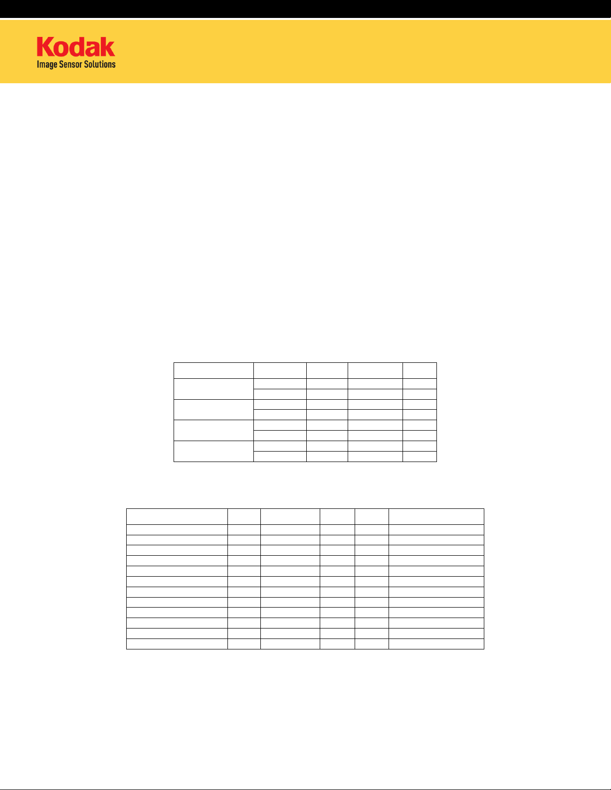
Description Symbol Min Nominal Max Units Potentiometer Notes
Left Output Amplifier Supply VDDL 15.0 V -
Right Output Amplifier Supply VDDR 15.0 V - 1
Reset Drain VRD 6.7 12.0 13.5 V R23 3
ESD Protection ESD -9.0 V -
Substrate VSUB 8.5 TBD 15.0 V R18 3
Output Gate Left VOGL -7.5 -3.5 -0.4 V R11 2,3
Output Gate Right VOGR -7.5 -3.5 -0.4 V R7 2,3
Table 3: Bias Voltages
NOTES:
1. If the CCD is to be operated in single output mode only (VOUT_LEFT) the unused output amplifier supply can be tied to ground to conserve
2. The Output Gate signals VOGL and VOGR may be controlled independently, or, by installing R28 and R33 and removing R29, may be set to
3. The Min and Max voltages in the table indicate the imager board potentiometer adjustable voltage range. These values may exceed the
power by not populating R71, R72 and C76 and by replacing C75 with a 0 ohm resistor.
the same potential, controlled by R11.
specified CCD operating conditions. See the KAI-4011/KAI-4021 device specification for details.
CLOCK VOLTAGES
The following clock voltage levels are fixed, or adjusted with a potentiometer as noted. The nominal values listed in Table
4 were correct at the time of this document’s publication, but may be subject to change; refer to the KAI-4011/KAI-4021
device specification.
Description Symbol Level Min Nom Max Unit Potentiometer Notes
Hxx_CCD Low -7.5 -4.5 -0.8 V R147 1 Horizontal CCD Clock
High 0.4 0.5 7.5 V R127 2
Vertical CCD Clock
NOTES:
1. The H1A_CCD, H1B_CCD, H2A_CCD, and H2B_CCD low levels are controlled by the same potentiometer (R147).
2. The H1A_CCD, H1B_CCD, H2A_CCD, and H2B_CCD high levels are controlled by the same potentiometer (R127).
3. V1_CCD and V2_CCD low levels are controlled by the same potentiometer (R40)
4. V1_CCD and V2_CCD mid levels are controlled by the same potentiometer (R66)
5. FDG is used to flush the device when operated in Still Mode.
©Eastman Kodak Company, 2005 www.kodak.com/go/imagers Revision 4.0 (MTD/PS-0521) p5
Vx_CCD Low -14.0 -9.0 -1.0 V R40 3
Vx_CCD Mid -2.5 -0.0 -0.0 V R66 4
V2_CCD High 4.0 9.0 11.0 V R48
RESET_CCD Low -7.0 -3.5 -1.0 V R20 Reset Clock
High 1.0 5.0 7.0 V R19
FDG_CCD Low -9.0 V 5 Fast Dump Clock
High 5.0 V
Table 4: Clock Voltages
Page 6
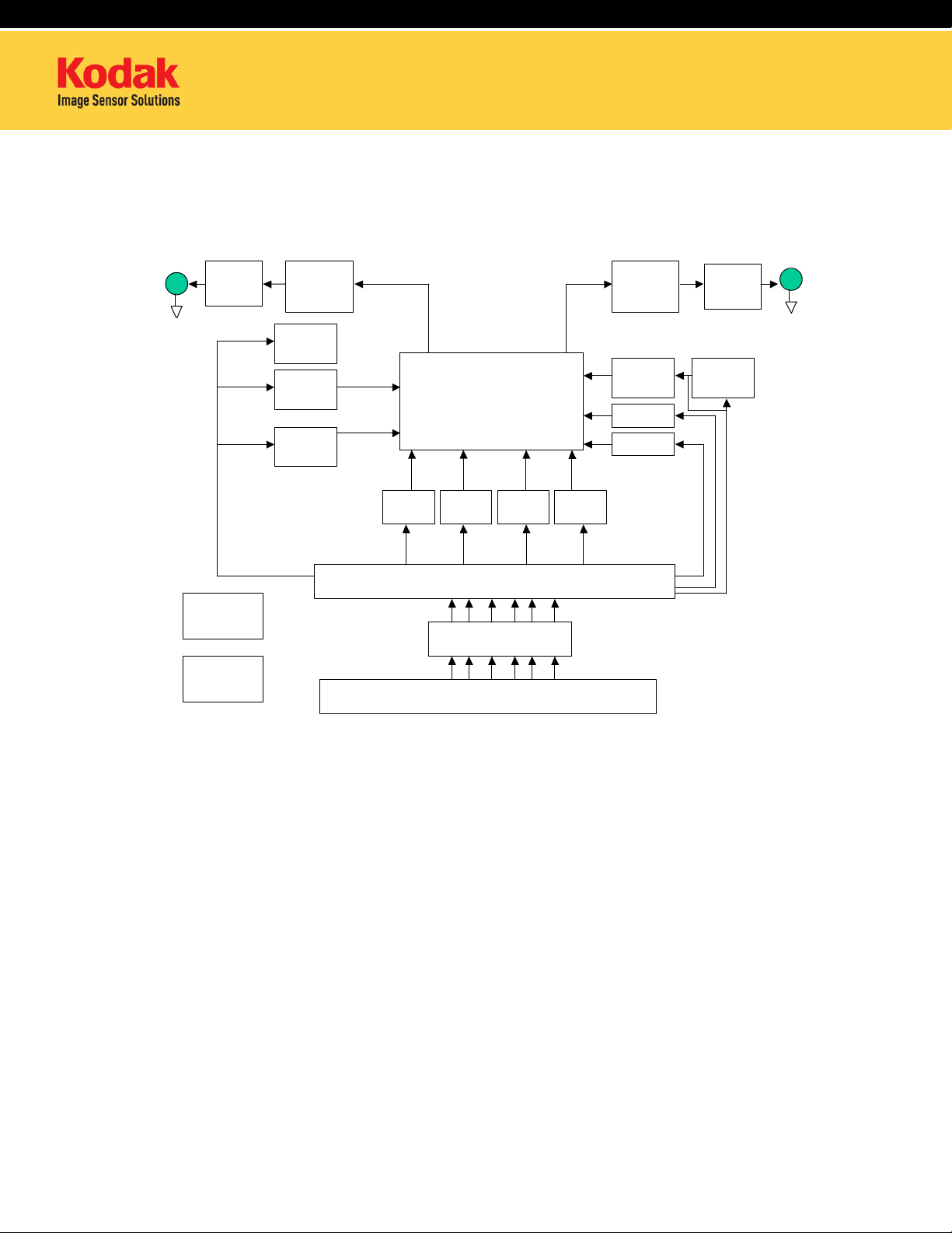
BLOCK DIAGRAM AND PERFORMANCE DATA
J3
SMB
+15V
REGULATOR
-15V
REGULATOR
LINE
DRIVER
EMITTER
FOLLOWER
V3RD
DRIVER
V2
DRIVER
V1
DRIVER
VOUT LEFT
H1A
DRIVER
CCD SENSOR
H2A
DRIVER
VOUT RIGHT
H1B
DRIVER
H2B
DRIVER
LVDS TO TTL BUFFERS
LVDS RECEIVERS
J1 BOARD INTERFACE CONNECTOR
EMITTER
FOLLOWER
RCLK
DRIVER
FDG CKT
VES CKT
LINE
DRIVER
(optional)
RCLK
1 SHOT
J2
SMB
Figure 1: KAI-4011/KAI-4021 Imager Board Block Diagram
©Eastman Kodak Company, 2005 www.kodak.com/go/imagers Revision 4.0 (MTD/PS-0521) p6
Page 7
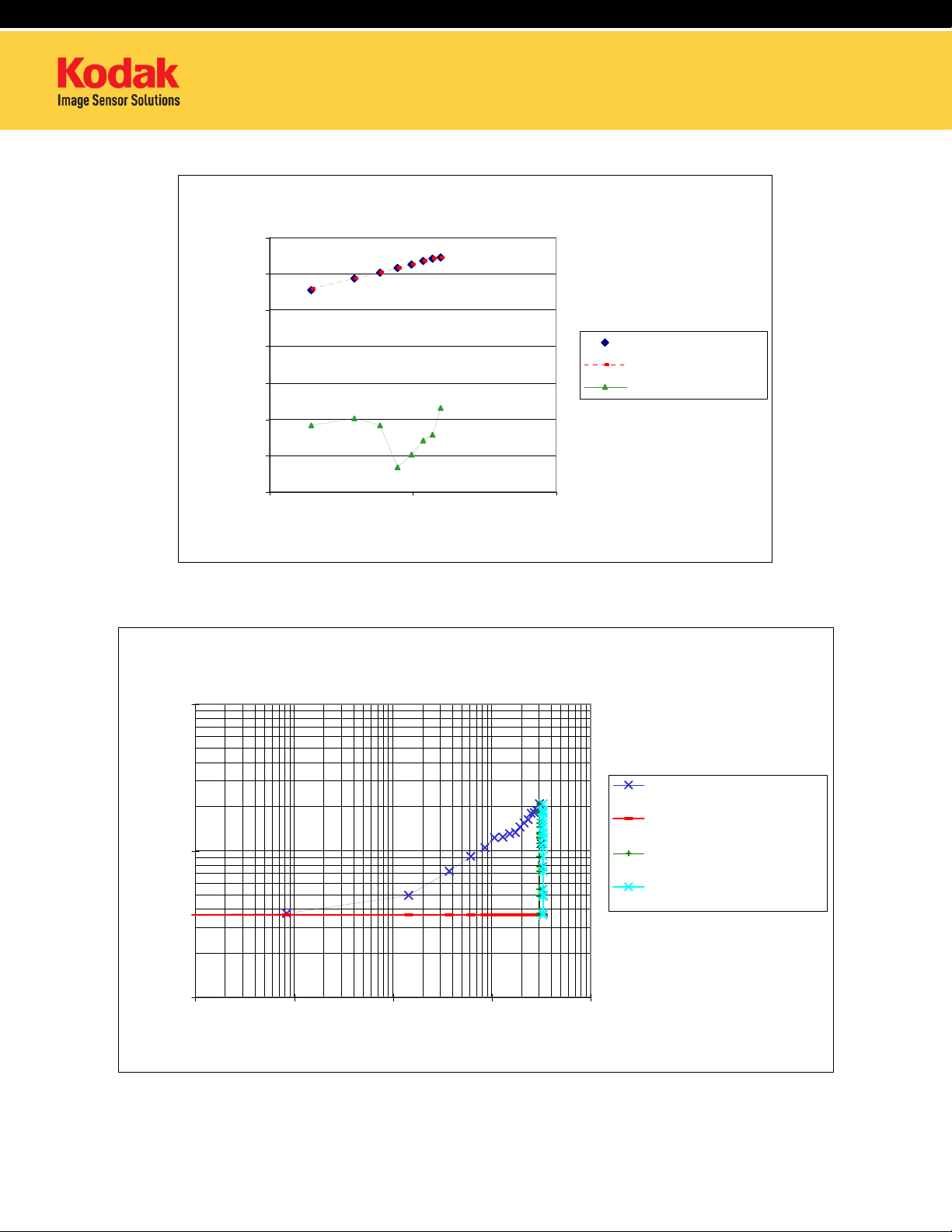
S
LINEARITY
100000
10000
1000
100
10
1
SIGNAL MEAN (ELECTRON
0.1
0.01
0.1 1 10
INTEGRATION TIME (SECONDS)
MEA SURED
FIT
%DEVIA TION FROM FIT
Figure 2: Measured Performance -- Linearity
Photon Transfer
100
Slope = el/Adu = 9.29 electrons
Noise floor = 3.65 counts (33.9
electrons)
10
LVSAT = 30220 electrons
VSAT = 32980 electrons
Noise (A/D counts)
1
10 100 1000 10000 100000
Signal Mean (Electrons)
Figure 3: Measured Performance -- Dynamic Range and Noise Floor
©Eastman Kodak Company, 2005 www.kodak.com/go/imagers Revision 4.0 (MTD/PS-0521) p7
Page 8
CONNECTOR ASSIGNMENTS AND PINOUTS
SMB CONNECTORS J2 AND J3
The emitter-follower buffered CCD_VOUT signals are driven from the Imager Board via the SMB connectors J2 and J3.
Coaxial cable with a characteristic impedance of 75 Ω should be used to connect the imager board to the Timing Generator
Board to match the series and terminating resistors used on these boards.
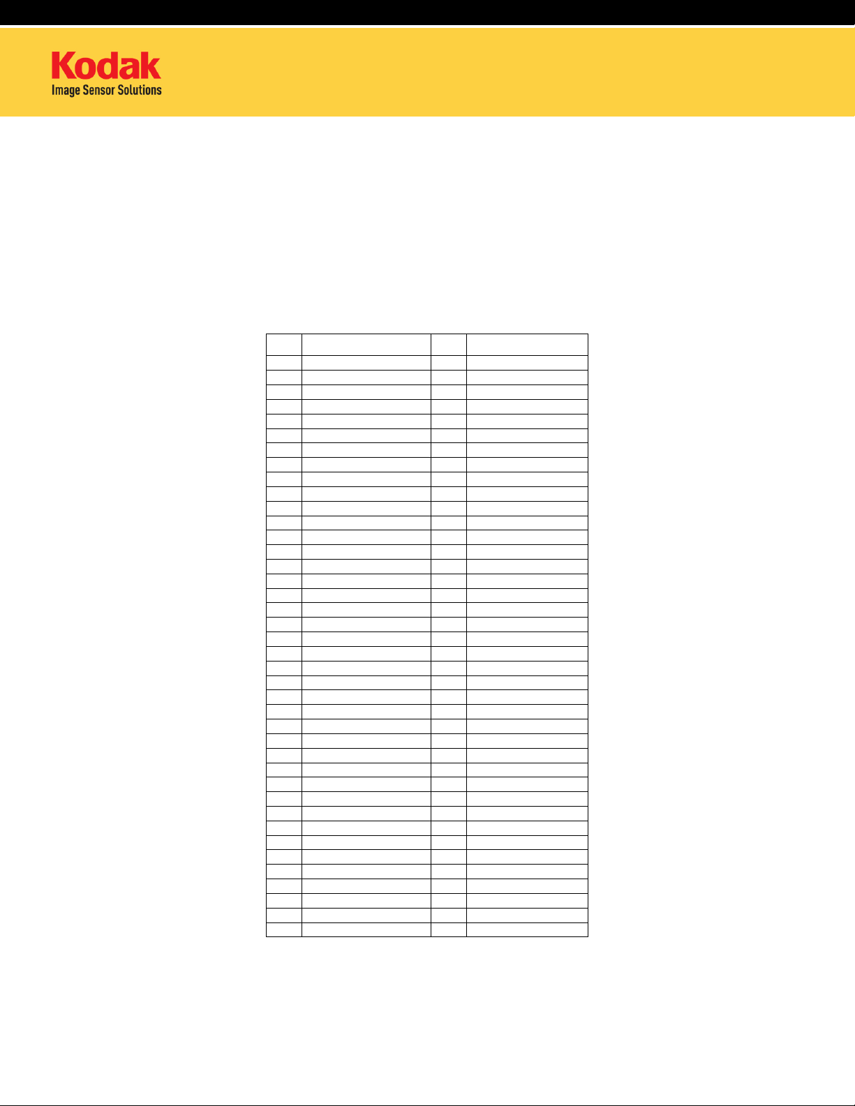
BOARD INTERFACE CONNECTOR J1
Pin Signal Pin Signal
1 N.C. 2 N.C.
3 AGND 4 AGND
5 VES+ 6 VES7 AGND 8 AGND
9 FDG+ 10 FDG11 AGND 12 AGND
13 V3RD+ 14 V3RD15 AGND 16 AGND
17 V2B+ 18 V2B19 AGND 20 AGND
21 V2+ 22 V223 AGND 24 AGND
25 V1+ 26 V127 AGND 28 AGND
29 R+ 30 R31 AGND 32 AGND
33 H2B+ 34 H2B35 AGND 36 AGND
37 H2A+ 38 H2A39 AGND 40 AGND
41 H1B+ 42 H1B43 AGND 44 AGND
45 H1A+ 46 H1A47 N.C. 48 N.C.
49 AGND 50 AGND
51 N.C. 52 N.C.
53 VMINUS_MTR 54 VMINUS_MTR
55 N.C. 56 N.C.
57 AGND 58 AGND
59 AMP_ENABLE+ 60 AMP_ENABLE61 -5V_MTR 62 -5V_MTR
63 N.C. 64 N.C.
65 AGND 66 AGND
67 N.C. 68 N.C.
69 +5V_MTR 70 +5V_MTR
71 N.C. 72 N.C.
73 AGND 74 AGND
75 N.C. 76 N.C.
77 VPLUS_MTR 78 VPLUS_MTR
79 N.C. 80 N.C.
Table 5: J1 Interface Connector Pin Assignments
©Eastman Kodak Company, 2005 www.kodak.com/go/imagers Revision 4.0 (MTD/PS-0521) p8
Page 9
WARNINGS AND ADVISORIES
The Imager Board described in this document is designed for use as part of a two-board set, in conjunction with a Timing
Generator Board. Kodak offers an Imager Board / Timing Generator Board package that has been designed and
configured to operate with the KAI-4011 and KAI-4021 CCD image sensors.
Purchasers of a Kodak Evaluation Board Kit may, at their discretion, make changes to the Timing Generator Board
firmware. Eastman Kodak can only support firmware developed and supplied by Eastman Kodak. Changes to the
firmware are at the risk of the customer.
When programming the Timing Board, the Imager Board must be disconnected from the Timing Board, by removing the
Board Interface Cable before power is applied. If the Imager Board is connected to the Timing Board during the
reprogramming of the Altera PLD, damage to the Imager Board will occur.
GLOSSARY OF ABBREVIATIONS
AGND Analog Ground.
CCD Charge-Coupled Device; also referred as to the image sensor , imager, or device.
FDG Fast Dump Gate; signal drains charge from the Horizontal registers to allow line sampling.
HCLK Horizontal Clock
LVDS Low Voltage Differential Signaling, per the TIA/EIA-644 and IEEE 1596.3 standards.
R+ or R- Reset Clock
SMB Subminiature video connector, 75Ω characteristic impedance.
VCLK Vertical Clock.
V3RD Vertical Clock 3rd-level voltage; initiates frame readout by transferring charge to vertical registers.
VES Electronic Shutter control signal.
REVISION HISTORY
Revision Number Description of Changes
1 Initial Formal Version
2.0 Added Warnings and Advisories Section
3.0 Document now applies to KAI-4011 and KAI-4021 Imagers.
4.0 Added text note on drawings to define ground pins on CCD imager (Product Drawing)
Added Glossary of Abbreviations
Added Revision History
Added information regarding optional One-Shot.
Added metric units to drawing.
©Eastman Kodak Company, 2005 www.kodak.com/go/imagers Revision 4.0 (MTD/PS-0521) p9
Page 10

APPENDICES
KAI-4011/KAI-4021 IMAGER BOARD SCHEMATICS
©Eastman Kodak Company, 2005 www.kodak.com/go/imagers Revision 4.0 (MTD/PS-0521) p10
Page 11

Page 12

Page 13

Page 14

Page 15

Page 16

Page 17

Page 18

Page 19

Page 20

Page 21

Page 22

Page 23

Page 24

Page 25

Page 26

Page 27

Page 28

©Eastman Kodak Company, 2005. Kodak and Pixelux are trademarks.
 Loading...