

Page 1

IMAGE SENSOR SOLUTIONS
KODAK KAI-2001/KAI-2020/KAI-2093
IMAGER EVALUATION BOARD
CCD IMAGE SENSORS
USERS MANUAL
Revision 4.0
April 18, 2005
MTD/PS-0715 Revision 4.0
www.kodak.com/go/imagers 585-722-4385 Fax: 585-477-4947 Email: imagers@kodak.com
Page 1 of 31
Page 2

IMAGE SENSOR SOLUTIONS
TABLE OF CONTENTS
KAI-2001/KAI-2020/KAI-2093 IMAGER EVALUATION BOARD DESCRIPTION ......... 3
IMAGER BOARD INPUT REQUIREMENTS .................................................................. 3
KAI-2001/KAI-2020/KAI-2093 IMAGER BOARD ARCHITECTURE OVERVIEW.......... 5
POWER FILTERING AND REGULATION............................................................................................................ 5
LVDS RECEIVERS / TTL BUFFERS ...............................................................................................................5
CCD PIXEL-RATE CLOCK DRIVERS (H1, H2 & RESET CLOCKS) .................................................................... 5
RESET CLOCK ONE-SHOT............................................................................................................................. 5
CCD VCLK DRIVERS................................................................................................................................... 5
CCD FDG DRIVER..................................................................................................................................... 5
VSUB/VES CIRCUIT.................................................................................................................................. 5
VDD BIAS VOLTAGE ....................................................................................................................................5
ESD BIAS VOLTAGE.....................................................................................................................................6
CCD IMAGE SENSOR.................................................................................................................................... 6
EMITTER-FOLLOWER ....................................................................................................................................6
LINE DRIVERS............................................................................................................................................... 6
KAI-2001/KAI-2020/KAI-2093 OPERATIONAL SETTINGS .......................................... 7
DC BIAS VOLTAGES..................................................................................................................................... 7
CLOCK VOLTAGES ........................................................................................................................................ 7
RESET CLOCK PULSE WIDTH ........................................................................................................................8
BLOCK DIAGRAM AND PERFORMANCE DATA......................................................... 9
CONNECTOR ASSIGNMENTS AND PINOUTS .......................................................... 11
SMB CONNECTORS J1, J2 AND J3............................................................................................................. 11
BOARD INTERFACE CONNECTOR J4 ............................................................................................................ 11
WARNINGS AND ADVISORIES .................................................................................. 12
REFERENCES.............................................................................................................. 12
GLOSSARY OF ABBREVIATIONS.............................................................................. 12
REVISION HISTORY .................................................................................................... 12
APPENDICES............................................................................................................... 13
KAI-2001/KAI-2020/KAI-2093 IMAGER BOARD SCHEMATICS .................................................................... 13
TABLES
Table 1: Power Requirements.................................................................................................................... 3
Table 2: Signal Level Requirements ......................................................................................................... 4
Table 3: DC Bias Voltages.......................................................................................................................... 7
Table 4: Clock Voltages.............................................................................................................................. 7
Table 5: Reset Clock Pulse Width ............................................................................................................. 8
Table 6: J4 Interface Connector Pin Assignments ................................................................................ 11
FIGURES
Figure 1. KAI-2001/KAI-2020/KAI-2093 Imager Board Block Diagram................................................... 9
Figure 2. Measured Performance -- Dynamic Range and Noise Floor ................................................ 10
MTD/PS-0715 Revision 4.0
www.kodak.com/go/imagers 585-722-4385 Fax: 585-477-4947 Email: imagers@kodak.com
Page 2 of 31
Page 3
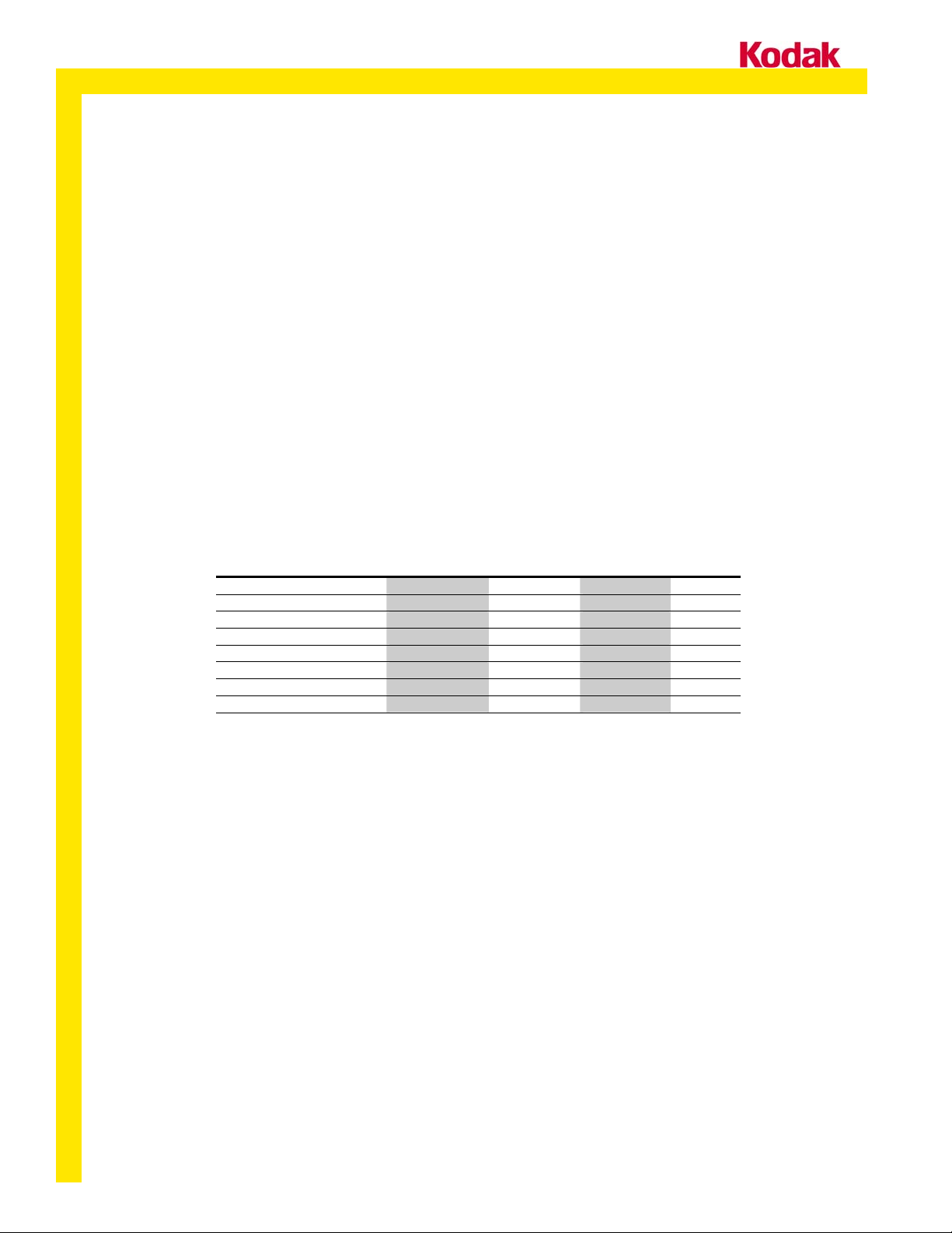
IMAGE SENSOR SOLUTIONS
KAI-2001/KAI-2020/KAI-2093 IMAGER EVALUATION BOARD DESCRIPTION
The KAI-2001/KAI-2020/KAI-2093 Imager
Evaluation Board, referred to in this document as
the Imager Board, is designed to be used as part
of a two-board set, used in conjunction with a
Timing Generator Board. Kodak offers an Imager
Board / Timing Generator Board package that has
been designed and configured to operate with the
KAI-2001, KAI-2020, and KAI-2093 CCD image
sensors.
The Timing Generator Board generates the timing
signals necessary to operate the CCD, and
provides the power required by the Imager Board.
The timing signals, in LVDS format, and the
power, are provided to the Imager Board via the
interface connector (J4). In addition, the Timing
Generator Board performs the processing and
digitization of the analog video output of the
Imager Board.
IMAGER BOARD INPUT REQUIREMENTS
Power Supplies Minimum Typical Maximum Units
+5V_MTR Supply 4.9 5 5.1 V
800 mA
-5V_MTR Supply -5.1 -5 -4.9 V
200 mA
VPLUS Supply 18 20 21 V
250 mA
VMINUS Supply -21 -20 -18 V
250 mA
The Imager Board has been designed to operate
the KAI-2001, KAI-2020, and KAI-2093 CCDs with
the specified performance at nominal operating
conditions. (See the appropriate performance
specifications for details).
For testing and characterization purposes, the
Imager board provides the ability to adjust many of
the CCD bias voltages and CCD clock level
voltages by adjusting potentiometers on the board.
The Imager Board provides the means to modify
other device operating parameters (e.g., CCD
reset clock pulse width) by populating components
differently on the board.
Some circuitry on the Imager Board (e.g., remote
DAC control of bias and clock level voltages) is
intended for Kodak test purposes only, and may
not be populated.
Table 1: Power Requirements
MTD/PS-0715 Revision 4.0
www.kodak.com/go/imagers 585-722-4385 Fax: 585-477-4947 Email: imagers@kodak.com
Page 3 of 31
Page 4
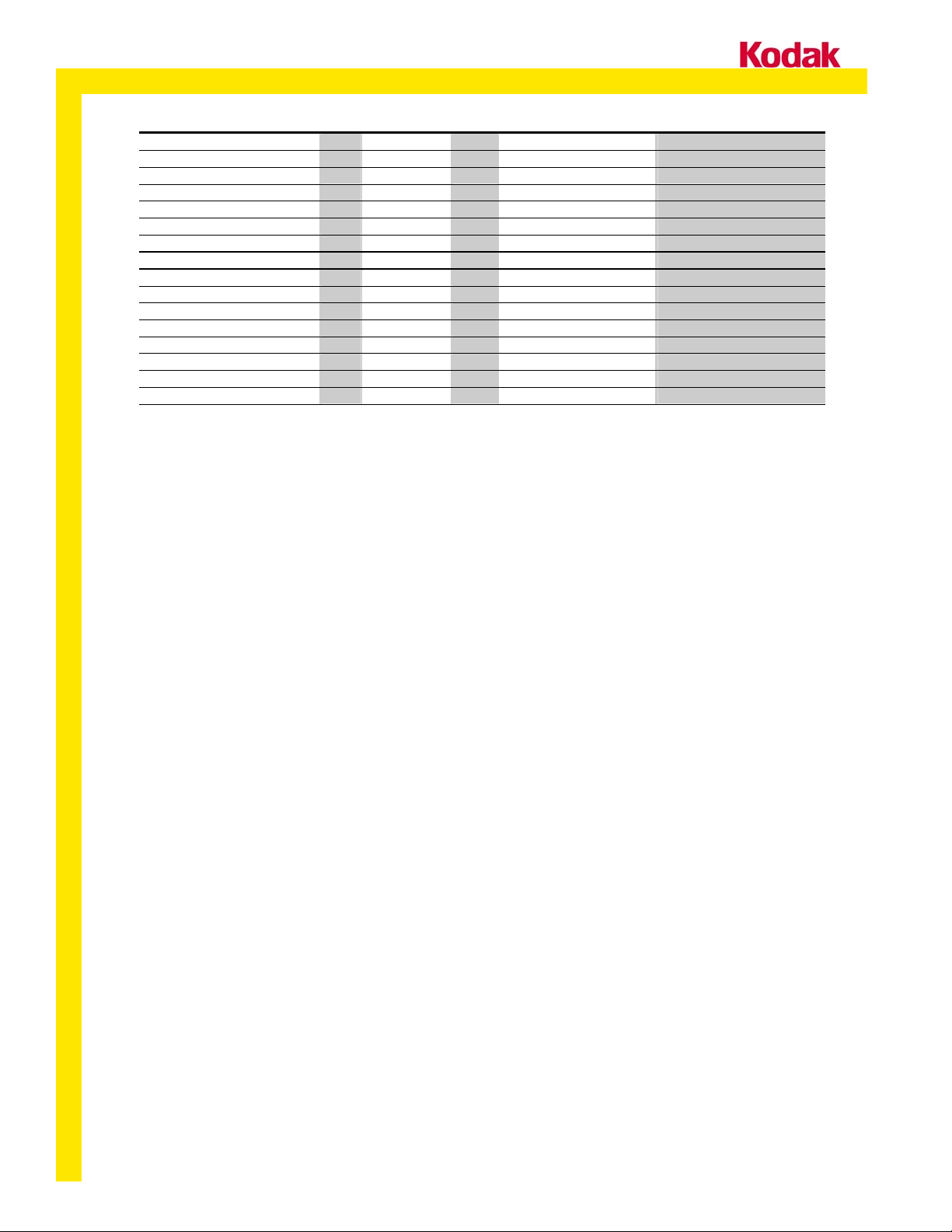
IMAGE SENSOR SOLUTIONS
Input Signals (LVDS) Vmin Vthreshold Vmax Units Signal Comments
IMAGER_IN0
IMAGER_IN1 0 +/- 0.1 2.4 V H1A H1A clock
IMAGER_IN2 0 +/- 0.1 2.4 V H1B H1B clock
IMAGER_IN3 0 +/- 0.1 2.4 V H2A H2A clock
IMAGER_IN4 0 +/- 0.1 2.4 V H2B H2B clock
IMAGER_IN5 0 +/- 0.1 2.4 V RESET Reset clock
IMAGER_IN6 0 +/- 0.1 2.4 V V1 V1 clock
IMAGER_IN7 0 +/- 0.1 2.4 V V2 V2 clock
IMAGER_IN8 0 +/- 0.1 2.4 V (not used)
IMAGER_IN9 0 +/- 0.1 2.4 V V3RD V2 Clock 3rd-level
IMAGER_IN10 0 +/- 0.1 2.4 V FDG Fast Dump clock
IMAGER_IN11 0 +/- 0.1 2.4 V VES Electronic Shutter clock
IMAGER_IN12 0 +/- 0.1 2.4 V VIDEO_SWITCH Vout MUX (J1) control
IMAGER_IN13 0 +/- 0.1 2.4 V (not used)
IMAGER_IN14 0 +/- 0.1 2.4 V (not used)
IMAGER_IN15 0 +/- 0.1 2.4 V (not used)
0 +/- 0.1 2.4 V AMP_ENABLE Output Amplifier Enable
Table 2: Signal Level Requirements
MTD/PS-0715 Revision 4.0
www.kodak.com/go/imagers 585-722-4385 Fax: 585-477-4947 Email: imagers@kodak.com
Page 4 of 31
Page 5

IMAGE SENSOR SOLUTIONS
KAI-2001/KAI-2020/KAI-2093 IMAGER BOARD ARCHITECTURE OVERVIEW
The following sections describe the functional blocks of the Imager board (refer to Figure 1).
Power Filtering And Regulation
Power is supplied to the Imager Board via the J4
interface connector. The power supplies are decoupled and filtered with ferrite beads and
capacitors to suppress noise. Voltage regulators
are used to create the +15 and –15V supplies from
the VPLUS and VMINUS supplies.
LVDS Receivers / TTL Buffers
LVDS timing signals are input to the Imager Board
via the J4 interface connector. These signals are
shifted to TTL levels before being sent to the CCD
clock drivers.
CCD Pixel-Rate Clock Drivers (H1, H2 &
Reset Clocks)
The pixel rate CCD clock drivers utilize two fast
switching transistors that are designed to translate
TTL-level input clock signals to the voltage levels
required by the CCD. The high level and low
levels of the CCD clocks are set by
potentiometers, and are buffered by operational
amplifiers configured as voltage followers.
Reset Clock One-Shot
The pulse width of the RESET_CCD clock may be
set by U13, a programmable One-Shot. The OneShot can be configured to provide a RESET_CCD
clock signal with a pulse width from 5ns to 15ns. If
pulse width control functionality is provided by the
Timing Board, the One-Shot may be removed and
bypassed by installing R147.
CCD VCLK Drivers
The vertical clock (VCLK) drivers consist of
MOSFET driver IC’s. These drivers are designed
to translate the TTL-level clock signals to the
voltage levels required by the CCD. The high,
middle, and low voltage levels of the vertical
clocks are set by potentiometers buffered by
operational amplifiers. The VHIGH and VLOW opamps have a gain of 1.25, to allow the magnitude
of the voltages to be adjusted to 12.5V when using
DAC control.
The current sources for these voltage levels are
high current (up to 600 mA) transistors. The
V2_CCD high level clock voltage is switched from
V_MID to V_HIGH once per frame to transfer the
charge from the photodiodes to the vertical CCDs.
MTD/PS-0715 Revision 4.0
www.kodak.com/go/imagers 585-722-4385 Fax: 585-477-4947 Email: imagers@kodak.com
Page 5 of 31
The V1 clock driver is a 2-level driver circuit,
switching between VMID amd VLOW voltage
levels.
CCD FDG DRIVER
The Fast Dump clock drivers consist of a transistor
that will switch the voltage on the FD pin of the
CCD from FDG_LOW to FDG_HIGH during Fast
Dump Gate operations. When not in operation, or
when the Fast Dump Gate feature is not being
utilized, the FDG pin of the CCD is held at
FDG_LOW. The FDG_HIGH and FDG_LOW
voltage levels of the FDG driver are set by
potentiometers, buffered by operational amplifiers
configured as voltage followers.
The KAI-2093 image sensor does not have the
Fast Dump Gate feature. To support this device,
the Imager Board must be configured so that the
CCD pin 11 is 0.0V. To accomplish this, R91 is
removed, and R79 is installed.
VSUB/VES CIRCUIT
The quiescent CCD substrate voltage (VSUB) is
set by a potentiometer and resistor divider
network. The VSUB voltage is buffered by an
operational amplifier configured with a gain of
1.40, to allow the voltage to be adjusted to nearly
14.0V. A blocking diode prevents the VSUB bias
circuitry from being damaged by the higher-voltage
electronic shutter pulse.
For electronic shutter operation, the VES signal
drives a transistor amplifier circuit that AC-couples
the voltage difference between the VPLUS and
VMINUS supplies onto the Substrate voltage. This
creates the necessary potential to clear all charge
from the photodiodes, thereby acting as an
electronic shutter to control exposure.
VDD Bias Voltage
The VDDL and VDDR video output amplifier
supplies in the CCD are coupled directly to the
+15V regulated supply on the Imager Board. The
Imager Board contains optional circuitry that
allows this voltage to be adjusted through the
Alternate VDD bias circuit.
The Imager Board contains optional Amplifier
Enable circuitry to control a switch that switches
the VDD voltage from +15V to ALT_VDD.
Page 6

IMAGE SENSOR SOLUTIONS
ESD Bias Voltage
The RESET and HCLK gates on the KAI-2001,
KAI-2020, and KAI-2093 CCDs are protected from
ESD damage by internal circuitry. The ESD bias
voltage is set by a potentiometer, buffered by an
operational amplifier configured as a voltage
follower. The ESD bias voltage must be more
negative than any of the protected gates during
operation and powerup. In order to ensure these
conditions are met, diodes are connected external
to the CCD between the protected gates and
VESD, and between VSUB and VESD.
It is also recommended that during powerup of the
Timing Board and Imager Board, the VMINUS
supply is applied before, or simultaneously with,
the other power supplies. For more information,
refer to the appropriate CCD Image Sensor Device
Performance Specifications (References 1, 2 and
3).
CCD Image Sensor
This evaluation board supports the Kodak KAI2001, KAI-2020, and KAI-2093 Interline CCD
image sensors.
Emitter-Follower
The VOUT_LEFT_CCD and VOUT_RIGHT_CCD
video output signals are buffered using bipolar
junction transistors in the emitter-follower
configuration. These circuits also provide the
necessary 5mA current sink for the CCD output
circuits. The voltage gain of this stage is
approximately 0.96.
Line Drivers
The buffered VOUT_LEFT_CCD and
VOUT_RIGHT_CCD signals are AC-coupled and
driven from the Imager Board by operational
amplifiers in a non-inverting configuration. The
operational amplifiers are configured to have a
gain of 1.25, which yields an overall gain of 0.6
when driving the properly terminated 75Ω video
coaxial cabling from the SMB connector. This is
done to prevent overloading the AFE on the
Timing Board.
The video output of either channel may be
multiplexed to the VOUT_MUX output. The
multiplexer is controlled by the VIDEO_MUX
signal. This circuitry is for Kodak use only, and is
not enabled.
MTD/PS-0715 Revision 4.0
www.kodak.com/go/imagers 585-722-4385 Fax: 585-477-4947 Email: imagers@kodak.com
Page 6 of 31
Page 7
IMAGE SENSOR SOLUTIONS
KAI-2001/KAI-2020/KAI-2093 OPERATIONAL SETTINGS
The Imager board is configured to operate the KAI-2001/KAI-2020/KAI-2093 CCD image sensor under
the following operating conditions:
DC Bias Voltages
The following voltages are fixed, or adjusted with a
potentiometer as noted. The nominal values listed
in Table 3 correspond to the device specification
nominal settings at the time of this document’s
publication, and are subject to change. The Min
KAI-2001/
KAI-2020
Description Symbol Min
Output Gate
Reset Drain RD 7.0 12.0 10.5 14.0 V R25
Output Amplifier Supply VDD 15.0 15.0 V Fixed
Alternate Amplifier Supply ALT_VDD 6.0 - - 11.0 V R28
Ground GND 0.0 0.0 V Fixed
Substrate SUB 7.0 Vab Vab 13.0 V R17 1
ESD Protection ESD -6.0 -7.0 -7.0 -11.0 V R27
Output Amplifier Return VSS 0.5 0.7 0.7 5.0 V R29
OG -5.0 -2.0 -2.5 -0.5 V R26
Nominal
and Max voltages in the table indicate the
approximate adjustable voltage range on the
imager board. These values may exceed the
specified CCD operating conditions. See the
appropriate device specifications for details.
KAI-2093
Nominal
Max Units Potentiometer Notes
Table 3: DC Bias Voltages
NOTES:
1. The recommended VSUB voltage is specified for each CCD image sensor, and is labeled on the device container as V
Clock Voltages
The following clock voltage levels are fixed, or
adjusted with a potentiometer as noted. The
nominal values listed in Table 4 correspond to the
device specification nominal settings at the time of
this document’s publication, and are subject to
Description Symbol Level Min
Horizontal CCD Clock
High -5.0 1.0 1.0 5.0 V R129 2
Vertical CCD Clock Vx_CCD Low -12.0 -9.0 -9.0 -6.5 V R66 3
Vx_CCD Mid -3.0 0.0 -1.5 3.0 V R107 4
V2_CCD High 6.5 8.0 8.0 12.0 V R83
Reset Clock RESET_CCD Low -7.5 -3.5 -3.5 -1.0 V R166
High 0.5 1.5 1.5 5.0 V R158
Fast Dump Clock FD_CCD Low -11.0 -9.0 0.0 -4.0 V R108 5
High 2.5 5.0 0.0 5.0 V R93 5
VDD +15V High 15.0 15.0 V Fixed
Hxx_CCD Low -7.5 -4.0 -4.0 -1.0 V R146 1
Table 4: Clock Voltages
change. The Min and Max voltages in the table
indicate the approximate adjustable voltage range
on the imager board. These values may exceed
the specified CCD operating conditions. See the
appropriate device specification for details.
KAI-2001/
KAI-2020
Nom
KAI-2093
Nom
Max Unit
Potenti-
ometer
Notes
.
AB
MTD/PS-0715 Revision 4.0
www.kodak.com/go/imagers 585-722-4385 Fax: 585-477-4947 Email: imagers@kodak.com
Page 7 of 31
Page 8
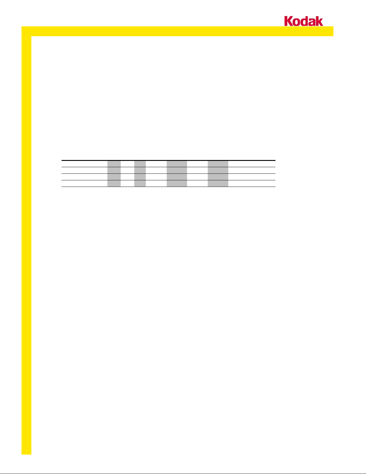
IMAGE SENSOR SOLUTIONS
NOTES:
1. The H1A_CCD, H1B_CCD, H2A_CCD, and H2B_CCD low levels are controlled by the same potentiometer (R146).
2. The H1A_CCD, H1B_CCD, H2A_CCD, and H2B_CCD high levels are controlled by the same potentiometer (R129).
3. V1_CCD and V2_CCD low levels are controlled by the same potentiometer (R66)
4. V1_CCD and V2_CCD mid levels are controlled by the same potentiometer (R107)
5. The KAI-2093 has no Fast Dump Gate; CCD pin 11 is 0.0V. To accomplish this, R91 is removed, and R79 is installed.
Reset Clock Pulse Width
The pulse width of RESET_CCD may be set by
configuring P[2..0], the inputs to the programmable
one-shot U13. P[2..0] can be tied high or low to
achieve the desired pulse width by populating the
resistors R156, R157, R160, and R161
accordingly.
Pulse Width P0 P1 P2 R156 R157 R160 R161 Notes
15ns 0 0 0 IN OUT IN OUT
5ns 1 0 0 OUT IN IN OUT Default Setting
7.5ns 0 1 0 IN OUT OUT IN
10ns 1 1 0 OUT IN OUT IN
This feature is optional, as the RESET pulsewidth
may also be controlled from the Timing Board. In
that case, U13 is removed, and R147 is installed
to bypass this circuitry.
Table 5: Reset Clock Pulse Width
MTD/PS-0715 Revision 4.0
www.kodak.com/go/imagers 585-722-4385 Fax: 585-477-4947 Email: imagers@kodak.com
Page 8 of 31
Page 9
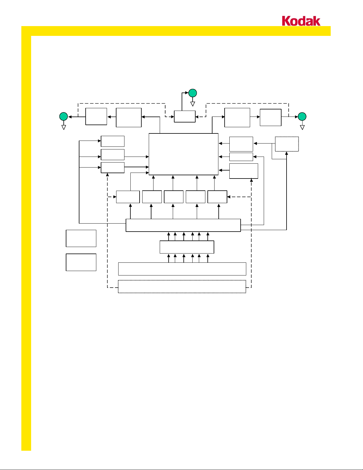
IMAGE SENSOR SOLUTIONS
BLOCK DIAGRAM AND PERFORMANCE DATA
J3
SMB
LINE
DRIVER
EMITTER
FOLLOWER
Video
Switch
SMB
J1
J2
SMB
EMITTER
FOLLOWER
LINE
DRIVER
+15V
REGULATOR
-15V
REGULATOR
V3RD
DRIVER
V2
DRIVER
V1
DRIVER
VSUB/
VES CKT
VOUT
LEFT
CCD
SENSOR
H1A
DRIVER
H2A
DRIVER
LVDS TO TTL BUFFERS
LVDS RECEIVERS
J4 BOARD INTERFACE CONNECTOR
P1 DAC CONNECTOR (optional)
H1B
DRIVER
VOUT
RIGHT
H2B
DRIVER
RCLK
DRIVER
FD CKT
DC BIASES:
ESD, OG, RD,
ALT_VDD, VSS
RCLK
1 SHOT
(optional)
Figure 1. KAI-2001/KAI-2020/KAI-2093 Imager Board Block Diagram
MTD/PS-0715 Revision 4.0
www.kodak.com/go/imagers 585-722-4385 Fax: 585-477-4947 Email: imagers@kodak.com
Page 9 of 31
Page 10

IMAGE SENSOR SOLUTIONS
100
10
Noise (A/D counts)
1
1 10 100 1000 10000 100000
Photon Transfer
Slope = el/A du = 9.19 electrons
Nois e f loor = 2.47 counts (22.7
electrons )
LVSA T = 32027 electrons
VSA T = 35758 electrons
Signal Mean (Electrons)
Figure 2. KAI-2020 Measured Performance -- Dynamic Range and Noise Floor
MTD/PS-0715 Revision 4.0
www.kodak.com/go/imagers 585-722-4385 Fax: 585-477-4947 Email: imagers@kodak.com
Page 10 of 31
Page 11

IMAGE SENSOR SOLUTIONS
CONNECTOR ASSIGNMENTS AND PINOUTS
SMB Connectors J1, J2 and J3
The emitter-follower buffered VOUT_LEFT and
VOUT_RIGHT signals are driven from the Imager
Board via the SMB connectors J3 and J2,
respectively. VOUT_LEFT is the primary output
from the CCD; VOUT_RIGHT is only used when
the CCD is clocked in dual-channel mode.
Coaxial cable with a characteristic impedance of
75 Ω should be used to connect the imager board
Board Interface Connector J4
Pin Signal Pin Signal
1 N.C. 2 N.C.
3 AGND 4 AGND
5 IMAGER_IN11+ 6 IMAGER_IN11-
7 AGND 8 AGND
9 IMAGER_IN10+ 10 IMAGER_IN10-
11 AGND 12 AGND
13 IMAGER_IN9+ 14 IMAGER_IN9-
15 AGND 16 AGND
17 IMAGER_IN8+ 18 IMAGER_IN8-
19 AGND 20 AGND
21 IMAGER_IN7+ 22 IMAGER_IN7-
23 AGND 24 AGND
25 IMAGER_IN6+ 26 IMAGER_IN6-
27 AGND 28 AGND
29 IMAGER_IN5+ 30 IMAGER_IN5-
31 AGND 32 AGND
33 IMAGER_IN4+ 34 IMAGER_IN4-
35 AGND 36 AGND
37 IMAGER_IN3+ 38 IMAGER_IN3-
39 AGND 40 AGND
41 IMAGER_IN2+ 42 IMAGER_IN2-
43 AGND 44 AGND
45 IMAGER_IN1+ 46 IMAGER_IN1-
47 N.C. 48 N.C.
49 AGND 50 AGND
51 N.C. 52 N.C.
53 VMINUS_MTR 54 VMINUS_MTR
55 N.C. 56 N.C.
57 AGND 58 AGND
59 IMAGER_IN0+ 60 IMAGER_IN0-
61 -5V_MTR 62 -5V_MTR
63 IMAGER_IN15+ 64 IMAGER_IN15-
65 AGND 66 AGND
67 IMAGER_IN14+ 68 IMAGER_IN14-
69 +5V_MTR 70 +5V_MTR
71 IMAGER_IN13+ 72 IMAGER_IN13-
73 AGND 74 AGND
75 IMAGER_IN12+ 76 IMAGER_IN12-
77 VPLUS_MTR 78 VPLUS_MTR
79 N.C. 80 N.C.
to the Timing Generator Board to match the series
and terminating resistors used on these boards.
J1 is an auxiliary SMB connector driven from a
relay. The relay switches between the
VOUT_LEFT and VOUT_RIGHT signals, allowing
one video connection to transmit either output.
Table 6: J4 Interface Connector Pin Assignments
MTD/PS-0715 Revision 4.0
www.kodak.com/go/imagers 585-722-4385 Fax: 585-477-4947 Email: imagers@kodak.com
Page 11 of 31
Page 12

IMAGE SENSOR SOLUTIONS
WARNINGS AND ADVISORIES
The Imager Board described in this document is designed to be used as part of a two-board set, in
conjunction with a Timing Generator Board. Kodak offers an Imager Board / Timing Generator Board
package that has been designed and configured to operate with the KAI-2001, KAI-2020, and KAI-2093
CCD image sensors.
Purchasers of a Kodak Evaluation Board Kit may, at their discretion, make changes to the Timing
Generator Board firmware. Eastman Kodak can only support firmware developed by, and supplied by,
Eastman Kodak. Changes to the firmware are at the risk of the customer.
When programming the Timing Board, the Imager Board should be disconnected from the Timing Board,
by removing the Board Interface Cable before power is applied. If the Imager Board is connected to the
Timing Board during the reprogramming of the Altera PLD, damage to the Imager Board may occur.
When applying power to the Evaluation Board Kit, care should be taken that the VMINUS supply is
applied before, or simultaneously with, the other power supplies.
REFERENCES
1. KAI-2001 CCD Image Sensor Device Performance Specification
2. KAI-2020 CCD Image Sensor Device Performance Specification
3. KAI-2093 CCD Image Sensor Device Performance Specification
Kodak reserves the right to change any information contained herein without notice. All information
furnished by Kodak is believed to be accurate.
GLOSSARY OF ABBREVIATIONS
AGND Analog Ground.
CCD Charge-Coupled Device; also referred as to the image sensor , imager, or device.
FDG Fast Dump Gate; signal drains charge from the Horizontal registers to allow line sampling.
HCLK Horizontal Clock
LVDS Low Voltage Differential Signaling, per the TIA/EIA-644 and IEEE 1596.3 standards.
R+ or R- Reset Clock
SMB Subminiature video connector, 75Ω characteristic impedance.
VCLK Vertical Clock.
V3RD Vertical Clock 3
VES Electronic Shutter control signal.
rd
-level voltage; initiates frame readout by transferring charge to vertical registers.
REVISION HISTORY
Revision
Number
1
2 Revision 2 Product Drawing; change to FD_HIGH limits (Table 4)
3 Revision 3 Product Drawing; added KAI-2001 CCD. (3F5121 assembly is still Rev 2)
4.0 Revision 4 Product Drawing; added KAI-2093 CCD. (3F5121 assembly is Rev 4)
Initial Formal Version
Description of Changes
MTD/PS-0715 Revision 4.0
www.kodak.com/go/imagers 585-722-4385 Fax: 585-477-4947 Email: imagers@kodak.com
Page 12 of 31
Page 13

IMAGE SENSOR SOLUTIONS
APPENDICES
KAI-2001/KAI-2020/KAI-2093 Imager Board Schematics
MTD/PS-0715 Revision 4.0
www.kodak.com/go/imagers 585-722-4385 Fax: 585-477-4947 Email: imagers@kodak.com
Page 13 of 31
Page 14

Page 15

Page 16

Page 17

Page 18

Page 19

Page 20

Page 21

Page 22

Page 23

Page 24

Page 25

Page 26

Page 27

Page 28

Page 29

Page 30

 Loading...