

Page 1

Sample Application Programs Guide Book
Agilent 4155C Semiconductor Parameter Analyzer
Agilent 4156C Precision Semiconductor Parameter Analyzer
Agilent Part No. 04156-90070
Printed in Japan January 2001
Edition 1
Page 2

Legal Notice
The information contained in this document is subject to change without notice.
Copyright © 2001 Agilent Technologies
This document contains information which is protected by copyright. All rights are
reserved. Reproduction, adaptation, or translation without prior written permission is
prohibited, except as allowed under the copyright laws.
• Product Warranty
Agilent Technologies warrant Agilent Technologies hardware, accessories and supplies
against defects in materials and workmanship for the period of one year from the
warranty start date specified below. If Agilent Technologies receive notice of such
defects during the warranty period, Agilent Technologies will, at its option, either
repair or replace products which prove to be defective. Replacement products may be
either new or like-new.
Warranty service of this product will be performed at Agilent Technologies. Buyer
shall prepay shipping charges to Agilent Technologies and Agilent Technologies shall
pay shipping charges to return the product to Buyer. However, Buyer shall pay all
shipping charges, duties, and taxes for products returned to Agilent Technologies from
another country.
Agilent Technologies do not warrant that the operation of Agilent Technologies
products will be uninterrupted or error free. If Agilent is unable, within a reasonable
time, to repair or replace any product to a condition as warranted, customer will be
entitled to a refund of the purchase price upon prompt return of the product.
The Agilent Technologies products may contain remanufactured parts equivalent to
new in performance or may have been subject to incidental use.
The warranty period begins on the date of delivery or on the date of installation if
installed by Agilent Technologies. If customer schedules or delays Agilent
Technologies installation more than 30 days after delivery, warranty begins on the 31st
day from delivery.
Warranty does not apply to defects resulting from (a) improper or inadequate
maintenance or calibration, (b) software, interfacing, parts or supplies not supplied by
Agilent Technologies, (c) unauthorized modification or misuse, (d) operation outside of
the published environmental specifications for the product, or (e) improper site
preparation or maintenance.
To the extent allowed by local law, the above warranties are exclusive and no other
warranty or condition, whether written or oral, is expressed or implied and Agilent
Technologies specifically disclaim any implied warranties or conditions of
merchantability, satisfactory quality, and fitness for a particular purpose.
Agilent Technologies will be liable for damage to tangible property per incident up to
the greater of $300,000 or the actual amount paid for the product that is the subject of
the claim, and for damages for bodily injury or death, to the extent that all such
damages are determined by a court of competent jurisdiction to have been directly
caused by a defective Agilent Technologies product.
2 Agilent 4155C/4156C Sample Application Programs Guide Book, Edition 1
Page 3

To the extent allowed by local law, the remedies in this warranty statement are
customer’s sole and exclusive remedies. Expect as indicated above, in no event will
Agilent Technologies or its suppliers be liable for loss of date or for direct, special,
incidental, consequential (including lost profit or date), or other damage, whether based
in contract, tort, or otherwise.
For consumer transactions in Australia and New Zealand: the warranty terms contained
in this statement, except to the extent lawfully permitted, do not exclude, restrict or
modify and are in addition to the mandatory statutory rights applicable to the sale of
this product to you.
• Assistance
Product maintenance agreements and other customer assistance agreements are
available for Agilent Technologies products.
For any assistance, contact your nearest Agilent Technologies Sales Office.
• Certification
Agilent Technologies Inc. certifies that this product met its published specifications at
the time of shipment from the factory. Agilent further certifies that its calibration
measurements are traceable to the National Institute of Standards and Technology
(NIST), to the extent allowed by the Institute’s calibration facility, and to the
calibration facilities of other International Standards Organization members.
Printing History
Edition 1: January 2001
Agilent 4155C/4156C Sample Application Programs Guide Book, Edition 1 3
Page 4

In This Manual
This manual describes some sample application programs and setup files, which will be
helpful for creating your own applications using Agilent 4155C/4156C.
All programs and setup files described in this manual are stored on the Sample Application
Program Disk (DOS formatted, 3.5-inch diskette) that is furnished with your
4155C/4156C. All programs are written in the Instrument BASIC, and ready to run in the
4155C/4156C’s built-in Instrument BASIC environment.
This manual covers the following applications:
• V- RA M P
• J-RAMP
• SWEAT
• GO/NO-GO Test
• HCI Degradation Test
• Charge Pumping
• Flash EEPROM Test
• TDDB
• Electromigration
CAUTION These programs are only examples, so you may need to modify these programs and setup
files for your own application before executing. If these example programs damage your
devices, Agilent Technologies is NOT LIABLE for the damage.
NOTE You should copy all files in the Sample Application Program Disk to a diskette that you
will use as your working diskette, and keep the original diskette as backup.
4 Agilent 4155C/4156C Sample Application Programs Guide Book, Edition 1
Page 5

Contents
1. V-RAMP
Theory of V-Ramp Test Procedure . . . . . . . . . . . . . . . . . . . . . . . . . . . . . . . . . . . . 1-3
V-Ramp Test Overview . . . . . . . . . . . . . . . . . . . . . . . . . . . . . . . . . . . . . . . . . . . 1-3
Initial Test . . . . . . . . . . . . . . . . . . . . . . . . . . . . . . . . . . . . . . . . . . . . . . . . . . . . . 1-4
Post Stress Test . . . . . . . . . . . . . . . . . . . . . . . . . . . . . . . . . . . . . . . . . . . . . . . . . 1-4
Ramp Stress Test . . . . . . . . . . . . . . . . . . . . . . . . . . . . . . . . . . . . . . . . . . . . . . . . 1-5
Failure Categorization and Data Recording . . . . . . . . . . . . . . . . . . . . . . . . . . . 1-7
Basic Operation . . . . . . . . . . . . . . . . . . . . . . . . . . . . . . . . . . . . . . . . . . . . . . . . . . . 1-8
Methodology . . . . . . . . . . . . . . . . . . . . . . . . . . . . . . . . . . . . . . . . . . . . . . . . . . . 1-8
Required Equipment . . . . . . . . . . . . . . . . . . . . . . . . . . . . . . . . . . . . . . . . . . . . 1-16
Files on the Diskette . . . . . . . . . . . . . . . . . . . . . . . . . . . . . . . . . . . . . . . . . . . . 1-16
Executing the VRAMP Program . . . . . . . . . . . . . . . . . . . . . . . . . . . . . . . . . . . 1-17
Flowchart of Sample VRAMP Program . . . . . . . . . . . . . . . . . . . . . . . . . . . . . 1-18
Customization . . . . . . . . . . . . . . . . . . . . . . . . . . . . . . . . . . . . . . . . . . . . . . . . . . . 1-20
Using an External Computer . . . . . . . . . . . . . . . . . . . . . . . . . . . . . . . . . . . . . . 1-20
Specifying Setup File to Load . . . . . . . . . . . . . . . . . . . . . . . . . . . . . . . . . . . . . 1-21
File for Saving Measurement Results . . . . . . . . . . . . . . . . . . . . . . . . . . . . . . . 1-21
Setting up Input Parameters . . . . . . . . . . . . . . . . . . . . . . . . . . . . . . . . . . . . . . . 1-22
Searching for 10 ¥ Iexpect . . . . . . . . . . . . . . . . . . . . . . . . . . . . . . . . . . . . . . . . 1-23
Measurement Setups . . . . . . . . . . . . . . . . . . . . . . . . . . . . . . . . . . . . . . . . . . . . . . 1-24
Setups for Initial and Post Stress Tests . . . . . . . . . . . . . . . . . . . . . . . . . . . . . . 1-24
Setups for Ramped Stress Test . . . . . . . . . . . . . . . . . . . . . . . . . . . . . . . . . . . . 1-24
2. J-RAMP
Theory of J-Ramp Test Procedure . . . . . . . . . . . . . . . . . . . . . . . . . . . . . . . . . . . . . 2-3
J-Ramp Test Overview . . . . . . . . . . . . . . . . . . . . . . . . . . . . . . . . . . . . . . . . . . . 2-3
Initial Test . . . . . . . . . . . . . . . . . . . . . . . . . . . . . . . . . . . . . . . . . . . . . . . . . . . . . 2-4
J-Ramp Stress Test . . . . . . . . . . . . . . . . . . . . . . . . . . . . . . . . . . . . . . . . . . . . . . . 2-5
Post Stress Test . . . . . . . . . . . . . . . . . . . . . . . . . . . . . . . . . . . . . . . . . . . . . . . . . 2-7
Failure Categorization and Data Recording . . . . . . . . . . . . . . . . . . . . . . . . . . . 2-8
Basic Operation . . . . . . . . . . . . . . . . . . . . . . . . . . . . . . . . . . . . . . . . . . . . . . . . . . . 2-9
Methodology . . . . . . . . . . . . . . . . . . . . . . . . . . . . . . . . . . . . . . . . . . . . . . . . . . . 2-9
Required Equipment . . . . . . . . . . . . . . . . . . . . . . . . . . . . . . . . . . . . . . . . . . . . 2-20
Program Files Required . . . . . . . . . . . . . . . . . . . . . . . . . . . . . . . . . . . . . . . . . . 2-20
Executing the JRAMP Program . . . . . . . . . . . . . . . . . . . . . . . . . . . . . . . . . . . 2-20
Flowchart of Sample JRAMP Program . . . . . . . . . . . . . . . . . . . . . . . . . . . . . . 2-22
Customization . . . . . . . . . . . . . . . . . . . . . . . . . . . . . . . . . . . . . . . . . . . . . . . . . . . 2-24
Using an External Computer . . . . . . . . . . . . . . . . . . . . . . . . . . . . . . . . . . . . . . 2-24
Specifying Setup File to Load . . . . . . . . . . . . . . . . . . . . . . . . . . . . . . . . . . . . . 2-25
Agilent 4155C/4156C Sample Application Programs Guide Book, Edition 1 Contents - 1
Page 6

Contents
File for Saving Measurement Results . . . . . . . . . . . . . . . . . . . . . . . . . . . . . . . 2-25
Setting up Input Parameters . . . . . . . . . . . . . . . . . . . . . . . . . . . . . . . . . . . . . . 2-26
When SMU Lacks Power to Break Oxide . . . . . . . . . . . . . . . . . . . . . . . . . . . 2-27
Measurement Setups . . . . . . . . . . . . . . . . . . . . . . . . . . . . . . . . . . . . . . . . . . . . . . 2-28
Setups for Initial and Post Stress Tests . . . . . . . . . . . . . . . . . . . . . . . . . . . . . . 2-28
Setups for Ramped Stress Test . . . . . . . . . . . . . . . . . . . . . . . . . . . . . . . . . . . . 2-28
Proof of Equations . . . . . . . . . . . . . . . . . . . . . . . . . . . . . . . . . . . . . . . . . . . . . . . 2-36
Step Increase Factor (F). . . . . . . . . . . . . . . . . . . . . . . . . . . . . . . . . . . . . . . . . . 2-36
Step Time (Step_time) . . . . . . . . . . . . . . . . . . . . . . . . . . . . . . . . . . . . . . . . . . . 2-36
Current Stop Value (Istop) . . . . . . . . . . . . . . . . . . . . . . . . . . . . . . . . . . . . . . . 2-36
3. SWEAT
SWEAT . . . . . . . . . . . . . . . . . . . . . . . . . . . . . . . . . . . . . . . . . . . . . . . . . . . . . . . . . 3-3
Overview . . . . . . . . . . . . . . . . . . . . . . . . . . . . . . . . . . . . . . . . . . . . . . . . . . . . . . 3-3
Input Parameters . . . . . . . . . . . . . . . . . . . . . . . . . . . . . . . . . . . . . . . . . . . . . . . . 3-4
Initial Resistance (Rinit) Measurement . . . . . . . . . . . . . . . . . . . . . . . . . . . . . . . 3-5
CTTF . . . . . . . . . . . . . . . . . . . . . . . . . . . . . . . . . . . . . . . . . . . . . . . . . . . . . . . . . 3-5
Rfail . . . . . . . . . . . . . . . . . . . . . . . . . . . . . . . . . . . . . . . . . . . . . . . . . . . . . . . . . . 3-5
Exit Condition . . . . . . . . . . . . . . . . . . . . . . . . . . . . . . . . . . . . . . . . . . . . . . . . . . 3-5
Output Parameters . . . . . . . . . . . . . . . . . . . . . . . . . . . . . . . . . . . . . . . . . . . . . . . 3-6
Basic Operation . . . . . . . . . . . . . . . . . . . . . . . . . . . . . . . . . . . . . . . . . . . . . . . . . . 3-7
Methodology . . . . . . . . . . . . . . . . . . . . . . . . . . . . . . . . . . . . . . . . . . . . . . . . . . . 3-7
Required Equipment . . . . . . . . . . . . . . . . . . . . . . . . . . . . . . . . . . . . . . . . . . . . 3-10
Files on the Diskette . . . . . . . . . . . . . . . . . . . . . . . . . . . . . . . . . . . . . . . . . . . . 3-10
Execution . . . . . . . . . . . . . . . . . . . . . . . . . . . . . . . . . . . . . . . . . . . . . . . . . . . . 3-11
Sample SWEAT Program Overview . . . . . . . . . . . . . . . . . . . . . . . . . . . . . . . . 3-12
Customization . . . . . . . . . . . . . . . . . . . . . . . . . . . . . . . . . . . . . . . . . . . . . . . . . . . 3-13
Using External Computer or Built-in Controller . . . . . . . . . . . . . . . . . . . . . . 3-13
Specifying Setup File to Load . . . . . . . . . . . . . . . . . . . . . . . . . . . . . . . . . . . . . 3-13
File for Saving Measurement Results . . . . . . . . . . . . . . . . . . . . . . . . . . . . . . . 3-14
Setting up Input Parameters . . . . . . . . . . . . . . . . . . . . . . . . . . . . . . . . . . . . . . 3-15
Setting up Input Parameters Related to CTTF Calculation . . . . . . . . . . . . . . . 3-15
How to Reduce the Settling Time of CTTF . . . . . . . . . . . . . . . . . . . . . . . . . . 3-16
Defining JSTART . . . . . . . . . . . . . . . . . . . . . . . . . . . . . . . . . . . . . . . . . . . . . . 3-18
Current Adjustment Routine . . . . . . . . . . . . . . . . . . . . . . . . . . . . . . . . . . . . . . 3-18
Setup files . . . . . . . . . . . . . . . . . . . . . . . . . . . . . . . . . . . . . . . . . . . . . . . . . . . . . . 3-19
Setup File for Initial Resistance Measurement . . . . . . . . . . . . . . . . . . . . . . . . 3-19
Setup File for Stress/Resistance Measurement . . . . . . . . . . . . . . . . . . . . . . . . 3-19
Contents - 2 Agilent 4155C/4156C Sample Application Programs Guide Book, Edition 1
Page 7

Contents
4. Go/NO-GO
GONOGO Sample Program . . . . . . . . . . . . . . . . . . . . . . . . . . . . . . . . . . . . . . . . . 4-3
Basic Operation . . . . . . . . . . . . . . . . . . . . . . . . . . . . . . . . . . . . . . . . . . . . . . . . . . . 4-5
Required Equipment . . . . . . . . . . . . . . . . . . . . . . . . . . . . . . . . . . . . . . . . . . . . . 4-5
Files on the Diskette . . . . . . . . . . . . . . . . . . . . . . . . . . . . . . . . . . . . . . . . . . . . . 4-5
Sample Devices . . . . . . . . . . . . . . . . . . . . . . . . . . . . . . . . . . . . . . . . . . . . . . . . . 4-6
Connection . . . . . . . . . . . . . . . . . . . . . . . . . . . . . . . . . . . . . . . . . . . . . . . . . . . . . 4-6
Execution . . . . . . . . . . . . . . . . . . . . . . . . . . . . . . . . . . . . . . . . . . . . . . . . . . . . . . 4-7
Viewing All Curves while Measurement is in Progress . . . . . . . . . . . . . . . . . 4-10
Viewing Only Results while Measurement is in Progress . . . . . . . . . . . . . . . . 4-11
Viewing a Particular Measurement Curve . . . . . . . . . . . . . . . . . . . . . . . . . . . . 4-12
Changing Limits . . . . . . . . . . . . . . . . . . . . . . . . . . . . . . . . . . . . . . . . . . . . . . . 4-13
Displaying Statistical Data . . . . . . . . . . . . . . . . . . . . . . . . . . . . . . . . . . . . . . . 4-13
Exporting Data to Spreadsheet . . . . . . . . . . . . . . . . . . . . . . . . . . . . . . . . . . . . 4-14
Customization . . . . . . . . . . . . . . . . . . . . . . . . . . . . . . . . . . . . . . . . . . . . . . . . . . . 4-15
Overview . . . . . . . . . . . . . . . . . . . . . . . . . . . . . . . . . . . . . . . . . . . . . . . . . . . . . 4-15
Hints to Use with Handler . . . . . . . . . . . . . . . . . . . . . . . . . . . . . . . . . . . . . . . . 4-21
5. HCI Degradation Test
Hot-Carrier-Induced (HCI) Degradation Test . . . . . . . . . . . . . . . . . . . . . . . . . . . . 5-3
Overview . . . . . . . . . . . . . . . . . . . . . . . . . . . . . . . . . . . . . . . . . . . . . . . . . . . . . . 5-3
Determining Stress Bias Conditions . . . . . . . . . . . . . . . . . . . . . . . . . . . . . . . . . 5-4
Selecting Test Devices . . . . . . . . . . . . . . . . . . . . . . . . . . . . . . . . . . . . . . . . . . . . 5-4
Initial Characterization . . . . . . . . . . . . . . . . . . . . . . . . . . . . . . . . . . . . . . . . . . . 5-4
Parameter Definitions . . . . . . . . . . . . . . . . . . . . . . . . . . . . . . . . . . . . . . . . . . . . 5-5
Stress Cycle . . . . . . . . . . . . . . . . . . . . . . . . . . . . . . . . . . . . . . . . . . . . . . . . . . . . 5-6
Interim Characterization . . . . . . . . . . . . . . . . . . . . . . . . . . . . . . . . . . . . . . . . . . 5-6
Stress Termination . . . . . . . . . . . . . . . . . . . . . . . . . . . . . . . . . . . . . . . . . . . . . . . 5-6
Precautions . . . . . . . . . . . . . . . . . . . . . . . . . . . . . . . . . . . . . . . . . . . . . . . . . . . . 5-6
Technical Requirements . . . . . . . . . . . . . . . . . . . . . . . . . . . . . . . . . . . . . . . . . . 5-7
HCI Degradation Test Data Analysis . . . . . . . . . . . . . . . . . . . . . . . . . . . . . . . . . . 5-8
Basic Operation . . . . . . . . . . . . . . . . . . . . . . . . . . . . . . . . . . . . . . . . . . . . . . . . . . 5-11
Methodology . . . . . . . . . . . . . . . . . . . . . . . . . . . . . . . . . . . . . . . . . . . . . . . . . . 5-11
Input Parameters . . . . . . . . . . . . . . . . . . . . . . . . . . . . . . . . . . . . . . . . . . . . . . . 5-11
HCI Degradation Test . . . . . . . . . . . . . . . . . . . . . . . . . . . . . . . . . . . . . . . . . . . 5-15
HCI Degradation Data Analysis . . . . . . . . . . . . . . . . . . . . . . . . . . . . . . . . . . . 5-16
Required Equipment . . . . . . . . . . . . . . . . . . . . . . . . . . . . . . . . . . . . . . . . . . . . 5-17
Files on the Diskette . . . . . . . . . . . . . . . . . . . . . . . . . . . . . . . . . . . . . . . . . . . . 5-18
Execution . . . . . . . . . . . . . . . . . . . . . . . . . . . . . . . . . . . . . . . . . . . . . . . . . . . . . 5-19
Sample HCI Degradation Test Program (DCDAHC) Overview . . . . . . . . . . . 5-27
Agilent 4155C/4156C Sample Application Programs Guide Book, Edition 1 Contents - 3
Page 8

Contents
Sample HCI Degradation Test Data Analysis Program (ANALYSIS) Overview 5-30
Customization . . . . . . . . . . . . . . . . . . . . . . . . . . . . . . . . . . . . . . . . . . . . . . . . . . . 5-32
Using External Computer or Built-in Controller . . . . . . . . . . . . . . . . . . . . . . 5-32
Modifying and Specifying Setup File to Load . . . . . . . . . . . . . . . . . . . . . . . . 5-33
Changing File for Saving Measurement Results . . . . . . . . . . . . . . . . . . . . . . . 5-34
Changing Input Parameters for HCI Degradation Test . . . . . . . . . . . . . . . . . . 5-35
To Change Pin Assignment . . . . . . . . . . . . . . . . . . . . . . . . . . . . . . . . . . . . . . . 5-37
To Change Number of Test Devices . . . . . . . . . . . . . . . . . . . . . . . . . . . . . . . . 5-37
Changing the Cumulative Stress Times . . . . . . . . . . . . . . . . . . . . . . . . . . . . . 5-38
Skipping Determination of Gate Stress Bias Condition . . . . . . . . . . . . . . . . . 5-38
Reducing the Interval between Stress and Interim Measurement . . . . . . . . . . 5-39
Selecting Parameter Shift Graphs to Draw . . . . . . . . . . . . . . . . . . . . . . . . . . . 5-39
If You Don't Use Switching Matrix . . . . . . . . . . . . . . . . . . . . . . . . . . . . . . . . 5-40
Using Another Switching Matrix . . . . . . . . . . . . . . . . . . . . . . . . . . . . . . . . . . 5-40
Performing HCI Degradation Test with AC Stress . . . . . . . . . . . . . . . . . . . . . 5-41
Performing Reverse Mode Test . . . . . . . . . . . . . . . . . . . . . . . . . . . . . . . . . . . . 5-42
Changing Input Parameters for Test Data Analysis . . . . . . . . . . . . . . . . . . . . 5-43
Not to Pause Program after each Tdc Extraction . . . . . . . . . . . . . . . . . . . . . . 5-43
Changing File Name to save Calculated Average Tdc . . . . . . . . . . . . . . . . . . 5-43
Setup Files . . . . . . . . . . . . . . . . . . . . . . . . . . . . . . . . . . . . . . . . . . . . . . . . . . . . . 5-44
Setup File for Id-Vd Measurement to Determine Drain Stress Voltage . . . . . 5-44
Setup File for Ib-Vg Measurement to Determine Gate Stress Voltage . . . . . . 5-46
Setup File for Gate Leakage Current Measurement . . . . . . . . . . . . . . . . . . . . 5-49
Setup File for Initial/Interim Characterization . . . . . . . . . . . . . . . . . . . . . . . . 5-52
Setup File for DC Stress . . . . . . . . . . . . . . . . . . . . . . . . . . . . . . . . . . . . . . . . . 5-55
Setup File for AC Stress . . . . . . . . . . . . . . . . . . . . . . . . . . . . . . . . . . . . . . . . . 5-56
6. Charge Pumping
Charge Pumping Methods . . . . . . . . . . . . . . . . . . . . . . . . . . . . . . . . . . . . . . . . . . 6-3
Square Pulse Method . . . . . . . . . . . . . . . . . . . . . . . . . . . . . . . . . . . . . . . . . . . . 6-3
Triangular Pulse Method . . . . . . . . . . . . . . . . . . . . . . . . . . . . . . . . . . . . . . . . . . 6-3
Trapezoidal Pulse Method . . . . . . . . . . . . . . . . . . . . . . . . . . . . . . . . . . . . . . . . . 6-3
Equipment Required . . . . . . . . . . . . . . . . . . . . . . . . . . . . . . . . . . . . . . . . . . . . . . . 6-4
Square Pulse Method . . . . . . . . . . . . . . . . . . . . . . . . . . . . . . . . . . . . . . . . . . . . . . 6-5
To Extract Interface-state Density . . . . . . . . . . . . . . . . . . . . . . . . . . . . . . . . . . . 6-5
Program Files Required . . . . . . . . . . . . . . . . . . . . . . . . . . . . . . . . . . . . . . . . . . 6-7
Sample Setup File . . . . . . . . . . . . . . . . . . . . . . . . . . . . . . . . . . . . . . . . . . . . . . . 6-7
To Execute the Sample Program . . . . . . . . . . . . . . . . . . . . . . . . . . . . . . . . . . . 6-10
Square Pulse Method without Program . . . . . . . . . . . . . . . . . . . . . . . . . . . . . . . 6-13
Requirement . . . . . . . . . . . . . . . . . . . . . . . . . . . . . . . . . . . . . . . . . . . . . . . . . . 6-13
Contents - 4 Agilent 4155C/4156C Sample Application Programs Guide Book, Edition 1
Page 9

Contents
Sample Setup File . . . . . . . . . . . . . . . . . . . . . . . . . . . . . . . . . . . . . . . . . . . . . . 6-13
To Execute the Measurement . . . . . . . . . . . . . . . . . . . . . . . . . . . . . . . . . . . . . 6-16
Triangular Pulse Method . . . . . . . . . . . . . . . . . . . . . . . . . . . . . . . . . . . . . . . . . . . 6-17
To Extract Interface-state Density . . . . . . . . . . . . . . . . . . . . . . . . . . . . . . . . . . 6-18
To Extract Capture Cross Section . . . . . . . . . . . . . . . . . . . . . . . . . . . . . . . . . . 6-19
Program Files Required . . . . . . . . . . . . . . . . . . . . . . . . . . . . . . . . . . . . . . . . . . 6-20
Sample Setup File . . . . . . . . . . . . . . . . . . . . . . . . . . . . . . . . . . . . . . . . . . . . . . 6-20
To Execute the Sample Program . . . . . . . . . . . . . . . . . . . . . . . . . . . . . . . . . . . 6-24
Trapezoidal Pulse Method . . . . . . . . . . . . . . . . . . . . . . . . . . . . . . . . . . . . . . . . . . 6-27
To Extract Interface-state Density . . . . . . . . . . . . . . . . . . . . . . . . . . . . . . . . . . 6-28
Program Files Required . . . . . . . . . . . . . . . . . . . . . . . . . . . . . . . . . . . . . . . . . . 6-30
Sample Setup File . . . . . . . . . . . . . . . . . . . . . . . . . . . . . . . . . . . . . . . . . . . . . . 6-30
To Execute the Sample Program . . . . . . . . . . . . . . . . . . . . . . . . . . . . . . . . . . . 6-33
Program Modification Examples . . . . . . . . . . . . . . . . . . . . . . . . . . . . . . . . . . . . 6-36
To Change the Initial Value of Input Parameters . . . . . . . . . . . . . . . . . . . . . . . 6-36
To Change the Measurement Unit . . . . . . . . . . . . . . . . . . . . . . . . . . . . . . . . . . 6-42
To Change the Destination of the File Operation . . . . . . . . . . . . . . . . . . . . . . 6-45
7. Flash EEPROM Test
Program Overview . . . . . . . . . . . . . . . . . . . . . . . . . . . . . . . . . . . . . . . . . . . . . . . . 7-3
Device Connection for NOR type flash EEPROM . . . . . . . . . . . . . . . . . . . . . . 7-3
Device Connection for NAND type flash EEPROM . . . . . . . . . . . . . . . . . . . . . 7-4
Main Program. . . . . . . . . . . . . . . . . . . . . . . . . . . . . . . . . . . . . . . . . . . . . . . . . . . 7-5
Stress_loop . . . . . . . . . . . . . . . . . . . . . . . . . . . . . . . . . . . . . . . . . . . . . . . . . . . . 7-7
Vth_meas . . . . . . . . . . . . . . . . . . . . . . . . . . . . . . . . . . . . . . . . . . . . . . . . . . . . . . 7-8
Program Customization . . . . . . . . . . . . . . . . . . . . . . . . . . . . . . . . . . . . . . . . . . . . . 7-9
Subprogram “Test_setting” . . . . . . . . . . . . . . . . . . . . . . . . . . . . . . . . . . . . . . . . 7-9
Measurement setup file for Vth measurement (for NOR type) . . . . . . . . . . . . 7-10
Stress setup file for write pulse of NOR type. . . . . . . . . . . . . . . . . . . . . . . . . . 7-11
Stress setup file for erase pulse of NOR type. . . . . . . . . . . . . . . . . . . . . . . . . . 7-11
Stress setup file for write pulse of NAND type . . . . . . . . . . . . . . . . . . . . . . . . 7-12
Stress setup file for erase pulse of NAND type . . . . . . . . . . . . . . . . . . . . . . . . 7-12
Program Listing . . . . . . . . . . . . . . . . . . . . . . . . . . . . . . . . . . . . . . . . . . . . . . . . . . 7-13
8. Time Dependent Dielectric Breakdown (TDDB)
Application Overview . . . . . . . . . . . . . . . . . . . . . . . . . . . . . . . . . . . . . . . . . . . . . . 8-3
Customization . . . . . . . . . . . . . . . . . . . . . . . . . . . . . . . . . . . . . . . . . . . . . . . . . . . . 8-4
Agilent 4155C/4156C Sample Application Programs Guide Book, Edition 1 Contents - 5
Page 10

Contents
9. Electromigration
Application Overview . . . . . . . . . . . . . . . . . . . . . . . . . . . . . . . . . . . . . . . . . . . . . . 9-3
Customization . . . . . . . . . . . . . . . . . . . . . . . . . . . . . . . . . . . . . . . . . . . . . . . . . . . . 9-4
Contents - 6 Agilent 4155C/4156C Sample Application Programs Guide Book, Edition 1
Page 11

1V-RAMP
Page 12

V-RAMP
Voltage-Ramped (V-Ramp) test is one of the Wafer Level Reliability (WLR) tests, which is
used to evaluate device reliability on a wafer. This test can provide quick evaluation data
for estimating the overall reliability of thin oxides, and this data can be used to improve the
thin oxide manufacturing process.
With the thickness of oxide shrinking along with device geometries, creating a reliable thin
oxide has become an important issue. The integrity of the thin oxide in a MOS device is a
dominant factor in determining the overall reliability of a micro-circuit. The V-Ramp test
can promptly give useful feedback to the manufacturing process about oxide reliability.
This operation manual covers a sample V-Ramp program running on Agilent 4155/4156,
and how to use and customize the program. The program is written in the Instrument
BASIC (IBASIC), and is ready to run on the built-in IBASIC controller of the 4155/4156.
“Theory of V-Ramp Test Procedure” describes basic theory, procedure, and terminology of
the V-Ramp test.
“Basic Operation” describes the V-Ramp sample program. Included are V-Ramp
methodology using the 4155/4156, how to execute the sample program, and program
overview.
“Customization” describes how to customize the sample program. This is very helpful
because you probably need to modify the sample program to suit your test device.
“Measurement Setups” shows the 4155/4156 page settings that are stored in the setup files.
1-2 Agilent 4155C/4156C Sample Application Programs Guide Book, Edition 1
Page 13

V-RAMP
Theory of V-Ramp Test Procedure
Theory of V-Ramp Test Procedure
This section describes the Voltage-Ramped (V-Ramp) Test procedure. Included are basic
theory, procedure, and terminology of V-Ramp test. The V-Ramp test procedure is based on
JEDEC standard No.35.
V-Ramp Test Overview
V-Ramp test measures the breakdown voltage (Vbd) and breakdown charge (Qbd) of thin
oxide capacitors, which you designed as test structures on the wafer. These results are used
to evaluate the oxide integrity. The higher the Vbd and Qbd measured by this test, the better
the integrity of the oxide on wafer.
You extract these two parameters from a large amount of test structures and extracted
parameters are used for standard process control to quickly evaluate oxide integrity.
In the V-Ramp test, an increasing voltage is forced to the oxide capacitor until the oxide
layer is broken. Breakdown voltage (Vbd) is defined as the voltage at which breakdown
occurs. And breakdown charge (Qbd) is the total charge forced through the oxide until the
breakdown occurs.
Figure 1-1 shows a simplified flowchart of V-Ramp test.
Figure 1-1 Simplified Flow Diagram of V-Ramp Test
Agilent 4155C/4156C Sample Application Programs Guide Book, Edition 1 1-3
Page 14

V-RAMP
Theory of V-Ramp Test Procedure
The V-Ramp test consists of three tests: initial test, ramp stress test, and post stress test.
In the initial test, normal operating voltage is applied to the oxide capacitor, then leakage
current through the capacitor is measured to check for initial failure.
In the ramp stress test, linear ramped voltage is applied to the capacitor, and the current is
measured.
The post stress test is for confirming that failure occurred during the ramp stress test. The
normal operating voltage is applied to the oxide capacitor again, and leakage current is
measured under the same conditions as the initial test.
After the tests, the test results must be analyzed and saved (data recording).
Before performing the V-Ramp test, test conditions must satisfy the following:
• Gate bias polarity is in accumulated direction. That is, negative (minus) voltage is
applied to gate conductor for P-type bulk, and positive (plus) voltage is applied for
N-type bulk.
• Diffusions and wells (if any) must be connected to substrate.
• Temperature is in 25 ± 5 °C range.
Initial Test
Initial test is to confirm that the oxide capacitor is initially good. If leakage current of that
capacitor exceeds 1 mA, it is categorized as initial failure.
For example, when you test a TTL-level oxide capacitor, constant voltage of -5 V is
applied to that capacitor, and leakage current is measured. If the leakage current is more
than 1 mA, that capacitor is an initial failure.
Post Stress Test
The post stress test checks the oxide status after the ramp stress test. If the oxide is broken,
proper ramp stress was applied to the oxide capacitor. If not, maybe the ramp stress was not
applied correctly.
To check the oxide status, the normal operating voltage is applied to the oxide capacitor
(same as initial test), then leakage current is measured. The leakage current (I
indicates the following:
• If I
• If I
> 1 mA:
leak
The oxide was broken by the applied ramped voltage.
< 1 mA:
leak
The oxide was not broken by the applied ramped voltage.
If the applied ramped voltage reached the maximum electric field, the testing was
probably faulty: for example, the ramped voltage was not applied to the oxide due to an
open circuit.
leak
) value
For example, if you test a TTL level oxide capacitor, constant voltage of -5 V is applied to
that capacitor, then leakage current is measured. If the leakage current is more than 1 mA,
the capacitor was properly broken.
1-4 Agilent 4155C/4156C Sample Application Programs Guide Book, Edition 1
Page 15

V-RAMP
Theory of V-Ramp Test Procedure
Ramp Stress Test
A linear ramped voltage or a linear stepped voltage, which is approximately ramped
voltage, is applied to the oxide capacitor. While the ramped voltage is forced, the current
through the oxide is measured.
The ramped voltage is stopped when one of the following conditions occurs:
• Current through the oxide exceeds ten times the expected current. The expected current
is calculated from the applied voltage and structure of oxide capacitor. For example, the
expected current density J for a 200 angstrom oxide capacitor is calculated from the
equation for Fowler-Nordheim current as follows:
2 B
æö
JAE
Where, A and B are constants in terms of effective mass and barrier height.E is electric
field.
exp×=
---
–
èø
E
• Current through the oxide exceeds the current compliance determined by the current
density compliance limit of 20 A/cm
2
.
• Electric field generated by the applied voltage exceeds 15 MV/cm. This typically
indicates faulty testing.
Figure 1-2 shows the concept of Vbd and Qbd. In the graph, left vertical axis shows current
through the oxide, right vertical axis shows voltage applied to the oxide capacitor, and
horizontal axis shows time.
When the current through the oxide reaches 10 times the expected current, the ramped
voltage is stopped, and the applied voltage at this point is the breakdown voltage (Vbd).
Breakdown charge (Qbd) is calculated by integrating the current through the oxide:
Tbd
=
Qbd Imeas t() td
ò
Tstart
Figure 1-2 Concept of Breakdown Voltage and Charge
Agilent 4155C/4156C Sample Application Programs Guide Book, Edition 1 1-5
Page 16

V-RAMP
Theory of V-Ramp Test Procedure
Figure 1-3 shows the two ways to apply the voltage: linear ramped voltage or linear
stepped voltage.
Note that the applied ramped voltage must satisfy the following conditions:
• Ramp rate is in range from 0.1 MV/cm×s to 1.0 MV/cm×s.
• Current measurement interval is 0.1 s or less.
• Ramped voltage starts at normal operating voltage or lower.
• Ramped voltage stops if electric field reaches 15 MV/cm.
If you use the linear stepped voltage, the following conditions must be satisfied also:
• Step value of ramped voltage is 0.1 MV/cm or less.
• Current measurement must be performed at least once for every step.
Figure 1-3 Linear Ramped and Linear Stepped Voltage
1-6 Agilent 4155C/4156C Sample Application Programs Guide Book, Edition 1
Page 17

Failure Categorization and Data Recording
According to the measurement results, the oxide status is categorized as follows and
recorded:
Initial Failure: Failed the initial test. Indicates initially defective oxide
Catastrophic Failure: Failed ramped and post stress tests. Indicates that oxide
Masked Catastrophic Failure: Did not fail ramped stress test, but failed post stress test.
Non-catastrophic Failure: Failed ramped stress test, but not post stress test.
Other Did not fail ramped stress test or post stress test.
The failure category is recorded for each test device. If the catastrophic failure is observed,
breakdown voltage (Vbd) and breakdown charge density (q
recorded.
Table 1-1 shows the oxide failure categories.
Table 1-1 Oxide Failure Categories
V-RAMP
Theory of V-Ramp Test Procedure
capacitor. Other tests should not be performed.
capacitor was properly broken by the ramped stress test.
= Qbd/Area) are also
bd
Failure Category Initial Test
Ramp Stress
Test
Post Stress Test
Initial Fail n.a. n.a.
Catastrophic
a
Pass Fail Fail
Masked Catastrophic Pass Pass Fail
Non-catastrophic Pass Fail Pass
Other Pass Pass Pass
a. Vbd and qbd are also recorded.
Agilent 4155C/4156C Sample Application Programs Guide Book, Edition 1 1-7
Page 18

V-RAMP
Basic Operation
Basic Operation
This section covers the following for using an 4155/4156 to perform V-Ramp Test:
required equipment, required files, methodology, how to execute the sample program, and
sample program overview.
Methodology
The entire V-Ramp Test procedure can be performed by executing the VRAMP sample
program on the built-in IBASIC controller of the 4155/4156.
As explained in “Theory of V-Ramp Test Procedure”, the V-Ramp test consists of three
measurement parts and an analysis part. Each measurement part executes three steps as
follows:
1. Loads the measurement setup file into the 4155/4156 execution environment.
2. Changes some of the measurement or analysis parameters on the setup pages.
3. Executes the measurement.
The VRAMP program executes the above three steps for each test: initial test, ramp stress
test, and post stress test. Using the measurement setups (step 1 above) loaded from a file
reduces the length and complexity of the program. For details, see Programmer's Guide.
Measurement setups, which are loaded into the 4155/4156 execution environment, were
previously developed and saved to measurement setup files on the diskette. You can easily
modify the measurement setup information in fill-in-the-blank manner in the 4155/4156
execution environment. The VRAMP sample program is also saved to the diskette. You
can easily modify the sample program by using the editor in the built-in IBASIC
environment.
The VRAMP sample program assumes that the built-in IBASIC controller of the
4155/4156 is used, but you can also use another controller, such as HP BASIC running on
an external computer. To do so, you must modify the sample program for your
environment. See “Customization” on how to modify the program to run on an external
controller.
Initial Test
The initial test makes sure the oxide capacitor is initially good by applying the normal
operating voltage (Vuse), then measuring the leakage current (I
I
exceeds 1 mA, the oxide capacitor is categorized as "initial failure".
leak
The sample program assumes that SMU1 and SMU4 are connected to the oxide capacitor
as shown in Figure 1-4.
) through the oxide. If
leak
1-8 Agilent 4155C/4156C Sample Application Programs Guide Book, Edition 1
Page 19

V-RAMP
Basic Operation
For the initial test, the sample program does as follows:
1. Sets up the 4155/4156 according to the VRSPOT.MES setup file, which the sample
program previously loaded from the diskette into internal memory MEM1.
2. Sets up SMU1 to constant voltage Vuse for PMOS device, or -Vuse for NMOS
device. Vuse value is specified previously in the sample program, and reset on the
MEASURE: SAMPLING SETUP page by OUTPUT statement (line 2550 of the
sample program).
3. Forces voltage from SMU1, then measures current after the HOLD TIME, which was
setup by VRSPOT.MES setup file described next.
4. Checks if current through the oxide Ig exceeds 1 mA. If so, the sample program aborts
further testing.
The following are main points about the setup by the VRSPOT.MES setup file:
• On CHANNELS: CHANNEL DEFINITION page (see Figure 1-13)
• MEASUREMENT MODE is set to SAMPLING.
• SMU1 and SMU4 are set to be constant voltage sources.
• Ig is defined as name of current measured by SMU1.
• On MEASURE: SAMPLING SETUP page (see Figure 1-5)
• NO. OF SAMPLES is set to 1 to execute the measurement once.
• HOLD TIME is set to 2.00 s to allow the output voltage to stabilize.
• SMU4 is set to force a constant 0 V.
• STOP CONDITION is enabled, NAME is set to Ig, THRESHOLD is set to 1 mA,
and EVENT is set to Val > Th.
So, the measurement will stop if the current through the oxide (Ig) exceeds 1 mA.
If so, the sample program will abort further testing.
Figure 1-4 Simplified Measurement Circuit and Output Voltage of Initial Test
Agilent 4155C/4156C Sample Application Programs Guide Book, Edition 1 1-9
Page 20

V-RAMP
Basic Operation
Figure 1-5 MEASURE: SAMPLING SETUP Page for Initial Test
Ramp Stress Test
After the initial test, the sample program executes the ramp stress test. Linear stepped
voltage is applied to the oxide.
The measurement setup for the ramp stress test is stored in the VRSWEP.MES setup file on
the diskette. At the beginning of the sample program, this setup is loaded into internal
memory (MEM2). Then, at the beginning of the ramp stress test, the sample program loads
this setup into the 4155/4156.
To force proper stepped voltage, the sample program and VRSWEP.MES set the following:
• SMU channel definition (see Figure 1-6):
SMU4 is set to force a constant 0 V, and SMU1 is set to voltage sweep mode.
• Constant step interval time (see Figure 1-8):
Step interval time of output sweep voltage must be constant.
• Measurement stop mode:
If the current through the oxide reaches the specified compliance, the voltage sweep
and measurement stops.
• Auto-analysis and user functions:
After the measurement, the 4155/4156 executes analysis automatically to search for
Vbd, and to calculate Qbd.
1-10 Agilent 4155C/4156C Sample Application Programs Guide Book, Edition 1
Page 21

SMU Channel Definition.
The sample program assumes the connection between the SMUs and the oxide capacitor as
shown in Figure 1-6. SMU4 is set to force a constant 0 V, and SMU1 is set to voltage
sweep mode by the VRSWEP.MES setup as shown in Figure 1-7.
Figure 1-6 Simplified Measurement Circuit of Ramp Stress Test
V-RAMP
Basic Operation
Figure 1-7 CHANNELS: CHANNEL DEFINITION Page for Ramp Stress Test
Agilent 4155C/4156C Sample Application Programs Guide Book, Edition 1 1-11
Page 22

V-RAMP
Basic Operation
Constant step interval time.
To keep a constant step interval time for the voltage sweep and measurement, triggering
and measurement ranging techniques are used. VRSWEP.MES sets the measurement
ranging mode to FIXED, so the time between measurements does not vary due to range
changing.
VRSWEP.MES enables the TRIG OUT function, and the sample program calculates and
sets values so that the step interval time becomes constant as shown in Figure 1-8. The step
interval time (Step_time) is the delay time (Step_delay_t) plus step delay time
(Step_keep_t). Strictly speaking, the sample program calculates these as follows:
Step_time=Vstep/(Ramp_rate*Tox)-1.2ms+0.1ms
Step_delay_t=Step_time/2
Step_keep_t=Step_time-Step_delay_t
Where,
• 1.2 ms is overhead time associated with the delay time for voltage sweep measurement,
when the WAIT TIME field is set to 0 (zero). So, do not set another value in this field.
• 0.1 ms is overhead time associated with the TRIG OUT function.
• Ramp rate (Ramp_rate), oxide thickness (Tox), and step voltage (Vstep) are
specified in lines 1800 to 1840 of the sample program.
The start voltage (Vstart), stop voltage (Vstop), and step voltage (Vstep) are
specified in sample program in lines 1830 to 1850. For NMOS devices, the ramp stress test
subprogram actually sets the opposite polarity for these values by using the Tp variable.
Measurement stop mode.
NOTE The JEDEC standard says that the ramp stress test should abort when the current through
the oxide reaches 10 times the expected current (Iexpect). But this sample program
aborts when the current reaches current compliance (Igcomp). The Iexpect and
Igcomp values are specified in lines 1860 and 1870 of the sample program, and must
meet the following condition: Igcomp ³ Iexpect ´ 10.
VRSWEP.MES file sets the sweep stop condition to SWEEP STOP AT COMPLIANCE as
shown in the Figure 1-10.
Figure 1-8 Output Sweep Voltage for Ramp Stress Test
1-12 Agilent 4155C/4156C Sample Application Programs Guide Book, Edition 1
Page 23

V-RAMP
Basic Operation
Figure 1-9 MEASURE: MEASURE SETUP and OUTPUT SEQUENCE Pages for Ramp Stress
Test
Figure 1-10 MEASURE: SWEEP SETUP Page for Ramp Stress Test
Agilent 4155C/4156C Sample Application Programs Guide Book, Edition 1 1-13
Page 24

V-RAMP
Basic Operation
Auto-analysis and user functions.
The sample program does the following:
1. Sets up the maximum and minimum values for graph axes: X, Y1, and Y2. Lines 2940
to 2980.
2. Performs the measurement. Line 3020.
3. Moves marker to maximum Ig, and saves value to Igmax. Lines 3100 to 3170.
4. Moves marker to position where Ig = Iexpect*10. Line 3200.
5. If compliance was reached or if Igmax ³ Iexpect*10, the sample program reads
the value of Vbd and Qbd at present marker position. Lines 3250 to 3320. Where Vdb
and Qbd are specified as described below.
The VRSWEP.MES setup file defines user functions on the CHANNELS: USER
FUNCTION DEFINITION page (see Figure 1-20) as follows:
Table 1-2 User Functions for Ramp Stress Test
Name Units Definition
Time (sec)
@INDEX * 1
a
Vbd (V) @MY2
Qbd (Q) INTEG(Ig,Time)
a. This is a temporary value. Value of Time is redefined by line 2810 of the
sample program.
The above user function calculates Qbd as follows:
Tbd
Qbd Imeas t() td
==
ò
Tstart
N
1
-- - Imeas
å
2
i 2=
Imeas
+()TiT
i
i 1–
–()´
i 1–
Where, N is step number when the breakdown occurs.
1-14 Agilent 4155C/4156C Sample Application Programs Guide Book, Edition 1
Page 25

Post Stress Test
Post stress test checks the oxide status after the ramp stress test.
The methodology of the post stress test is the same as for initial test. The normal operating
voltage (Vuse) is applied to the oxide, then the leakage current (I
For the measurement circuit, connections, and measurement setups, see “Initial Test”.
Failure Categorization
Table 1-3 shows the oxide failure categories that are determined by the sample program.
The failure category is displayed for each device, and Vbd, Qbd, and qbd are also
displayed.
The measured data and measurement settings are saved in a file.
Table 1-3 Oxide Failure Categories
Basic Operation
) is measured.
leak
V-RAMP
Category Initial Test Ramp Stress Test
Initial I
Catastrophic I
> 1 mA n.a. n.a.
meas
£ 1 mAI
meas
meas
³ I
expect
I compliance reached.
Masked Catastrophic I
£ 1 mAI
meas
meas
< I
expect
I compliance not reached.
Non-catastrophic I
£ 1 mAI
meas
meas
³ I
expect
I compliance reached.
Other I
£ 1 mAI
meas
meas
< I
expect
I compliance not reached.
´ 10, or
´ 10, and
´ 10, or
´ 10, and
Post Stress
Test
I
> 1 mA
meas
I
> 1 mA
meas
I
£ 1 mA
meas
I
£ 1 mA
meas
Agilent 4155C/4156C Sample Application Programs Guide Book, Edition 1 1-15
Page 26

V-RAMP
Basic Operation
Required Equipment
The following equipment is required to use the V-Ramp sample program:
• Agilent 4155 or Agilent 4156 Semiconductor Parameter Analyzer
• Two triaxial cables
• Probe station
• This operation manual
• Diskette that contains sample program file and two setup files
Files on the Diskette
The following files are stored in the sample diskette:
VRAMP V-Ramp sample program. This is an IBASIC program file saved in
ASCII format.
VRSPOT.MES Measurement setup file for initial and post stress test.
VRSWEP.MES Measurement setup file for ramp stress test.
1-16 Agilent 4155C/4156C Sample Application Programs Guide Book, Edition 1
Page 27

V-RAMP
V
Basic Operation
Executing the VRAMP Program
Before executing the program, you may need to customize the program to suit your test
device. See “Customization”.
To execute the sample program, use the following procedure:
1. Connect your 4155/4156 to your test device. See Figure 1-4.
2. Turn on your 4155/4156.
3. Insert the diskette containing the VRAMP program into the built-in 3.5 inch flexible
disk drive.
4. Press
Display key in the IBASIC area of the front panel until All IBASIC screen is
displayed.
5. Load the VRAMP program. Type: GET "VRAMP" and press
6. Press
RUN key in the IBASIC area of the front panel to start the program.
Measurement results similar to Figure 1-11 will be displayed on the GRAPHICS page of
the 4155/4156.
Figure 1-11 An Example of Measurement Results
GRAPH/ LI ST: GRAPHI CS SHORT 9 4OCT 23 1 0: 5 3A M
ol t ag e Ramp Sweep Meas ur emen t
MARKER( 28. 1250 000 sec - 50. 0048mA - 27. 450 V )
( A) Qbd - 13. 059987500mQ ( V)
-1.00 -40. 0
Ig Vg
decade ------
/div /div
Vbd - 27. 4 50000000 V
Enter key.
Vs ub
0. 00 V
100. mA
VSU1
0. 00 V
o
VSU2
0. 00 V
*
- 1. 00p -5. 00
0. 00 Ti me ( sec) 5. 00 / di v 43. *
STATUS:008000(8------- -)
AXI S
Y1
MA R K E R/
CURSOR
L I NE SCAL I NG DI SPL AY
SETUP
SWEEP
SETUP
TI MI NG
SET UP
B
CONST
SETUP
Note that this example is obtained when the maximum electric field is set to 50 MV/cm.
Agilent 4155C/4156C Sample Application Programs Guide Book, Edition 1 1-17
Page 28

V-RAMP
Basic Operation
Flowchart of Sample VRAMP Program
Figure 1-12 shows flowchart of sample VRAMP program and corresponding subprogram
names.
Figure 1-12 Flowchart of Sample VRAMP Program
1-18 Agilent 4155C/4156C Sample Application Programs Guide Book, Edition 1
Page 29

V-RAMP
Basic Operation
The following provides a brief description for each subprogram.
Test_setting Specifies and checks the parameter values. These are values that the
program will set directly instead of some of the setup file values.
Get_file Loads measurement setup files from the diskette into internal memory:
spot measurement setup into MEM1, and sweep measurement setup
into MEM2. Having the measurement setups in internal memory
reduces the measurement time.
Init_fin_test Executes the spot measurement for initial test or for post stress test.
First parameter specifies the test: Init is for initial test, and Fin is
for post stress test. The measurement results are returned to the second
parameter.
Judge Categorizes failure according to measurement results of initial, ramped
stress, and post stress tests. If the failure is initial failure, this
subprogram aborts the program.
Sweep_test Executes sweep measurement for ramped stress test, then returns the
result flag, Vbd, and Qbd to the three parameters. The measurement
result data is temporarily stored in internal memory (MEM3).
Save_data Saves measurement result data (that is in MEM3) to a file on the
diskette.
Agilent 4155C/4156C Sample Application Programs Guide Book, Edition 1 1-19
Page 30

V-RAMP
Customization
Customization
This section describes how to customize the sample program to suit your test device.
Using an External Computer
This sample program (VRAMP) is assumed to run on the Instrument BASIC that is built
into the 4155/4156. The 4155/4156 is used as both the measurement instrument and the
controller running IBASIC, so VRAMP sets device selector 800. On the following three
lines, the 4155/4156 is assigned and interrupt from it is enabled as follows:
1470 ASSIGN @Hp4155 TO 800
:
1540 ON INTR 8 CALL Err_check
1550 ENABLE INTR 8;2
If you use an external controller (that can run HP BASIC environment) to control the
4155/4156, you need to modify a few lines of the sample program. For example, if you use
HP BASIC/WS on an HP 9000 Series 300 computer, you only need to modify lines the
above three lines as follows:
In this case, the 4155/4156 has GPIB address 17 and is not used as the system controller,
and is connected to the built-in GPIB of the HP 9000 series 300 controller with an GPIB
cable. Use the following procedure to set the GPIB address and system mode:
1. Turn on your 4155/4156.
2. Press
3. Select MISCELLANEOUS softkey.
4. Move the field pointer to the "415x is " field, then select the NOT CONTROLLER
5. Move the field pointer to the "415x" field in the GPIB ADDRESS area, then enter: 17.
1-20 Agilent 4155C/4156C Sample Application Programs Guide Book, Edition 1
System key.
softkey.
Page 31
V-RAMP
Customization
System Mode
GPIB Address
SYSTEM: MI SCELL ANEOUS 99 DEC10 0 4 : 42 PM
* 41 56 B i s * POWER L I NE FREQUENCY
NOT S YS T EM CONT ROL L E R 50 H z
* GPI B ADDRESS *414156B NETWORK SETUP
4156B 17 HOST NAME
HARD COPY 1 I P A DDRES S 0 . 0. 0. 0
* REMOT E CONT ROL GROU P I D 1 0 0
COMMAND SET 4155/ 56
*CLOCK TEXT OUT -h
YMDHM GRAPHOUT-h-l
19 99 1 2 10 16 4 2 SERVER T YPE BSD
*SYSTEM SETUP *NETWORK DRI VE SETUP
BEEP ON LABEL
SCREEN SAVE 30 mi n I P ADDRESS 0. 0. 0. 0
LP TI MEOUT 300 s ec DI RECTORY /
NOT SYSTEM CONTROLLER
Sel ect Syst em Cont r ol Mode wi t h sof t key or r ot ar y knob.
FI LER MI SCEL-
LANEOUS
CONFI G CAL I B/
USER I D 200
* NETWORK PRI NTER SETUP
PRI NTER
IP ADDRESS 0.0.0.0
DI AG
PRI NT
SETUP
COLOR
SETUP
Specifying Setup File to Load
CON-
TROLLER
NOT
CON-
TROLLER
Two setup files are used to set up the 4155/4156 for the V-Ramp test: one is used for initial
and post stress tests, and the other is for ramp stress test.
Filenames of these setups are defined on the following lines:
1730 Init_file$="VRSPOT.MES" !Spot Measurement Setup File Name
1740 Sweep_file$="VRSWEP.MES" !Sweep Measurement Setup File Name
If you want to use other setup files, store the setup files on the diskette, then modify the
filenames on the lines above.
File for Saving Measurement Results
The following lines specify the filename for the measurement results file. The filename
starts with "D", then HHMMS, then ends with ".DAT". Where HH is hour, MM is minute,
and S is second (tens digit only).
1750 Save_file$=TIME$(TIMEDATE) !File Name for saving measurement
results
1760 Save_file$="D"&Save_file$[1,2]&Save_file$[4,5]&Save_file$[7,7]&".D
AT"
The following line commands the 4155/4156 to create the specified file on the diskette,
then stores the result data in the file.
3860 OUTPUT @Hp4155;":MMEM:STOR:TRAC DEF,'"&Save_file$&"','DISK'"
For example, "D09344.DAT" file that contains measurement data is created on the
diskette. This filename means the "data file created at 9:34 4x seconds."
To change to your desired filename, you only need to edit line 1760.
Agilent 4155C/4156C Sample Application Programs Guide Book, Edition 1 1-21
Page 32

V-RAMP
Customization
Setting up Input Parameters
Input parameter values are specified on the following lines. These are values that the
sample program will set directly instead of using some of the setup file values. You can
easily modify the values by editing these program lines.
1780 Type$="NMOS" ! Type NMOS -- Pbulk, PMOS -- Nbulk
1790 Vuse=5 ! Vuse (V)
1800 Ramp_rate=.5*1.E+6 ! Ramp rate (MV/cm*s)
1810 Tox=160*1.E-8 ! Oxide Thickness (cm)
1820 Area=.001 ! Gate Area (cm^2)
1830 Vstart=5 ! Start voltage (V)
1840 Vstop=24 ! Stop voltage (V)
1850 Vstep=.05 ! Step voltage (V)
1860 Iexpect=.003 ! Expected breakdown current (A)
1870 Igcomp=.05 ! Ig compliance (A)
Parameter Default Description
Type$
NMOS
a
Bulk type: NMOS is for P bulk and PMOS is for
N bulk
Vuse 5 (V) Normal operating voltage for the device
Ramp_rate
Tox
Area
5
5.0´10
(MV/cm×s)
1.60´10
0.001 (cm
-6
(cm)
2
)
Ramp rate of stepped voltage
Thickness of oxide
Area of target oxide
Vstart 5 (V) Start voltage
Vstop 24 (V) Stop voltage
Vstep 50 (mV) Step voltage
Iexpect 3 (mA) Expected current through the oxide
Igcomp 50 (mA) Current compliance through the oxide
a. If type is NMOS, opposite polarity values for the voltages are actually used
later in the program by using the tp parameter, which is set to -1 in line 1880.
1-22 Agilent 4155C/4156C Sample Application Programs Guide Book, Edition 1
Page 33

V-RAMP
Customization
Searching for 10 ´ Iexpect
In the VRAMP program, Iexpect is set to 0.003 A in line 1860 of the program.
However, this is a very simple method and might not give accurate results.
Iexpect is the expected current through the oxide, and is a function of the electric field E.
So, the actual Iexpect depends on the applied voltage.
To get more accurate results, you can plot a graph of Iexpect versus Vg by using the
Fowler-Nordheim equation:
2 B
æö
JAE
Where: A and B are constants in terms of effective mass and barrier height. E is electric
field.
The oxide capacitor of MOS can be considered to be a parallel plate capacitance, so the
oxide thickness (To x) and its area (Area) results in the
following:
Iexpect Area J× Area A
Where: V is applied voltage.
To draw the curve for the above equation, you can use a user function. For example, when
a=100 and b=-415, you set the following user function on the CHANNELS: USER
FUNCTION page:
exp×=
---
–
èø
E
2
V
æö
---------
èø
Tox
BTox×
æö
----------------- -
–
exp××
èø
V
Area A×
------------------ --2
Tox
2
BTox×
æö
V
----------------- -
–
exp×× aV
èø
V
2
b
æö
---
exp××== = =
èø
V
NAME UNIT DESCRIPTION
Iexp A 100*Vg^2*EXP(-415/Vg)
So, after the measurement finishes, you set up Vg for the X-Axis, Ig for the Y1 axis, and
Iexp for the Y2 axis on the DISPLAY: DISPLAY SETUP page.
Also, set up analysis so that the marker will move automatically to the point on the curve
where Ig is equal to 10*Iexp. In the DISPLAY: ANALYSIS SETUP page, you would
set as follows:
*MARKER: At a point where
[Ig ] = [10*Iexp ]
[]
This method allows you to find more accurately the Vbd, which it the value of Vg where
Ig is equal to 10*Iexp.
Agilent 4155C/4156C Sample Application Programs Guide Book, Edition 1 1-23
Page 34

V-RAMP
Measurement Setups
Measurement Setups
This section covers the measurement setups that are stored in the VRSPOT.MES and
VRSWEP.MES files.
Setups for Initial and Post Stress Tests
The measurement setups stored in VRSPOT.MES are used for the initial and post stress
tests. The setups of each page are shown in Figure 1-13 to Figure 1-18.
Setups for Ramped Stress Test
The measurement setups that are stored in VRSWEP.MES are used for the ramped stress
test. The setups of each page are shown in Figure 1-19 to Figure 1-25.
Figure 1-13 CHANNELS: CHANNEL DEFINITION Page for Initial/Post Stress
CHANNE L S: CHANNE L D EF I NI T I ON 9 5 F EB 0 2 08 : 1 7 A M
Vol t age Ramp I ni t i al / Post Spot Measur ement
* MEAS UREMENT MODE
SAMPLI NG
* CHA NNEL S
UNI T V NAME I NA ME MODE F CT N RESI S TA NCE
SMU1 : HR Vg I g V CONST 0 o h m
SMU2 : HR 0 o h m
SMU3 : HR
SMU4 : HR Vs u b I s u b V CONST
VSU1 -------
VSU2 -------
VMU1 ------- ----- ----
VMU2 ------- ----- ----
SAMPLI NG
Sel ect Measur ement Mode wi t h sof t key or r ot ar y kn ob.
CHANNE L
DEF
USER
FCTN
MEASURE STBY SERI ES
USER
VAR
SWEEP
SAM-
PL I NG
DEF AU L T
ME A S UR E
SETUP
ME M1 M
B- Tr
VCE- I C
ME M2 M
FET
VDS- I D
ME M3 M
FET
VGS- I D
ME M4 M
DI ODE
VF- I F
NEX T
PAGE
1-24 Agilent 4155C/4156C Sample Application Programs Guide Book, Edition 1
Page 35

Figure 1-14 MEASURE: SAMPLING SETUP Page for Initial/Post Stress
V-RAMP
Measurement Setups
MEASURE: SAMPLI NG SETUP 95FEB02 08: 19AM
Vol t age Ramp I ni t i al / Post Spot Measu r ement
* SAMPLI NG PARAMET ER * STOP CONDI T I ON
MODE L I NEAR ENABL E/ DI SABL E ENABL E
I NI TI AL I NTERVAL 1. 00000 s ENABLE DELAY 0. 0000000 s
NO. OF SAMP LES 1 NAME I g
TOTAL SAMP. TI ME AUTO THRESHOL D 1. 0 000 000 uA
HOLD TI ME 2. 0000 s EVENT NO. 1
FI L TER ON
* CONSTANT
UNI T S MU1 : HR SMU4 : HR
NAME Vg Vs u b
MOD E V V
SOURCE 5.000 V 0. 0000 V --------- ---------
COMPLIANCE 10.00uA 100.00uA --------- ---------
LI NEAR
Sel ect Sampl i ng Mode wi t h sof t key or r ot ar y k nob.
SAMPL NG
SETUP
MEASURE
SETUP
OUT PU T
SEQ
EVENT Va l > T h
PREV
PAGE
LI NEAR
L OG1 0
L OG2 5
L OG5 0
THI NNED
OUT
NEXT
PAGE
Figure 1-15 MEASURE: MEASURE SETUP Page for Initial/Post Stress
MEASURE: MEASURE SETUP 9 5FEB0 2 0 8: 2 0AM
Vol t age Ramp I ni t i al / Post Spot Measur ement
* MEAS UREMENT RANGE
UNI T NA ME RA NGE ZE RO CANCE L OF F
SMU1: HR I g LI MI TED 1nA OFF [ 10pA]
SMU4: HR I sub FI XED 100uA OFF [ 10pA]
*I NTEG TI ME
SHORT 640us 0. 032
ME D @ 2 0 . 0 ms 1
LONG 320. ms 16
*WAI T TI ME
LI MI TED
Sel ect Range Mode wi t h sof t key or rot ar y kn ob.
SAMPL NG
SETUP
TI ME NPLC
1 * ( DEFAULT WAI T T I ME)
MEASURE
SETUP
OUT PU T
SEQ
( *: Ol d dat a i s used. )
PREV
PAGE
AUTO
FI XED
LI MI TED
AUTO
NEXT
PAGE
Agilent 4155C/4156C Sample Application Programs Guide Book, Edition 1 1-25
Page 36

V-RAMP
Measurement Setups
Figure 1-16 MEASURE: OUTPUT SEQUENCE Page for Initial/Post Stress
MEASURE: OUTPUT SEQUENCE 9 5F EB02 0 8 : 2 0AM
Vol t age Ramp I ni t i al / Post Spot Measur ement
* OUTP UT SE QUENCE * TRI GGER SET UP
UNIT NAME MODE ENABLE/DISABLE DISABLE
1 SMU2: HR FUNCTI ON TRI G OUT
2 SMU3: HR STEP DELAY 0. 000 s
3 S MU4 : HR V s u b V P OL A R I T Y P OS I T I V E
4SMU1:HRVg V
5VSU1
6VSU2
* OUTP UT SE QUENCE MODE
OF S A MP L I NG
SEQUENTI AL
SMU2: HR
Sel ect Out put Sequence wi t h sof t key or rot ar y knob.
SAMPL NG
SETUP
MEASURE
SETUP
OUT PU T
SEQ
PREV
PAGE
SMU1 : HR
SMU2 : HR
SMU3 : HR
SMU4 : HR
VSU1
VSU2
NEXT
PAGE
Figure 1-17 DISPLAY: DISPLAY SETUP Page for Initial/Post Stress
DI SPL AY: DI SPLAY SETUP 9 5FEB0 2 0 8: 2 1AM
Vol t age Ramp I ni t i al / Post Spot Measu r ement
*DISPLAY MODE
GRA P HI C S
*GRAPHI CS
NAME @T I ME I g
SCALE LI NEAR L I NEAR
MI N 0. 000000000 s - 2. 000000000uA
MAX 2. 00000 s 2. 000000000uA
* GRI D * L I NE PARAMETER
ON ON
* DATA VARI ABL ES
Vg
GRA P HI CS
Sel ect Di spl ay Mode wi t h sof t key or r ot ar y knob.
DI SPL AY
SETUP
Xaxi s Y1axi s Y2axi s
ANLYSI S
SETUP
PREV
PAGE
GRA P H-
ICS
LI ST
NEXT
PAGE
1-26 Agilent 4155C/4156C Sample Application Programs Guide Book, Edition 1
Page 37

Figure 1-18 DISPLAY: ANALYSIS SETUP Page for Initial/Post Stress
V-RAMP
Measurement Setups
DI SPL AY: ANAL YSI S SETUP 9 5F EB02 08 : 2 1AM
Vol t age Ramp I ni t i al / Post Spot Measur ement
*LI NE1:[ ]
*LI NE2:[ ]
* MARKER: At a p o i n t whe r e
[@INDEX] = [1 ]
[]
*I nt er pol at e: [ OFF]
Sel ect Li ne Mode wi t h sof t key or r ot ar y knob.
DI SPL AY
SETUP
ANLYSI S
SETUP
PREV
PAGE
NORMA L
GRA D
TANGENT
REGRES -
SI ON
DI SABL E
NEXT
PAGE
Figure 1-19 CHANNELS: CHANNEL DEFINITION Page for Ramped Stress
CHANNELS: CHANNEL DEFI NI TI ON 95FEB02 08: 35AM
Vol t age Ramp I ni t i al / Post Spot Measu r ement
* MEASUREMENT MODE
SWEEP
* CHA NNEL S
UNI T V NAME I NA ME MODE F CT N RES I ST ANCE
SMU1: HR Vg I g V VAR1 0 o hm
SMU2: HR 0 o h m
SMU3: HR
SMU4: HR Vsub I sub V CONST
VSU1 -------
VSU2 -------
VMU1 ------- ----- ----
VMU2 ------- ----- ----
SWEEP
Sel ect Measur ement Mode wi t h sof t key or r ot ar y knob.
CHANNE L
DEF
USER
FCTN
MEASURE STBY SERI ES
USER
VAR
SWEEP
SAM-
PL I NG
DEF A UL T
MEASURE
SETUP
ME M1 M
B- Tr
VCE- I C
ME M2 M
FET
VDS- I D
ME M3 M
FET
VGS- I D
ME M4 M
DI ODE
VF- I F
B
NEXT
PAGE
Agilent 4155C/4156C Sample Application Programs Guide Book, Edition 1 1-27
Page 38

V-RAMP
Measurement Setups
Figure 1-20 CHANNELS: USER FUNCTION DEFINITION Page for Ramped Stress
CHANNELS: USER FUNCTI ON DEFI NI TI ON 95FEB02 08: 37AM
Vol t age Ramp I ni t i al / Post Spot Measur ement
* USER FUNCTI ON
NAME UNI T DEF I NI TI ON
Ti me s e c @I NDEX* . 06 14
Vbd V @MY2
Qbd C INTEG(Ig,Ti me)
Ti me
Ent er User Funct i on Name. ( max 6 chars. )
CHANNE L
DEF
USER
FCTN
USER
VAR
PREV
PAGE
DEL E T E
ROW
NEXT
PAGE
Figure 1-21 MEASURE: SWEEP SETUP Page for Ramped Stress
MEASURE: SWEEP SETUP 95FEB02 08: 38AM
Vol t age Ramp I ni t i al / Post Spot Measur ement
* VARI ABL E VAR1 VAR2
UNIT SMU1:HR
NAME Vg
SWEEP MODE SI NGL E
LI N/ LOG LI NEAR
START - 5. 0 0 0 V
STOP - 24. 000 V
STEP - 50. 0mV
NO OF STEP 3 81
COMPLI ANCE 50. 00mA
POWER COMP OFF
*TIMING
HOLD TI ME 0. 0000 s
DELAY TI ME 30. 7ms * SWEEP STOP AT COMPLI ANCE St at us
* CONSTANT
UNIT SMU4:HR
NAME Vs u b
MOD E V
SOURCE 0 . 0 0 0 0 V --------- --------- ---------
COMPLIANCE 100.00mA --------- --------- ---------
SI NGLE
Sel ect Sweep Mode wi t h sof t key or r ot ar y knob.
SWEEP
SETUP
MEAS URE
SETUP
OUT PU T
SEQ
PREV
PAGE
SI NGLE
DOUBL E
NEXT
PAGE
1-28 Agilent 4155C/4156C Sample Application Programs Guide Book, Edition 1
Page 39

Figure 1-22 MEASURE: MEASURE SETUP Page for Ramped Stress
V-RAMP
Measurement Setups
MEASURE: MEASURE SETUP 9 5FEB0 2 0 8: 3 8AM
Vol t age Ramp I ni t i al / Post Spot Measur ement
* MEAS UREMENT RANGE
UNI T NA ME RA NGE ZE RO CANCE L OF F
SMU1: HR I g FI XED 100uA OFF [ 10pA]
SMU4: HR I sub FI XED 100uA OFF [ 10pA]
*I NTEG TI ME
SHORT@ 64 0u s 0 . 0 32
MED 20. 0ms 1
LONG 320. ms 16
*WAI T TI ME
FI XED
Sel ect Range Mode wi t h sof t key or rot ar y kn ob.
SWEEP
SETUP
TI ME NPLC
0 * ( DEFAULT WAI T T I ME)
MEASURE
SETUP
OUT PU T
SEQ
( *: Ol d dat a i s used. )
PREV
PAGE
AUTO
FI XED
LI MI TED
AUTO
NEXT
PAGE
Figure 1-23 MEASURE: OUTPUT SEQUENCE Page for Ramped Stress
MEASURE: OUTPUT SEQUENCE 9 5F EB02 0 8 : 3 9AM
Vol t age Ramp I ni t i al / Post Spot Measur ement
* OUTP UT SE QUENCE * TRI GGER SET UP
UNI T NAME MODE ENABL E/ DI SABL E ENABL E
1 S MU4 : HR Vs u b V F UNCT I ON TRI G OUT
2 SMU1: HR Vg V ST EP DEL AY 3 0 . 7 ms
3 SMU2: HR POLARI T Y POSI TI VE
4SMU3:HR
5VSU1
6VSU2
SMU4: HR
Sel ect Out put Sequence wi t h sof t key or rot ar y knob.
SWEEP
SETUP
MEASURE
SETUP
OUT PU T
SEQ
PREV
PAGE
SMU1 : HR
SMU2 : HR
SMU3 : HR
SMU4 : HR
VSU1
VSU2
NEXT
PAGE
Agilent 4155C/4156C Sample Application Programs Guide Book, Edition 1 1-29
Page 40

V-RAMP
Measurement Setups
Figure 1-24 DISPLAY: DISPLAY SETUP Page for Ramped Stress
DI SPL AY: DI SPLAY SETUP 9 5FEB0 2 0 8: 3 9AM
Vol t age Ramp I ni t i al / Post Spot Measu r ement
*DISPLAY MODE
GRA P HI C S
*GRAPHI CS
NAME Ti me I g Vg
SCALE LI NEAR L OG LI NEAR
MI N 0. 0000000 sec - 1. 00pA - 5. 000000 V
MAX 40. 000000 sec - 1. 000000000 A - 30. 000000 V
* GRI D * L I NE PARAMETER
ON ON
* DATA VARI ABL ES
Vb d
Qb d
GRA P HI CS
Sel ect Di spl ay Mode wi t h sof t key or r ot ar y knob.
DI SPL AY
SETUP
Xaxi s Y1axi s Y2axi s
ANLYSI S
SETUP
PREV
PAGE
GRA P H-
ICS
LI ST
NEXT
PAGE
Figure 1-25 DISPLAY: ANALYSIS SETUP Page for Ramped Stress
DI SPL AY: ANAL YSI S SETUP 9 5F EB02 08 : 4 0AM
Vol t age Ramp I ni t i al / Post Spot Measur ement
*LI NE1:[ ]
*LI NE2:[ ]
* MARKER: At a p o i n t whe r e
[Ig ] = [-.03 ]
[]
*I nt er pol at e: [ OFF]
Sel ect Li ne Mode wi t h sof t key or r ot ar y knob.
DI SPL AY
SETUP
ANLYSI S
SETUP
PREV
PAGE
NORMA L
GRA D
TANGENT
REGRES -
SI ON
DI SABL E
NEXT
PAGE
1-30 Agilent 4155C/4156C Sample Application Programs Guide Book, Edition 1
Page 41

2 J-RAMP
Page 42

J-RAMP
Current-Ramped (J-Ramp) test is one of the Wafer Level Reliability (WLR) tests, which is
used to evaluate device reliability on a wafer. This test can provide quick evaluation data
for estimating the overall reliability of thin oxides, and this data can be used to improve the
thin oxide manufacturing process.
With the thickness of oxide shrinking along with device geometries, creating a reliable thin
oxide has become an important issue. The integrity of the thin oxide in a MOS device is a
dominant factor in determining the overall reliability of a micro-circuit. The J-Ramp test
can promptly give useful feedback to the manufacturing process about oxide reliability.
This operation manual covers a sample J-Ramp program running on the 4155/4156, and
how to use and customize the program. The program is written in the Instrument BASIC
(IBASIC), and is ready to run on the built-in IBASIC controller of the 4155/4156.
“Theory of J-Ramp Test Procedure” describes basic theory, procedure, and terminology of
the J-Ramp test.
“Basic Operation” describes the J-Ramp sample program. Included are J-Ramp
methodology using the 4155/4156, how to execute the sample program, and program
overview.
“Customization” describes how to customize the sample program. This is very helpful
because you probably need to modify the sample program to suit your test device.
“Measurement Setups” shows the 4155/4156 page settings that are stored in the setup files.
“Proof of Equations” shows how to solve equations described in “Basic Operation”.
2-2 Agilent 4155C/4156C Sample Application Programs Guide Book, Edition 1
Page 43

J-RAMP
Theory of J-Ramp Test Procedure
Theory of J-Ramp Test Procedure
This section covers Current Ramped (J-Ramp) Test procedure. Included are basic theory,
procedure, and terminology of J-Ramp test.
The J-Ramp test procedure is based on the JEDEC standard No.35.
J-Ramp Test Overview
J-Ramp test searches for the breakdown voltage (Vbd), then calculates the breakdown
charge (Qbd) of thin oxide capacitors, which you designed as test structures on the wafer.
These results are used to evaluate the oxide integrity. The higher the Vbd and Qbd
measured by this test, the better the integrity of the oxide on wafer.
You extract these two parameters from a large amount of test structures and usually plot the
cumulative breakdown/breakdown charge distribution on a probability chart. The
manufacturing process should be driven so that this distribution becomes closer to the ideal
shape.
In the J-Ramp test, an increasing current is forced to the oxide capacitor. This charges up
the capacitor so the voltage across the capacitor increases. When the oxide layer is broken
by the high electric field in the oxide, the current can flow through, so the voltage across
the oxide capacitor decreases (breakdown). Breakdown voltage (Vbd) is defined as the
voltage at which breakdown occurs. And breakdown charge (Qbd) is the total charge
forced through the oxide until breakdown occurs.
Figure 2-1 shows a simplified flowchart of J-Ramp test.
The J-Ramp test consists of three tests: initial test, ramp stress test, and post stress test.
In the initial test, an initial current I
then voltage across the oxide is measured to check for initial failure.
In the ramp stress test, a stepped current is applied, and the voltage across the oxide is
continuously measured.
The post stress test is for confirming that failure occurred during the ramp stress test. The
initial current is forced again, then the voltage across the oxide is measured.
After the tests, the test results must be analyzed and saved (data recording).
Before performing the J-Ramp test, test conditions must satisfy the following:
• Gate bias polarity is in accumulated direction. That is, negative (minus) current is
applied to gate conductor for P-type bulk, and positive (plus) current is applied for
N-type bulk.
• Diffusions and wells (if any) must be connected to substrate.
• Temperature is in 25 ± 5 °C range.
(typical value is 1 mA) is forced to the oxide capacitor,
0
Agilent 4155C/4156C Sample Application Programs Guide Book, Edition 1 2-3
Page 44

J-RAMP
Theory of J-Ramp Test Procedure
Figure 2-1 Simplified Flow Diagram of J-Ramp Test
Initial Test
Initial test is to confirm that the oxide capacitor is initially good. To do so, an initial current
I
(typical value is 1 mA), which is low enough not to break the oxide, is forced to the oxide
0
capacitor, and the voltage across the oxide is measured after a certain time t
measured voltage does not reach the normal operating voltage, it is categorized as initial
failure.
If an oxide capacitor is categorized as initial failure, test should not continue for the
capacitor. If the capacitor passes the initial test, the J-ramp stress test may begin
immediately.
The value of t
Initial current I
time t
, but must be small enough not to break the oxide.
initial
Typically, 10
due to the system capacitance. The initial current I
is 50 ms or ten times the oxide time constant, whichever is greater.
initial
must be large enough to charge up the capacitor within a reasonably short
0
-6
C/cm2 is the minimum breakdown current density qbd that can be measured
varies depending on the area of the
0
oxide capacitor (test structure), oxide thickness, and oxide defect levels.
2-4 Agilent 4155C/4156C Sample Application Programs Guide Book, Edition 1
initial
. If the
Page 45
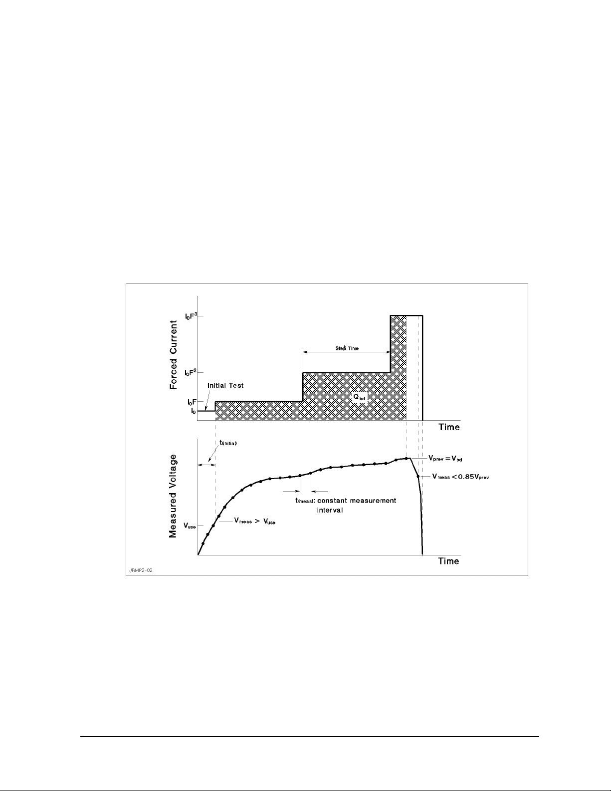
J-Ramp Stress Test
A stepped current is applied to the oxide capacitor, and the voltage across the capacitor is
continuously measured. Normally, applying the current to the oxide capacitor charges up
the capacitor, so the voltage increases across the capacitor. When the electric field reaches
a threshold, the oxide is broken, and current flows through the oxide.
Figure 2-2 shows the concept of Vbd and Qbd for the J-ramp stress test. The forced current
is increased logarithmically, and the voltage across the capacitor is measured at a constant
interval. When the measured voltage < previously measured voltage ´ 0.85, the breakdown
is considered to have occurred in the oxide. The previously measured voltage is considered
to be Vbd, and Qbd is calculated by integrating the current applied to the oxide.
If the measurement results indicate that breakdown occurred, the result of J-ramp stress test
is defined as "fail".
Figure 2-2 Concept of Breakdown Voltage and Charge
J-RAMP
Theory of J-Ramp Test Procedure
Agilent 4155C/4156C Sample Application Programs Guide Book, Edition 1 2-5
Page 46

J-RAMP
Theory of J-Ramp Test Procedure
Step Increase Factor for Forced Current
The current forced to the oxide capacitor is stepped in a logarithmic manner. The value of
each step is related to the initial current I
following equation:
I
= I0 ´ F
n
n
Where n = 1, 2, 3, . . .
That is,
I
= I0 ´ F
1
I
= I0 ´ F
2
I3 = I0 ´ F
2
3
. . . .
I
= I0 ´ F
n
n
J-Ramp Characteristics (Conditions for Forced Current)
The forced current must satisfy the following conditions:
by the step increase factor F as shown in the
0
• Current ramp rate: 1 decade/500 ms.
• Maximum time (t
) between voltage measurements: 50 ms or once per current step,
meas
whichever is less.
• Maximum charge density: 50 C/cm
2
.
• Maximum electric field (voltage compliance limit): 15 MV/cm.
• Maximum current step increase factor F: Ö10
, approximately 3.2.
• Step interval time of applied current: constant.
Indication of faulty J-ramp stress test
If either of the following situations occurs during the J-ramp stress test, the test should be
aborted. This indicates that the testing was faulty.
• Accumulated charge density (q) reaches the maximum allowed charge density. Charge
density q is the accumulated charge Q divided by the oxide area Area.
• Maximum allowed electric field E is reached.
2-6 Agilent 4155C/4156C Sample Application Programs Guide Book, Edition 1
Page 47

J-RAMP
Theory of J-Ramp Test Procedure
Post Stress Test
The post stress test checks the oxide status after the J-ramp stress test. If the oxide is
broken, proper J-ramp stress was applied to the oxide capacitor, and the result of post stress
test is defined as "fail".
To check the oxide status, the initial current (I
) is applied to the oxide capacitor (same as
0
initial test), then the voltage across the capacitor is measured. The measured voltage
(V
) indicates the following:
meas
• If V
meas
< V
use
:
The oxide was broken by the J-ramp stress test. Forced current flows through the oxide,
so the voltage across the capacitor does not increase enough.
• If V
meas
> V
use
:
The oxide was not broken by the J-ramp stress test. Forced current does not flow
through the oxide enough, so the voltage across the capacitor increases.
One possible reason is that the testing was faulty as described in the previous section.
For example, the current was not forced to the oxide due to an open circuit.
Agilent 4155C/4156C Sample Application Programs Guide Book, Edition 1 2-7
Page 48

J-RAMP
Theory of J-Ramp Test Procedure
Failure Categorization and Data Recording
According to the measurement results, the oxide status is categorized as follows:
Initial Failure: Failed the initial test. Indicates initially defective oxide
Catastrophic Failure: Failed during J-ramp and post stress tests. Indicates that
Masked Catastrophic Failure: Did not fail during J-ramp stress test, but failed post
Non-catastrophic Failure: Failed during the J-ramp stress test, but not post stress
Others: Did not fail during J-ramp stress test, and did not fail
The failure category is recorded for each test device. If the catastrophic failure is observed,
breakdown voltage (Vbd) and breakdown charge density (q
recorded.
Table 2-1 shows the oxide failure categories.
capacitor. Other tests should not be performed.
oxide capacitor was properly broken by the J-ramp stress
test.
stress test.
test.
post stress test.
= Qbd/Area) are also
bd
Table 2-1 Oxide Failure Categories
Stress Failure Category Initial Test J-Ramp Stress Test Post Stress Test
Initial Fail n.a. n.a.
Catastrophic
a
Masked Catastrophic Pass Pass Fail
Non-catastrophic Pass Fail Pass
Others Pass Pass Pass
a. Vbd and qbd are also recorded.
Pass Fail Fail
2-8 Agilent 4155C/4156C Sample Application Programs Guide Book, Edition 1
Page 49

J-RAMP
Basic Operation
Basic Operation
This section covers the following for using an 4155/4156 to perform J-Ramp Test: required
equipment, required files, methodology, how to execute the sample program, and sample
program overview.
Methodology
The entire J-Ramp Test procedure can be performed by executing the JRAMP sample
program on the built-in IBASIC controller of the 4155/4156.
As explained in “Theory of J-Ramp Test Procedure”, the J-ramp test consists of three
measurement parts and an analysis part. Each measurement part executes three steps as
follows:
1. Loads the measurement setup file into the 4155/4156 execution environment.
2. Changes some of the measurement or analysis parameters on the setup pages.
3. Executes the measurement.
The JRAMP program executes the above three steps for each test: initial test, J-ramp stress
test, and post stress test. Using the measurement setups (step 1 above) loaded from a file
reduces the length and complexity of the program. For details, see Programmer's Guide.
Measurement setups, which are loaded into the 4155/4156 execution environment, were
previously developed and saved to measurement setup files on the diskette. You can easily
modify the measurement setup information in fill-in-the-blank manner in the 4155/4156
execution environment. The JRAMP sample program is also saved to the diskette. You can
easily modify the sample program by using the editor in the built-in IBASIC environment.
The JRAMP sample program assumes that the built-in IBASIC controller of the 4155/4156
is used, but you can also use another controller such as HP BASIC running on an external
computer. To do so, you must modify the sample program for your environment. See
“Customization” on how to modify the program to run on an external controller.
Agilent 4155C/4156C Sample Application Programs Guide Book, Edition 1 2-9
Page 50

J-RAMP
Basic Operation
Initial Test
The initial test makes sure the oxide capacitor is initially good by applying an initial
current I
capacitor. If the voltage does not reach the normal operating voltage, the oxide capacitor is
categorized as "initial failure".
The sample program assumes that SMU1 and SMU4 are connected to the oxide capacitor
as shown in Figure 2-3.
Figure 2-3 Simplified Measurement Circuit and Output Current of Initial Test
(Iforce0 in the sample program), then measuring the voltage across the oxide
0
For the initial test, the sample program does as follows:
1. Sets up the 4155/4156 according to the JINIT.MES setup file, which the sample
program previously loaded from the diskette into internal memory (MEM1).
2. Sets up SMU1 to constant current Iforce0 for PMOS device, or -Iforce0 for
NMOS device. Iforce0 value is specified at beginning of the sample program, and
reset in the MEASURE: SAMPLING SETUP page by OUTPUT statement (line 2550
of the sample program).
3. Sets the THRESHOLD value of the STOP CONDITION to Vuse or -Vuse, which is
the normal operating voltage that was specified at beginning of the sample program.
4. Forces current Iforce0 from SMU1, and measures as set up by the JINIT.MES file
described next.
5. Checks if the maximum voltage reached Vuse. If not, the sample program aborts
further testing.
2-10 Agilent 4155C/4156C Sample Application Programs Guide Book, Edition 1
Page 51

Basic Operation
y
The following are main points about the setup by the JINIT.MES setup file:
• On CHANNELS: CHANNEL DEFINITION page (see Figure 2-13)
• MEASUREMENT MODE is set to SAMPLING.
• SMU4 is set to be a constant voltage source.
• SMU1 is set to be a constant current source.
• Vg is defined as name of voltage measured by SMU1.
• On MEASURE: SAMPLING SETUP page (see Figure 2-4)
• Sampling mode (MODE) is set to LINEAR.
• Sampling measurement interval (INITIAL INTERVAL) is set to 10 ms.
• NO. OF SAMPLES is set to 100.
J-RAMP
• TOTAL SAMP. TIME is set to 1 second (t
). So, for 1 second, the current
initial
Iforce0 will be forced and sampling measurements will be performed.
• SMU4 is set to force a constant 0 V.
• SMU1 is set to force a constant 1 mA.
• STOP CONDITION is enabled, NAME is set to Vg, and EVENT is set to
|Val|>|Th|. Note that THRESHOLD is set to Vuse by the sample program as
described previously.
So, if the maximum Vg measured by SMU1 reaches Vuse, the sample program
next performs the J-Ramp Stress test. If not, the measurement will abort further
testing.
Figure 2-4 MEASURE: SAMPLING SETUP Page for Initial Test
MEASURE: S AMPLI NG S ETUP 95 FEB0 2 0 9: 20 AM
Samplin g Mode
Interval Time
Number of Samples
Total Sam pling Tim e
Volt age Ramp I ni ti al/ Pos t Spot Measur ement
* SAMPL I NG PARAMETER * STOP CONDI TI ON
MODE LI NEAR ENABLE/ DI SABLE ENABLE
I NI TI AL I NTERVAL 10. 00ms ENABLE DELAY 0. 0000000 s
NO. OF SAMPLES 1 00 NAME Vg
TOTAL SAMP. TI ME 1. 00 s THRESHOL D 4. 0000000 V
HOLD TI ME 0. 000000 s EVENT NO. 1
FI LT ER ON
* CONSTANT
UNI T SMU1: HR S MU4: HR
NAME I g Vs b
MODE I V
SOURCE -1.000uA 0.0000 V ----- ---- ---------
COMPLIANCE 40.000 V 100.00mA ----- ---- ---------
EVENT |Val| > |Th|
Stop cond ition is enab led.
LI NEAR
LOG10
LOG25
LOG50
THINNED
OUT
Variable Name
Threshold V alue
Event
1
LI NEAR
Select Sampling Mode with softkey or rotary knob.
SAMPLNG
SETUP
MEASURE
SETUP
OUT PUT
SEQ
PREV
PAGE
I
NEXT
PAGE
1
This value is re-specified
sample program.
b
Agilent 4155C/4156C Sample Application Programs Guide Book, Edition 1 2-11
Page 52

J-RAMP
Basic Operation
J-Ramp Stress Test
After the initial test, the sample program executes the J-ramp stress test. Logarithmic
stepped current is applied to the oxide, and voltage across the oxide is measured at least
once for each step.
The measurement setup for the J-ramp stress test is stored in the JRMP.MES setup file on
the diskette. At the beginning of the sample program, this setup is loaded into internal
memory (MEM2). Then, at the beginning of the J-ramp stress test, the sample program
loads this setup into the 4155/4156.
To force proper stepped current, the sample program and JRMP.MES set the following:
• SMU channel definition (see Figure 2-5):
SMU1 is set to current sweep mode, and SMU4 is set to force a constant 0 V.
• Constant step interval time (see Figure 2-7):
Step interval time of output sweep current should be constant. The time can be constant
by setting the delay time and step delay time. See Figure 2-7. However in the
logarithmic sweep, if the sweep range extends to 1 decade or more (example; sweep
range 1 mA to 100 mA), the step interval time varies due to the output range changing of
sweep source. This interval time error will cause the calculation error of breakdown
charge (Qbd). Then the JRAMP sample program does the error correction of Qbd after
the measurement.
• Stepped current to be forced:
Stepped current forced to the oxide is increased logarithmically. This stepped current is
defined in the sample program.
• Measurement stop condition:
Current sweep continues until one of three conditions is satisfied.
• Searching for breakdown point and calculating Qbd:
After the measurement, the JRAMP sample program gets the measured voltage values,
and searches for the breakdown voltage (Vbd). Then, calculates Qbd by using the
user-defined functions. Finally, the program compensates the Qbd calculation error,
and displays the Qbd value.
2-12 Agilent 4155C/4156C Sample Application Programs Guide Book, Edition 1
Page 53

SMU channel definition.
The sample program assumes the connection between the SMUs and the oxide capacitor as
shown in Figure 2-5.
The JRMP.MES file sets the following (see Figure 2-6 and Figure 2-9):
• SMU4 is set to force a constant 0 V.
• SMU1 is set to current sweep mode.
• SMU4 is used prevent overcurrent by using its current compliance function.
Compliance is set to 100 mA.
Figure 2-5 Simplified Measurement Circuit of J-Ramp Stress Test
J-RAMP
Basic Operation
Figure 2-6 CHANNELS: CHANNEL DEFINITION Page for J-Ramp Stress Test
CHANNEL S: CHANNE L DEF I NI T I ON
Vol t age Ramp I ni t i al / Post Spot Meas ur emen t
SMU1 and SMU 4
are connected to
the oxide capacitor.
* ME A SU RE ME NT MO DE
SWEEP
* CHANNE L S
MEASURE STBY SERI ES
UNI T VNAME I NAME MODE FCTN RESI STANCE
SMU1:HRVgIgI VAR1 0ohm
SMU2 : HR 0ohm
SMU3 : HR
SMU4: HR Vs b I s b V CONST
VSU1 -------
VSU2 -------
VMU1 ------- ----- ----
VMU2 ------- ----- ----
SMU1 is sweep source (VAR1).
SMU4 is constant source.
.
Agilent 4155C/4156C Sample Application Programs Guide Book, Edition 1 2-13
Page 54

J-RAMP
Basic Operation
Constnt step interval.
To keep a constant step interval time for the current sweep and measurement, triggering
and measurement ranging techniques are used. JRMP.MES sets the measurement ranging
mode to FIXED, so the time between measurements does not vary due to measurement
range changing.
JRMP.MES enables the TRIG OUT function, and the sample program calculates and sets
values so that the step interval time becomes constant as shown in Figure 2-7. The step
interval time (Step_time) is the delay time (Step_delay_t) plus step delay time
(Step_keep_t). Strictly speaking, the sample program calculates these as follows:
Step_time = 0.5 ´ log
(Factor) - 3.7 ms
10
Step_delay_t = Step_time/2 (delay time)
Step_keep_t = Step_time - Step_delay_t (step delay time)
Where,
• 3.7 ms is overhead time associated with the current output logarithmic sweep mode.
So, do not set another value in this field.
• Factor is the step increase factor. See later in this section and “Proof of Equations”
for details of this calculation.
In the logarithmic sweep, if the sweep range extends to 1 decade or more, the step interval
time (Step_time) varies due to the output range changing of sweep source. The output
range changing adds the range changing time to the step interval time. This additional time
depends on the range setting, but it is approximately 2 % of the time for 1 decade sweep.
The output range changing will also cause the calculation error of Qbd. The JRAMP
sample program can compensate this calculation error.
Figure 2-7 Output Sweep Current for J-Ramp Stress Test
2-14 Agilent 4155C/4156C Sample Application Programs Guide Book, Edition 1
Page 55

J-RAMP
Basic Operation
Figure 2-8 MEASURE: MEASURE SETUP and OUTPUT SEQUENCE Pages for J-Ramp
Stress Test
Ranging mode is FIXED.
Trigger setup is ENABLE. Trigger Out Mode
MEASURE: OUTPUT SEQUENCE 95 FEB02 09 : 41AM
Volt age Ramp I ni ti al/ Post Spot Measur ement
MEASURE: MEASURE SETUP 95 FEB02 09 : 40 AM
Volt age Ramp I ni ti al/ Post Spot Measur ement
* MEASUREMENT RANGE
UNI T NAME RANGE ZERO CANCEL OFF
SMU1 : HR Vg FI XED 4 0V OFF
SMU4:HR I sb LI MI TED 1nA OFF [ 10pA]
*INTEG TI ME
TI ME NPLC
SHORT@ 640us 0.032
MED 2 0 . 0 ms 1
LONG 320. ms 16
*WAI T TIME
0 * (DEFAULT WAI T TI ME)
FI XED
Select Range Mode wit h s of t key or rot ary knob.
SWEEP
SETUP
MEA S UR E
SETUP
OUTPUT
SEQ
( *: Ol d dat a i s used. )
PREV
PAGE
MEASURE: MEASURE SETUP Page
AUTO
FI XED
LI MI TED
AUTO
I
NEXT
PAGE
SMU1 : HR
PREV
PAGE
SMU2 : HR
SMU3 : HR
SMU4 : HR
VSU1
VSU2
I
NEXT
PAGE
* TRI GGER SETUP
ENABLE/ DI SABLE ENABLE
FUNCTI ON TRI G OUT
STEP DELA Y 2 5. 0ms
POLARI TY POSI TI VE
ey o r r ot ary knob.
MEASURE: OUTPUT SEQUENCE Page
Agilent 4155C/4156C Sample Application Programs Guide Book, Edition 1 2-15
Page 56

J-RAMP
Basic Operation
Stepped current to be forced.
The sample program sets to force to the oxide a current that increases logarithmically
according to the equation I
the JRAMP sample program, you specify the start current (Iforce0 on line 1800) and
step increase factor F (Factor on line 1890), then the step interval time (Step_time on
line 1900) and stop current (Istop on line 4560) are calculated. For NMOS devices, the
ramp test subprogram actually sets the opposite polarity for these values by using the Tp
variable (lines 2020 and 2030).
= I0 ´ Fn, where n = 1, 2, . . . n. See “J-Ramp Stress Test”. In
n
Iforce0 is normally 1 mA, as mentioned in the “Theory of J-Ramp Test Procedure”.
Three values (10
, 10
1/25
, and 10
1/50
) are possible for step factor F (Factor) of the
1/10
4155/4156 because you can use 10, 25, or 50 steps per decade for the logarithmic sweep.
The step interval time Ts (Step_time in program) of each step depends on the number of
steps per decade, and must satisfy the condition that the ramp rate is 1 decade/500 ms. So,
if N is the number of steps per decade, then Ts = 0.5/N. The following is the relationship of
Ts to the step increase factor F:
Ts = 0.5 ´ log
10
F
The current is stepped logarithmically until the charge density reaches the maximum
allowed value, which is normally 50 C/cm
n
It() td
ò
0
Where, I(t) = I
n
I0FnTsnd×××
ò
0
´ Fn, t = n ´ Ts (time), n is step number, Ts is the step interval time, q
0
q
max
2
Area×==
, as follows:
max
is
the maximum allowed charge density, and Area is the area of the oxide capacitor.
If you solve for n in the equation above, you get the following result:
F10q
1
----------------
n
log
F
10
æö
log×=
èø
10
×log Area×
I
0Ts
max
×
--------------------------------------------------1+
So, the current will be stepped n times to reach the maximum charge density, and the value
of the current (Istop) at that step will be as follows:
I
stopI0
Fn×=
So, the sample program calculates and sets Ts (Step_time) and Istop as described
above.
For details about solving all the above equations above, see “Proof of Equations”.
2-16 Agilent 4155C/4156C Sample Application Programs Guide Book, Edition 1
Page 57

J-RAMP
Basic Operation
Measurement stop condition.
NOTE JEDEC Standard No. 35 specifies that the current sweep should abort when breakdown
occurs, but the JRAMP sample program continues the current sweep until one of the
following three conditions is satisfied:
• Current sweep setting reaches current stop (Istop), which sample program calculates
according to the maximum allowed charge density.
• SMU4 (which is set to force 0 V) reaches current compliance, which is set to 100 mA
by the measurement setup file JRMP.MES.
• SMU1 (which is current sweep source) reaches voltage compliance (Vgcomp), which
the sample program calculates as Max_e*Tox, where Max_e is the maximum
allowed electric field, and Tox is the oxide thickness.
When the voltage across the oxide reaches the voltage compliance setting, the
measurement must stop and current sweep must be aborted. So, SWEEP STOP AT
COMPLIANCE must be set as shown in Figure 2-9.
Figure 2-9 MEASURE: SWEEP SETUP Page for J-Ramp Stress Test
MEASURE: SWEEP SET UP 94 DEC29 0 9: 29 AM
* VARI ABLE VAR1 VAR2
UNIT SMU1:HR
NAME I g
SWEEP MODE SI NGLE
LI N/ LOG LOG 10
START 1. 000uA
STOP 100. 00uA
STEP ---------
NO OF S TE P 2 1
COMPLIANCE 30. 000 V
POWER COMP OFF
*TI MI NG
HOLD TI ME 0. 0000 s
DELAY TI ME 25. 0ms * SWEEP STOP AT COMPLI ANCE St at us
* CONSTANT
UNIT SMU4:HR
NAME Vs b
MOD E V
SOURCE 0.0000 V --------- --------- ---------
COMPLI ANCE 100.00mA --------- --------- ---------
SI NGLE
Selec t Sweep Mode wit h sof t key or r ot ar y knob.
SWEEP
SETUP
MEASURE
SETUP
OUT PU T
SEQ
Sweep aborts at COMPLIANCE.
PREV
PAGE
SI NGLE
DOUBL E
NEXT
PAGE
Agilent 4155C/4156C Sample Application Programs Guide Book, Edition 1 2-17
Page 58

J-RAMP
Tbd
Basic Operation
Searching for breakdown point and calculating Qbd.
The sample program searches for the breakdown point as follows:
When a measured voltage < previous measured voltage ´ 0.85, the previous measured
voltage is defined as the breakdown voltage (Vbd).
To search for Vbd, the sample program stores all the measured voltage values in array
variable Vg, then searches for the first TRUE case of the following, then sets Vbd as
follows:
1. If Vg(2) < Vg(1)*0.85, then Vbd = Vg(1).
2. If Vg(3) < Vg(2)*0.85, then Vbd = Vg(2).
3. If Vg(4) < Vg(3)*0.85, then Vbd = Vg(3).
. . . . . . . . .
99. If Vg(100) < Vg(99)*0.85, then Vbd = Vg(99).
IBASIC programming can easily realize this algorithm.
After finding the breakdown point, the sample program performs analysis on the measured
curve to get Qbd as follows:
1. Displays marker on the curve.
2. Moves the marker to the breakdown point.
3. Calculates Qbd by using a user function.
4. Saves value of Qbd.
The user-defined function calculates Qbd as follows:
n
1
Qbd Ig t() td
==
ò
Tstart
-- 2
i 2=
å
Ig
iIgi 1–
+()TiT
Where, n is step number when the breakdown occurs.
The JRMP.MES setup file defines the user functions on the CHANNELS: USER
FUNCTION DEFINITION page (see Figure 2-21) as follows:
Table 2-2 User Functions for Ramp Stress Test
Name Units Definition
Time sec
0.05 * @INDEX
Vbd V @MY2
Qbdo C INTEG(Ig,Time)
–()×
i 1–
a
Qbd C
b
0
a. This is a temporary definition. Time is redefined by line 2940 of the sample
program.
b. This is a temporary value. Qbd value is entered by line 3590 of the sample pro-
gram.
2-18 Agilent 4155C/4156C Sample Application Programs Guide Book, Edition 1
Page 59

Post Stress Test
Post stress test checks the oxide status after the ramp stress test.
The methodology of the post stress test is the same as for initial test. Initial current
(Iforce0) is applied to the oxide, then the voltage across the oxide capacitor is
measured.
For the measurement circuit, connections, and measurement setups, see “Initial Test”.
Failure Categorization
Table 2-3 shows the oxide failure categories that are determined by the sample program.
The failure category is displayed for each device, and Vbd, Qbd, and qbd are also
displayed.
The measured data and measurement settings are saved in a file.
Table 2-3 Oxide Failure Categories
Category Initial Test Ramp Stress Test Post Stress Test
J-RAMP
Basic Operation
Initial V
Catastrophic V
Masked Catastrophic V
Non-catastrophic V
Other V
meas
meas
meas
meas
meas
< V
use
³ V
useVmeas
³ V
useVmeas
³ V
useVmeas
³ V
useVmeas
n.a. n.a.
< 0.85 ´ V
prev
V
occurs.
< 0.85 ´ V
prev
V
does not occur.
< 0.85 ´ V
prev
V
occurs.
< 0.85 ´ V
prev
V
does not occur.
meas
meas
meas
meas
< V
< V
³ V
³ V
use
use
use
use
Agilent 4155C/4156C Sample Application Programs Guide Book, Edition 1 2-19
Page 60

J-RAMP
Basic Operation
Required Equipment
The following equipment is required to use the J-Ramp sample program:
• 4155 or 4156 Semiconductor Parameter Analyzer
• Two triaxial cables
• Probe station
• This operation manual
• Diskette that contains sample program file and two setup files. See below.
Program Files Required
The following files are used for the J-Ramp test:
JRAMP J-Ramp sample program. This is an IBASIC program file saved in
ASCII format.
JINIT.MES Measurement setup file for initial and post stress test.
JRMP.MES Measurement setup file for J-ramp stress test.
Executing the JRAMP Program
Before executing the program, you may need to customize the program to suit your test
device. See “Customization”.
This procedure describes how to execute the sample program.
1. Display the SYSTEM: MISCELLANEOUS screen, and set the REMOTE CONTROL
COMMAND SET field to 4155/4156.
2. Display the All IBASIC screen by pressing the front-panel
3. Insert a diskette containing the JRAMP program and JRMP.MES file into the built-in
3.5 inch flexible disk drive.
4. Get the JRAMP sample program as follows:
a. Select the GET "" softkey.
b. Enter JRAMP as shown below.
GET"JRAMP"
c. Press the front-panel Enter key.
5. (Optional) Edit the program, and change the measurement conditions. See Table 2-4.
6. Connect test device to the 4155/4156. See Figure 2-3.
7. Press the front-panel
Measurement results similar to the Figure 2-10 will be displayed on the GRAPHICS page
of the 4155/4156.
Run key to execute the program.
Display key twice.
2-20 Agilent 4155C/4156C Sample Application Programs Guide Book, Edition 1
Page 61
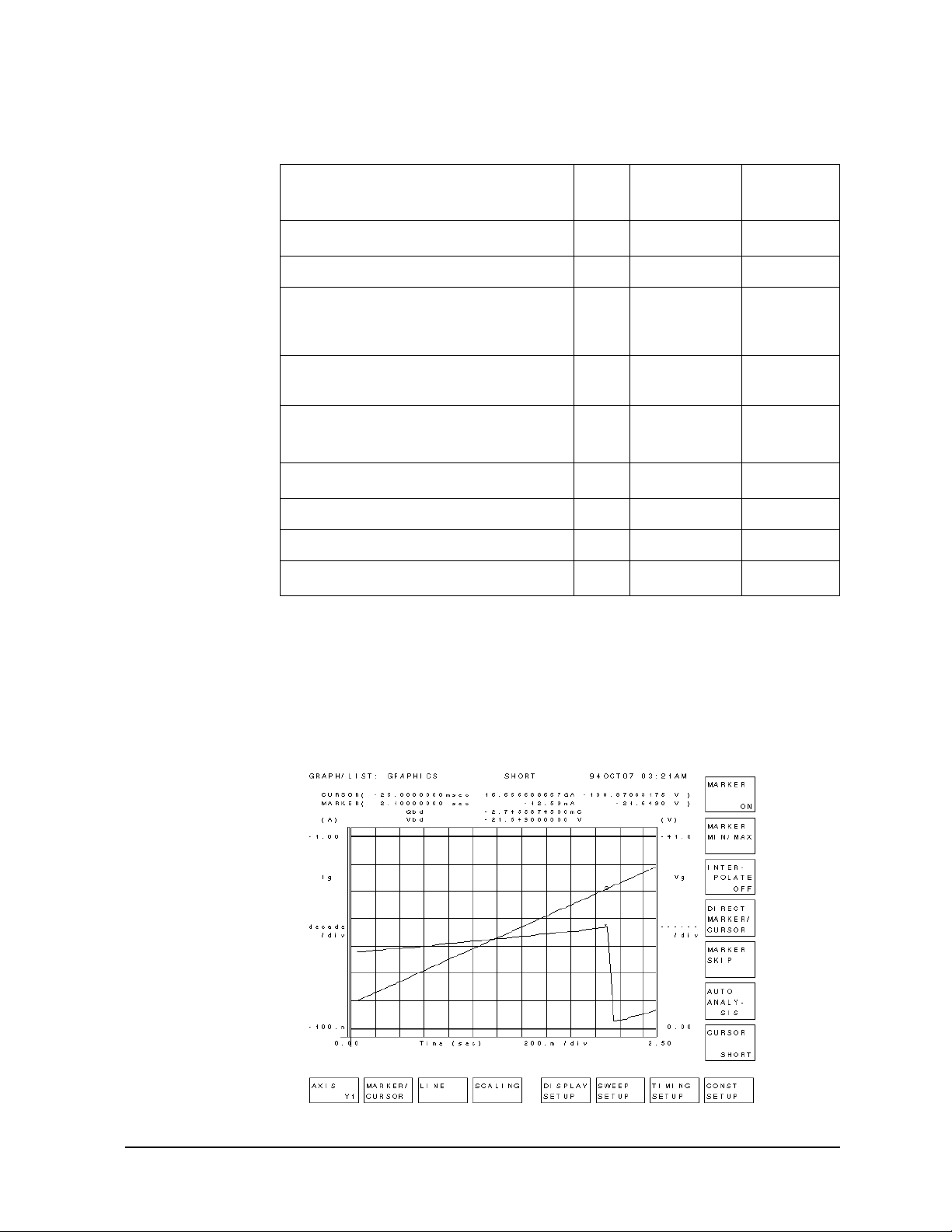
Table 2-4 JRAMP Sample Program Setup Parameters
J-RAMP
Basic Operation
Parameter
Line
No.
Device Type (NMOS or PMOS) 1790
Variable
Name
Type$
Default
Valu e
a
NMOS
Initial current or sweep start current (A) 1800 Iforce0 1.E-6
Normal operating voltage for the device (V)
1810 Vuse 5
(threshold value used for Initial Test/Post
Test)
Type of SMU used for current sweep source
1820
Smu_type
b
1
(1: HRSMU, 0: MPSMU or HPSMU)
Ramp step increase factor 10
1/50
10
Maximum charge (C/cm2)
, 10
1/25
1890 Factor
, or
1940 Max_q 50
10
1/10
1/10
Maximum electric field (V/cm) 1950 Max_e 15*1.E+6
Thickness of oxide (cm) 1970 Tox 130*1.E-8
Area of oxide capacitor (cm
2
)
1980 Area 0.001
a. If type is NMOS, opposite polarity values for some of the values are actually
used later in the program by using the Tp parameter, which is set to -1 in line
2030.
b. If you use the 4155, or MPSMU in the 41501 Expander, change the value to 0.
If you use the HPSMU in the 41501, use the JRAMP1 sample program. See
“When SMU Lacks Power to Break Oxide”.
Figure 2-10 An Example of Measurement Results
Agilent 4155C/4156C Sample Application Programs Guide Book, Edition 1 2-21
Page 62

J-RAMP
Basic Operation
Flowchart of Sample JRAMP Program
Figure 2-11 shows flowchart of sample JRAMP program and corresponding subprogram
names.
Figure 2-11 Flowchart of Sample JRAMP Program
2-22 Agilent 4155C/4156C Sample Application Programs Guide Book, Edition 1
Page 63

J-RAMP
Basic Operation
The following provides a brief description for each subprogram.
Test_setting Specifies and checks the parameter values. These are values that the
program will set directly instead of some of the setup file values. This
subprogram calls the Calc_istop subprogram to calculate the
sweep stop current value.
Get_file Loads measurement setup files from the diskette into internal memory:
initial/post measurement setup into MEM1, and sweep measurement
setup into MEM2. Having the measurement setups in internal memory
reduces the measurement time.
Init_fin_test Executes initial test or post stress test. First parameter specifies the
test: Init is for initial test, and Fin is for post stress test. The
measurement results are returned to the second parameter.
Judge Categorizes failure according to measurement results of initial, ramped
stress, and post stress tests. If the failure is initial failure, this
subprogram aborts the program.
Ramp_test Executes sweep measurement for ramped stress test. After the
measurement, compensates the Qbd value using the FNCompen
function, and displays Vbd, Qbd, and qbd values. The measurement
result data is temporarily stored in internal memory (MEM3).
Save_data Saves measurement result data (in MEM3) to a file on the diskette.
Calc_istop Calculates the sweep stop current value from the start current
(Iforce0) and ramp step increase factor (Factor).
FNCompen Compensates the Qbd calculation error caused by the sweep source
output range changing.
Agilent 4155C/4156C Sample Application Programs Guide Book, Edition 1 2-23
Page 64

J-RAMP
Customization
Customization
This section describes how to customize the sample program to suit your test device.
Using an External Computer
This sample program (JRAMP) is assumed to run on the Instrument BASIC that is built
into the 4155/4156. The 4155/4156 is used as both the measurement instrument and the
controller running IBASIC, so JRAMP sets device selector 800. On the following three
lines, the 4155/4156 is assigned and interrupt from it is enabled as follows:
1450 ASSIGN @Hp4155 TO 800
1530 ON INTR 8 CALL Err_check
1540 ENABLE INTR 8;2
:
If you use an external controller (that can run HP BASIC environment) to control the
4155/4156, you need to modify a few lines of the sample program. For example, if you use
HP BASIC/WS on an HP 9000 Series 300 computer, you only need to modify lines the
above three lines as follows:
In this case, the 4155/4156 has GPIB address 17 and is not used as the system controller,
and is connected to the built-in GPIB of the HP 9000 series 300 controller with an GPIB
cable. Use the following procedure to set the GPIB address and system mode:
1. Turn on your 4155/4156.
2. Press the front-panel
System key.
3. Select the MISCELLANEOUS softkey.
4. Move the field pointer to the "415x is " field, then select NOT CONTROLLER softkey.
5. Move the field pointer to the "415x" field in the GPIB ADDRESS area, then enter: 17
Enter.
2-24 Agilent 4155C/4156C Sample Application Programs Guide Book, Edition 1
Page 65

J-RAMP
Customization
SYSTEM: MI SCELL ANEOUS 99 DEC10 0 4 : 42 PM
* 41 56 B i s * POWER L I NE FREQUENCY
System Mode
GPIB Address
NOT S YS T EM CONT ROL L E R 50 H z
* GPI B ADDRESS *414156B NETWORK SETUP
4156B 17 HOST NAME
HARD COPY 1 I P A DDRES S 0 . 0. 0. 0
* REMOT E CONT ROL GROU P I D 1 0 0
COMMAND SET 4155/ 56
*CLOCK TEXT OUT -h
YMDHM GRAPHOUT-h-l
19 99 1 2 10 16 4 2 SERVER T YPE BSD
*SYSTEM SETUP *NETWORK DRI VE SETUP
BEEP ON LABEL
SCREEN SAVE 30 mi n I P ADDRESS 0. 0. 0. 0
LP TI MEOUT 300 s ec DI RECTORY /
NOT SYSTEM CONTROLLER
Sel ect Syst em Cont r ol Mode wi t h sof t key or r ot ar y knob.
FI LER MI SCEL-
LANEOUS
CONFI G CAL I B/
Specifying Setup File to Load
USER I D 200
* NETWORK PRI NTER SETUP
PRI NTER
IP ADDRESS 0.0.0.0
DI AG
PRI NT
SETUP
COLOR
SETUP
CON-
TROLLER
NOT
CON-
TROLLER
Two setup files are used to set up the 4155/4156 for the J-Ramp test: one is used for initial
and post stress tests, and the other is for ramp stress test.
Filenames of these setups are defined on the following lines:
1740 Init_file$="JINIT.MES" !Init/Post Measurement Setup File Name
1750 Sweep_file$="JRMP.MES" !Ramp Setup File Name
If you want to use other setup files, store the setup files on the diskette, then modify the
filenames on the lines above.
File for Saving Measurement Results
The following lines specify the filename for the measurement results file. The filename
starts with "D", then HHMMS, then ends with ".DAT". Where HH is hour, MM is minute,
and S is second (tens digit only).
1760 Save_file$=TIME$(TIMEDATE) !File Name for saving measurement
results
1770 Save_file$="D"&Save_file$[1,2]&Save_file$[4,5]&Save_file$[7,7]&
".DAT"
The following line commands the 4155/4156 to create the specified file on the diskette,
then stores the result data in the file.
4120 OUTPUT @Hp4155;":MMEM:STOR:TRACDEF,'"&Save_file$&"','DISK'"
For example, "D09344.DAT" file that contains measurement data is created on the
diskette. This filename means the "data file created at 9:34 4x seconds."
To change to your desired filename, you only need to edit line 1770.
Agilent 4155C/4156C Sample Application Programs Guide Book, Edition 1 2-25
Page 66

J-RAMP
Customization
Setting up Input Parameters
Input parameter values are specified on the following lines. These are values that the
sample program will set directly instead of using some of the setup file values. You can
easily modify the values by editing these program lines.
1790 Type$="NMOS" !DevtypeNMOS-Pbulk,PMOS-Nbulk
1800 Iforce0=1.E-6 !Initial current (A)
1810 Vuse=5 !Vuse (V) (Reference for Init/Post test)
1820 Smu_type=1 !SMU type used
1830 !0:MP/HPSMU
1840 !1:HRSMU
1850 !--------------------------------------------------1860 !Allowable current factor:
1870 !10^(1/10), 10^(1/25), 10^(1/50)
1880 !--------------------------------------------------1890 Factor=10^(1/10) !Current factor
1900 Step_time=.5/(1/LGT(Factor))-.0037 !Ramp step time
1910 Step_delay_t=Step_time/2 !Step Delay time
1920 Step_keep_t=Step_time-Step_delay_t !Step keep time
1930 !
1940 Max_q=50 !Maximum charge (C/cm^2)
1950 Max_e=15*1.E+6 !Maximum Field (V/cm)
1960 !
1970 Tox=130*1.E-8 !Oxide Thickness (cm)
1980 Area=.001 !Area of oxide capacitor (cm^2)
1990 Calc_istop !Calculate Istop (A)
2000 Vgcomp=Max_e*Tox !Vg compliance (V)
2010 Igcomp=.1 !Ig compliance (A)
Parameter Default Description
Type$
a
NMOS Bulk type: NMOS is for P bulk and PMOS is for N
bulk
Iforce0 1 (mA) Initial current
Vuse 5 (V) Normal operating voltage for the device
b
Smu_type
1 Type of SMU used for current sweep source
(1: HRSMU, 0: MPSMU or HPSMU)
Factor
Max_q
1/10
10
50 (C/cm
2
)
Ramp step increase factor F
1/10
(10
,10
1/25
,or10
1/50
)
Maximum charge density
Max_e 15 (MV/cm) Maximum electric field
Tox
Area
1.30*10
0.001 (cm
-6
(cm)
2
Thickness of oxide
Area of oxide capacitor
)
a. If type is NMOS, opposite polarity values for some of the values are actually
used later in the program by using the Tp parameter, which is set to -1 in line
2030.
b. If you use the 4155, or MPSMU in the 41501 Expander, change the value to 0.
If you use the HPSMU in the 41501, use the JRAMP1 sample program. See
“When SMU Lacks Power to Break Oxide”.
2-26 Agilent 4155C/4156C Sample Application Programs Guide Book, Edition 1
Page 67

When SMU Lacks Power to Break Oxide
You may encounter that the oxide does not break using MPSMU or HRSMU. Because
voltage enough to break the oxide is not forced when relatively high current is forced.
MPSMU or HRSMU can force maximum 20 V with the range of 40 mA through 100 mA.
To solve this problem, you can use HPSMU which is in the 41501 Expander. The HPSMU
can force maximum 100 V with the range of 50 mA through 125 mA.
The following program and setup files assume to perform J-Ramp Test using an HPSMU
and an SMU. Figure 2-12 shows the connections between SMUs and a DUT.
JRAMP1 J-Ramp sample program with HPSMU. This is an IBASIC program
file saved in ASCII format.
JINIT1.MES Measurement setup file for initial and post stress test with HPSMU.
JRMP1.MES Measurement setup file for J-ramp stress test with HPSMU.
Note that you may need to customize the JRAMP1 program and JINIT1.MES and
JRMP1.MES setup files for your application before execution.
Figure 2-12 Simplified Measurement Circuit of J-Ramp Test With HPSMU
J-RAMP
Customization
Agilent 4155C/4156C Sample Application Programs Guide Book, Edition 1 2-27
Page 68

J-RAMP
Measurement Setups
Measurement Setups
This section covers the measurement setups that are stored in the JINIT.MES and
JRMP.MES files.
Setups for Initial and Post Stress Tests
The measurement setups stored in JINIT.MES are used for the initial and post stress tests.
The setups of each page are shown in Figure 2-13 to Figure 2-19.
Setups for Ramped Stress Test
The measurement setups stored in JRMP.MES are used for the ramped stress test. The
setups of each page are shown in Figure 2-20 to Figure 2-26.
2-28 Agilent 4155C/4156C Sample Application Programs Guide Book, Edition 1
Page 69

Measurement Setups
V
Figure 2-13 CHANNELS: CHANNEL DEFINITION Page for Initial/Post Stress
CHANNEL S : CHANNEL DEF I NI T I ON 95 FE B0 2 0 9 : 1 9 AM
Vol t ag e Ramp I ni t i al / Post Spot Measur ement
* MEA SUREMENT MODE
SAMPL I NG
* CHA NNE L S
UNI T VNAME I NAME MODE FCTN RESI ST ANCE
SMU1: HR Vg I g I CONST 0 oh m
SMU2: HR 0 oh m
SMU3: HR
SMU4: HR Vs b I s b V CONST
VSU1 -------
VSU2 -------
VMU1 ------ - ----- ----
VMU2 ------ - ----- ----
SAMPL I NG
Sel ect Measur ement Mode wi t h sof t k ey or r ot ar y knob.
CHANNEL
DEF
USER
FCTN
ME A S U R E S T B Y S E R I E S
USER
VAR
J-RAMP
SWEEP
SAM-
PLI NG
DEF A UL T
MEA S URE
SETUP
ME M1 M
B- T r
VCE- I C
ME M2 M
FET
VDS- I D
ME M3 M
FET
VGS- I D
ME M4 M
DI ODE
VF- I F
I
NEXT
PAGE
Figure 2-14 CHANNELS: USER FUNCTION DEFINITION Page for Initial/Post Stress
CHANNEL S: USER F UNCT I ON DEF I NI T I ON 9 5 F EB 0 2 0 9 : 1 9 AM
Vol t age Ramp I ni t i al / Post Spot Measur ement
* USE R F UNCT I ON
NAME UNI T DE F I NI T I ON
Vm V @MY1
m
E n t e r U s e r F u n c t i o n N a me . ( ma x 6 c h a r s . )
CHANNEL
DEF
USER
FCTN
USER
VAR
PREV
PAGE
DEL ET E
ROW
I
NEXT
PAGE
Agilent 4155C/4156C Sample Application Programs Guide Book, Edition 1 2-29
Page 70

J-RAMP
A
Measurement Setups
Figure 2-15 MEASURE: SAMPLING SETUP Page for Initial/Post Stress
MEASURE: SAMPL I NG SETUP 9 5F EB02 0 9 : 2 0 AM
Vol t age Ramp I ni t i al / Post Spot Measur ement
* SAMPLI NG PARAMETER * ST OP CONDI TI ON
MODE L I NEAR ENABLE/ DI SABL E ENABL E
I NI TI AL I NTERVAL 10. 00ms ENABLE DELAY 0. 0000000 s
NO. OF SAMPLES 1 00 NAME Vg
TOTAL SAMP. TI ME 1. 00 s THRESHOLD 4. 0000000 V
HOLD TI ME 0. 000000 s EVENT NO. 1
FI L TER ON
* CONSTANT
UNI T SMU1 : HR S MU4 : HR
NAME I g Vs b
MOD E I V
SOURCE - 1 . 0 0 0 u A 0 . 0 0 0 0 V - - - ------ ---------
COMPLI ANCE 40. 000 V 100. 00mA - - - ------ ---------
L I NEAR
Sel ect Sampl i ng Mode wi t h sof t key or r ot ar y knob.
SAMPL NG
SETUP
MEASURE
SETUP
OUT PU T
SEQ
EVENT | Va l | > | Th |
PREV
PAGE
L I NEAR
LOG10
LOG25
LOG50
THI NNED
OUT
I
NEX T
PAGE
Figure 2-16 MEASURE: MEASURE SETUP Page for Initial/Post Stress
MEASURE: MEASURE SETUP 95FEB02 09: 20AM
Vol t age Ramp I ni t i al / Post Spot Measur ement
* MEAS UREMENT RANGE
UNI T NAME RANGE Z ERO CANCE L OF F
SMU1:HR Vg AUTO ----- OFF
SMU4: HR I sb LI MI TED 1nA OFF [ 10pA]
*I NTEG TI ME
SHORT@ 640us 0. 032
ME D 2 0 . 0 ms 1
LONG 320. ms 16
*WAI T TI ME
UTO
Sel ect Range Mode wi t h sof t key or rot ar y knob.
SAMPL NG
SETUP
TI ME NPLC
1*(DEFAULTWAITTIME)
MEASURE
SETUP
OUT PU T
SEQ
( *: Ol d dat a i s used. )
PREV
PAGE
AUTO
FI XED
LI MI TED
AUTO
I
NEX T
PAGE
2-30 Agilent 4155C/4156C Sample Application Programs Guide Book, Edition 1
Page 71

Figure 2-17 MEASURE: OUTPUT SEQUENCE Page for Initial/Post Stress
J-RAMP
Measurement Setups
MEASURE: OUTPUT SEQUENCE 95FEB02 09: 21AM
Vol t age Ramp I ni t i al / Post Spot Measur ement
* OUTP UT SE QUENCE * T RI GGER SE T UP
UNIT NAME MODE ENABLE/DISABLE DISABLE
1 SMU4: HR Vs b V FUNCTI ON TRI G OUT
2 SMU1: HR I g I STEP DELAY 0. 000 s
3 SMU2 : HR P OLA RI T Y POSI TI V E
4SMU3:HR
5VSU1
6VSU2
* OUTP UT SE QUENCE MODE
OF S A MP L I NG
SI MULTANEOUS
SMU4 : HR
Sel ect Output Sequence with softkey or rotary knob.
SAMPL NG
SETUP
MEASURE
SETUP
OUT PU T
SEQ
PREV
PAGE
SMU1 : HR
SMU2 : HR
SMU3 : HR
SMU4 : HR
VSU1
VSU2
I
NEXT
PAGE
Figure 2-18 DISPLAY: DISPLAY SETUP Page for Initial/Post Stress
DI SPL AY: DI SP LAY SET UP 9 5F EB02 0 9 : 2 1 AM
Vol t age Ramp I ni t i al / Post Spot Measur ement
*DI SPLAY MODE
GRA P H I CS
*GRAPHI CS
NAME @T I ME Vg
SCALE L I NEAR L I NEAR
MI N 0. 000000000 s - 110. 000mV
MAX 1. 00000 s - 100. 000mV
* GRI D * L I NE PARAMET ER
ON ON
* DATA VARI ABL ES
Vm
GRAPHI CS
Sel ect Di spl ay Mode wi t h sof t key or r ot ar y knob.
DI SPL AY
SETUP
Xaxi s Y1axi s Y2axi s
ANLYSI S
SETUP
PREV
PAGE
GRA P H -
ICS
LI ST
I
NEXT
PAGE
Agilent 4155C/4156C Sample Application Programs Guide Book, Edition 1 2-31
Page 72

J-RAMP
M
M
M
M
Measurement Setups
Figure 2-19 DISPLAY: ANALYSIS SETUP Page for Initial/Post Stress
DI SPL AY: ANAL YSI S SET UP 95 FEB0 2 0 9 : 2 1AM
Vol t age Ramp I ni t i al / Post Spot Me asur ement
*LI NE1:[ ]
*LI NE2:[ ]
* MARKER: At a p o i n t wh er e
[ Vg ] = [ MAX( Vg) ]
[]
*Interpol ate:[OFF]
Sel ect Li ne Mode wi t h s of t key or r ot ar y knob.
DI SPL AY
SETUP
ANLYSI S
SETUP
PREV
PAGE
NORMA L
GRA D
TANGENT
REGRES -
SI ON
DI SABL E
I
NEXT
PAGE
Figure 2-20 CHANNELS: CHANNEL DEFINITION Page for Ramped Stress
CHANNEL S: CHANNEL DEF I NI T I ON 98 OCT2 9 0 1 : 3 4PM
Vol t age Ramp I ni t i al / Post Spot Meas ur ement
* ME A S U R E ME NT MOD E
SWEEP
* CHANNEL S
UNI T VNAME I NAME MODE F CT N RESI ST ANCE
SMU1: HR Vg I g I VAR1 0 o hm
SMU2: HR 0 oh m
SMU3: HR
SMU4:HR Vsb Isb V CONST
VSU1 ------VSU2 ------VMU1 ------- ----- ---VMU2 ------- ----- ----
SWEEP
Sel ec t Measur ement Mode wi t h sof t k ey or r ot ar y knob.
CHANNE L
DEF
USER
FCTN
MEASURE STBY SERI ES
USER
VAR
SWEEP
SAM-
PL I NG
DEF AUL T
MEASURE
SETUP
ME M1
B- T r
VCE- I C
ME M2
FET
VDS- I D
ME M3
FET
VGS- I D
ME M4
DI ODE
VF- I F
B
NEXT
PAGE
2-32 Agilent 4155C/4156C Sample Application Programs Guide Book, Edition 1
Page 73

Measurement Setups
Figure 2-21 CHANNELS: USER FUNCTION DEFINITION Page for Ramped Stress
CHANNELS: USER FUNCTI ON DEFI NI TI ON 9 8 OCT29 0 1 : 32 PM
Vol t age Ramp I ni t i al / Post Spot Meas ur ement
* USER F UNCTI ON
NAME UNIT DEFINITION
Ti me s e c @I NDEX* . 0486
Vb d V @MY 2
Qbdo C I NTEG( I g, Ti me)
Qb d C 0
Ti me
Ent er User Funct i on Name. ( max 6 c har s. )
CHANNE L
DEF
USER
FCTN
USER
VAR
PREV
PAGE
J-RAMP
DEL E T E
ROW
B
NEXT
PAGE
Figure 2-22 MEASURE: SWEEP SETUP Page for Ramped Stress
M EASURE: SWEEP SETUP 98OCT30 11: 19AM
Vol t age Ramp I ni t i al / Pos t Spot Measur ement
* VARI ABLE VAR1 VAR2
UNI T SMU1 : HR
NAME I g
SWEEP MODE SI NGL E
LI N/ LOG LOG 10
START 1. 0000uA
STOP 100. 00uA
STEP --------NO OF ST EP 2 1
COMPLI ANCE 30. 000 V
POWER COMP OFF
*TI MI NG
HOLD TI ME 0. 0000 s
DELAY TI ME 25. 0ms * SWEEP STOP AT COMPL I ANCE St a t u s
* CONSTANT
UNI T SMU4 : HR
NAME Vs b
MOD E V
SOURCE 0.0000 V --------- --------- --------COMPLI ANCE 100. 00mA - - - - - ---- --------- ---------
SI NGL E
Sel ec t Sweep Mode wi t h sof t key or r ot ar y knob.
SWEEP
SETUP
MEASURE
SETUP
OUT P UT
SEQ
PREV
PAGE
SI NGL E
DOUBL E
B
NEXT
PAGE
Agilent 4155C/4156C Sample Application Programs Guide Book, Edition 1 2-33
Page 74

J-RAMP
Measurement Setups
Figure 2-23 MEASURE: MEASURE SETUP Page for Ramped Stress
MEASURE: MEASURE SETUP 9 8 OCT3 0 1 1: 1 9 AM
Vol t age Ramp I ni t i al / Post Spot Meas ur ement
* MEASUREMENT RANGE
UNI T NAME RANGE Z E RO CA NCEL OFF
SMU1: HR Vg FI XED 4 0V OFF
SMU4:HRIsb LIMITED1nA OFF [ 10pA]
AUTO
FI XED
LI MI TED
AUTO
*INTEG TI ME
(*:Ol d data is used.)
TI ME NPLC
SHORT@ 640us 0. 0384
MED 16. 7ms 1
LONG 266* ms 16
*WAI T TI ME
0 * ( DEFAUL T WAI T TI ME)
FI XED
Sel ec t Range Mode wi t h sof t key or r ot ar y k nob.
SWEEP
SETUP
MEASURE
SETUP
OUT PUT
SEQ
Figure 2-24 MEASURE: OUTPUT SEQUENCE Page for Ramped Stress
MEASURE: OUTPUT SEQUENCE 95FEB02 09: 41AM
Vol t age Ramp I ni t i al / Post Spot Measur ement
* OUTP UT SE QUENCE * T RI GGER SE T UP
UNIT NAME MODE ENABLE/DISABLE ENABLE
1 SMU4: HR Vs b V FUNCTI ON TRI G OUT
2 SMU1 : HR I g I STEP DELAY 2 5 . 0 ms
3 SMU2 : HR P OLA RI T Y POSI TI V E
4SMU3:HR
5VSU1
6VSU2
PREV
PAGE
B
NEXT
PAGE
SMU1 : HR
SMU2 : HR
SMU3 : HR
SMU4 : HR
VSU1
VSU2
SMU4 : HR
Sel ect Output Sequence with softkey or rotary knob.
SWEEP
SETUP
MEASURE
SETUP
OUT PU T
SEQ
PREV
PAGE
I
NEX T
PAGE
2-34 Agilent 4155C/4156C Sample Application Programs Guide Book, Edition 1
Page 75

Figure 2-25 DISPLAY: DISPLAY SETUP Page for Ramped Stress
J-RAMP
Measurement Setups
DI SPL AY: DI SP LAY SET UP 9 5F EB02 0 9 : 4 1 AM
Vol t age Ramp I ni t i al / Post Spot Measur ement
*DI SPLAY MODE
GRA P H I CS
*GRAPHI CS
NAME T i me I g V g
SCALE L I NEAR L OG LI NEAR
MI N 0. 0000000 sec 1. 00000000uA 0. 000000000 V
MAX 5. 0000000 sec 100. 0000000mA 30. 000000 V
* GRI D * L I NE PARAMET ER
ON ON
* DATA VARI ABL ES
Vb d
Qb d
GRAPHI CS
Sel ect Di spl ay Mode wi t h sof t key or r ot ar y knob.
DI SPL AY
SETUP
Xaxi s Y1axi s Y2axi s
ANLYSI S
SETUP
PREV
PAGE
GRA P H -
ICS
LI ST
I
NEXT
PAGE
Figure 2-26 DISPLAY: ANALYSIS SETUP Page for Ramped Stress
DI SPL AY: ANAL YSI S SET UP 95 FEB0 2 0 9 : 4 1AM
Vol t age Ramp I ni t i al / Post Spot Measur ement
*LI NE1:[ ]
*LI NE2:[ ]
* MARKER: At a p o i n t wh er e
[Vg ] = [MAX(Vg) ]
[]
*Interpol ate:[OFF]
Sel ect Li ne Mode wi t h s of t key or r ot ar y knob.
DI SPL AY
SETUP
ANLYSI S
SETUP
PREV
PAGE
NORMA L
GRA D
TANGENT
REGRES -
SI ON
DI SABL E
I
NEXT
PAGE
Agilent 4155C/4156C Sample Application Programs Guide Book, Edition 1 2-35
Page 76

J-RAMP
Proof of Equations
Proof of Equations
This section provides the information on how to solve the equations given in “J-Ramp
Stress Test” on page 2-5.
Step Increase Factor (F)
N steps per decade (N = 10, 25, or 50) gives the following equation:
10 ´ I
= I0 ´ F
0
Solving for F gives the following:
N
10 = F
log1010 = log10F
1 = N ´ log10F
N
N
1/N = log
F = 10
So F can be one of the following: 10
1/N
10
F
1/10
, 10
1/25
, or 10
1/50
. In the JRAMP sample program,
F is specified by the Factor variable.
Step Time (Step_time)
Relation between N (steps per decade) and F (step increase factor) is:
N
10 = F
log1010 = log10F
N
1 = N ´ log10F
N = 1 / log
F
10
So,
Step_time
0.5
-------
0.5
---------------- 0 . 5 F
N
1
---------------log
10
F
log´== =
10
The sample program sets N (Fact$) according to the F (Factor) that is set.
Current Stop Value (Istop)
The forced current I is a function of time t, so the accumulated charge to the oxide is:
n
It() td
ò
0
Where, I(t) = I
n
I0FnTsnd×××
ò
0
´ Fn, t = n ´ Ts (time), n is step number, Ts is step time.
0
q
max
Area×==
2-36 Agilent 4155C/4156C Sample Application Programs Guide Book, Edition 1
Page 77

J-RAMP
Proof of Equations
You want to solve to find the step number (n) of the step when the maximum allowed
charge density is reached:
n
I0FnTsnd×××
ò
0
n
I
0Ts
I0T
Fnnd×
×× q
ò
0
1
---------------- Fn[]
×× q
s
log
10
q
Area×=
max
Area×=
max
n
F
0
max
Area×=
I0Ts×
---------------log
Fn1–
n
F
nF
n
10
log×
F
F
q
max
--------------------------------------------------1+=
10
1
---------------log
10
n
1–()q
q
Area F
max
--------------------------------------------------=
I
Area F
×
I
0Ts
n
log=
log×=
F
10
Area×=
max
log××
10
×
0Ts
log××
10
q
Area F
max
æö
--------------------------------------------------1+
èø
10
q
max
æö
--------------------------------------------------1+
èø
log××
10
×
I
0Ts
Area F
log××
10
×
I
0Ts
So, Istop is as follows, where M is the minimum integer that satisfies M ³ n. In the JRAMP
sample program, M is the Step_n variable:
Istop = I
0
´ F
M
NOTE Assuming "y= ax, a: constant", you can get the following:
log y = log a
x
= x ´ log a
(log y)’ = log a
y’ ´ 1/y = log a
y’ = (log a) ´ y = (log a) ´ a
x
So, the integration of ax is:
x
----------- xd
ò
y¢
alog
a
ò
1
----------- y¢()xd
ò
alog
1
-----------
alog
y×
x
a
---------- -== ==
alog
The result of this integration is used to go from 2nd to 3rd step of above solution
(integration of Fn).
Agilent 4155C/4156C Sample Application Programs Guide Book, Edition 1 2-37
Page 78

J-RAMP
Proof of Equations
2-38 Agilent 4155C/4156C Sample Application Programs Guide Book, Edition 1
Page 79

3SWEAT
Page 80

SWEAT
SWEAT means Standardized Wafer-level Electromigration Accelerated Test, which is an
accelerated electromigration test for microelectronic metallization on the wafer.
This test can quickly provide data for monitoring metal reliability and process consistency.
This operation manual describes a sample SWEAT program running on the 4155/4156, and
how to use and customize the program. The program is written in the Instrument BASIC
(IBASIC), and is ready to run on the built-in IBASIC controller of the 4155/4156.
“SWEAT” describes the SWEAT procedure and terminology.
“Basic Operation” describes the SWEAT methodology using the 4155/4156, how to
execute the sample program, and program overview.
“Customization” describes the customization procedure. This procedure is very important
because you probably need to modify the program to suit your test device.
“Setup files” shows the 4155/56 page settings that are stored in the setup files.
3-2 Agilent 4155C/4156C Sample Application Programs Guide Book, Edition 1
Page 81

SWEAT
This section describes the SWEAT procedure (based on the proposed JEDEC 4-June-92
standard) and related terminology.
Overview
SWEAT evaluates sensitivity of metal lines to failure caused by electromigration.
Figure 3-1 shows the flow of the SWEAT test according to the JEDEC proceeding titled "A
PROCEDURE FOR EXECUTING SWEAT" (4-Jun-92).
Figure 3-1 SWEAT Algorithm Flow
SWEAT
SWEAT
First, the initial structure resistance is measured. If it is too high, the program finishes.
If initial structure resistance is within limits, the stress/resistance measurement loop is
performed, which is the part inside the dotted square in Figure 3-1. This loop is a feedback
control loop that does the following:
Agilent 4155C/4156C Sample Application Programs Guide Book, Edition 1 3-3
Page 82

SWEAT
SWEAT
1. An initial current is forced through the test structure, and the calculated time to failure
(CTTF) is calculated by using Black's equation. The current is adjusted in a feedback
loop until the CTTF is within a desired range (TTTF ± Errband), where TTTF is the
target time-to-failure. This feedback period to reach the desired range is called the
settling period. The structure resistance is measured when CTTF becomes within
TTTF ± Errband. This is called the settling resistance.
2. After settling, the current is continuously forced to the test structure. By continuously
adjusting the current, CTTF is forced to track TTTF. This period is called the hold
period. This adjustment is performed by the same feedback control algorithm as used
during the settling period. Gradually, the structure resistance increases due to
electromigration voids (CTTF deviates from TTTF).
The hold period continues until the structure resistance is 1.5 ´ settling resistance. This
means the structure has ruptured (failed).
Input Parameters
Following table shows the input parameters required for the SWEAT procedure and the
values used in the sample program. You can change these values to suit your device.
Input Parameter
(Default Value)
Tcr (2.E-3 °K
-1
)
Temperature coefficient of resistance (This value should be measured before
Description
performing the SWEAT evaluation.) See JEDEC No.33 Standard Method for
Measuring and Using the Temperature Coefficient of Resistance to Determine
the Temperature of a Metallization Line for how to measure TCR.
Rinitfail (1000 W) Maximum allowable structure resistance during the initial resistance test.
Tttf (190 sec) Target time to failure.
Ttt (1000 sec) Total testing time. Testing stops if this time is reached.
Troom (298 °K) Room temperature.
Vcomp (20 V) Voltage compliance.
Isrc_max (1 A) Maximum limit of current source.
Errband (2 sec) Allowable difference between CTTF and TTTF during feedback control loop.
If difference is greater than this value, forced current is adjusted.
Area (1E-8 cm
2
)
Jstart (1.0E-2/Area A/cm
Acc (1.E+10 sA
2
/cm4)
Cross sectional area of the narrowest region of the structure.
2
Starting current density.
)
Acceleration factor for Black's Equation.
Blk (2) Current density factor (n) for Black's Equation.
Ea (0.6 eV) Activation energy for the metallization for Black's Equation.
3-4 Agilent 4155C/4156C Sample Application Programs Guide Book, Edition 1
Page 83

SWEAT
SWEAT
Initial Resistance (Rinit) Measurement
Rinit is the structure resistance at room temperature and low current density.
The algorithm assumes that the ambient temperature is 298 °K and the current density is
sufficiently low so that Joule heating is negligible. Actual Rinit is measured when voltage
(small enough not to cause the Joule heating) is applied to the structure.
CTTF
CTTF is the Calculated Time to Failure of the structure based on Black's Equation:
CTTF = Acc * J
Acc : Acceleration factor
J : Current density
Ea : Activation energy for the metallization
n : Current density factor
k : Boltzman's constant
T : Temperature in °K.
-n eEa/kT
Rfail
Rfail is used to judge if the test structure fails during the stress/resistance measurement
loop. Rfail is defined as 1.5 ´ settling resistance.
Exit Condition
SWEAT program ends if any of following occurs. The Ex_cond variable is set to indicate
the exit condition and is saved to the result data file.
• Rinit is greater than Rinitfail (1000 W in sample program). Ex_cond = 10000.
• Rfail has been set and the structure resistance is greater than Rfail. This is the expected
exit condition for the test. Rfail is defined as 1.5 ´ settling resistance. Ex_cond = 1.
• Total testing time has elapsed. Ex_cond = 2.
• New force current for feedback control is larger than the current limit. Ex_cond = 3.
• Voltage compliance of the current source has been reached. Ex_cond = 4.
Agilent 4155C/4156C Sample Application Programs Guide Book, Edition 1 3-5
Page 84

SWEAT
SWEAT
Output Parameters
The SWEAT sample program stores the following results in the result data file when the
test is exited:
• Exit Condition
This is the number of the exit condition that caused the test to terminate.
• Time To Fail (TTF)
TTF is the time (in seconds) at which the structure failed.
• Fail Resistance
This is the resistance at TTF, which is the structure resistance value when structure
resistance exceeds Rfail (1.5 ´ settling resistance).
• Fail J (Iforce/Area)
This is the applied current density at TTF based on the area of the narrowest region of
the test structure.
• Temperature at Fail
This is the estimated temperature of the narrowest region of the test structure at TTF.
3-6 Agilent 4155C/4156C Sample Application Programs Guide Book, Edition 1
Page 85

SWEAT
Basic Operation
Basic Operation
This section describes the methodology for using the 4155/4156 to perform SWEAT,
required equipment, required program and files, how to execute the sample program, and
sample program overview.
Methodology
The entire SWEAT procedure can be performed by executing the SWEAT sample program.
The program loads measurement setups (into the 4155/56) that were previously saved to
the measurement setup files on diskette. These setup files are included on the diskette with
the sample program. If you need to modify a setting, you can easily modify them in
fill-in-the-blank manner from the 4155/56 front panel, then resave to the file.
SWEAT test needs a controller to make complicated calculations (such as CTTF) and to
control the forced current during the stress/resistance measurement loop. When using the
4155/4156, two controllers are available: an external computer or the built-in IBASIC
controller of the 4155/4156. The measurement data (CTTF versus Time) is displayed on
the GRAPHICS page of the 4155/4156. Other result data is saved to a result data file.
The SWEAT sample program is created assuming that the 4155/56 built-in IBASIC
controller is used. The sample program can easily be modified to run on HP BASIC or
IBASIC on an external computer. Refer to “Customization” on how to modify the program
to run on an external computer.
If you use a high performance external computer, such as HP 9000 S382 , you can speed up
the feedback loop and reduce the settling period.
An HPSMU is necessary to force high current greater than 100mA, and must be connected
to SMU5 port. Measurement mode is set to Sampling mode , and SMU5 is set to Standby
mode so that current is continuously forced even when measurement is not being made,
such as during calculation.
Initial Resistance (Rinit) Measurement
First, Rinit is measured while 0.1 V is applied to the test structure. Applied voltage value
(0.1 V) is assumed to be low enough not to cause Joule heating. Rinit measurement circuit
is shown in Figure 3-2.
This measurement setup is in the RINIT.MES file on the diskette, and the sample program
loads this setup into the 4155/56 at the beginning of the measurement. You can easily
modify this measurement setup if desired. You just set the setup pages as desired from the
front panel, then save the new setup to the RINIT.MES file.
Agilent 4155C/4156C Sample Application Programs Guide Book, Edition 1 3-7
Page 86

SWEAT
Basic Operation
Figure 3-2 Rinit Measurement Circuit
Stress/Resistance Measurement Loop
After Rinit measurement, sample program loads a new setup into the 4155/56, and a
feedback loop is entered. Current (Iforce) is applied to the test structure. Iforce is
controlled and adjusted until CTTF (computed using the measurement results) has settled
close enough to TTTF (within ± Errband). The 4155/4156 is set to sampling mode to make
a single spot measurement. SMU5 port is set to standby mode to keep the current
continuously applied while measurements and calculations are performed.
Measurement circuit of this feedback loop is shown in Figure 3-3. Figure 3-4 and Figure
3-5 show an example CHANNEL DEFINITION and SAMPLING SETUP page. This
measurement setup is stored in the IFVM.MES file on the diskette.
Figure 3-3 Stress/Resistance Measurement Circuit
3-8 Agilent 4155C/4156C Sample Application Programs Guide Book, Edition 1
Page 87

Figure 3-4 CHANNEL DEFINITION Page
SWEAT
Basic Operation
Figure 3-5 SAMPLING SETUP Page
After every measurement, the program updates only Iforce.
When CTTF becomes within specified range of TTTF, the structure resistance is measured.
This is called the settling resistance.
Then, current continues to be forced and adjusted in the stress/resistance measurement loop
until sufficient electromigration has occurred to change the structure resistance so that it is
greater than Rfail (1.5 ´ settling resistance).
Agilent 4155C/4156C Sample Application Programs Guide Book, Edition 1 3-9
Page 88

SWEAT
Basic Operation
Required Equipment
The following are required to use the SWEAT sample program:
• Agilent 4155 or Agilent 4156 Semiconductor Parameter Analyzer
• Agilent 41501 SMU and Pulse Generator Expander furnished with HPSMU (Option
410 or 412)
• Four triaxial cables
• Probe station
• This operation manual
• Diskette that contains sample program and setup files.
Files on the Diskette
Make sure that following files are on the diskette:
• SWEAT
SWEAT sample program.
• RINIT.MES
File for setting up the 4155/56 to measure initial resistance (Rinit).
• IFVM.MES
File for setting up the 4155/56 to measure resistance during stress/resistance
measurement loop, and to plot CTTF versus Time.
3-10 Agilent 4155C/4156C Sample Application Programs Guide Book, Edition 1
Page 89

SWEAT
Basic Operation
Execution
Before executing the program, you may need to customize the program to suit your test
device. If so, see “Customization”.
1. Connect the 4155/4156 to your test device. Refer to Figure 3-2.
2. Insert diskette that contains SWEAT program into built-in drive of the 4155/4156 or
drive of external controller.
• To load the program into the 4155/56, press the IBASIC Display key until All
IBASIC screen is displayed. Then, type the following: GET "SWEAT" Enter
• To load the program into an external controller, type the following on the command
line of external controller display: GET "SWEAT:,msus" Enter
Where msus is specifier of mass storage device that contains the SWEAT program.
If default drive is used, just type GET "SWEAT" Enter.
Then, insert the diskette into the built-in drive of the 4155/56 because the 4155/56
will need to load the measurement setup files.
3. Press the IBASIC Display key until All Instrument screen is displayed.
4. To run SWEAT program in the 4155/56, press RUN front-panel key.
To run SWEAT program in external controller, type RUN Enter.
Measurement results will be displayed on GRAPHICS page of the 4155/4156.
Figure 3-6 Measurement Result Example
Agilent 4155C/4156C Sample Application Programs Guide Book, Edition 1 3-11
Page 90

SWEAT
Basic Operation
Sample SWEAT Program Overview
For the actual program code, edit SWEAT program.
Line or
Subprogram Name
1510 Sets the 4155/4156's address. 800 means the 4155/4156 will be
controlled by built-in IBASIC controller.
1530 - 1560 Creates data file for storing results.
1590 - 1600 Defines names for setup files that are on diskette.
1630 - 1750 Assigns input parameter values.
1800 - 1880 Loads Rinit measurement setup file, then measures Rinit.
1930 Loads setup file for stress/resistance measurement and
displaying results.
1990 Sets standby mode.
2050 - 2400 Performs stress/resistance measurement loop.
2460 - 2500 Saves measured parameters into the result data file.
2520 - 2540 Displays "CTTF vs. Time" graph.
Init_hp415x Subprogram for initializing the 4155/4156.
Get_file Subprogram for loading setup file from the diskette into the
4155/56.
Description
Rinit_meas Subprogram for measuring Rinit.
Calc_cttf Subprogram for calculating CTTF.
Calc_tmp Subprogram for calculating structure temperature.
Sweat_graph Subprogram for transferring measurement data from the
4155/56 user variable to program array variables, and setting up
the "CTTF vs. Time" graph.
3-12 Agilent 4155C/4156C Sample Application Programs Guide Book, Edition 1
Page 91

SWEAT
Customization
Customization
This section describes how to customize the sample program to suit your test device.
Using External Computer or Built-in Controller
Line 1510 specifies the address of the 4155/4156:
1510 ASSIGN @Hp415x TO 800 !Address setting
• If you will execute the SWEAT program using the 4155/4156's built-in IBASIC
controller, use the above address (800).
• If you want to execute the SWEAT program on an external computer, use XYZ instead
of 800, where X is the GPIB select code, and YZ is the GPIB address of the 4155/56.
For example, if the GPIB select code is 7, and the GPIB address of the 4155/4156 is
17, modify as follows:
1510 ASSIGN @Hp415x TO 717 !Address setting
Also, set the 4155/4156 to NOT SYSTEM CONTROLLER on SYSTEM:
MISCELLANEOUS page.
Specifying Setup File to Load
Two setup files are required to set up the 4155/56 for the SWEAT measurement: Rinit
measurement setup file and stress/resistance measurement setup file.
These setup files are defined on lines 1590 and 1600.
1580 !----- File name setting ------------1590 Ri_file$="RINIT.MES" !Rinit measurement setup file
1600 Ist_file$="IFVM.MES" !Istress measurement setup file
If you want to use other setup files instead, store the setup files on the diskette, then modify
the file names on the above lines.
Agilent 4155C/4156C Sample Application Programs Guide Book, Edition 1 3-13
Page 92

SWEAT
Customization
File for Saving Measurement Results
The following lines create an ASCII file for saving the extracted parameters:
1530 File$=TIME$(TIMEDATE) !
1540 File$=File$[1,2]&File$[4,5] !Creating
1550 CREATE File$,1 ! Data
1560 ASSIGN @File1 TO File$;FORMAT ON ! File
Lines 1530 and 1540 create a file with name that is the present time: HHMM, where HH =
hour and MM = minute.
If you want to change the file name, modify line 1540, as shown in following example:
1540 File$="TESTDATA"
Line 1550 creates a DOS file, and FORMAT ON in line 1560 means ASCII file. So,
extracted parameters will be stored in an ASCII-format DOS file.
In the sample program, the following result parameters will be stored in the file:
• Exit condition
• Time to failure
• Failure resistance
• Failure temperature
• Failure current density
You can add result parameters to be stored in the file by adding lines in the following
format:
OUTPUT @File1,"parameter"
For example, if you want to store CTTF, structure temperature (T_now), time, and
resistance (R_now) during the stress/resistance measurement loop, add the following two
lines:
2172 OUTPUT @File1;"I=";I;"CTTF(I)=";Cttf(I);"(s) T_now=";T_now;"(K)"
2174 OUTPUT @File1;"Time=";Time(I);"(s) R_now=";R_now;"(ohm)"
3-14 Agilent 4155C/4156C Sample Application Programs Guide Book, Edition 1
Page 93

SWEAT
Customization
Setting up Input Parameters
Input parameter values are assigned from line 1620 to 1720. Modify these values according
to your test device.
NOTE Input parameters for CTTF calculation are not defined here, but are defined in the Calc_cttf
subprogram. See next section.
1620 !----- Parameter setting ------------1630 Tcr=2.E-3 !Temperature Coefficient of R (1/K)
1640 Rinit_fail=1000 !Unallowable initial resistance value (ohm)
1650 Tttf=190 !Target Timeto Failure (sec)
1660 Ttt=1000 !Total Testing Time (sec)
1670 Troom=298 !Room Temperature (K)
1680 Vcomp=20 !Voltage compliance of every port
1690 Isrc_max=1 !Current Limit of HPSMU
1700 Errband=2 !Allowable Error Band (sec.)
1710 Area=1.E-8 !Narrowest cross section (cm^2)
1720 Jstart=1.0E-2/Area !Initial current density
Parameter Description Default
Tcr Temperature coefficient of R
2.E-3 °K
Rinit_fail Maximum allowable initial resistance value 1000 W
Tttf Target time to failure 190 sec
Ttt Total allowed testing time 1000 sec
Troom Room temperature 298 °K
Vcomp Voltage compliance 20 V
Isrc_max Current limit of HPSMU 1 A
Errband Allowable error band 2 sec
Area Narrowest cross section
1.E-8 cm
Jstart Initial current density 1.0E-2/Area
(A/cm
-1
2
2
)
Setting up Input Parameters Related to CTTF Calculation
The following input parameters are used in Black's Equation to calculate CTTF in the
Calc_cttf subprogram. If you want to modify these values, change following lines.
2990 !----- parameter setting ------------3000 Acc=1.E+10 !Acceleration factor (s*A^2/cm^4)
3010 Blk=2 !Dimensionless const for Black
3020 Ea=.6 !Activation Energy (eV)
Parameter Description Default
Acc Acceleration factor 1.E+10
2
(sA
/cm4).
Blk Exponent for current density (n in Black's equation) 2
Ea Activation Energy for metallization 0.6 (eV)
Agilent 4155C/4156C Sample Application Programs Guide Book, Edition 1 3-15
Page 94

SWEAT
Customization
How to Reduce the Settling Time of CTTF
If many operations are performed (such as displaying results) during the settling period, the
intervals between stress current adjustments becomes long. As a result, it takes a long time
for CTTF to settle close to TTTF. So, the test structure may become OPEN before the
CTTF settles. This leads to unreliable measurement results.
The following are hints for reducing the settling time of CTTF.
Display the Results after Stress/Resistance Measurement Loop
The sample SWEAT program displays measurement results after the stress/resistance loop
is exited. The following describes how to modify the SWEAT program so that
measurement results are displayed during the stress/resistance measurement loop. If you
make this modification, the CTTF settling period becomes longer.
The Sweat_graph subprogram is used to display the measurement results. In the SWEAT
program, the Sweat_graph subprogram is called in line 2420, which is after the
stress/resistance measurement loop is exited. The stress/resistance measurement loop is
from line 2020 to 2410.
If you want to see the measurement results during the stress/resistance measurement loop,
modify the SWEAT program to call the Sweat_graph subprogram after line 2170 as shown
in the following, and add lines 3490 and 3500 to the Sweat_graph subprogram.
2170 Calc_cttf(Cttf(I),Iforce(I)/Area,T_now) !CTTF calculation
2175 Sweat_graph(I,Time (*),Cttf(*))
2180 !
:: :
3500 OUTPUT @Hp415x;":PAGE:GLIS" !Display Graphic page
3510 OUTPUT @Hp415x;":D ISP ON" !Enable Display Update
3520 OUTPUT @Hp415x;":DISP OFF" !Disable Display Update
The above modification displays the measurement results during the stress/resistance
measurement loop, so the CTTF settling period becomes long.
Use a High Performance External Controller
If you use a high performance external controller (such as the HP 9000 S382 SPU), the
calculation time is reduced.
Use Optimum J
START
If difference is too great between J
the CTTF settling time may become long. So, vary J
measurements to find the optimum J
In the sample program, J
and the stress current value when CTTF is settled,
START
value.
START
is defined so that the first stress current is 1 mA.
START
value for first several
START
3-16 Agilent 4155C/4156C Sample Application Programs Guide Book, Edition 1
Page 95

Reducing Parameter Extractions during Measurement
If many parameters are extracted during the stress/resistance measurement loop, especially
when the stress current is being adjusted, the time interval between current adjustments
becomes long. (Extract means to transfer the parameter from the 4155/56 to controller.)
So, do not extract parameters that are not important for the measurement results. In the
sample program, only the resistance is extracted, which is required to calculate CTTF.
If you want to extract parameters other than resistance, you need to modify the setup file
IFVM.MES and SWEAT program as described in the example below.
First, add parameter name to be extracted to the DISPLAY SETUP page shown in Figure
3-7. In this example, Vm1 and Vm2 monitored by VMUs are added.
You need to save the new setup to the IFVM.MES file.
Figure 3-7 Modification on DISPLAY SETUP Page
SWEAT
Customization
Then, add following lines to the SWEAT program:
2130 OUTPUT @Hp415x;"TRAC? 'R'" !ExtractR_now
2140 ENTER @Hp415x;R_now !
2142 OUTPUT @Hp415x;"TR AC? 'Vm1'" !Extract Vm1
2144 ENTER @Hp415x;Vm1 !
2146 OUTPUT @Hp415x;"TR AC? 'Vm2'" !Extract Vm2
2148 ENTER @Hp415x;Vm2 !
2150 !
NOTE Adding parameters to be extracted increases the CTTF settling time.
Agilent 4155C/4156C Sample Application Programs Guide Book, Edition 1 3-17
Page 96

SWEAT
Customization
Defining J
START
Test structure resistance is usually very small at first. So, the voltage drop across the test
structure is very small if the start current is small. The voltage resolution of the VMU in
sampling mode is 1 mV. It is very important for the current to be great enough to cause
enough voltage drop to get an accurate resistance value. Modify following part if you need
to change J
1710 Area=1.E-8 !Narrowest cross section (cm^2)
1720 Jstart=1.0E-2/Area !Initial current density
Use the following equation to determine the best J
J
* Area * Rinit > 10 mV
START
start
.
:
START
Current Adjustment Routine
The sample program is made based on the proposed JEDEC 4-June-92 standard, but the
algorithm associated with the current adjustment routine in the stress/resistance
measurement loop may not work for some test structures.
2190 IF Cttf(I)<Tttf-Errband OR Cttf(I)>Tttf+Errband THEN
2200 Delta_ifrc=Iforce(I)-Iforce(I-1)
2210 IF Delta_ifrc=0 THEN Delta_ifrc=1.E-6
2220 Delta=Delta_ifrc*(Tttf-Cttf(I))/Cttf(I)-Cttf(I-1)
2230 IF Delta>.05 THEN Delta=.05
2240 IF Delta<-.05 THEN Delta=-.05
2250 Iforce(I+1)=Iforce(I)+Delta
2260 ELSE
2270 IF Rf_set=0 THEN !
2280 Rfail=R_now*1.5 !Set Rfail value
2290 Rf_set=1 !
2300 END IF
2310 Iforce(I+1)=Iforce(I)
2320 END IF
This routine is slightly different from the proposed JEDEC 4-June-92 standard. In lines
2230 and 2240, Delta is set to 0.05A (or -0.05A) if calculated Delta exceeds 0.05A (or
-0.05A). But in proposed JEDEC 4-June-92 standard, Delta is set to 0.5A (or -0.5A) if
calculated Delta exceeds 0.5A (-0.5A).
This modification is made due to the maximum current limit (1A) of HPSMU.
If the sample program does not work properly, try modifying Delta definition, Jstart, or
Errband until it works properly.
3-18 Agilent 4155C/4156C Sample Application Programs Guide Book, Edition 1
Page 97

Setup files
This section describes the settings of the 4155/56 setup pages that are stored in the
RINIT.MES and IFVM.MES files. If you change the setup page settings, you need to save
the settings to the files.
Setup File for Initial Resistance Measurement
The measurement setups stored in RINIT.MES file are used for the initial resistance (Rinit)
measurement. The setups of each page are shown in Figure 3-8 to Figure 3-11.
Setup File for Stress/Resistance Measurement
The measurement setups stored in IFVM.MES file are used for the stress/resistance
measurement loop and for displaying results (CTTF versus Time) on graph. The setups of
each page are shown in Figure 3-12 to Figure 3-18.
Figure 3-8 CHANNEL DEFINITION Page for Initial Resistance Measurement
SWEAT
Setup files
Agilent 4155C/4156C Sample Application Programs Guide Book, Edition 1 3-19
Page 98

SWEAT
Setup files
Figure 3-9 USER FUNCTION DEFINITION Page for Initial Resistance Measurement
Figure 3-10 SAMPLING SETUP Page for Initial Resistance Measurement
3-20 Agilent 4155C/4156C Sample Application Programs Guide Book, Edition 1
Page 99

Figure 3-11 DISPLAY SETUP Page for Initial Resistance Measurement
SWEAT
Setup files
Figure 3-12 CHANNEL DEFINITION Page for Stress / Resistance Measurement
Agilent 4155C/4156C Sample Application Programs Guide Book, Edition 1 3-21
Page 100

SWEAT
Setup files
Figure 3-13 USER FUNCTION DEFINITION Page for Stress / Resistance Measurement
Figure 3-14 USER VARIABLE DEFINITION Page for Stress / Resistance Measurement
3-22 Agilent 4155C/4156C Sample Application Programs Guide Book, Edition 1
 Loading...