

Kenwood TK-5210 K, TK-5210 K2, TK-5210 K3 Service Manual
VHF APCO P25 TRANSCEIVER
TK-5210
© 2004-11 PRINTED IN JAPAN
B51-8703-00 (S) 658
SERVICE MANUAL
GENERAL ............................................................... 2
SYSTEM SET-UP ................................................... 2
REALIGNMENT ...................................................... 3
DISASSEMBLY FOR REPAIR ................................ 8
CIRCUIT DESCRIPTION .......................................13
TERMINAL FUNCTION ........................................ 19
SEMICONDUCTOR DATA ................................... 23
COMPONENTS DESCRIPTION ........................... 25
PARTS LIST .......................................................... 27
EXPLODED VIEW................................................. 37
PACKING ..............................................................39
Does not come with antenna. Antenna is available as an option.
ADJUSTMENT ..................................................... 40
PC BOARD
TX-RX UNIT (X57-6820-XX) ........................... 54
SCHEMATIC DIAGRAM....................................... 62
INTERCONNECTION DIAGRAM ......................... 74
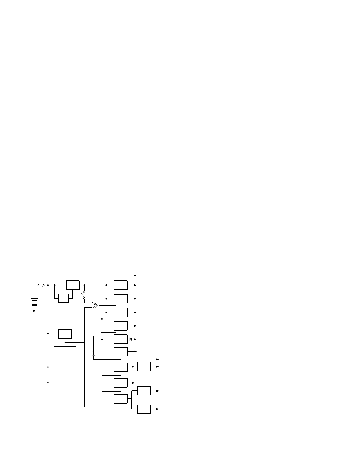
BLOCK DIAGRAM ................................................ 75
LEVEL DIAGRAM ................................................. 78
OPTIONAL ACCESSORIES
KNB-31A/32N/33L .......................................... 79
KSC-32 ............................................................. 79
SPECIFICATIONS .............................. BACK COVER
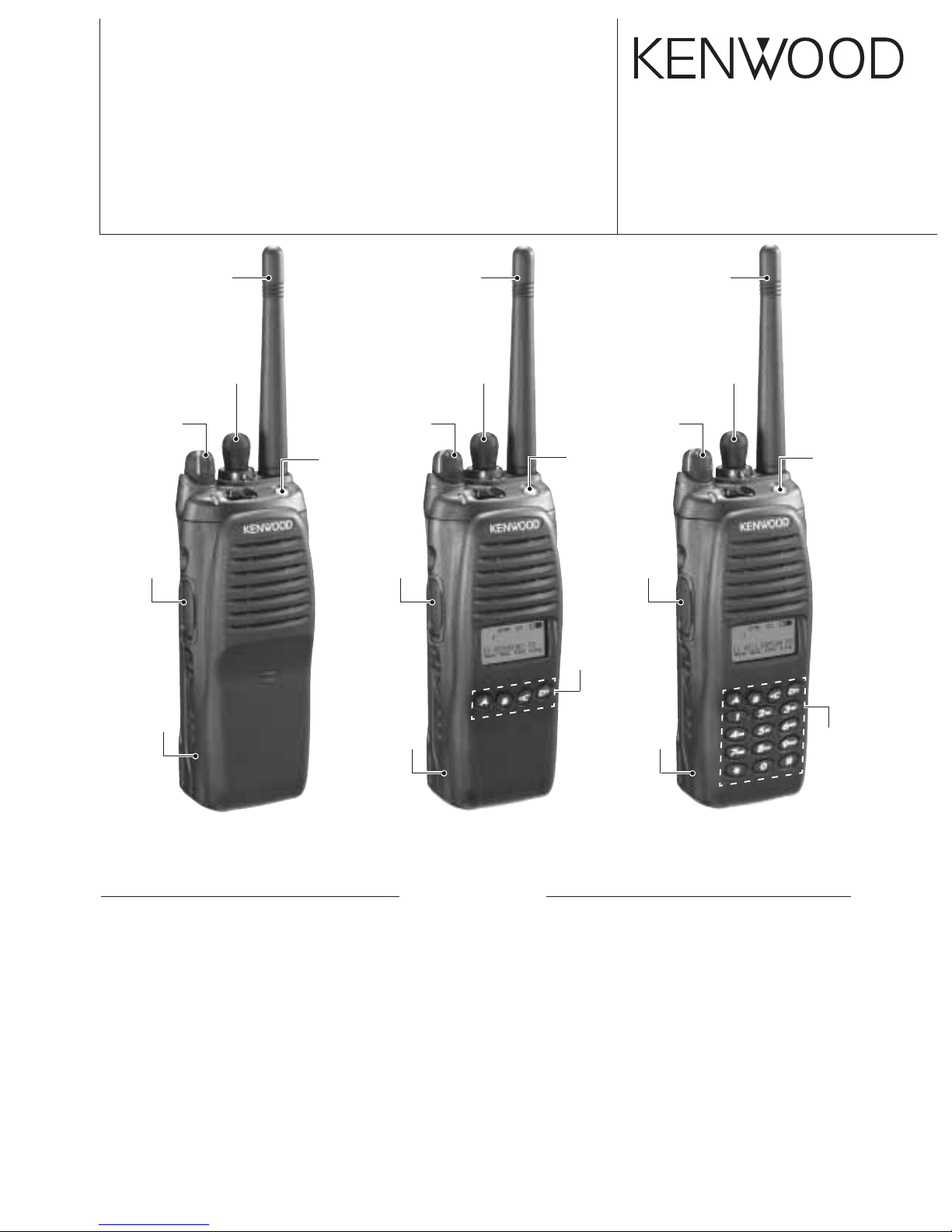
Helical Antenna
(KRA-22: Option)
Main cabinet
(A02-3875-01)
Knob (16CH)
(K29-9323-03)
Knob (Volume)
(K29-9322-03)
TK-5210 K TK-5210 K2 TK-5210 K3
CONTENTS
Knob (PTT)
(K29-9328-02)
Key top
(EMG)
(K29-9319-03)
Main cabinet
(4key)
(A02-3877-01)
Knob (16CH)
(K29-9323-03)
Knob (Volume)
(K29-9322-03)
Knob (PTT)
(K29-9328-02)
Key top
(EMG)
(K29-9319-03)
Main cabinet
(DTMF)
(A02-3879-01)
Knob (16CH)
(K29-9323-03)
Knob (Volume)
(K29-9322-03)
Knob (PTT)
(K29-9328-02)
Key top
(EMG)
(K29-9319-03)
Helical Antenna
(KRA-22: Option)
Helical Antenna
(KRA-22: Option)
Key top
(DTMF)
(K29-9321-13)
Key top
(4key)
(K29-9320-03)
TK-5210
2
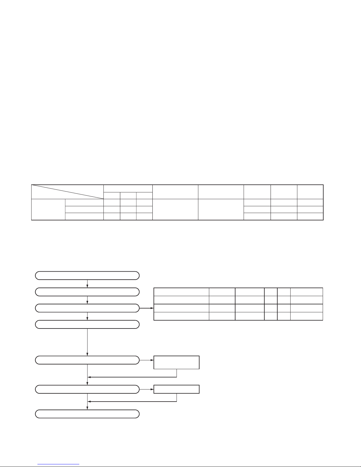
GENERAL / SYSTEM SET-UP
Model &
Unit X57-682X-XX
Frequency range Remarks LCD 4-key
DTMF
Destination (Market code)
0-10 0-11 0-12
keypad
K ✓
1st IF:49.95MHz
---
TK-5210 K2 ✓ 136~174 MHz
LOC:50.4MHz
✓✓
-
K3 ✓✓✓✓
INTRODUCTION
SCOPE OF THIS MANUAL
This manual is intended for use by experienced technicians familiar with similar types of commercial grade communications equipment. It contains all required service information for the equipment and is current as of the publication
date. Changes which may occur after publication are covered
by either Service Bulletins or Manual Revisions. These are
issued as required.
ORDERING REPLACEMENT PARTS
When ordering replacement parts or equipment information, the full part identification number should be included.
This applies to all parts : components, kits, or chassis. If the
part number is not known, include the chassis or kit number
of which it is a part, and a sufficient description of the required component for proper identification.
PERSONNEL SAFETY
The following precautions are recommended for person-
nel safety:
• DO NOT transmit until all RF connectors are verified secure and any open connectors are properly terminated.
•SHUT OFF and DO NOT operate this equipment near electrical blasting caps or in an explosive atmosphere.
• This equipment should be serviced by a qualified technician only.
SERVICE
This transceiver is designed for easy servicing. Refer to
the schematic diagrams, printed circuit board views, and
alignment procedures contained within.
SYSTEM SET-UP
Merchandise received
License and frequency allocated by FCC
Choose the type of transceiver
Transceiver programming
Are you using the optional antenna?
Are you using the speaker microphone?
A personal computer (IBM PC or compatible), programming
interface (KPG-36), and programming software (KPG-95D)
are required for programming.
(The frequency, and signaling data are programmed for the
transceiver.)
Frequency range (MHz) RF power Type LCD 4-key
DTMF keypad
TX/RX 136~174 5W TK-5120 K No No No
No
TX/RX 136~174 5W TK-5120 K2 Yes Yes
TX/RX 136~174 5W TK-5120 K3 Yes Yes Yes
YES
KRA-22 or KRA-26
Helical antenna
NO
NO
(Option)
(Option)
YES
KMC-25
Delivery
TK-5210
3
REALIGNMENT
1. Modes 2. How to Enter Each Mode
Mode Operation
User mode Power ON
Panel test mode ∗2 Press and hold the [Side3] and [PTT] keys
while turning the transceiver power on and
then release the [PTT] key first.
PC mode Received commands from PC
Panel tuning Press the [Side3] key, in Panel test mode
mode ∗2
Firmware
Press and hold the [Side3] and [PTT] keys
programming mode
while turning the transceiver power on and
then release the [Side3] key first.
Clone mode ∗2 Press and hold the [Side2] and [PTT] keys
while turning the transceiver power on and
then release the [Side2] key first.
Self
programming
Press and hold the [Side2] and [PTT] keys
mode ∗2 while turning the transceiver power on and
then release the [PTT] key first.
Firmware version
Press and hold the [Side3] key
information ∗2 while turning the transceiver power on.
Clock adjustment Press and hold the [Orange] and [PTT] keys
mode ∗2 while turning the transceiver power on and
then release the [Orange] key first.
3. Panel Test Mode (K2 and K3 models only)
Setting method refer to ADJUSTMENT.
4. Panel Tuning Mode (K2 and K3 models only)
Setting method refer to ADJUSTMENT.
User mode
Panel test mode
∗
1
Firmware version information
∗
1
Panel tuning mode ∗1
Data programming mode
PC test mode
PC tuning mode
PC mode
Clone mode ∗1
Firmware
programming mode
Clock adjustment mode ∗1
Self programming mode ∗1
Mode Function
User mode For normal use.
Panel test mode ∗1 Used by the dealer to check the fundamen-
tal characteristics.
Panel tuning mode ∗1
Used by the dealer to tune the transceiver.
PC mode Used for communication between the
transceiver and PC (IBM compatible).
Data programming Used to read and write frequency data and
mode other features to and from the transceiver.
PC test mode Used to check the transceiver using the PC.
This feature is included in the FPU.
See panel tuning.
Firmware Used when changing the main program of
programming mode the flash memory.
Clone mode ∗1 Used to transfer programming data from
one transceiver to another.
Self programming Frequency, signaling and features write to
mode ∗1 the transceiver.
Firmware version Used to confirm the internal firmware
information ∗1 version.
Clock adjustment Used by the dealer to adjust date and time.
mode ∗1
∗
1 : K2 and K3 models only
∗
2 : K2 and K3 models only
TK-5210
4
REALIGNMENT
5. PC Mode
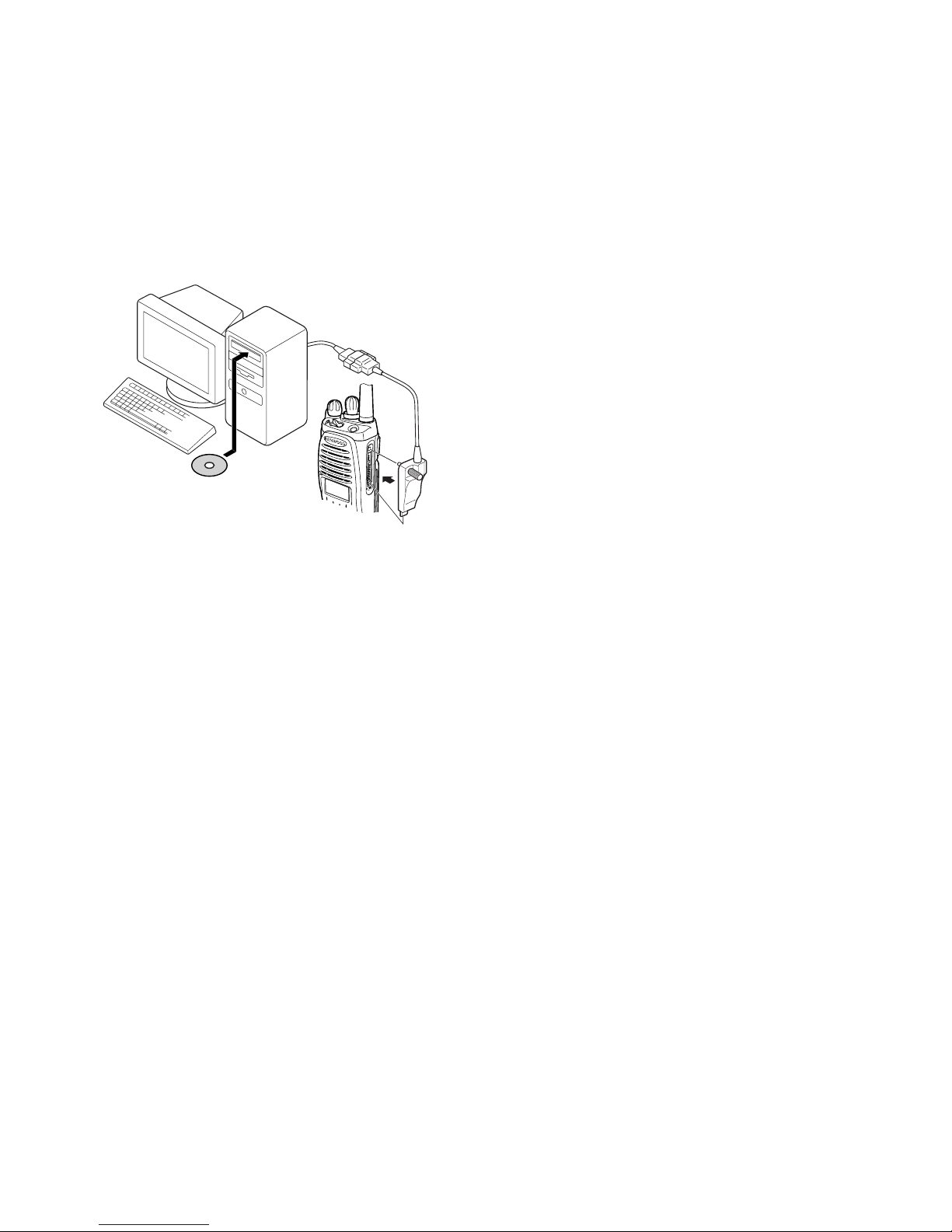
5-1. Preface
The transceiver is programmed by using a personal computer, programming interface (KPG-36) and programming
software (KPG-95D).
The programming software can be used with an IBM PC
or compatible. Figure 1 shows the setup of an IBM PC for
programming.
5-2. Connection procedure
1. Connect the transceiver to the personal computer with
the interface cable.
2. When the POWER switch on, user mode can be entered
immediately. When PC sends command the transceiver
enter PC mode, and “PROGRAM” is displayed on the
LCD.
When data transmitting from transceiver, the red LED is
lights.
When data receiving to transceiver, the green LED is
lights.
Notes:
• The text message are displayed for K2 and K3 models
only.
• The data stored in the personal computer must match
"Model Name and Market Code", when it is written into
the EEPROM and flash memory.
5-3. KPG-36 description
(PC programming interface cable: Option)
The KPG-36 is required to interface the transceiver to the
computer. It has a circuit in its D-sub connector (25-pin) case
that converts the RS-232C logic level to the TTL level.
The KPG-36 connects the universal connector of the transceiver to the computers RS-232C serial port.
5-4. Programming software KPG-95D description
The KPG-95D is the programming software for the transceiver supplied on a CD-ROM. This software runs under MSWindows 98, ME, Windows 2000 or XP on an IBM-PC or
compatible machine.
The data can be input to or read from the transceiver and
edited on the screen. The programmed or edited data can be
printed out. It is also possible to tune the transceiver.
6. Firmware Programming Mode
6-1. Preface
Flash memory is mounted on the transceiver. This allows
the transceiver to be upgraded when new features are released in the future. (For details on how to obtain the firmware, contact Customer Service.)
6-2. Connection procedure
Connect the transceiver to the personal computer (IBM
PC or compatible) with the interface cable (KPG-36). (Connection is the same as in the PC Mode.)
6-3. Programming
1. Start up the firmware programming software (Fpro.exe).
2. Set the communications speed (normally, 115200 bps)
and communications port in the configuration item.
3. Set the firmware to be updated by File name item.
4. Press and hold the [Side3] and [PTT] keys while turning
the transceiver power on and then release the [Side3] key
first. Then, the orange LED on the transceiver lights and
the baud rate is displayed as follows according to the posi-
tion of the Concentric switch.
A: PROGRAM 115200 bps
B: PROGRAM 57600 bps
C: PROGRAM 19200 bps
Since the baud rate is normally set to 115200 bps, change
the Concentric switch to "A".
5. Check the connection between the transceiver and the
personal computer, and make sure that the transceiver is
in the Program mode.
6. Press “write” button in the window. When the transceiver starts to receive data, the [PG] display lights.
7. If writing ends successfully, the checksum is calculated
and a result is displayed.
8. If you want to continue programming other transceivers,
repeat steps 4 to 7.
Notes:
• This mode cannot be entered if the Firmware Programming mode is set to Disable in the Programming software.
• The text message are displayed for K2 and K3 models
only.
6-4. Baud rate change
1. Change baud rate by changing the Concentric switch position. The baud rates are assigned to positions of the Concentric switch as follows:
A: PROGRAM 115200 bps
B: PROGRAM 57600 bps
C: PROGRAM 19200 bps
2. If you press the [Side1] switch (top of left side) while the
baud rate (such as “PROGRAM 115200 bps") is displayed,
the checksum is calculated, and a result is displayed. If
you press the [Side1] switch again while the checksum is
displayed, the baud rate (such as “PROGRAM 115200
bps") is redisplayed.
Notes:
• Normally, write in the high-speed mode.
• The text message are displayed for K2 and K3 models
only.
Fig. 1
IBM-PC
KPG-36
KPG-95D
TK-5210
5
REALIGNMENT
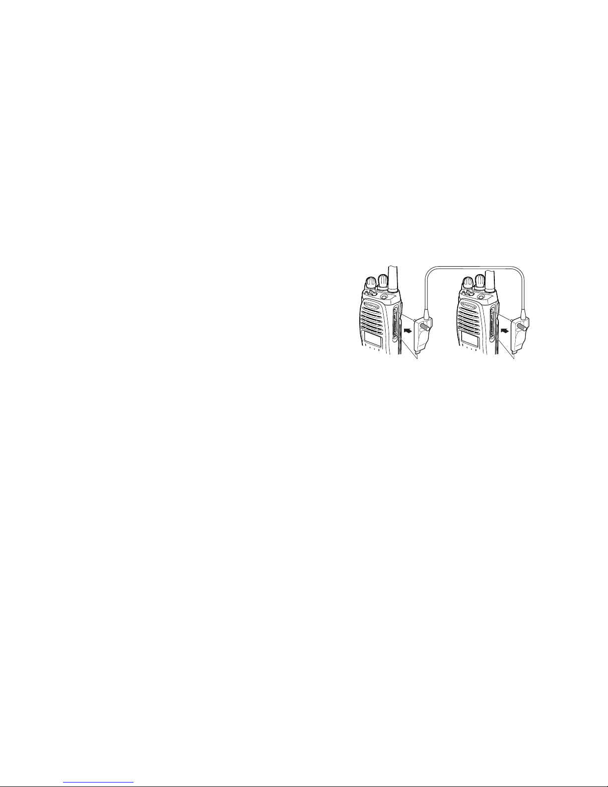
7. Clone Mode (K2 and K3 models only)
Programming data can be transferred from one transceiver to another by connecting them via their external universal connectors. The operation is as follows (the transmit
transceiver is the master and the receive transceiver is a
slave).
The following data cannot be cloned.
• Tuning data
• Embedded message with password
• Model name data
• ESN data
Key guide on the "INPUT PASSWORD" display.
• CNF([A] key): The password confirmation
• DEL([B] key): Delete the least digit from the current pass-
word number
• SET([D] key): Determine the least digit of the password
number
1. Press and hold the [Side2] and [PTT] keys while turning
the transceiver power on and then release the [Side2] key
first. If the Read authorization password is set to the trans-
ceiver, the transceiver displays “CLONE LOCK”. If the
password is not set, the transceiver displays “CLONE
MODE”.
2. When you enter the correct password, and “CLONE
MODE” is displayed, the transceiver can be used as the
cloning master. The following describes how to enter the
password.
3.
• How to enter the password using the keypad (K3 model
only);
If the [D] key is pressed while "CLONE LOCK" is displayed,
the Read authorization password input screen (INPUT
PASSWORD) is displayd.
If one of keys 0 to 9 is pressed while "INPUT PASSWORD"
is displayed, the pressed number is displayed on the LCD.
Each press of the key shifts the display in order to the left.
When you enter the password and press the [A] or [✳]
key, “CLONE MODE” is displayed if the entered pass-
word is correct. If the password is incorrect, “CLONE
LOCK” is redisplayed.
• How to enter the password using the [Side2] and [Side3]
keys (K2 and K3 models);
If the [D] key is pressed while "CLONE LOCK" is displayed,
the Read authorization password input screen (INPUT
PASSWORD) is displayd.
If the [Side2] key or [Side3] key is pressed while "INPUT
PASSWORD" is displayed, the number (0 to 9) flashes on
the LCD. When you press the [D] key, the currently
selected number is determined. If you press the [A] key
after entering the password in this procedure, “CLONE
MODE” is displayed if the entered password is correct. If
the password is incorrect, “CLONE LOCK” is redisplayed.
4. Power on the slave transceiver.
5. Connect the cloning cable (part No. E30-3325-05) to the
universal connectors on the master and slave.
6. Press the [Side1] or [A] key on the master while the mas-
ter displays “CLONE MODE”. The data of the master is
sent to the slave. While the slave is receiving the data,
“PROGRAM” is displayed. When cloning of data is com-
pleted, the master displays “END”, and the slave automatically operates in the User mode. The slave can then
be operated by the same program as the master.
7. The other slave can be continuously cloned. When the
[Side1] or [A] key on the master is pressed while the master displays “END”, the master displays “CLONE
MODE”. Carry out the operation in step 4 to 6.
Notes:
• Can not be cloned if the password (over write password)
is programmed to the slave.
•"Model Name and Market Code" must be same to clone
the transceiver. However, it may be unable to clone the
transceiver depending on the enhanced features settings.
(Refer to the FPU for the enhanced features details.)
8. Self Programming Mode
(K2 and K3 models only)
Write mode for frequency data and signaling etc. To be
used ONLY by the authorized service person maintaining the
user's equipment. After programming, reset the FPU to the
"Self- Programming" disabled mode. Transceivers CANNOT
be delivered to the end-user in the self-programming mode.
The following setup items in the channels programmed by
the FPU can be changed using the self-programming mode.
The addition of new channel and the deletion of channel that
has already been programmed by the FPU cannot be
performed using the self-programming mode.
• RX frequency
• TX frequency
• Channel type
• TX mode (When the channel type is selected "MIXED".)
• Channel spacing
• RX signaling
• TX signaling
• RX NAC
• TX NAC
• Talkgroup list number
Note:
The personality will be also changed when the abovementioned items is changed. (Refer to the FPU for the
personality details.)
Key guide on the "INPUT PASSWORD" display.
• CNF([A] key): The password confirmation
• DEL([B] key): Delete the least digit from the current pass-
word number
Cloning cable
(E30-3325-05)
Fig. 2
TK-5210
6
REALIGNMENT
No. Setup item Display Remarks
1 Select ZONE [**] -CH *** Zone : 1~50
Zone/Channel ZONE ** -CH [***] CH : 1~250
2 RX frequency RX Freq Receive frequency
3 TX frequency TX Freq Transmit frequency
4 Channel type CH Type ANALOG/APCO/MIXED
5 TX mode TX Mode ANALOG/APCO
6Channel spacing CH Space 25.0kHz/12.5kHz
(When the Channel type is selected "ANALOG" or "MIXED".)
APCO 12.5kHz/12.5kHz (When the Channel type is selected "APCO".)
7 RX Signaling RX Sig Receive QT/DQT
8 TX Signaling TX Sig Transmit QT/DQT
9 RX NAC RX NAC *** 000~FFF (Hexadecimal)
10 TX NAC TX NAC *** 000~FFF (Hexadecimal)
11 Talkgroup list number TG List No. *** 1~250
The setup items for self programming mode are as follows.
Item
Zone-Channel RX Frequency TX Frequency Channel Type TX Mode Channel Spacing RX Signaling TX Signaling
Key
[A] Go to the next item
Zone/ Channel
2.5kHz/5kHz/6.25kHz/
QT/DQT(N)/DQT(I)/OFF
[B]
switching
7.5kHz/1MHz Unused
switching
step switching
[C]
Zone/ Channel
1 step down
ANALOG/APCO/MIXED
ANALOG/APCO Channel spacing
Signaling down
down switching(Back) switching(Back) switching(Back)
[D]
Zone/ Channel
1 step up
ANALOG/APCO/MIXED
ANALOG/APCO Channel spacing
Signaling up
up
switching(Forward) switching(Forward) switching(Forward)
[Side3]
Data
Unused
ON/OFF
Unused
1 step/Standard
writing switching switching
Key operation
Item
RX NAC TX NAC TG List No.
Key
[A] Go to the next item
[B]
Delete the least digit from the current number
Unused
(Press and hold to delete all numbers.)
[C] Unused
TG List
number down
[D] Determine the least digit
TG List
number up
[Side2] Increment a number in the specified digit Unused
[Side3] Decrement a number in the specified digit Unused
Keypad Add a digit to the
Unused
(K3 model only)
current number
• SET([D] key): Determine the least digit of the password
number
8-1. Enter to the self programming mode
Press and hold the [Side2] and [PTT] keys while turning
the transceiver power on and then release the [PTT] key first.
Ignoring whether the Read authorization password is set or
not, "INPUT PASSWORD" appears.
If the Read authorization password is not set to the transceiver, "SELF PROG MODE" is displayed on the LCD when
the [A] key is pressed while "INPUT PASSWORD" is displayed.
If the password is set to the transceiver, "SELF PROG
MODE" is displayed on the LCD when you enter the correct
password while "INPUT PASSWORD" is displayed.
For the password input method, see "7.Clone Mode”
step 3 described on page 5.
Note :
This mode (self programming mode) cannot be set when
it has been disabled with the FPU.
8-2. Data Writing
If the [Side3] key is pressed while Zone/Channel mode is
displayd, new data is written into memory. "Writing" is displayed while the transceiver is writing data.
TK-5210
7
REALIGNMENT
●
Self programming mode flow chart
9. Firmware Information Mode
(K2 and K3 models only)
Turn the transceiver ON with the [Side3] key held down.
Then, the version is displayed during holding the [Side3] key.
10.Clock Adjustment Mode
(K2 and K3 models only)
10-1. Flow chart of operation
[Orange] + [PTT] + Power ON Release [Orange]
MINUTE
HOUR
DAY
MONTH
YEAR
[A]
[A]
[A]
[A]
[A]
[Side2] and [Side3] keys or [C] and [D] keys
[Side2] and [Side3] keys or [C] and [D] keys
[Side2] and [Side3] keys or [C] and [D] keys
[Side2] and [Side3] keys or [C] and [D] keys
[Side2] and [Side3] keys or [C] and [D] keys
Completion
TX NAC
[A]
RX NAC
[A]
TX signaling
[A]
[A]
RX signaling
[A]
[A] [A]
[A]
*1
*2
[A]
TX frequency
RX frequency
[A] When the [Side3] key is pressed, new data is written into memory.
[A]
Zone/Channel
[A]
Read authorization password entry (6 digits)
[A]
[Side2] + [PTT] + POWER ON Release [PTT]
[TX frequency] : Other than "OFF"
[Channel type] : "MIXED"
[TX frequency] : Other than "OFF"
[Channel type] : "ANALOG" or "MIXED"
[TX mode] : "ANALOG"
[TX frequency] : "OFF"
[TX frequency] : Other than "OFF"
[Channel type] : "APCO" or "MIXED"
If [Channel type] is set to "MIXED", [TX mode] must be set to "APCO".
[Channel type] : "ANALOG" or "MIXED"
[A]
[Channel type] : "APCO"
[TX frequency] : "OFF"
[Channel type] : "ANALOG" or "APCO"
[TX frequency] : "OFF"
[Channel type] : "APCO" or "MIXED"
[A]
[TX frequency] : "OFF"
[Channel type] : "ANALOG"
[A]
[Channel type] : "ANALOG"
[A]
Talkgroup ID List Amount : 0
[Channel type] : "APCO" or "MIXED"
[Channel type] : "APCO" or "MIXED"
Talkgroup ID List Amount must not be 0.
Self programming mode
Input Password
OFF QT
OFF
Zone selection
APCO
Channel selection
Talkgroup list number
[A]
[A]
[A]
[Side 3]
[B]
DQT N
[B]
[B]
DQT I
[B]
[B] [B] [B]
[B]
ANALOG
Channel type
[C]/[D]
APCOANALOG
TX mode
[C]/[D]
Channel spacing
12.5kHz25.0kHz
[C]/[D]
12.5kHz
*1 [Channel type] : "ANALOG" or "MIXED"
*2 [Channel type] : "APCO"
APCO 12.5kHz
[C]/[D]
[C]/[D]
MIXED
[C]/[D]
OFF QT DQT N
[B]
DQT I
TK-5210
8
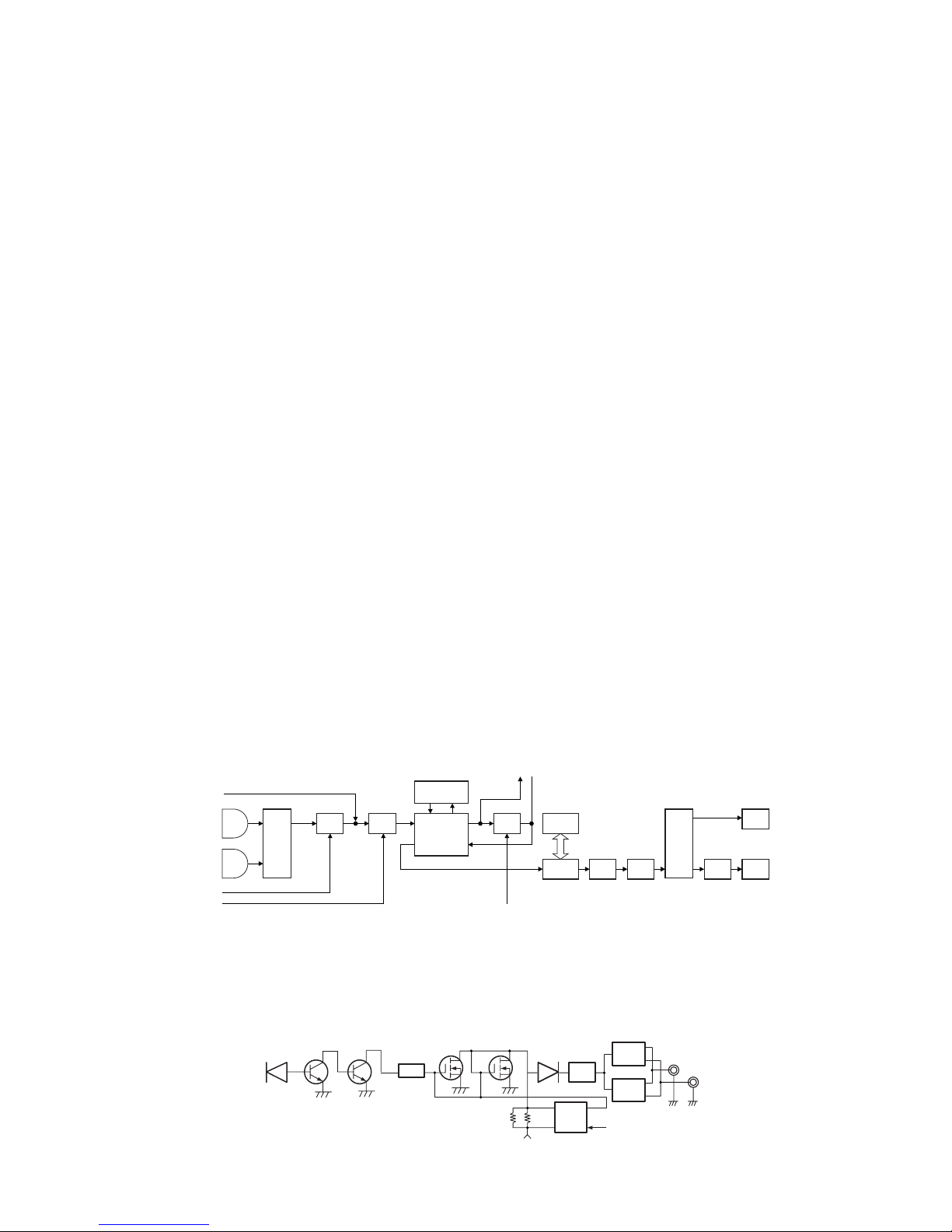
DISASSEMBLY FOR REPAIR
Disassembly Procedure
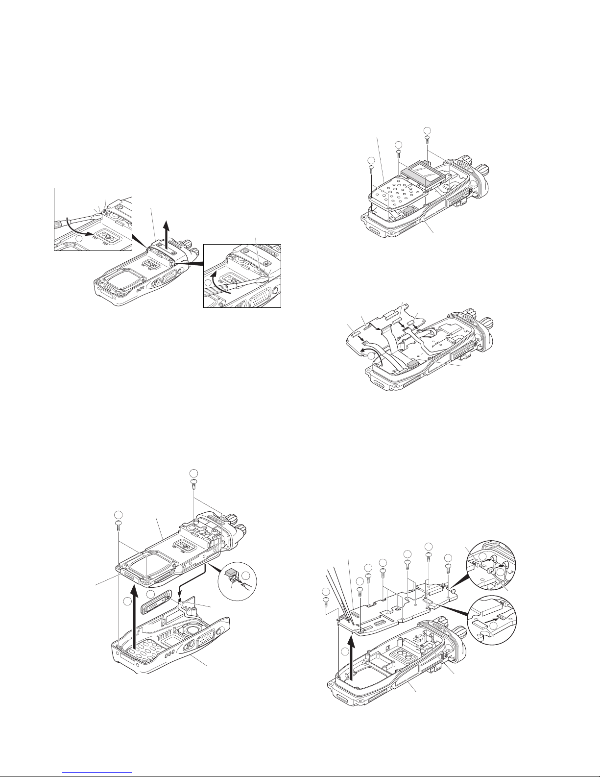
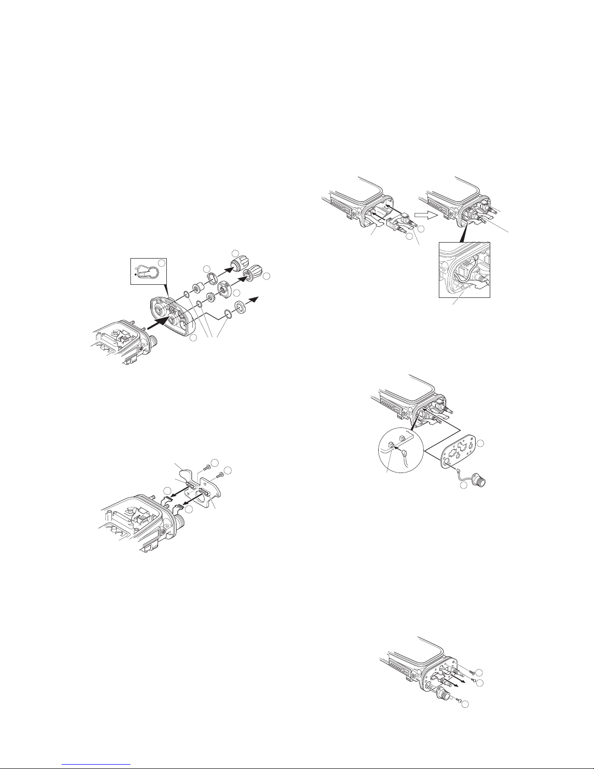
■ Removing the front case from the chassis.
1. Remove the rear panel with a flat-head screwdriver.
Insert the screwdriver between the rear panel (right side)
and the chassis (the place next to the """ mark shown on
the chassis), push it in the direction of the arrow
1, and
remove the right side of the rear panel. Repeat the above
action for the left side of the rear panel 2.
2. Remove the four screws 3 and universal connector cap
4.
3. Lift the battery pack release latch on the bottom of the
chassis
5 and remove the chassis from the front case.
Notes:
• Lift the chassis from the front case slowly and carefully. If
the chassis is lifted suddenly, the SP/MIC FPC may be
pulled and the connector may become damaged.
• Handle the main packing with care. It is likely to collect
dust and dirt.
4. Remove the SP/MIC FPC from the CONTROL PCB connector (CN603).
6
■ Removing the CONTROL PCB (X57-682 B/5)
from the chassis.
1. Remove the six screws 7.
2. On the reverse side of the CONTROL PCB
8, remove the
cord ASSY and each FPC from the connectors (CN601,
CN604 (K2 and K3 models only), CN752, CN753) of the
CONTROL PCB.
■ Removing the TX-RX PCB (X57-682 A/5) from
the chassis.
1. Remove the 14 screws 9.
2. Remove the universal connector FPC from the TX-RX PCB
connector (CN7) 0.
3. Insert the two tips of a pair of tweezers into the two holes
in the bottom of the shield plate of the TX-RX PCB, firmly
squeeze the tweezers to hold the shield plate, then
remove the TX-RX PCB
!.
4. Remove the coaxial cables from the two connectors
(MAIN (CN101), UNIV (CN102)) of the TX-RX PCB @.
1
2
Rear panel
""" mark
""" mark
3
3
5
4
6
CN603
Chassis
Battery pack
release latch
SP/MIC FPC
Front case
7
7
7
CONTROL PCB
Chassis
CN604
CN601
CN752
CN753
8
Cord ASSY
CN7
UNIV
(CN102)
MAIN
(CN101)
9
11
10
9
9
9
9
9
9
12
12
TX-RX PCB
Chassis
Universal
connector FPC
TK-5210
9
DISASSEMBLY FOR REPAIR
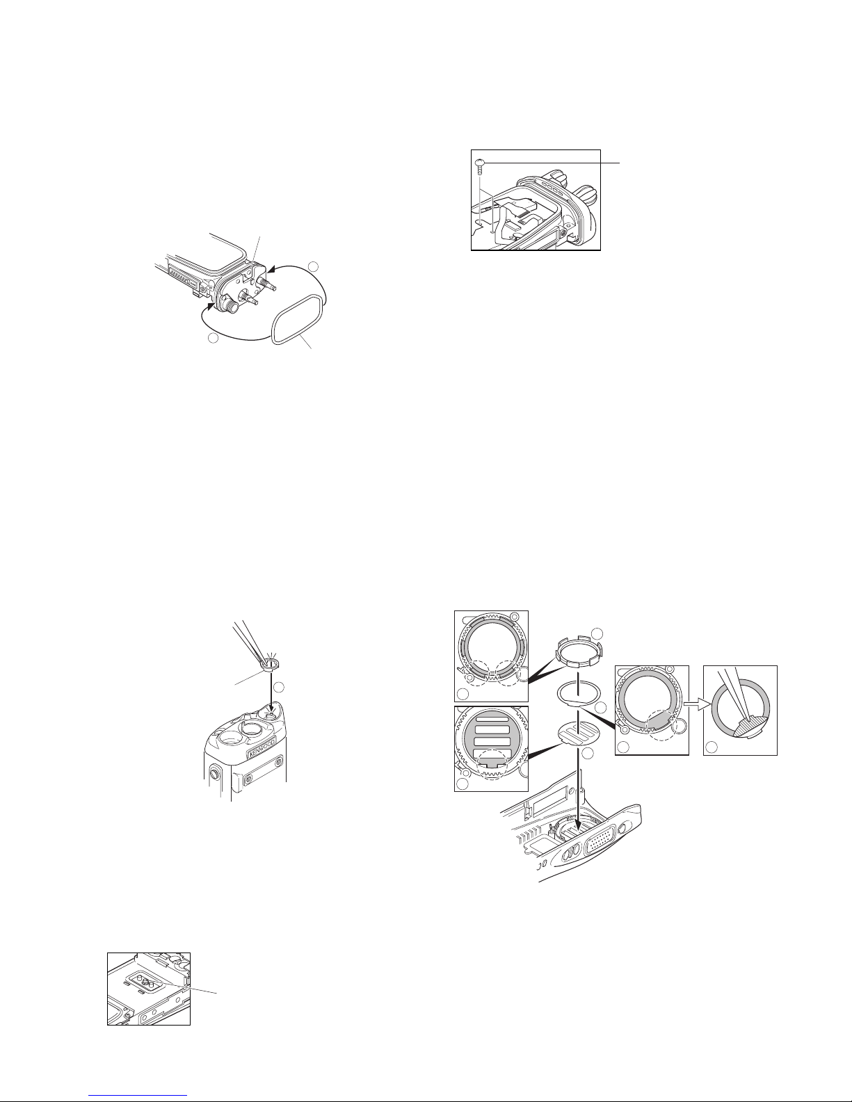
■ Removing the top panel from the chassis.
1. Remove the volume knob # and channel knob $.
2. Remove the concentric switch knob
%.
3. Remove the volume torque-up packing
^ using a pair of
tweezers.
4. Remove the nuts from the volume knob, channel knob
and antenna receptacle.
5. Remove the top panel
&.
Notes:
•Before removing the top panel, set the lever switch to the
"-" position (circle painted in white)
*.
• Each of the volume knob, channel knob and antenna receptacle on the top panel has an O-ring. Take care not to
lose them after removing the panel.
■ Removing the TOP PCB (X57-682 C/5) from the
chassis.
1. Remove the two screws (.
2. Lift the TOP PCB and remove the VOL/CH FPC
) and
CONTROL-TOP FPC
⁄ from the two connectors (CN902,
CN903) of the TOP PCB.
Precautions for Reassembly
■ Installing the VOL/CH FPC and CONTROL-TOP
FPC on the TOP PCB
1. Remove the volume 1 and channel switch 2 from the
chassis.
2. Position the coaxial cable connecting the ANT PCB and
TX-RX PCB as shown in the figure below.
3. Pass the coaxial cable
3 of the antenna receptacle
through the round hole of the hardware fixture
4, then
insert it into the coaxial connector (MAIN (CN101)) of the
TX-RX PCB.
4. Pass the volume, channel switch, VOL/CH FPC and
CONTROL-TOP FPC through hardware fixture holes, then
bring the hardware fixture into contact with the chassis
and fix it with a screw
5.
Note:
The projections of the volume and channel switch pedestals must protrude from the square holes of the hardware
fixture.
5. Fix the antenna receptacle with the two screws 6.
6. Fix the hardware fixture with a screw
7.
13
14
15
17
16
18
O-ring
CN902
TOP PCB
CN903
19
19
20
21
1
2
CONTROL-TOP
FPC
VOL/CH FPC
The projection
of the volume
pedestal
The projection of
the channel
switch pedestal
Aline the coaxial cable
connecting the ANT PCB and
TX-RX PCB as shown in the figure.
4
3
MAIN
(CN101)
5
7
6
TK-5210
10
DISASSEMBLY FOR REPAIR
7. Insert the VOL/CH FPC 8 and the CONTROL-TOP FPC 9
into the connectors (CN902, CN903) of the TOP PCB.
8. Fix the TOP PCB with a screw
0.
9. Fix the TOP PCB with a screw
!.
■ TX-RX PCB Installation Procedure
1. Insert the coaxial cable of the antenna receptacle into the
coaxial connector (CN101) of the TX-RX PCB
1 and the
coaxial cable of the ANT PCB into the coaxial connector
(CN102) of the TX-RX PCB
2.
2. Grasp both sides of the lower part of the TX-RX PCB, tilt
the TX-RX PCB and install the chassis so that the PTT FPC
3, CONTROL-TOP FPC 4 and universal connector FPC
5 are not caught 6.
3. Fix the TX-RX PCB with the 14 screws.
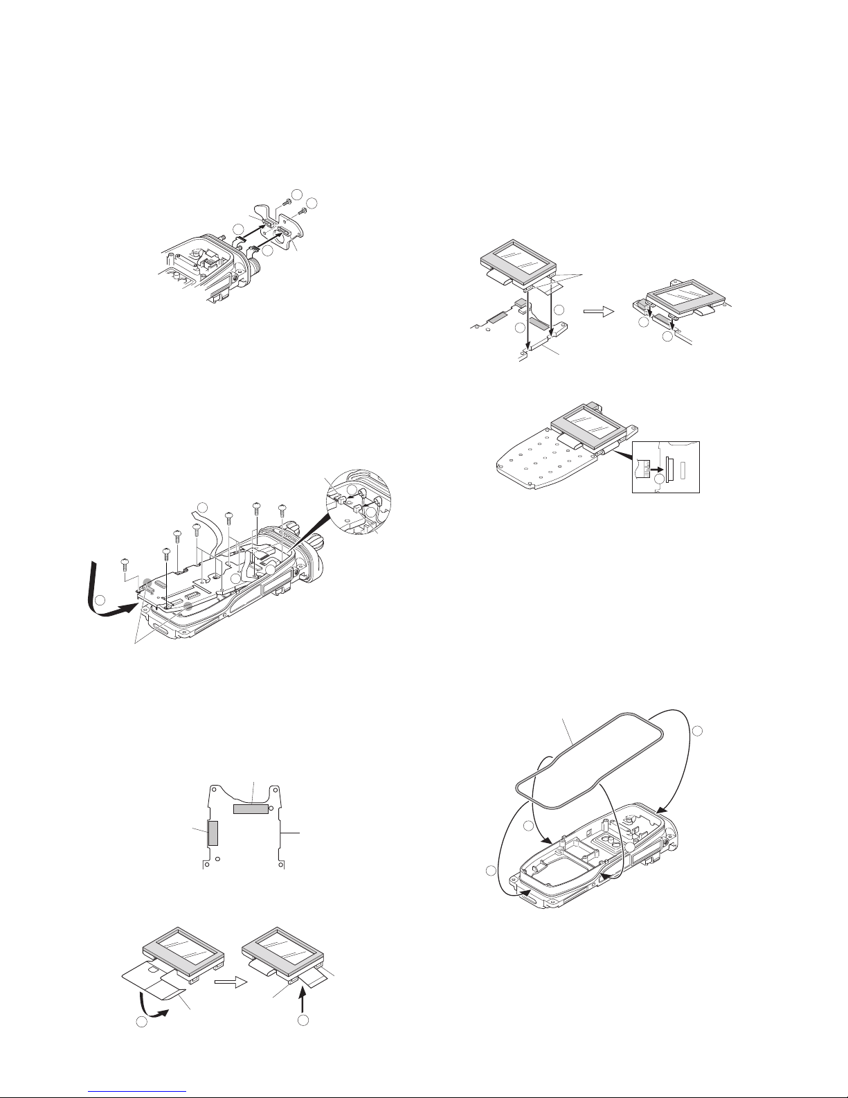
■ LCD ASSY Installation Procedure (K2 and K3
models only)
1. Remove the two adhesive sheets attached to the
CONTROL PCB, and attach the new adhesive sheets to
the location as shown in the following figure.
2. Fold the LCD ASSY FPC to the back of the holder
1 so
that the FPC is between the two tabs on the right side of
the holder
2.
3. Fit the two tabs on the right side of the holder 3 and the
two tabs on the left side of the holder
4 into the
CONTROL PCB.
Note:
Take care that the FPC is not caught when fitting the two
tabs on the right side of the holder.
4. Insert the FPC into the CONTROL PCB connector (CN751)
5.
■
Main Packing (G53-1637-04) Installation Procedure
1. Hook the packing (coated with silicon oil) in the upper
groove of the chassis
1, then fit the packing into the
lower groove of the chassis
2.
Note:
Ensure that the chassis grooves and packing are free from
dirt and dust.
2. Fit the packing into the grooves on both sides of the
chassis 3. (Fit the packing into the groove in the chassis
by tracing it lightly with your fingers.)
Note:
To remove the packing from the chassis groove, use a
resin adjustment bar or other such device. If the packing
is pried with a sharp metallic tool, such as tweezers, the
packing may become damaged.
3. Verify that the packing fits snuggly into the groove of the
chassis.
CN902
CN903
10
11
8
9
CN102
CN101
3
1
2
4
6
5
Grasp both sides of the lower part
of the TX-RX PCB
2
1
LCD ASSY FPC
tab
tab
CN751
5
1
2
3
3
Main packing
4
4
3
3
tab
CONTROL PCB
Adhesive sheet
(J99-0394-04)
Adhesive sheet
(J99-0393-04)
CONTROL PCB
TK-5210
11
2. Tighten the two screws from the TX-RX PCB side.
3. Firmly tighten the hexagon screws of the GND terminal.
Installation Procedure during Parts
Replacement
■ Attaching the Sheet (G10-1338-04, J99-0383-14)
to the Front Case Speaker and Installation of
the Packing (G53-1633-04)
1. Attach a new fiber sheet 1 (G10-1338-04) so that its
convex fits the hollow of the front case
2.
2. Attach a new pressure sensitive adhesive sheet
3 (J99-
0383-14) so that its convex fits the hollow of the front
case 4.
3. Remove the separation sheet from the pressure sensitive
adhesive sheet with a pair of tweezers 5.
4. Fit the packing
6 (G53-1633-04) into the front case
speaker.
Note:
Fit the packing into the hollow of the case so that the two
low-height places in the convex of the packing are positioned on the lower side
7.
5. Verify that the packing does not ride on the rib of the case.
DISASSEMBLY FOR REPAIR
■ Top Packing (G53-1638-04) Installation Procedure
1. Ensure that the hardware fixture is first secured to the
chassis.
2. Hook the packing (coated with silicon oil) in the upper left
groove of the chassis
1, then fit the packing into the right
groove of the chassis.
2
Notes:
• Verify that the chassis grooves and packing are free from
dirt and dust.
• To remove the packing from the chassis groove, use a
resin adjustment bar or other such device. If the packing
is pried with a sharp metallic tool, such as tweezers, the
packing may become damaged.
3. Verify that the packing fits snuggly into the groove of the
chassis.
■ Volume Torque-up Packing (G53-1628-04)
Installation Procedure
Insert the packing using a pair of tweezers so that the
hollow of the packing fits the convex of the panel
1.
■ Screw sequence for mounting the battery
terminal block to the chassis.
Attach the battery terminal block to the chassis as
described in the following procedure.
1. Loosely fix the hexagon screws of the GND terminal to
the chassis (enough so that the hexagon screws do not
move).
2
1
Top packing
Hardware fixture
1
Volume torque-up packing
GND terminal
Two screws
2
4 5
3
6
1
7
TK-5210
12
■ Installing a new LCD ASSY to the holder (K2
and K3 models only)
1. Remove the separation paper (brown) from the new sheet
1 2, and attach the sheet to the surface of the holder 3.
2. Remove the protection sheets attached to both sides of
the new LCD ASSY.
3. Remove the separation paper (white) from the sheet in
step 1
4, then attach the LCD ASSY 5 to the sheet.
4. Attach two pieces of double-sided adhesive tape
6 to the
back of the holder and remove the separation paper.
5. Remove the protection sheet (transparent) attached to
one side of the new filter
7 8 and remove the protection
sheet (yellow) from the other side
9.
6. Attach the filter from step 5 to the back of the holder.
7. Attach the new cushion 0 so that it fits to the corner of
the holder convex.
■ Preparation when Replacing the Cord ASSY
(X42-3270-10)
Cut the tip of the FPC on the side on which "TX-RX" is
stamped when replacing the cord ASSY.
2
1
1
3
3
7
6
6
5
10
5
4
6
8
9
6
10
CUT
TX-RX
CONT
Cord Assy(X42-3270-10)
■ Procedures when Replacing the Top Panel
1. Insert the O-ring 1 into the lever switch part of the new
top panel.
2. Apply grease to the base of the shaft of the lever knob 2
and install the lever knob so that it is in the "-" position
(circle painted in white) on the top panel
3.
3. Pass the hardware fixture
4 through the shaft and install
it onto the top panel.
4. Apply grease to between the two holes in the hardware
fixture
4.
5. Install the hardware fixture
5 so that it is inserted into the
hole on the left side of the hardware fixture
4.
6. Fix the two hardware fixtures with the hexagon nut
6.
7. Apply bond (Three Bond 1401C) to the tip of the lever
knob shaft and the surface of the hexagon nut
7.
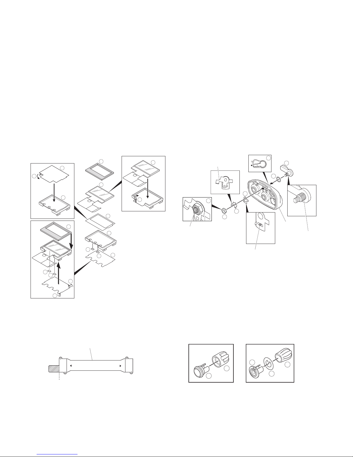
■ Volume Knob and Channel Knob Parts Replace-
ment
Since the volume knob consists of two components, a
knob
1 and a spacer 2, replace and reinstall these two
parts at the same time.
Since the channel knob consists of three components, a
knob
3, a 16CH display seal 4 and a spacer 5, replace
and reinstall these three parts at the same time.
1
3
2
4
5
6
7
Apply grease to between
the two holes in
the hardware fixture.
Apply bond (Three Bond 1401C)
to the tip of the lever knob shaft
and the surface of the hexagon
nut.
Top panel
Inserted into the hole
on the left side of the
hardware fixture.
Apply grease to the
base of the shaft of
the lever knob.
1
3
4
5
2
Volume Knob Channel Knob
DISASSEMBLY FOR REPAIR
TK-5210
13
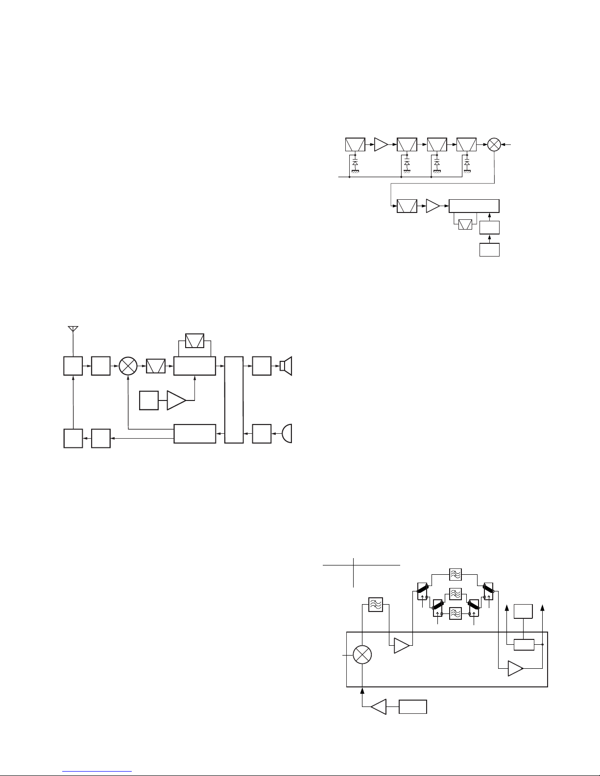
CIRCUIT DESCRIPTION
1. Overview
This transceiver is a VHF/FM/APCO portable transceiver
designed to operate in the frequency range of 136 to
174MHz.
The unit consists of receiver, transmitter, phase-locked
loop (PLL) frequency synthesizer, base band parts, power
supply, and control circuits.
2. Frequency Configuration
The receiver is a double-conversion superheterodyne
using first intermediate frequency (IF) of 49.95MHz and
second IF of 450kHz. Incoming signals from the antenna are
mixed with the local signal from the PLL circuit to produce
the first IF of 49.95MHz.
This is then mixed with the 50.4MHz second local
oscillator output to produce the 450kHz second IF. This
signal is detected to give the demodulated signal in the DSP.
The transmit signal frequency is generated by the PLL
VCO, and modulated by the signal from the DSP. It is then
amplified and fed to the antenna.
3. Receiver System
3-1. Front-end RF Amplifier
The signal is passed through an antenna matching coil,
where the high-frequency components are amplified by a
GaAs FET(Q202). The signals are then fed into band-pass
filter that uses varactor diode tuning to reject unwanted
signal components, and is fed to the 1st mixer.
3-2. 1st Mixer
The 1st mixer uses the GaAs IC (IC202). The 1st mixer
mixes the signal with the 1st local oscillator frequency from
the VCO, and converts it to the 1st IF (49.95MHz).
The signal then passes through monolithic crystal filter
(XF201) to remove unnecessary nearby frequency
components. The signal from the MCF is used as the 1st IF
signal.
3-3. IF Amplifier
The 1st IF signal is amplified by the IF amplifier (Q204) and
fed into the FM IC (IC204). The IF signal is then mixed with
the 2nd local oscillator frequency of 50.4MHz to generate the
Fig. 1 Frequency configuration
ANT
TX/RX : 136~174MHz
ANT
SW
RF
AMP
PA
AMP
TX
AMP
1st MIX
MCF
VCXO
49.95MHz
CF
450kHz
MIX
IF AMP
AF
AMP
SP
16.8MHz
50.4MHz
x3
185.95~
223.95MHz
136~174MHz
PLL
VCO
FPGA
A/D
D/A
DSP
MIC
AMP
MIC
2nd IF of 450KHz. The 450KHz signal is then passed through
a ceramic filter (CF201) and fed back into IC204 for additional
amplification.
3-4. Wide/ Narrow/ APCO Switching Circuit
Narrow and Wide and APCO settings can be made for
each channel by switching the ceramic filters CF203 (Wide),
CF204 (Narrow), CF202 (APCO).
The Wide and Narrow and APCO data is output from pin54
(WN) and pin55 (VN) of CPU (IC5).
When a Wide data (VN : low level, WN : high level) is
received, the 450KHz signal is passed through a ceramic filter
(CF203). When a Narrow data (VN : low level, WN : low level)
is received, the 450KHz signal is passed through a ceramic
filter (CF204). When a APCO data (VN : high level, WN : high
level) is received, the 450KHz signal is passed through a
ceramic filter (CF202).
If the 450kHz signal is a FM signal(Wide, Narrow), the
signal is detected by a ceramic discriminator (CD201). AF
signal is fed to CODEC(IC406), the AF level is adjusted and it
is output from 15pin of IC406. Q209 turns on/off with the
Wide/Narrow data and the IC204 detector output level is
changed to maintain a constant output level during Wide or
Narrow signals.
If the 450kHz signal is an APCO signal, the signal is
prepared by the buffer amplifier (IC208) and fed to FPGA
(IC13). The APCO signal is A/D-converted by the FPGA and
DSP (IC8), and is performed APCO demodulation.
The AF signal is output from 15pin of CODEC (IC406).
1st Local OSC
BPF BPF BPF
1st
LNA MIXER
Q202L201
TUNE
L204 L205 IC202
MCF
XF201
49.95MHz
IF AMP
Q204
Q205
2nd Local OSC
FM IC
IC204
Tripler
X3
CF201
BPF
L202
X201
16.8MHz
VCXO
WN WN
VNVN
CF203
CF204
CF202
APCO
Narrow
Wide
IC203
IC205
IC206
IC207
CF201
16.8MHz
VCXO
X201
x3
Q205
50.4MHz
49.95MHz
450kHz
IC204
FM IC
DET
APCO
CD
CD201
AF
VN WN
L
HH
L
HLWide
Narrow
APCO
Filter
Fig. 2 Receiver section
Fig. 3 Wide/Narrow/APCO switching circuit

TK-5210
14
CIRCUIT DESCRIPTION
3-5. Audio Amplifier Circuit
• AF signal
The AF signal from CODEC (IC406) is amplified by IC407
and goes through IC408.
The AF signal goes through a DAC (IC411), an AF amplifier
(IC603), and an AF switch (IC604), and is routed to audio
power amplifier (IC601), where the signal is amplified and
output to the internal speaker.
•Audio circuit
CODEC (IC406) extracts the audio signal from the receive
signal in the detection circuit in FM mode. The signal is then
deemphasized and output as a decoded audio signal in APCO
mode.
LPF (IC407) removes quantization noise from the audio
signal output of the CODEC.
The switch (IC408) stops the audio signal of the CODEC to
prevent the mixing of BEEP, voice announcement and audio
signal when the BEEP or voice announcement is output from
the CPU. If an optional scrambler board is installed, the audio
path is adjusted so that the audio signal goes through the
scrambler board.
DAC (IC411) controls the voltage amplitude level of the
audio signal according to the volume position of the
transceiver. This determines the volume level output from
the speaker.
The amplifier (IC603) amplifies the audio signal so that the
audio signal level at the final stage amplifier is appropriate.
The volume levels of the 8Ω internal speaker and 16Ω
external speaker are matched using the EXT AFC.
The switch (IC604) adjusts the signal path so that the
audio signal is output to the audio amplifier (IC602) for
external speakers when optional external speakers are
connected. If no external speakers are connected, the audio
signal is output to the audio amplifier (IC601) for the internal
speaker.
IC601 and IC602 output is BTL (Bridge Tied Load).
• AF control
Speaker switching is performed by the CPU (IC5) using
INT AFC or EXT AFC. First, the logic level at the speakers
switching terminal (SSW) on the universal connector is fed to
the CPU. The CPU then outputs data based on this input.
When there is no SP-MIC installed, this logic level
becomes high. When the INT AFC is high, the EXT AFC goes
low, so the AF signal is only fed to the amplifier for the
internal speaker (INT SP) of IC601.
However, when a SP-MIC has been connected, this logic
level becomes low, so the INT AFC goes low and the EXT
AFC goes high. In this case, the AF signal is fed only to
amplifier for the external speaker (EXT SP) of IC602.
3-6. Squelch Circuit
It amplifies the demodulated noise signal from FM IC
(IC204) after filtering through BPF circuit. Then, the amplified
signal is converted to DC signal by the detection circuit. The
converted signal is fed to the CPU (IC5).
4. Transmitter System
4-1. Audio Band Circuit
The audio band circuit of the transmitter system consists
of the following:
• Microphone (Main)
• Microphone (Sub)
• N/C amplifier (Noise canceling mic amplifier) (IC603)
• Switch (Int/ext) (Q410)
• Switch (Mic mute) (Q406)
• AGC (IC405, D402, D403)
• Switch (Scrambler board) (Q407)
This transceiver has two types of microphones: main and
sub. The main microphone is located at the front of the
cabinet and the sub microphone is located at the rear of the
cabinet. The audio signal input from these microphones is
synthesized by the N/C amplifier (IC603). The audio signal
from the main microphone is synthesized in normal phase
and the audio signal from the sub microphone is synthesized
in opposite phase. So if the same audio signal is applied in the
same phase to the main and sub microphones, it is cancelled
by the N/C amplifier. If audio signal is input to only the main or
sub microphone, it is not cancelled, but output from the N/C
amplifier.
This prevents ambient noise from entering the audio band
circuit at the next or subsequent stages.
When an optional external speaker microphone is
installed, the Int/ext switch (Q410) cuts off the audio signal
from the main and sub microphones and sends only the audio
signal from the external microphone to the next stage.
The microphone mute switch (Q406) cuts off audio
signals from the main, sub and external microphones.
AGC (IC405, D402, D403) is an amplifier that reduces gain
automatically by greatly increasing the attenuation when the
audio signal of a certain level or higher is present. It controls
the gain so that the audio signal input to the CODEC (IC406)
is not clipped.
If an optional scrambler board is installed, the switch
Fig. 4 Audio circuit diagram
Fig. 5 Squelch circuit
IC403
LPF AMP
Q412
Noise AMP
D404
DET
IC5
CPU
BEEPS/
SCSW
TX-RX (X57-682 A/5) CONTROL (X57-682 B/5)
BEEP/
voice announce
EXT AFC EXT AFC
INT SP
IC406
CODEC
IC407
LPF
IC411
DAC
IC603
AMP
IC604
SW
universal connector
EXT SP
Scrambler board
IC8
DSP
INT AFC
IC601
AMP
IC602
AMP
IC408
SW
TK-5210
15
CIRCUIT DESCRIPTION
(Q407) adjusts the signal path so that the audio signal is input
to the CODEC through the scrambler board.
The audio signal is input to the CODEC (base band circuit)
through the above path.
4-2. Base Band Circuit
The base band circuit of the transmitter system consists
of the following:
• CODEC (IC406)
• DSP (IC411)
• LPF (IC407)
• Buffer (IC409)
• DAC (IC411)
•Amplifier (IC412)
The audio signal output from the base band circuit is
converted to digital data of a sampling frequency of 48 kHz
and a quantization resolution of 16 bits by the CODEC
(IC406). This digital data is sent to the DSP (IC8), and voice
signals of 300 Hz or lower and frequencies of 3 kHz or higher
are cut off and an audio range 300 Hz to 3 kHz is extracted.
The audio signal is then pre-emphasized in FM mode and
synthesized with the signals, such as QT and DQT, as
required, and is then output from the CODEC. In APCO
mode, the audio signal is converted to the C4FM base band
signal and output from the CODEC. The DTMF and MSK base
band signals are also generated by the DSP and output by the
CODEC.
LPF (IC407) removes quantization noise from the base
band signal output from the CODEC.
The buffer (IC409) sets the base band signal level to the
DAC input range.
The DAC (IC411) assigns the base band signal to the VCO
(Q311) and VCXO (X301).
At this time, the level output according to the transmit
carrier is fine-adjusted according to the modulation method
of FM Wide, FM Narrow and APCO.
4-3. Transmit Signal Amplification Circuit
(From T/R switch to Final amplifier)
The transmit signal passing through the T/R switch
(D101) is amplified to approx. 50 mW by the two transistor
amplification circuits (Q101, Q102). The transmit signal
output from Q102 passes through a 3dB attenuator to
improve high-frequency signal matching is amplified by the
drive amplifier (Q103) and applied to the final amplifier
(Q105). The signal applied to the final amplifier is amplified by
the final amplifier so that the antenna output is 5 W (1 W for
Low Power).
4-4. High-Frequency Signal Switch Circuit
(From Antenna switch to ANT output)
The transmit signal output from the final amplifier (Q105)
passes through the antenna switch (D106, D107) and LPF,
and goes into the SPDT switch (IC102, IC103) which changes
the antenna connector (CN101) and the universal connector
(CN102).
The transmit signal passing through the output change
switch passes through the surge protection HPF and
spurious removing LPF and then goes to the antenna
connector (CN101) or the universal connector (CN102),
specified by the SPDT switch (IC102, IC103).
4-5. APC Circuit
The APC circuit detects the current of the drive amplifier
(Q103) and final amplifier (Q105) during transmission and
controls the output power by controlling the current.
It detects the current using R119 and R120 and applies a
drop voltage between both resistors during transmission to
APC (IC101). It controls the transmission current of the drive
amplifier and final amplifier so that it is constant by
comparing this current with the reference voltage output
from pin 7 of IC104. The reference voltage input to pin 5 of
IC104 is output from the DAC (IC411). High/Low power
output is set according to the DAC output voltage.
4-6. Temperature Protection Circuit
The temperature protection circuit reduces the APC
voltage when the temperature of Q105 rises, to prevent
thermal destruction of the final amplifier (Q105). The CPU
Fig. 6 Audio band and Base band circuit
Fig. 7 Transmitter circuit
MIC(MAIN)
EXT.MIC
MIC(SUB)
MSW/CTS
MM
IC603
Q410SWQ406
SW
AGC-AMP
IC405
LPF
D402,D403
DET
Scrambler board
SCSW
MIC
N/C
AMP
IC411
DAC
Q407SWIC8
DSP
IC406
CODEC
IC407
LPF
IC409
BUFF
IC412
AMP
X301
VCXO
Q311
VCO
D101
T/R SW
Q103
Drive Amp
Q105
Final Amp
D106,D107
ANT SW
IC101
APC
R119+BR120
APC SW
Q101
Pre Pre
Drive Amp
Q102
Pre
Drive Amp
3dB
Attenuator
IC102,IC103
SPDT
CN101
CN102
LPF
(IC5) detects the temperature with a thermistor (TH101) to
control the reference voltage to the APC circuit.
TK-5210
16
CIRCUIT DESCRIPTION
5. PLL Frequency Synthesizer
The PLL Frequency Synthesizer consists of the following
components:
• VCXO (X301)
• VCO (Q310, Q311)
• Rheostat (IC414)
• PLL IC (IC303)
• 1/2 divider (IC304)
• Local switch (D101, D210)
5-1. VCXO (X301)
VCXO (X301) generates a reference frequency of 16.8
MHz for the PLL frequency synthesizer. This reference
frequency is applied to pin 8 of the PLL IC (IC303).
The VCXO oscillation frequency is fine-adjusted by
controlling the voltage applied to pin 1 of the VCXO with DAC
(IC411). It is also controlled with pin 1 of the VCXO if the
output from VCXO is modulated.
5-2. VCO
There is a RX VCO and a TX VCO.
The TX VCO (Q311) generates a transmit carrier and the
RX VCO (Q310) generates a 1st local receive signal.
For the VCO oscillation frequency, the transmit carrier is
272 to 348 MHz and the 1st local receive signal is 371.9 to
447.9 MHz.
The VCO oscillation frequency is determined by one
system of operation switching terminal "T/R" and two
systems of voltage control terminals "C/V" and "V-assist".
The operation switching terminal, "T/R", is controlled by
the control line (T/R) output from the CPU (IC5). When the T/
R logic is low, the VCO outputs the transmit carrier and when
it is high, it outputs a 1st local receive signal.
The voltage control terminals, "CV" and "V-assist", are
controlled by the PLL IC (IC303) and rheostat (IC414) and the
output frequency changes continuously according to the
applied voltage. For the modulation input terminal, "MOD",
the output frequency changes according to the applied
voltage. This is used to modulate the VCO output. "MOD"
works only when "T/R" is low.
5-3. Rheostat (IC414)
The rheostat (IC414) is connected to the VCO voltage
control terminal, "V-assist", and quickly controls the VCO
oscillation frequency. However, its accuracy is low and the
VCO frequency cannot be matched accurately with the
desired transmit carrier or the 1st local receive signal.
The rheostat is controlled by the CPU (IC5) through the 3-
line "PCS", "DAT", "CLK" serial bus.
5-4. PLL IC (IC303)
PLL IC compares the differences in phases of the VCO
oscillation frequency and the VCXO reference frequency,
returns the difference to the VCO CV terminal and realizes
the "Phase Locked Loop" for the return control. This allows
the VCO oscillation frequency to accurately match (lock) the
desired frequency.
When the frequency is controlled by the PLL, the
frequency convergence time increases as the frequency
difference increases when the set frequency is changed. To
supplement this, the rheostat is used before control by the
PLL IC to bring the VCO oscillation frequency close to the
desired frequency. As a result, the VCO CV voltage does not
change and is always stable at approx. 2 V.
The desired frequency is set for the PLL IC by the CPU
(IC5) through the 3-line "LE", "DAT", "CLK" serial bus. Whether
the PLL IC is locked or not is monitored by the CPU through
the “UL” signal line. If the VCO is not the desired frequency
(unlock), the "UL" logic is low.
5-5. 1/2 divider (IC304)
The 1/2 divider (IC304) inputs the transmit carrier and the
1st local receive signal output from the VCO and divides each
frequency by 1/2. The frequency divided by 1/2 becomes a
carrier that is actually sent and a 1st local receive signal that is
actually input to a mixer. (Both the VCO and the PLL IC
operate with double frequencies in phase locked loops.)
5-6. Local Switch (D101, D210)
The connection destination of the signal output from the
1/2 divider (IC304) is changed with the diode switch (D101)
that is controlled by the transmission power supply, 5T, and
the diode switch (D210) that is controlled by the receive
power supply, 5R.
If the 5T logic is high, it is connected to a send-side prepre-drive (Q101). If the 5T logic is low, it is connected to a
receive-side mixer (IC202).
6. Control Circuit
The control circuit consists of CPU (IC5) and its peripheral
circuits. It controls the TX-RX unit and transfers data to the
Control unit. IC5 mainly performs the following;
1) Switching between transmission and reception by PTT
signal input.
2) Reading system, zone, frequency, and program data from
the memory circuit.
3) Sending frequency program data to the PLL.
4) Controlling squelch on/off by the DC voltage from the
squelch circuit.
5) Controlling the audio mute circuit by decode data input.
6) Transmitting tone and encode data.
6-1. Memory Circuit
Memory circuit consists of the CPU (IC5) and a flash
memory (IC6). A flash memory has a capacity of 16M bits and
Fig. 8 PLL block diagram
T/R
IC414
V-assist
TX: 272~348MHz
RX: 371.9~447.9MHz
RHE
PCS
DAT
CLK
LE
DAT
CLK
IC304 Q314 D101
to pre-pre-drive
LPF VCO
1/2 BUFF SW
UL CV
IC5
IC303 Q312 D210
to 1st mixer
(Q101)
(IC202)
CPU
PLL
LPF
BUFF SW
MOD
X301 IC411
VCXO DAC
TK-5210
17
CIRCUIT DESCRIPTION
contains the transceiver control program for the CPU. It also
stores the data for transceiver channels and operating parameter that are written by the FPU. This program can be easily
written from an external devices.
The EEPROM (IC2) stores the last channel data, the scan
on status, and other parameters.
■ Flash memory
Note : The flash memory stores the data that is written by
the FPU (KPG-95D), and firmware program (User mode, Test
mode, Tuning mode, etc.). This data must be rewritten when
replacing the flash memory.
■ EEPROM
Note : The EEPROM stores tuning data (Deviation, Squelch,
etc.).
Realign the transceiver after replacing the EEPROM.
■ Real-time clock
The clock function is based on real-time clock IC (IC1).
When the power supply is off, it is backed up by an internal
secondary lithium battery
6-2. LCD (K2 and K3 models only)
The LCD is controlled using the bus lines on the connector
(CN604) of the control unit (X57 B/5).
It corrects the LCD contrast voltage using IC704. The
voltage corresponding to the temperature is sent to pin 3 of
IC704 from the CPU (IC5) according to the temperature
measurement results using a temperature IC (IC4).
6-3. Temperature Detection Circuit
The temperature detection circuit detects the
temperature using a temperature IC (IC4) and corrects the
thermal characteristic change of the squelch or LCD.
6-4. Key Detection Circuit
Keys are detected using three shift registers (IC701,
IC702, IC703).
The KIN signal that is normally pulled down goes high
when any key is pressed.
6-5. Low Battery Warning
The battery voltage is divided using R15 and R16 and is
detected by the CPU (IC5). When the battery voltage falls
below the voltage set by the Low battery warning
adjustment, the red LED blinks to notify the operator that it is
time to replace the battery. If the battery voltage falls even
more (approx. 5.8V), a beep sounds and transmission stops.
Low battery warning Battery condition
The red LED blinks during The battery voltage is low but
transmission. the transceiver is still usable.
The red LED blinks and The battery voltage is low and
the warning tone beeps while the transceiver is not usable to
the PTT switch is pressed. make calls.
6-6. VOX
The VOX function can be used only with an external
microphone.
The VOX (Voice Operated Transmission) function detects
voice input to the microphone and automatically switches
between transmission and reception. However, if a
scrambler board is installed (Extended Function Voice
Scrambler is selected with FPU), VOX does not operate.
If the microphone input exceeds a certain level,
transmission automatically begins. If the input falls below a
certain level, the transceiver automatically returns to receive
mode.
The TK-5210 realizes this function using DSP (IC8).
6-7. DSP
The DSP circuit consists of a DSP (IC8), a CODEC (IC406)
and processes the base band signal. The DSP operates on an
external clock of 9.216MHz (the same as the CPU), the I/O
section operates at 3.3V and the core section operates at
1.5V. The DSP carries out the following processes:
• C4FM encoding
• Analog FM pre-emphasis/de-emphasis
• Vocoder (IMBE) processing between audio codec and
modulation/demodulation
• CAI processing, such as error correction encoding
• QT/DQT encoding/decoding
• DTMF encoding/decoding
• MSK encoding/decoding
• 2-tone decoding
• Compressor/expander processing
• Transmit/receive audio filtering processing
• VOX processing
• Microphone amplifier AGC processing
• Audio mute processing
•Modulation level processing
Fig. 9 Memory circuit
CPU
EEPROM
FLASH
IC5
IC6
IC2
Fig. 10 Clock diagram
IC406
CODEC
IC13
FPGA
IC8
DSP
IC5
CPU
IC14
(2/3,3/3)
9.216MHz
9.216MHz
18.432MHz
18.432MHz
18.432MHz
IC12
X2
VCXO
IC14
(1/3)
TK-5210
18
CIRCUIT DESCRIPTION
6-8. FPGA
The FPGA(IC13) I/O section operates at 3.3V. and the core
section operates at 2.5V. The FPGA has the following function.
• Demodulation (C4FM,CQPSK)
• Shift register(8CH)
• Level convert Buffer amplifier(5V➝3.3V)(9CH)
• Generates 1.536MHz for the demodulation and CODEC.
7. Power Supply Circuit
The battery voltage (+B) is provided from the battery
terminal on the TX-RX unit (X57 A/5).
The battery voltage passes through a 3A fuse (F401) and
goes to the VDD terminal of the DC/DC converter (IC805).
The +B voltage is detected by the voltage detection IC
(IC804). If the voltage is 5.6 V or higher, the IC805 CE pin
becomes high and the DC/DC converter begins.
The IC805 output voltage (3.6V) becomes a power supply
for five regulators (IC801, IC802, IC803, IC806, IC807).
The output from IC805 controls the CE pin of IC801,
IC802, IC803, IC806, IC807 by turning the VOL SW ON/OFF.
The CPU, DSP and FPGA start with the above five
regulators. After the CPU starts, two regulators (IC401,
IC402) begin operating with the PWR and 5CC signals output
from the CPU.
When the Power SW (Q415) is turned ON by the PWR
signal, the 15V DC/DC converter (IC808) is activated. IC807,
IC402, IC401 VDD is provided by +B.
The output from IC401 is switched to 5R that is turned ON
in receive mode and 5T that is turned ON in transmit mode
via CPU control. Output from IC807 includes two voltages:
5M that is always 5 V and 5MCS that is turned ON when an
option is installed on the universal connector.
Fig. 11
8. Signaling Circuit
8-1. Encode (QT/DQT/DTMF/MSK)
Each signaling data signal of QT, DQT, DTMF and MSK is
generated by the DSP circuit, superposed on a modulation
signal and output from pin 16 of the CODEC (IC406).
The modulation balance of the QT/DQT signal is adjusted
by the D/A converter(IC411) and the resulting signal is routed
to the modulation input of the VCO and VCXO (X301).
The each deviation of the TX QT, DQT, DTMF and MSK
tone is adjusted by changing the output level of the CODEC
and the resulting signal is routed to VCO and VCXO. The RX
DTMF tone is output from pin 15 of the CODEC, passes
through the receive audio signal system, and is output from
the speaker.
8-2. Decode (QT/DQT/DTMF/2-tone/MSK)
The audio signal is removed from the FM detection signal
sent to the DSP circuit and the resulting signal is decoded.
9. Compander Circuit
The term “compander” means compressor and expander.
The compander reduces noise by utilizing a compressor and
an expander.
The TK-5210 contains DSP(IC8) to perform this operation.
The TK-5210 compander can be turned on or off using the
FPU.
CPU, FlashROM,
EEPROM, VCXO,
FPGA (I/O)
DSP (I/O)
DSP Core
FPGA Core
LCD
VCO
Drive, Final AMP
DC/DC, AVR
3.6V
IC805
DC/DC
IC804
Detect
+B
3A Fuse
Batt
5M
5MCS
5R
5T
33M
33A
15D
2.5D
+B
15V
5C
5CC
CE
CE
5RC
5TC
CE
5MC
CE
CE
CE
CE
CE
CE
CE
CE
CE
S36M
PWR
PWR
Q415
Power
SW
SB
IC5
CPU
VOL
SW
PWR
+B
IC801
AVR IC
Q402
5R SW
Q401
5T SW
Q402
5R SW
IC802
AVR IC
IC803
AVR IC
IC806
AVR IC
IC402
AVR IC
IC401
AVR IC
IC807
AVR IC
IC808
RTC
28M
IC606
DC/DC
AVR IC
TK-5210
19
TERMINAL FUNCTION
TX-RX unit (X57-6820-XX A/5)
Pin
Name I/O Function
No.
Pin
Name I/O Function
No.
CN7
1 DSR I Data set ready
2E -GND
3 RXD I Serial data input
4 TXD O Serial data Output
55M -5V
6 RTS1 O Request to Send
7 REM I Programmable function key input
8 PTT I External PTT input
9MICE - External MIC GND
10 EMC I External MIC input
11 MSW/CTS I EXT/INT MIC switch input
12 SP- O BTL output - for external speaker
13 SP+ O BTL output + for external speaker
14 SSW I EXT/INT speaker switch input
CN14
1 OPT1 O
Scramble code output 1 (Scrambler board)
O Channel busy (ANI board)
I Busy (VGS-1)
2 OPT3 O
Scramble code output 2 (Scrambler board)
I Key (ANI board)
I Play (VGS-1)
3 RXD1 I Serial data intput(VGS-1)
4 TXD1 O PTT (Scrambler board)
O Serial data output (VGS-1)
5NC-No connection
6 OPT4 I/O Echo PTT (Scrambler board)
O PTT (ANI board)
O Enable (VGS-1)
7 USEL - GND
8 OPT5 O
Scramble code output 4 (Scrambler board)
O Emergency (ANI board)
O Reset output(VGS-1)
9 DGND - GND
10 AGND - GND
11 AI I VGS Audio Input (VGS-1)
12 AO O VGS Audio Output (VGS-1)
13 AGND - GND
14 5A - 5V
15 STON I Side tone input(ANI board)
16 DI/ANI I Data input (ANI board)
17 TCONT I Speaker mute signal (ANI board)
18 MAN DOWN O Man-down output (ANI board)
19 INH I MIC mute signal input (ANI board)
20 OPT2 O Scrambler control signal output
(Scrambler board)
I Emergency signal input (ANI board)
21 TXO O MIC signal output (Scrambler board)
22 RXEO O Audio signal output (Scrambler board)
23 RXEI I Audio signal input (Scrambler board)
24 TXI I MIC signal input (Scrambler board)
25 OPT6 O
Scramble code output 3 (Scrambler board)
26 SB2 O Switched B output
CN19 (K2 and K3 models only)
1 LCS O LCD chip select
2 GND - GND
3D0 I/O Data bus 0
4D1 I/O Data bus 1
5D2 I/O Data bus 2
6D3 I/O Data bus 3
7D4 I/O Data bus 4
8D5 I/O Data bus 5
9D6 I/O Data bus 6
10 D7 I/O Data bus 7
11 RD - No connection
12 WR O WR bus
13 GND - GND
14 A0 O Address bus 0
CN408
1 GND - GND
2 GND - GND
3 MIC I External MIC input
4MICE - External MIC GND
5 SP+ I BTL output + for external speaker
6 PWR O Power control output
7 SP+ I BTL output + for external speaker
8 15V - 15V
9 SP- I BTL output - for external speaker
10 SB1 I Battery level input
11 SP- I BTL output - for external speaker
12 +B -
Power input after passing through the fuse
13 AF O Audio Output
14 +B -
Power input after passing through the fuse
15 VOL I Volume level input
16 +B -
Power input after passing through the fuse
17 CLK O Clock data output
18 +B -
Power input after passing through the fuse
19 GND - GND
20 LRST O LCD reset output
21 KIN I Key input
22 28M - 2.8V
23 EXAFC O External AF output
24 PSW I Power input after power switch
25 KES O Key counter clear to send
26 INAFC O Internal AF output
27 DAT O Data output
28 ECSW O Echo cancel MIC switch
29 TGL0 I Lever switch input 0
30 33M - 3.3V
31 TGL2 I Concentric switch input 2
32 33M - 3.3V
33 TGL1 I Concentric switch input 1
34 33A - 3.3V
35 CH_A I Rotary switch input 1
36 33A - 3.3V
TK-5210
20
TERMINAL FUNCTION
Pin
Name I/O Function
No.
Pin
Name I/O Function
No.
Control unit (X57-6820-XX B/5)
Pin
Name I/O Function
No.
35 CH_A O Rotary switch output 1
36 33A - 3.3V
37 CH_B O Rotary switch output 2
38 25D - 2.5V
39 CH_C O Rotary switch output 3
40 15D - 1.5V
41 CH_D O Rotary switch output 4
42 15D - 1.5V
43 PTT O PTT output
44 5M - 5V
45 NC - No connection
46 5M - 5V
47 oE I Shift register OE
48 LCDV - LCD contrast control voltage
49 DGND - GND
50 DGND - GND
CN603
1 INT SP- O BTL output - for internal speaker
2 INT SP- O BTL output - for internal speaker
3 INT SP+ O BTL output + for internal speaker
4 INT SP+ O BTL output + for internal speaker
5 INT MIC+ I Internal MIC input
6 INT MIC- - Internal MIC GND
CN604 (K2 and K3 models only)
1A0IAdrress bus 0
2 GND - GND
3WR IWR bus
4RD-No connection
5D7 I/O Data bus 7
6D6 I/O Data bus 6
7D5 I/O Data bus 5
8D4 I/O Data bus 4
9D3 I/O Data bus 3
10 D2 I/O Data bus 2
11 D1 I/O Data bus 1
12 D0 I/O Data bus 0
13 GND - GND
14 LCS I LCD chip select
CN751 (K2 and K3 models only)
1V4-LCD drive power supply
2V3-LCD drive power supply
3V2-LCD drive power supply
4V1-LCD drive power supply
5V0-LCD drive power supply
6VR-V0 voltage adjustment terminal
7NC-No connection
8NC-No connection
9NC-No connection
10 NC - No connection
11 NC - No connection
12 NC - No connection
13 Vout - Raising voltage output
14 VDD - 3.3V
37 CH_B I Rotary switch input 2
38 25D - 2.5V
39 CH_C I Rotary switch input 3
40 15D - 1.5V
41 CH_D I Rotary switch input 4
42 15D - 1.5V
43 PTT I PTT input
44 5M - 5V
45 NC - No connection
46 5M - 5V
47 oE O Shift register OE
48 LCDV - LCD contrast control voltage
49 DGND - GND
50 DGND - GND
CN601
1 GND - GND
2 GND - GND
3 MIC O External MIC output
4MICE - External MIC GND
5 SP+ O BTL output + for external speaker
6 PWR I Power control input
7 SP+ O BTL output + for external speaker
8 15V - 15V
9 SP- O BTL output - for external speaker
10 SB1 O Battery Level output
11 SP- O BTL output - for external speaker
12 +B -
Power input after passing through the fuse
13 AF I Audio input
14 +B -
Power input after passing through the fuse
15 VOL O Volume level output
16 +B -
Power input after passing through the fuse
17 CLK I Clock data input
18 +B -
Power input after passing through the fuse
19 GND - GND
20 LRST I LCD reset input
21 KIN O Key output
22 28M - 2.8V
23 EXAFC I External AF input
24 PSW O Power output after power switch
25 KES I Key counter clear to send
26 INAFC I Internal AF input
27 DAT I Data input
28 ECSW I Echo cancel MIC switch
29 TGL0 O Lever switch output 0
30 33M - 3.3V
31 TGL2 O Concentric switch output 2
32 33M - 3.3V
33 TGL1 O Concentric switch output 1
34 33A - 3.3V
TK-5210
21
TERMINAL FUNCTION
Pin
Name I/O Function
No.
Option board unit (X57-6820-XX D/5)
Pin
Name I/O Function
No.
15 NC - No connection
16 GND - GND
17 GND - GND
18 D7 I/O Data bus 7
19 D6 I/O Data bus 6
20 D5 I/O Data bus 5
21 D4 I/O Data bus 4
22 D3 I/O Data bus 3
23 D2 I/O Data bus 2
24 D1 I/O Data bus 1
25 D0 I/O Data bus 0
26 E/RD I RD bus
27 WR O WR bus
28 A0 O Adrress bus 0
29 LRST O LCD reset output
30 LCS O LCD chip select
CN752
1NC-No connection
2 L_MIC I Noise canceler MIC
3MICE - MIC GND
4 GND - GND
5 CH_A I Rotary switch input 1
6 CH_B I Rotary switch input 2
7 CH_C I Rotary switch input 3
8 CH_D I Rotary switch input 4
9 36M - 3.6V
10 S36M - 3.6V
11 33M - 3.3V
12 TGL0 I Lever switch input 0
13 TGL1 I Concentric switch input 1
14 TGL2 I Concentric switch input 2
15 BLED - Busy LED control
16 TXLED - TX LED control
17 ORG O Key scan signal output
18 VOL I Volume level input
19 L_KEY1 O Key scan signal output
20 GND - GND
CN753
1 PF2 O Key output (Side2 Key)
2 PF3 O Key output (Side3 Key)
3 L_KEY1 I Key input
4 L_PTTG I PTT GND
5 L_PTT I PTT input
6 PF1 O Key output (Side1 Key)
CN901
1 OPT1 I
Scramble code input 1 (Scrambler board)
I Channel busy (ANI board)
O Busy (VGS-1)
Top panel unit (X57-6820-XX C/5)
Pin
Name I/O Function
No.
2 OPT3 I
Scramble code input 2 (Scrambler board)
O Key (ANI board)
O Play (VGS-1)
3 RXD1 O Serial Data output(VGS-1)
4 TXD1 I PTT (Scrambler board)
I Serial Data input (VGS-1)
5NC-No connection
6 OPT4 I/O Echo PTT (Scrambler board)
I PTT (ANI board)
I Enable (VGS-1)
7NC-No connection
8 OPT5 I
Scramble code input 4 (Scrambler board)
I Emergency (ANI board)
I Reset input(VGS-1)
9 DGND - DGND
10 AGND - GND
11 NC - No connection
12 NC - No connection
13 AGND - GND
14 5A - 5V
15 STON O Side tone output(ANI board)
16 DI/ANI O Data output (ANI board)
17 TCONT O Speaker mute signal (ANI board)
18 MAN DOWN I Man-down input (ANI board)
19 INH O MIC mute signal output (ANI board)
20 OPT2 I
Scrambler control signal input (Scrambler board)
O Emergency signal output (ANI board)
21 TXO I MIC signal input (Scrambler board)
22 RXEO I Audio signal input (Scrambler board)
23 RXEI O Audio signal output (Scrambler board)
24 TXI O MIC signal output (Scrambler board)
25 C3 I
Scramble code input 3 (Scrambler board)
26 SB2 I Switched B input
CN902
1 36M - 3.6V
2 S36M - 3.6V
3 GND - GND
4 VOL I Volume level input
5 33M - 3.3V
6 CH_A I Rotary switch input 1
7 TGL2 I Concentric switch input 2
8 TGL1 I Concentric switch input 1
9C -GND
10 CH_B I Rotary switch input 2
11 CH_D I Rotary switch input 4
12 CH_C I Rotary switch input 3
CN903
1 GND - GND
2 CH_A O Rotary switch output 1
Pin
Name I/O Function
No.
TK-5210
22
3 CH_B O Rotary switch output 2
4 CH_C O Rotary switch output 3
5 CH_D O Rotary switch output 4
6 36M - 3.6V
7 S36M - 3.6V
8 33M - 3.3V
9 TGL0 O Lever switch output 0
10 TGL1 O Concentric switch output 1
11 TGL2 O Concentric switch output 2
12 BLED - Busy LED control
13 TXLED - TX LED control
14 ORG I Key scan signal input
15 VOL O Volume Level output
16 KIN I Key scan signal input
17 GND - GND
1 SSW I EXT/INT speaker switch input
2 SP+ O BTL output + for external speaker
3SP− O BTL output − for external speaker
4 MSW I EXT/INT MIC switch input
5 EMC I External MIC input
6ME-External MIC GND
7 PTT I External PTT input
8PFIProgrammable function key input
9 OPT - No connection
10 E - GND
11 5M - 5V
12 TXD O Serial data output
13 RXD I Serial data input
14 NC(E) - Not used (GND)
TERMINAL FUNCTION
Universal connector
Pin
Name I/O Function
No.
Pin
Name I/O Function
No.
TK-5210
23
SEMICONDUCTOR DATA
CPU:30625MGP193GP (TX-RX unit: IC5)
Pin
Port Name I/O Function
No.
Pin
Port Name I/O Function
No.
48 KIN I Key counter return
49 MODEL I Model detection
50 RDY I Bus control (Ready)
51 ALE - No connection
52 HOLD I Bus control (Hold)
53 HLDA - No connection
54 WN O Wide/Narrow ceramic filter switching
(L:Narrow, H:Wide)
55 VN O Wide,Narrow/APCO ceramic filter
switching (L:APCO, H:Analog)
56 EXTIM I External option control port from
universal connector
57 SCSW O When the scrambler board is installed,
the route of AF is changed.
(L:Scrambler on, H:off)
58 BCLK O Bus control (Base clock output)
59 RD O Bus control (Read)
60 BHE - No connection
61 WR O Bus control (Write)
62 TGL0 I Lever switch input 0
63 TGL1 I Concentric switch input 1
64 TGL2 I Concentric switch input 2
65 CS3 O LCD CS
66 CS2 O Flash memory CS
67 CS1 O DSP CS
68 CS0 O Flash memory CS
69 A19 O Address bus 19
70 A18 O Address bus 18
71 A17 O Address bus 17
72 A16 O Address bus 16
73 A15 O Address bus 15
74 A14 O Address bus 14
75 A13 O Address bus 13
76 A12 O Address bus 12
77 A11 O Address bus 11
78 A10 O Address bus 10
79 A9 O Address bus 9
80 INAFC O Internal AF control (L:Off, H:On)
81 CH_A I Rotary switch input 1
82 CH_B I Rotary switch input 2
83 CH_C I Rotary switch input 3
84 CH_D I Rotary switch input 4
85 VCC2 - Power supply input
86 A8 O Address bus 8
87 VSS3 - Power supply input
88 A7 O Address bus 7
89 A6 O Address bus 6
90 A5 O Address bus 5
91 A4 O Address bus 4
92 A3 O Address bus 3
93 A2 O Address bus 2
94 A1 O Address bus 1
95 A0 O Address bus 0
96 EXAFC O External AF Control (L:Off, H:On)
1 VREF - A/D converter reference voltage input
terminal
2 AVCC - A/D converter power supply input
terminal
3 T/R O TX/RX switch (L:TX, H:RX)
4 BATT DET I(A/D) Battery detection terminal
5 NC(ANEX0) I NC (For expansion A/D)
6 LCDV O
(D/A)
LCD contrast adjustment
7 VOICE O
(D/A)
Voice output
8 SOE O Shift register OE
9ULIPLL unlock input
10 DAT O Common data
11 CLK O Common clock
12 SDA I/O EEPROM data
13 BYTE I Use as 8bit data bus (Vcc)
14 CNVSS I Use as memory expansion mode (Vss)
15 PCS O Potentiometer CS
16 NC - No connection
17 RESET I Reset input
18 XOUT - No connection
19 VSS1 - Power supply input
20 XIN - Clock input, 9.216MHz(18.432MHz/2)
21 VCC1 - Power supply input
22 NMI I NC
23 RTCDT I/O RTC data I/O
24 PSW I
(INT1)
Power switch detection
(L:Power on, H:Power off)
25 INTRA I
(INT0)
RTC interrupt input
26 LD O DAC LD
27 BEEP
O
(PWM)
Beep output
28 LE O PLL CS
29 BSFT O Beat shift output
(L:Shift, H:Not shift)
30 KEY/PLAY I TX key input (for ANI board),
Play Input (for VGS)
31 STRB O Shift register CS
32 INH I Audio inhibit input (for ANI board),
33 AUXI I AUX input (for ANI board),
34 TCNT I Tone control input (for ANI board),
35 BEEPS O Beep switch(L:Unmute, H:Mute)
36 TXD1
O
(UART)
UART(for VGS)
37 VCC1 - Power supply input
38 RXD1 I
(UART)
UART(for VGS)
39 VSS2 - Power supply input
40 BUSY I BUSY input(for VGS)
41 RTSM/EXTO O UART(3.3V➔5V)/External option
output port to universal connector
42 TXDM
O
(UART)
UART(3.3V➔5V)
43 RXDM I
(UART)
UART(5V➔3.3V)
44 DSRM I UART(5V➔3.3V)
45 CTSM I UART(5V➔3.3V)
46 A20 O Flash memory A19
47 KES O Key counter CS
TK-5210
24
1 STRB I Latch clock input
2 DATA I Serial data input
3 CLK I Serial clock input
4-7 Q1-Q4 O Key counter
8 VSS - GND
9QSOSerial data output
10 Q’S O NC
11-14 Q8-Q5 O Key counter
15 OE I Output enable control input
16 VDD - Power supply input
1 STRB I Latch clock input
2 DATA I Serial data input
3 CLK I Serial clock input
4-7 Q1-Q4 O Key counter
8 VSS - GND
9QSOSerial data output
10 Q’4 O NC
11-14 Q8-Q5 O Key counter
15 OE I Output enable control input
16 VDD - Power supply input
1 STRB I Latch clock input
2 DATA I Serial data input
3 CLK I Serial clock input
4-7 Q1-Q4 O Key counter
8 VSS - GND
9OS ONC
10 NC O NC
11 Q8 O Audio amplifier switch
12 Q7 O Backlighit switch
13 Q6 O TX LED switch
14 Q5 O Busy LED switch
15 OE I Output enable control input
16 VDD - Power supply input
97 HINT I(INT4) DSP HINT interrupt
98 CAE3 I Man-down switch input
99 PTT I PTT input
100 EXSP I External speaker install check
101 DRST O DSP reset output
102 FRST O Flash memory reset output
103 DSPINT O DSP interrupt output
104 D7 I/O Data bus 7
105 D6 I/O Data bus 6
106 D5 I/O Data bus 5
107 D4 I/O Data bus 4
108 D3 I/O Data bus 3
109 D2 I/O Data bus 2
110 D1 I/O Data bus 1
111 D0 I/O Data bus 0
112 5TC O 5T control (L:Off, H:On)
113 5RC O 5R control (L:Off, H:On)
114 5CC O 5C control (L:Off, H:On)
115 APCSW O APC switch output (L:Off, H:On)
116 ANTSW - No connection
117 SELF I 3.3V
118 MM O MIC mute output (L:Unmute, H:Mute)
119 PWR O Power control output
(L:Power off, H:Normal)
120 WPA I(A/D) PA temperature compensation
121 SQ I(A/D) Analog SQ input
122 CV I(A/D) VCO CV input
123 RSSI I(A/D) RSSI input
124 TEMP I(A/D) Temperature input
125 BATT I(A/D) Battery level input
126 REM I(A/D) KMC-25 PF1/PF2 key, KVL3000 input
127 AVSS -
A/D converter power supply input terminal
128 VOL I(A/D) Volume level input
1 STRB I Latch clock input
2 DATA I Serial data input
3 CLK I Serial clock input
4Q1OOPT5
5Q2OOPT4
6Q3OOPT1
7Q4 OOP_MAN
8 VSS - GND
9QSOSerial data output
10 Q'S O NC
11 Q8 O OPT6
12 Q7 O OPT2
13 Q6 O CHGIO:UNIV 9p I/O Switching
14 Q5 O OPT3
15 OE I Output enable control input
16 VDD - Power supply input
SEMICONDUCTOR DATA
Pin
Port Name I/O Function
No.
Pin
Port Name I/O Function
No.
Shift Register:BU4094BCFV (TX-RX unit: IC 11)
Shift Register: BU4094BCF (Control unit IC701)
Pin
Port Name I/O Function
No.
Shift Register: BU4094BCF (Control unit IC702)
Pin
Port Name I/O Function
No.
Shift Register: BU4094BCF (Control unit IC703)
Pin
Port Name I/O Function
No.
TK-5210
25
IC1 IC RTC IC
IC2 IC EEPROM
IC3 IC Voltage DET
IC4 IC Temperature DET
IC5 IC CPU
IC6 IC Flash ROM
IC7 IC 3.3V➝5V Buffer
IC8 IC DSP
IC9 IC Buffer
IC10 IC Multiplexer
IC11 IC Shift register
IC12 IC D-type flip flop
IC13 IC FPGA
IC14 IC Buffer
IC101 IC Auto power control
IC102,103 IC SPDT
IC104 IC DC AMP for APC
IC201 IC DC AMP for BPF
IC202 IC DBM
IC203 IC Multiplexer
IC204 IC FM IC
IC205~207 IC Multiplexer
IC208 IC Buffer
IC301 IC DC AMP for VCO tune
IC303 IC PLL IC
IC304 IC 1/2 Divider
IC401 IC Voltage regulator (5T/5R)
IC402 IC Voltage regulator (5C)
IC403 IC OP AMP (5V reference/SQL AMP)
IC404 IC Switch (VGS TX I/O)
IC405 IC OP AMP (TX AGC AMP/Buffer AMP)
IC406 IC CODEC
IC407 IC OP AMP (TX LPF/ RX LPF)
IC408 IC Switch (RX scrambler SW/BEEP SW)
IC409 IC
OP AMP (TX buffer AMP/RX buffer AMP)
IC411 IC D/A converter
IC412 IC
OP AMP (TX MOD AMP/3.3V reference)
IC413 IC Multiplexer
IC414 IC Rheostat
IC415 IC Bus switch (8ch)
IC416,417 IC Bus switch (2ch)
IC501,502 IC UART switch
Q1 FET 5V➝3.3V level converter
Q101 Transistor RF AMP
Q102 Transistor RF AMP
Q103 FET RF driver AMP
Q104 FET APC switch
Q105 FET RF final AMP
Q106 Transistor APC switch
Q107 FET APC switch
Q110 FET SPDT EXT/INT switch
Q111 Transistor 3.3V➝5V level converter
COMPONENTS DESCRIPTION
Ref. No. Part name Description
TX-RX unit (X57-6820-XX A/5)
Q201 Transistor Ripple filter
Q202 FET RF AMP
Q204 FET IF AMP
Q205 Transistor 2nd local buffer AMP
Q209 Transistor W/N switch
Q306 FET Buffer for CV
Q307 Transistor Ripple filter
Q308 FET T/R switch
Q309 FET T/R switch
Q310,311 Transistor VCO oscillation
Q312~314 Transistor Buffer AMP
Q315 Transistor Ripple filter
Q316 FET Switch
Q401 FET 5T switch
Q402 FET 5R switch
Q403 FET 5M switch
Q404 Transistor Auto gain control
Q405 Transistor Auto gain control
Q406 FET MIC mute
Q407,408 FET TX scrambler switch
Q409,410 FET EXT MIC switch
Q411 FET VGS I/O switch
Q412 Transistor Noise AMP
Q415,416 FET SB switch
Q417 FET APC switch
Q418 FET Beat shift switch
Q420 FET S33A switch
D1 Diode Reverse current prevention
D2,D3 Diode Surge absorption
D4~6 Varistor Surge absorption
D13,14 Diode Reverse current prevention
D101 Diode Local switch
D105 Zener diode Voltage protection
D106~109 Diode Antenna switch
D110,111 Varistor Surge absorption
D202~209
Variable
Vari-cap tune
capacitance diode
D210 Diode Local switch
D303,304
Variable
Frequency control
capacitance diode
D306~312
Variable
Frequency control
capacitance diode
D313 Diode Ripple filter
D314 Diode Bypass diode
D401 Diode Reverse protection
D402~404 Diode Detection
D405 Diode Reverse current prevention
Ref. No. Part name Description

TK-5210
26
COMPONENTS DESCRIPTION
Ref. No. Part name Description
Top Panel unit (X57-6820-XX C/5)
IC601,602 IC Audio AMP
IC603 IC OP AMP (AF Pre-AMP/TX AF AMP)
IC604 IC AF mute switch
IC606 IC Voltage regulator (28M)
IC701~703 IC Shift register
IC704 IC DC AMP for LCD voltage
IC801 IC Voltage regulator (33M)
IC802 IC Voltage regulator (33A)
IC803 IC Voltage regulator (15D)
IC804 IC Voltage detector (5.6V)
IC805 IC DC/DC converter (3.6V)
IC806 IC Voltage regulator (25D)
IC807 IC Voltage regulator (5M)
IC808 IC DC/DC converter (15V)
Q601 FET EXT/INT gain convert switch
Q605 Transistor 5A AVR switch
Q606 FET 5A AVR switch
Q607 Transistor Noise canceler switch
Q608 Transistor 5A AVR
Q609 FET External audio mute switch
Q610 FET External audio mute switch
Q611 FET Internal audio mute switch
Q612 FET Internal audio mute switch
Q702 FET PSW switch
Q703 FET Busy LED switch
Q704 FET TX LED switch
Q705,706 Transistor Power supply control switch
Q801 FET Switch (3.6V DC/DC)
Q802 FET Switch (15V DC/DC)
D604 Diode Surge absorption
D608,609 Diode Reverse current prevention
D701~704 Diode Reverse current prevention
D705~708 LED Key backlight
D709 LED LCD backlight
D711,712 LED Key backlight
D713 LED LCD backlight
D715,716 LED Key backlight
D717~719 Diode Reverse current prevention
D720 Zener diode AVR for backlight LED
D723 LED LCD backlight
D801 Diode Reverse current prevention
D802 Diode Reverse protection
D803,804 Diode Reverse protection
D805 Diode Reverse protection
Ref. No. Part name Description
Control unit (X57-6820-XX B/5)
D901 LED TX/RX LED
 Loading...