

VHF FM TRANSCEIVER / VHF
调频对讲机
TK-2107G
SERVICE MANUAL /
C version
维修手册
GENERAL .....................................................3
SYSTEM SET-UP .........................................4
© 2009-9 PRINTED IN JA PAN
B51-8880-00 (N) PDF
CONTENTS
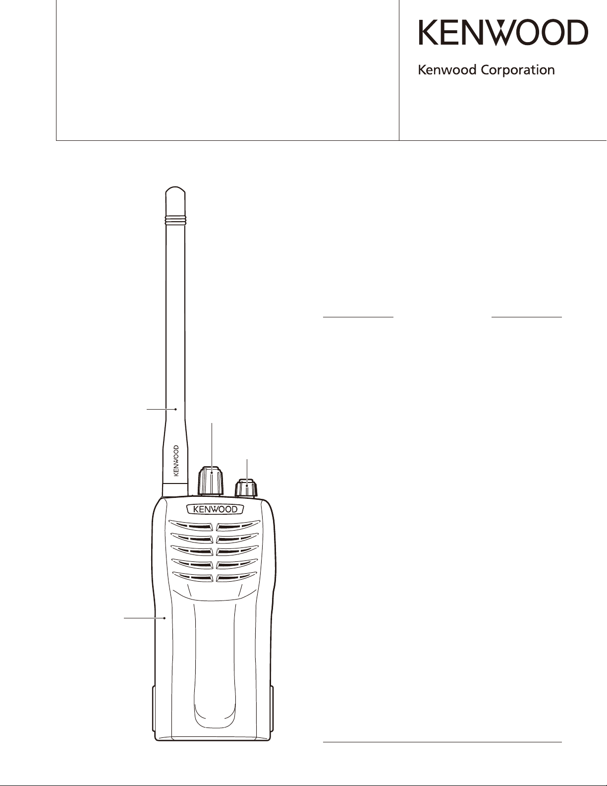
Helical antenna / 天线
(T90-1036-15)
Plastic cabinet assy
机壳(前面)
(A02-4049-13)
Knob (CH)
旋钮(信道)
(K29-5278-03)
Knob (Volume)
旋钮(音量)
(K29-5255-03)
REALIGNMENT ...........................................4
DISASSEMBLY FOR REPAIR ......................7
CIRCUIT DESCRIPTION ..............................9
SEMICONDUCTOR DATA .........................15
COMPONENTS DESCRIPTION .................17
PARTS LIST ...............................................19
EXPLODED VIEW ......................................25
PACKING ....................................................26
ADJUSTMENT ..........................................27
PC BOARD
TX-RX UNIT (X57-6020-10) ...................34
SCHEMATIC DIAGRAM ............................38
BLOCK DIAGRAM .....................................42
LEVEL DIAGRAM ......................................44
OPTIONAL ACCESSORIES
KNB-14 (Ni-Cd battery pack) ................45
KNB-15A (Ni-Cd battery pack) .............45
KNB-20N (Ni-MH battery pack) ............45
SPECIFICATIONS ..................... BACK COER

TK-2107G
目 录
概 述 ........................................................................ 3
系统体系 ........................................................................ 4
模式组合 ........................................................................ 4
维修拆卸 ........................................................................ 7
电路说明 ........................................................................ 9
半导体数据 .................................................................16
元件说明 ......................................................................17
零 件 表 ......................................................................19
部件分解图 .................................................................25
包 装 ......................................................................26
调 整 ......................................................................27
PC 板
TX-RX 单元 (X57-6020-10) .........................34
原 理 图 ......................................................................38
方 块 图 ......................................................................42
电 平 图 ......................................................................44
可选附件
KNB-14(镍镉电池) .........................................45
KNB-15A(镍镉电池) ......................................45
KNB-20N(镍氢电池) .....................................45
规 格 ................................................................. 封底
Document Copyrights
Copyright 2009 by Kenwood Corporation. All rights re-
served.
No part of this manual may be reproduced, translated,
distributed, or transmitted in any form or by any means,
electronic, mechanical, photocopying, recording, or otherwise, for any purpose without the prior written permission
of Kenwood.
Disclaimer
While every precaution has been taken in the preparation
of this manual, Kenwood assumes no responsibility for errors or omissions. Neither is any liability assumed for damages resulting from the use of the information contained
herein. Kenwood reserves the right to make changes to any
products herein at any time for improvement purposes.
2
文档版权信息
Kenwood Corporation 拥有版权 2009。保留所有权利。
未经 Kenwood公司预先书面同意,无论出于何种目的,均
不得以任何形式或任何方式包括电子、机械、影印、录音或
其他方式复制、翻译、分发或传播本手册的任何部分。
免责声明
Kenwood 公司在准备本文档时已采取所有必要的预防措施,
恕不对错误或疏漏承担任何责任,也不对因使用本文中所含
的信息而导致的损害负责。Kenwood 公司保留出于改进的需要
而随时对文中的产品信息做出更改的权利。

TK-2107G
GENERAL /
INTRODUCTION
SCOPE OF THIS MANUAL
This manual is intended for use by experienced tech ni cians familiar with similar types of commercial grade com mu ni ca tions equipment. It contains all required service
in for ma tion for the equipment and is current as of the publication date. Changes which may occur after publication
are covered by either Service Bulletins or Manual Revisions.
These are is sued as required.
ORDERING REPLACEMENT PARTS
When ordering replacement parts or equipment in for ma tion, the full part identifi cation number should be in clud ed.
This applies to all parts : components, kits, or chassis. If the
part number is not known, include the chassis or kit number
of which it is a part, and a suffi cient description of the re quired component for proper identifi cation.
PERSONAL SAFETY
The following precautions are recommended for personal
safety:
• DO NOT transmit until all RF connectors are verifi ed se -
cure and any open connectors are properly terminated.
• SHUT OFF and DO NOT operate this equipment near
elec tri cal blasting caps or in an explosive atmosphere.
• This equipment should be serviced by a qualifi ed tech ni -
cian only.
概述
引言
本手册的范围
本手册是提供给熟悉通信专业并且具有维修经验的技术人
员使用的。它包括了维修该设备所需要的全部资料和现行出
版日期。在出版后可能发生变动,如果需要,可以参照《维
修通报》或《手册修订本》进行补充。
替换零件的订购
当订购替换零件或设备资料时,应注意完整的零件识别号
码。所有的零件均有识别号码∶元件,组件或机壳。如果不
知道零件的号码,为了正确地识别,必须注明此元件所属的
机壳或组件的号码,并对元件进行充分的说明。
个人安全
为了个人的安全,请注意下列事项∶
• 在没有认真核实所有射频插头之前或有任何一个脱开的插
头没有连接到相应端口上的情况下均不要发射。
• 在电爆管附近或在易燃性气体环境中,必须关闭电源,不
要操作本设备。
• 本设备只应该由有资格的技术人员进行维修。
SERVICE
This transceiver is designed for easy servicing. Refer to
the sche mat ic diagrams, printed circuit board views, and
align ment procedures contained within.
Model Type TX-RX unit
TK-2107G C X57-6020-10 150~174MHz
Frequency range
Remarks
IF1: 38.85MHz
LOC: 38.4MHz
维修服务
为了便于维修本设备,建立了完整的维修服务体系,提供
了包括原理图,印刷电路板图和调整步骤在内的资料供参考。
型号 类型 TX-RX 单元
TK-2107G C X57-6020-10 150~174MHz
频率范围
备注
IF1:38.85MHz
LOC:38.4MHz
3
TK-2107G
SYSTEM SET-UP /
Merchandise received
接收订单
Choose the type of transceiver
Transceiver programming
Are you using the speaker microphone?
对讲机
选择
您使用扬声器话筒吗 ?
的类型
对讲机
编程
NO / 不 ( Option / 可选件)
Delivery
交货
系统体系
Frequency range (MHz)
频率范围(MHz)
TX/RX 150~174
A personal computer, programming interface (KPG-22/22A),
and FPU (programming software) are required for programming.
(The frequency, TX power HI/LOW, and signalling data are
programmed for the transceiver.)
编程时需要个人计算机,编程接口(KPG-22/22A)和FPU(编程软件)。
对讲机
(为
YES / 是
设定频率,常规系统特性,TX高/低功率,以及信令数据。)
KMC-17 or KMC-21 Speaker microphone
KMC-17或KMC-21扬声器话筒
RF power
射频功率
5.0W TK-2107G (C)
Type
类型
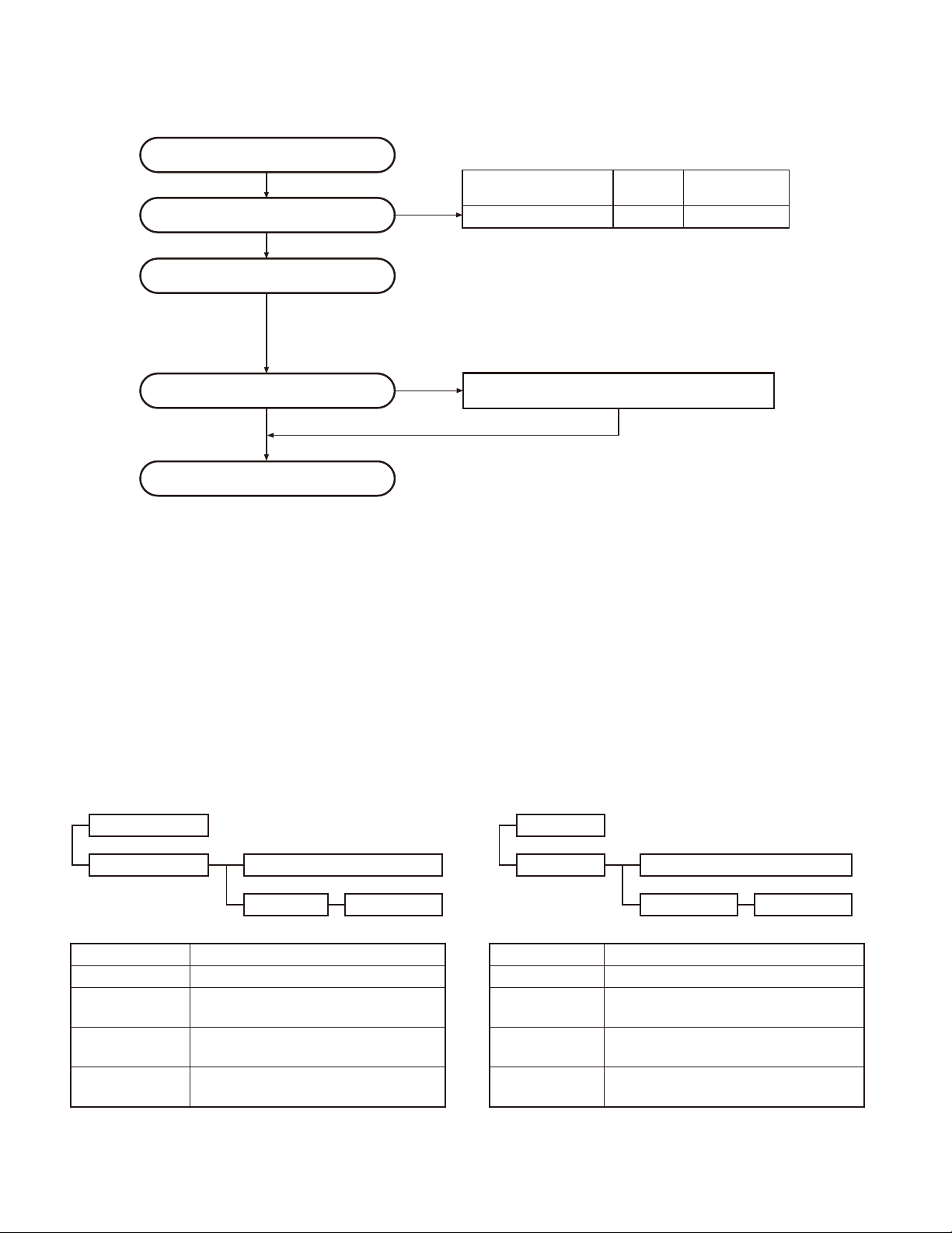
1. Modes
User mode
PC mode
PC test mode
Mode Function
User mode For normal use.
PC mode
Data programming
mode
PC test mode
Used for communication between the transceiver and PC.
Used to read and write frequency data and
other features to and from the transceiver.
Used to check the transceiver using the PC.
This feature is included in the FPU.
REALIGNMENT /
Data programming mode
PC tuning mode
模式组合
1. 模式
用户模式
计算机模式
计算机测试模式
模 式 功 能
用户模式 一般使用
计算机模式 用户对讲机与计算机之间的通信。
数据编程模式 用于读出和写入频率数据以及其他功能。
计算机测试模式
用于使用计算机来检测对讲机。此功能包
括在 FPU。
数据编程模式
计算机调谐模式
4

TK-2107G
REALIGNMENT /
2. How to Enter Each Mode
Mode Operation
User mode Power ON
PC mode Received commands from PC
3. PC Mode
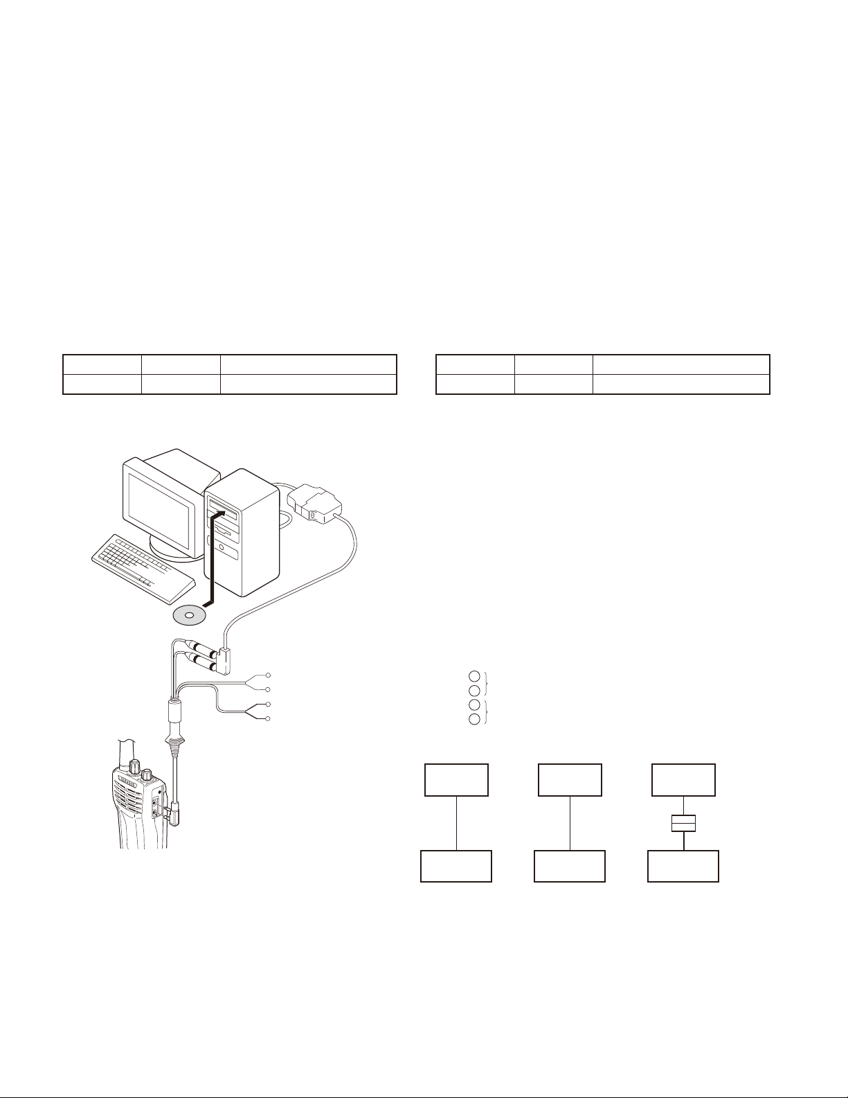
3-1. Preface
The transceiver is programmed by using a personal computer, a programming interface (KPG-22/22A, USB adapter
(KCT-53U)) and FPU (programming software).
The programming software can be used with a PC. Figure
1 shows the setup of a PC for programming.
3-2. Connection Procedure
1. Connect the transceiver to the personal computer with
the interface cable and USB adapter (when the interface
cable is KPG-22A, the KCT-53U can be used).
Note:
• You must install the KCT-53U driver in the computer to
use the USB adapter (KCT-53U).
• When using the USB adapter (KCT-53U) for the fi rst time,
plug the KCT-53U into a USB port on the computer with
the computer power ON.
模式组合
2. 如何进入每一种模式
模 式 操 作
用户模式 接通电源
计算机模式 从计算机接收指令
3. PC 模式
3-1. 前言
对讲机采用个人电脑、编程接口 (KPG-22/22A,USB 适配器
(KCT-53U)) 和 FPU( 编程软件 ) 进行编程。
编程软件可以在 PC 上进行使用。图 1 给出了 P C 进行编程
的设置。
3-2. 连接操作
1. 使用接口电缆和 USB 适配器将对讲机连接到个人电脑 ( 接
口电缆为 KPG-22A 时,可以使用 KCT-53U)。
注意 :
• 必须在电脑上安装 K CT -53U 驱动程序才能使用 U S B 适配器
(KCT-53U)。
• 首次使用 U S B 适配器 (KCT-53U) 时,请在电脑开机的情况
下将 KCT-53U 插入电脑的 USB 端口。
2. When the POWER is switched on, user mode can be entered immediately. When the PC sends a command, the
transceiver enters PC mode.
When data is read from the transceiver, the red LED
lights.
When data is written to by the transceiver, the green LED
lights.
Note:
• The data stored in the personal computer must match
Model Name and Model Type when it is written into EEPROM.
• Do not press the [PTT] key during data transmission or
reception.
3-3. KPG-22/KPG-22A Description
(PC programming interface cable : Option)
The KPG-22/22A is required to interface the transceiver
with the computer. It has a circuit in its D-sub connector
(KPG-22: 25-pin, KPG-22A: 9-pin) case that converts the RS232C logic level to the TTL level.
The KPG-22/22A connects the SP/MIC connector of the
transceiver to the RS-232C serial port of the computer.
3-4. KCT-53U Description (USB adapter : Option)
The KCT-53U is a cable which connects the KPG-22A to a
USB port on a computer.
When using the KCT-53U, install the supplied CD-ROM
(with driver software) in the computer. The KCT-53U driver
runs under Windows 2000 or XP.
2. 对讲机电源打开时,可以立即进入用户模式。 PC 发送指令
时,对讲机进入 PC 模式。
对讲机发送数据时,红色的 LED 点亮。
对讲机接收数据时,绿色的 LED 点亮。
注意 :
• 个人电脑保存的数据写入 EEPROM 时,必须与机型和类型相
符。
• 请勿在数据发送或接收期间按 [PTT] 键。
3-3. KPG-22/KPG-22A 说明
(PC 编程接口电缆 :选购件 )
将对讲机与电脑相连需要 KPG -22/22A。该电缆的 D-sub 连
接器 (KPG-22 :25 针,KPG-22A :9 针 ) 盒具有将 RS-232C 逻
辑电平转换为 TTL 电平的电路。
KP G -22/22A 将对讲机的 SP/MIC 连接器连接到电脑的 RS -
232C 串行端口。
3-4. KCT-53U 说明 (USB 适配器 :选购件 )
KCT-53U 是将 KPG-22A 连接到电脑 USB 端口的电缆。
使用 KCT-53U 时,请在电脑上安装附带的 CD-ROM( 带有驱
动程序软件 )。KCT-53U 驱动程序运行于Windows 2000 或XP 下。
5
TK-2107G
REALIGNMENT /
3-5. FPU (Programming Software) Description
The FPU is the programming software for the transceiver
supplied on a CD-ROM. The software on this disk allows a
user to program the transceiver transceivers via Programming interface cable (KPG-22/22A).
3-6. Programming with PC
If data is transferred to the transceiver from a PC with the
FPU, the data for each set can be modifi ed.
Data can be programmed into the EEPROM in RS-232C
format via the SP/MIC jack.
In this mode the PTT line operate as TXD and RXD data
lines respectively.
List of FPU for transceiver
Model Type FPU
TK-2107G C KPG-55D
KPG-22 or KPG-22A or KPG-22A+KCT-53U
KPG-22或KPG-22A或KPG-22A+KCT-53U
PC
Illustration is KPG-22
插图为KPG-22
模式组合
3-5. FPU( 编程软件 ) 说明
FPU 是 CD-ROM 附带的用于对讲机的编程软件。该光盘上的
软件允许用户通过编程接口电缆 (KPG-22/22A) 对对讲机进行
编程。
3-6. 使用 PC 编程
如果使用 FPU 将数据从 PC 传输到对讲机,则每套对讲机的
数据均可修改。
通过 SP/MIC 插孔可以将数据以 RS-232C 格式写入 EEPROM。
在该模式下,PTT 线路分别用作 TXD 和 RXD 数据线路。
对讲机的 FPU 名单
型 号 类 型
TK-2107G C KPG-55D
FPU
FPU
Tuning cable / 调谐电缆
(E30-3216-05)
Gray
Gray/Black
1.5D-XV Lead wire
1.5D-XV Shield wire
灰色
灰色/黑色
1.5D-XV导线
1.5D-XV屏蔽线
(25-pin)
Transceiver
Fig. 1 /
图1
PC
D-SUB
对讲机
+
SP
–
+
MIC
–
KPG-22
PC
D-SUB
(9-pin)
KPG-22A
Transceiver
对讲机
PC
USB
KCT-53U
KPG-22A
Transceiver
对讲机
6
TK-2107G
DISASSEMBLY FOR REPAIR /
1.
Removing the Case Assembly from the Chassis
1. Remove the two knobs (q), cushion (w) and three round
nuts (e).
2. Remove the two screws (r).
3. Expand the right and left sides of the bottom of the case
assembly, Iift the chassis, and remove it from the case
assembly (t).
4. Taking care not to cut the speaker lead (y), open the
chassis and case assembly.
Note: Solder the speaker wire back in its original position if
you have removed it.
;
;
.
:
:
@
.
.
维修拆卸
1. 拆卸机壳
1. 取下旋扭 (q),缓冲垫 (w) 和两个环形螺母 (e)。
2. 取下两颗螺钉 (r)。
3. 掀开外壳底部的左右两侧,取下底座,并外壳中取出 (t)。
4. 小心不要折断扬声器引线 (y)。拆下底座和外壳。
注意 :
如果取下了扬声器的导线,请将其焊接到原位上。
B
=
2.
Removing the TX-RX unit from the Chassis
1. Remove the eleven screws (u).
2. Remove the FPC from connector (CN400) (i).
3. Remove the solder from the antenna terminal using a soldering iron then lift the unit off (o).
4. Remove the waterproof packing (!0) and cushion (!1)
from the antenna connecor.
5. Remove the two screws (!2) and remove the antenna
connector.
Note: When reassembling the unit in the chassis, be sure
to solder the antenna terminal.
>
>
>
>
2. 拆卸 TX-RX 单元
1. 取下 11 颗螺钉 (u)。
2. 从连接器 (CN400) 取下 FPC(i)。
3. 用电烙铁将天线端点焊开,然后取下主板 (o)。
4. 从天线连接器取下防水橡胶圈 (!0) 和树脂垫片 (!1)。
5. 取下两颗螺钉 (!2) 并取下天线连接器。
注意 :
当重新将主板安装到底座上时,确保将天线端点焊好。
8
Antenna terminal
天线端点
>
>
>
>
>
>
2
CN400
7
TK-2107G
DISASSEMBLY FOR REPAIR /
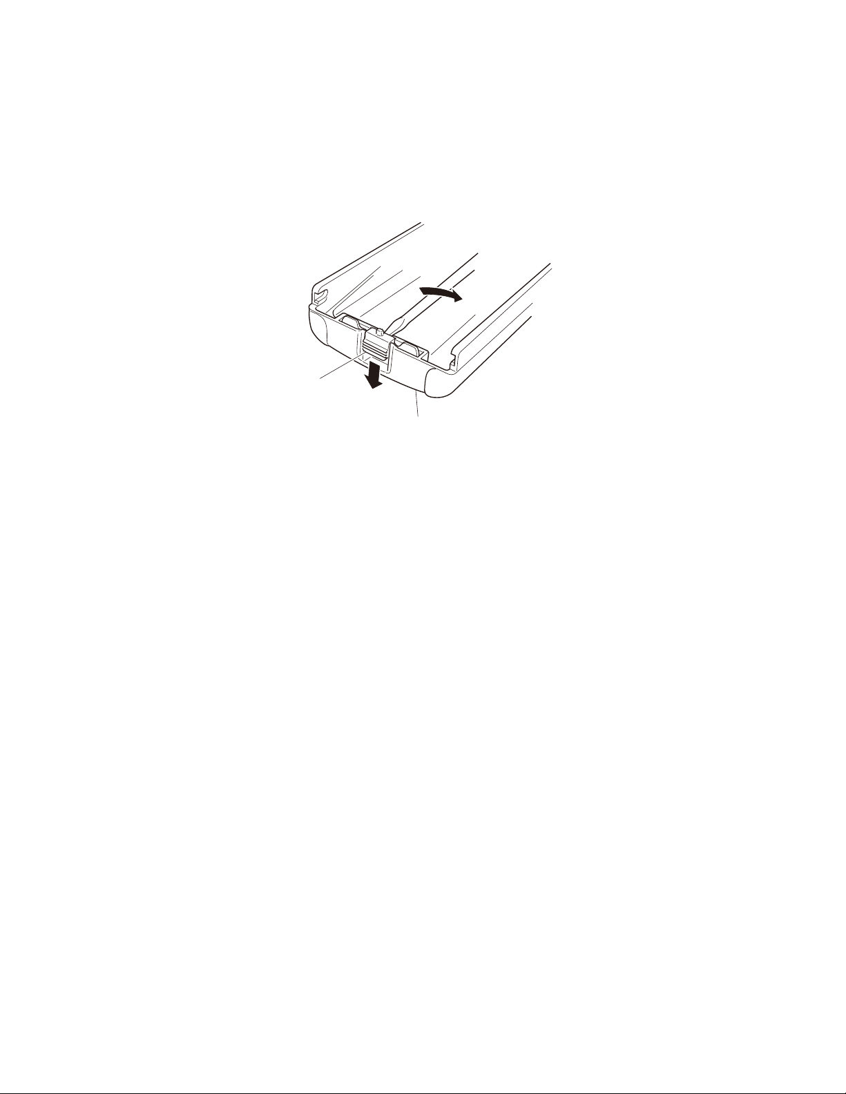
3. Removing the lever
1. Raise the lever on the lower case (!3), insert a small fl at
screwdriver into the space between the case and lever,
open the case carefully (!4) and lift the lever off.
Note: Do not force to separate the case from the lever.
Lever knob
锁扣
Case assembly
维修拆卸
3. 取下夹扭
1. 提起在外壳下部 (!3) 上的锁扣,在外壳和锁扣之间插入一
个小型平头改锥,小心地打开外壳 (!4) 并卸下锁扣。
注意 :
不要用力拆卸锁扣和外壳。
外壳
8
TK-2107G
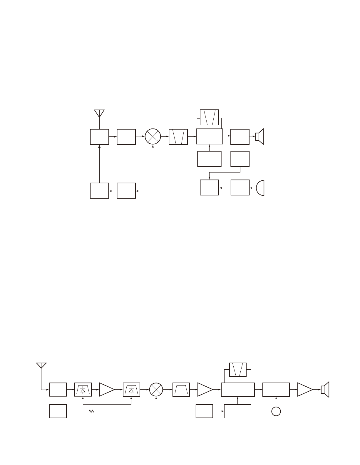
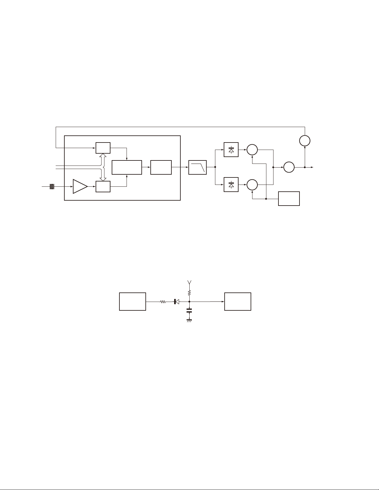
CIRCUIT DESCRIPTION /
1. Frequency Confi guration
The receiver utilizes double conversion. The first IF is
38.85MHz and the second IF is 450kHz. The fi rst local oscillator signal is supplied from the PLL circuit.
The PLL circuit in the transmitter generates the neces-
sary frequencies. Fig. 1 shows the frequencies.
ANT
150~174MHz
ANT
SW
PA
AMP
RF
AMP
TX
AMP
38.85MHz
RX
188.85~212.85MHz
TX 150~174MHz
MCF
电路说明
1. 频率构成
接收部采用二次变频超外差方式。第一中频为 38.85MH z,
第二中频为 450K H z。第一本振频率信号由锁相环电路 (PLL)
提供。
发射部由锁相环电路直接产生所需要的频率。图 1 显示各
种频率。
CF
450kHz
IF
SYSTEM
38.4MHz
X3
multiply
PLL
VCO
AF
AMP
TCXO
MIC
AMP
SP
12.8MHz
MIC
Fig. 1 Frequency confi guration /
2. Receiver
The frequency confi guration of the receiver is shown in
Fig. 2.
2-1. Front-end RF amplifi er
An incoming signal from the antenna is applied to an RF
amplifier (Q203) after passing through a transmit/receive
switch circuit (D102 and D103 are off) and a band pass fi lter
(L208, L209 and L210). After the signal is amplifi ed (Q203),
the signal is filtered through a band pass filter (L203 and
L214) to eliminate unwanted signals before it is passed to
the fi rst mixer. Band pass fi lters (L208, L209, L210, L203
and L214) have varactor diodes (D203, D204, D205, D202
and D201).
The voltage of these diodes are controlled by to track the
MCU (IC403) center frequency of the band pass fi lter. (See
Fig. 2)
ANT
D102,
D103
ANT
SW
IC403
MCU
BPF
L208~L210
APC
RF AMP
Q203
TUNE
BPF
L214,L203
MIXER
Q202
1st Local OSC
(PLL)
图 1 电路构成
2. 接收部
接收部的频率构成如图 2 所示。
2-1. 前端射频放大器
从天线输入的信号经过收发转换电路 (D102 和 D103 断
开 ) 和带通滤波器 (L208,L209 和 L210) 后,在射频放大器
( Q203) 处放大。信号被放大后 (Q203),在通过第一混频器之
前,经过带通滤波器 ( L203 和 L214) 滤波来消除不要的信号。
带通滤波器 (L208, L209, L210,L203 和 L214) 有变容二极管
(D203,D204,D205,D202 和 D201)。
这些变容二极管的电压由带通滤波器的 MCU(IC403) 中心频
率控制。( 参见图 2)
CF200
MCF
XF200
IF AMP
Q201
TCXO
IF, MIX, DET
IC200
X3
multiply
Q1
IC300
AF AMP
LPF, HPF
AF PA AMP
Wide/Narrow SW
Q303
IC302
SP
Fig. 2 Receiver section confi guration /
图 2 接收部构成
9
TK-2107G
CIRCUIT DESCRIPTION /
2-2. First mixer
The signal from the RF amplifi er is heterodyned with the
fi rst local oscillator signal from the PLL frequency synthesizer circuit at the fi rst mixer (Q202) to create a 38.85MHz
fi rst intermediate frequency (1st IF) signal. The fi rst IF signal
is then fed through two monolithic crystal filters (MCFs :
XF200) to further remove spurious signals.
2-3. IF amplifi er
The fi rst IF signal is amplifi ed by Q201, and then enters
IC200 (FM processing IC). The signal is heterodyned again
with a second local oscillator signal within IC200 to create
a 450kHz second IF signal. The second IF signal is then fed
through a 450kHz ceramic fi lter (CF200) to further eliminate
unwanted signals before it is amplifi ed and FM detected in
IC200.
XF200: L71-0522-05
Item Rating
Nominal center frequency 38.850MHz
Pass band width ±5.0kHz or more at 3dB
40dB stop band width ±20.0kHz or less
Ripple 1.0dB or less
Insertion loss 4.0dB or less
Guaranteed attenuation 80dB or more at fo–910kHz
Terminal impedance 610Ω / 3pF
电路说明
2-2. 第一混频器
来自射频放大器的信号与来自锁相环频率合成器电路的第
一本振信号在第一混频器 (Q202) 处混频并生成 38.85M Hz 的
第一中频 (1st IF) 信号。第一中频信号通过两个单片晶体滤
波器 (MCFs: XF200) 进一步消除邻道的杂波信号。
2-3. 中频放大器
第一中频信号通过 Q201 放大,然后进入芯片 I C200( 调频
处理芯片 )。信号在 IC200 中与第二本振信号再次混频生成一
个 450kH z 的第二中频信号。在芯片 IC200 中第二本振信号被
放大和鉴频之前,通过一个 450kHz 陶瓷滤波器 (CF200) 滤除
无用杂散信号。
XF200: L71-0522-05
项 目 额 定 值
标称中心频率 38.850MHz
通频带宽 ±5.0kHz 或更大在 3dB 内
40dB 止频带宽 ±20.0kHz 或更小
脉动 1.0dB 或更小
插入损耗 4.0dB 或更小
保证衰减 80dB 或更大
终端阻抗 610Ω/3pF
CF200: L72-0958-05
Item Rating
Nominal center frequency 450kHz
6dB band width ±6.0kHz or more
50dB band width ±12.5kHz or less
Ripple 2.0dB or less at fo ±4kHz
Insertion loss 6.0dB or less
Guaranteed attenuation 35.0dB or more at fo ±100kHz
Terminal impedance 2.0k
Ω
2-4. AF amplifi er
The recovered AF signal obtained from IC200 is amplifi ed
by IC300 (1/4), fi ltered by the IC300 low-pass fi lter (2/4) and
IC300 high-pass filter (3/4) and (4/4), and de-emphasized
by R303 and C306. The AF signal is then passed through a
WIDE/NARROW switch (Q303). The processed AF signal
passes through an AF volume control and is amplifi ed to a
suffi cient level to drive a loud speaker by an AF power amplifi er (IC302).
CF200: L72-0958-05
项 目 额 定 值
标称中心频率 450kHz
6dB 频带宽度 ±6.0kHz 或更大
50dB 频带宽度 ±12.5kHz 或更小
脉动 2.0dB 或更小
插入损耗 6.0dB 或更小
保证衰减 35.0dB 或更大
终端阻抗 2.0kΩ
2-4. 音频放大器
在 I C200 中鉴频解调出的音频信号通过 I C300(1/4) 放大,
通过 I C300 低通滤波器 (2/4) 以及 IC300 高通滤波器 (3/4)
和 (4/4) 滤波,并且通过 R303 和 C306 去加重。然后音频信
号通过一个宽 / 窄转换开关 ( Q303)。经过处理的音频信号通
过音量控制电路再经过音频功率放大器 ( IC302) 放大后、驱
动扬声器。
10
TK-2107 G
CIRCUIT DESCRIPTION /
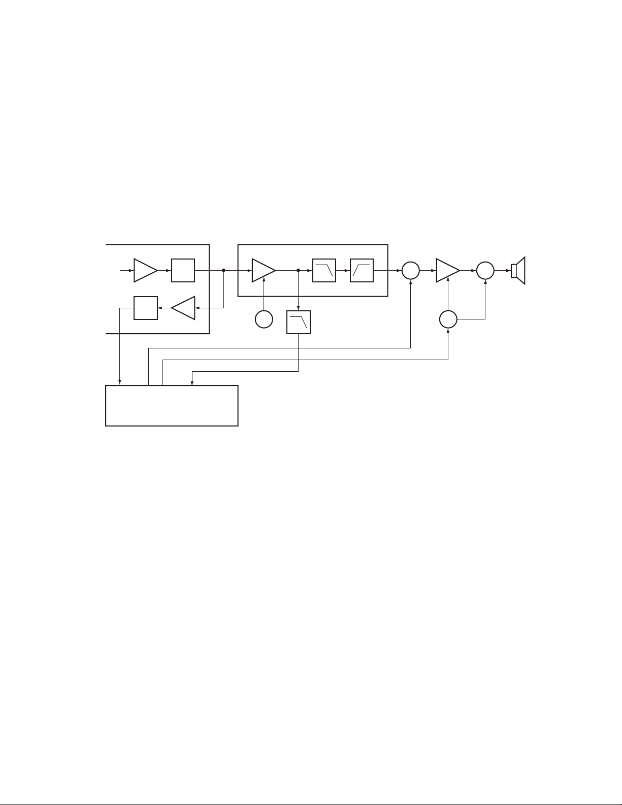
2-5. Squelch
Part of the AF signal from the IC enters the FM IC again,
and the noise component is amplifi ed and rectifi ed by a fi lter
and an amplifi er to produce a DC voltage corresponding to
the noise level.
The DC signal from the FM IC goes to the analog port of
the microprocessor (IC403). IC403 determines whether to
output sounds from the speaker by checking whether the
input voltage is higher or lower than the preset value.
To output sounds from the speaker, IC403 sends a high
signal to the MUTE and AFCO Iines and turns IC302 on
through Q302, Q304, Q305, Q306 and Q307. (See Fig. 3)
IC200: FM IF IC
IF AMP
DET
HPF AMP
DET
AF AMP
Q303
W/N SW
电路说明
2-5. 噪音抑制电路
从 I C200 输出的音频信号的一部分重新进入 IC200,通过
滤波器和放大器将噪音放大和整流并生成一个对应于噪音电
平的直流电压。直流信号进入微处理器的模拟端口 (I C403)。
IC403 通过检测输入电压是否高于或低于预设值来决定是否通
过扬声器输出声音。
要通过扬声器输出声音,IC403 向静音和自动频率控制振
荡器连线发送一个高电平信号并开启 I C302 通过 Q302, Q304,
Q305,Q306 和 Q307。( 参见图 3)
IC300
LPF HPF
IC301
LPF
QT/DQT
Q302
SW
IC302
AF PA AMP
Q304~Q306
Q307
SW
SW
SP
6
BUSY
67
MUTE
62
AFCO
5
TI
IC403
MCU
Fig. 3 AF amplifi er and Squelch /
2-6. Receive signaling
• QT/DQT
300Hz and higher audio frequencies of the output signal
from IF IC are cut by a low-pass fi lter (IC301). The resulting
signal enters the microprocessor (IC403). IC403 determines
whether the QT or DQT matches the preset value, and controls the MUTE and AFCO and the speaker output sounds
according to the squelch results.
3. PLL Frequency Synthesizer
The PLL circuit generates the fi rst local oscillator signal
for reception and the RF signal for transmission.
3-1. PLL
The frequency step of the PLL circuit is 5 or 6.25kHz. A
12.8MHz reference oscillator signal is divided at IC1 by a
fixed counter to produce the 5 or 6.25kHz reference frequency. The voltage controlled oscillator (VCO) output signal
is buffer amplifi ed by Q6, then divided in IC1 by a dual-module programmable counter. The divided signal is compared
in phase with the 5 or 6.25kHz reference signal in the phase
comparator in IC1. The output signal from the phase comparator is fi ltrered through a low-pass fi lter and passed to
the VCO to control the oscillator frequency. (See Fig. 4)
图 3 音频放大器和噪音抑制电路
2-6. 接收信令
•
QT/DQT
来自于中频芯片输出信号的 300Hz 和更高的音频被低频
滤波器 ( Q301) 截断。所得到的信号输入微处理器 (IC403)。
I C403 确定 QT 或 D QT 是否匹配预设置,并且根据噪声抑制电
路的结果控制 MUTE 和 AFCO 以及扬声器输出声音。
3. 锁相环频率合成器
锁相环电路生成用于接收的第一本振信号和用于发送的射
频载波信号。
3-1. 锁相环电路
锁相环电路的步进频率为 5 或 6.25k H z。12.8MHz 的 参考
振荡器信号通过一个混合计数器在 IC1 中被分频并生成 5 或
6.25k H z 的参考频率。压控振荡器 (VCO)输出的信号通过 Q6
缓冲放大器,然后在 I C1 中被可编程脉冲吞除计数器分频。
被分频的信号在带有 5 或 6.25kH z 参考信号的相位比较器的
IC1 中被比较。从相位比较器输出的信号进入一个低通滤波器
后,并通过压控振荡器来控制振荡频率。( 参见图 4)
11
TK-2107G
CIRCUIT DESCRIPTION /
3-2. VCO
The operating frequency is generated by Q4 in transmit
mode and Q3 in receive mode. The oscillator frequency is
controlled by applying the VCO control voltage, obtained
from the phase comparator, to the varactor diodes (D1 and
D2 in transmit mode and D3 and D4 in receive mode). The
T/R pin is set high in receive mode causing Q5 and Q7 to
turn Q4 off, and turn Q3 on . The T/R pin is set low in transmit mode. The outputs from Q3 and Q4 are amplifi ed by Q6
and sent to the buffer amplifi ers.
IC1: PLL IC
5kHz/6.25kHz
1/N
PLL
data
REF OSC
1/M
12.8MHz
Phase
comparator
5kHz/6.25kHz
Charge
pump
电路说明
3-2. 压控振荡器
在发射模式中通过 Q4 产生操作频率,在接收模式中通过
Q3 产生操作频率。通过相位比较器到变容二极管 ( 在发射模
式中为 D1 和 D2,在接收模式中为 D3 和 D4) 采用压控振荡器
控制电压来控制振荡频率。在接收模式中,由于 Q5 和 Q7 切
断 Q4 并且导通 Q3,所以发射 / 接收管脚设置为高电平。在发
射模式中,发射 / 接收管脚设置为低电平。Q3 和 Q4 的输出通
过 Q6 被放大并被发送到缓冲放大器。
D1,2
LPF
D3,4
Q4
TX VCO
Q3
RX VCO
Q2
RF AMP
Q6
BUFF AMP
Q5,7
T/R SW
Fig. 4 PLL circuit /
3-3. Unlock detector
If a pulse signal appears at the LD pin of IC1, an unlock
condition occurs, and the DC voltage obtained from D7, R1,
and C1 causes the voltage applied to the UL pin of the microprocessor to go low. When the microprocessor detects
this condition, the transmitter is disabled, ignoring the pushto-talk switch input signal. (See Fig. 5)
IC1
PLL IC
D7
LD
Fig. 5 Unlock detector circuit /
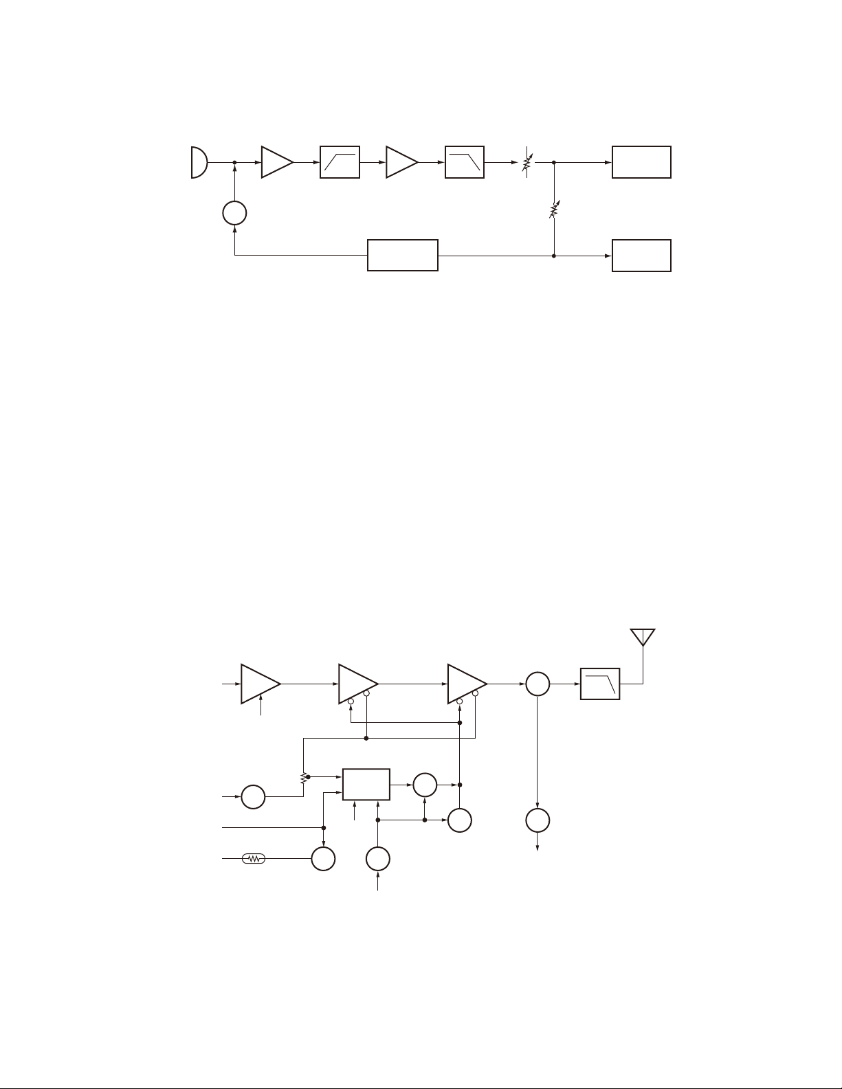
4. Transmitter
4-1. Transmit audio
The modulation signal from the microphone is amplifi ed
by IC500 (1/2), passes through a preemphasis circuit, and
amplifi ed by the other IC500 (1/2) to perform IDC operation.
The signal then passes through a low-pass filter (splatter
fi Iter) (Q501 and Q502) and cuts 3kHz and higher frequencies. The resulting signal goes to the VCO through the VCO
modulation terminal for direct FM modulation. (See Fig. 6)
图 4 锁相环电路
3-3. 失锁检测器
如果 IC1 的 LD 管脚上出现高电平,则产生失锁状态,并从
D7,R1 获得直流电压,且 C1 产生的提供给微处理器 UL 管脚的
电压降低。当微处理器检测到此情况时,不能进行发射,无
视通话转换开关输入信号。( 参见图 5)
5C
R1
C1
IC403
MCU
UL
图 4 失锁检测器电路
4. 发射部
4-1. 发射音频
来自于话筒的调制信号通过 I C500(1/2) 被放大,经过一个
预加重电路,并通过另一个 IC500(1/2) 放大后进行 IDC 处理。
然后信号通过一个低通滤波器 ( 分离滤波器 ) ( Q501 和 Q502)
并滤除比 3k H z 频率更高的部分。得到的信号进入压控振荡器
直接进行调频调制。( 参见图 6)
4-2. QT/DQT encoder
A necessary signal for QT/DQT encoding is generated by
IC403 and FM-modulated to the PLL reference signal. Since
the reference OSC does not modulate the loop characteristic frequency or higher, modulation is performed at the VCO
side by adjusting the balance. (See Fig. 6)
12
4-2. QT/DQT 编码器
QT/DQT 编码所需的信号通过 IC403 产生,被锁相环电路的
基准频率调整。由于基准振荡器不能对频率环路特性外的频
率进行调制,因此通过分配器在压控振荡器一侧进行调制。(参
见图 6)
TK-2107G
CIRCUIT DESCRIPTION /
MIC
IC500 (1/2)
MIC AMP
Pre-emphasis
Q503
SW
Fig. 6 Transmit audio QT/DQT /
4-3. VCO and RF amplifi er
The transmit signal obtained from the VCO buffer amplifier Q100, is amplified by Q101. This amplified signal is
passed to the power amplifi er, Q102 and Q105, which consists of a 2-stage FET amplifi er and is capable of producing
up to 5W of RF power. (See Fig. 7)
IC500 (1/2)
IDC
IC403
MCU
MUTE
电路说明
Q501,502
LPF
(Splatter filter)
QT/DQT
TO
图 6 发射音频 QT/DQT
4-3. 压控振荡器和射频放大器
从压控振荡缓冲放大器 (Q100) 接收到的发送信号通过 Q101
被放大。这个放大信号通过功率放大器,Q102 和 Q105( 包括
一个二级场效应管放大器 ),并能产生 4W射频功率。( 参见图 7)
VR501
MAX DEV
D5, Q4
VCO
VR500
Balance
X1, IC1
Reference
OSC
(TCXO)
4-4. ANT switch and LPF
The RF amplifi er output signal is passed through a lowpass fi lter network and a transmit/receive switching circuit
before it is passed to the antenna terminal. The transmit/
receive switching circuit is comprised of D101, D102, D103
and D104. D102 and D103 are turned on (conductive) in
transmit mode and off (isolated) in receive mode.
AMP
Q101
5T
Q103,Q104
B SW
B
APC
TH100
5T
DRIVE AMP
DET
SW
Q107
Q102
APC
IC100
5T
SW
Q108
5T
4-4. 天线转换开关和 LPF
在其到达天线终端之前,射频放大器输出信号通过一个低
通滤波器网络和一个发射 / 接收转换电路。发射 / 接收转换
电路由 D101,D102,D103 和 D104 构成。D102 和 D103 在发射模
式下开启 ( 通导 ),在接收模式下关闭 ( 隔离 )。
ANT
SW
Q106
ANT SW
D101,104
RX
LPF
ANT SW
D102,103
FINAL AMP
Q105
SW
Q109
Fig. 7 APC system /
图 7 自动功率控制系统
13

TK-2107G
CIRCUIT DESCRIPTION /
4-5. APC
The automatic power control (APC) circuit stabilizes the
transmitter output power at a predetermined level by sensing the drain current of the fi nal amplifi er Field Effect Transistor (FET). The voltage comparator, IC100 (2/2), compares
the voltage obtained from the above drain current with a
reference voltage which is set using the microprocessor.
An APC voltage proportional to the difference between the
sensed voltage and the reference voltage appears at the
output of IC100 (1/2). This output voltage controls the gate
of the FET power amplifier, which keeps the transmitter
output power constant. The transmitter output power can
be varied by the microprocessor which in turn changes the
reference voltage and hence, the output power.
4-6. Terminal protection circuit
When the thermistor (TH100) reaches about 80˚C, the
protection circuit turns on Q107 to protect transmitting fi nal
amplifi er (Q105) from the over heating.
5. Power supply
A 5V reference power supply [5M] for the control circuit
is derived from an internal battery. This reference is used
to provide a 5V supply in transmit mode [5T], a 5V supply in
receive mode [5R], and a 5V supply common in both modes
[5C] based on the control signal sent from the microprocessor.
电路说明
4-5. 自动功率控制
自动功率控制 (APC) 电路,通过测检末级放大器场效
应管的集极电流来稳定发射的输出功率。电压比较电路,
I C100(2/2) 用微处理机设定的参考电压来比较从末级电流所
获得的电压。自动功率控制电压与 I C100(1/2) 输出的自动检
测电压和参考电压之间的差值成正比。此输出电压控制场效
应管功率放大器,保持发射部输出功率常数。发射部输出功
率可以通过微处理器进行改变,在微处理器中改变参考电压
来控制输出功率。
4-6. 温度保护电路
当热敏电阻 (TH100) 的温度达到 80℃时,保护电路开启
Q107 来保护末级放大器 (Q105) 避免过热。
5. 电源
为控制电路提供的 5V 参考电源 [5M] 源于一个内部电池。
此参考电源通常在发射模式中 [5T] 提供一个 5V 电源,在接
收模式中 [5R] 提供一个 5V 电源,并且在发自于微处理器的
控制信号的基础上,在两种模式中 [5C] 提供一个共用的 5V
电源。
6. Control system
The IC403 MCU operates at 7.37MHz. This oscillator has
a circuit that shifts the frequency according to the EEPROM
data.
6. 控制系统
I C403 微处理器在 7.37MH z 的情况下运行。此振荡器有一
个按照 EEPROM 的数据转移频率的电路。
14
SEMICONDUCTOR DATA
MCU: 38268MCA060GU (IC403)
Pin No. I/O
1 O VC1 Variable capacity tune control
2 O VC2 Variable capacity tune control
3 I NC NC
4 I TIBI
5 I TI QT/DQT signal input
6 I BUSY Busy input
7 l BATT Battery voltage detection
8 l NC NC
9 O VCCN Frequency regulation output
10 O APC
11~14 I NC NC
15 O BEEP Beep output
16 O TO QT/DQT output
17 l NC NC
18 I PTT [PTT] key input Connected to RXD
19 O TXD
20 I RXD RS-232C input Connected to [PTT] line
21 l NC NC
22 I SELF Self program L: Disable
23 I MONl [MONl] key input
24~27 I NC NC
28 l ENC3 Encode input (channel select)
29 l ENC2 Encode input (channel select)
30 l ENC1 Encode input (channel select)
31 l ENC0 Encode input (channel select)
32 l INTO Power detection control
33 I RST Reset input
34 I NC NC
35 O NC NC
36 l XIN 7.3728MHz oscillator
37 O XOUT 7.3728MHz oscillator
38 I VSS GND
39 O SHIFT Beat shift H: Shift on
40 O PABC Final supply H: On
41 O WNRC Audio reference sensitivity L: Narrow
42 O WNTC MAX Dev. Control Narrow: H
43~46 l NC NC
47 l/O SDA EEPROM data line
Port Name
Function
QT/DQT external circuit center point
input
TX: Auto power control D/A output
RX: BPF tuning D/A output
RS-232C output Connected to SP/MIC
test (REM)
TK-2107G
Pin No. I/O
48 O SCL EEPROM clock line
49 I UL PLL unlock detection pin L: Unlock
50~54 l NC NC
55 O DT Common data output
56 O CK Common clock output
57 O NC NC
58 O LE PLL IC enable H: Iatches
59,60 O NC NC
61 O 5MC
62 O AFCO AF amp power suppIy H: On
63 O RX TX/RX VCO select H: RX
64 O GLED Green LED control H: Lit
65 O RLED RED LED control H: Lit
66 O SAVE Save control H: Save off
67 O MUTE Mute control H: Mic mute, L: AF mute
68 O 5RC Reception power suppIy control L: On
69 O 5TC
70~88 O NC NC
89 l VCC Microcomputer power supply, 5V input
90 l VREF
91 l AVSS
92~95 O NC NC
96~100 I NC NC
FET: 2SK2596-E (Q102)
Absolute Maximum Ratings (Ta=25°C)
■
Item VDSS VGSS ID Pch Tch Tstg
Rating 17V ±10V 0.4A
FET: 2SK2595-E (Q105)
Absolute Maximum Ratings (Ta=25°C)
■
Item VDS VGSS ID Pch Tch Tstg
Rating 17V ±10V 1.1A
Port Name
Function
Control of power supply (5M) for everything except the microcomputer and
EEPROM L: Power supply on
Transmission power suppIy control
H: On
A/D conversion reference voltage; connected to Vcc
A/D converter power supply; connected
to Vss
3W
Tc=25°C
20W
Tc=25°C
150°C –45~+150°C
150°C –45~+150°C
15
 Loading...