

Page 1
VHF FM TRANSCEIVER
TK-2102G
SERVICE MANUAL
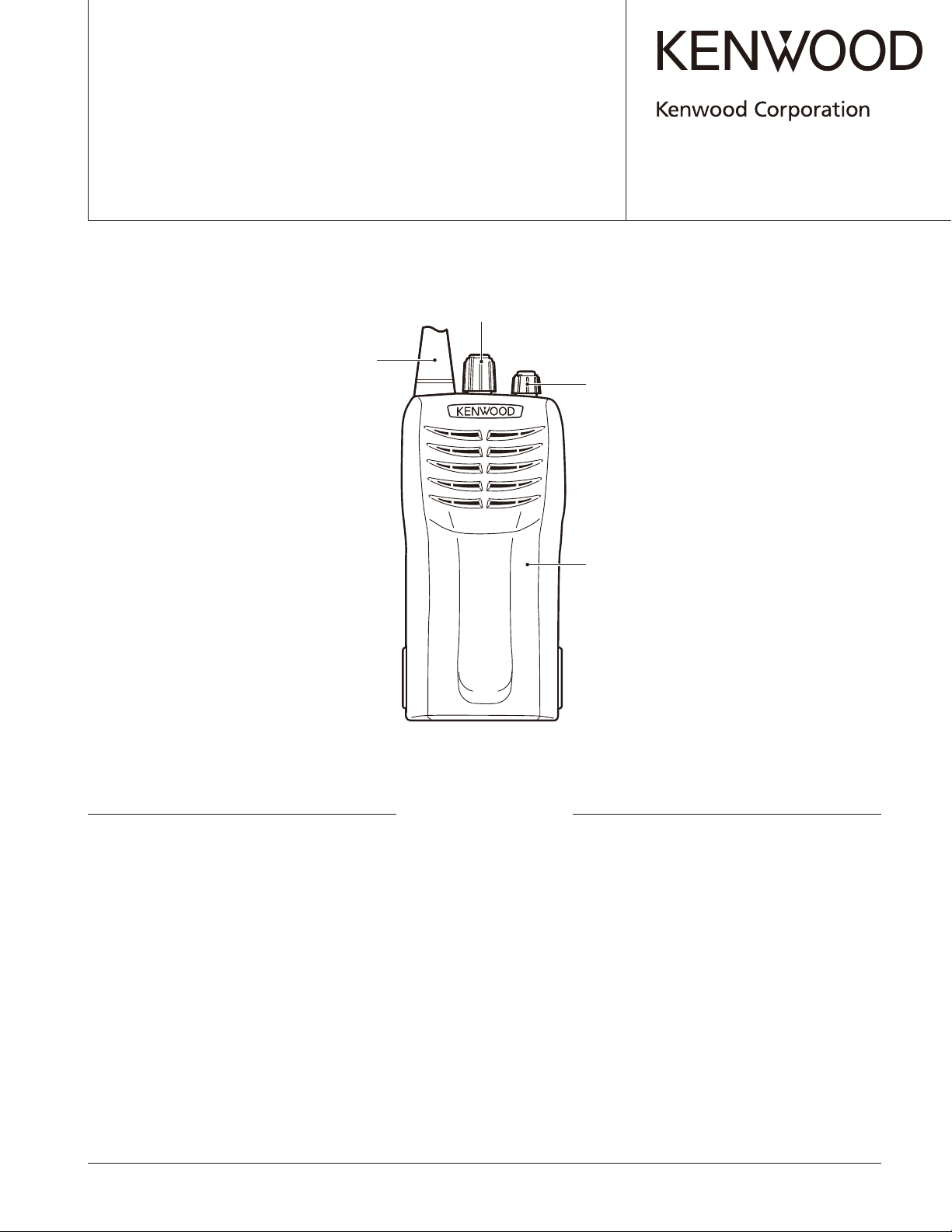
Knob (CH)
(K29-5278-03)
Helical antenna
(T90-1036-15)
© 2008-8 PRINTED IN JA PAN
B51-8841-00 (N) 554
Knob (VOL)
(K29-5255-03)
CONTENTS
GENERAL .....................................................2
SYSTEM SET-UP .........................................2
REALIGNMENT ...........................................3
DISASSEMBLY FOR REPAIR ......................5
CIRCUIT DESCRIPTION ..............................6
SEMICONDUCTOR DATA .........................10
Plastic cabinet assy
(A02-4049-03)
PC BOARD
TX-RX UNIT (X57-6020-10) .................26
SCHEMATIC DIAGRAM ............................30
BLOCK DIAGRAM .....................................34
LEVEL DIAGRAM ......................................36
OPTIONAL ACCESSORIES
COMPONENTS DESCRIPTION .................11
PARTS LIST ...............................................12
EXPLODED VIEW ......................................19
PACKING ....................................................20
ADJUSTMENT ..........................................21
KNB-14 (Ni-Cd BATTERY) ....................37
KNB-15A (Ni-Cd BATTERY) .................37
KNB-20N (Ni-MH BATTERY) ...............37
SPECIFICATIONS ...................BACK COVER
Page 2
TK-2102G
Document Copyrights
Copyright 2008 by Kenwood Corporation. All rights re-
served.
No part of this manual may be reproduced, translated,
distributed, or transmitted in any form or by any means,
electronic, mechanical, photocopying, recording, or otherwise, for any purpose without the prior written permission
of Kenwood.
GENERAL
INTRODUCTION
SCOPE OF THIS MANUAL
This manual is intended for use by experienced technicians familiar with similar types of commercial grade communications equipment. It contains all required service
information for the equipment and is current as of the publication date. Changes which may occur after publication
are covered by either Service Bulletins or Manual Revisions.
These are issued as required.
ORDERING REPLACEMENT PARTS
When ordering replacement parts or equipment information, the full part identifi cation number should be included.
This applies to all parts : components, kits, or chassis. If the
part number is not known, include the chassis or kit number
of which it is a part, and a suffi cient description of the required component for proper identifi cation.
Disclaimer
While every precaution has been taken in the preparation
of this manual, Kenwood assumes no responsibility for errors or omissions. Neither is any liability assumed for damages resulting from the use of the information contained
herein. Kenwood reserves the right to make changes to any
products herein at any time for improvement purposes.
PERSONAL SAFETY
The following precautions are recommended for personal
safety:
• DO NOT transmit until all RF connectors are verifi ed se-
cure and any open connectors are properly terminated.
• SHUT OFF and DO NOT operate this equipment near
electrical blasting caps or in an explosive atmosphere.
• This equipment should be serviced by a qualifi ed techni-
cian only.
SERVICE
This transceiver is designed for easy servicing. Refer to
the schematic diagrams, printed circuit board views, and
alignment procedures contained within.
NOTE
You must use KPG-55D version 4.00 or later for this
transceiver. KPG-55D versions earlier than version 4.00 will
not work properly.
SYSTEM SET-UP
Merchandise received
License and frequency allocated by FCC
Choose the type of transceiver
Transceiver programming
Are you using the speaker microphone?
NO
Delivery
2
Frequency range (MHz) RF power Type
TX/RX 150~174
A personal computer (IBM PC or compatible), programming
interface (KPG-22/22A), USB adapter (KCT-53U), and programming
software (KPG-55D ver.4.00 or later) are required for programming.
(The frequency, and signaling data are programmed for the transceiver.)
YES
KMC-17 or KMC-21
Speaker microphone
(Option)
5.0W
TK-2102G K,M
Page 3
REALIGNMENT
TK-2102G
1. Modes
User mode
PC mode
Mode Function
User mode For normal use.
PC mode
Data programming
mode
PC test mode
Used for communication between the transceiver and PC.
Used to read and write frequency data and
other features to and from the transceiver.
Used to check the transceiver using the PC.
This feature is included in the FPU.
Data programming mode
PC test mode PC tuning mode
2. How to Enter Each Mode
Mode Operation
User mode Power ON
PC mode Received commands from PC
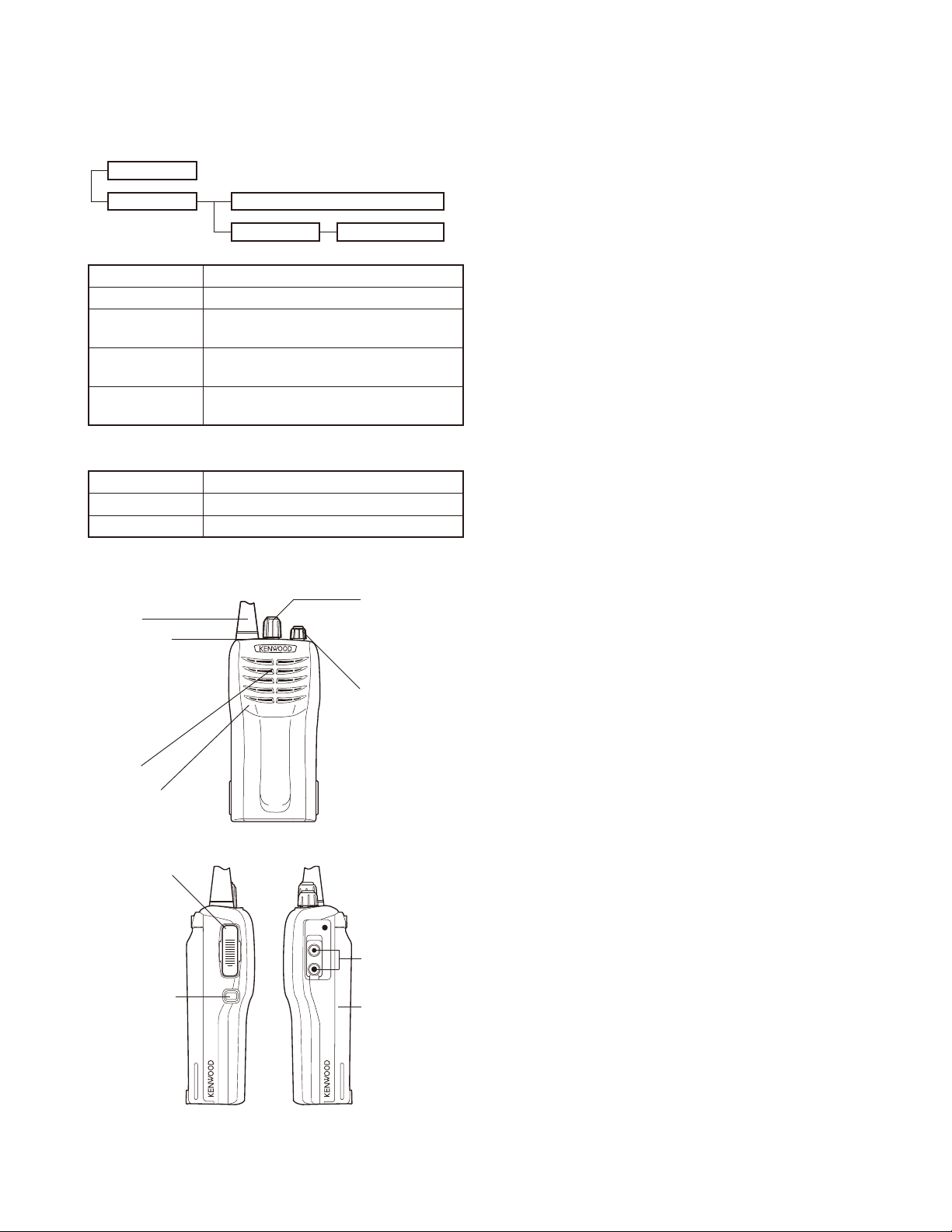
3. Getting Acquainted
Antenna
LED indicator
Lights red while
transmitting.
Lights green while
receiving a signal.
Flashes red when
the battery voltage
is low while
transmitting.
Speaker
Microphone
PTT (Push-ToTalk) switch
Press, then
speak into the
microphone to
call a station.
Release to
receive.
Monitor key
Press and hold to
turn the squelch
OFF. You will
hear background
noise. Release
to turn the
squelch back ON.
Channel
selector
Rotate to select
channels 1 ~ 16.
Power switch/
Volume control
Turn clockwise
to switch ON the
transceiver. To
switch OFF the
transceiver, turn
counterclockwise
until a click
sounds. Rotate
to adjust the
volume level.
Speaker/
microphone
jacks
Battery pack
(KNB-15A)
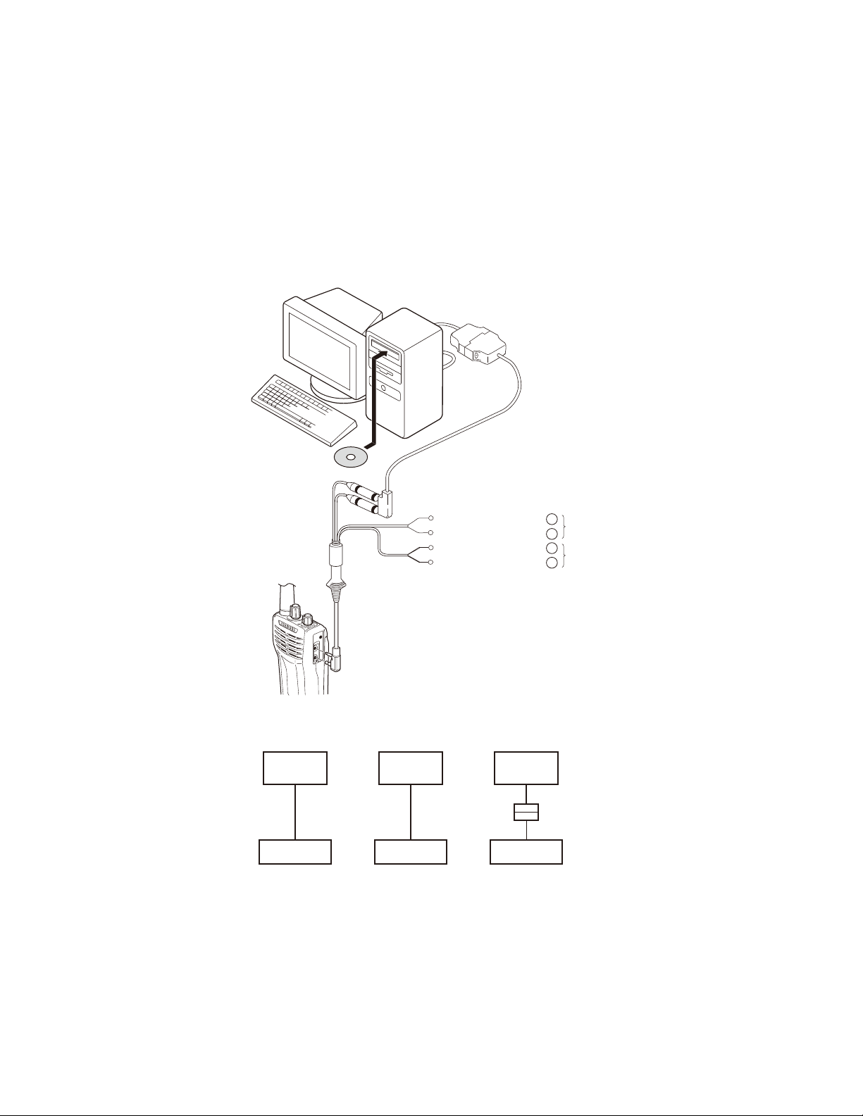
4. PC Mode
4-1. Preface
The transceiver is programmed by using a personal computer, a programming interface (KPG-22/22A), USB adapter
(KCT-53U) and programming software (KPG-55D (ver.4.00 or
later)).
The programming software can be used with a PC. Figure 1 shows the setup of a PC for programming.
4-2. Connection Procedure
1. Connect the transceiver to the personal computer with
the interface cable and USB adapter (when the interface
cable is KPG-22A, the KCT-53U can be used.).
Notes:
• You must install the KCT-53U driver in the computer to
use the USB adapter (KCT-53U).
• When using the USB adapter (KCT-53U) for the fi rst time,
plug the KCT-53U into a USB port on the computer with
the computer power ON.
2. When the POWER is switched on, user mode can be en-
tered immediately. When the PC sends a command, the
transceiver enters PC mode.
When data is transmitting from the transceiver, the red
LED lights.
When data is received by the transceiver, the green LED
lights.
Notes :
• The data stored in the personal computer must match
the Model Name when it is written into the EEPROM.
• Do not press the [PTT] key during data transmission or
reception.
• Change the transceiver to PC mode, then attach the in-
terface cable.
4-3. KPG-22/KPG-22A Description
(PC programming interface cable : Option)
The KPG-22/22A is required to interface the transceiver
with the computer. It has a circuit in its D-sub connector
(KPG-22: 25-pin, KPG-22A: 9-pin) case that converts the RS232C logic level to the TTL level.
The KPG-22/22A connects the SP/MIC connector of the
transceiver to the RS-232C serial port of the computer.
4-4. KCT-53U Description (USB adapter : Option)
The KCT-53U is a cable which connects the KPG-22A to
a USB port on a computer.
When using the KCT-53U, install the supplied CD-ROM
(with driver software) in the computer. The KCT-53U driver
runs under Windows 2000 or XP.
3
Page 4
TK-2102G
REALIGNMENT
4-5. Programming Software Description
The KPG-55D (ver.4.00 or later) is the programming
software for the transceiver supplied on a CD-ROM. This
software runs under Windows 2000, XP or Vista (32-bit) on
a PC.
KPG-55D
(ver.4.00 or later)
4-6. Programming with PC
the KPG-55D (ver.4.00 or later), the data for each set can be
modifi ed.
format via the SP/MIC jack.
PC
KPG-22 or KPG-22A or
KPG-22A+KCT-53U
Illustration is KPG-22
Gray
Gray/Black
1.5D-XV Lead wire
1.5D-XV Shield wire
If data is transferred to the transceiver from a PC with
Data can be programmed into the EEPROM in RS-232C
In this mode the PTT line operate as RXD data line.
+
SP
–
+
MIC
–
PC
D-SUB
(25-pin)
KPG-22
Transceiver
Tuning cable
(E30-3216-05)
PC
D-SUB
(9-pin)
Transceiver
Fig. 1
PC
USB
KCT-53U
KPG-22A
KPG-22A
Transceiver
4
Page 5
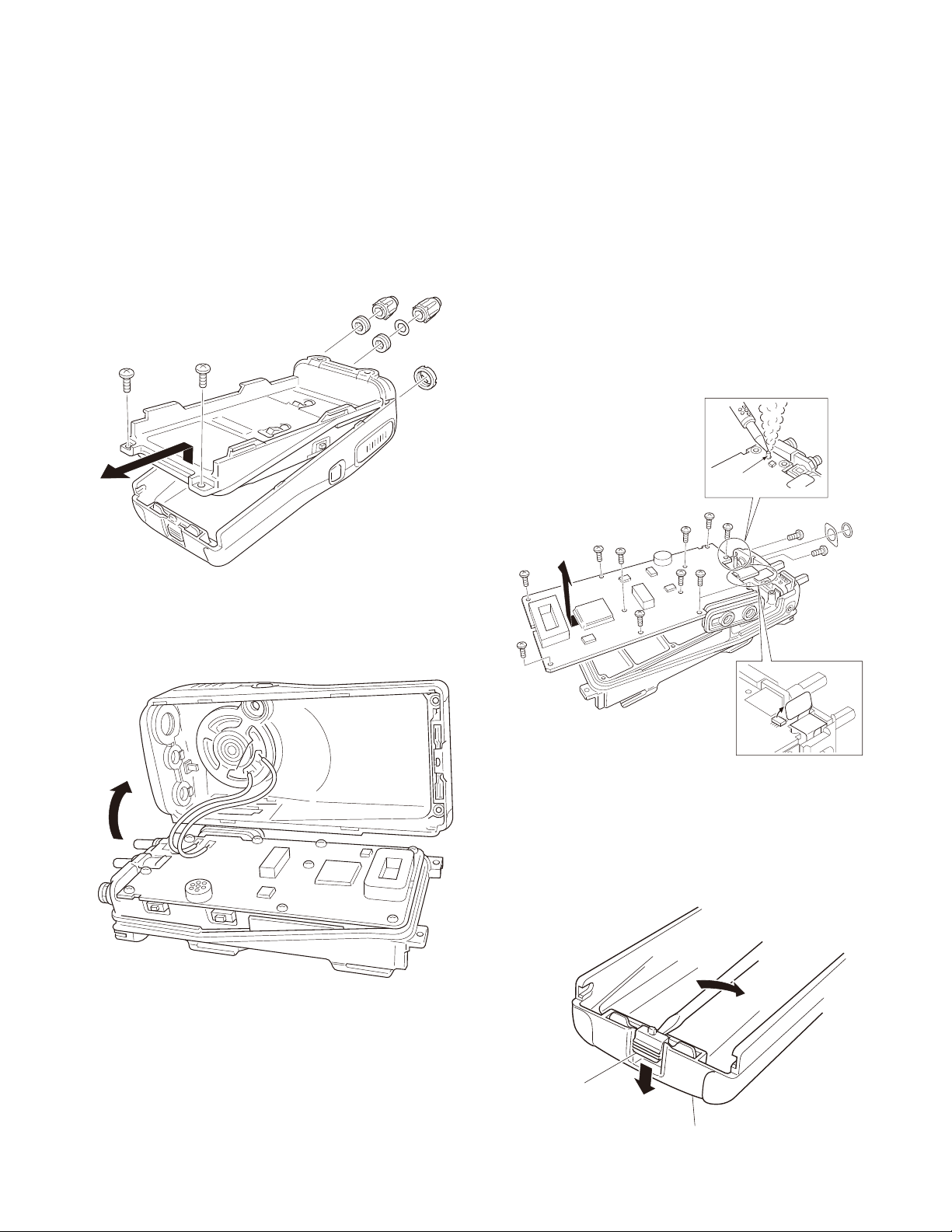
DISASSEMBLY FOR REPAIR
TK-2102G
Removing the case assembly from the chassis
■
1. Remove the two knobs q, cushion w and three round
nuts e.
2. Remove the two screws r.
3. Expand the right and left sides of the bottom of the case
assembly, then Iift and remove the chassis from the case
assembly t.
=
;
;
:
.
.
:
@
.
Removing the TX-RX unit from the chassis
■
1. Remove the eleven screws u.
2. Remove the VOL/CH FPC from the TX-RX unit connector
(CN400) i.
3. Remove the solder from the antenna terminal using a
soldering iron, then lift the unit off o.
4. Remove the waterproof packing
the antenna connector.
Note: The cushion cannot be reused. Affi x a new cush-
ion when you remove the cushion.
5. Remove the two screws
nector.
Note: When reassembling the unit in the chassis, be
sure to solder the antenna terminal.
>
>
>
and remove the antenna con-
!2
>
>
>
>
and cushion
!0
8
Antenna
terminal
>
!1
from
4. Taking care not to cut the speaker lead y, open the
chassis and case assembly.
B
>
2
CN400
Removing the lever
■
1. Press down the lever on the lower case !3, insert a small
fl at-head screwdriver into the space between the case
and lever, open the case carefully !4 and lift the lever off.
Note: Do not force to remove the lever from the case.
Lever knob
Case assembly
5
Page 6
TK-2102G
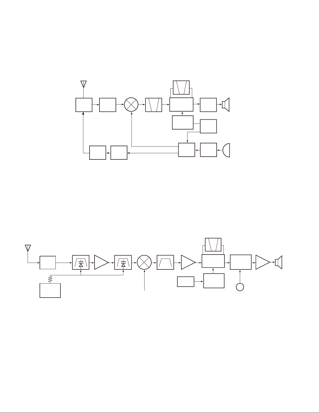
CIRCUIT DESCRIPTION
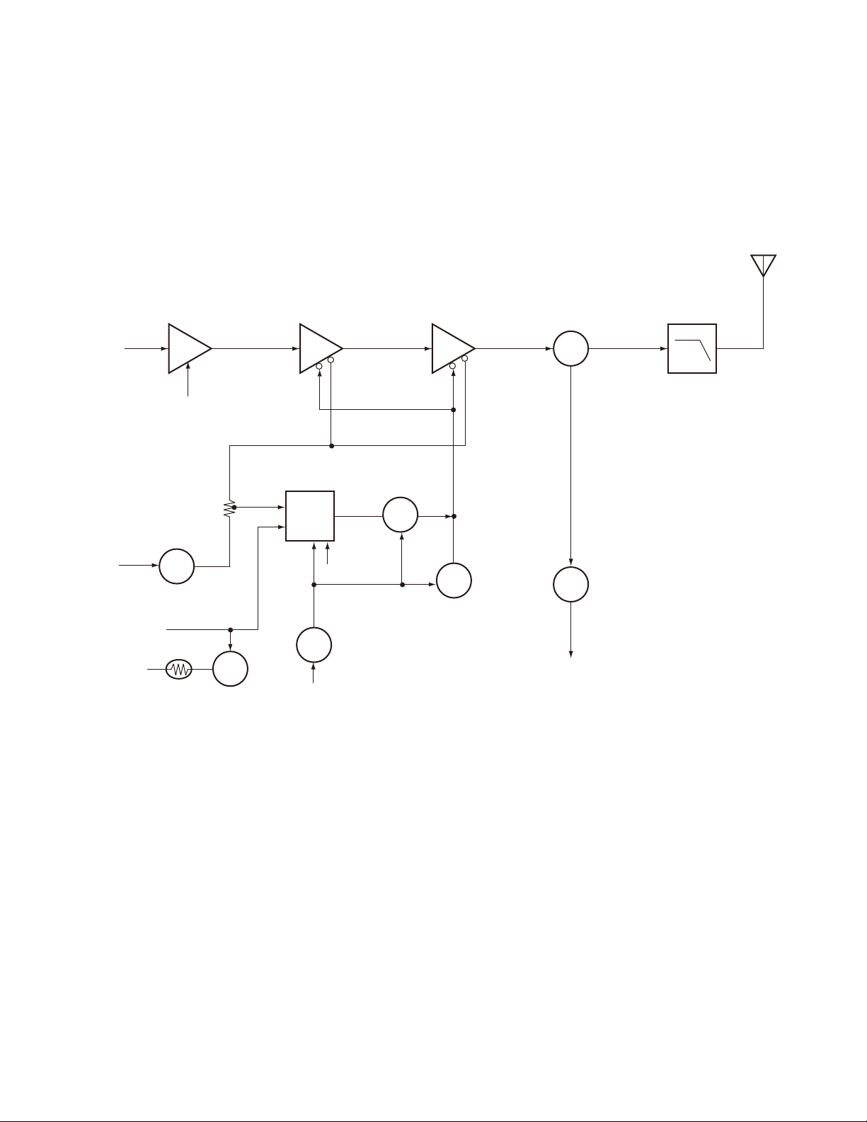
1. Frequency Confi guration
The receiver utilizes double conversion. The first IF is
38.85MHz and the second IF is 450kHz. The fi rst local oscillator signal is supplied from the PLL circuit.
ANT
PA
AMP
RF
AMP
TX
AMP
38.85MHz
RX
TX
ANT SW
Fig. 1 Frequency confi guration
2. Receiver
The receiver is double conversion superheterodyne, designed to operate in the frequency range of 150 to 174MHz.
The frequency confi guration is shown in Fig. 1.
1) Front-end RF Amplifi er
An incoming signal from the antenna is applied to an RF
amplifier (Q203) after passing through a transmit/receive
switch circuit (D102 and D103 are off) and a band pass fi lter
ANT
D102, D103
ANT SW
APC
IC403
MPU
TUNE
BPF
RF AMP
Q203
BPF
MIXER
Q202
1st Local OSC
(PLL)
The PLL circuit in the transmitter generates the neces-
sary frequencies. Fig. 1 shows the frequencies.
CF
450kHz
MCF
38.4MHz
IF SYSTEM
X3
multiply
PLL
VCO
AF
AMP
TCXO
MIC
AMP
SP
12.8MHz
MIC
(L208, L209 and L210). After the signal is amplifi ed (Q203),
the signal is filtered through a band pass filter (L203 and
L214) to eliminate unwanted signals before it is passed to
the fi rst mixer. Band pass fi lters (L208, L209, L210, L203
and L214) have varactor diodes (D203, D204, D205, D202
and D201).
The voltage of these diodes are controlled by to track the
MPU (IC403) center frequency of the band pass fi lter. (See
Fig. 2)
CF200
MCF
XF200
IF AMP
Q201
TCXO
IF, MIX, DET
IC200
X3
multiply
Q1
AF AMP
LPF, HPF
IC300
WIDE/NARROW SW
Q303
AF PA AMP
IC302
SP
Fig. 2 Receiver section confi guration
2) First Mixer
The signal from the RF amplifi er is heterodyned with the
fi rst local oscillator signal from the PLL frequency synthesizer circuit at the fi rst mixer (Q202) to create a 38.85MHz
fi rst intermediate frequency (1st IF) signal. The fi rst IF signal
is then fed through two monolithic crystal filters (MCFs :
XF200) to further remove spurious signals.
3) IF Amplifi er
The fi rst IF signal is amplifi ed by Q201, and then enters
IC200 (FM processing IC). The signal is heterodyned again
with a second local oscillator signal within IC200 to create
a 450kHz second IF signal. The second IF signal is then fed
6
through a 450kHz ceramic fi lter (CF200) to further eliminate
unwanted signals before it is amplifi ed and FM detected in
IC200.
4) AF Amplifi er
The recovered AF signal obtained from IC200 is amplifi ed
by IC300 (1/4), fi ltered by the IC300 low-pass fi lter (2/4) and
IC300 high-pass filter (3/4) and (4/4), and de-emphasized
by R303 and C306. The AF signal is then passed through a
WIDE/NARROW switch (Q303). The processed AF signal
passes through an AF volume control and is amplifi ed to a
suffi cient level to drive a loud speaker by an AF power amplifi er (IC302).
Page 7
CIRCUIT DESCRIPTION
TK-2102G
XF200:L71-0522-05
Item Rating
Nominal center frequency 38.850MHz
Pass band width ±5.0kHz or more at 3dB
40dB stop band width ±20.0kHz or less
Ripple 1.0dB or less
Insertion loss 4.0dB or less
Guaranteed attenuation 80dB or more at fo -910kHz
Terminal impedance 610Ω /3PF
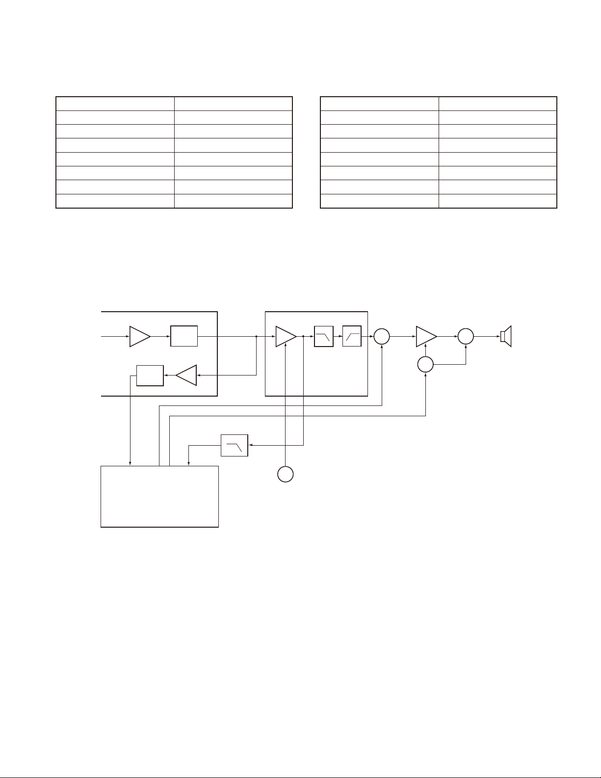
5) Squelch
Part of the AF signal from the IC enters the FM IC again,
and the noise component is amplifi ed and rectifi ed by a fi lter
and an amplifi er to produce a DC voltage corresponding to
the noise level.
The DC signal from the FM IC goes to the analog port of
IC200
FM IF IC
IF AMP DET
DET
HPF
AMP
IC300
AF AMP
CF200:L72-0958-05
Item Rating
Nominal center frequency 450kHz
6dB band width ±6.0kHz or more
50dB band width ±12.5kHz or less
Ripple 2.0dB or less at fo ±4kHz
Insertion loss 6.0dB or less
Guaranteed attenuation 35.0dB or more at fo ±100kHz
Terminal impedance 2.0 k
the microprocessor (IC403). IC403 determines whether to
output sounds from the speaker by checking whether the
input voltage is higher or lower than the preset value.
To output sounds from the speaker, IC403 sends a high
signal to the MUTE and AFCO Iines and turns IC302 on
through Q302, Q304, Q305, Q306 and Q307.(See Fig. 3)
LPF HPF
Q302
SW
IC302
AF PA AMP
Ω
Q307
SW
Q304, 305, 306
SW
SP
IC301
LPF
6
BUSY
IC403
MPU
MUTE
AFCO
56762
TI
QT/DQT
Fig. 3 AF amplifi er and squelch
6) Receive Signaling
QT/DQT
300 Hz and higher audio frequencies of the output signal
from IF IC are cut by a low-pass fi lter (IC301). The resulting
signal enters the microprocessor (IC403). IC403 determines
whether the QT or DQT matches the preset value, and controls the MUTE and AFCO and the speaker output sounds
according to the squelch results.
Q303
W/N SW
3. PLL Frequency Synthesizer
The PLL circuit generates the fi rst local oscillator signal
for reception and the RF signal for transmission.
1) PLL
The frequency step of the PLL circuit is 5 or 6.25kHz.
A 12.8MHz reference oscillator signal is divided at IC1 by
a fi xed counter to produce the 5 or 6.25kHz reference frequency. The voltage controlled oscillator (VCO) output signal
is buffer amplifi ed by Q6, then divided in IC1 by a dual-module programmable counter . The divided signal is compared
in phase with the 5 or 6.25kHz reference signal in the phase
comparator in IC1. The output signal from the phase comparator is fi ltered through a low-pass fi lter and passed to the
VCO to control the oscillator frequency. (See Fig.4)
7
Page 8
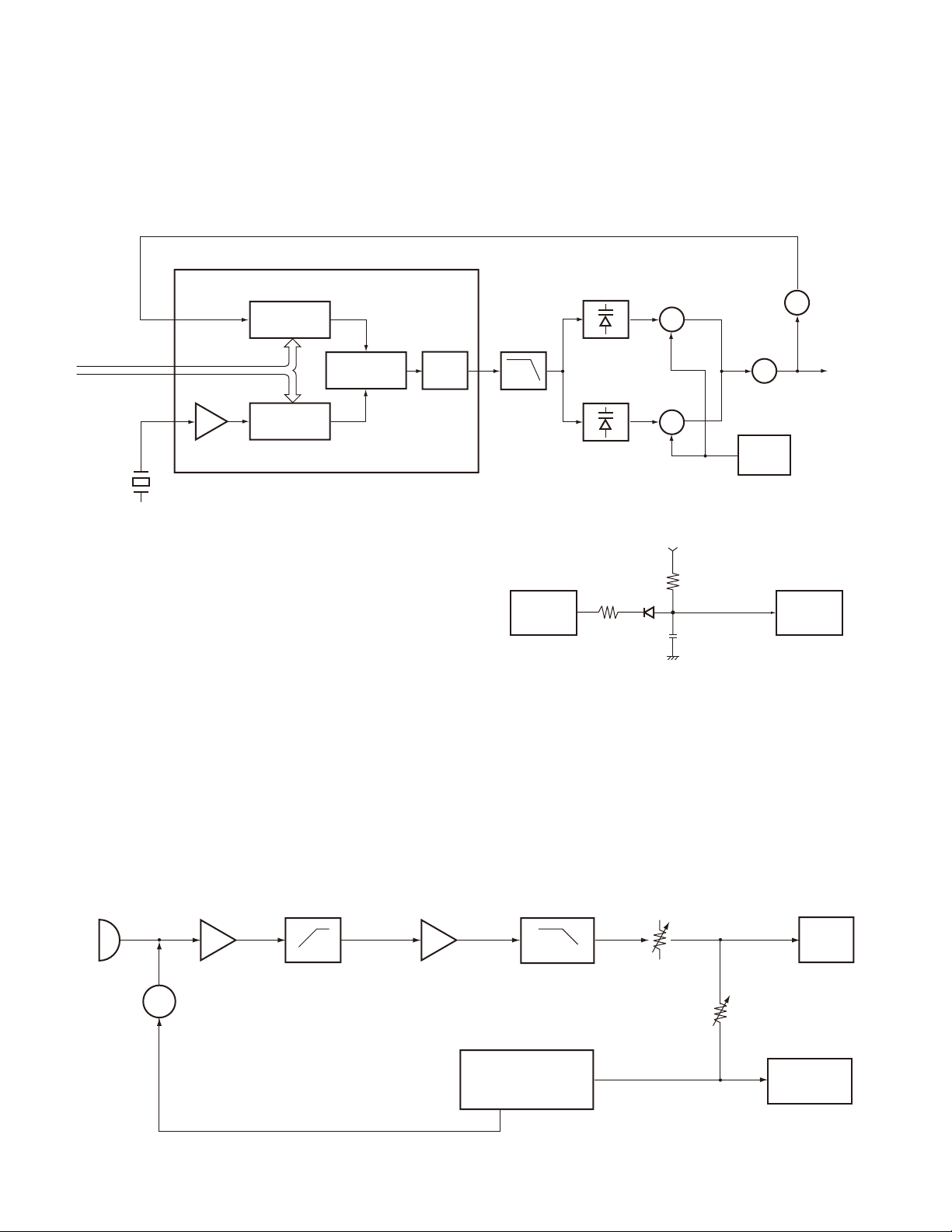
TK-2102G
CIRCUIT DESCRIPTION
2) VCO
The operating frequency is generated by Q4 in transmit
mode and Q3 in receive mode. The oscillator frequency is
controlled by applying the VCO control voltage, obtained
from the phase comparator, to the varactor diodes (D1 and
PLL IC IC1
I/N
PLL DATA
REF OSC
I/M
12.8MHz
5kHz/6.25kHz
PHASE
COMPARATOR
5kHz/6.25kHz
CHARGE
PUMP
Fig. 4 PLL circuit
3) Unlock Detector
If a pulse signal appears at the LD pin of IC1, an unlock
condition occurs, and the DC voltage obtained from D7, R1,
and C1 causes the voltage applied to the UL pin of the microprocessor to go low. When the microprocessor detects
this condition, the transmitter is disabled, ignoring the pushto-talk switch input signal. (See Fig.5)
D2 in transmit mode and D3 and D4 in receive mode). The
T/R pin is set high in receive mode causing Q5 and Q7 to
turn Q4 off, and turn Q3 on . The T/R pin is set low in transmit mode. The outputs from Q3 and Q4 are amplifi ed by Q6
and sent to the buffer amplifi ers.
D7
Q4
TX VCO
Q3
RX VCO
5C
Q2
RF AMP
Q6
BUFF AMP
Q5, 7
T/R SW
R1
C1
IC403
UL
MPU
D1, 2
LPF
D3, 4
IC1
LD
PLL IC
4. Transmitter
1) Transmit Audio
The modulation signal from the microphone is amplifi ed
by IC500 (1/2), passes through a pre-emphasis circuit, and
amplifi ed by the other IC500 (1/2) to perform IDC operation.
The signal then passes through a low-pass filter (splatter
fi Iter) (Q501 and Q502) and cuts 3kHz and higher frequencies. The resulting signal goes to the VCO through the VCO
modulation terminal for direct FM modulation. (See Fig. 6)
MIC
IC500 (1/2)
MIC
AMP
Q503
SW
PRE-EMPHASIS
IC500 (1/2)
IDC
Fig. 5 Unlock detector circuit
2) QT/DQT Encoder
A necessary signal for QT/DQT encoding is generated by
IC403 and FM-modulated to the PLL reference signal. Since
the reference OSC does not modulate the loop characteristic frequency or higher, modulation is performed at the VCO
side by adjusting the balance. (See Fig. 6)
Q501, 502
LPF
(SPLATTER FILTER)
IC403
TO
MUTE
VR501
MAX
DEV
VR500
BALANCE
QT/DQT
D5, Q4
VCO
X1, IC1
REFERENCE
OSC
(TCXO)
Fig. 6 Transmit audio and QT/DQT encoder
8
Page 9
CIRCUIT DESCRIPTION
TK-2102G
3) VCO and RF Amplifi er
The transmit signal obtained from the VCO buffer amplifi er Q100, is amplifi ed by Q101. This amplifi ed signal is
passed to the power amplifi er, Q102 and Q105, which consists of a 2-stage FET amplifi er and is capable of producing
up to 5W of RF power. (See Fig.7)
AMP
Q101
5T
DET
Q103,104
B SW
B
DRIVE AMP
Q102
APC
IC100
5T
Q109
4) ANT Switch and LPF
The RF amplifi er output signal is passed through a lowpass fi lter network and a transmit/receive switching circuit
before it is passed to the antenna terminal. The transmit/
receive switching circuit is comprised of D101, D102, D103
and D104. D102 and D103 turned on (conductive) in transmit mode and off (isolated) in receive mode.
FINAL AMP
Q105
SW
Q106
SW
ANT SW
D101,104
ANT SW
D102,103
LPF
ANT
APC
TH100
5T
SW
Q107
Q108
SW
5T
Fig. 7 APC system
5) APC
The automatic power control (APC) circuit stabilizes the
transmitter output power at a predetermined level by sensing the drain current of the fi nal amplifi er Field Effect Transistor (FET) . The voltage comparator, IC100 (2/2), compares
the voltage obtained from the above drain current with a
reference voltage which is set using the microprocessor.
An APC voltage proportional to the difference between the
sensed voltage and the reference voltage appears at the
output of IC100 (1/2). This output voltage controls the gate
of the FET power amplifier, which keeps the transmitter
output power constant. The transmitter output power can
be varied by the microprocessor which in turn changes the
reference voltage and hence, the output power.
6) Thermal Protection Circuit
When the thermistor (TH100) reaches about 80˚C, the
protection circuit turns on Q107 to protect transmitting fi nal
amplifi er (Q105) from the over heating.
RX
5. Power Supply
A 5V reference power supply [5M] for the control circuit
is derived from an internal battery. This reference is used
to provide a 5V supply in transmit mode [5T], a 5V supply in
receive mode [5R], and a 5V supply common in both modes
[5C] based on the control signal sent from the microprocessor.
6. Control System
The IC403 MPU operates at 7.37MHz . This oscillator has
a circuit that shifts the frequency according to the EEPROM
data.
9
Page 10
TK-2102G
SEMICONDUCTOR DATA
Microprocessor: 38268MCA060GU (TX-RX unit IC403)
Pin No.
11~14 NC I NC
24~27 NC I NC
28~31 ENC3~ENC0 l Encode input (channel select)
43~46 NC l NC
50~54 NC l NC
59,60 NC O NC
Port Name I/O Function
1,2 VC1,VC2 O Variable capacity tune control
3NC INC
4 TIBI I
5 TI I QT/DQT signal input
6 BUSY I Busy input
7 BATT l Battery voltage detection
8NC lNC
9 VCCN O Frequency regulation output
10 APC O
15 BEEP O Beep output
16 TO O QT/DQT output
17 NC l NC
18 PTT I [PTT] key input connected to RXD
19 TXD O
20 RXD I
21 NC l NC
22 SELF l Self program L : disable
23 MONl I [MONl] key input
32 INT0 l Power detection control
33 RST I Reset input
34 NC I NC
35 NC O NC
36 XIN l 7.3728MHz oscillator
37 XOUT O 7.3728MHz oscillator
38 VSS I GND
39 SHIFT O Beat shift H : shift on
40 PABC O Final supply H : on
41 WNRC O
42 WNTC O MAX Dev. control Narrow: H
47 SDA l/O EEPROM data line
48 SCL O EEPROM clock line
49 UL I PLL unlock detection pin L : unlock
55 DT O Common data output
56 CK O Common clock output
57 NC O NC
58 LE O PLL IC enable H : latches
QT/DQT external circuit center point
input
TX : Auto power control D/A output
RX : BPF tuning D/A output
RS-232C output connected to SP/
MIC test (REM)
RS-232C input connected to [PTT]
line
Audio reference sensitivity L : narrow
Pin No.
70~88 NC O NC
92~95 NC O NC
96~100
Port Name I/O Function
Control of power supply (5M) for
61 5MC O
62 AFCO O AF amp power suppIy H : ON
63 RX O TX/RX VCO select H : RX
64 GLED O Green LED control H : Lit
65 RLED O Red LED control H : Lit
66 SAVE O Save control H : Save off
67 MUTE O
68 5RC O
69 5TC O
89 VCC l
90 VREF l
91 AVSS l
NC I NC
everything except the
microprocessor and EEPROM
L : Power supply ON
Mute control
H : MIC mute, L : AF mute
Reception power suppIy control
L : on
Transmission power suppIy control
H : on
Microprocessor power supply, 5V input
A/D conversion reference voltage ;
connected to Vcc
A/D converter power supply ; connected to Vss
FET : 2SK2596-E (Q102)
Absolute Maximum Ratings (Ta=25°C)
Item V
Rating 17V ±10V 0.4A 3W 150°C -45~+150°C
DSSVGSS
I
Pch* Tch Tstg
D
*Tc=25°C
FET : 2SK2595-E (Q105)
Absolute Maximum Ratings (Ta=25°C)
Item V
Rating 17V ±10V 1.1A 20W 150°C -45~+150°C
DSSVGSS
I
Pch* Tch Tstg
D
*Tc=25°C
10
Page 11
COMPONENTS DESCRIPTION
TX-RX unit (X57-6020-10)
Ref. No. Part Name Description
IC1 IC Phase locked loop system
IC100 IC Automatic power control
IC200 IC IF system
IC300 IC Audio amp active fi lter
IC301 IC Active fi lter
IC302 IC Audio power AMP
IC400 IC Reset switch
IC401 IC EEPROM
IC402 IC Voltage detect
IC403 IC Microprocessor
IC404 IC Voltage regulator
IC500 IC MIC AMP/Limiter
Q1 Transistor Tripler
Q2 Transistor RF AMP
Q3 FET VCO RX
Q4 FET VCO TX
Q5 FET DC switch
Q6 Transistor RF buffer AMP
Q7 Transistor DC switch
Q8 Transistor Ripple fi lter
Q100 Transistor RF AMP
Q101 Transistor TX pre-drive
Q102 FET TX drive
Q103 FET DC switch
Q104 Transistor DC switch
Q105 FET TX fi nal
Q106 FET DC switch
Q107 Transistor
Q108,109 Transistor DC switch
Q200 Transistor DC switch
Q201 Transistor IF AMP
Q202 FET Mixer
Q203 FET Mixer RF AMP
Q300 Transistor Active fi lter
Q302 FET Audio mute switch
Q303~306 Transistor DC switch
Q307 FET Audio mute switch
Q400~402 Transistor DC switch
Q403 Transistor Beat shift switch
Q404 Transistor DC switch
Q405 FET DC switch
Q406~408 Transistor DC switch
Q500 FET DC switch
Q501,502 Transistor Active fi lter
Temperature protection
switch
TK-2102G
Ref. No. Part Name Description
Q503 Transistor MIC mute/ AGC
Q504 Transistor DC switch
D1~4
D5
D6 Diode Current steering
D7 Diode Unlock detect
D100 Diode RF switch
D101~104 Diode Antenna switch
D200 Diode RF switch
D201~205
D300 Diode Limiter
D400 LED TX
D401 LED Busy
D500 Diode AGC detect
D501 Diode MIC mute/AGC switch
D502 Diode Reverse protection
D505 Zener diode APC voltage limiter
Variable capacitance
diode
Variable capacitance
diode
Variable capacitance
diode
Frequency control
TX modulation
BPF tuning
11
Page 12
TK-2102G
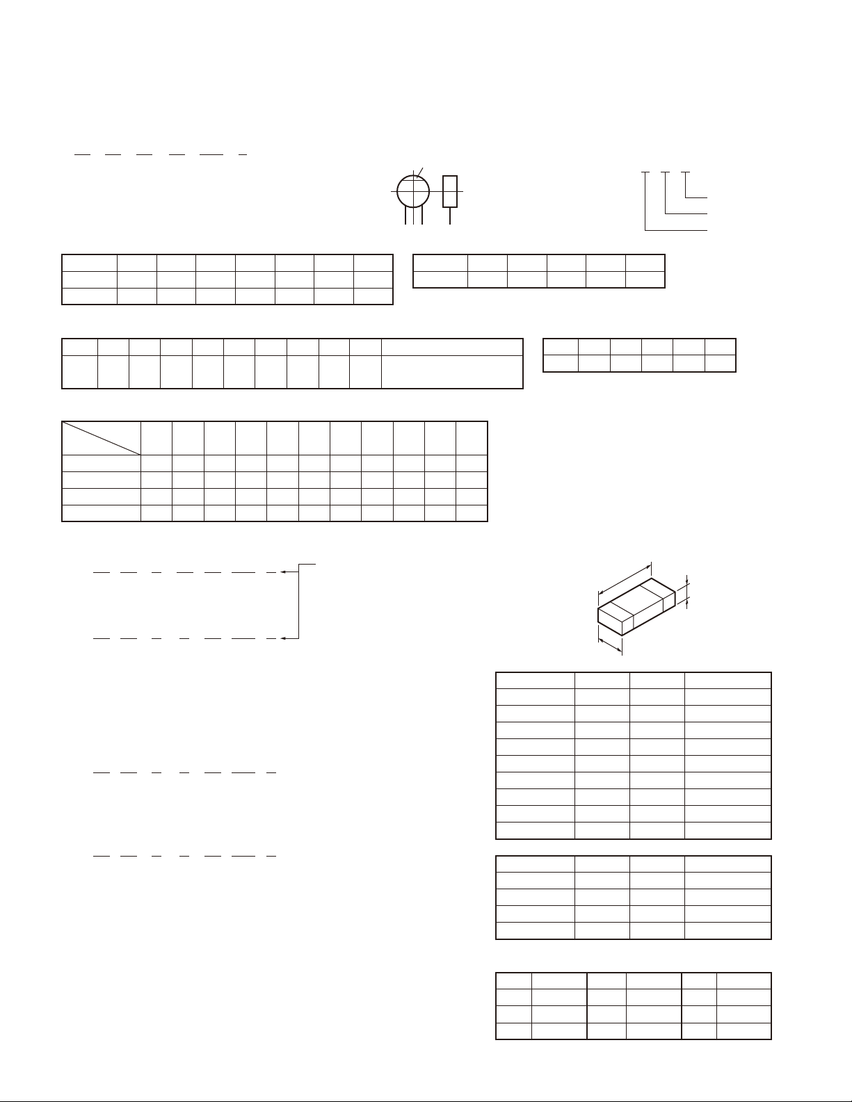
#!0!#)4/23
C C 4 5 T H 1 H 2 2 0 J
1 2 3 4 5 6
1 = Type ... ceramic, electrolytic, etc. 4 = Voltage rating
2 = Shape ... round, square, etc. 5 = Value
3 = Temp. coefficient 6 = Tolerance
s4EMPERATURECOEFFICIENT
1st Word C L P R S T U
Color* Black Red Orange Yellow Green Blue Violet
ppm/°C 0 –80 –150 –220 –330 –470 –750
PARTS LIST
CC45
Color*
2nd Word G H J K L
ppm/°C ±30 ±60 ±120 ±250 ±500
Example : CC45TH = –470±60ppm/°C
s#APACITORVALUE
010 = 1pF 2 2 0 = 22pF
100 = 10pF
101 = 100pF Multiplier
102 = 1000pF = 0.001μF 2nd number
103 = 0.01μF 1st number
s4OLERANCE-ORETHANP&
Code C D G J K M X Z P No code
(%) ±0.25 ±0.5 ±2 ±5 ±10 ±20 +40 +80 +100 More than 10μF : –10~+50
–20 –20 –0 Less than 4.7μF : –10~+75
s6OLTAGERATING
2nd word
A B C D E F G H J K V
1st word
0 1.0 1.25 1.6 2.0 2.5 3.15 4.0 5.0 6.3 8.0 –
1 10 12.5 16 20 25 31.5 40 50 63 80 35
2 100 125 160 200 250 315 400 500 630 800 –
3 1000 1250 1600 2000 2500 2150 4000 5000 6300 8000 –
s#HIPCAPACITORS
(EX) C C 7 3 F S L 1 H 0 0 0 J Refer to the table above.
1 2 3 4 5 6 7 1 = Type
(Chip) (CH, RH, UJ, SL) 2 = Shape
3 = Dimension
(EX) C K 7 3 F F 1 H 0 0 0 Z 4 = Temp. coefficient
1 2 3 4 5 6 7 5 = Voltage rating
(Chip) (B, F) 6 = Value
7 = Tolerance
2%3)34/23
s#HIPRESISTOR#ARBON
(EX) R D 7 3 E B 2 B 0 0 0 J
1 2 3 4 5 6 7
(Chip) (B, F)
s#ARBONRESISTOR.ORMALTYPE
(EX) R D 1 4 B B 2 C 0 0 0 J
1 2 3 4 5 6 7
1 = Type 5 = Rating wattage
2 = Shape 6 = Value
3 = Dimension 7 = Tolerance
4 = Temp. coefficient
s$IMENSION
Chip capacitor
Code L W T
Empty 5.6±0.5 5.0±0.5 Less than 2.0
A 4.5±0.5 3.2±0.4 Less than 2.0
B 4.5±0.5 2.0±0.3 Less than 2.0
C 4.5±0.5 1.25±0.2 Less than 1.25
D 3.2±0.4 2.5±0.3 Less than 1.5
E 3.2±0.2 1.6±0.2 Less than 1.25
F 2.0±0.3 1.25±0.2 Less than 1.25
G 1.6±0.2 0.8±0.2 Less than 1.0
H 1.0±0.05 0.5±0.05 0.5±0.05
Chip resistor
Code L W T
E 3.2±0.2 1.6±0.2 1.0
F 2.0±0.3 1.25±0.2 1.0
G 1.6±0.2 0.8±0.2 0.5±0.1
H 1.0±0.05 0.5±0.05 0.35±0.05
s2ATINGWATTAGE
Code Wattage Code Wattage Code Wattage
1J 1/16W 2C 1/6W 3A 1W
2A 1/10W 2E 1/4W 3D 2W
2B 1/8W 2H 1/2W
,ESSTHANP&
Code B C D F G
(pF) ±0.1 ±0.25 ±0.5 ±1 ±2
L
T
W
12
Page 13
PARTS LIST
TK-2102G
New Parts.
✽
Parts without Parts No. are not supplied.
Les articles non mentionnes dans le Parts No. ne sont pas fournis.
Teile ohne Parts No. werden nicht geliefert.
Ref. No.
indicates safety critical components.
New
Ad dress
Parts No. Description
parts
TK-2102G
1 1A ✽ A02-4049-03 PLASTIC CABINET ASSY
2 3B A82-0034-03 REAR PANEL
4 2D B09-0351-03 CAP (SP/MIC) ACCESSORY
5 1D ✽ B62-2103-00 INSTRUCTION MANUAL
7 2B E04-0449-05 RF COAXIAL RECEPTACLE(SMA)
8 3B E23-1183-04 RELAY TERMINAL (BATT-)
9 1A G01-0881-04 COIL SPRING (BATT RELEASE)
10 3B G10-1288-04 FIBROUS SHEET (CHASSIS)
11 - G11-2583-04 SHEET (HOLDER)
12 3B ✽ G11-2588-14 RUBBER SHEET (CHASSIS)
13 1B ✽ G11-4478-04 SHEET (CH)
15 3B G13-1709-04 CUSHION(VOL)
16 3B G13-1763-04 CUSHION (TERMINAL BATT+)
17 3B G13-1867-14 CUSHION (TERMINAL BATT-)
18 2B G13-1959-04 CUSHION (RECEPTACLE)
19 2A G13-1985-04 CUSHION (X400)
21 2B G13-1986-04 CUSHION (VR501)
22 3B G13-2069-24 CUSHION (HOLDER)
23 2B G53-0791-03 PACKING (SP/MIC)
24 2A G53-0842-13 PACKING (SP)
25 2B G53-0860-04 PACKING (CHASSIS)
Destination
L : Scandinavia K : USA P : Canada
Y : PX (Far East, Hawaii) T : England E : Eu rope
Y : AAFES (Europe) X : Australia M : Oth er Areas
TK-2102G (Y50-6410-XX)
TX-RX UNIT (X57-6020-10)
Ad dress
New
Parts No. Description
parts
Ref. No.
59 1C ✽ W08-0598-15 CHARGER ACCESSORY
60 2C W09-0940-25 BATTERY ASSY ACCESSORY
TX-RX UNIT (X57-6020-10)
D400 B30-2156-05 LED (RED)
D401 B30-2157-05 LED (YELLOW)
C1 CK73GB1C104K CHIP C 0.10UF K
C2,3 CC73GCH1H101J CHIP C 100PF J
C4 CK73GB1C104K CHIP C 0.10UF K
C5 CS77AA0J4R7M CHIP TNTL 4.7UF 6.3WV
C6 CC73GCH1H101J CHIP C 100PF J
C7 CK73GB1H102K CHIP C 1000PF K
C8 CK73FB1C224K CHIP C 0.22UF K
C9 CC73GCH1H130J CHIP C 13PF J
C10 CC73GCH1H470J CHIP C 47PF J
C12 CK73FB1C224K CHIP C 0.22UF K
C14 CC73GCH1H130J CHIP C 13PF J
C15 CS77AA1A6R8M CHIP TNTL 6.8UF 10WV
C16 CC73GCH1H680J CHIP C 68PF J
C17 CK73GB1H331K CHIP C 330PF K
C18 CS77AA1DR68M CHIP TNTL 0.68UF 20WV
Destination
27 2B G53-1528-04 PACKING (SMA)
30 1D H25-0085-04 PROTECTION BAG (100/200/0.07)
31 2D H25-2012-04 PROTECTION BAG (75/100/0.08)
33 1A J19-1572-04 HOLDER (BATT RELEASE)
34 2B J19-5344-13 HOLDER (VOL/CH)
35 2D J21-4493-04 SP/MIC HOLDER ACCESSORY
36 2D J29-0734-05 BELT CLIP ACCESSORY
37 1B J69-0345-04 RING (VOL,CH)
39 2B J82-0059-15 FPC
41 1B K29-5255-03 KNOB (VOL)
42 1A K29-5274-03 BUTTON KNOB (MONI)
43 1A K29-5275-23 BUTTON KNOB (PTT)
44 1B K29-5278-03 KNOB (CH)
45 1A K29-5337-03 LEVER KNOB (BATT RELEASE)
A 2B N09-2438-05 BINDING HEAD SCREW (SMA)
B 1B ✽ N14-0581-44 CIRCULAR NUT (VOL,CH)
C 1B ✽ N14-0804-24 CIRCULAR NUT (SMA)
D 3A N30-2606-48 PAN HEAD MACHINE SCREW
E 3B N79-2030-48 PAN HEAD TAPTITE SCREW
F 2A,2B N83-2005-48 PAN HEAD TAPTITE SCREW
47 2D N99-0396-15 SCREW SET ACCESSORY
49 2B R31-0647-05 VARIABLE RESISTOR
51 2B S60-0424-25 ROTARY SWITCH
53 1A T07-0369-15 SPEAKER
54 2D T90-1036-15 HELICAL ANTENNA ACCESSORY
56 1C ✽ W08-0479-25 AC ADAPTER (AC 120V) ACCESSORY K
58 1C W08-0558-35 AC ADAPTER (AC 230V) ACCESSORY M
C19,20 CK73GB1H103K CHIP C 0.010UF K
C23 CS77AA0J100M CHIP TNTL 10UF 6.3WV
C24 CK73GB1H681K CHIP C 680PF K
C25 CK73GB1H471K CHIP C 470PF K
C26 CC73GCH1H121J CHIP C 120PF J
C27 CK73GB1H102K CHIP C 1000PF K
C28 CC73GCH1H330J CHIP C 33PF J
C29-31 CK73GB1H102K CHIP C 1000PF K
C32 CC73GCH1H101J CHIP C 100PF J
C33 CC73GCH1H390J CHIP C 39PF J
C34 CC73GCH1HR75B CHIP C 0.75PF B
C35 CC73GCH1H060D CHIP C 6.0PF D
C36 CC73GCH1H180J CHIP C 18PF J
C37 CC73GCH1H050B CHIP C 5.0PF B
C38 CC73GCH1H180J CHIP C 18PF J
C39 CK73GB1H103K CHIP C 0.010UF K
C40,41 CK73GB1H102K CHIP C 1000PF K
C42 CK73GB1H103K CHIP C 0.010UF K
C43,44 CC73GCH1H0R5B CHIP C 0.5PF B
C45,46 CK73GB1H102K CHIP C 1000PF K
C47 CC73GCH1H330J CHIP C 33PF J
C48 CC73GCH1H100D CHIP C 10PF D
C49 CK73GB1H102K CHIP C 1000PF K
C50 CS77AA0J4R7M CHIP TNTL 4.7UF 6.3WV
C51 CC73GCH1H680J CHIP C 68PF J
C100 CC73GCH1H150J CHIP C 15PF J
C101,102 CK73GB1H102K CHIP C 1000PF K
C103 CC73GCH1H220J CHIP C 22PF J
C104-107 CK73GB1H102K CHIP C 1000PF K
C108 CC73GCH1H120J CHIP C 12PF J
C109 CK73GB1H102K CHIP C 1000PF K
13
Page 14

TK-2102G
TX-RX UNIT (X57-6020-10)
Ad dress
New
Parts No. Description
parts
Ref. No.
C110 CK73GB1C104K CHIP C 0.10UF K
C111,112 CK73GB1H102K CHIP C 1000PF K
C113 CC73GCH1H200J CHIP C 20PF J
C114-116 CK73GB1H102K CHIP C 1000PF K
C118-120 CK73GB1H102K CHIP C 1000PF K
PARTS LIST
Destination
Ref. No.
Ad dress
C241 CC73GCH1H040B CHIP C 4.0PF B
C243 CC73GCH1H020C CHIP C 2.0PF C
C245,246 CK73GB1H102K CHIP C 1000PF K
C247 CC73GCH1H200J CHIP C 20PF J
C248 CC73GCH1H080D CHIP C 8.0PF D
New
Parts No. Description
parts
Destination
C121 CK73EB1C105K CHIP C 1.0UF K
C123 CK73GB1H103K CHIP C 0.010UF K
C124 CK73GB1H102K CHIP C 1000PF K
C125 CK73GB1C104K CHIP C 0.10UF K
C126 CC73GCH1H560J CHIP C 56PF J
C127 CS77AA1A6R8M CHIP TNTL 6.8UF 10WV
C128 CC73GCH1H150G CHIP C 15PF G
C129 CC73GCH1H100C CHIP C 10PF C
C130,131 CK73GB1H102K CHIP C 1000PF K
C132 CK73GB1H471K CHIP C 470PF K
C133 CK73GB1H102K CHIP C 1000PF K
C134 CC73GCH1H101J CHIP C 100PF J
C135 CC73GCH1H270J CHIP C 27PF J
C136 CC73GCH1H390J CHIP C 39PF J
C137 CK73GB1H102K CHIP C 1000PF K
C138 CC73GCH1H100D CHIP C 10PF D
C139 CK73GB1H102K CHIP C 1000PF K
C140 CC73GCH1H100D CHIP C 10PF D
C141 CK73GB1H471K CHIP C 470PF K
C142 CC73GCH1H220J CHIP C 22PF J
C143 CC73GCH1H080D CHIP C 8.0PF D
C144 CC73GCH1H090D CHIP C 9.0PF D
C146 CC73GCH1H200J CHIP C 20PF J
C147 CC73GCH1H100D CHIP C 10PF D
C200 CS77AA0J100M CHIP TNTL 10UF 6.3WV
C201 CK73GB1H103K CHIP C 0.010UF K
C202 CC73GCH1H270J CHIP C 27PF J
C203 CK73GB1H471K CHIP C 470PF K
C204 CK73GB1H472K CHIP C 4700PF K
C205,206 CC73GCH1H391J CHIP C 390PF J
C249-251 CK73GB1H102K CHIP C 1000PF K
C252 CC73HCH1H180J CHIP C 18PF J
C253 CK73HB1H102K CHIP C 1000PF K
C254 CC73GCH1H1R5C CHIP C 1.5PF C
C255 CC73GCH1H160J CHIP C 16PF J
C256 CK73GB1H102K CHIP C 1000PF K
C257 CC73GCH1H1R5C CHIP C 1.5PF C
C259 CC73GCH1H200J CHIP C 20PF J
C260 CK73GB1H102K CHIP C 1000PF K
C261 CC73GCH1H150J CHIP C 15PF J
C262-264 CK73HB1H102K CHIP C 1000PF K
C266 CK73HB1A104K CHIP C 0.10UF K
C267 CK73GB1C104K CHIP C 0.10UF K
C300 CK73GB1H822K CHIP C 8200PF K
C301 CK73GB1E183K CHIP C 0.018UF K
C302,303 CK73GB1C104K CHIP C 0.10UF K
C304 CS77AA0J100M CHIP TNTL 10UF 6.3WV
C305 CK73GB1H103J CHIP C 0.010UF J
C306 CK73GB1C473K CHIP C 0.047UF K
C307 CS77AA0J100M CHIP TNTL 10UF 6.3WV
C308 CK73GB1H562K CHIP C 5600PF K
C309 CK73GB1H103J CHIP C 0.010UF J
C311 CS77AA0J100M CHIP TNTL 10UF 6.3WV
C312 CK73GB1H103J CHIP C 0.010UF J
C313 CK73FB1A105K CHIP C 1.0UF K
C314 CK73GB1H102K CHIP C 1000PF K
C316 CK73GB1H103J CHIP C 0.010UF J
C318 CK73GB1C333K CHIP C 0.033UF K
C319 CK73GB1C473K CHIP C 0.047UF K
C320,321 CK73GB1C333J CHIP C 0.033UF J
C207 CK73GB1C104K CHIP C 0.10UF K
C208 CC73GCH1H270J CHIP C 27PF J
C209 CK73GB1C104K CHIP C 0.10UF K
C210 CK73GB1H103K CHIP C 0.010UF K
C211 CK73GB1C104K CHIP C 0.10UF K
C212 CC73GCH1H150J CHIP C 15PF J
C213 CK73GB1C104K CHIP C 0.10UF K
C214 CK73GB1H103K CHIP C 0.010UF K
C215 CC73GCH1H100D CHIP C 10PF D
C216 CC73GCH1H020C CHIP C 2.0PF C
C217 CK73GB1H103K CHIP C 0.010UF K
C218 CK73GB1H102K CHIP C 1000PF K
C219 CC73GCH1H100C CHIP C 10PF C
C220 CK73HB1H102K CHIP C 1000PF K
C221 CK73GB1H103K CHIP C 0.010UF K
C222 CC73HCH1H050B CHIP C 5.0PF B
C223 CC73GCH1H020C CHIP C 2.0PF C
C224,225 CK73GB1C104K CHIP C 0.10UF K
C233 CC73HCH1H080B CHIP C 8.0PF B
C234 CC73HCH1H300J CHIP C 30PF J
C235 CK73GB1C104K CHIP C 0.10UF K
C236 CK73HB1H102K CHIP C 1000PF K
C237 CC73GCH1H060B CHIP C 6.0PF B
C238 CC73GCH1H200J CHIP C 20PF J
C239 CK73GB1H102K CHIP C 1000PF K
14
C322 CK73FB1E104K CHIP C 0.10UF K
C327 CK73GB1C104K CHIP C 0.10UF K
C330 CC73GCH1H101J CHIP C 100PF J
C331 CK73FB1C474K CHIP C 0.47UF K
C332 CS77AA0J100M CHIP TNTL 10UF 6.3WV
C333 CK73GB1A474K CHIP C 0.47UF K
C334 CC73GCH1H221J CHIP C 220PF J
C335 CK73GB1C473K CHIP C 0.047UF K
C336 CK73GB1H103K CHIP C 0.010UF K
C337 CS77CC0J101M CHIP TNTL 100UF 6.3WV
C338 CC73GCH1H560J CHIP C 56PF J
C400 CK73GB1C104K CHIP C 0.10UF K
C402-404 CK73GB1H102K CHIP C 1000PF K
C406,407 CK73GB1H102K CHIP C 1000PF K
C408 CS77AA0J100M CHIP TNTL 10UF 6.3WV
C409 CC73GCH1H030C CHIP C 3.0PF C
C410 CK73GB1H102K CHIP C 1000PF K
C411 CK73GB1H471K CHIP C 470PF K
C412 CC73GCH1H100D CHIP C 10PF D
C413,414 CK73GB1H102K CHIP C 1000PF K
C415 CC73GCH1H100D CHIP C 10PF D
C416 CK73GB1H102K CHIP C 1000PF K
C417 CK73EF1C105Z CHIP C 1.0UF Z
C418 CK73GB1H103K CHIP C 0.010UF K
C420,421 CK73GB1H103K CHIP C 0.010UF K
Page 15

Ref. No.
C422 CK73HB1E103K CHIP C 0.010UF K
C423 CK73GB1H102K CHIP C 1000PF K
C424 CK73FB1A105K CHIP C 1.0UF K
C425 CK73HB1E103K CHIP C 0.010UF K
C427 CK73GB1H102K CHIP C 1000PF K
Ad dress
New
Parts No. Description
parts
PARTS LIST
Destination
Ref. No.
L8,9 L40-6891-86 SMALL FIXED INDUCTOR (6.8UH)
L10 L33-0744-05 SMALL FIXED INDUCTOR
L11 L33-0745-05 SMALL FIXED INDUCTOR
L12 L40-1085-92 SMALL FIXED INDUCTOR (100NH)
L13 L40-4775-92 SMALL FIXED INDUCTOR (47NH)
Ad dress
TK-2102G
New
Parts No. Description
parts
TX-RX UNIT (X57-6020-10)
Destination
C429,430 CK73FB1A105K CHIP C 1.0UF K
C500,501 CK73GB1C273K CHIP C 0.027UF K
C502 CK73GB1H392K CHIP C 3900PF K
C503 CK73GB1C333K CHIP C 0.033UF K
C504 CS77AA0J4R7M CHIP TNTL 4.7UF 6.3WV
C505 CK73FB1A105K CHIP C 1.0UF K
C506 CK73GB1H471K CHIP C 470PF K
C507 CS77CP0G2R2M CHIP TNTL 2.2UF 4WV
C508 CK73GB1H103K CHIP C 0.010UF K
C509 CK73GB1H332K CHIP C 3300PF K
C510 CC73GCH1E821J CHIP C 820PF J
C511 CK73GB1C473K CHIP C 0.047UF K
C512 CK73GB1H332K CHIP C 3300PF K
C513 CC73GCH1E681J CHIP C 680PF J
C514 CK73GB1C473K CHIP C 0.047UF K
C515 CK73GB1H103K CHIP C 0.010UF K
C516 CC73GCH1H100D CHIP C 10PF D
C517 CK73GB1H102K CHIP C 1000PF K
C518 CK73GB1E223J CHIP C 0.022UF J
C519 CS77AA0J4R7M CHIP TNTL 4.7UF 6.3WV
C520 CK73GB1E223J CHIP C 0.022UF J
C521 CK73GB1H102K CHIP C 1000PF K
C522 CK73FB1E104K CHIP C 0.10UF K
C523 CS77CP0G2R2M CHIP TNTL 2.2UF 4WV
C524 CK73GB1C273K CHIP C 0.027UF K
C525 CK73GB1C104K CHIP C 0.10UF K
C526 CK73GB1H471K CHIP C 470PF K
C527 CS77AA0J100M CHIP TNTL 10UF 6.3WV
C528 CK73GB1H102K CHIP C 1000PF K
C529 CK73FB1H102K CHIP C 1000PF K
L14 L92-0140-05 CHIP FERRITE
L15 L40-6891-86 SMALL FIXED INDUCTOR (6.8UH)
L16,17 L40-2285-38 SMALL FIXED INDUCTOR (220NH)
L100 L40-8275-92 SMALL FIXED INDUCTOR (82NH)
L101 L40-6875-92 SMALL FIXED INDUCTOR (68NH)
L102 L92-0140-05 CHIP FERRITE
L103 L40-2775-92 SMALL FIXED INDUCTOR (27NH)
L104 L41-1098-40 SMALL FIXED INDUCTOR (1000NH)
L105 L92-0149-05 CHIP FERRITE
L107 L40-3375-54 SMALL FIXED INDUCTOR (33NH)
L108 L34-4548-05 AIR-CORE COIL
L109 L92-0149-05 CHIP FERRITE
L110 L34-4594-05 AIR-CORE COIL
L111 L34-4547-05 AIR-CORE COIL
L112 L41-2295-39 SMALL FIXED INDUCTOR (2.2UH)
L113 L34-4550-05 AIR-CORE COIL
L114 L34-4548-05 AIR-CORE COIL
L115 L34-4549-05 AIR-CORE COIL
L117 L34-4548-05 AIR-CORE COIL
L118 L41-1092-44 SMALL FIXED INDUCTOR (1UH)
L200 L41-5685-39 SMALL FIXED INDUCTOR (0.56UH)
L201 L41-8285-39 SMALL FIXED INDUCTOR (0.82UH)
L202 ✽ L40-1285-38 SMALL FIXED INDUCTOR (120NH)
L203 L41-5678-03 SMALL FIXED INDUCTOR (56NH)
L204 ✽ L41-7588-40 SMALL FIXED INDUCTOR (750NH)
L208,209 L41-5678-03 SMALL FIXED INDUCTOR (56NH)
L210 ✽ L41-4778-03 SMALL FIXED INDUCTOR (47NH)
L211 L40-3375-92 SMALL FIXED INDUCTOR (33NH)
L212 L34-4554-05 COIL
L212 ✽ L34-4850-15 COIL
C530 CC73HCH1H221J CHIP C 220PF J
C531 CC73GCH1H221J CHIP C 220PF J
C532 CK73GB1H471K CHIP C 470PF K
C533 CK73GB1C104K CHIP C 0.10UF K
TC1 C05-0384-05
TC2 C05-0383-05 CERAMIC TRIMMER CAPACITOR (6PF)
TC201 C05-0371-05
101 2B ✽ E23-1182-04 RELAY TERMINAL (BATT+)
CN400 E40-5998-15 PIN ASSY
J500 E11-0703-05 PHONE JACK (2.5/3.5)
F500 F53-0130-05 FUSE (3A)
F500 F53-0392-05 FUSE (3A)
102 2B G13-1867-14 CUSHION (TERMINAL BATT+)
103 2B G53-0862-04 PACKING (TERMINAL BATT+)
104 2B J19-1571-04 HOLDER (TERMINAL BATT+)
105 2B J30-1249-04 SPACER (TERMINAL BATT+)
CF200 L72-0958-05 CERAMIC FILTER
L1 L92-0140-05 CHIP FERRITE
L2 ✽ L41-8295-39 SMALL FIXED INDUCTOR (8.2UH)
L4 L40-4781-86 SMALL FIXED INDUCTOR (0.47UH)
L5 L40-5681-86 SMALL FIXED INDUCTOR (0.56UH)
L6 L40-6891-86 SMALL FIXED INDUCTOR (6.8UH)
L7 L92-0140-05 CHIP FERRITE
CERAMIC TRIMMER CAPACITOR (10PF)
CERAMIC TRIMMER CAPACITOR (10PF)
L214 L41-5678-03 SMALL FIXED INDUCTOR (56NH)
L215 L41-5685-39 SMALL FIXED INDUCTOR (0.56UH)
L400 L40-2281-86 SMALL FIXED INDUCTOR (0.22UH)
L401 L92-0140-05 CHIP FERRITE
L402,403 L40-2281-86 SMALL FIXED INDUCTOR (0.22UH)
L500 L92-0140-05 CHIP FERRITE
L501,502 L92-0149-05 CHIP FERRITE
X1 L77-1877-15 TCXO
X400 ✽ L77-1761-15 CRYSTAL RESONATOR (7.3728MHZ)
XF200 L71-0522-05 MCF (38.85MHZ)
106 2B ✽ N78-2640-48 PAN HEAD TAPTITE SCREW
CP1 RK75GB1J102J CHIP-COM 1.0K J 1/16W
R1 RK73GB2A154J CHIP R 150K J 1/10W
R2 RK73GB2A102J CHIP R 1.0K J 1/10W
R3 RK73GB2A100J CHIP R 10 J 1/10W
R4 RK73GB2A472J CHIP R 4.7K J 1/10W
R5 RK73GB2A000J CHIP R 0.0 J 1/10W
R6 RK73GB2A102J CHIP R 1.0K J 1/10W
R7 RK73GB2A000J CHIP R 0.0 J 1/10W
R8 RK73GB2A334J CHIP R 330K J 1/10W
R9 RK73GB2A681J CHIP R 680 J 1/10W
R10 RK73GB2A151J CHIP R 150 J 1/10W
R11 RK73GB2A473J CHIP R 47K J 1/10W
R12 RK73GB2A274J CHIP R 270K J 1/10W
15
Page 16

TK-2102G
TX-RX UNIT (X57-6020-10)
Ad dress
New
Parts No. Description
parts
Ref. No.
R13 RK73GB2A151J CHIP R 150 J 1/10W
R14 RK73GB2A101J CHIP R 100 J 1/10W
R15 RK73GB2A103J CHIP R 10K J 1/10W
R16 RK73GB2A683J CHIP R 68K J 1/10W
R17 RK73GB2A104J CHIP R 100K J 1/10W
PARTS LIST
Destination
Ref. No.
Ad dress
R212 RK73GB2A330J CHIP R 33 J 1/10W
R213 RK73GB2A000J CHIP R 0.0 J 1/10W
R214 RK73GB2A103J CHIP R 10K J 1/10W
R215 RK73GB2A271J CHIP R 270 J 1/10W
R216 RK73HB1J104J CHIP R 100K J 1/16W
New
Parts No. Description
parts
Destination
R18 RK73GB2A271J CHIP R 270 J 1/10W
R19 RK73GB2A473J CHIP R 47K J 1/10W
R20 RK73GB2A102J CHIP R 1.0K J 1/10W
R21 RK73GB2A104J CHIP R 100K J 1/10W
R22 RK73GB2A271J CHIP R 270 J 1/10W
R23 RK73GB2A124J CHIP R 120K J 1/10W
R24 RK73GB2A104J CHIP R 100K J 1/10W
R25 RK73GB2A681J CHIP R 680 J 1/10W
R26 RK73GB2A472J CHIP R 4.7K J 1/10W
R27 RK73GB2A102J CHIP R 1.0K J 1/10W
R28 ,29 RK73GB2A000J CHIP R 0.0 J 1/10W
R100 RK73GB2A332J CHIP R 3.3K J 1/10W
R101 RK73GB2A103J CHIP R 10K J 1/10W
R102 RK73GB2A221J CHIP R 220 J 1/10W
R103 RK73GB2A102J CHIP R 1.0K J 1/10W
R104 RK73GB2A101J CHIP R 100 J 1/10W
R105,106 RK73GB2A332J CHIP R 3.3K J 1/10W
R107 RK73GB2A392J CHIP R 3.9K J 1/10W
R108 RK73GB2A152J CHIP R 1.5K J 1/10W
R109 RK73GB2A100J CHIP R 10 J 1/10W
R110 RK73GB2A331J CHIP R 330 J 1/10W
R112 RK73GB2A180J CHIP R 18 J 1/10W
R114 RK73GB2A154J CHIP R 150K J 1/10W
R115 RK73GB2A473J CHIP R 47K J 1/10W
R116,117 RK73GB2A470J CHIP R 47 J 1/10W
R118 RK73GB2A000J CHIP R 0.0 J 1/10W
R119 RK73GB2A472J CHIP R 4.7K J 1/10W
R120 RK73GB2A332J CHIP R 3.3K J 1/10W
R121 RK73GB2A473J CHIP R 47K J 1/10W
R122 RK73GB2A681J CHIP R 680 J 1/10W
R217 RK73HB1J000J CHIP R 0.0 J 1/16W
R220 RK73GB2A561J CHIP R 560 J 1/10W
R222 RK73GB2A000J CHIP R 0.0 J 1/10W
R223 RK73HB1J101J CHIP R 100 J 1/16W
R225 RK73GB2A102J CHIP R 1.0K J 1/10W
R226 RK73GB2A104J CHIP R 100K J 1/10W
R228 RK73GB2A470J CHIP R 47 J 1/10W
R229 RK73GB2A471J CHIP R 470 J 1/10W
R230 RK73GB2A104J CHIP R 100K J 1/10W
R231 RK73GB2A151J CHIP R 150 J 1/10W
R232 RK73GB2A470J CHIP R 47 J 1/10W
R233 RK73HB1J104J CHIP R 100K J 1/16W
R237 RK73HB1J104J CHIP R 100K J 1/16W
R238,239 RK73GB2A104J CHIP R 100K J 1/10W
R240 RK73GB2A000J CHIP R 0.0 J 1/10W
R241 RK73GB2A154J CHIP R 150K J 1/10W
R242 RK73HB1J104J CHIP R 100K J 1/16W
R243 RK73HB1J683J CHIP R 68K J 1/16W
R244 RK73GB2A104J CHIP R 100K J 1/10W
R245 RK73HB1J104J CHIP R 100K J 1/16W
R300 RK73GH2A913D CHIP R 91K D 1/10W
R301,302 RK73GB2A562J CHIP R 5.6K J 1/10W
R303 RK73GB2A332J CHIP R 3.3K J 1/10W
R304 RK73GB2A105J CHIP R 1.0M J 1/10W
R305 RK73GB2A183J CHIP R 18K J 1/10W
R306 RK73GB2A124J CHIP R 120K J 1/10W
R307 RK73GB2A473J CHIP R 47K J 1/10W
R308 RK73GB2A103J CHIP R 10K J 1/10W
R309 RK73GB2A474J CHIP R 470K J 1/10W
R311 RK73FB2B000J CHIP R 0.0 J 1/8W
R123 RK73GB2A000J CHIP R 0.0 J 1/10W
R124 RK73GB2A561J CHIP R 560 J 1/10W
R125 RK73GB2A332J CHIP R 3.3K J 1/10W
R126 RK73GB2A681J CHIP R 680 J 1/10W
R127,128 RK73GB2A271J CHIP R 270 J 1/10W
R130-132 RK73EB2ER39K CHIP R 0.39 K 1/4W
R133-138 RK73GH2A154D CHIP R 150K D 1/10W
R140 RK73GB2A103J CHIP R 10K J 1/10W
R141 RK73GB2A473J CHIP R 47K J 1/10W
R142 RK73GB2A105J CHIP R 1.0M J 1/10W
R143 RK73GB2A000J CHIP R 0.0 J 1/10W
R144 RK73GB2A331J CHIP R 330 J 1/10W
R145 RK73GB2A184J CHIP R 180K J 1/10W
R146 RK73GB2A104J CHIP R 100K J 1/10W
R147,148 RK73GB2A331J CHIP R 330 J 1/10W
R200 RK73GB2A100J CHIP R 10 J 1/10W
R201 RK73GB2A102J CHIP R 1.0K J 1/10W
R202 RK73GB2A394J CHIP R 390K J 1/10W
R203,204 RK73GB2A332J CHIP R 3.3K J 1/10W
R205 RK73GB2A153J CHIP R 15K J 1/10W
R206 RK73GB2A474J CHIP R 470K J 1/10W
R207 RK73GB2A104J CHIP R 100K J 1/10W
R208 RK73GB2A684J CHIP R 680K J 1/10W
R209 RK73GB2A272J CHIP R 2.7K J 1/10W
R210,211 RK73GB2A471J CHIP R 470 J 1/10W
16
R312 RK73GB2A123J CHIP R 12K J 1/10W
R313 RK73GB2A104J CHIP R 100K J 1/10W
R314 RK73GH2A474D CHIP R 470K D 1/10W
R315 RK73GH2A394D CHIP R 390K D 1/10W
R316 RK73GB2A274J CHIP R 270K J 1/10W
R317 RK73GH2A274D CHIP R 270K D 1/10W
R318 RK73GB2A184J CHIP R 180K J 1/10W
R320 RK73GB2A473J CHIP R 47K J 1/10W
R321 RK73GB2A223J CHIP R 22K J 1/10W
R322 RK73GH2A224D CHIP R 220K D 1/10W
R323 RK73GB2A104J CHIP R 100K J 1/10W
R324 RK73GB2A562J CHIP R 5.6K J 1/10W
R325 RK73GB2A104J CHIP R 100K J 1/10W
R326 RK73GH2A562D CHIP R 5.6K D 1/10W
R327 RK73GB2A000J CHIP R 0.0 J 1/10W
R328 RK73GB2A102J CHIP R 1.0K J 1/10W
R329 RK73GB2A000J CHIP R 0.0 J 1/10W
R330 RK73GB2A473J CHIP R 47K J 1/10W
R331 RK73GB2A222J CHIP R 2.2K J 1/10W
R332 RK73GB2A151J CHIP R 150 J 1/10W
R333 RK73GB2A474J CHIP R 470K J 1/10W
R334 RK73GB2A100J CHIP R 10 J 1/10W
R335 RK73GB2A563J CHIP R 56K J 1/10W
R336 RK73GB2A333J CHIP R 33K J 1/10W
R338 RK73GB2A473J CHIP R 47K J 1/10W
Page 17

Ref. No.
R339 RK73GB2A822J CHIP R 8.2K J 1/10W
R340 RK73GH2A124D CHIP R 120K D 1/10W
R341 RK73GB2A104J CHIP R 100K J 1/10W
R400 RK73GB2A334J CHIP R 330K J 1/10W
R401 RK73GB2A104J CHIP R 100K J 1/10W
Ad dress
New
Parts No. Description
parts
PARTS LIST
Destination
Ref. No.
R527 RK73GH2A163D CHIP R 16K D 1/10W
R528 RK73GB2A754J CHIP R 750K J 1/10W
R529 RK73GB2A183J CHIP R 18K J 1/10W
R530 RK73GB2A101J CHIP R 100 J 1/10W
R531 RK73HB1J000J CHIP R 0.0 J 1/16W
Ad dress
TK-2102G
New
Parts No. Description
parts
TX-RX UNIT (X57-6020-10)
Destination
R402 RK73GB2A221J CHIP R 220 J 1/10W
R403 RK73GB2A181J CHIP R 180 J 1/10W
R404 RK73GB2A000J CHIP R 0.0 J 1/10W
R405 RK73GB2A102J CHIP R 1.0K J 1/10W
R406 RK73GB2A222J CHIP R 2.2K J 1/10W
R407 RK73GB2A102J CHIP R 1.0K J 1/10W
R408 RK73GB2A104J CHIP R 100K J 1/10W
R409 RK73GB2A102J CHIP R 1.0K J 1/10W
R410 RK73GB2A822J CHIP R 8.2K J 1/10W
R411 RK73GB2A224J CHIP R 220K J 1/10W
R412 RK73GB2A100J CHIP R 10 J 1/10W
R413 RK73GB2A102J CHIP R 1.0K J 1/10W
R414,415 RK73GB2A473J CHIP R 47K J 1/10W
R416 RK73GB2A472J CHIP R 4.7K J 1/10W
R417 RK73GB2A100J CHIP R 10 J 1/10W
R418 RK73GB2A222J CHIP R 2.2K J 1/10W
R419 RK73GB2A000J CHIP R 0.0 J 1/10W
R420 RK73GB2A102J CHIP R 1.0K J 1/10W
R421 RK73HB1J473J CHIP R 47K J 1/16W
R422 RK73GB2A272J CHIP R 2.7K J 1/10W
R423 RK73HB1J473J CHIP R 47K J 1/16W
R424,425 RK73GB2A332J CHIP R 3.3K J 1/10W
R426 RK73GB2A822J CHIP R 8.2K J 1/10W
R427 RK73GB2A102J CHIP R 1.0K J 1/10W
R428 RK73GB2A272J CHIP R 2.7K J 1/10W
R429 RK73GB2A821J CHIP R 820 J 1/10W
R430 RK73GB2A101J CHIP R 100 J 1/10W
R431 RK73GB2A000J CHIP R 0.0 J 1/10W
R432 RK73GB2A103J CHIP R 10K J 1/10W
R433,434 RK73GB2A153J CHIP R 15K J 1/10W
R532 RK73GB2A821J CHIP R 820 J 1/10W
R533 RK73GB2A104J CHIP R 100K J 1/10W
R534 RK73GB2A182J CHIP R 1.8K J 1/10W
R535 RK73GB2A471J CHIP R 470 J 1/10W
R536 RK73HB1J102J CHIP R 1.0K J 1/16W
R537 RK73HB1J101J CHIP R 100 J 1/16W
R538 RK73GB2A101J CHIP R 100 J 1/10W
R539 RK73HB1J000J CHIP R 0.0 J 1/16W
R540 RK73FB2B000J CHIP R 0.0 J 1/8W
R541 RK73GB2A472J CHIP R 4.7K J 1/10W
R542 RK73GB2A000J CHIP R 0.0 J 1/10W
R548 RK73GB2A332J CHIP R 3.3K J 1/10W
VR1 R32-0736-05 SEMI FIXED VARIABLE RESISTOR
VR500 R32-0736-05 SEMI FIXED VARIABLE RESISTOR
VR501 R32-0732-05 SEMI FIXED VARIABLE RESISTOR
S402,403 S70-0414-05 TACT SWITCH
MIC500 T91-0651-15 MIC ELEMENT
D1-4 1SV283F VARIABLE CAPACITANCE DIODE
D5 1SV214-F VARIABLE CAPACITANCE DIODE
D6,7 MA2S111-F DIODE
D100-104 HSC277 DIODE
D200 HSC277 DIODE
D201-205 HVC350B VARIABLE CAPACITANCE DIODE
D300 DA221 DIODE
D500 1SS372F DIODE
D501 DAN222 DIODE
D502 1SR154-400 DIODE
D505 UDZW4.7(B) ZENER DIODE
R435 RK73GB2A103J CHIP R 10K J 1/10W
R500,501 RK73GB2A472J CHIP R 4.7K J 1/10W
R502 RK73GB2A823J CHIP R 82K J 1/10W
R503 RK73GB2A682J CHIP R 6.8K J 1/10W
R504 RK73GB2A223J CHIP R 22K J 1/10W
R505 RK73GB2A682J CHIP R 6.8K J 1/10W
R506 RK73GB2A821J CHIP R 820 J 1/10W
R507 RK73GB2A472J CHIP R 4.7K J 1/10W
R508 RK73GB2A102J CHIP R 1.0K J 1/10W
R509 RK73GB2A124J CHIP R 120K J 1/10W
R510 RK73GB2A332J CHIP R 3.3K J 1/10W
R511 RK73GB2A103J CHIP R 10K J 1/10W
R512 RK73GB2A185J CHIP R 1.8M J 1/10W
R513 RK73GB2A153J CHIP R 15K J 1/10W
R514,515 RK73GB2A333J CHIP R 33K J 1/10W
R516 RK73GB2A103J CHIP R 10K J 1/10W
R517 RK73GB2A185J CHIP R 1.8M J 1/10W
R518 RK73GB2A154J CHIP R 150K J 1/10W
R519,520 RK73GB2A333J CHIP R 33K J 1/10W
R521 RK73GB2A332J CHIP R 3.3K J 1/10W
R522 RK73GB2A182J CHIP R 1.8K J 1/10W
R523 RK73GB2A682J CHIP R 6.8K J 1/10W
R524 RK73GB2A513J CHIP R 51K J 1/10W
R525 RK73GB2A152J CHIP R 1.5K J 1/10W
R526 RK73GH2A153D CHIP R 15K D 1/10W
IC1 MB15A02PFV2E1 MOS-IC
IC100 NJM2904V-ZB MOS-IC
IC200 TA31136FNG MOS-IC
IC300 NJM2902V-ZB MOS-IC
IC301 NJM2904V-ZB MOS-IC
IC302 TA7368FG MOS-IC
IC400 ✽ BD4840G-TR MOS-IC
IC401 AT24C08A10SU18 ROM IC
IC401 CAT24WC08JI18 ROM IC
IC402 R3111N451C-F MOS-IC
IC403 ✽ 38268MCA060GU MICROPROCESSOR IC
IC404 XC6201P502PR MOS-IC
IC500 NJM2100V-ZB MOS-IC
Q1 2SC4649(N,P) TRANSISTOR
Q2 2SC5108(Y)F TRANSISTOR
Q3,4 ✽ 2SK1875-F(V) FET
Q5 2SJ243-A FET
Q6 2SC5108(Y)F TRANSISTOR
Q7 UMC4N TRANSISTOR
Q8 2SC4617(S) TRANSISTOR
Q100 2SC5108(Y)F TRANSISTOR
Q101 ✽ 2SC4988-E TRANSISTOR
Q102 2SK2596-E FET
Q103 2SK1824-A FET
Q104 UFMMT717 TRANSISTOR
17
Page 18

TK-2102G
TX-RX UNIT (X57-6020-10)
Ad dress
New
Parts No. Description
parts
Ref. No.
Q105 2SK2595-E FET
Q106 2SK1824-A FET
Q107 DTC114TE DIGITAL TRANSISTOR
Q108 DTC114EE DIGITAL TRANSISTOR
Q109 DTA144EE DIGITAL TRANSISTOR
Q200 DTA114EE DIGITAL TRANSISTOR
Q201 2SC4649(N,P) TRANSISTOR
Q202,203 3SK318 FET
Q300 2SC4617(S) TRANSISTOR
Q302 2SK1824-A FET
Q303 DTA144EE DIGITAL TRANSISTOR
Q304 DTC144EE DIGITAL TRANSISTOR
Q305 2SA1362-F(GR) TRANSISTOR
Q306 DTC144EE DIGITAL TRANSISTOR
Q307 2SK1588-AZ FET
Q400,401 DTC114EE DIGITAL TRANSISTOR
Q402 DTA114YE DIGITAL TRANSISTOR
Q403 DTC144EE DIGITAL TRANSISTOR
Q404 UMG3N TRANSISTOR
Q405 UPA672T-A FET
PARTS LIST
Destination
Ref. No.
Ad dress
New
Parts No. Description
parts
Destination
Q406 FP210 TRANSISTOR
Q407 UMG3N TRANSISTOR
Q408 DTA123JE DIGITAL TRANSISTOR
Q500 2SK1824-A FET
Q501,502 2SC4617(S) TRANSISTOR
Q503 2SC4919 TRANSISTOR
Q504 DTA143ZE DIGITAL TRANSISTOR
TH100 157-503-65001 THERMISTOR
TH500 157-302-65801 THERMISTOR
18
Page 19

EXPLODED VIEW
TK-2102G
BA
43
C
13
37
B
44
41
42
1
1
37
B
9
53
33
9
704
45
Fx3
Fx3
X57
104
24
Fx2
19
703
Fx3
21
2
3
A : N09-2438-05
B : N14-0581-44
C : N14-0804-24
D M2.6 x 6 : N30-2606-48
E M2 x 3 : N79-2030-48
F M2 x 5 : N83-2005-48
700
701
Dx2
TX-RX
unit
17
25
X57
105
X57
101
X57
12
106
22
8
E
702
15
X57
102
16
X57
103
39
23
7
10
51
27
A
A
18
F
34
49
2
Parts with the exploded numbers larger than 700 are not supplied.
19
Page 20

TK-2102G
PACKING
DC
5 Instruction manual
(B62-2103-00)
56 AC adapter (AC 120V)
(W08-0479-25):K
1
2
58 AC adapter (AC 230V)
(W08-0558-35):M
712
59 Charger
(W08-0598-15)
60 Battery assy
(W09-0940-25)
30 Protection bag
(H25-0085-04)
54 Helical antenna
(T90-1036-15)
47 Screw set
(N99-0396-15)
4 Cap (SP/MIC)
(B09-0351-03)
35 SP/MIC holder
(J21-4493-04)
31 Protection bag
(H25-2012-04)
711
715
713
20
36 Belt clip
(J29-0734-05)
3
714
Parts with the exploded numbers larger than 700 are not supplied.
Page 21

ADJUSTMENT
Test Equipment Required for Alignment
Test Equipment Major Specifi cations
1. Standard Signal Generator
(SSG)
2. Power Meter
3. Deviation Meter Frequency Range 150 to 174MHz
4. Digital Volt Meter (DVM)
5. Oscilloscope DC through 30MHz
6. High Sensitivity
Frequency Counter
7. Ammeter 5A
8. AF Volt Meter (AF VTVM)
9. Audio Generator (AG)
10. Distortion Meter
11. Spectrum Analyzer Measuring Range DC to 1GHz or more
12. Tracking Generator
13. 8Ω Dummy Load Approx. 8Ω, 3W
14. Regulated Power Supply
Frequency Range 150 to 174MHz
Modulation Frequency modulation and external modulation
Output –127dBm/0.1µV to greater than –47dBm/1mV
Input Impedance 50
Operation Frequency 150 to 174MHz or more
Measurement Capability Vicinity of 10W
Measuring Range 10mV to 10V DC
Input Impedance High input impedance for minimum circuit loading
Frequency Range 10Hz to 1000MHz
Frequency Stability 0.2ppm or less
Frequency Range 50Hz to 10kHz
Voltage Range 1mV to 10V
Frequency Range 50Hz to 5kHz or more
Output 0 to 1V
Capability 3% or less at 1kHz
Input Level 50mV to 10Vrms
Center Frequency 50kHz to 600MHz
Output Voltage 100mV or more
5V to 10V, approx. 3A
Useful if ammeter equipped
Ω
TK-2102G
The following parts are required for adjustment
1. Antenna connector adapter
The antenna connector of this radio uses an SMA termi-
nal.
Use an antenna connector adapter [SMA(f) – BNC(f) or
SMA(f) – N(f)] for adjustment. (The adapter is not provided
as an option, so buy a commercially-available one.)
2.
Jig (chassis) for adjustment(part number A10-1392-03)
Use the jig as follows:
■
1. Insert the coaxial antenna connector into the jig.
2. Place the unit on the jig and fi x it with 12 screws q.
3. Solder the antenna terminal to the terminal of the unit.
Note: Supply power from an external power supply.
Relay terminal : +
( )
Jig (chassis) : –
Coaxial antenna connector
JIG
Relay terminal
:
:
:
UNIT
:
:
21
Page 22

TK-2102G
ADJUSTMENT
Controls
Antenna
LED indicator
Speaker
Microphone
PTT switch
Monitor key
Channel
selector
Power switch/
Volume control
Speaker/
microphone
jacks
Preparations for tuning the transceiver
Before attempting to tune the transceiver, connect the
unit to a suitable power supply.
Whenever the transmitter is tuned, the unit must be con-
nected to a suitable dummy load (i.e. power meter).
The speaker output connector must be terminated with
a 8Ω dummy load and connected to an AC voltmeter and an
audio distortion meter or a SINAD measurement meter at all
times during tuning.
Adjustment Frequency
■
TEST CH
Low 150.10000 150.00000
Center 162.10000 162.00000
High 173.90000 173.97500
RX (MHz) TX (MHz)
K,M
Adjustment Points
L212
TC201
R225
TP2
TC1
TC2
Foil side view
Frequency
The set has been adjusted for the frequencies shown in
the following table. When required, re-adjust them following the adjustment procedure to obtain the frequencies you
want in actual operation.
Frequency
■
CH RX (MHz) TX (MHz)
1 162.10000 162.00000
2 150.10000 150.00000
3 173.90000 173.97500
4 162.50000 162.50000
5 162.55000 162.55000
6 162.60000 162.60000
7 162.55000 162.55000
8 162.65000 162.65000
9~16 - -
TC201: Band-pass fi lter waveform adjustment
L212: AF level adjustment
TC1: Transmit VCO lock voltage adjustment
TC2: Receive VCO lock voltage adjustment
TP2: Band-pass fi lter test point
SP MIC
CV
CH
ANT
VR501
IC403
VR1
VR500
Component side view
ANT: Antenna connector
CH: Channel selector
SP: Speaker jack
MIC: Microphone jack
CV: VCO lock voltage adjustment terminal
VR500: DQT waveform adjustment
VR501: MAX DEV adjustment
Note: To fi ne tune the frequency when not using a
computer, adjust VR1.
22
Page 23

Common Section
Item Condition
1. Setting 1) BATT terminal voltage: 7.5V
2) SSG standard modulation
[Wide]
MOD: 1kHz, DEV: 3kHz
[Narrow]
MOD: 1kHz, DEV: 1.5kHz
ADJUSTMENT
Measurement Adjustment
Test-
equipment
Unit
Terminal
Unit Parts Method
TK-2102G
Specifi cations / Remarks
2. VCO lock
voltage
RX
3. VCO lock
voltage
TX
1) TEST CH: High Power
2) TEST CH: Low Check 0.7V or more
1) TEST CH: High
PTT: ON
2) TEST CH: Low
PTT: ON
Transmitter Section
Item Condition
1. Frequency
adjust
2. DQT/QT
Balance
1) TEST CH: Center
PTT: ON
1) TEST CH: Center
PTT: ON
TX-RX ANTCVTX-RX TC2 3.8V ±0.1V
meter
DVM
TX-RX TC1 3.8V ±0.1V
Measurement Adjustment
Test-
equipment
Frequency
counter
Power
meter
Deviation
meter
Oscilloscope
Unit
Terminal
TX-RX ANT
Unit Parts Method
TX-RX
Check 0.7V or more
Program-
Center frequency
ming
±50Hz
software:
KPG-55D
(Windows
version:
ver.4.00
or later)
VR500
Adjust the demodu-
lation wave into a
square wave.
Specifi cations / Remarks
Note: After replacing the
TCXO (X1) align frequency.
3. RF Power 1) TEST CH: Low
BATT terminal voltage: 7.5V
PTT: ON
4. Max
Deviation
[Wide]
[Narrow] 2) TEST CH: Center
1) TEST CH: Center
AG: 1kHz/120mV
Deviation meter fi lter
LPF: 15kHz
HPF: OFF
PTT: ON
PTT: ON
Power
meter
Ammeter
Power
meter
Deviation
meter
Oscilloscope
AG
AF VTVM
ANT
SP/MIC
connector
TX-RX
Program-
5.1W ±0.1W
ming
software:
KPG-55D
(Windows
version:
ver.4.00
or later)
VR501
4.2kHz
(According to the
larger +,-)
Check ±1.8kHz~2.2kHz
1.6A or less
±0.1kHz
23
Page 24

TK-2102G
Item Condition
5. MIC
Sensitivity
[Wide]
[Narrow] 2) TEST CH: Center
1) TEST CH: Center
AG: 1kHz/12mV
PTT: ON
PTT: ON
ADJUSTMENT
Measurement Adjustment
Test-
equipment
Power
meter
Deviation
meter
Oscilloscope
AG
AF VTVM
Unit
Terminal
TX-RX ANT
SP/MIC
connector
Unit Parts Method
Specifi cations / Remarks
Check ±2.2kHz~3.8kHz
±1.1kHz~1.9kHz
6. QT
Deviation
[Wide]
[Narrow] 2) TEST CH: High
7. DQT
Deviation
[Wide]
[Narrow] 2) TEST CH: High
8. Battery
Warning
Level
1) TEST CH: High
QT: 67.0Hz
LPF: 3kHz
HPF: OFF
PTT: ON
PTT: ON
1) TEST CH: High
DQT: D023N
LPF: 3kHz
HPF: OFF
PTT: ON
PTT: ON
1) BATT terminal voltage: 5.8V DVM ANT
Power
meter
Deviation
meter
Oscilloscope
AG
AF VTVM
ANT
BATT
terminal
Program-
0.90kHz ±0.03kHz
ming
software:
KPG-55D
(Windows
version:
ver.4.00
0.43kHz ±0.03kHz
or later)
0.85kHz ±0.03kHz
0.40kHz ±0.03kHz
Adjust the adjustment value until the
LED starts to blink.
The LED must blink.
24
Page 25

Receiver Section
Item Condition
1. BPF wave
adjust
1) TEST CH: Center
Spectrum analyzer setting
Center frequency: 160MHz
Span: 100MHz
RBW: 100kHz
VBW: 10kHz
ATT: 0dB
REF: -20dBm
TG level: -40dBm
ADJUSTMENT
Measurement Adjustment
Test-
equipment
Spectrum
analyzer
Tracking
generator
Unit
Terminal
TX-RX ANT
TP2
Unit Parts Method
TX-RX
TC201
Adjust the waveform
as shown in Fig.1.
TK-2102G
Specifi cations / Remarks
2. AF Level
[Wide]
[Narrow] 2) TEST CH: Center
3. Sensitivity
[Wide]
[Narrow] 2) TEST CH: Center
4. Squelch
Tight
5. Squelch
Open
1) TEST CH: Center
SSG output: -53dBm (501µV)
SSG MOD: 3kHz
SSG output: -53dBm (501µV)
SSG MOD: 1.5kHz
1) TEST CH: Low, Center, High
SSG output: -116dBm
(0.35µV)
SSG MOD: 3kHz
SSG output: -116dBm
(0.35µV)
SSG MOD: 1.5kHz
1) TEST CH: Center
MONI: ON
2) Level 9
SSG output: -116dBm
(0.35µV)
SSG MOD: 3.0kHz
1) TEST CH: Center
MONI: ON
2) Level 3
SSG output: -123dBm
(0.158µV)
SSG MOD: 3.0kHz
SSG
Oscilloscope
AF VTVM
Distortion
meter
ANT
SP/MIC
connector
L212 Adjust to the maxi-
mum AF level.
Check 12dB SINAD or more
Program-
Adjust the adjust-
ming
ment value until the
software:
squelch closes.
KPG-55D
(Windows
version:
ver.4.00
or later)
The squelch must close.
BPF-Wave
REF -20.0 dBm
10dB/
TG LEVEL
-40dBm
RBW
100 kHz
VBW
10 kHz
SWP
200 ms
CENTER
K, M 160.0MHz
ATT 0dB A_blank B_view
MKR
K,M 162.0 MHz
SPAN 100.0 MHz
Fig. 1
25
Page 26

R335
TK-2102G PC BOARD
1
JIHGFEDCBA
2
TX-RX UNIT (X57-6020-10) Component side view (J79-0166-09)
R341
Q306
+
C510
C507
C330
110
R512
C508
C332
R332
IC302
R327
Q501
C515
R514
C509
R510 R511
56
C511
R515
C336
C334
R517
C335
C513
R333 R334
Q502
R519
R520
R516
C512
3
C267
C411
R407 R411
4
R408
5
6
X400
3
4
IC402
1
5
15
IC400
34
C415
L403
C412
C409
R412
R409
Q403
R404
R400
C400
C403C404
C533
C504
C266
+
26
R509
R513
R418
R518
TH500
C501
R501
C500
R500
IC403
VR1
R413
125
R548
R504
R503
100
R505
L400
C413
BAL
R339
VR500
L402
Q304
R330
R506
R331
Q305
DEV
C505
C333
C331
C327
VR501
R508
10
11
12
13
7
50
51 75
R405
18
R401
IC401
45
R507
R6
R416
R502
C502
C503
R541
Q504
O
IC404
G
I
C407
C417
Q402
L401
C414
R540
+
C408
8
C410
C416
9
AF
76
CV
J79-0166-09
Ref. No. Address
IC100 4O
IC302 4I
IC400 5D
IC401 9E
IC402 4D
IC403 6F
IC404 8C
IC500 6K
Q103 5P
Q104 5P
Ref. No. Address
Q106 4M
Q107 4M
Q108 4L
Q109 4N
Q304 3H
Q305 4H
Q306 3J
Q307 4K
Q402 8C
Q403 7D
Ref. No. Address
Q500 6K
Q501 6I
Q502 6J
Q503 8N
Q504 8F
D400 7R
D401 7R
D500 8L
D501 8M
D505 5L
14
26
Page 27

JKLMNOPQRS
0
PC BOARD TK-2102G
1
TX-RX UNIT (X57-6020-10) Component side view (J79-0166-09)
2
R133
R143
Q503
R137
R141
Q109
C526
R534
R539
R134
C132
R138
R145
45
R142
C141
IC100
R533
C525
L500
MIC
C529
R537
R135
C134
R136
R140
18
R132
C139
Q104
R430
R431
SP+
SP–
C531
SP
AFG
L502
R536
C425
C530
B
R131
Q103
R423
F500
TXD
G
C115
R421
C112
D
C422
R130
R119
R126
S
CN400
110
56
R122
L118
ANT
C420
R415
R414
C418
D400
D401
3
4
5
6
7
R417
SB
8
9
R341
6
6
C335
C513
R333 R334
Q502
R519
R520
R516
C512
G
D
S
R335
R522
R523
C514
Q307
R336
R524
C517
R521
C516
S
Q500
G
D
+
C337
R542
C506
R526
IC500
R525
C518
R528
R531
R527
45
18
C520
C521
C522
D505
Q108
R529
+
C519
C524
Q106
C127
D500
MIC500
G
S
D
+
R530
5MS
C523
C130
R124
Q107
R125
D501
R538
+
C527
R146
R144
R532
R535
PTT
Component side
Layer 1
Layer 2
Layer 3
Layer 4
10
11
12
Foil side
13
27
14
Page 28

3
5
0
2
L
1
4
3
TK-2102G PC BOARD
1
JIHGFEDCBA
2
TX-RX UNIT (X57-6020-10) Foil side view (J79-0166-09)
TC201
R114
C50
L9
D3
R109
R116
G
+
L15
C254
L208
C106
E
L103
TC2
S403
MONI
C241
C107
C109
R104
R26
D4
C31
L101 L100
C
Q101
C45
L10
R110
B
R112
R147R148
R103
C102
L102
C108
R101
C101
R102
D6
R107R108
Q8
C35
R18
L211
C262
C252
C253
C104
C103
S
C36
C105
R105
Q100
R25
G
C40
D203
R106
R100
C49
D
Q203
R242
R237
D100
C46
C43
Q3
C42
D
R2
C2
GS
D2
C
R23
S402
PTT
DS
R240
L210
C260
TH100
R117
GG
S
D
5MS
C259
R239
C423
Q405
L107
R432
C427
C532
C257
C119
D205
R238
L105
R433 R434
D204
R121
L104
C116
L209
C255
C256
C118
R120
R118
C114
C113
D
C110
R115
C111
S
Q102
C33
3
C147
L117
C146
C138
C142
L114
C140
C137
4
L113
R127
R128
C133
D101
L112
L115
C144
5
C121
L109
C124
C135
D104
C125
C136
C131
L111
C123
D102
C129
C120
D103
L110
L108
C261
R123
C128
C126
C143
Q105
DG
6
C430
C
Q406
C
B
E
B
AFG
L501
Q408
C424
C528
R406
TXD
Q400
7
Q401
C402 C406
R426
R410
R402 R403
D502
8
9
R429
R424R425
R420
R419
SP
Q407
CCB
E
B
CCB
E
B
Q404
C421
MIC
J500
EXT. SP/MIC
C429
R427
PTT
R428
R435
R422
10
11
12
13
14
28
Ref. No. Address
IC1 8O
IC200 4O
IC300 8Q
IC301 5Q
Q1 6N
Q2 8M
Q3 9J
Q4 8K
Q5 9K
Q6 8J
Ref. No. Address
Q7 9J
Q8 8J
Q100 7J
Q101 6I
Q102 6H
Q105 5F
Q200 3P
Q201 3O
Q202 6K
Q203 4J
Ref. No. Address
Q300 9Q
Q302 9R
Q303 7R
Q400 7B
Q401 7B
Q404 7F
Q405 8G
Q406 7E
Q407 7F
Q408 7D
Ref. No. Address
D1 8L
D2 8L
D3 9H
D4 9I
D5 9L
D6 8I
D7 9O
D100 6J
D101 5D
D102 4E
Ref. No. Address
D103 4E
D104 5E
D200 6J
D201 4L
D202 3K
D203 4J
D204 4H
D205 4G
D300 3R
D502 7C
Page 29

JKLMNOPQRS
L211
262
252
253
Q100
C105
R106
R105
R25
G
C40
Q203
D203
R100
C46
C49
D
R231
C250
GS
R242
R237
D100
C43
Q3
C42
D202
D200
C100
L12
R23
3
4
DG
C251
Q6
C44
L14
Q7
R24
R230
R241
R233
C37
1
5
R232
C245C247
C236
C233
R223
C47
R27
C248
R213
L215
C234
R245
R214
L13
G
S
C41
C39
C38
R22
G
D
C249
C246
R229
L204
C222
Q4
D
S
R243
C263
Q5
L203
C264
R217
R216
L8
C32
L11
Q202
GS
R244
L202
TC1
R228
C243
DG
R222
R215
C235
C220
D2
L6
TP2
D1
D201
L214
C237
C218 C219
C30
R220 R225
C34
C238
C217
R212
L200
C29
R16
R19
R226
C239
D5
L201
R17
R211
C24
PC BOARD TK-2102G
TX-RX UNIT (X57-6020-10) Foil side view (J79-0166-09)
C211
C225
C224
C215
C216
R14
C20
C48
R21
C221
C17
L5
C9
R20
Q2
L7
R15
C223
XF200
C16
C19
L4
Q1
R8
C10
R4
C14
L2
L1
+
C5
R28
R13
++
C18
R200
C214
C26
L16 L17
R3
C4
C25
R10
C15
120
C7
R29
10 11
R5
R7
R9
C12
C28
R210
CF200
C8
C1
Q201
X1
IC1
D7
C51
R2
R208
R209
C208
R207
C212
C210
IC200
C201
C6
C3
C2
+
+
C23
89
C200
R11R12
C27
116
CP1
R1
C213
C207
R206
Q200
R204
C204
R205
C203
C206
C209
R203
C205
C301
R303
C306
R317
C305
R312
C309
C312
C202
R202
R201
R324
C302
R301
R302
C300
114
Q300
L212
R325
C318
R320
C303
R309
R304
C313
IC300
R314 R315
R321
C316
R340
R300
18
R306
R326
C321
C322
C319
C338
R318
IC301
C308
R316
R311
R338
78
C320
45
R322
D300
R323
C314
R313
+
+
R328
R308
C304
R307
Q303
C307
C311
+
R305
R329
Q302
G
S
D
1
2
3
4
5
6
7
8
9
Component side
Layer 1
Layer 2
Layer 3
Layer 4
J79-0166-09
10
11
12
Foil side
13
29
14
Page 30

A B C D E
TK-2102G
1
TX-RX UNIT(X57-6020-10)
4.7u6.3
R29
0
R2
1k
8LD9
10
FIN
NC2
GND
CLoCK12NC313DATA14LE15FC16NC417FoUT18P19NC520R
11
C6
C3
C2
100p
100p
T:5.0V
R:5.0V
8
7
6
5
R401
100k
T:5.0V
R:5.0V
5M
R400
C403
330k
1000p
C404
5.0V
10
9
8
7
6
5
4
3
2
1
D400
R402
CN400
1000p
B30-2156-05
220
R:4.7V
T:0V
ENC2
ENC3
SB
B
ENC1
ENC0
TO VOLUME
TO AF AMP
D401
R403
C400
LED TX
1000p
0.1u
2
3
4
5
6
7
R1
150k
UNLOCK
DETECT
D7
MA2S111-F
C1
0.1u
PHASE LOCKED
LOOP SYSTEM
IC1
MB15A02PFV2E1
CP1
1k*4
CK
LD
LE
DT
EEPROM
IC401
AT24C08A10SU18
1
A0
VCC
2
A1
3
A2
SCL
4
GND
SDA
RESET SW
IC400
BD4840G-TR
NC1
NC2
GND
VDD
VoUT
T:4.5V
R:4.8V
3
2
1
DTC114EE
R410
4
5
CHANNEL SWITCH
POWER SWITCH
AUDIO VOLUME
WP
DC SW
Q400
8.2k
C402
T:5.0V
R:4.9V
C5
R3
10
C4
0.1u
4VP5
6Do7
VCC
100p
5M
R405
1k
VOLTAGE DETECT
R3111N451C-F
R404
1
2
0
3
LED BUSY
B30-2157-05
DTC114EE
180
R430
100
R431
0
SCHEMATIC DIAGRAM
X1
L77-1877-15
L1
C7
3
oSCoUT
IC402
oUT
NC2
VDD
GND4NC1
R417
10
DC SW
Q401
C406
1000p
T:0V
R:4.6V
470p
2
R426
NC1
VR1
68k
C8
1
oSCIN
DT
CK
5
8.2k
0.22u
SB
UL
5M
VCCN
LE
SB
12.8MHz
C23
C27
1000p
+VDC
10u6.3
NC
GND oUT
R11
47k
R12
270k
R5
R4
4.7k
C10
47p
R:0.7V
TO
Q402
DTA114YE
1000p
VOLTAGE REGULATOR
XC6201P502PR
C410
1000p
10u6.3
R409
UL
SCL
SDA
L400
220n
0
R8
330k
DC SW
L401
IC404
VOUT
VIN
VSS
BEAT
SHIFT SW
Q403
DTC144EE
1k
WNTC
WNRC
MICROPROCESSOR
38268MCA060GU
5.0V
C9
R416
R507
L2
8.2u
C14
13p
13p
RX
PABC
5RC
T:4.9V
R:5.0V
C407
T:5.0V
R:5.0V
C408
5RC
5MC
RX
PABC
5MS
R6
1k
50
51
DT
CK
LE
5MC
4.7k
AFCO
RX
GLED
RLED
SAVE
MUTE
5RC
5TC
75
4.7k
76
MUTE
AFCO
RX
SB
C12
2SC4649(N,P)
C414
1000p
VSS
PABC
SHIFT
IC403
C413
1000p
0.22u
TRIPLER
Q1
C416
XIN
XOUT
VCC
VREF
C409
AVSS
R7
0
T:7.4V
R:7.5V
R540
1000p
3p
C415
10p
RST
0
C412
10p
INT0
ENC0
R9
C15
L4
C17
C417
X400
L77-1761-15
ENC2
ENC1
VCCN
L402
220n
680
6.8u10
470n
330p
R411
220k
1u
7.3728MHz
R412
SAVE
WNRC
VCCN
WNTC
26
ENC3
MONI
SELF
RXD
TXD
PTT
TO
BEEP
APC
BATT
BUSY
TI
TIBI
VC2
VC1
100
R10
150
560n
C19
0.01u
10
5MS
5TC
RF AMP
Q2
2SC5108(Y)F
R28
C25
470p
CV
R15
10k
R13
150
C18
0.68u20
R:4.8V
L5
R407
R408
220n
25
1
100k
L403
R14
100
C20
0.01u
L16
220n
C16
68p
C424
0
R419
1k
C411
470p
DC SW
C421
0.01u
T:1.9V
R:1.9V
10k
R432
T:2.3V
R:2.3V
R418
2.2k
R502
82k
R413
1k
R500
4.7k
WNTC
Q404
T:0V
R:4.4V
C427
C26
1u
UMG3N
0.01u
R414
C500
R420
1000p
C418
47k
S402
R541
R501
4.7k
0.027u
120p
T:5.0V
R:0V
R422
C24
680p
DC SW
Q406
FP210
1k
R434
R415
PTT
4.7k
L7
C28
33p
L17
220n
R424
3.3k
2.7k
UPA672T-A
15k
C420
0.01u
47k
C501
DC SW
S403
R16
68k
Q405
C422
0.01u
R:5.0V
T:4.9V
MONI
C502
3900p
C533
R513 15k
0.027u
C29
C51
68p
R406 2.2k
R425
3.3k
DC SW
T:1.9V
R433
C425
0.01u
R421
C503
0.033u
0.1u
0
1000p
Q407
C423
15k
47k
R:5.0V
T:0V
UMG3N
1000p
R423
R518
R20
C430
R428
R435
T:4.9V
R:2.2V
R429
47k
6.8k
1k
1u
2.7k
10k
R509
TH500
R548
3.3k
T:0V
R:4.8V
820
R427
120k
-t
R21
DTA123JE
1k
3k
C48
10p
100k
T:2.4V
R:2.4V
2nd Local
PABC
Q408
DC SW
T:7.4V
R:7.5V
1u
C429
WNRC
C504
4.7u6.3
TO VOLUME
TO AF AMP
TO
RX
5R
5T
TIBI
5MS
BUSY
APC
TXD
PTT
WNTC
MOD
B
TI
TO
MUTE
AFCO
5C
TO
B
RX
SB
30
X57-602 1/4
Page 31

TX-RX UNIT(X57-6020-10)
SCHEMATIC DIAGRAM
TK-2102G
JIHGF
MOD
5C
2nd Local
RX
PABC
5R
5T
B
WNRC
TIBI
5MS
TI
BUSY
APC
TXD
PTT
C31
T:0V
R:4.9V
C302
Q300
2SC4617(S)
ACTIVE
FILTER
AUDIO
MUTE SW
Q302
2SK1824-A
L8
6.8u
D1,2
FREQ.
CONTROL
L6
6.8u
C30
1000p
D3,4
FREQ.
CONTROL
L15
6.8u
1000p
C312
0.01u(J)
R340
120k(D)
0.1u
C322
0.1u
TP3
R328
C32
100p
D1
D2
D3
D4
R324
R:3.8V
1k
1SV283F
1SV283F
1SV283F
1SV283F
5.6k
C34
0.75p(B)
TC1
1SV214-F
D5
6p
(D)
470k
(D)
390k
(D)
220k
R:1.8V
C320
0.033u(J)
R:2.1V
C306
10p
0.047u
D5
TX MODULATION
R19
47k
L9
6.8u
C33
39p
TC2
C305
0.01u(J)
R317
270k(D)
R312
12k
C309
0.01u(J)
R314
R315
C316
0.01u(J)
R322
R321
22k R323
C321
0.033u(J)
R326
5.6k(D)
R300
91k(D)
VCO TX
Q4
2SK1875-F(V)
T:0.6V
R:0V
C37
5p(B)
L11
33n
18p
C38
C39
0.01u
R17
100k
2SK1875-F(V)
6p
C35
L10
23n
C36
18p
R303
3.3k
AUDIO AMP
ACTIVE FILTER
IC300
NJM2902V-ZB
1
2
3
4
VSS
VDD
5
6
78
270
R22
C41
1000p
VCO RX
Q3
C40
R18
270
C301
0.018u
14
13
12
11
C300
10
9
8200p
120k
R306
Q303
DTA144EE
DC SW
W:4.8V
N:0V
1000p
R304
R302
C42
1M
5.6k
R338
47k
C44
0.5p
0.01u
R329
R307
RF AMP
Q100
2SC5108(Y)F
R:0V
3.3k
T:0.4V
10k
220
C101
R101
R102
R320
47k
8
V+
7
6
R318
5
180k
C338
56p
100k
C314
1000p
1000p
R103
C102
C318
C319
1k
L100
1000p
R104
0.033u(J)
0.047u
R:2.0V
C103
22p
82n
3.3k
R105
100
2nd Local
PABC
5R
5T
R325
100k
AF
5MS
TI
BUSY
B
APC
TXD
PTT
Q6
Q7
UMC4N
RIPPLE FILTER
2SC4617(S)
QT/DQT
0
T:2.5V
R:2.5V
C47
C100
33p
15p
L13
47n
L12
100n
680
R25
C46
1000p
L14
R27
1k
Q8
R316
R313
C311
R:2.0V
T:4.2V
R:4.2V
C49
1000p
C50
4.7u6.3
C308
270k
5600p
100k
10u6.3
TIBI
NJM2904V-ZB
1
2
3
4
GND
T:0V
R:4.3V
ACTIVE
FILTER
IC301
D300
DA221
LIMITER
R100
RF BUFFER AMP
2SC5108(Y)F
R23
120k
DC SW
Q5
2SJ243-A
DC SW
T:0V
R24
R:4.2V
C43
0.5p(B)
5.6k
R301
1u
C313
R309
470k
47k
R305
0
5MS
TI
BUSY
B
APC
TXD
PTT
R26
C303
0.1u
18k
D6
4.7k
CURRENT
STEERING
C304
10u6.3
R308
100k
MA2S111-F
C45
1000p
R311
10k
R515
33k
ACTIVE
FILTER
Q502
2SC4617(S)
T:2.7V
C511
0.047u
R516
ACTIVE
FILTER
Q501
2SC4617(S)
2.2u4
C508
T:2.7V
R510
3.3k
0.01u
R5081kC507
C505
R503
6.8k
VR500
TO
B
WNTC
TO VOLUME
MUTE MUTE
AFCO
RX
SB
TO AF AMP
68k
R506
1u
R505
6.8k
22k
R504
15k
820
VR501
1.8M
R512
R514
33k
C509
3300p
10k
C510
820p
R511
T:3.0VT:3.0V
R517
1.8M
10k
C513
680p
R519
33k
C512
3300p
WNTC
W:0V
N:5V
C515
R520
33k
0.01u
DC SW
Q500
2SK1824-A
C506
C514
0.047u
470p
R522
R521
T:1.3V
1.8k
3.3k
R523
6.8k
AFCO
TO AF AMP
31
X57-602 2/4
RX
SB
Page 32

K L M N O
TK-2102G
T:1.1V
R:0V
T:2.2V
R:1.0V
RF SW
T:0V
R:1.7V
2nd Local
PABC
5R
5T
D200
RF SW
D100
HSC277
HSC277
R106
T:2.9V
R:0V
C104
1000p
3.3k
R107
3.9k
Q101
2SC4988-E
TX PRE-DRIVE
R108
1.5k
10
R109
C106
1000p
C105
1000p
B
R:4.8V
R200
10
C200
10u6.3
C201
0.01u
C202
C203
C204
R201
R202
390k
27p
470p
4700p
1k
TA31136FNG
R203
R204
SCHEMATIC DIAGRAM
T:0.7V
R124
2
C211
R148
560
INOUT
C266
1
oSCoUT
0.1u
330
R:3.6V
0.1u
oSCIN
R207
100k
1000p
R:3.6V
R:0.9V
C212
C109
R114
C110
15p
R:0V
150k
0.1u
DTA114EE
L103
47k
R115
2nd LOCAL
38.4MHz
IF AMP
Q201
2SC4649(N,P)
DC SW
Q200
27n
C213
R116
C111
DTC114TE
R208
R209
0.1u
R110
C107
2nd IF 450kHz
IF SYSTEM
IC200
R:1.1V
3.3k
3.3k
C108
12p
330
68n
R147
T:5.0V
R:0V
-t
50k
1000p
R:4.4V
C207
R206
470k
6
7
8
DEC
FILIN
FILoUT
AFoUT10QUAD11IFoUT12RSSI13N-DET14N-REC15GND16MIXIN
9
C208
15k
L212
R205
1000p
C205
390p
C206
330p
L101
L102
TH100
C130
C267
0.1u
5
27p
330
IFIN
0.01u
R112
18
CF200
L72-0958-05
0.1u
3
4
VCC
C210
L34-4850-15
MIXoUT
TX DRIVE
Q102
2SK2596-E
47
1000p
R125
3.3k
Q107
TEMPERATURE
PROTECTION SW
R:0.7V
R210
C214
470
0.01u
680k
2.7k
C225
0.1u
B
PABC
5R
APC
L104
C114
L105
1000p
1st IF 38.85MHz
XF200
L71-0522-05
2p
C223
5R
1u
C215
T:7.3V
R:0V
T:5.0V
INOUT
10p
R118
C216
0
C115
R223
100
C221
0.01u
2p
C113
20p(J)
1000p
C233
R211
470
L200
R21233C218
C217
0.01u
C116
1000p
Q103
2SK1824-A
DC SW
8p(B)
R:4.4V
L201
820n
560n
R220
560
1000p
C219
R120
C118
R:4.8V
D
S
10p(C)
TP2
R122
680
R126
680
R225
C220
3.3k
1000p
3SK318
R:0.2V
TX-RX UNIT(X57-6020-10)
C235
1000p
100k
TX FINAL
2SK2595-E
47
R117
C119
1000p
UFMMT717
R119
4.7k
10k
R214
C222
5p(B)
C263
1000p
L202
R216
100k
C234
0.1u
L215
T:0.6V
R:0V
1k
MIXER
Q202
1000p
L107
33n
G2
G1
R215
R121
47k
C112
R245
270
Q105
DC SW
Q104
120n
R217
30p
0.56u
5T
APC
T:7.4V
B
5R
68k
C236
R243
1000p
R244
100k
C264
1000p
0
AF
5MS
BUSY
B
APC
TXD
PTT
MUTE
AFCO
RX
SB
TO AF AMP
32
X57-602 3/4
R524
51k
C516
10p
0.1u
C209
5R
0.1u
C307
10u6.3
B
APC
TXD
PTT PTT
Q503
MIC MUTE
/AGC
C526
470p
C525
0.1u
R533
100k
C521
C522
1000p
0.1u
AGC
DETECT
D500
1SS372F
R529
C523
18k
2.2u4
R530
100
C524
0.027u
MIC MUTE
/AGC SW
D501
DAN222
R532
820
2SC4919
L500
T:4.9V
R:5.0V
T:4.9V
R:5.0
R534
C527
1.8k
10u6.3
R535
470
AFCO
TO AF AMP
5MS
APC
TXD
B
SB
C517
1000p
MIC AMP/LIMITER
IC500
NJM2100V-ZB
5
6
7
8
V+
R525
1.5k
T:2.6V
R:2.6V
C518
0.022u(J)
V-
Q504
DTA143ZE
4
3
2
1
C519
DC SW
4.7u6.3
R542
R526
R527
0
15k
16k(D)
R528
750k
C224
C520
0.022u
T:2.5V
Page 33

SCHEMATIC DIAGRAM
TK-2102G
TSRQP
TX-RX UNIT(X57-6020-10)
5T
DC SW
APC
Q106
2SK1824-A
APC
B
5R
APC
VOLTAGE
LIMITER
D505
R130
C143
C120
C121
C127
UDZW4.7(B)
0.39
R131
8p
1000p
1u
6.8u10
0.39
L108
L109
R132
5T
0.39
L110
3T
R:0V
T:7.3V
C123
C124
0.01u
1000p
C126
C125
R133
150k(D)
R134
150k(D)
1
D101,104
ANTENNA SW
D104
HSC277
150k(D)
470p
C129
R136
150k(D)
C134
100p
150k(D)
T:5.0V
C131
1000p
10p(C)
R137
DTC114EE
L111
4T
56p
C128
15p(G)
0.1u
R135
C132
5T
R:0V
T:1.7V
R128
150k(D)
Q108
DC SW
R138
D101
HSC277
27p
C135
2.2u
L112
270
270
5T
R127
C133
NJM2904V-ZB
1
2
3
4
GND
C139
APC
IC100
1000p
1000p
V+
1000p
7T
L113
39p
C136
8
7
6
5
C137
T:0.8V
R:0.1V
ANTENNA SW
10k
R140
C141
470p
47k
R141
0
R143
C138
D102
D102,103
C140
10p
L114
5T
10p
HSC277
R142
1M
R145
180k
C142
D103
C144
9p
L115
6T
22p
HSC277
R146
APC
C146
R123
0
DTA144EE
100k
C147
10p
L117
5T
20p
R144
330
DC SW
Q109
ANT
1u
L118
2
3
5MS
B
APC
TXD
PTT
AFCO
SB
TO AF AMP
6p
C237
R341
100k
2SA1362-F(GR)
47k
R330
DC SW
Q304
DTC144EE
8.2k
R339
D201
C238
DC SW
Q305
C327
0.1u
R222
0
BPF TUNING
HVC350B
20p
R226
2.2k
R331
100k
C239
C243
R327
C334
220p
56n
C245
0
R213
0
56n
L203
47
R228
1000p
1
NC1
2
VCC
3
NC2
4
VIN
5
RIPPLE6NF
AUDIO POWER AMP
C331
0.47u
470
R229
C246
1000p
IC302
TA7368FG
PW-GND
PRE-GND
C247
D202
BPF TUNING
PoUT
PHASE
L204
2p
0.75u
L214
1000p
20p
HVC350B
10
9
8
7
R:7.5V
R230
C248
100k
R332
150
R232
8p
3SK318
MIXER
RF AMP
C249
1000p
R:150MHz 1.0V
R:3.4V
47
Q203
150
R231
R233
100k
175MHz 2.8V
C330
100p
C332
10u6.3
R333
470k
C333
0.47u
C250
1000p
R:7.1V
C251
R334
C335
R241
R242
1000p
10
0.047u
150k
L211
33n
100k
C262
1000p
D203
C241
4p(B)
C252
AUDIO MUTE SW
Q307
2SK1588-AZ
C336
0.01u
DC SW
Q306
DTC144EE
HVC350B
18p
R237
C253
5MS
B
TXD
PTT
R335
C254
1.5p
L208
BPF TUNING
100k
1000p
T:4.8V
R:3.4V
C337
100u6.3
56k
R336
56n
D203-205
33k
TC201
10p
D204
HVC350B
16p
C255
REVERSE
PROTECTION
R238
R536
R537
100
R538
100
C257
1.5p
100k
L209
C256
R240
C261
0
15p
D205
HVC350B
56n
C259
1000p
47n
L210
20p
R239
100k
C260
1000p
4
5
5MS
AFG
PTT
MIC
TXD
7.5V
J500
NC
SP
MIC500
6
F500
L501
3.0A
D502
1k
220p
470p
C530
C529
C532
470p
1SR154-400
R539
0
L502
220p
C531
R531
C528
1000p
0
7
Note : The components marked with a dot (•) are parts of layer 1.
33
X57-602 4/4
Page 34

TK-2102G
0
5
)
2
M
BLOCK DIAGRAM
IC401
AT24CO8A
10SU18
Q403
DTC
144EE
IC403
38268MCA060GU
2SC5108
IC1
MB15A02PFV2E1
L77-1877
-15
Q2
(Y)F
X1
D5
1SV214
-F
D1,D2
1SV283F
x2
D3,D4
1SV283F
x2
Q1
2SC4649
(N,P)
Q4
2SK1875
-F(V)
Q3
2SK1875
-F(V)
Q6
2SC5108
(Y)F
IC200
TA31136FNG
Q5,Q7
2SJ243
-A
UMC4
2SC
Q1
(Y
IC402
R3111N
451C-F
Q405
UPA
672T-A
IC400
BD4840G
-TR
IC404
XC6201
P502PR
NJM2904V-ZB
D300
DA221
34
Page 35

BLOCK DIAGRAM
TK-2102G
Q100
2SC5108
(Y)F
2SC4617
MA2S111
Q8,D6
(S)
-F
Q201
2SC4649
(N,P)
Q101
2SC4988
-E
Q202
3SK318
Q104
Q103
UFMMT717
2SK1824
-A
Q107
114EE
L203,L214
D201,D202
Q302
2SK1824
-A
DTC
Q102
2SK2596
IC100
NJM2904
V-ZB
Q108
DTC
114EE
-E
Q203
3SK318
IC302
TA7368FG
Q105
2SK2595
-E
Q106
2SK1824
-A
L208,L209,
L210
D203,D204,
D205
Q307
2SK1588
-AZ
D101
D104
HSC277
x2
NJM2904V-ZB
D300
DA221
Q501
2SC4617
(S)
NJM2902V-ZB
Q502
2SC4617
(S)
Q500
2SK1824
-A
IC500
NJM2100V
-ZB
Q305
2SA1362
-F(GR)
D502
1SR154
-400
35
Page 36

TK-2102G
LEVEL DIAGRAM
SP
IC300
Q307
IC302
IC200
410
957
16
C212
Q201
AF VR
R210
ANT
5.0W
Q105
C116
Q102
C109
C104
Modulate the AF level with a frequency of 1kHz and deviation
of 1.5kHz (Narrow), 3kHz (Wide). Then take the signal from the
signal generator output when set to -53dBm and obtain the
level shown on an AF VTVM when the AF output has been ad-
justed to 0.63Vrms with the AF vol.
Q100 Q101
-103.5dBm -107dBm -107dBm -105dBm 113mVrms 185mVrms 23.5mVrms 0.63Vrms
-100dBm
-116dBm -112.5dBm
Q4
C34
IC500
MIC
C100
Q6
21 67
C44
D5
VR501
AF VTVM RF VTVM
Measure the audio frequency on an AF VTVM and radio frequency
on a RF VTVM at high impedance.
Set the MIC input obtain a moduration factor of 60% with the
transmit frequency at center and a modulation frequency of 1kHz.
XF200
R211
Q202
1st Local
R217
L203,
L214
Q203
5R
L208, L209,
L210
C137 C262
ANT L114
0.1Vrms
RF (Center frequency) IF (38.85MHz) AF (1kHz)
SG output level for obtaining 12dB / SINAD when injected to each
point through a 470pF coupling capacitor.
Measure the 1st Local level on a RF VTVM.
12mVrms 390mVrms 120mVrms 0.16Vrms 0.17Vrms 0.53Vrms
Receiver Section
36
Transmitter Section
Page 37

KNB-14 (Ni-Cd BATTERY)
External View
■
Schematic Diagram
■
OPTIONAL ACCESSORIES
Specifi cations
■
TK-2102G
Breaker
°
(70±5
C)
Diode
KNB-15A (Ni-Cd BATTERY)
External View
■
Schematic Diagram
■
Breaker
°
(70±5
C)
Diode
Discharge pin side
Breaker
°
(80±5
C)
Thermistor
Charge pin side
Discharge pin side
Breaker
°
(80±5
C)
Thermistor
Voltage : 7.2V (1.2V x 6)
Capacity : 600mAh
Dimensions : 60.8W x 110.8H x 17.3D (mm)
(projections included)
Charger and charging time:
KSC-15 (normal charger), approximately 8 hours
KSC-16 (rapid charger), approximately 1 hour
KSC-24 (rapid charger), approximately 40 minutes
Weight : 165g
Specifi cations
■
Voltage : 7.2V (1.2V x 6)
Capacity : 1100mAh
Dimensions : 60.8W x 110.8H x 20.3D (mm)
(projections included)
Charger and charging time:
KSC-15 (normal charger), approximately 8 hours
KSC-16 (rapid charger), approximately 2 hours
KSC-24 (rapid charger), approximately 1 hour
Weight : 210g
KNB-20N (Ni-MH BATTERY)
External View
■
Schematic Diagram
■
Breaker
°
(70
C)
Diode
Charge pin side
Discharge pin side
Breaker
°
(80
Polyswitch
Thermistor
Charge pin side
Specifi cations
■
Voltage : 7.2V (1.2V x 6)
Capacity : 1600mAh
Dimensions : 63.8W x 110.8H x 17.2D (mm)
C)
(projections included)
Charger and charging time:
KSC-24 (rapid charger), approximately 80 minutes
Weight : 210g
37
Page 38

TK-2102G
SPECIFICATIONS
GENERAL
Frequency range ..................................................................... 150~174MHz
Channels ................................................................................. 16 channels
Channel spacing .....................................................................Wide: 25kHz Narrow: 12.5kHz
PLL channel stepping .............................................................5kHz, 6.25kHz
Battery voltage .......................................................................7.5V DC ±20%
Battery life (5-5-90 duty cycle)
with KNB-15A (1100mAh battery) ......................................More than 8 hours
Operating temperature range ................................................. –30°C ~ +60°C (–22 °F ~ +140°F)
Frequency stability ..................................................................±0.0005% (–30°C ~ +60°C)
Antenna impedance ................................................................50
Channel frequency spread ...................................................... 24MHz
Dimensions (W x H x D)
(Projections not included)
with KNB-15A (1100mAh battery) ......................................58 x 126.2 x 34.6 mm (2.28 x 4.97 x 1.36 inches)
Weight (net) ............................................................................ 380g (13.4 oz) with battery (KNB-15A), antenna and belt clip
RECEIVER
Sensitivity (12dB SINAD) ........................................................ Wide: 0.25µV Narrow: 0.28µV
Selectivity ...............................................................................Wide: 70dB Narrow: 60dB
Intermodulation distortion ......................................................Wide: 65dB Narrow: 60dB
Spurious response .................................................................. 65dB
Audio output ...........................................................................500mW with less than 10% distortion
Ω
TRANSMITTER
RF power output .....................................................................5W
Spurious response .................................................................. 65dB
Modulation ..............................................................................Wide: 16K0F3E Narrow: 11K0F3E
FM noise .................................................................................Wide: 45dB Narrow: 40dB
Audio distortion ......................................................................Less than 5%
2967-3, Ishikawa-machi, Hachioji-shi, Tokyo, 192-8525 Japan
P.O. BOX 22745, 2201 East Dominguez Street, Long Beach,
CA 90801-5745, U.S.A.
6070 Kestrel Road, Mississauga, Ontario, Canada L5T 1S8
Rembrücker Str. 15, 63150 Heusenstamm, Germany
Leuvensesteenweg 248 J, 1800 Vilvoorde, Belgium
Amsterdamseweg 37, 1422 AC Uithoorn, The Netherlands
Via G. Sirtori, 7/9 20129 Milano, Italy
Bolivia, 239-08020 Barcelona, Spain
(A.C.N. 001 499 074)
16 Giffnock Avenue, Centrecourt Estate, North Ryde, N.S.W. 2113 Australia
L’Etoile Paris Nord 2, 50 Allée des Impressionnistes,
Bp 58416 Villepinte, 95944 Roissy Ch De Gaulle Cedex
KENWOOD House, Dwight Road, Watford, Herts.,
WD18 9EB United Kingdom
Unit 3712-3724, Level 37, Tower one Metroplaza, 223 Hing Fong Road,
Kwai Fong, N.T., Hong Kong
1 Ang Mo Kio Street 63, Singapore 569110
Page 39

JKLMNOPQRSIHGFEDCBA
TK-2102G PC BOARD
1
TX-RX UNIT (X57-6020-10) Component side view (J79-0166-09) TX-RX UNIT (X57-6020-10) Component side view (J79-0166-09)
2
3
C411
R407 R411
4
R408
5
6
X400
7
+
C408
8
C410
C416
9
C407
O
IC404
G
I
C417
AF
Q402
L401
C414
R540
3
4
IC402
1
5
15
IC400
34
C415
L403
C412
C409
R412
R409
Q403
R404
R400
C400
C267
TH500
R509
C533
R513
R518
R418
C501
R501
C500
R500
IC403
R507
R6
R416
R502
C503
C504
C266
+
C403C404
26
50
51 75
R401
R405
IC401
18
45
C502
R541
VR1
Q504
R413
125
R548
R504
R503
100
76
R505
CV
BAL
L400
C413
R339
VR500
L402
Q304
R330
R506
R331
Q305
DEV
C505
C333
VR501
R508
C331
C327
C510
C507
C330
110
R512
C508
C332
R332
IC302
R327
Q501
R514
C509
R510 R511
+
56
C515
C511
R515
Q306
C336
C334
R517
C335
C513
R341
R333
R334
Q502
R519
R520
R516
C512
G
D
S
R335
R522
R523
C514
Q307
R336
R524
C517
R521
C516
S
Q500
G
D
+
C337
R542
C506
R526
IC500
R525
C518
R528
R531
R527
45
18
C520
C521
C522
D505
Q108
R529
+
C519
C524
Q106
C127
D500
MIC500
G
S
D
+
R530
5MS
C523
C130
R124
Q107
R125
D501
R538
+
C527
R144
R532
R146
R535
PTT
R143
Q503
R137
R141
Q109
C526
R534
R539
R133
R134
C132
R138
R145
45
R142
C141
IC100
C525
R533
L500
MIC
C529
R537
PC BOARD TK-2102G
R135
C134
R136
R140
18
SP–
L502
R132
Q104
R430
R431
R536
C139
SP+
C531
SP
AFG
B
C425
C530
R131
R423
F500
TXD
Q103
C115
R421
G
R130
R119
C112
D
S
CN400
110
56
C422
R126
R122
L118
ANT
C420
R415
R414
C418
D400
D401
R417
SB
1
2
3
4
5
6
7
8
9
10
11
12
13
14
J79-0166-09
Ref. No. Address
IC100 4O
IC302 4I
IC400 5D
IC401 9E
IC402 4D
IC403 6F
IC404 8C
IC500 6K
Q103 5P
Q104 5P
Ref. No. Address
Q106 4M
Q107 4M
Q108 4L
Q109 4N
Q304 3H
Q305 4H
Q306 3J
Q307 4K
Q402 8C
Q403 7D
Ref. No. Address
Q500 6K
Q501 6I
Q502 6J
Q503 8N
Q504 8F
D400 7R
D401 7R
D500 8L
D501 8M
D505 5L
Component side
Layer 1
Layer 2
Layer 3
Layer 4
10
11
12
Foil side
13
14
Page 40

JKLMNOPQRSIHGFEDCBA
TK-2102G PC BOARD
1
TX-RX UNIT (X57-6020-10) Foil side view (J79-0166-09) TX-RX UNIT (X57-6020-10) Foil side view (J79-0166-09)
2
3
C138
C142
L117
D502
C146
L115
C144
L501
R127
R128
L114
C133
L112
C121
C430
Q408
C424
C528
R406
TXD
C147
4
5
6
Q400
7
Q401
C402
C406
R410
R426
R402 R403
8
9
C140
C137
D101
C135
L113
L109
C124
C
Q406
C
S402
PTT
D104
C125
C136
C131
AFG
C123
B
E
B
D102
C129
L111
C120
R429
R420
R419
SP
D103
C128
C126
L110
L108
Q407
CCB
R425
CCB
R424
Q404
C421
MIC
J500
EXT. SP/MIC
R123
E
B
E
B
C143
C429
R427
C261
Q105
DG
R428
R435
R422
GG
DS
PTT
R240
L210
C260
TH100
R117
S
D
Q405
5MS
C259
R239
L107
C423
C532
R432
C427
C257
D205
C119
L105
R238
R121
L104
R433 R434
L209
D204
C116
C255
C256
C118
R120
R118
C114
C113
D
C110
R115
C111
TC201
R114
S
Q102
C50
C33
D3
R109
R116
G
L9
+
L15
C254
L208
C106
E
L103
TC2
S403
MONI
C241
C107
C109
R148
R104
R26
D4
C31
L101 L100
C
Q101
C45
L10
R110
B
R112
R147
R103
C102
L102
C108
R101
C101
R102
D6
R107R108
Q8
C35
R18
L211
C262
C252
C253
C104
C103
S
C36
C105
R106
R105
Q100
R25
G
C40
Q203
D203
R100
C46
C49
D
R231
C250
GS
R242
R237
D100
C43
Q3
C42
D202
D200
C100
L12
R23
3
4
DG
R241
C251
Q6
C44
L14
Q7
R24
R230
R233
C37
1
5
R232
C245C247
C236
C233
R223
C47
R27
C248
R213
L215
C234
R245
L13
S
C41
C39
C38
R22
G
L204
R214
C222
Q4
G
D
D
S
C249
C246
R229
R243
C263
Q5
L203
C264
R217
R216
C32
Q202
GS
R244
L202
L8
L11
TC1
R228
C243
DG
R222
R215
C235
C220
D2
TP2
L6
C218 C219
D1
C30
D201
L214
C237
C34
C238
C217
R212
R220 R225
R19
L200
C29
R16
D5
R226
C239
L201
R17
C24
R211
C224
C215
C216
R14
C20
C48
R21
C221
C17
L5
C9
R20
Q2
L7
R15
C223
XF200
C16
C19
L4
Q1
R8
C10
R4
C14
L2
L1
+
C5
R28
R13
++
C18
L16
R3
C4
C25
R10
C15
R200
R210
C214
CF200
C26
C28
L17
120
C7
R29
10 11
R5
C8
R7
R9
C12
C1
Q201
X1
IC1
D7
PC BOARD TK-2102G
C211
C225
C51
R2
R208
R209
C208
R207
C212
C210
IC200
C201
C6
C3
C2
+
+
C23
89
C200
R11R12
C27
116
CP1
R1
C213
R204
C204
C207
R206
Q200
R205
C203
C206
C209
R203
C205
C301
R303
C306
R317
C305
R312
C309
C312
C202
R202
R201
R324
C302
C303
R301
R302
C300
114
Q300
R340
R300
C318
R320
R309
R304
C313
IC300
R314
R321
C316
L212
R325
R306
R326
C321
C319
C338
R318
IC301
18
C308
R316
R315
C320
C322
R311
R338
78
45
R322
D300
R323
C314
R313
+
+
R328
R308
C304
R307
Q303
C307
C311
+
R305
R329
Q302
G
S
D
1
2
3
4
5
6
7
8
9
10
11
12
13
14
Ref. No. Address
IC1 8O
IC200 4O
IC300 8Q
IC301 5Q
Q1 6N
Q2 8M
Q3 9J
Q4 8K
Q5 9K
Q6 8J
Ref. No. Address
Q7 9J
Q8 8J
Q100 7J
Q101 6I
Q102 6H
Q105 5F
Q200 3P
Q201 3O
Q202 6K
Q203 4J
Ref. No. Address
Q300 9Q
Q302 9R
Q303 7R
Q400 7B
Q401 7B
Q404 7F
Q405 8G
Q406 7E
Q407 7F
Q408 7D
Ref. No. Address
D1 8L
D2 8L
D3 9H
D4 9I
D5 9L
D6 8I
D7 9O
D100 6J
D101 5D
D102 4E
Ref. No. Address
D103 4E
D104 5E
D200 6J
D201 4L
D202 3K
D203 4J
D204 4H
D205 4G
D300 3R
D502 7C
Component side
Layer 1
Layer 2
Layer 3
Layer 4
J79-0166-09
10
11
12
Foil side
13
14
Page 41

TX-RX UNIT(X57-6020-10)
R1
150k
UNLOCK
DETECT
D7
MA2S111-F
C1
0.1u
PHASE LOCKED
LOOP SYSTEM
IC1
MB15A02PFV2E1
CP1
1k*4
CK
LD
LE
DT
EEPROM
IC401
AT24C08A10SU18
1
A0
VCC
2
A1
3
A2
SCL
4
GND
SDA
RESET SW
IC400
BD4840G-TR
NC1
NC2
GND
VDD
VoUT
T:4.5V
R:4.8V
3
2
1
DTC114EE
R410
4
5
CHANNEL SWITCH
POWER SWITCH
AUDIO VOLUME
WP
DC SW
Q400
8.2k
R2
1k
10
FIN
NC2
CLoCK12NC313DATA14LE15FC16NC417FoUT18P19NC520R
11
C3
C2
100p
T:5.0V
R:5.0V
8
7
6
5
R401
100k
T:5.0V
R:5.0V
R400
C403
330k
1000p
C400
0.1u
5.0V
LED TX
D400
C402
1000p
R402
CN400
10
9
8
7
6
5
4
3
2
1
R29
0
8LD9
100p
5M
C404
B30-2156-05
220
R:4.7V
T:0V
ENC2
ENC3
SB
B
ENC1
ENC0
TO VOLUME
TO AF AMP
C6
1000p
D401
R403
C5
4.7u6.3
C4
0.1u
6Do7
GND
100p
R404
T:5.0V
R:4.9V
5M
0
180
L1
R3
10
C7
3
4VP5
VCC
oSCoUT
R405
1k
VOLTAGE DETECT
IC402
R3111N451C-F
1
oUT
NC2
2
VDD
3
GND4NC1
R417
10
LED BUSY
B30-2157-05
DC SW
Q401
DTC114EE
C406
1000p
T:0V
R:4.6V
R430
100
R431
0
470p
2
R426
NC1
C131
1000p
R:0V
T:1.7V
270
R128
R138
150k(D)
Q108
DTC114EE
DC SW
1000p
C251
R334
C335
L112
5T
R241
L211
R242
1000p
10
0.047u
D101,104
ANTENNA SW
D104
HSC277
D101
HSC277
2.2u
270
R127
NJM2904V-ZB
1
2
3
4
GND
C139
150k
C262
33n
1000p
100k
C241
AUDIO MUTE SW
DTC144EE
27p
C135
C133
1000p
APC
IC100
1000p
D203
4p(B)
Q307
2SK1588-AZ
C336
DC SW
Q306
C252
0.01u
V+
HVC350B
18p
5MS
B
TXD
PTT
R237
C253
R335
8
7
6
5
7T
L113
39p
C136
C254
1.5p
L208
BPF TUNING
100k
1000p
T:4 . 8V
R:3.4V
C337
100u6.3
56k
R336
C137
1000p
T:0.8V
R:0.1V
56n
D203-205
33k
TC201
R140
C141
R141
R143
10k
470p
47k
0
10p
C140
10p
L114
5T
10p
C138
D102
HSC277
D102,103
ANTENNA SW
R142
1M
R145
180k
C257
D204
HVC350B
16p
C255
R238
100k
REVERSE
PROTECTION
R536
1k
R537
100
R538
100
1.5p
C142
D103
L209
C529
C144
9p
L115
6T
22p
HSC277
R146
APC
56n
C256
470p
1000p
C530
C146
R123
0
DTA144EE
100k
D205
C259
D502
220p
C532
470p
C147
10p
L117
5T
20p
R144
330
DC SW
Q109
R240
0
HVC350B
20p
R239
100k
C260
1000p
F500
3.0A
1SR154-400
R539
0
220p
C531
L210
L502
C261
15p
ANT
1u
L118
47n
5MS
AFG
TXD
7.5V
J500
PTT
MIC
NC
SP
MIC500
R531
C528
L501
1000p
0
RF AMP
Q2
2SC5108(Y)F
R16
68k
DC SW
Q405
0.01u
R:5.0V
T:4.9V
MONI
S403
C502
3900p
C533
R513 15k
0.027u
C29
C51
68p
R406 2.2k
R425
3.3k
DC SW
T:1.9V
R433
C422
C425
0.01u
R421
C503
0.033u
0.1u
R28
C423
15k
47k
0
1000p
Q407
UMG3N
R:5.0V
T:0V
1000p
R423
R518
R20
C430
R428
R435
47k
6.8k
1k
T:4.9V
R:2.2V
1u
R429
2.7k
10k
R509
TH500
R548
3.3k
T:0V
R:4.8V
820
R427
120k
-t
R21
DTA123JE
1k
3k
C48
10p
100k
T:2.4V
R:2.4V
MOD
5C 5C
2nd Local
TO
RX
PABC
5R
5T
Q408
DC SW
B
T:7.4V
R:7.5V
1u
C429
WNRC
TIBI
5MS
TI
BUSY
APC
TXD
PTT
C504
TO
4.7u6.3
TO
B
WNTC
TO VOLUME
MUTE
AFCO
RX
SB
TO AF AMP
L8
6.8u
D1,2
FREQ.
CONTROL
L6
6.8u
C30
1000p
T:0V
R:4.9V
C302
Q300
ACTIVE
FILTER
Q302
D3,4
FREQ.
CONTROL
L15
6.8u
C31
1000p
C312
0.01u(J)
R340
120k(D)
0.1u
C322
0.1u
TP3
R328
MOD
2nd Local
RX
PABC
5R
5T
B
2SC4617(S)
AUDIO
MUTE SW
2SK1824-A
WNRC
TIBI
5MS
TI
BUSY
APC
TXD
PTT
TO
B
WNTC
TO VOLUME
MUTE MUTE
AFCO
RX
SB
TO AF AMP
C32
100p
D1
D2
D3
D4
R324
R:3.8V
1k
1SV283F
1SV283F
1SV283F
1SV283F
5.6k
C34
0.75p(B)
TC1
1SV214-F
D5
6p
(D)
470k
(D)
390k
(D)
220k
R:1.8V
C320
0.033u(J)
R:2.1V
R505
R504
10p
C306
0.047u
R506
820
6.8k
22k
D5
TX MODULATION
R19
47k
L9
6.8u
C33
39p
TC2
C305
0.01u(J)
R317
270k(D)
R312
12k
C309
0.01u(J)
R314
R315
C316
0.01u(J)
R322
R321
22k R323
C321
0.033u(J)
R326
5.6k(D)
R300
91k(D)
C505
1u
R503
6.8k
VR500
68k
VCO TX
Q4
2SK1875-F(V)
T:0.6V
R:0V
C37
5p(B)
L11
33n
18p
C38
C39
0.01u
R17
100k
2SK1875-F(V)
6p
C35
L10
23n
C36
18p
R303
3.3k
AUDIO AMP
ACTIVE FILTER
IC300
NJM2902V-ZB
1
2
3
4
VSS
VDD
5
6
78
R5081kC507
15k
VR501
270
R22
C41
1000p
VCO RX
Q3
C40
R18
270
0.018u
14
13
12
11
C300
2.2u4
8200p
120k
R306
Q303
DTA144EE
DC SW
C508
10
9
C42
1000p
C301
R304
1M
R302
5.6k
47k
R338
W:4.8V
N:0V
ACTIVE
FILTER
Q501
2SC4617(S)
T:2.7V
R510
3.3k
0.01u
C44
0.5p
0.01u
R329
R307
47k
R301
C313
R511
0.01u
33k
3.3k
10k
R101
8
V+
7
6
5
C514
0.047u
DC SW
Q500
2SK1824-A
470p
C506
RF AMP
Q100
2SC5108(Y)F
R:0V
T:0.4V
220
R102
C314
1000p
R320
47k
R318
180k
C338
56p
100k
C101
R522
R521
1000p
T:1.3V
1.8k
3.3k
R103
C102
C318
C319
1k
L100
1000p
R104
0.033u(J)
0.047u
R:2.0V
R523
6.8k
C103
22p
82n
100
R325
TI
R105
2nd Local
PABC
100k
BUSY
AFCO
TO AF AMP
Q6
Q7
UMC4N
RIPPLE FILTER
Q8
2SC4617(S)
QT/DQT
ACTIVE
FILTER
Q502
T:2.7V
R516
T:2.5V
R:2.5V
C46
L14
R27
R316
R313
C311
R:2.0V
C47
C100
33p
15p
L13
47n
L12
100n
680
R25
1000p
1k
T:4.2V
R:4.2V
C49
1000p
C50
4.7u6.3
C308
270k
100k
10u6.3
TIBI
R517
1.8M
R519
C512
3300p
10k
C513
680p
WNTC
5600p
T:3.0V
33k
NJM2904V-ZB
1
2
3
4
GND
T:0V
R:4.3V
ACTIVE
FILTER
IC301
D300
DA221
LIMITER
C515
W:0V
N:5V
R100
R520
RF BUFFER AMP
2SC5108(Y)F
R23
120k
DC SW
Q5
2SJ243-A
DC SW
T:0V
R24
R:4.2V
C43
0.5p(B)
5.6k
1u
R309
470k
R305
0
5MS
TI
BUSY
B
APC
TXD
PTT
R512
10k
C510
1.8M
820p
R26
T:3.0V
R514
33k
C509
3300p
18k
4.7k
CURRENT
STEERING
C303
0.1u
C304
D6
10u6.3
R308
100k
MA2S111-F
R515
C45
1000p
R311
0
10k
2SC4617(S)
C511
0.047u
33k
5MS
APC
TXD
TX FINAL
1000p
100k
Q105
2SK2595-E
47
R117
C119
1000p
5T
APC
DC SW
T:7.4V
Q104
UFMMT717
R119
4.7k
10k
R214
C222
5p(B)
C263
1000p
R216
100k
0.1u
T:4.9V
R:5.0V
L500
L202
C234
L215
T:4.9V
R:5.0
68k
C236
R243
1000p
R244
100k
120n
C264
R217
1000p
0
30p
0.56u
5MS
B
APC
TXD
PTT
470
R535
R534
1.8k
C527
10u6.3
SB
TO AF AMP TO AF AMP
5T
APC
BB
5R5R
5MS
B
APC
TXD
PTT
AFCOAFCO
SB
APC
DC SW
Q106
2SK1824-A
6p
C237
R341
100k
2SA1362-F(GR)
47k
R330
DC SW
Q304
DTC144EE
8.2k
R339
D201
C238
C327
0.1u
DC SW
Q305
APC
VOLTAGE
LIMITER
R222
0
BPF TUNING
HVC350B
20p
R226
2.2k
R331
100k
C239
C243
D505
UDZW4.7(B)
0.39
R130
L204
2p
0.75u
56n
L214
C245
1000p
R327
0
C334
220p
C143
C120
C121
C127
R131
L203
R228
1000p
8p
1000p
1u
6.8u10
0.39
L108
L109
R132
R213
47
1
2
3
4
5
L110
3T
5T
R:0V
T:7.3V
C123
0.01u
C124
1000p
0.39
0
56n
470
R229
C246
1000p
BPF TUNING
IC302
TA7368FG
NC1
PoUT
VCC
PW-GND
NC2
PRE-GND
VIN
PHASE
RIPPLE6NF
AUDIO POWER AMP
C331
0.47u
C126
C125
R133
150k(D)
R134
150k(D)
C247
D202
56p
0.1u
20p
HVC350B
10
9
8
7
R:7.5V
C128
R230
15p(G)
C248
R332
150
L111
4T
R135
C132
5T
8p
100k
C249
R:3.4V
C129
10p(C)
R136
150k(D)
C134
100p
150k(D)
470p
R137
150k(D)
T:5.0V
R232
47
Q203
3SK318
MIXER
RF AMP
150
C250
R231
R233
100k
1000p
R:150MHz 1.0V
175MHz 2.8V
C330
100p
C332
10u6.3
R333
470k
C333
0.47u
R:7.1V
C219
C526
R120
C118
R:4.8V
D
S
10p(C)
470p
TP2
R122
680
R126
680
R225
C220
3.3k
1000p
T:0.6V
R:0V
1k
MIXER
Q202
3SK318
R:0.2V
1000p
C525
0.1u
R533
L107
33n
G2
G1
R215
R121
100k
47k
C112
R245
270
C235
TX DRIVE
47
R116
C111
1000p
R125
3.3k
Q107
DTC114TE
TEMPERATURE
PROTECTION SW
R:0.7V
R208
R209
0.1u
10u6.3
B
APC
TXD
PTT
D500
R210
470
680k
2.7k
C225
Q102
2SK2596-E
C214
0.01u
0.1u
R529
C523
B
PABC
5R
18k
2.2u4
APC
L104
C114
L105
1000p
1st IF 38.85MHz
XF200
L71-0522-05
2p
C223
5R
MIC MUTE
/AGC SW
R530
100
1u
T:7.3V
R:0V
C215
C524
0.027u
D501
DAN222
T:5.0V
INOUT
R118
0
C115
R223
100
C221
0.01u
2p
10p
C216
C113
1000p
R211
470
R21233C218
C217
0.01u
R532
820
20p(J)
C233
L200
C116
1000p
Q103
2SK1824-A
DC SW
8p(B)
R:4.4V
L201
820n
560n
R220
560
1000p
Q503
2SC4919
MIC MUTE
/AGC
T:1.1V
R:0V
R107
3.9k
Q101
2SC4988-E
TX PRE-DRIVE
R108
1.5k
10
R109
C106
1000p
C105
1000p
B
R524
51k
C516
10p
R200
10
R:4.8V
5R
C200
10u6.3
C517
C201
0.01u
1000p
R525
1.5k
R201
1k
R202
390k
27p
C202
TA31136FNG
R203
C203
470p
R204
C204
4700p
MIC AMP/LIMITER
IC500
NJM2100V-ZB
5
6
7
8
V+
0.022u(J)
T:2.6V
R:2.6V
2nd IF 450kHz
IF SYSTEM
IC200
R:1.1V
3.3k
3.3k
C518
D200
RF SW
D100
HSC277
HSC277
R106
T:2.9V
R:0V
C104
1000p
3.3k
T:2.2V
R:1.0V
3.3k
RF SW
T:0V
R:1.7V
2nd Local
PABC
5R
5T
AF
B
PTT
RX
SB
5R
5T
AF
5MS
BUSY
B
APC
TXD
PTT
MUTE
AFCO
RX
SB
TO AF AMP
R110
C107
V-
330
L101
L102
1000p
TH100
C130
C205
390p
C206
330p
Q504
DTA143ZE
4
3
2
1
C519
-t
68n
:5.0V
T
R:0V
50k
1000p
R206
8
9
R205
4.7u6.3
C108
R112
12p
FILIN
AFoUT10QUAD11IFoUT12RSSI13N-DET14N-REC15GND16MIXIN
DC SW
R:4.4V
470k
7
FILoUT
15k
L212
C207
6
C208
C209
R147
DEC
330
C267
0.1u
5
IFIN
27p
0.1u
R542
R526
R527
18
CF200
L72-0958-05
0.1u
3
4
VCC
C210
0.01u
L34-4850-15
0
15k
16k(D)
MIXoUT
R124
2
C211
R528
R148
560
INOUT
C266
1
oSCoUT
0.1u
750k
330
oSCIN
R207
100k
0.022u
R:3.6V
0.1u
R:0.9V
C212
C520
T:2.5V
C109
1000p
R114
C110
R:3.6V
15p
C224
T:0.7V
R:0V
150k
0.1u
DTA114EE
0.1u
R115
2nd LOCAL
38.4MHz
IF AMP
2SC4649(N,P)
DC SW
Q200
C521
1000p
C522
0.1u
L103
27n
47k
Q201
C213
C307
AGC
DETECT
1SS372F
C25
470p
X1
L77-1877-15
12.8MHz
C23
C27
1000p
+VDC
10u6.3
NC
GND oUT
R11
47k
VR1
68k
R12
270k
R5
R4
4.7k
C10
47p
R:0.7V
TO
Q402
DTA114YE
1000p
VOLTAGE REGULATOR
XC6201P502PR
C410
1000p
10u6.3
R409
UL
SCL
SDA
L400
220n
0
R8
330k
DC SW
L401
IC404
VOUT
VSS
BEAT
SHIFT SW
1k
WNTC
MICROPROCESSOR
38268MCA060GU
5.0V
L2
8.2u
C8
C9
C14
13p
13p
1
oSCIN
CK
5
8.2k
0.22u
RX
PABC
SB
5RC
T:4.9V
R:5.0V
C407
T:5.0V
R:5.0V
C408
UL
VCCN
LE
DT
5RC
5MC
5M
RX
PABC
R416
R507
5MS
R6
1k
50
51
DT
CK
LE
5MC
4.7k
AFCO
RX
GLED
RLED
SAVE
MUTE
5RC
5TC
75
4.7k
76
MUTE
AFCO
RX
SB
SB
C12
VIN
Q403
DTC144EE
PABC
SHIFT
WNRC
IC403
C413
1000p
R7
0.22u
TRIPLER
Q1
2SC4649(N,P)
C414
1000p
C416
C409
XIN
VSS
XOUT
VCC
VREF
AVSS
0
T:7.4V
R:7.5V
R540
1000p
3p
C415
10p
RST
0
C412
10p
INT0
ENC0
ENC1
L402
220n
R9
680
C15
6.8u10
L4
470n
C17
330p
R411
220k
1u
C417
X400
7.3728MHz
L77-1761-15
ENC3
ENC2
MONI
SELF
RXD
TXD
PTT
BEEP
APC
VCCN
BATT
BUSY
TIBI
VC2
VC1
R10
150
C18
0.68u20
R:4.8V
L5
560n
C20
25
1
R408
R407
100k
L403
220n
0.01u
C16
68p
1k
C411
470p
T:1.9V
R:1.9V
C19
0.01u
R412
10
5MS
SAVE
5TC
WNRC
VCCN
WNTC
26
TO
TI
100
R13
150
R14
100
L16
220n
R419
C421
R432
T:2.3V
R:2.3V
WNTC
R418
2.2k
R502
R413
R500
4.7k
82k
1k
C424
0
Q404
DC SW
0.01u
T:0V
R:4.4V
10k
C427
R414
C500
CV
R15
C26
1u
R420
UMG3N
1000p
C418
0.01u
47k
S402
R541
R501
4.7k
0.027u
10k
120p
T:5.0V
R:0V
R422
C24
680p
DC SW
Q406
FP210
1k
2.7k
R434
R415
PTT
4.7k
L7
C28
33p
L17
220n
R424
3.3k
UPA672T-A
15k
C420
0.01u
47k
C501
Page 42

2SC5108
IC1
MB15A02PFV2E1
Q2
(Y)F
D5
1SV214
-F
D1,D2
1SV283F
x2
Q4
2SK1875
-F(V)
Q6
2SC5108
(Y)F
Q100
2SC5108
(Y)F
Q101
2SC4988
-E
Q102
2SK2596
-E
Q105
2SK2595
-E
D101
D104
HSC277
x2
IC401
AT24CO8A
10SU18
Q403
DTC
144EE
IC403
38268MCA060GU
IC402
R3111N
451C-F
IC400
BD4840G
-TR
X1
L77-1877
-15
IC404
XC6201
P502PR
D3,D4
1SV283F
x2
Q1
2SC4649
(N,P)
Q3
2SK1875
-F(V)
IC200
TA31136FNG
Q5,Q7
2SJ243
-A
UMC4
NJM2904V-ZB
D300
DA221
Q8,D6
2SC4617
(S)
MA2S111
-F
Q201
2SC4649
(N,P)
NJM2902V-ZB
Q202
3SK318
Q104
Q103
UFMMT717
2SK1824
-A
Q107
114EE
L203,L214
D201,D202
Q302
2SK1824
-A
DTC
IC100
NJM2904
V-ZB
Q108
DTC
114EE
Q203
3SK318
Q305
2SA1362
-F(GR)
IC302
TA7368FG
Q106
2SK1824
-A
L208,L209,
L210
D203,D204,
D205
Q307
2SK1588
-AZ
Q405
UPA
672T-A
Q501
2SC4617
(S)
Q502
2SC4617
(S)
Q500
2SK1824
-A
IC500
NJM2100V
-ZB
D502
1SR154
-400
 Loading...