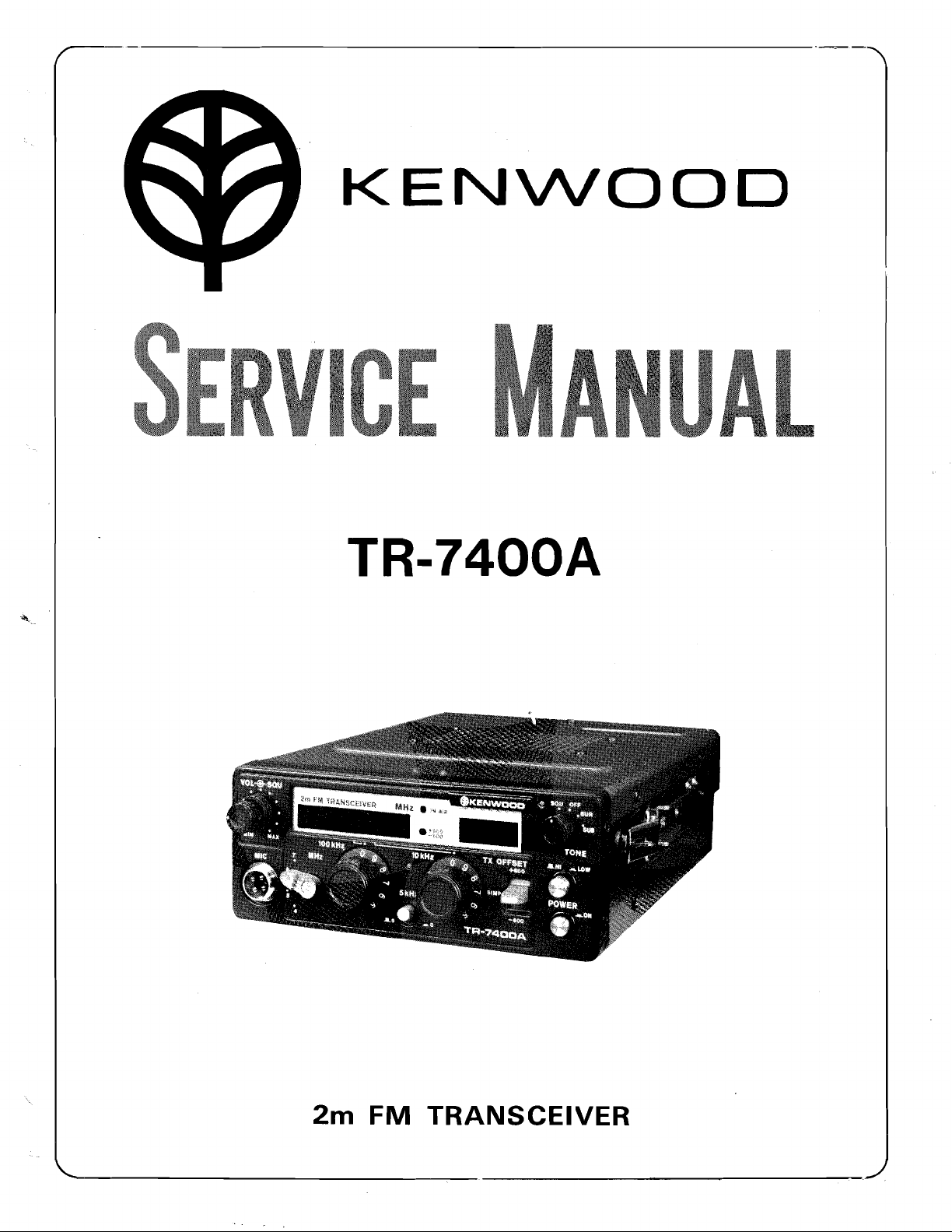
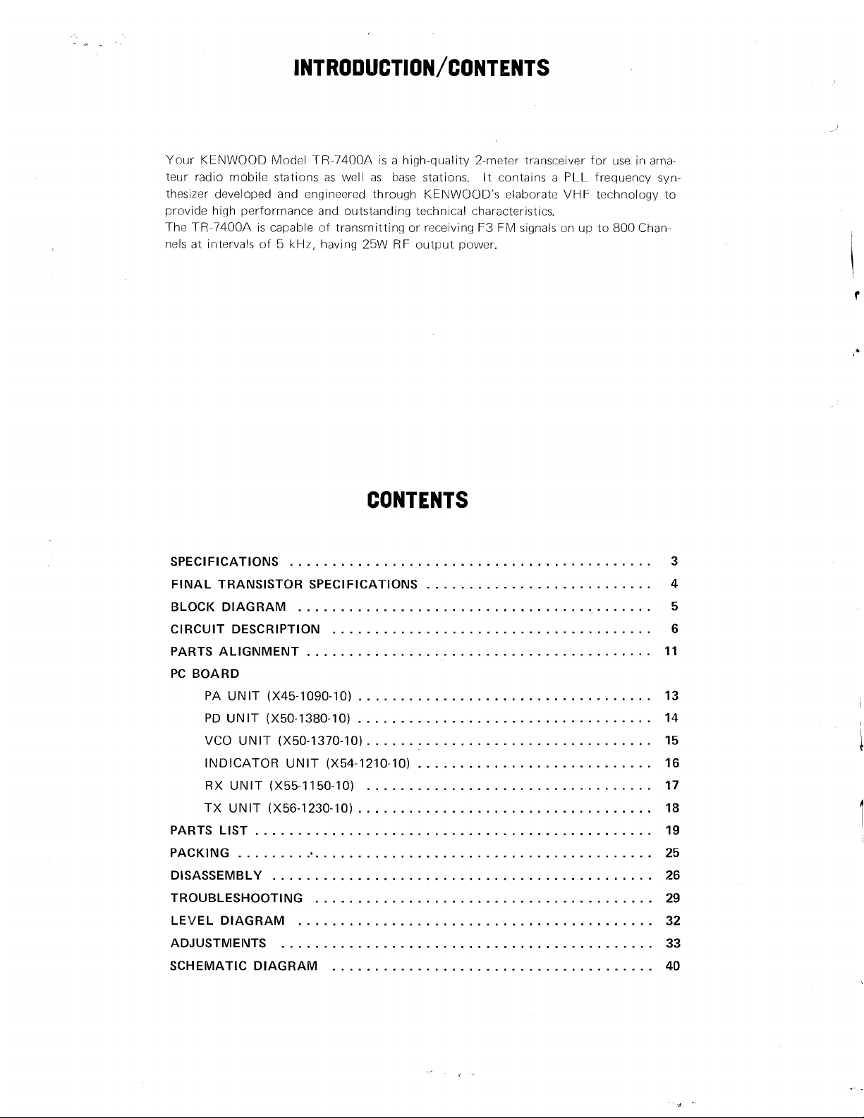
Your KENWOOD Model TR-7400A is a high-quality 2-meter transceiver for use in amateur radio mobile stations as well as base stations
thesizer developed and engineered through
provide high performance and outstanding technical characteristics
The TR-7400A is capable of transmitting or receiving F3 FM signals on up to
nels at intervals of 5 kHz. having 25W RF output power
KENWOOD's elaborate VHF technology to
.
It contains a
.
.
PLL
frequency syn-
800
Chan-
CONTENTS
SPECIFICATIONS
FINAL TRANSISTOR SPECIFICATIONS
BLOCK DIAGRAM
CIRCUIT DESCRIPTION
PARTS ALIGNMENT
PC BOARD
UNIT (X45-1090-10)
PA
PD UNIT (X50-1380-10)
VCO UNIT (X50.1370.10)
INDICATOR UNIT (X54-1210-10)
RX UNIT (X55-1150-10)
TX UNIT (X56-1230-10)
PARTS LIST
PACKING
DISASSENIBLY
TROUBLESHOOTING
LEVEL DIAGRAM
ADJUSTNIEIUTS
SCHEMATIC DIAGRAM
..................................................
...........................................
..........................................
......................................
.........................................
...................................
...................................
..................................
..................................
...................................
...............................................
........................................
........................................
........................................
............................................
......................................
...........................
............................
3
4
5
6
11
13
14
15
16
17
18
19
25
26
29
32
33
40
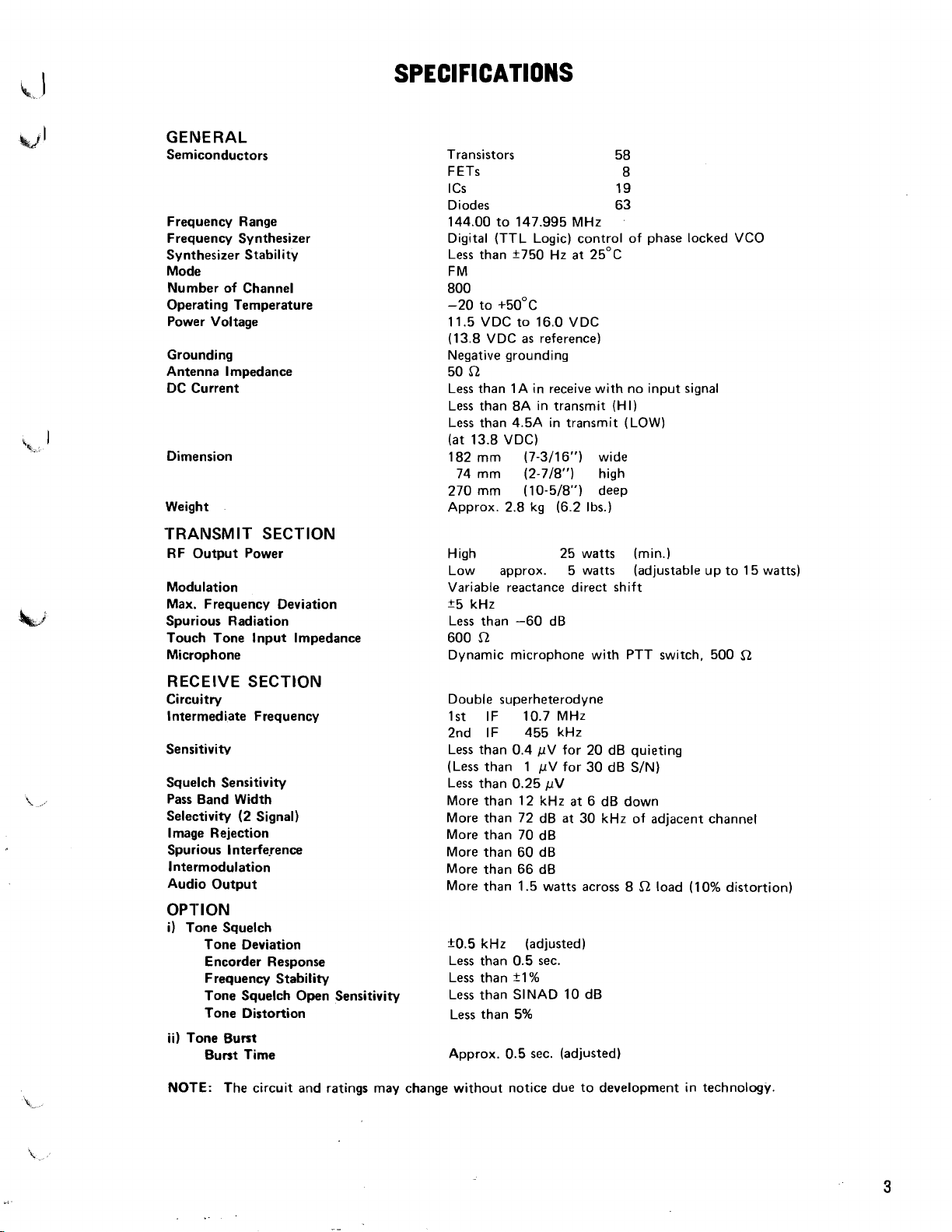
GENERAL
Semiconductors
Frequency Range
Frequency Synthesizer
Synthesizer Stability
Mode
Number of Channel
Operating Temperature
Power Voltage
Grounding
Antenna lmpedance
DC Current
Dimension
Weight
SPECIFICATIONS
Transistors 58
FETs 8
I Cs 19
Diodes 63
144.00 to 147.995 MHz
Digital (TTL Logic) control of phase locked VCO
Less than
FM
800
-20 to
11.5 VDC to 16.0 VDC
(13.8 VDC
Negative grounding
50
Less than 1A in receive with no input signal
Less than 8A in transmit (HI)
Less than
(at 13.8 VDC)
182 mm
74 mm
270
Approx. 2.8 kg (6.2
k750 Hz at 25"~
+50°c
as
reference)
52
4.5A in transmit (LOW)
(7-3116") wide
(2-718") high
mm
(10-518") deep
Ibs.)
TRANSMIT SECTION
RF Output Power High 25 watts (min.)
Low approx. 5 watts (adjustable up to 15 watts)
Modulation Variable reactance direct shift
k5
Max. Frequency Deviation
Spurious Radiation Less than -60 dB
Touch Tone Input Impedance 600
Microphone Dynamic microphone with PTT switch, 500
kHz
52
RECEIVE SECTION
Circuitry
Intermediate Frequency
Squelch Sensitivity
Pass Band Width
Selectivity
Image Rejection
Spurious Interference
lntermodulation
Audio Output
(2
Signal)
Double superheterodyne
1st IF 10.7 MHz
2nd IF 455
Less than 0.4 pV for 20 dB quieting
(Less than 1
Less than 0.25 ,uV
More than 12 kHz
More than 72 dB at 30 kHz of adjacent channel
More than 70 dB
More than 60 dB
More than 66 dB
More than 1.5 watts across 8
kHz
,uV for 30 dB SIN)
at
6 dB down
52
load (10% distortion)
OPTION
i) Tone Squelch
Tone Deviation
Encorder Response
Frequency Stability
Tone Squelch Open Sensitivity
Tone Distortion
ii) Tone Burst
Burst Time
k0.5 kHz (adjusted)
Less than 0.5
Less than 21%
Less than SlNAD 10 dB
Less than 5%
Approx. 0.5
sec.
sec. (adjusted)
52
NOTE: The circuit and ratings may change without notice due to development in technology.
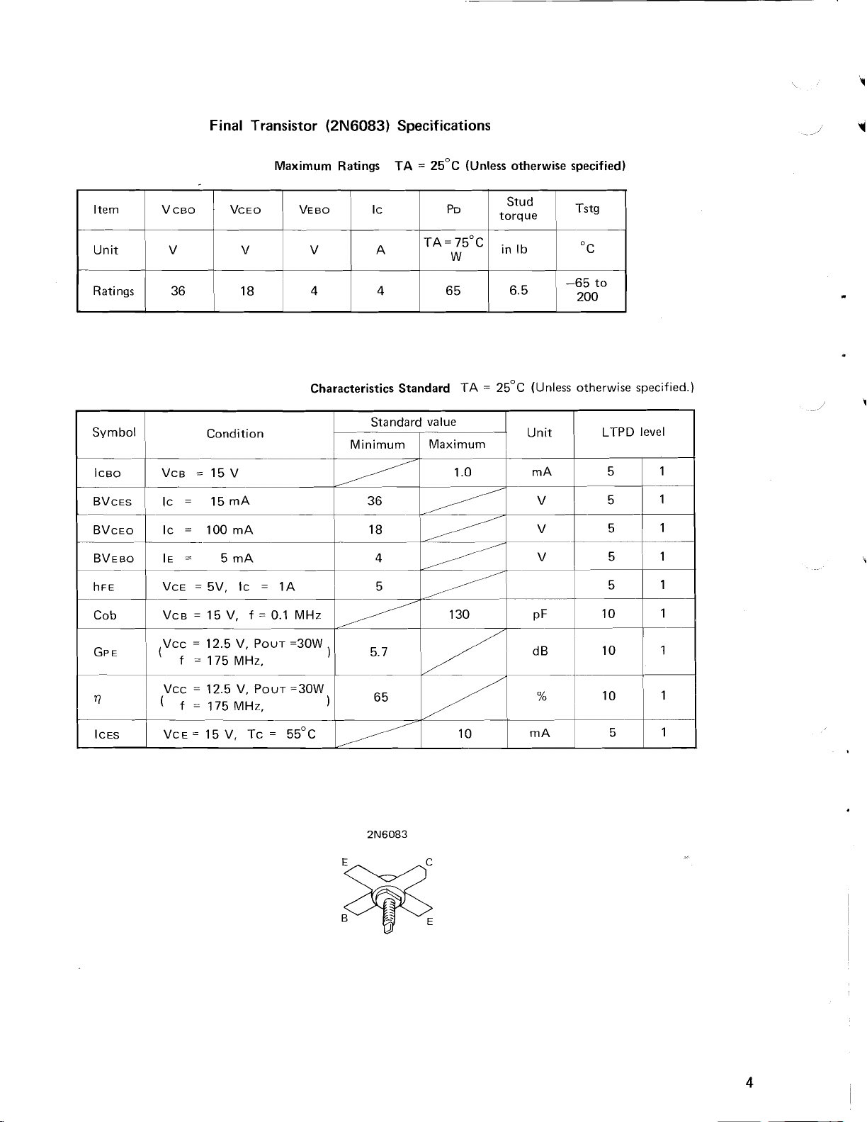
Item
V cso
Final Transistor
Maximum Ratings
VCEO
VEBO
(2N6083)
c
I
Specifications
TA
=
25O~ (Unless otherwise specified)
PD
Stud
torque
-
Tstg
Unit
Ratings
Symbol
ICBO
BVCES Ic
BVCEO
BVEBO
-
~FE
Cob
VCB = 15 V
1
Ic = 100 mA V
IE
VCE
VCB = 15V, f =0.1 MHz 1
Vcc
V
36
Condition
=
15 mA V
-
=
5 mA
=
5V,
=
12.5 V, POUT =30W
f
=
175 MHz,
V
18
V
4
Characteristics Standard TA
-
A
4
Standard value
Minimum
TA=~~"c
W
6 5
Maximum
4
IC
=
1A 5 5 1
)
5.7 dB 10 1
/
inIb
6.5
=
25OC (Unless otherwise specified.)
Unit
rn
,
V
"c
-65 to
200
A
LTPD level
5
5
5
1
1
rl
ICES
Vcc
=
12.5 V, POUT =30W
=
175 MHz,
f
VCE= 15 V, TC = 55OC 10 mA 5 1
1
6 5
%
10 1
RX UNlT (X55-1150-10)
r-
-----------
I
I
I
I
L
,,-,---,-----------,
RXA LR
PLL
-
r-----------b
I
VCO
UNlT (X50-1370-10)
SELECTOR
-
---------------
'
I
I
TX UNIT (~56-1230-10)
ZSC458 2SC458
+--<&--,
TS SMI
BURST
BLOCK
--------
s1
S2 S3 TI0
sau
VRA
DIAGRA!
TXB
a
V
I
T-----~----
I
I
I114171919151
I
L--------,-
DISPLAY UNIT (X54-1210- 10)
DISPLAY UNIT (X54-
TLR-313x6
r----------
I
I
I
-t
600
DEC. DRIVER
SN7447AN X 3
- - - - -
I
I
I
SWITCH BOARD
I I
-1
I
I
J
121
0-
10)
1
-
- - - - - -
~lvl~-N(1/537- 1/936)
TX OFFSET LOGIC
I
(BCD 400-799)
- - -
pw
A
I
- - - - - -
MC74416X3
13.8V
-
-
POWER SW
-
zsc460
BUFF
- - - -
VCO
UNlT (X50-
r------
2SC460 ZSC460
!
I
-
-.(b
AMP
T'
-
UNIT
(~50-1380-10)
'
1
I
,
T
22%
l
OkHz
2.56MHz 160 kHz
REFOSC,l/2 1/16 1/16
I
TD3400
- - - -
H
TD3493 TD3493
- - - - -
-
-
- - - - - -
P.D
A
MC4044P
I
1~15%
2~~733
- - - - -- - -
UNIT
_
--------
(~50-1370-10)
_-_---
----------
---
----
-------
1
I
I
I
I
I
I
TX, RX
MIXER
D
k,*,j
2
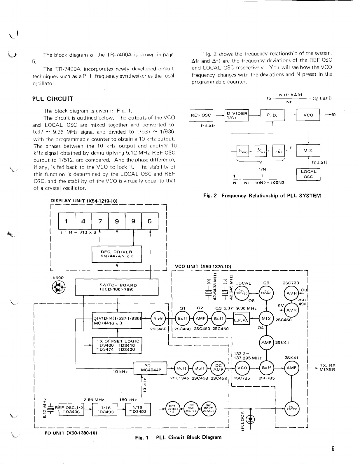
shows the frequency relationship of the system.
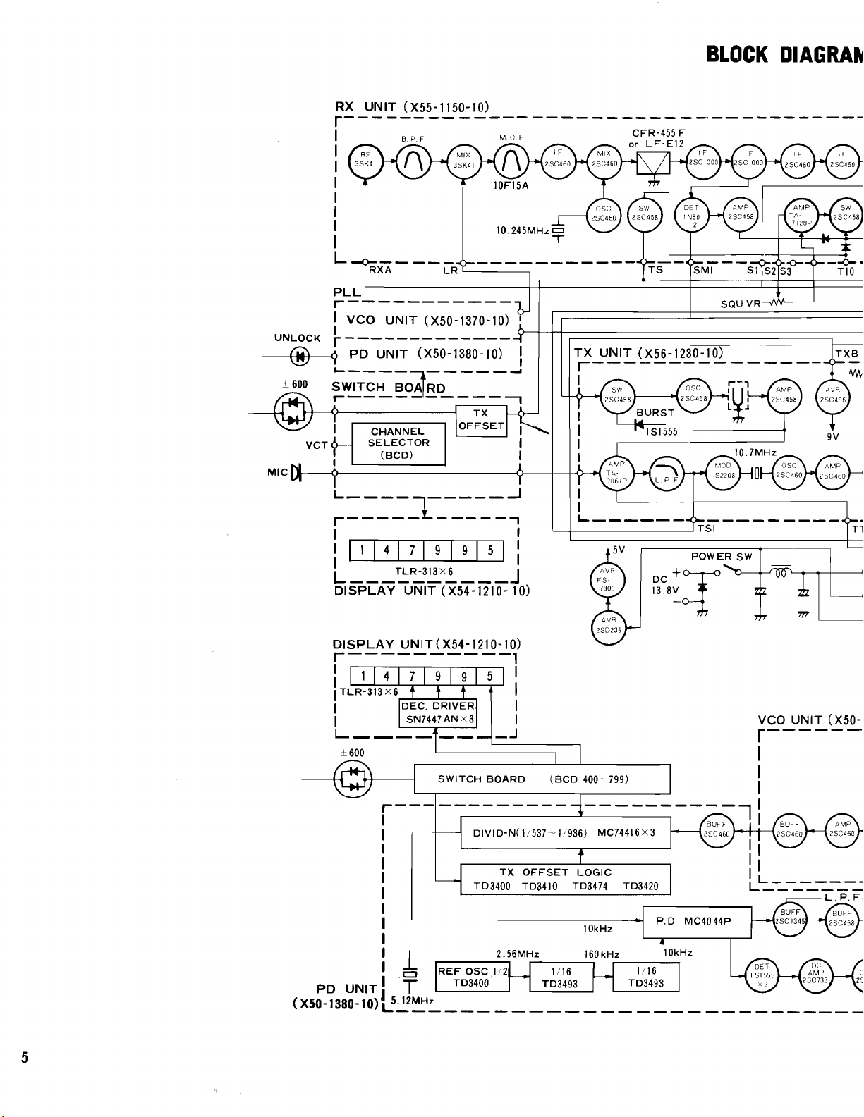
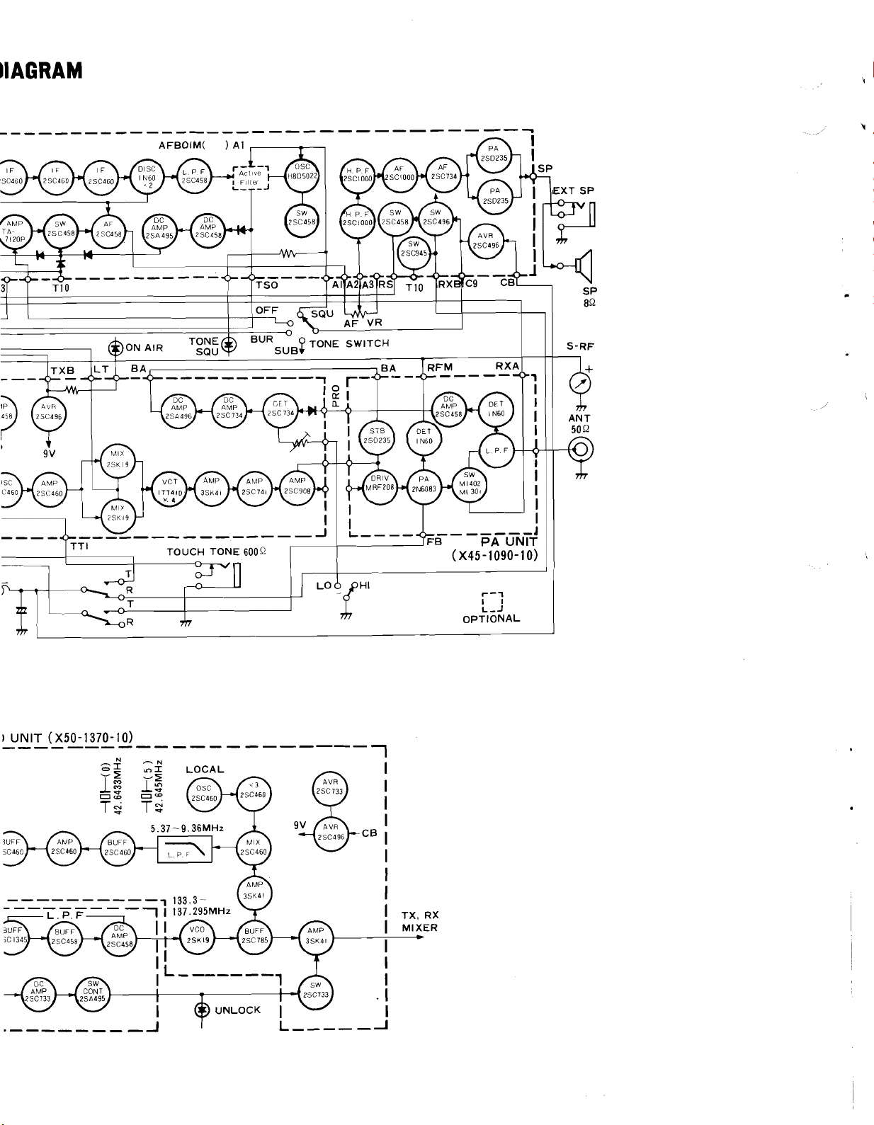
The block diagram of the TR-7400A is shown in page
5.
The TR-7400A incorporates new1 y developed circuit
techniques such as a PLL frequency synthesizer as the local
oscillator. programmable counter.
PLL
CIRCUIT
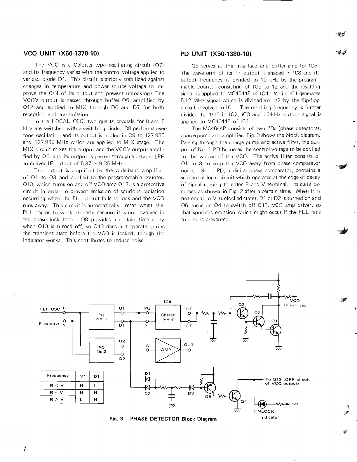
The block diagram is given in Fig. 1.
The circuit is outlined below. The outputs of the VCO
and LOCAL OSC are mixed together and converted to
--
5.37
with the programmable counter to obtain a 10 kHz output.
The phases between the
kHz signal obtained by demultiplying 5.12 MHz REF OSC
output to
if any, is fed back to the VCO to lock it. The stability of
this function is determined by the LOCAL OSC and REF
OSC, and the stability of the
of a crystal oscillator.
9.36 MHz signal and divided to 1/537
10 kHz output and another 10
11512, are compared. And the phase difference,
VCO is virtually equal to that
DISPLAY
r------------
UNlT
(X54-1210-10)
--
If936
Fig.
Afr and
and LOCAL
frequency changes with the deviations and
REF
El
Af,! are the frequency deviations of the REF OSC
OSC respectively. You will see how the VCO
-
OSC
Fig. 2 Frequency Relationship of PLL
DIVIDER
1/Nr
1
fo
P.
=-----
D.
I
N
N (fr +Afr)
Nr
preset in the
+
(41
+Of
LOCAL
SYSTEM
9.)
I
I
PD
UNlT
2.56
(X50-1380-10)
MHz
Fig.
UNlT
PLL Circuit Block Diagram
1
(X50-1370-10)
----
-
TX. RX
*MIXER
VCO
UNlT
(X50-1370-10)
PD
UNlT
(X50-1380-10)
The VCO is a Colpitts type oscillating circuit (07)
and its frequency varies with the control voltage applied to
varicap diode
Dl. This circuit is strictly stabilized against
changes in temperature and power source voltage to improve the
C/IU of its output and prevent unlocking.. The
VCO's output is passed through buffer 06, amplified by
012 and applied to MIX through D6 and D7 for both
reception and transmission.
In the LOCAL OSC, two quartz crystals for
0 and 5
kHz are switched with a switching diode. 08 performs overtone oscillation and its output is tripled in 09 to 127.930
and 127.935 MHz which are applied to MIX stage. The
lMlX circuit mixes the output and the VCO's output amplified by 05, and its output is passed through a
to deliver
IF output of 5.37 - 9.36 MHz.
.rr-type LPF
The output is amplified by the wide-band amplifier
of
01 to 03 and applied to the programmable counter.
013, which turns on and off VCO amp 012, is a protective
circuit in order to prevent emission of spurious radiation
occurring when the PLL circuit fails to lock and the VCO
runs away. This circuit
PLL begins to work properly because
is
automatically reset when the
it
is not involved in
the phase lock loop. D8 provides a certain time delay
when 013 is turned off, so 013 does not operate during
the transient state before the VCO is locked, though the
indicator works. This contributes to reduce noise.
06 serves as the interface and buffer amp for IC8.
The waveform of its IF output is shaped in IC8 and its
output frequency is divided to 10 kHz by the program-
mable counter consisting of IC5 to 12 and the resulting
signal is applied to
5.12 MHz signal which is divided
circuit involved in
divided to 1/16 in
applied to
MC4044P of IC4.
MC4044P of IC4. While IC1 generates
.to 112 by the flip-flop
IC1. The resulting frequency is further
IC2, IC3 and 10-kHz output signal is'
The MC4044P consists of two PDs (phase detectors),
charge pump and amplifier. Fig. 3 shows the block diagram.
Passing through the charge pump and active filter, the output of No. 1 PD becomes the control voltage to be applied
to the varicap of the VCO. The active filter consists of
01 to 3 to keep the VCO away from phase comparator
noise. No. 1 PD, a digital phase comparator, contains a
sequential logic circuit which operates at the edge of decay
of signal coming to enter
comes as shown in Fig. 2 after a certain time. When
not equal to V (unlocked state),
R
and V terminal. Its state be-
Dl or D2 is turned on and
R
05 turns on 04 to switch off 013, VCO amp driver, so
that spurious emission which might occur if the
PLL fails
to lock is prevented.
-
vd
is
REF
P--
OSC
C4 VCO
U
1
Fig.
m
V
A
Dl
w
3
1
-
"
-
fi
-
PD
No.
No.2
PU U F
-
r\
-"
-
Charge
pump
w
PD D F
PHASE DETECTOR
w
w
Block
Diagram
04
;
-
UNLOCK
To
013 (OFF
VCO
of
Indicator
0
To vari cap.
output)
5
v
circuit
I
w
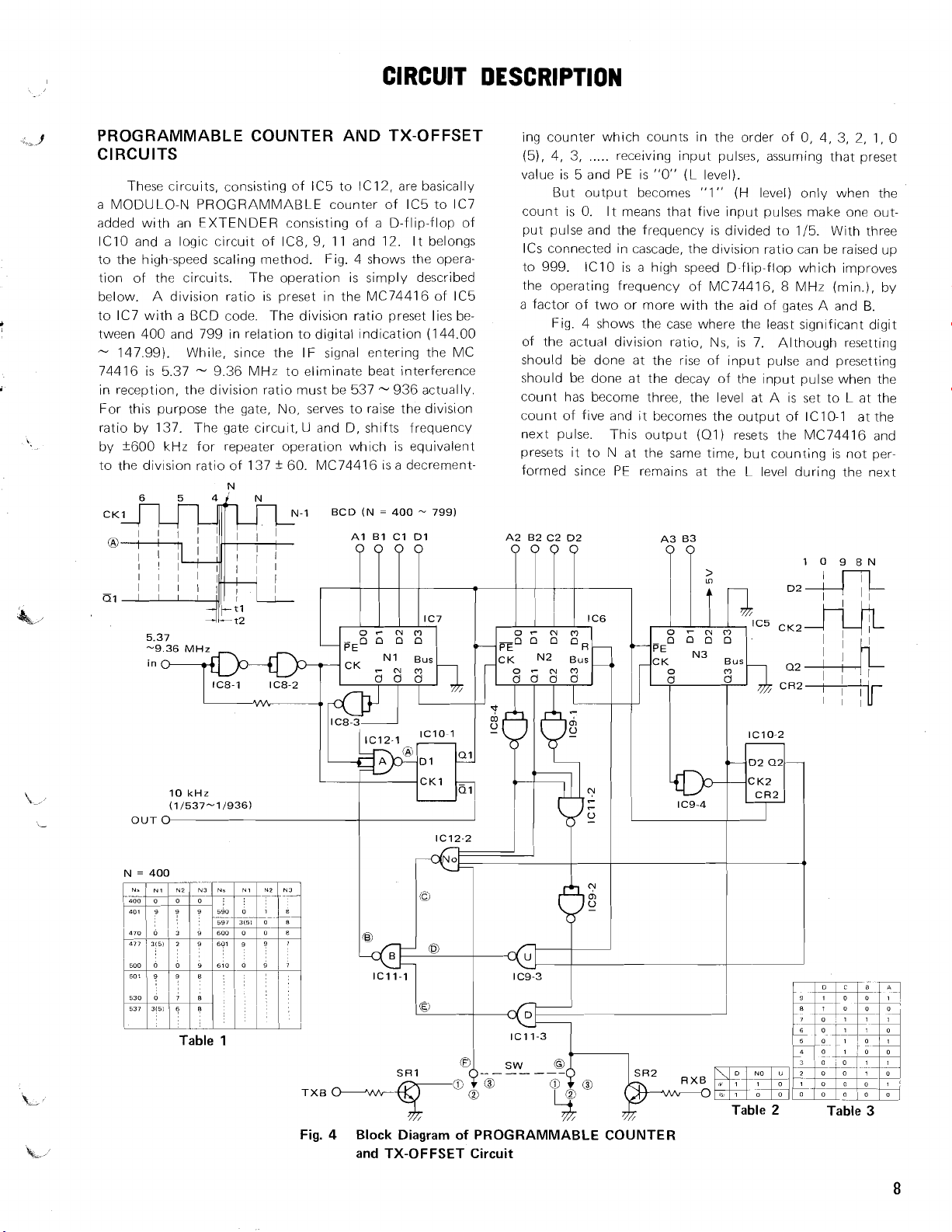
PROGRAMMABLE COUNTER AND TX-OFFSET
CIRCUITS
These circuits, consisting of IC5 to
a MODULO-N PROGRAMMABLE counter of IC5 to
added with an EXTENDER consisting of a D-flip-flop of
lClO and a logic circuit of IC8, 9,
to the high-speed scaling method. Fig. 4 shows the operation of the circuits. The operation is simply described
below.
to IC7 with a BCD code. The division ratio preset lies between 400 and 799 in relation to digital indication (144.00
-
74416 is 5.37
in reception, the division ratio must be 537
For this purpose the gate, No, serves to raise the division
ratio by 137.
by
to the
A division ratio is preset in the
147.99). While, since the IF signal entering the MC
-
9.36 MHz to eliminate beat interference
The gate circuit,
f600
kHz
for repeater operation which is equivalent
div~sion ratio of 137 f 60. MC74416 is a decrement-
U
IC12, are basically
I I
and 12.
MC74416 of IC5
-
and D, shifts
IC7
It belongs
936 actually.
frequency
ing counter which counts in the order of 0, 4, 3, 2,
(5), 4, 3,
value is 5 and
count is
put pulse and the frequency is divided to
ICs connected in cascade, the division ratio can be raised up
to 999.
the operating frequency of
a factor of two or more with the aid of gates A and
of the actual division ratio, Ns, is 7.
should be done at the rise of input pulse and presetting
should be done at the decay of the input pulse when the
count has become three, the level at A
count of five and it becomes the output of
next pulse. This output
presets it to N at the same time, but counting is not performed since PE remains at the L level
.....
receiving input pulses, assuming that preset
PE
is "0" (L level).
But output becomes
0. It means that five input pulses make one out-
IClO is a high speed D-flip-flop which improves
Fig. 4 shows the case where the least significant digit
"1" (H level) only when the
115. With three
MC74416, 8 MHz (min.), by
Although resetting
is
set to L at the
IC10-1 at the
(01) resets the MC74416 and
during the next
1,
B.
0
Fig. 4 Block Diagram of PROGRAMMABLE COUNTER
and TX-OFFSET Circuit
CIRCUIT DESCRIPTIONS
input pulse and it is reset. The operating frequency has
been improved because resetting and presetting are done
in one cycle of input pulse
delay time, t2, of the high speed D-flip-flop in
much smaller than the delay time, tl, from
7 and logic circuit to point A.
Next, operation is explained in relation to the TX off-
set switch setting.
1
+600
During reception, this is the same as in (2).
transmission,
Gate U therefore opens and gates No and D are closed.
At this setting, Ns
as an extender when
5 respectively, to perform division of N
2
No
(F) and (G) make up No in Table 2. Gates No and U
open and gate D
Ns
=
N + 137, holds between preset value N and actual division ratio Ns. It is enough to decrement the counter after
division of N
resetting and presetting just when the count has become
137. For this purpose,
8,
6 and 3 respectively (as already described), but it
operates as an extender at code 5 and performs division
of N
+
extender operates
3
-600
During reception, SR2 is turned on as in (2). During
transmission, gates
At this setting, Ns
extender to perform division of N
IC7 carry code 9,
extender operates at code 77 even when all gates are open
Table 1 shows the case of
-
SR 1 is turned on and becomes U in Table 2.
=
(SIMP)
IS
(decrernenting) has completed and perform
137. Since the gate is of code 197 (137 + 60), the
before this code triggers the circuitry.
No, U and D open as D in Table
=
2
TSBl
but not in half a cycle, and the
lClO is
IC5, 6 and
During
IN + 197 (137 + 60), and it operates
IC5, IC6 and IC7 take code
+
197.
closed. At this setting, the relation,
IC5, IC6 and IC7 do not take code
N
+
77 (137 - 60), it operates as an
+
77 when IC5, IC6 and
and 5 respectively. At this time, the
N
=
400 (144.00 MHz).
Active
n
filter
8,
0 and
2.
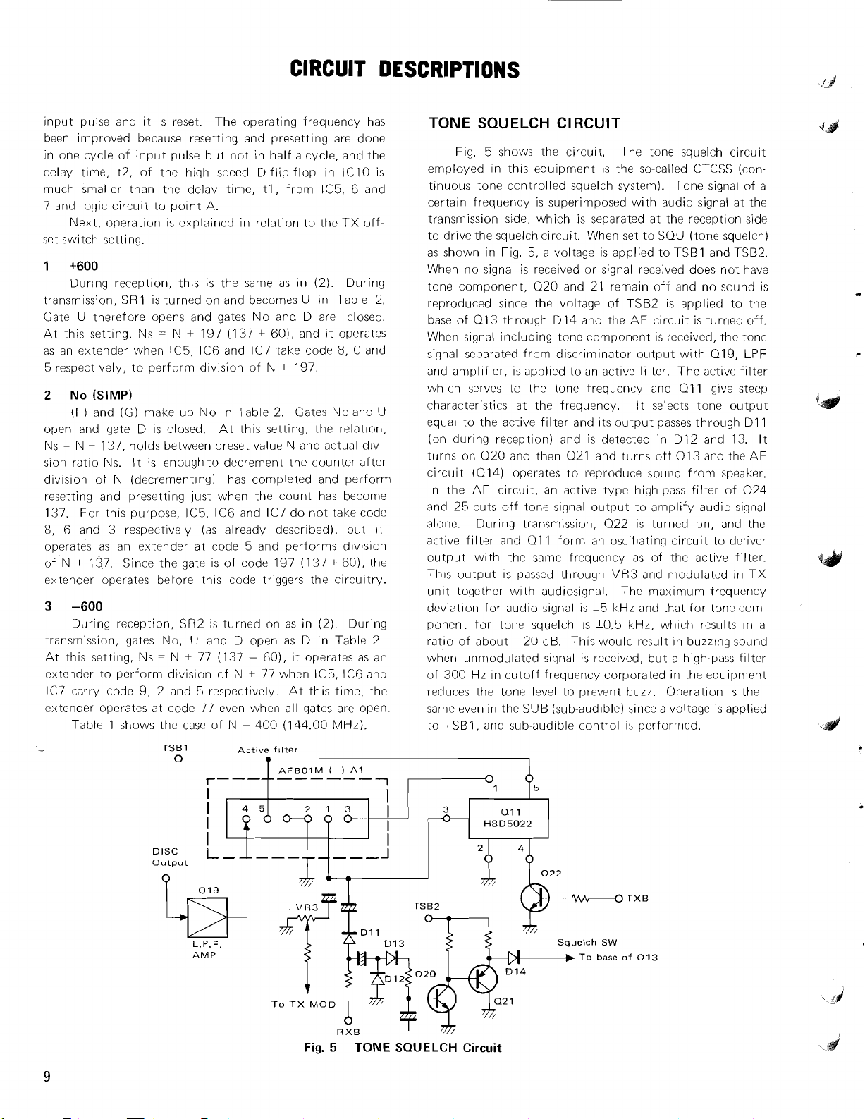
TONE SQUELCH CIRCUIT
Fig. 5 shows the circuit. The tone squelch circuit
019,
output
(con-
LPF
024
TX
employed in this equipment is the so-called CTCSS
tinc~oc~s tone controlled squelch system). Tone signal of a
certain frequency
trans~rlission side, which is separated at the reception side
to drive the squelch circuit. When set to
as shown in Fig. 5, a voltage is applied to
When no signal is received or signal received does not have
tone component, 020 and 21 remain off and no sound is
reproduced since the voltage of TSB2 is applied to the
base of Q13 through
When signal including tone component is received, the tone
signal separated from discriminator output with
and amplifier, is applied to an active filter. The active filter
which serves to the tone frequency and
characteristics at the frequency. It selects tone
equal to the active filter and its output passes through Dl 1
during reception) and is detected in Dl2 and 13. It
(on
turns on
circuit
In
and 25 cuts off tone signal output to arnplify audio signal
alone. During transmission,
active filter and
output with the same frequency as of the active filter.
This
unit together with audiosignal. The maximum frequency
deviation for audio signal is
ponent for tone squelch is
ratio of about -20 dB. This would result in buzzing sound
when unmodulated signal is received, but a high-pass filter
of 300 Hz in cutoff frequency corporated in the equipment
reduces the tone level to prevent buzz. Operation is the
same even in the SUB (sub-audible) since a voltage is applied
to
020 and then 021 and turns off Q13 and the AF
(014) operates to reproduce sound from speaker.
the AF circuit, an active type high-pass filter of
oc~tpc~t is passed through VR3 and modulated in
TSBI, and sub-audible control is performed.
is
superimposed with audio signal at the
SOU (tone squelch)
TSBI and TSB2.
Dl4 and the AF circuit is turned off.
01 1 give steep
022 is turned on, and the
01 1 forin an oscillating circuit to deliver
f5 kHz and that for tone com-
k0.5 kHz, which results in a
*d
Dlsc
Output
e
L.P.F.
AMP
I
I
L
I
2
13
---A
Fig. 5 TONE SQUELCH Circuit
I
H8D5022
To
base
of
013
DESCRIPTION
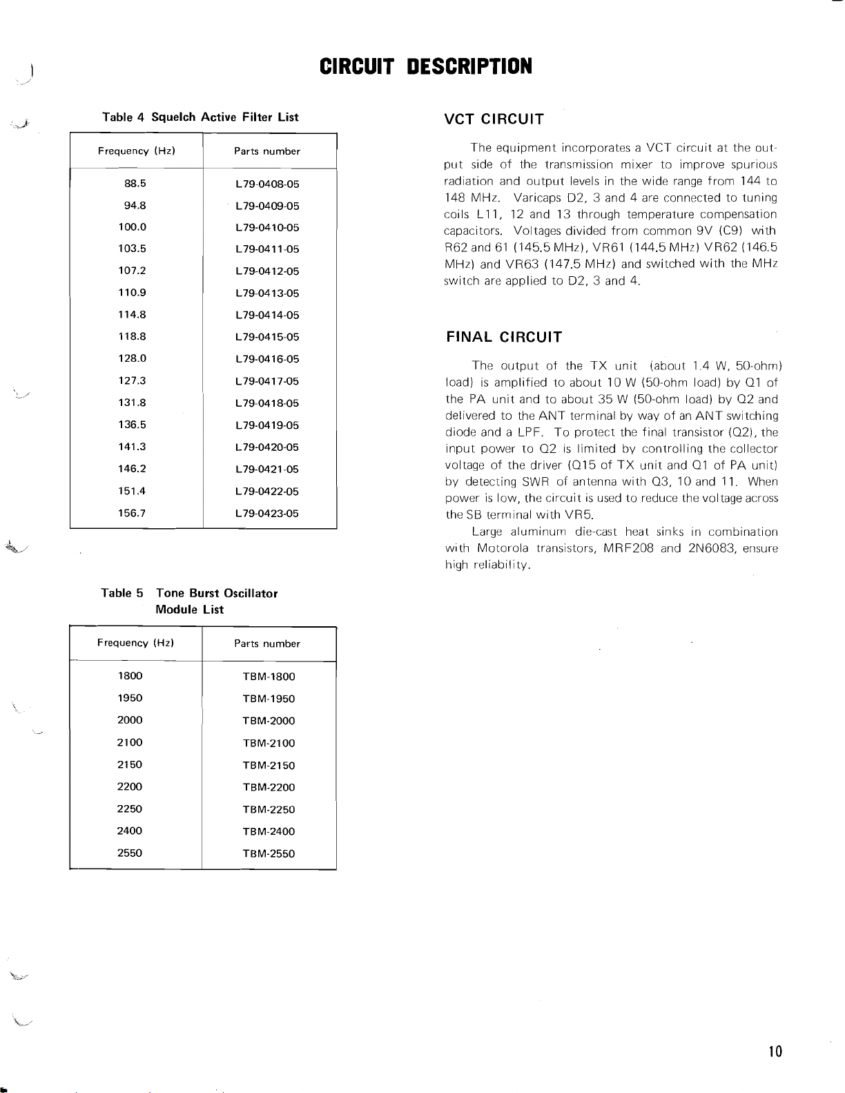
Table 4 Squelch Active Filter List
Frequency
88.5
94.8
100.0
103.5
107.2
110.9
114.8
118.8
128.0
127.3
131.8
136.5
141.3
146.2
151.4
156.7
(Hz)
Parts number
L79-0408-05
L79-0409-05
L79-0410-05
L79-0411-05
L79-0412-05
L79-0413-05
L79-0414-05
L79-0415-05
L79-0416-05
L79-0417-05
L79-0418-05
L79-0419-05
L79-0420-05
L79-0421-05
L79-0422-05
L79-0423-05
VCT CIRCUIT
The equipment incorporates a VCT circuit at the output side of the transmission mixer to improve spurious
radiation and output levels in the wide range from 144 to
148 MHz. Varicaps D2, 3 and 4 are connected to tuning
coils
L11, 12 and 13 through temperature compensation
capacitors. Voltages divided from common
9V (C9) with
R62 and 61 (145.5 MHz), VR61 (144.5 MHz) VR62 (146.5
MHz) and VR63 (147.5 MHz) and switched with the MHz
switch are applied to D2, 3 and 4.
FINAL CIRCUIT
The output of the TX unit iabout 1.4 W, 50-ohm)
load) is amplified to about 10 W (50-ohm load) by 01 of
the PA unit and to about 35 W (50-ohm load) by 02 and
delivered to the ANT terminal by way of an ANT switching
diode and a LPF. To protect the final transistor
input power to 02 is limited by controlling the collector
voltage of the driver (015 of TX unit and
by detecting SWR of antenna with 03, 10 and 11.
power is low, the circuit is used to reduce the voltage across
the
SB terminal with VR5.
Large aluminum die-cast heat sinks
w~th Motorola transistors, MRF208 and 2N6083, ensure
high reliability.
(02), the
01
of PA unit)
When
In combination
Table
5
Frequency
1800
1950
2000
2100
21 50
2200
2250
2400
2550
Tone Burst Oscillator
Module List
(Hz)
Parts number
TBM-1800
TBM-1950
TBM-2000
TBM-2100
TBM-2150
TBM-2200
TBM-2250
TBM-2400
TBM-2550
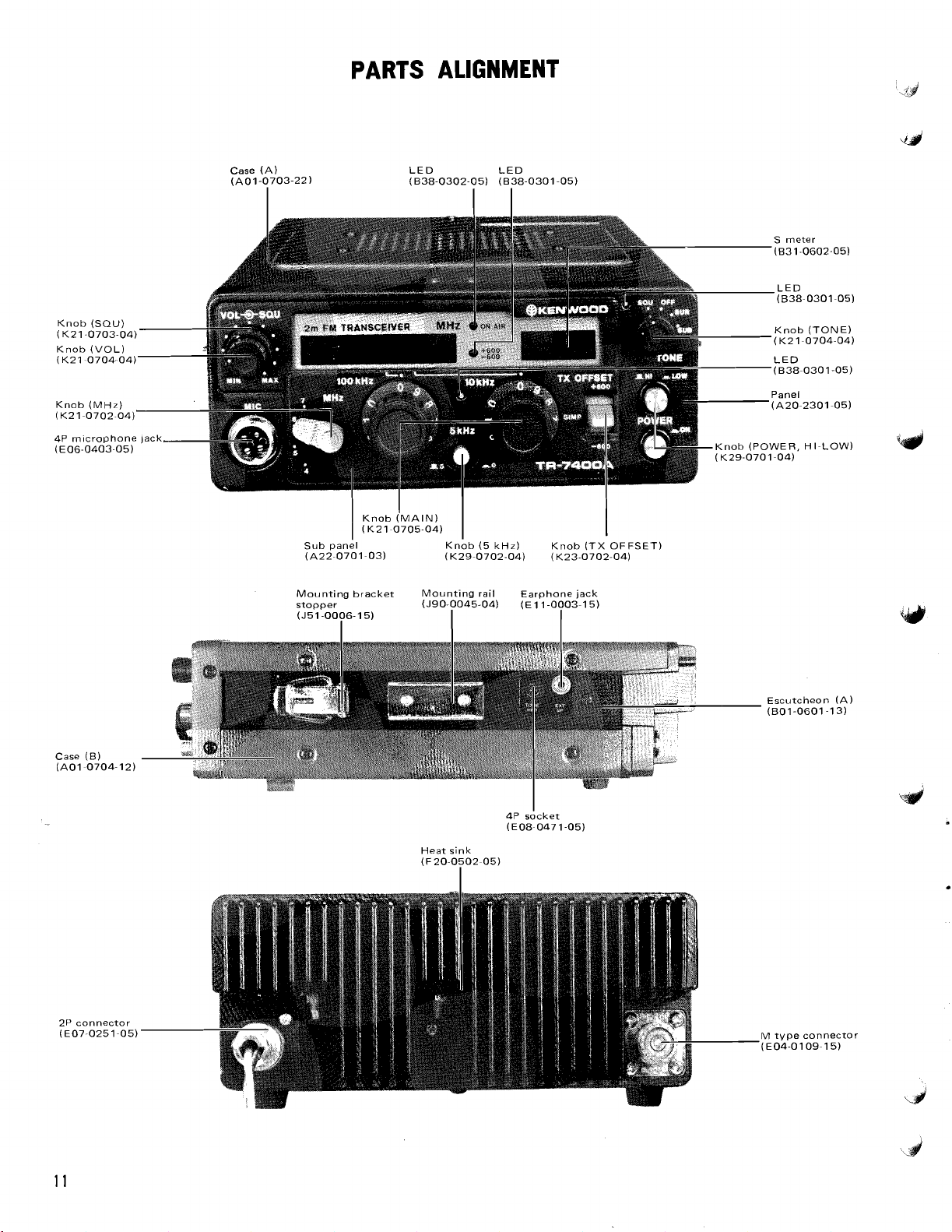
PARTS ALIGNMENT
Knob (SQU)
(K21-0703-04)
Knob (VOL)
(K2 1-0704-04)
Knob (MHz)
(K2 1-0702-04)'
4P microphone
(E06-0403-05)
Case (A)
(A01-0703-22)
LED LED
(838-0302-05) (838-0301-05)
Knob (MAIN)
(K21~0705-04)
'1
sub panel Knob (5 kHz)
(A22-0701~03) (K29-0702-04)
Mounting bracket Mounting rail Earphone jack
stopper
(J51-0006-15)
I
(J90-0045-04) (E 11-0003-1 5)
I
Knob (TX OFFSET)
(K23-0702-04)
I
Case (8)
(A01-0704.12)
2P connector
(E07-0251-05)
Heat sink
(F
20-0502-05)
I
4P socket
(E08~047 1-05)
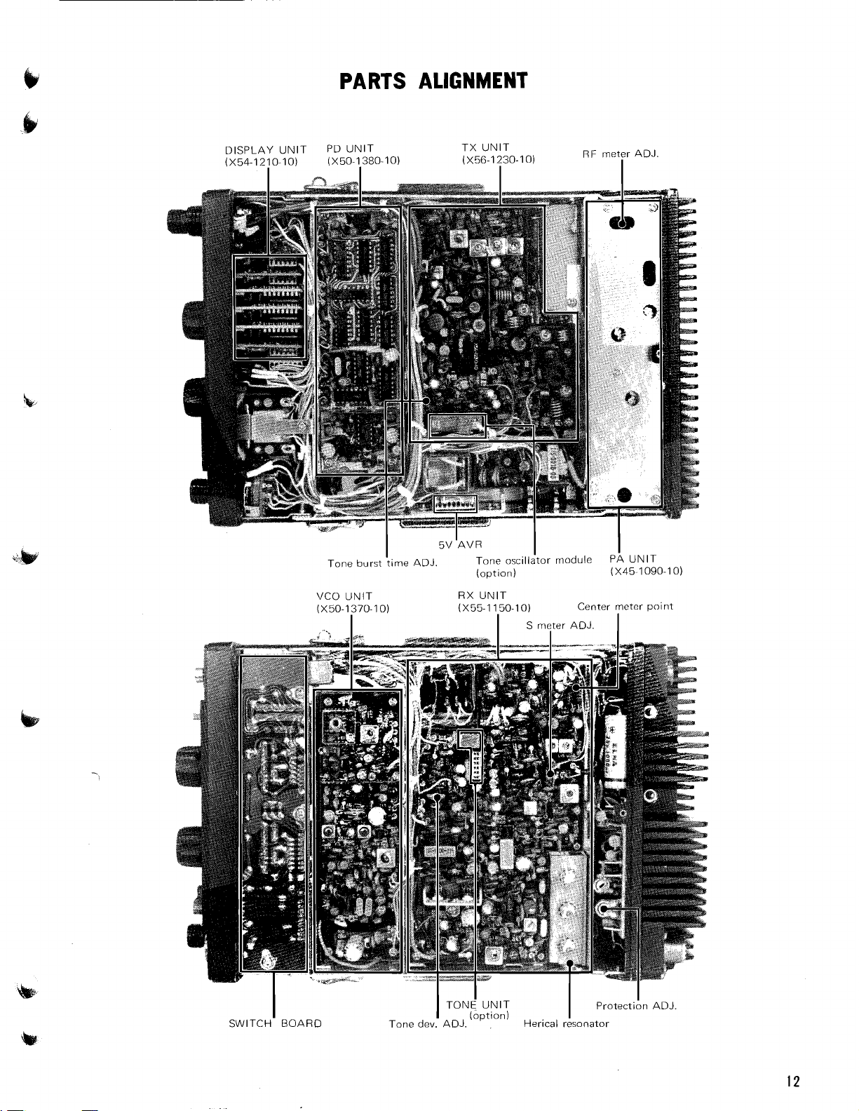
PARTS ALIGNMENT
DISPLAY UNlT PD UNlT
(X54-1210-10) (X50-1380-10)
VCO UNIT RX UNIT
(X50-1370-10) (X55-1 150-10)
I
Tone burst time ADJ.
I
I
TX UNlT
(X56-1230-10)
I
~V'AVR
Tone oscillator module PA UNlT
(option)
I
I
s
meter ADJ.
RF meter ADJ.
I
I
(X45-1090-10)
Center meter point
I
TON<
SWITCH BOARD Tone dev. ADJ. Herical resonator
I
I
UNIT
loption)
I
~rotecti6n ADJ
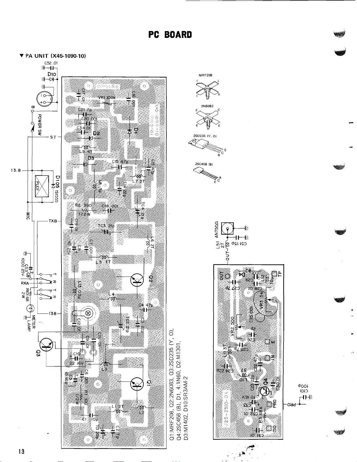
V
PA
UNIT
GC
(X45-1090-10)
PC
BOARD
 Loading...