Kenwood RXDV-252 Service manual
MINI HiFi COMPONENT SYSTEM
70%
RXD-V252/V252-H
SERVICE MANUAL
(XD-V252)**
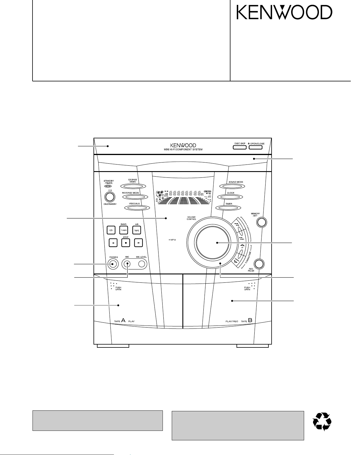
FRT cab ass'y *
(A60-)
FL panel *
(B10-)
© 2001-10 PRINTED IN KOREA
B51-5759-00 (K/K) 404
Panel(VCD)
(A60-2220-08)
Phone jack
(E11-0942-08)
Jack(MIC)
(E11-0953-08)
Cassette lid(L)
(A21-3958-08)
**Refer to page 2 if you want to know system configuration.
In compliance with Federal Regulations, following are reproduction of labels on, or inside the product relating to laser
product safety.
Knob(VOLUME)
(K29-8047-08)
Dress ring
(A21-3966-08)
Cassette lid(R)
(A21-3959-08)
* Refer to parts list on page 27.
KENWOOD-Corp. certifies this equipment conforms to DHHS
Regulations No.21 CFR 1040. 10, Chapter 1, subchapter J.
DANGER : Laser radiation when open and interlock defeated.
AVOID DIRECT EXPOSURE TO BEAM.
RXD-V252/V252-H
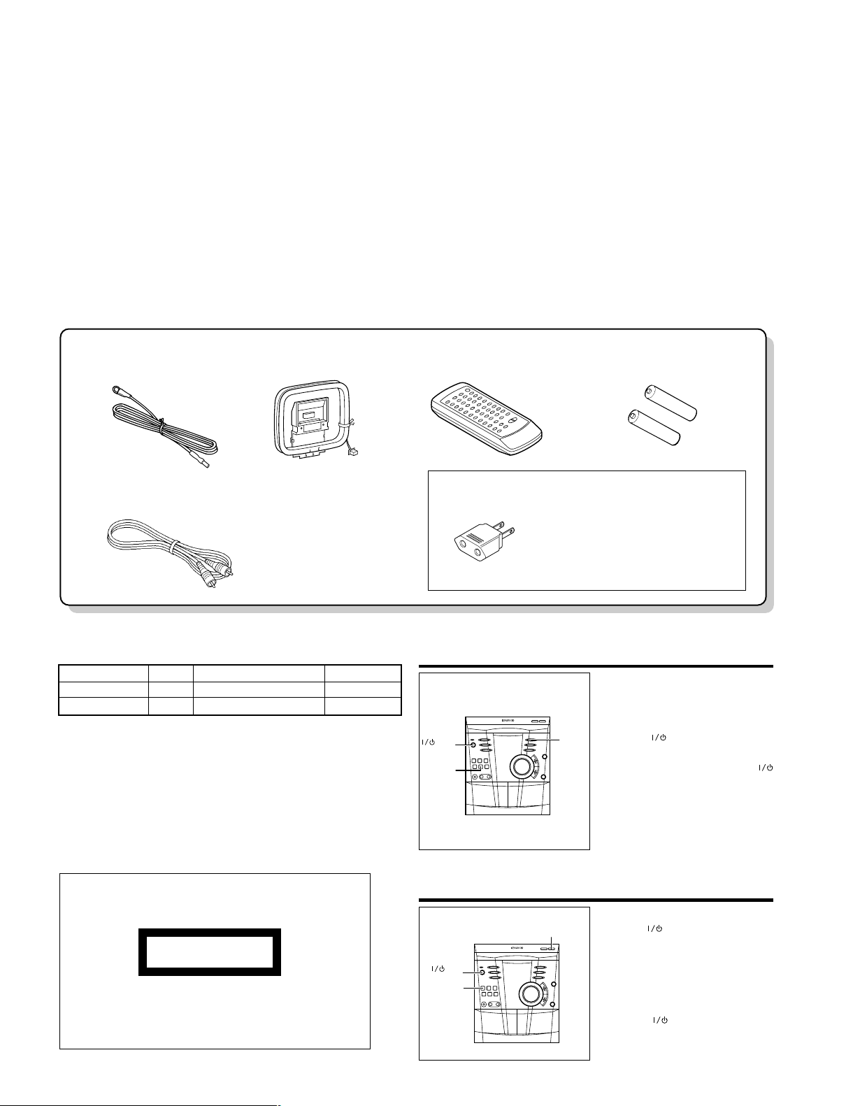
AC Plug Adaptor (1)
(E03-0115-05)
Use to adapt the plug on the
power cord to the shape of the
wall outlet.
(Accessory only for regions where
use is necessary.)
AM Loop Antenna(1)
(T90-0879-08)
"AA" size battery(2)
(UM/SUM-3, R6, HP-7 or similar)
Remote Control(1)
(A70-1574-08)
FM Antenna(1)
(T90-0883-08)
Video Cable(1)
(E30-7255-08)
The marking of products using lasers
(Except for some areas)
The marking is located on the rear panel and
says this product has been classified as Class
1. It means that there is no danger of hazardous radiation outside the product
CLASS 1
LASER PRODUCT
RESETTING THE MICROCOMPUTER
Reset the microcomputer under the following conditions :
• To erase all of the stored memory contents (clock
and timer settings, and tuner and CD presets).
• If the display is not correct.
• If the operation is not correct.
1 Press the ON/STANDBY button to enter
the standby mode.
2 Whilst pressing down the 7 STOP button and
the SOUND MODE button, hold down the
ON/STANDBY button for at least 1 second.
• “CLEAR AL” will appear .
Caution :
•
The operation explained above will erase all data
stored in memory including clock and timer settings, and tuner and CD presets.
TRANSPORTING THE UNIT
Before you move this product to a new location,
proceed as follows :
1 Press the ON/STANDBY button to turn the
power on.
2 Press the CD button.
3 Press the 0 OPEN/CLOSE button to open the
disc tray.
• Remove all CDs inserted in the unit.
4 Press the 0 OPEN/CLOSE button to close the
disc tray.
• Make sure that “NO DISC” is displayed.
5 Press the ON/STANDBY button to enter
the standby mode and then unplug the AC power
cord from the AC socket.
SOUND
MODE
ON/
STANDBY
7 STOP
ON/
STANDBY
CD
0 OPEN/CLOSE
CONTENTS / ACCESSORIES / CAUTIONS
Contents
CONTENTS / ACCESSORIES / CAUTIONS............. 2
EXTERNAL VIEW .......................................................3
CIRCUIT DESCRIPTION ............................................4
ADJUSTMENT ............................................................7
WIRING DIAGRAM .....................................................8
Attention
Please contact our KENWOOD Service Department in your side if you want the service information; Circuit Description. Full
Described Parts list and so. Information is available to you by internet from us.
Accessories
PC BOARD ................................................................ 9
SCHEMATIC DIAGRAM .......................................... 15
EXPLODED VIEW ....................................................25
PARTS LIST..............................................................27
SPECIFICATIONS ......................................Back cover
System Configurations
Model Color M(General Market) I(Malaysia)
RXD-V252 Blue - I
RXD-V252-H Gray M I2
Cautions
2
ANTENNA
AM
LOOP
FM
75
VIDEO
/AUX
VIDEO
OUT
SPAN
SELECTOR
230V
240V
FM 50kHz
AM 9kHz
FM 100kHz
AM 10kHz
+
+
-
-
-
L
SPEAKERS
RATED SPEAKER IMPEDANCE:
6 OHMS MIN.
R
LR
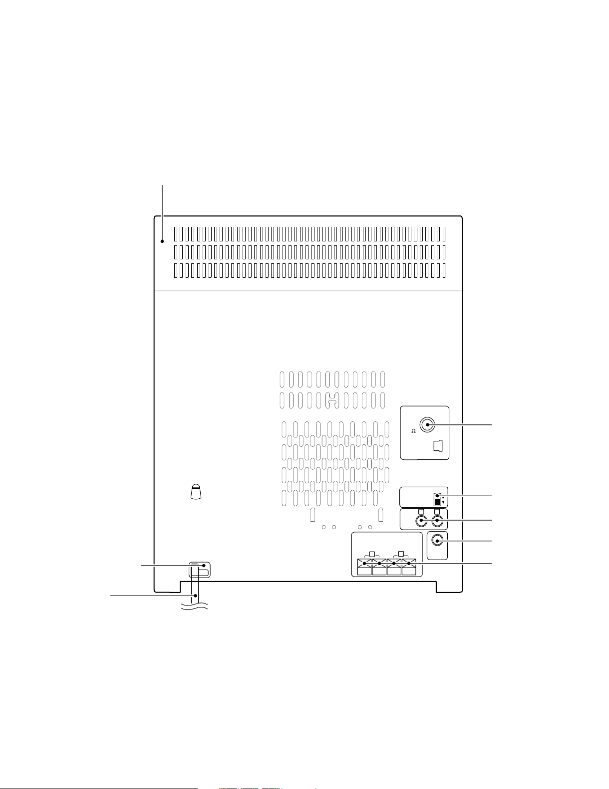
Cabinet(TOP)
(A02-3014-08)
RXD-V252/V252-H
EXTERNAL VIEW
AC power cord bushing
(J42-0338-08)
AC power cord
(E30-2881-08)
FM Antenna
(E70-0145-08)
Slide switch
(S62-0086-08)
RCA socket
(E63-1219-08)
RCA socket
(E02-0021-08)
Lock terminal board
(E70-0151-08)
* Refer to parts list on page 27.
3
RXD-V252/V252-H
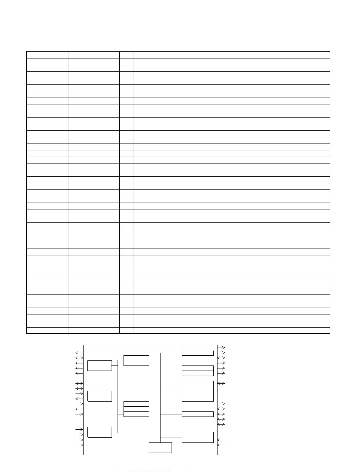
Block Diagram for MPEG1 Video/Audio Processing
RAS#
Processor LA(17:0) DRAM Interface DA(8:0)
Interface LD(7:0)
Huffman
DBUS(15:1)
LCS3#, LCS#(1:0)
RISC
Decoder
DOU# DRAM
LWR#
Processor
2Kx32 ROM
DWE#
LOE#
2x32 SRAM CAS#
ACLK AUX(7:1)
AUX
Serial
ATCLK
MPEG
Audio
AIN
Serial Audio
Processor
Interface
AOUT
Interface
ARFS 64x32 ROM YUV(7:0)
ATFS
32x32 SRAM PCLK2X Screen
ARCLK Registers Video Output PCLK
VSYNC
HSYNC
TDM SEL
-
PLL(1:0)
TDM
Interface
TDMCLK
Interface
On Screen
TDMDR Display CPUCLK Misc
TDMFS
DRAM DMA
RESET#
Controller
CIRCUIT DESCRIPTION
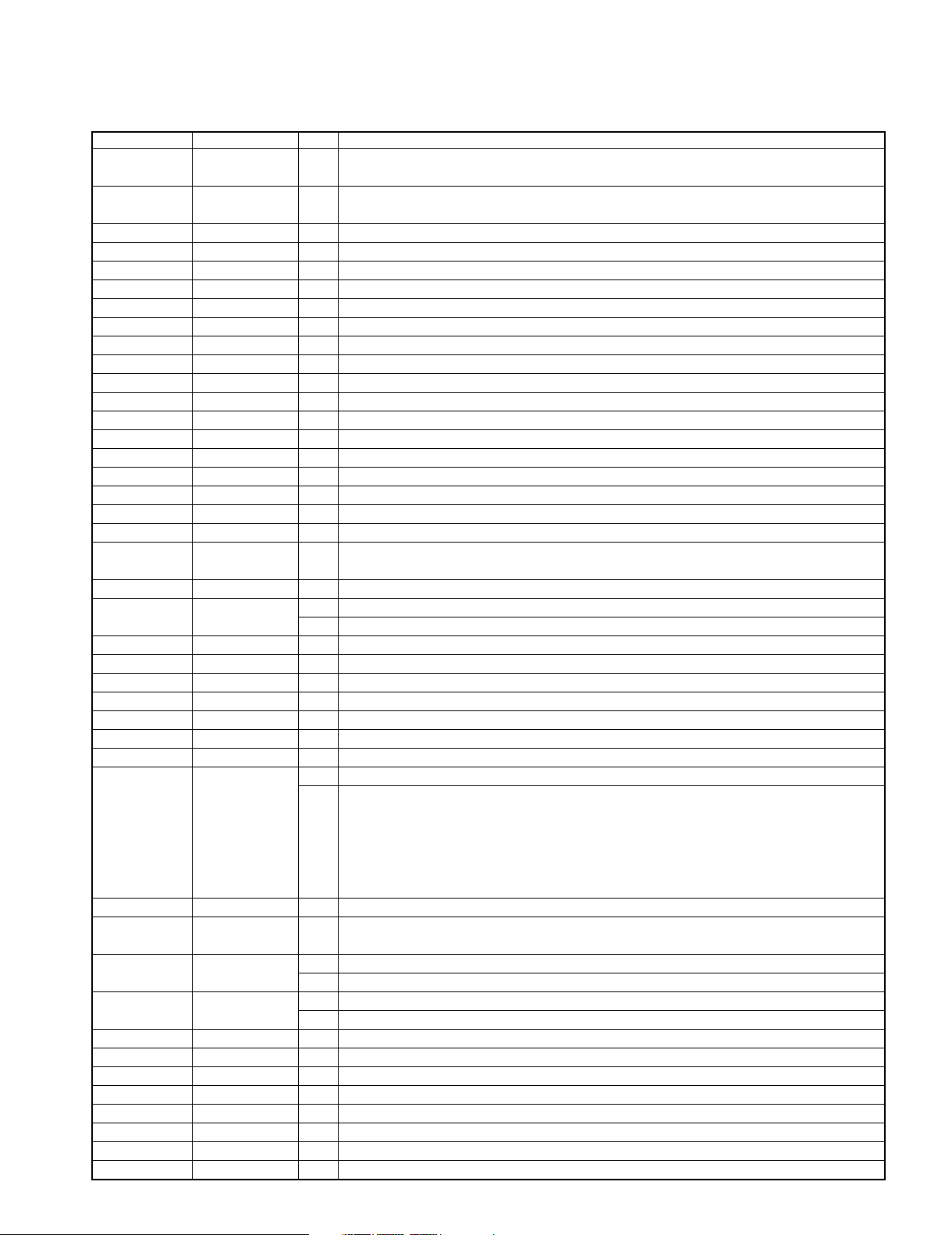
Port Function of MPEG1 Video/Audio Processing : ES3880 (ICM2)
Port No. Port Name I/O Function
1,31,51 VCC3 - Supply voltage for 3.3V.
2 RAS# O DRAM row address strobe (active low).
3 DWE# O DRAM write enable (active low).
4~12 MA(0~8) O DRAM multiplexed row and column address bus.
13~28 DBUS(0~15) I/O DRAM data bus.
29 RESET# I System reset (active low).
30,50,80,100 GND - Ground.
32~39 YUV(0~7) O
40 VSYNC I/O
41 HSYNC I/O
42 CPUCLK I RISC and system clock input.
43 PCLK2X I/O Pixel clock: two times the actual pixel clock for screen video interface.
44 PCLK I/O Pixel clock qualifier in for screen video interface.
45~49,52,53,54 AUX(0~7) I/O Auxiliary control pins (AUX0 and AUX1are open collectors).
55~62 LD(0~7) I/O RISC interface data bus.
63 LWR# O Unused.
64 LOE# O RISC interface output enable (active low).
65,66,67 LCS(3,1,0)# O RISC interface chip select (active low).
68~79,82~87 LA(0~17) O RISC interface address bus.
81 VCC - Digital supply voltage for 5.0V.
88 ACLK I/O
89 AOUT/SEL/PLL0 I CPUCLK for the Visba : 00 = bypass PLL 01 = 54MHz PLL
90 ATCLK I/O Audio transmit bit clock.
91 ATFS/SEL/PLL1 I
92 DOE O
93 AIN I Audio interface serial data input.
94 ARCLK I Audio receive bit clock.
95 ARFS I Audio interface receive frame sync.
96 TDMCLK I TDM interface serial clock.
97 TDMDR I TDM interface serial data receive.
98 TDMFS I TDM interface frame sync.
99 CAS# O DRAM column address strobe bank 0 (active low).
Y is luminance, UV are chrominance data bus for screen video interface.
YUV(0~7) for 8 bit YUV mode.
Vertical sync for screen video interface, programmable for rising or
falling edge.
Horizontal sync for screen video interface, programmable for rising or
falling edge.
Master clock for external audio DAC(8.192MHz, 11.2896MHz, 12.288MHz,
16.9344MHz, and 18.432MHz).
O Dual-purpose pin. AOUT is the audio interface serial data output.
Pins SEL -PLL(1: 0) select phase-lock loop(PLL) clock frequency
10 = 67.5MHz PLL 11 = 81MHz PLL
O Dual-purpose pin. ATFS is the audio interface transmit frame sync.
Pins SEL -PLL(1: 0) select phase-lock loop(PLL) clock frequency CPUCLK
for the Visba. See the SEL -PLL0 pin above for the settings.
Dual-purpose pin. DRAM output enable (active low)/DRAM multiplexed
row and column address bus.
4
RXD-V252/V252-H
CIRCUIT DESCRIPTION
Port Function of DAC & TV Encoder : ES3889 (ICM3)
Port No. Port Name I/O Function
1,25,26,31,72
75,77,91,100
5,16,32,66
73, 78,90
6 DSC C I Clock for programming to access internal registers.
7 AUX0 I/O Unused.
9 AUX1 I/O Servo reverse or control pin.
11 AUX2 I/O Servo LD ON or control pin.
70 AUX3 I/O Unused.
69 AUX4 I/O Servo CCW/Close or control pin.
68 AUX5 I/O Unused.
67 AUX6 I/O Servo XLAT or control pin/VFD DO.
14 AUX7 I/O Servo BRKM/Sense or control pin/VFD DI.
18 AUX8 I/O Servo Mute/Open or control pin/VFD CLK.
20 AUX9 I/O Servo SQS0 or control pin.
34 AUX10 I/O Unused.
35 AUX11 I/O Unused.
36 AUX12 I/O Unused.
38 AUX13 I/O Serial interrupt/CD Mute or control pin.
39 AUX14 I/O Unused.
40 AUX15 I/O Unused.
8,81,83,85
93,95,97,99
10 DSC S I Strobe for programming to access internal registers.
12 DCLK O Dual purpose pin. DCLK is the MPEG decoder clock.
13 RESET B I Video reset (active low).
15 MUTE O Audio mute.
17 MCLK I Audio master clock.
19 TWS I Dual purpose pin. TWS is the transmit audio frame sync.
21 TSD I Transmit audio data input.
22 TBCK I Transmit audio bit clock.
23 RWS
24 RSTOUT B O Reset output (active low).
2~4,27~30
76
33
37 RBCK O Dual purpose pin. RBCK is the receive audio bit clock.
41,51 AGND I Audio analog ground.
42 VCM I ADC common mode reference (CMR) buffer output.
43 VREFP I DAC and ADC maximum reference.
44 VCCAA I Analog VCC(5V).
45,46 AOR+, AOR- O Right channel output.
47,48 AOL-, AOL+ O Left channel output.
49 MIC1 I Microphone input 1.
50 MIC2 I Microphone input 2.
VSS I Ground.
VCC I Supply voltage for 5.0v.
DSC D(7~0) I/O Data for programming to access internal registers.
EXT CLK I EXT CLK is the external clock EXT CLK is an input during bypass PLL mode.
SPLL OUT O SPLL OUT is the select PLL output.
O Dual purpose pin. RWS is the receive audio frame sync.
Pins SEL PLL (1,0) select the PLL clock frequency for the DCLK output.
SEL PLL1 SEL PLL0 DCLK
SEL PLL1
NC - Unused.
RSD O Dual purpose pin. RSD is the receive audio data input.
SEL PLL0 I SEL PLL0 along with SEL PLL1 select the PLL clock frequency for the DCLK output.
SER IN I SER IN is the serial input DSC mode.
I 0 0 Bypass PLL (input mode)
0 1 27MHz (output mode)
1 0 32.4MHz (output mode)
1 1 40.5MHz (output mode)
5
RXD-V252/V252-H
CIRCUIT DESCRIPTION
Port No. Port Name I/O Function
52 VREF I Internal resistor divider generators common mode reference(CMR) voltage.
53 VREFM I DAC and ADC minimum reference.
54 RSET I Full scale DAC current adjustment.
55 COMP I Compensation pin.
56,57,62,63 VGND I Video analog ground.
58 CDAC O Modulated chrominance output.
59,60 VVDD I Video VCC(5V).
61 YDAC O Y luminance data bus for screen video port.
64 VDAC O Composite video output.
65 ACAP I Audio CAP.
71 XOUT O Crystal output.
74 XIN I 27MHz crystal input.
79 PCLK I/O 13.5MHz pixel clock.
80 2XPCLK I/O 27MHz (2 times pixel clock).
82 HSYN B O Horizontal sync (active low).
84 VSYN B O Vertical sync (active low).
86~89,92
94,96,98
YUV(7~0) I YUV data bus for screen video port.
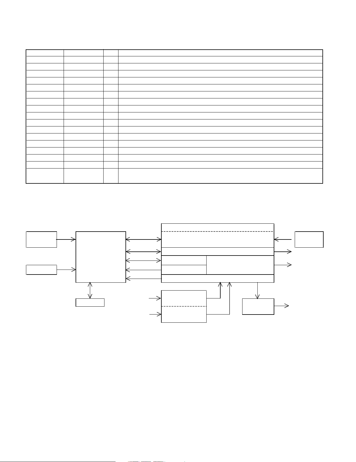
Block Diagram for DAC & TV Encoder : ES3889 (ICM3)
CD-ROM Controller
CD-ROM
Kit
Visba ES3880 Audio DAC Speakers
(Video CD)
ROM PLL
DRAM
Mic 1
Mic 2
Remote Interrupt Remote
Control Control Receiver
Echo/Surround/Vocal Assist
Volume Control
Volume Control
Visba ES3889
Companion Chip
DSC
Pre amp
Pre amp
NTSC/PAL Video
Television
VFD VFD
Driver Panel
6
RXD-V252/V252-H
APPLY WAX AFTER
ADJUST L312
T306
T303
T302
IC301
L354
T351
T301
L312
IC303
IC302
X352
TO ANTENA TERMINAL
75 Ω
75 Ω
37.5 Ω
S.G
(50 Ω )
(50 Ω )
(50 Ω )
TO GND
TO GND
* CENTER FREQ. MARKER 10.7MHz
* CFM GOOD AND MAX 'S'
CURVE IS OBTAINED.
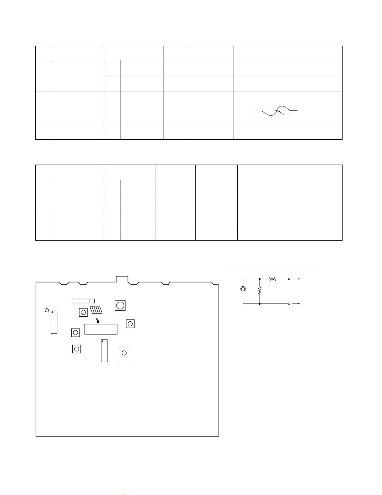
ADJUSTMENT
NO. CHECKING ITEM SG 'N' SET FREQ
1.
FM FREQ (TP301) GIVEN SPEC
COVERAGE
FL 87.5MHz
FH 108.0MHz (TP301) 7.8V ± 0.8V
2. FM IF - 10.7MHz
3.
FM FREQ.
TRACKING (TP302) WAVEFORM APPEAR.
- 98MHz
CONDITION : AM MOD 30% DEV 400Hz
NO. CHECKING ITEM SG 'N' SET FREQ
1.
AM FREQ (TP301) IS WITHIN GIVEN SPEC.
COVERAGE
2. AM IF FL
3.
AM FREQ.
TRACKING (50dB) (ADJUST IF 'NG')
FL 531KHz
FH 1602KHz (TP301) 8.8V ± 0.5V
990KHz T351
(50dB) (TP302) POINT FROM AC VOLTMETER
FL
990KHz
ADJ
POINT
T301
T302
(TP302)
L312
SPEC REMARKS
1.3V ± 0.1V
-
-
ADJ DC VOLTAGE
POINT SPEC
T306
1.1V ± 0.1V
-
TP302
-
ADJUST UNTIL VOLTAGE IS WITHIN
CONFIRM VOLTAGE IS WITHIN
GIVEN SPEC.
ADJUST COIL T302 UNTIL MAX.
OUTPUT
ADJUST L312 UNTIL MAXIMUM
REMARKS
ADJUST UNTIL VOLTAGE
CONFIRM VOLTAGE IS WITHIN
GIVEN SPEC
SP OUTPUT
ADJ T351 UNTIL MAX
î
CONFIRM MAX. OUTPUT.
Adjustment Parts Configuration
ANT DUMMY CIRCUIT FOR FM
7
8
CNS701
BI2
JK601
FW951A
CNP11
CNP1
CNP701
WT902
CNPK1
CNP403
HEADPHONES
JK1
CNS702
CNP102
CNP101CNS101
CNS102
CNP102
SO801
AC801
T801
CNP901
BI901
CNP905
BI11
BI905
CNP2
MOTOR
FAN
M901
CNS902
M
CNP12
BI8
FW701 AFW701 B
DISC
SKIP CLOSE
OPEN/
SW721SW720
FL701
BI606
CNP2
JK671
OUT
VIDEO
CNP9
CNP10
CNP3CNP3A
CNP302AM
FM
SW601
Lch 1
AUX IN
Rch 2
SO401
Rch
GND
GND
SO901
Lch
SP
6 ohm
SO301A
ANTENNA
20
1
18
20
1
15
18
1
6
FFC
51110
110
7
10
1
1
3
1
7
3
1
1
1
10
FFC
TF801
150 C
113
13 1
6
1
1
6
16
1
2
1
2
19
19
11
33
1
2
1
2
7
11
7
1
8
1
8
11
66
2
1
100kHz50kHz
10kHz9kHz
2
1
SECTION
DISPLAY
MIC
SECTION
RXD-V252
SECTION
TUNER/MAIN/POWER
CD/VCD/MP3
SECTION
PICKUP UNIT
PWB-D
MECHA
TAPE
POWER
SECTION
POWER
SECTION
CD MOTOR
RXD-V252/V252-H
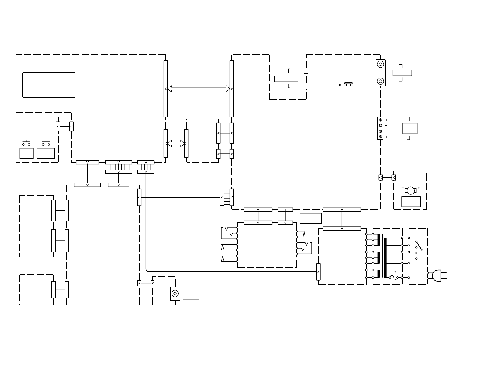
WIRING DIAGRAM
 Loading...