

Page 1
70%
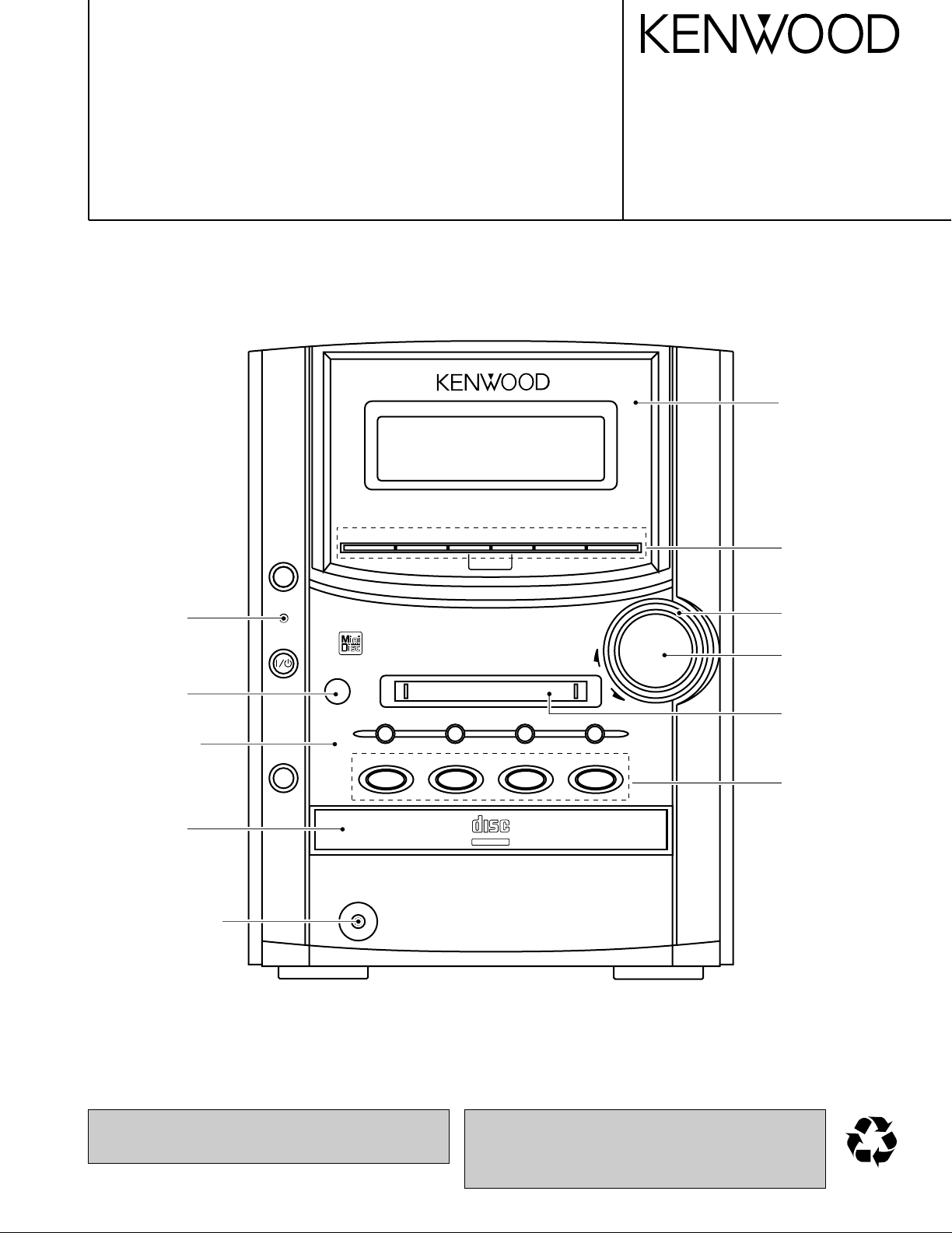
MICRO HiFi COMPONENT SYSTEM
down
standby
/
timer
TAPE
CD
0
0
AUTO REVERSE CASSETTE DECK
HM-382MD
phones
CD
6
MD
6
TAPE
2 3
STOP
volume/
multi control
7
0
MD MD rec TAPE rec TUNER/band
up
AUX sound 4¢menu set/demo
DIGITAL AUDIO
COMPACT
RXD-M32MD
SERVICE MANUAL
(HM-382MD)
© 2000-5/B51-5620-00 (K/K) 2335
Front glass
(B10-3591-08)
Indicator
(B12-0396-08)
Indicator
(B12-0397-08)
Dressing panel *
(A21-)
Panel
(A29-1099-08)
Miniature phone jack
(E11-0200-05)
COMPACT
DIGITAL AUDIO
TEXT
Knob
(K29-7780-08)
Escutcheon
(B07-2517-08)
Knob
(K29-7789-08)
Panel
(A29-1097-08)
Knob *
(K29-)
In compliance with Federal Regulations, following are reproductions of labels on, or inside the product relating to laser
product safety.
* Refer to parts list on page 46.
KENWOOD-Crop. certifies this equipment conforms to DHHS
Regulations No. 21 DFR 1040. 10, Chapter 1, Subchapter J.
DANGER : Laser radiation when open and interlock defeated.
AVOID DIRECT EXPOSURE TO BEAM
Page 2
FM
(T90-0861-05)
indoor antenna (1)
AM
(T90-0852-05)
loop antenna (1)
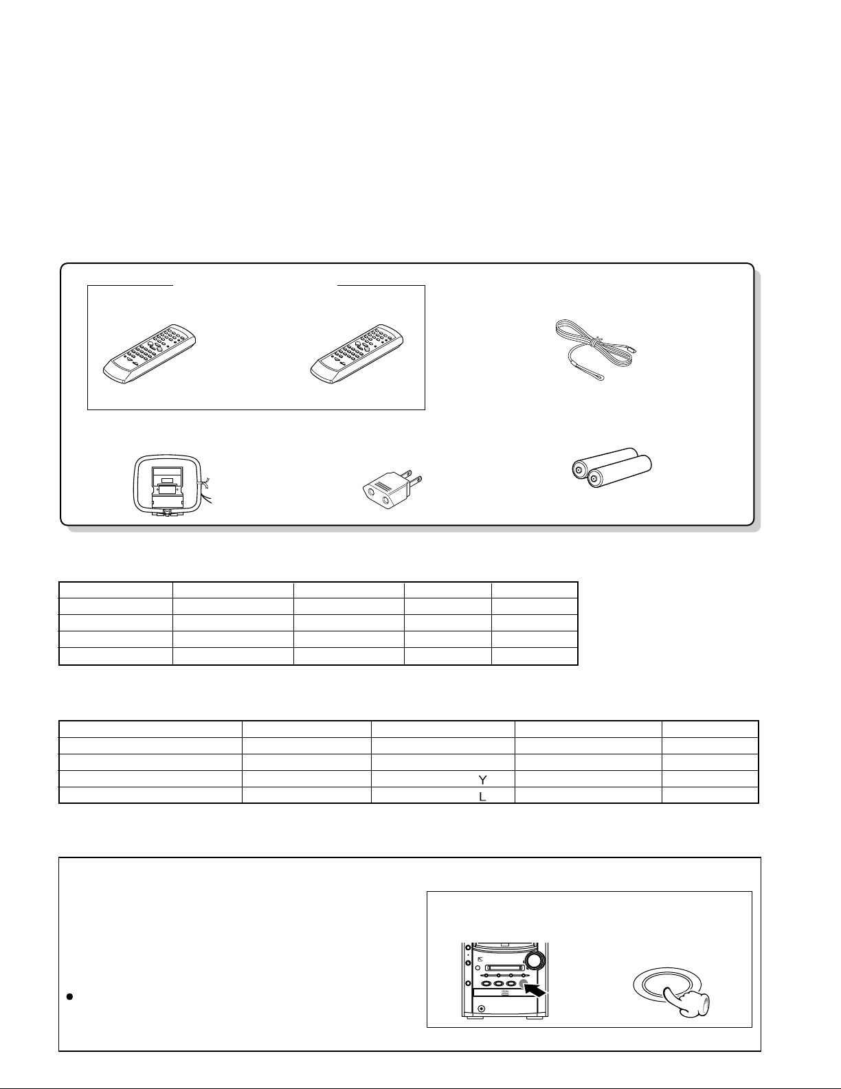
Remote control unit (1)
Batteries AC plug adaptor (1)
(E03-0115-05)
(R6/AA) (2)
Europe
Battery cover(A09-1161-08)
and U.K Other countries
RXD-M32MD
Operation to reset
The microcomputer may fall into malfunction (impossibility to operate, erroneous display, etc.) when the power
cord is unplugged while unit is ON or due to an external
factor. In this case, execute the following procedure to
reset the microcomputer and return it to normal condition.
Unplug the power cord from the power outlet then,
while holding the set/demo key depressed, plug
the power cord again.
Please note that resetting the microcomputer clears
the contents stored in and it returns to condition when
it left the factory.
down
standby
/
timer
TAPE
CD
0
0
SH-3MD
phones
CD6MD6TAPE
2 3
STOP
volume/
multi control
7
STOP
7
0
MD MD rec TAPE rec TUNER/band
up
TEXT
DIGITAL AUDIO
COMPACT
CONTENTS / ACCESSORIES / CAUTIONS
Contents
CONTENTS / ACCESSORIES / CAUTIONS............. 2
EXTERNAL VIEW.......................................................3
DISASSEMBLY FOR REPAIR....................................3
CIRCUIT DESCRIPTION............................................3
ADJUSTMENT..........................................................15
Accessories
PC BOARD .............................................................. 18
SCHEMATIC DIAGRAM...........................................25
EXPLODED VIEW ....................................................43
PARTS LIST..............................................................46
SPECIFICATIONS ......................................Back cover
System configuration
SYSTEM MAIN UNIT DESTINATION SPEAKER COLOR
HM-382MD-L RXD-M32MD-L HMX(L) LS-M32-L BLUE
HM-382MD-S RXD-M32MD-S ETHM(S) LS-M32-S SILVER
HM-382MD-Y RXD-M32MD-Y M1(Y) LS-M32-Y YELLOW
HM-382MD-LS RXD-M32MD-LS HMX(LS) LS-M32-LS SKY • BLUE
Remocon configuration
REMOTE CONTROLLER MODEL NAME MODEL DESTINATIONS COLOR
A70-1375-08 RC-M0100 RXD-M32MD-S M(S) WHITE
A70-1376-08 RC-M0100E RXD-M32MD-S/L THE WHITE
A70-1393-08 RC-M0100 RXD-M32MD- M1(Y) YELLOW
A70-1416-08 RC-M0100 RXD-M32MD-
Cautions
2
MX(L, LS) BLUE
COMPACT
DIGITAL AUDIO
TEXT
Page 3
RXD-M32MD
L
R
AUX
IN
SPEAKERS(6–16Ω)
GND
AM
ANTENNA
FM
75Ω
+
-
LR
FRONT
CAM
CAM
EXTERNAL VIEW
Pin jack
(E63-0095-05)
Side plate R *
(A50-)
Cover *
(F07-)
Top plate
(A52-0387-08)
Side plate L *
(A50-)
Lock terminal board
(E70-0052-05) or
(E20-0321-05)
Lock terminal board
(E70-0053-05)
DISASSEMBLY FOR REPAIR
How to open the tray if not comes out.
(1) From the bottom side of the CD mechanism, use a
screw driver or the like to turn the cam slightly counterclockwise.
(2) Pull out the tray front wards by hand when the tray
comes just out.
AC power cord bushing
(J42-0083-05)
AC power cord *
(E30-)
* Refer to parts list on page 46.
3
Page 4
RXD-M32MD
AVdd
R291
100k‰
R292
U-COM
95pin
(TYPE)
CIRCUIT DESCRIPTION
1. Initialization
1-1 Setting of the Initial Conditions
While pressing the (STOP) key, plug the AC cord to AC
wall outlet.
1-2 Initializing Operation
A microcomputer is initialized for start when the AC
power is turned on while pressing the [STOP] key.
At that time, CD,MD and CASSETTE mechanisms are
also initialized.
During the initial conditions, the display shows "INI-
TIALIZE" and after that it will be returned to standby
conditions.
1-3 Initial Items
ITEMS STATE REMARKS
POWER OFF
BACK LIGHT High
VOLUME 10
BALANCE CENTER
AMP BASS 0
TREBLE 0
EX.BASS ON
LOUDNESS OFF
INPUT SEL TUNER
INPUT LEVEL 0
BAND FM
LAST freq. LOWEST FREQ.
TUNER LAST Preset - -
Channel
AUTO/MONO AUTO
Preset Channel TEST FREQ.
CLOCK AM 12:00 E,T type 24H
PROG ON AM 12:00 E,T type 24H
(TIME)
CLOCK PROG OFF AM 12:00 E,T type 24H
TIMER (TIME)
SOURCE TUNER
Preset Channel 1
EXE MODE OFF
OTT MODE OFF AM 7:00
ASP OFF
SLEEP OFF
DIRECTION FORWARD
DECK TAPE EQ OFF
CD RANDOM OFF
MD REPEAT OFF NONE
1-4 Mechanism Initialization
1-4-1 CD Mechanism
1-4-2 DECK mechanism
4
RVS MODE REVERSE
OPERATION STOP
MODE
PLAY MODE TRACK
REPEAT OFF
OPERATION STOP
MODE
PLAY MODE TRACK NONE
RANDOM OFF NONE
OPERATION STOP NONE
MODE
If a mechanism error occurs, "C" is indicated on the dis-
play.
When the initial condition becomes NG for the third
time, decide the error.
The error condition is displayed as "X" on the display.
1-4-3 MD mechanism
If a mechanism error occurs, "M" is indicated on the
display.
MD disc is ejected from MD mechanism.
1-4-4 If mechanisms (CD/DECK/MD) error occur, the display
is indicated as follows.
C
M X S ERR
1-4-5 TAPE door switch diagnosis
If switches (open/close) error occur, "S" is indicated on
the display.
2. Destination List of Tuner
Set Type BAND
JJ
K,P K1
K2
M,Y
E1
XE1
E1 FM 87.5MHz~108.0MHz 50kHz +10.7MHz 25kHz
E,T
RDS AM 531kHz~1602kHz 9kHz +450kHz 9kHz
2-1 Discrimination Port for Destination
TYPE R292 [Ω] VOLTAGE [V]
J 910k 4.505
K 220k 3.438
M1 100k 2.500
X 47k 1.600
E,T 12k 0.536
AVdd = 5.0 [v]
Receiving Frequency Channel
Range Space
FM 76.0MHz~90.0MHz 100kHz -10.7MHz 25kHz
AM 531kHz~1629kHz 9kHz +450Khz 9kHz
FM 87.5MHz~108.0MHz 100kHz +10.7MHz 25kHz
AM 530kHz~1700kHz 10kHz +450kHz 10kHz
FM 87.5MHz~108.0MHz 100kHz +10.7MHz 25kHz
AM 530kHz~1610kHz 10kHz +450kHz 10kHz
FM 87.5MHz~108.0MHz 50kHz +10.7MHz 25kHz
AM 531kHz~1602kHz 9kHz +450kHz 9kHz
FM 87.5MHz~108.0MHz 50kHz +10.7MHz 25kHz
AM 531kHz~1602kHz 9kHz +450kHz 9kHz
IF RF
3. Test Mode
3-1 Setting of the Test Mode
AUX MODE AUX Key+AC-ON
TUNER MODE TUNER (BAND) Key+AC-ON
TAPE MODE TAPE PLAY Key+AC-ON
CD MODE CD PLAY Key+AC-ON
MD UNIT MODE
MD MECHA. MODE MD REC key +AC-ON
SUB CLOCK OSC
DIAGNOSIS
MD PLAY key + AC ON
(MD version only)
TAPE REC Key+AC-ON
The oscillation diagnosis(existence
of oscillation and measurement of
period) of a sub clock is performed
before the test mode is entered. If
the diagnosis result is OK, the system enters the test mode. If the
diagnosis result is NG, the oscillation of the sub clock is diagnosed
again. If the result is OK, the system enters the test mode. If the
diagnosis result is continuously NG
5 times,the system stops with
"ERR1" and "ERR2" displayed.
Page 5
RXD-M32MD
CIRCUIT DESCRIPTION
3-2 Cancel of the test mode
By turning the power off, the system is initialized and the test mode is canceled.
3-3 Contents of the Test Mode
3-3-1 Tuner Test mode
KEY DISPLAY OPERATION
STOP Normal indication P -- P10 P20 P30 P40
MENU AUTO STEREO ï
Normal indication MANUAL MONO ó
MD REC TUNING DOWN
TAPE REC Normal indication TUNING UP
SKIP DOWN P. ch DOWN
SKIP UP Normal indication P. ch UP
3-3-2 Aux Test Mode
KEY DISPLAY OPERATION
Tone
MAX
SET/demo Tone MAX CENTER MAX MIN
Tone CENTER
SKIP UP Normal indication EX
3-3-3 Deck Test Mode
KEY DISPLAY OPERATION
If the REC/ARM key is pressed, the system record for 4 seconds.
Then, it rewinds to the REC starting position and plays back
TAPE REC Normal display automatically. If the REC/ARM key is pressed, during the
4 seconds REC operation,the system
records further for 4 seconds, then returns to the starting position
of the first 4 seconds REC operation and plays back.
BASS ON LOUDNESS ON SOUND MODE OFF
3-3-4 CD Test Mode
The CD tray is opened automatically when the test mode is entered.
KEY DISPLAY OPERATION
CD-PLAY/PAUSE 05 ✽ ✽ : ✽ ✽
(✽ ✽ : ✽ ✽) Tracking-servo on.
(Change the mode 05 and 03 03 --:-- Tracking-servo off.
alternately by the stop key.)
CD STOP 01 --:-- STOP
Adjustment value/mean value
(Cyclically changed in the 07 ✽ ✽ / ✽ ✽ TB value FB value
stop mode only.) 08 ✽ ✽ / ✽ ✽ TG value FG value
09 ✽ ✽ / ✽ ✽ FE value RF value
10 ✽ ✽ / ✽ ✽ TE value VC value
MENU
SKIP UP Ex.01~02 CD track no. up.
TAPE REC
SKIP DOWN Ex.02~01 CD track no. down.
MD REC
HI-SPEED CD double speed operation
NOR-SPEED CD normal speed operation
CD FF search.
The pickup travels outward in the stop mode.
CD FB search.
The pickup travels inward in the stop mode.
4. MD Test Mode
4-1 MD Unit Mode
Key Display Description
STOP 001—:— Stop the MD operation.
SKIP UP EX : 01-02 MD’s track up operation.
SKIP DOWN EX : 02-01 MD’s track down operation.
SET/demo ALL ERASE Stop the MD operation.
Start operation of all erase if disc is recordable.
5
Page 6
RXD-M32MD
Repair(replace)
Temperature
Standard Set
EEPROM set
value check
Auto pre adj Auto adj Auto Fab adj *EEPROM data write ** Operation check
TEMP EEPROM_SET AUTO_YOBI AUTO_ADJ AUTO_FAB CANCEL TEST MODE TEST-PLAY TEST-REC
pickup - 1 2 3 4 5 6 7
recording head - - - - - - - 1
mechanism - 1 2 3 4 5 6 7
pcb parts 1 2 3 4 5 6 7 8
MD microprocessor - 1 - - - 2 3 4
MD LSI - - 1 2 3 4 5 6
RF IC 1 2 3 4 5 6 7 8
EEPROM 1 2 3 4 5 6 7 8
1-2 Test disc
Type Test disc
1 High reflection disc TGYS1 (SONY)
2 Low reflection disc Recording minidisc
3 Head Adjusting transparent
Entering the specific mode
Whenever the button SKIP DOWN
is pressed, the mode is changed.
AUTO
(AUT YOBI) (AUTO AJST) (AUT FAB) (RST YOBI) (RESULT)
(MNU YOBI)(EEPROM SET) (MNU AJST)
pre-adjustment AUTO adjustment RESULT SUB RESULT
EEPROM setting MANUAL adjustment MANUAL pre-adjustment
AUT
CIRCUIT DESCRIPTION
4-2 MD SECTION
1. Preparation for Adjustment
You have to carry out the following test mode items if replace MD mechanism, pickup, head and pc board.
1-1 Procedure
1. Short-circuit #4(vss) and #7(wp) of IC1402(EEPROM).
2. Set the unit to test mode and carry out the every adjustment in test mode.
3. Stop the test mode by pressing the STOP key for 3 secs
4. Remove the short circuit of IC1402. Carry out reset start.
note: figures order of steps. - = no need.
* Result of EEPROM
OK_EEPROM Write the data of setting values and AUTO-pre adjustment perfectly.
WR_EEPROM Write the data of setting values perfectly however not write AUTO pre-adjustment.
Carry out AUTO-pre adjustment and write data to EEPROM.
NG_EEPROM Not write the data of setting values.
Check the connection of MD microprocessor and EEPROM.
** Carry out the TEST-PLAY , TEST-REC and C1 error in test mode after AUTO_ADJ and AUTO_FAB.
2. Test Mode
1. Holding down the MD rec button and turn the power on. (State
2. To enter the test mode stop state(State B), press the STOP button.
3. Load the playback disc 1(high reflection disc) or recording disc 2(low reflection disc).
A MD TEST
ó (Press STOP key)
B tsm
ó (MD DISC LOAD IN)
C LOADING
ó
D AUT YOBI
6
e ---- TEST MODE STOP STATE represents version of MD microcomputer
(When the STOP button is pressed in the D state, the indication B state is
restored.
To restore D state again, press the SKIP DOWN key once.
A)
Page 7
RXD-M32MD
• Canceling the test mode
When the POWER button is pressed, the test mode is canceled, and the POWER OFF state is set.
• Test Mode
1. AUTO pre-adjustment mode • Automatic pre-adjustment is performed. (After adjustment the grating adjustment mode is set.)
• The adjustment value is output with the aid of system controller interface.
2. AUTO adjustment mode • Automatic adjustment is performed.
• The adjustment value is output with the aid of system controller interface.
• Continuous playback is performed. (Error rate indication, jump test)
4. RESULT sub-mode • The measurement value, set value and calculated value are indicated.
• The set value is changed manually (in servo OFF state).
3. AUTO FOCUS BIAS adjustment • Focus bias adjustment is performed auto matically.
5. RESULT mode (final adjustment) • The set value (after calculation) is indicated.
• The set value is changed manually (in servo OFF state).
6. MANUAL pre-adjustment mode • RF side manual adjustment is performed.
• Focus and tracking signal ATT manual adjustment is performed.
• Focus and tracking signal offset setting is performed.
7. MANUAL adjustment mode • Focus and tracking signal ATT manual adjustment is performed.
8. EEPROM setting mode • EEPROM setting
9. TEST-PLAY mode • Continuous playback from the specified address is performed.
• C1 error rate measurement.
10. TEST-REC mode • Continuous recording from the specified address is performed.
• Change of record laser output (servo gain is also changed according to laser output)
11. EJECT mode • TEMP setting (of EEPROM setting)
1. AUTO pre-adjustment mode (Low reflection disc only)
Step No.
Setting Method
Remarks Display
Step 1 Test mode STOP state [ t s m e ]
Step 2
Press once the SKIP DOWN( ) button.
AUTO pre-adjustment menu [ AUT_ YOBI_ _ _ ]
Step 3 Press once the MD PLAY button. The slide moves to the innermost periphery, and automatic [ : _ _ _ _ _ _ _ ]
pre-adjustment is started.
During automatic adjustment changes as follows.
HAo RFg SAg SBg PTG PCH GTG GCH RCG
SEG RFG SAG HAO HEO TCO LAO
End of adjustment If adjustment is OK, Step 4.
If adjustment is NG, Step 5.
Step 4 Grating adjustment, [ _ C O M P L E T E _ ]
adjustment value output
Press once the MD STOP button. STEP 2
Step 5 Adjustment value output [ AUT YOBI ]
Press once the MD STOP button. STEP 2 AUTO pre-adjustment menu
: Adjustment name, : Address
2. AUTO adjustment mode
Step No.
Setting Method
Remarks Display
Step 1 Test mode STOP state [ t s m e ]
Step 2
Press the SKIP DOWN( ) button two times.
AUTO adjustment menu [ A U T O _ A J S T _ ]
Step 3 Press once the MD PLAY button. The slide moves to the innermost periphery, and automatic [ : _ _ _ _ _ _ ]
adjustment is started.
In case of high reflection disc changes as follows.
PEG
HAG
case of low reflection disc changes as follows.
PEG LAG GCG GEG LAG
End of adjustment If adjustment is OK, Step 4.
If adjustment is NG, Step 7.
Step 4 Adjustment value output
[ C O M P L E T E ]
Press the MD PLAY button. STEP 5
Press the MD STOP button. STEP 2
Step 5
Continuous playback (groove section)
[ a c ]
Step 6
Press the MD STOP button. STEP 2 AUTO adjustment menu
Step 7 Adjustment value output [ C a n ' t _ A D J . ]
Press the MD STOP button. STEP 2 AUTO adjustment menu
: Adjustment name, : Measurement value, : Address
CIRCUIT DESCRIPTION
7
Page 8
RXD-M32MD
3. AUTO FAB adjusting mode
Step No. Setting Method Remarks Display
Step 1 Test mode STOP state
Step 2
Press the SKIP DOWN( ) button three times
AUTO FAB adjustment menu [_AUT_FAB_ _]
Step 3 Press the MD PLAY button 1 time
Step 4 Press the MD STOP button AUTO FAB adjustment menu, step 2
Step 5
• : measurement value : FAB value in measurement, : C1 error value in measurement, : FAB
value
• If the STOP button is pressed twice while the AUTO FAB adjustment is displayed, the state is change to the TEST mode
STOP state.
Step 1 Test mode STOP state [ t s m e ]
Step 2
Press the SKIP DOWN(4) button 4 times.
RESULT sub-menu [ _ R S T _ Y O B I _ ]
Step 3 Press once the MD PLAY button. Indication of measurement value [ R F G : _ _ __ _ ]
Step 4
Press once the SKIP DOWN(4) button.
Indication of measurement value [ R C G : _ _ __ _ ]
Step 5
Press once the SKIP DOWN(4) button.
Indication of measurement value [ P T G : _ _ _ _ _ ]
Step 6
Press once the SKIP DOWN(4) button.
Indication of measurement value [ G T G : _ _ _ _ _ ]
Step 7
Press once the SKIP DOWN(4) button.
Indication of measurement value [ P C H : _ _ _ _ ]
Step 8
Press once the SKIP DOWN(4) button.
Indication of measurement value [ G C H : _ _ _ _ ]
Step 9
Press once the SKIP DOWN(4) button.
Indication of measurement value [ S A G : _ _ _ ]
Step 10
Press once the SKIP DOWN(4) button.
Indication of measurement value [ S B G : _ _ _ ]
Step 11
Press once the SKIP DOWN(4) button.
Indication of measurement value [ S E G : _ _ _ ]
Step 12
Press once the SKIP DOWN(4) button.
Indication of measurement value [ S F G : _ _ _ ]
Step 13
Press once the SKIP DOWN(4) button.
Indication of measurement value [ H A O : _ _ _]
Step 14
Press once the SKIP DOWN(4) button.
Indication of measurement value [ H B O : _ _ _]
Step 15
Press once the SKIP DOWN(4) button.
Indication of measurement value [ H E O : _ _ _]
Step 16
Press once the SKIP DOWN(4) button.
Indication of measurement value [ H F O : _ _ _]
Step 17
Press once the SKIP DOWN(4) button.
Indication of measurement value [ L A O : _ _ _]
Step 18
Press once the SKIP DOWN(4) button.
Indication of measurement value [ L B O : _ _ _]
Step 19
Press once the SKIP DOWN(4) button.
Indication of measurement value [ L E O : _ _ _]
Step 20
Press once the SKIP DOWN(4) button.
Indication of measurement value [ L F O : _ _ _]
Step 21
Press once the SKIP DOWN(4) button.
Indication of measurement value [ T C O : _ _ _ _]
Step 22
Press once the SKIP DOWN(4) button.
Indication of adjustment error sequence No. [ Y O B : _ _ _ _]
Step 23
Press once the SKIP DOWN(4) button.
Indication of adjustment status [ D I F : _ _ _ _]
Step 24
Press once the SKIP DOWN(4) button.
Indication of pre-adjustment not completed (00)/completed (4B) [ A D J : _ _ _ _]
Step 25 Press once the MD STOP button. RESULT sub-menu state [ _ R S T _ Y O B I _ ]
4. RESULT sub-mode
Step No.
Setting Method
Remarks Display
: Measurement value, : Adjustment value, : Other various informations
When the (¡)button in remote controller is pressed while the setting is displayed, the setting increases,
and a new setting is stored in RAM.
When the (1)button in remote controller is pressed while the setting is displayed, the setting increases,
and a new setting is stored in RAM.
When the (¡) or (1)button in remote controller is pressed continously, steps is change by 100ms period.
CIRCUIT DESCRIPTION
End of automatic adj. step 4
High reflection disc step 5
Message output for 1 sec. AUTO FAB.
Adjustment menu(high reflection disc)
8
Page 9
RXD-M32MD
When the (¡)button in remote controller is pressed while the setting is displayed, the setting increases,
and a new setting is stored in RAM.
When the (1)button in remote controller is pressed while the setting is displayed, the setting increases,
and a new setting is stored in RAM.
When the (¡) or (1)button in remote controller is pressed continously, steps is change by 100ms period.
Step 1 Test mode STOP state [ t s m e ]
Step 2
Press the SKIP DOWN(4) button 5 times.
RESULT menu [ _ R S T U L T _ _ _ ]
Step 3 Press once the MD PLAY button. Indication of set value [ H A G : _ _ _ ]
Step 4
Press once the SKIP DOWN(4) button.
Indication of set value [ H B G : _ _ _ ]
Step 5
Press once the SKIP DOWN(4) button.
Indication of set value [ L A G : _ _ _ ]
Step 6
Press once the SKIP DOWN(4) button.
Indication of set value [ L B G : _ _ _ ]
Step 7
Press once the SKIP DOWN(4) button.
Indication of set value [ P E G : _ _ _ ]
Step 8
Press once the SKIP DOWN(4) button.
Indication of set value [ P F G : _ _ _ ]
Step 9
Press once the SKIP DOWN(4) button.
Indication of set value [ G E G : _ _ _ ]
Step 10
Press once the SKIP DOWN(4) button.
Indication of set value [ G F G : _ _ _ ]
Step 11
Press once the SKIP DOWN(4) button.
Indication of set value [ G C G : _ _ _ _ ]
Step 12 Press once the MD STOP button. RESULT menu state [ _ R E S U L T _ _ _ ]
5. RESULT mode (final adjustment)
Step No.
Setting Method
Remarks Display
: Measurement value
Step 1 Test mode STOP state [ t s m e ]
Step 2
Press the SKIP DOWN(4) button 6 times.
MANUAL auxiliary adjustment mode [ _ M N U _ Y O B I _ ]
Step 3 Press once the MD PLAY button. Initial setting Temperature measuring mode [ T M P : _ _ _ _ ]
Step 4
Press once the SKIP DOWN(4) button.
Offset "0" setting A signal offset tentative measurement [ H A o : _ _ _ ]
Step 5
Press once the SKIP DOWN(4) button.
B signal offset tentative measurement [ H B o : _ _ _ ]
Step 6
Press once the SKIP DOWN(4) button.
E signal offset tentative measurement [ H E o : _ _ _ ]
Step 7
Press once the SKIP DOWN(4) button.
F signal offset tentative measurement [ H F o : _ _ _ ]
Step 8
Press once the SKIP DOWN(4) button.
Offset tentative measurement Laser ON [ L O N : _ _ _ _ _ _ ]
Step 9
Press once the SKIP DOWN(4) button.
Innermost periphery move RF side FG rough adjustment [ R F g : _ _ ]
Step 10
Press once the SKIP DOWN(4) button.
Focus ATT (A signal) tentative setting [ S A g : ]
Step 11
Press once the SKIP DOWN(4) button.
Focus ATT (B signal) tentative setting [ S B g : ]
Step 12
Press once the SKIP DOWN(4) button.
RF side pit section TG adjustment [ P T G : _ _ ]
Step 13
Press once the SKIP DOWN(4) button.
Pit section COUT level setting [ P C H : _ ]
Step 14
Press once the SKIP DOWN(4) button.
Outer periphery move RF side groove TG adjustment [ G T G : _ _ ]
Step 15
Press once the SKIP DOWN(4) button.
Groove section COUT level setting [ G C H : _ ]
Step 16
Press once the SKIP DOWN(4) button.
RF side TCRS adjustment [ R C G : _ _ ]
Step 17
Press once the SKIP DOWN(4) button.
Tracking ATT (E signal) setting [ S E G : ]
Step 18
Press once the SKIP DOWN(4) button.
Tracking ATT (F signal) setting [ S F G : ]
Step 19
Press once the SKIP DOWN(4) button.
Indication of tracking EFMIO measurement [ g M I : _ _ _ ]
Step 20
Press once the SKIP DOWN(4) button.
RF side pit section FG adjustment [R F G : _ _ ]
Step 21
Press once the SKIP DOWN(4) button.
Focus ATT (A signal) setting [ S A G : ]
Step 22
Press once the SKIP DOWN(4) button.
Focus ATT (B signal) setting [ S B G : ]
Step 23
Press once the SKIP DOWN(4) button.
Offset "0" setting A signal offset measurement [ H A O : _ _ _ ]
Step 24
Press once the SKIP DOWN(4) button.
B signal offset measurement [ H B O : _ _ _ ]
Step 25
Press once the SKIP DOWN(4) button.
E signal offset measurement [ H E O : _ _ _ ]
Step 26
Press once the SKIP DOWN(4) button.
F signal offset measurement [ H F O : _ _ _ ]
Step 27
Press once the SKIP DOWN(4) button.
TCRS signal offset measurement [ T C O : _ _ _ ]
Step 28
Press once the SKIP DOWN(4) button.
A signal offset measurement [ L A O : _ _ _ ]
Step 29
Press once the SKIP DOWN(4) button.
B signal offset measurement [ L B O : _ _ _ ]
Step 30
Press once the SKIP DOWN(4) button.
E signal offset measurement [ L E O : _ _ _ ]
Step 31
Press once the SKIP DOWN(4) button.
F
Step 32 Press once the MD STOP button. MNU YOBI state
signal offset measurement [ L F O : _ _ _ ]
[_MNU_YOBI_]
6. MANUAL auxiliary adjustment mode (only low reflection disc)
Step No.
Setting Method
Remarks Display
: Measurement value, : Set value, : Account value
CIRCUIT DESCRIPTION
9
Page 10
If the measurement value is within the OK range, " " appears on the 8th character.
Step 1 Test mode STOP state [ t s m e ]
Step 2
Press the SKIP DOWN(4) button 7 times.
MANUAL adjustment menu [ _ M N U _ A J S T _ ]
Step 3 Press once the MD PLAY button. Initial setting Temperature measuring mode [ T M P : _ _ _ _ ]
Step 4
Press once the SKIP DOWN(4) button.
Laser ON [ L O N : _ _ _ _ _ _ ]
Step 5
Press once the SKIP DOWN(4) button.
Innermost periphery move Tracking ATT (E signal) setting [ P E G : ]
Step 6
Press once the SKIP DOWN(4) button.
Tracking ATT (F signal) setting [ P F G : ]
Step 7
Press once the SKIP DOWN(4) button.
Indication of tracking EFMIO measurement [ P M I : _ _ _ ]
Step 8
Press once the SKIP DOWN(4) button.
Focus ATT (A signal) setting [ H A G : ]
Step 9
Press once the SKIP DOWN(4) button.
Focus ATT (B signal) setting [ H B G : ]
7. MANUAL adjustment mode
High reflection disc
Step No.
Setting Method
Remarks Display
If the MD STOP button is pressed twice while the MANUAL adjustment menu is displayed, the state is changed to the TEST
mode STOP state.
When the (¡)button in remote controller is pressed while the setting is displayed, the setting increases,
and a new setting is stored in RAM.
When the (1)button in remote controller is pressed while the setting is displayed, the setting increases,
and a new setting is stored in RAM.
When the (¡) or (1) button in remote controller is pressed continously, steps is change by 100ms period.
8. TEST-PLAY mode
Step 1 Test mode STOP state [ t s m e ]
Step 2
Press once the SOUND button.
[ T E S T _ P L A Y _ ]
Step 4
Press
Step 3
Press the STOP button.
once the MD PLAY button.
During search the search output is set to "H", and it is
returned to "L" when continuous playback is started.
Step 5
Continuous playback (groove section)
(Address + C1 error indication)
[a
c ]
Step 6
Press once the MD STOP button. TEST-PLAY menu [ T E S T _ P L A Y _ ]
[ T E S T _ P L A Y _ ]
Step No.
Setting Method
Remarks Display
If the MD STOP button is pressed while the TEST-PLAY menu is displayed, TEST mode STOP state is set.
If the MD PLAY button is pressed while the TEST-PLAY menu is displayed, continuous playback is started from the current pickup position.
: Adress, : Error late
Step 1 Test mode STOP state [ t s m e ]
Step 2
Press the SKIP DOWN(4) button 7 times.
MANUAL adjustment menu [ _ M N U _ A J S T _ ]
Step 3 Press once the MD PLAY button. Initial setting → Temperature measuring mode [ T M P : _ _ _ _ ]
Step 4
Press once the SKIP DOWN(4) button.
Laser ON [ L O N : _ _ _ _ _ _ ]
Step 5
Press once the SKIP DOWN(4) button.
Innermost periphery move → Tracking ATT (E signal) setting [ P E G : ]
Step 6
Press once the SKIP DOWN(4) button.
Tracking ATT (F signal) setting [ P F G : ]
Step 7
Press once the SKIP DOWN(4) button.
Indication of tracking EFMIO measurement (pit section) [ P M I : _ _ _ ]
Step 8
Press once the SKIP DOWN(4) button.
Focus ATT (A signal) setting [ L A g : ]
Step 9
Press once the SKIP DOWN(4) button.
Focus ATT (B signal) setting [ L B g : ]
Step 10
Press once the SKIP DOWN(4) button.
Outside periphery move → Track closs setting [ G C G : ]
Step 11
Press once the SKIP DOWN(4) button.
Tracking ATT (E signal) setting [ G E G : ]
Step 12
Press once the SKIP DOWN(4) button.
Tracking ATT (F signal) setting [ G F G : ]
Step 13
Press once the SKIP DOWN(4) button.
Indication of tracking EFMIO measurement (groove section) [ G M I : _ _ _ ]
Step 14
Press once the SKIP DOWN(4) button.
Focus ATT (A signal) setting [ L A G : ]
Step 15
Press once the SKIP DOWN(4) button.
Focus ATT (B signal) setting [ L B G : ]
Low reflection disc
Step No.
Setting Method
Remarks Display
If the MD STOP button is pressed twice while the MANUAL adjustment menu is displayed, the state is changed to the TEST mode
STOP state.
RXD-M32MD
CIRCUIT DESCRIPTION
10
Page 11

RXD-M32MD
SOUND button twice.
9. TEST-REC mode
Step 1 Test mode STOP state [ t s m e ]
Step 2
Press the
[ T E S T _ R E C _ _ ]
Step 3 Press the STOP button.
Step 4 Press once the MD PLAY button. During search the search output is set to "H", and it is
(returned on "L" when continuous playback is started.Address +
C1 error indication) Continuous recording [ a
p w ]
[ a
p w ]
Step 5 Press once the MD STOP button. TEST-REC menu [ T E S T _ R E C _ _ ]
[ T E S T _ R E C _ _ ]
Step No.
Setting Method
Remarks Display
If the MD STOP button is pressed while the TEST-PLAY menu is displayed, TEST mode STOP state is set.
If the MD PLAY button is pressed while the TEST-REC menu is displayed, continuous record is started from the current pickup position.
If
: Measurement value, : Setting value.
the (¡) or (1) button in remote controller is pressed in TEST-REC mode and continuous record mode,
the laser record power changes.
(Servo gain changes also according to the record power.)
: Adress, : Laser power cord
10. EJECT mode
Step 2
Step 1
Test mode
Test mode STOP state
EJECT Eject of MD discstate [ _ _ E J E C T _ _ _ ]
Step 3 Press SOUND button. Temperature standard value setting. [ TEMP ]
Step 4 Press STOP button. [ _ _ EJECT _ _ _ _ ]
Step No.
Setting Method
Remarks Display
DISPLAY DESCRIPTION
BLANK DISC Non Recorded disc
CAN’T COPY Inhibit to record by SCMS
CAN’T EDIT Inhibit to edit by MD standard
CAN’T REC Inhibit to record by disc damage(10 or more
defects/recordable cluster is 0)
DISC ERROR**
OR : UTOC read error or FTNO>LTNO
(edit/record) permit ALL ERASE only
DO : Start address TNO>endless TNO
(playback) handle poor TNO as 1SG
(edit/record) permit ALL ERASE only
C0 : Write poor data in UTOC0
C1 : Write poor data in UTOC1
C2 : Write poor data in UTOC2
C4 : Write poor data in UTOC4
(play back) playback even if address
roof(C0)
(edit/record) permit ALL ERASE only
DISC FULL
No recordable area
MECH ERR**
10-13 : head poor down
20-23 : head poor up
no disc No disc in the unit
NO TRACKS Disc recorded title only
NOT AUDIO Disc recorded audio signal.
PLAY ONLY Record to music disc
PROTECTED Record disc inhibited to record
READING In mode of reading TOC or UTOC
SRCH ERR** 30 : Search time over in playback, FF or FB
31 : Search time over in REC-PAUSE
32 : Search time over in record
TEMP OVER High temperature
TITLE FULL Input over letter of title
UNIT ERROR Hardware damage
UTOC W ERR Error of writing to UTOC
WRITING In writing to UTOC
8. MD mechanism error message
Display
Value Voltage
TOC
recording
power
Actual power output
00H 2.50 mW 6E H 1.354 V
01H 2.60 mW 74 H 1.427 V
02H 2.70 mW 7B H 1.513 V
03H 2.85 mW 83 H 1.612 V
04H 3.00 mW 8A H 1.698 V
05H 3.15 mW 93 H 1.809 V
06H 3.30 mW 93 H 1.809 V
07H 3.45 mW 9C H 1.920 V
08H 3.60 mW A6 H 2.043 V
09H 3.75 mW AE H 2.141 V
0AH 3.95 mW B9 H 2.289 V
0BH 4.15 mW B9 H 2.289 V
0CH 4.35 mW C4 H 2.412 V
0DH 4.55 mW CF H 2.547 V
0EH 4.75 mW DB H 2.695 V
0FH 5.00 mW DB H 2.695 V
• POWER
CIRCUIT DESCRIPTION
11
Page 12

SINGLE CD
MECHA.
KSL213CCM
CASSETTE DOOR
MECHA.
A/D KEY
INPUT
TYPE
STANDBY/
TIMER
LED
MUTING
CONTROL
CIRCUIT
CD D.S.P IC
CDX3017Q
X32,IC3
DECK
MECHA
CIRCUIT
AUTO REVERSE
CASSETTE
ADR-2176TR3
DECK CONTROL
CIRCUIT
HA12219NT
M30622MA-1A5FP
M30624MG-307FP
M-COM
TUNER
PLL IC
LC72131
X14,IC2
X29,IC114
X29,IC106
X29,IC105
RDS IC
SAA6579T
X14X29
BACK LIGHT
CIRCUIT
AMP
AUDIO
OUTPUT
CIRCUIT
(MD VERSION ONLY)
LCD MODULE
REMOTE
CONTROL
SELECTOR IC
M62498AFP
MD MECHA UNIT
MDM99D
RXD-M32MD
CIRCUIT DESCRIPTION
5. Main Microprocessor : X29(IC104) M30622MA-1A5FP (DECK VERSION)
M30624MG-307FP (MD VERSION)
5-1 Main Microprocessor Periphery Block Diagram
5-2. Key Matrix
12
INPUT KEY1 KEY2
VOLTAGE(V) Pin90 Pin91
0.00 0.23 TUNER/BAND SET/ DEMO
0.24 0.67 STOP MENU
0.68 1.12 TAPE REC SKIP UP
1.13 1.60 TAPE PLAY (F PLAY) SKIP DOWN
1.61 2.02 MD REC (TAPE O.T.E.) SOUND
2.03 2.74 MD PLAY (R PLAY) AUX
2.75 2.47 MD EJECT (TAPE EQ) -
2.48 3.37 CD PLAY -
3.38 3.82 CD OPEN/CLOSE -
3.83 4.27 POWER -
4.28 4.74 TAPE OPEN/CLOSE -
4.75
5.00 KEY OFF KEY OFF
Vref=5V
( ) Deck version
Page 13

RXD-M32MD
CIRCUIT DESCRIPTION
5-3 Pin Description of Main Microprocessor
Pin No. Pin Name I/O Description
1 CD_PROTECTION I Detection port for CD protection. H = NORMAL L = PROTECTION ON
2 CD_OPEN_SW I CD open detection switch input. H = OFF L = ON
3 CD_OPEN_M O CD tray motor control output (open). H = OFF L = ON
4 CD_CLOSE_M O CD tray motor control output (close). H = OFF L = ON
5 CD_CLOSE_SW I CD close detection switch input. H = ON L = OFF
6 RDS_DATA I RDS data input.
7 CE I Power failure input port. H = AC ON L = AC OFF
8 BYTE I GND.
9 CNVSS I GND.
10 XCIN I Timer clock input (32.768kHz).
11 XCOUT O Timer clock output (32.768kHz).
12 RESET I Reset signal input for microprocessor. H = NORMAL L = RESET
13 XOUT O Main clock oscillator(10MHz).
14 VSS I GND.
15 XIN I Main clock oscillator(10MHz).
16 VCC(B.U) I Power supply(+5.0v).
17 NMI I Connected to VCC.
18 REMOCON I Remote control signal input.
19 RDS_CLK I RDS clock input.
20 SCOR I Sub code synchronized signal input.
21 SCLK O CD sense data read out clock.
22 SENSE I CD sense input.
23 CD_CLK O CD DSP clock output.
24 XLAT O CD DSP latch output. L = LATCH
25 CD_DATA O CD DSP data output.
26 SYSM O CD DSP system mute output.
27 CDRST O CD DSP reset signal output.
28 SQCK O CD sub code clock output.
29 SUBQ I CD sub code input.
30 NC O Unused.
31 K_DATA O MD data output (MD version only).
32 MD_DATA I MD data input (MD version only).
33 MD_SCK O MD clock output (MD version only).
34 LED2 O Control port of standby/timer LED(red). L = ON
35 LCD_DATA O Data output to LCD driver IC.
36 NC O Unused.
37 LCD_CLK O Clock output to LCD driver IC.
38 LED1 O Control port of standby/timer LED (green). L = ON
39 ENC1 I Rotary encoder input (up).
40 ENC2 I Rotary encoder input (down).
41 DECK_CMP O Deck capstan motor control.
42 DECK_SOL O Deck solenoid control.
43 PLAY_SW I Deck play switch input.
44 CrO2_SW I Deck CrO2 detection switch input. H = CrO2 L = Normal
45 PACK_SW I Deck pack switch input. H = OFF L = ON
46 REC_F_SW I Deck forward rec switch input. H = OFF L = ON
47,48 NC - Unused.
49 REC_R_SW I Deck reverse rec switch input. H = OFF L = ON
50 NORMAL_BIAS O Deck bias (Normal/CrO2) change-over.
13
Page 14

RXD-M32MD
CIRCUIT DESCRIPTION
Pin No. Pin Name I/O Description
51 REC/PLAY O Deck rec/play control.
52 BIAS O Deck bias control.
53 120/70 O Deck EQ. control.
54 A/B-1 O Mode selection for deck.
55 A/B-2 O Mode selection for deck.
56 B-1/2 O Mode selection for deck.
57 SD I SD detector input. H = NO TUNED L = TUNED
58 STEREO I Stereo detector input. H = MONO L = STEREO
59 PLL_DATA O PLL IC data output.
60 PLL_DO I PLL IC data input.
61 PLL_CE O PLL IC chip enable.
62 VCC(B.U) I Power supply(+5.0v).
63 PLL_CLK O PLL IC clock output.
64 VSS I GND.
65 VOL_CLK O Clock output to selector IC.
66 VOL_DATA O Data output to selector IC.
67 CLOSE_SW I Close detection switch input for CD door. H = OF F L = ON
68 OPEN_SW I Open detection switch input for CD door. H = OF F L = ON
69 DOOR F O CD door (open) control output. H = ON L = OFF
70 DOOR R O CD door (close) control output. H = ON L = OFF
71 LCD_RST O Reset signal output to LCD driver IC. H = NORMAL L = RESET
72 LCD_CS O CS signal output to LCD driver IC.
73 BACK_LIGHT O Back light control output.
74 SP_RERAY O Speaker relay control output. H = ON L = OFF
75 PROTECTION O Detection input port for protection circuit H = PROTECTION ON
76 H.P SW I Headphones detection input. H = OFF L = ON
77 A_MUTE O Audio muting control output. H = OFF L = ON
78 B.U SW O Unused.
79 DSTB I MD STB input port.
80 SEARCH O MD search output.
81 MD_ST O MD ON/CD sync. output.
82 MD_RST O Reset signal output to MD.
83 LOAD SW I Loading switch input from MD.
84 PDOWN O MD power supply. H = ON L = OFF
85 P.RELAY O Power relay control output. H = ON L = OFF
86 CD_POWER O CD power ON/OFF control. H = NORMAL L = AC OFF
87 CD_MON O CD monitor output. H = ON L = OFF
88 CD_SPEED O Speed control port for CD. H = ON L = OFF
89 M TYPE CE O Unused.
90 KEY1 I A/D key (key1) input port.
91 KEY2 I A/D key (key2) input port.
92 RDS_SLEVEL I RDS Slevel input.
93 MD_BUP(NC) I Detection port for MD back up.
94 PHOTO I Detection port for deck reel pulse.
95 TYPE I Discrimination port for destination.
96 AVSS I GND.
97 CD DIFFECT I Unused.
98 VREF I A/D reference voltage(+5V). (No backed up 5V)
99 AVCC I A/D reference voltage(+5V). (backed up 5V)
100 NC O Unused.
14
Page 15

ADJUSTMENT
CD player adjustment
No.
ITEM
TEST MODE: While pressing the CD PLAY key, turn the power on.
✽
LASER
1
POWER
INPUT
SETTING
–
OUTPUT
SETTING
Set the senor section
of the optical power
meter on the pickup
lens.
PLAYER
SETTING
Press the "PLAY" key
to check that the dis-
play is "03".
RXD-M32MD
ALIGNMENT
POINT
–
ALIGN FOR
On the power
from.0.05 to 0.15mW.
when the diffraction
grating is correctly
aligned with the RF
level of 0.8Vp-p or
more
FIG.
(a)
LASER
2
CURRENT
FOCUS
ERROR
3
BIAS
Note:
Type 4disc :SONY YEDS-18 Test Disc or equivalent. (KTD-02)
LPF : Around 47kΩ + 390pF or so.
Test disc
Type 4
Test disc
Type 4
Connect the DC volt-
meter to CN3 (3, 4)
on X32.
Connect an oscillo-
scope as follows.
CH1: RF(CN3, 1)
GND : VC(CN3, 2)
✽ X32
Press the "PLAY" key
to check that the dis-
play is "03" or "05"
key. Confirm that the
(a) Laser Power
0.05~0.15 mW
Pickup
Optical power meter
Press the "PLAY"
display is "05".
(d)
–
VR 1
RF signal: AC coupled
220mV to 550mV
Optimum eye pattern
(d)
✽ How To Check the Laser Power
1. Set the test mode.
(The CD tray is opened automatically.)
2. To close the CD tray, press the OPEN/CLOSE key.
3. Move the pickup to outward by pressing the TAPE REC key.
¶ RF signal in test mode (PLAY).
¶ Perform the tangential and focusing offset are focused
into one point on the display. The crossing points above
and below the center shall also be looked clearly.
15
Page 16

RXD-M32MD
L
R
AUX
IN
SPEAKERS(6–16Ω)
GND
AM
ANTENNA
FM
75Ω
+
-
LR
AG
{
(A)
(B)
Oscilloscope
AC voltmeter AC voltmeter
Frequency counter
X29 CN3
TEST PIN
1
2
3
4
5
6
7
L-PLAY
L-REC
GND
R-REC
R-PLAY
GND
ERASE
RVS FWD
NO. ITEM
INPUT
SETTING
OUTPUT
SETTING
CASSETTE TAPE
DECK SETTING
ALIGNMENT
POINTS
ALIGN FOR FIG.
Unless otherwise specified, set the respective switches as follows: 0dBs = 0.775V
TAPE : NORMAL
I Cassette mechanism unit (Adjustment of the REC / PLAY head)
(1)
Demagnetization
and cleaning
Power : OFF
Demagnetization,
cleaning, PLAY
Recording
head, erase
head, capstan
pinch roller
Demagnetize the REC / PLAY head
with the head eraser. Clean the REC/
PLAY head, erase head, capstan and
pinch roller using a cotton swab slightly
damped with alcohol.
(2)
Azimuth of the
REC / PLAY
head
SCC-1727
TCC-153
MTT-114
10kHz, -10dB
(B) PLAY
Adjust the output to maximum and
adjust the azimuth adjustment screw
for the Lissajours waveform pattern of
the oscilloscope to become close to a
45ß straight ling.
II PC board adjustment.
(1)
BIAS
CURRENT
(A)
Adjust the AG for the
output of the DECK to
become -20dBs
at 12.5kHz/400Hz.
(AC-224)
(B) REC PLAY
VR101(L)
VR102(R)
Record 400Hz and 12.5kHz alternately,
and adjust the bias current adjustment
potentiometer for the playback levels to
become the same.
Cassette deck adjustment
ADJUSTMENT
16
Page 17

L
R
AUX
IN
SPEAKERS(6–16Ω)
GND
AM
ANTENNA
FM
75Ω
+
-
LR
(A)
(B)
(C)
FM SG
FM SG
AG
MPX AG
AC voltmeter
Dummy antenna
Oscilloscope
Distortion meter
No.
ITEM
INPUT
SETTINGS
OUTPUT
SETTINGS
RECEIVER
SETTINGS
ALIGNMENT
POINTS
ALIGN FOR
FIG.
1 DISCRIMINATOR
(A)
98.0MHz 1kHz,
±40kHz dev.
70dBf (ANT. input)
Connect a
DC voltmeter
between CN4 1
and CN4 2 (X14)
MONO
98.0MHz
L4
(X14-)
0V
2
DISTORTION
(MONO)
(A)
98.0MHz 1kHz,
±40kHz dev. MONO
70dBf (ANT. input)
(B)
MONO
98.0MHz
L5
(X14-)
Minimum
distortion
3
DISTORTION
(STEREO)
(C)
98.0MHz 1kHz,
±40kHz dev.
Selector : L or R Pilot
: ±6kHz dev.
70dBf (ANT. input)
(B)
AUTO
98.0MHz
IFT(RF
FRONTEND
: A1)
(X14-)
Minimum
distortion
(L or R)
4 TUNING LEVEL
(A)
98.0MHz MONO
1kHz, ±40kHz dev.
30dBf (ANT. input)
MONO
98.0MHz
VR1
(X14-)
Adjust VR1
and stop at the
point where ED1
(TUNED) goes
on.
FM SECTION : SELECTOR : FM *Adjust NO.1 and NO.2 repeat.
Tuner adjustment
RXD-M32MD
ADJUSTMENT
SYSTEM CONNECTIONS
17
Page 18

A BDCE
MD MAIN PWB-E (TOP VIEW)
C1602
R1601
R1204
R1203
R1616
C1611
C1612
R1617
C1613
C1615
R1620
R1618
C1607
R1606
C1604
C1603
R1605
XL1201
R1200
R1201
C1207
C1200
L1201
R1202
R1600
C1601
C1619
L1600
C1206
C1119
C1106
R1107
C1109
C1111
C1108
C1105
C1104
C1101
C1102
R1103
C1103
L1200
C1202
R1206
R1207
R1205
R1106
C1112
C1110
L1100
L1101
R1111
R1112
C1117
C1114
R1109
C1115
R1108
C1113
R1110
C1116
C1118
R1444
C1411
R1443
R1435
R1401
C1409
R1212
C1210
C1616
R1622
R1623
R1440
R1420
R1403
D1402
R1424
R1462
R1409
R1405
Q1403
Q1402
Q1802
R1407
Q1803
C1303
IC1300
R1614
R1612
Q1801
D1401
R1801
Q1800
Q1501
C1802
R1806
R1805
Q1805
R1808
Q1806
C1803
C1800
R1304
C1700
C1711
R1711
R1714
C1714
C1501
R1716
C1706
R1802
R1803
C1509
C1506
R1515
R1511
R1513
R1516
C1503
C1704
C1710
C1712
Q1701
Q1702
R1712
R1708
C1716
R1705
L1552
L1551
C1707
Q1700
IC1702
R1704
R1703
C1702
L1701
L1702
L1554
C1701
C1606
C1304
C1302
L1300
R1621
1
3
1
5
10
7
814
IC1101
1
5
10
12
13
1520
24
25
30
35
40 45
48
36
37
R1552
R1551
R1553
PC BOARD (Component side view
1
2
3
)
4
5
6
7
18
Refer to the schematic diagram for the value of resistors and capacitors.
Page 19

FHJLNGIKMO
MD MAIN PWB-E (BOTTOM VIEW)
CN1402
CN1401
CN1501
CN1101
C1100
R1101
R1100
C1203
C1610
R1210
C1655
R1624
R1214
C1209
R1215
R1217
C1208
R1211
R1209
C1205
R1208
R1441
C1402
C1204
C1407
C1201
R1102
C1107
R1105
R1430
R1461
R1417
R1463
C1403
IC1402
R1406
C1406
R1460
R1418
R1414
C1404
R1408
R1415
C1405
C1703
C1708
C1750
R1809
C1741
R1710
R1709
C1715
R1707
R1706
C1705
C1709
C1713
R1540
R1518
R1517
R1524
L1502
R1528
L1501
R1521
R1539
R1523
R1527
C1507
R1537
R1536
R1535
R1534
R1533
R1532
R1538
R1510
R1520
CN1300
C1300
IC1301
R1300
IC1302
C1505
R1512
R1701
R1702
C1301
R1301
R1526
R1529
R1530
R1525
C1804
C1805
R1811
IC1801
Q1804
R1807
R1804
C1801
D1300
1
5
12
CW1932
CN1932
TO MECHANISM
SWITCH PWB
1
6
CW1931
CN1931
TO LOADING PWB
IC1601
1
5
10
15
20
25
30
35
40
42
21
22
IC1202
1
5610
11 15 16 20
IC1201
1
5
10
15
20
25
26
30 35 40 45
50
55
60
65
70
75
76
80859095
100
IC1401
1
510152025
35
40
45
55 60 65 70 75
80
81
85
90
95
100
51
30
31
1
28
PICKUP UNIT
1
45
8
1
112
2
335
5
4
58
CW1903
TO MAGNET HEAD
128
CW1501
IC1701
1
5
10
14
20
25
28
1
3
4
5
281
TP1404
TP1600
TP1400
TP1605
TP1542
TP1533
TP1218
TP1415
TP1414
TP1504
TP1513
TP1301
TP1303
TP1116
TP1110
TP1111
TP1107
TP1106
TP1133
TP1134
TP1119
TP1101
TP1100
TP1102
CK3
TP1131
TP1103
TP1105
TP1117
TP1108
TP1109
TP1136
TP1132
TP1118
TP1124
TP1125
CK24
TP1205
TP1208
TP1210
TP1607
CK26
TP1122
TP1121
TP1120
CK2
TP1603
TP1602
TP1601
TP1214
TP1206
TP1212
TP1135
TP1115
TP1213
TP1200
TP1203
TP1104
TP1127
TP1202
TP1129
TP1126
TP1113
TP1123
TP1112
TP1409
TP1405
TP1201
TP1128
TP1130
TP1209
TP1215
TP1217
TP1207
TP1408
TP1216
TP1407
TP1406
CK1
TP1211
TP1604
TP1413
TP1412
TP1411
TP1801
TP1403
TP1402
TP1451
TP1541
TP1204
TP1410
TP1401
TP1800
TP1330
TP1302
TP1501
TP1516
TP1502
TP1515
TP1514
TP1705
TP1703
TP1508
TP1606
TP1510
TP1511
TP1506
TP1503
TP1505
TP1512
TP1525
TP1526
TP1700
TP1530
TP1531
TP1532
TP1706
TP1704
TP1519
TP1521
TP1520
TP1523
TP1522
TP1524
TP1507
TP1509
TP1517
TP1518
TP1701
TP1702
TP1543
TP1300
CN1502
C1502
R1230
L1553
TP1974
TP1973
TP1971
TP1972
TP1943
TP1944
TP1946
TP1945
TP1941
TP1975
SW1931
DISC MEDIA
SW1930
WRITE PRO
R1931
R1930
R1933
R1932
CN1931
SW1932
LOADING
SW1934
PLAY
SW1933
RECORD
CN1932
SW1936
LEAD IN
MD MECHANISM
SWITCH PWB-F1
MD LOADING PWB-F2
1
5
M901
MD SPINDLE MOTOR
M903
MD LOADING MOTOR
MD PICKUP UNIT
FLEXIBLE
PWB
TO MD MAIN PWB
1
2
BK
BK
MAGNET HEAD(34)
RECORD
CW1903
M902
MD SLED MOTOR
OR
BL
1
6
CN1402
TO MD MAIN PWB
CW1932
MD2 ONLY
BK
RD
BK
RD
CW1931
CN1401
TO MD MAIN PWB
TO MD MAIN PWB
CN1300
CN1101
PC BOARD(Component side view
1
2
3
4
5
6
)
7
Refer to the schematic diagram for the value of resistors and capacitors.
19 20
Page 20

P QSUWYRTVX
C111
C110
R132
R133
R122
R121
R120
R123
R127
R126
R124
C83
C84
C100
R125
R67
R66
R62
R63
R73
R75
R74
R72
R46
R29
C92
C93
C88
R90
C91
C89
C90
C35
W660/R32
C87
C8
C58
C56
C57
C61
C60
C36
R68
C69
C63
W685
W659
W681
W686
C81
C5
R84
C6
C1
C2
C3
C82
C78
C75
C11
C12
C39
C25
C26
C24
C42
C41
C40
C30
C22
C52
C45
C47
C50
C51
C18
C20
C43
C44
R80
R14
W656
R12
R17
R10
R5
R9
R7
R76
W683
R78
W684
W661
C31
C76
C79
W651
W655
R83
W662
R64
R65
R60
R59
R58
W652
C80
C71
C70
C34
C33
W682
C64
W680
W654
C86
C85
C74
R69
R48
R47
R45
R79
R36
R37
R31
R30
R34
R33
R28
R27
R25
R35
R23
R16
R15
R20
R18
R38
R19
R39
R82
R87
R86
R11
R89
R8
R6
R4
R85
R1
R88
R43
R42
R52
R53
R57
R56
R55
R49
R54
R51
R12
8
1
916
E
B
EB
EB
EB
EB
EB
EB
EB
E
B
EB
EB
EB
EB
C115
C113
C112
R101
C103
C102
R108
BE
R109
R110
BE
C105
C114
R106
R105
R112
R111
C106
C101
R113
R104
C104
R103
R102
R134
R135
R136
R137
R138
Q2
Q1
D1
Q11
Q10
IC3
D7
D16
D13
Q9
Q8
Q12
Q6
Q3
Q4
D8
Q14
Q15
Q7
D102
Q101
Q100
D103
D11
IC2
CN2
IC1
CN1
IC3
Q1
Q2
Q3
D2
D1
IC4
CN3
14
C1
C5
C2
C32
C22
C21
C8
C13
R40
C34
W1
R41
R36
R35
R38
R37
R25
R26
R24
R22
R23
R27
R31
R30
R28
R57
R58
R56
R54
R55
R62
R63
R59
R43
R44
R52
C7
C4
C14
L5
C3
C15
C18
C19
R20
R21
R19
R7
R8
R6
R9
R10
L1
R1
L3
C37
C33
C10
C12
C11
VR1
1
1
FE
VCC
VC
MGND
+7V
MON
SPEED
RESET
16
E
G
F
GND
+3.3V
25
L
RG
A+3.3V
15 14
28
1
10
11
20
1
41
40
21
20 1
80
60
61
FE-B
TE
EB
EB
EB
1
3
5
4
OFF
ON
TAPE
EQ.
TAPE
O.T.E
TAPE
W6
W5
W4
W14
W1
W3W2
W133
W177
W127
W160
W159
W202
W110
W105
W121
W134
W140
W111
W113
W120
W106
W175
W193
W197
W181
W147
W170
W131
W89
W103
(W)
(G)
AM RF
VT
PLL
FM IF
AM
STEREO
FM DET MPX
Vref
TUNED
FM
MPX.FIL.
T.METER
STOP
/BAND
REC
TAPE
REC
MD
CD MD
MD
TAPE
C17
C28
C38
C29
C37
VR1
CF1
CF2
C10
CF3
L2
R50
R44
R71
C49
C46
C72
C32
C14
C15
C67
C68
C55
L3
C62
C66
C65
L1
C73
C7
R81
C27
C16
C19
C21
C23
R3
L6
L7
L5
C48
R41
L4
R70
R40
R77
R61
C54
C59
C53
R2
X2
X1
30
16
15
1
12
TUNER
TAPE
14
3
1
2
1
8
9
13
13
1
15
1
8
111
12 22
1
3
ED101
53
1
26
5
W9
2
1
6
7
W8
W7
W12
W13
5
1
17
AUX
ED100
SOUND
W11
W10
MENU
DEMO
SET/
CD
1
4
POWER
RED
YEL
TAPE
S111
S112
S108
S107
S113
S110 S109 S106
E1
WH4
X14 E/6
J7
E2
S117
A100
CN102
D6
A1
D4
D3
WH5
D9
CN4
WH2
WH2
WH1
IC2
X14-7140-00 A/6
(J70-1404-11)
IC1
X14 C/6
VOLUME/
MULTI
CONTROL
ANTENNA
E100
WH3
J100
PHONES
X14 F/6
P100
CN101
CN100
X14 B/6
S105 S104
S103
S102
S101
S100
S114
WH1
X14 D/6
D104
D105
S115
S116
Q4
Q5
Q6
S1
X32-3810-00 (J70-1406-02)
X1
C9
C6
C31
C35
R66
R65
C36
R68
R67
R33
R34
R42
R32
R29
R61
R60
R53
R46
R47
R45
R51
R50
R48
R49
C20
C23
C17
C16
C24
C30
R15
R16
R13
R14
R17
R18
R12
R11
C29
L4
C38
L2
B
VC
RF
A+3.3V
AGND
A
C
D
SGSG
SG
DD
D
PC BOARD(Component side view
1
2
3
4
5
6
)
7
21 22
Refer to the schematic diagram for the value of resistors and capacitors.
Page 21

ZABADAFAHAA AC AE AG AI
RDS
SEL. & E-VOL.
u-COM
W507
W505
R40
R52
R54
R53
R39
R51
R55
R63
R57
R38
R10
R9
R8
R13
R7 R3
R2
R1
R6
R5
R4
R14
R28
R27
R26
R29
R30
R15R16
R25
R24
R23
R56
R43
R42 R41
R46
R45
R44
R94
R95
R96
R91
R92
C188
C8
R47
R48
R36
R37
C81
C82
C4
C64
C15
C16
C44
C24
C22
C21
C9
C10
C77
C11
C41
R11
C32
C12
C14
C13
R12
C23
R64
C90
C97
C96
C7
C3
L105
R303
W518
R308
R299
W504
W508
R202
C121
C124
C122
W510
C204
R132
C208
C207
W502
C123
W516
W520
W517
W511
W515
W513
R187
R188
R189
R190
R197
R196
R198
R200
R192
R191
R193
R195
R194
C163
C164
R138
R171
C140
C145
C139
C137
C138
C154
C153
C152
C146
C147
C126
C127
C125
C101
C120
C133
C134
C130
C128
C129
R208
R209
R211
R210
R205
R217
C155 C156
R214
R216
R108
R107
R110
R109
R106
R103
R102
R105
R104
R111
R118
R117
R120
R119
R116
R113
R112
R115
R114
C211
C220
C221
C210
R101
C202
C205
C198
C200
R148
R147
R141
R142
R156
R155
R154
R127
R126
R129
R128
R125
R122
R121
R124
R123
R130
R137
R265
R131
R223
R213
R293
C241
C119
C150
C149
C192
C191
R215
C214
C215
C213
C216
C217
C218
R182
R181
R183
R185
R184
C162
R167
C161
R168
C177
R159
R164
R163
R177
R176
R178
R179
R172
R173
R175
R174
R306
C160C159
C180
C181
C179
R146
R145
R144
R140
R143
R149
R157
R151
R150
R153
R152
R136
R139
R135
R134
R133
R180
R169
R166
C168
C167
C178
R218
R219
L106
R283
R204
R222
R221
R186
R199
R228
R263
R262
R261
C223
R260
R237
R258
R257
R256
R255
R254
R253
R252
R251
R248
R224
C253
W512
C244
L107
R284
R201
C242
R243
R286
R244
R290
C252
C251
C243
W503
W509
R297
R298
C240
C232
W506
R291
R292
R289
R287
R232
R275
R296
R277
R246
R247
R274
R276
R229
R239
R235
R234
C246
R238
R241
R273
R272
R271
R268
R269
R270
R230
R231
R233
R240
R294
R295
R267
R226
R225
R278
R285
R302
R305
C233
R203
R220
W514
R288
R242
R279
R282
R281
R280
R250
R249
R264
R245
R259
C228
C227
R301
C226
C225
R236
C185
W519
R307
W523
W522
C229
C230
C245
C247
C248
C249
C250
C254
C4 C3
C7C8
EB
EB
EB
13
45
14
85
121
42 22
1
7
14 8
18
16 9
1
30
51
80
81
100
31
50
D15
D14
D16
D13
D9
D10
D12
D11
D93
D96
D95
D94
D97
D91
D92
D118
Q115
D119
D117
Q9
D6
D7
IC91
D98
D90
D99
IC104
IC105
IC102
IC108
Q108
D101
D115
D110
IC114
D41
TEST PIN
BIAS ADJ.
RCH
BIAS ADJ.
LCH
W289
C165
W210
C235
C151
C103
C80
W41
W106
W50
C136
C135
C116
C117
C115
C118
C224
W107
W278
W112
W183
W89
W116
W253
W255
W209
W82
W288
W287
W259
W232
W264
W280
W282
W277
W261
W248
W249
W204
W242
W268
W286
W266
W279
W258
W193
W207
W139
W4
W5
W1
W17
W7
W3
W2
W6
W8
W19
W33
W21
W35
W25
W153
W81
W196
W158
W88
W76
W77
W61
W118
W54
W15
W26
W13
W32
W27
W28
W12
W98
W154
W160
W168
W23
W30
W44
W55
W60
W49 or R309
W52
W53 or R310
W59
W62
W68
W69
W40
W11
W18
W39
W113
W136
W137
W135
W134
W133
W104
W92
W117
W119
W115
W121
W140
W199 W202
W203
W192
W198
W190
W179
W180
W65
W130
W127
W166
W165
W164
W163
W162
W74
W75
W102
W129
W70
W108
W101
W125
W126
W128
W103
W181
W195
W200
W197
W194
W148
W155
W212
W87
W142
W151
W145
W143
W138
W132
W157
W150
W169
W184
W187
W170
W186
W185
W188
W208
W206
W211
W86
W93
W111
W95
W96
W94
W189
W90
W48
W191
W205
W16
W10
W20
W31
W29
W36
W120
W149
W144
W152
W147
W176
W177
W146
W172
W173
W141
W123
W175
W182
W131
W174
W124
W110
W109
W161
W156
W159
W178
W167
W83
W99
W100
W105
W71
W72
W63
W66
W73
W79
W67
W84
W78
W64
W57
W45
W46
W24
W47
W37
W122
W22
W14
W43
W85
W80
W171
W58
W201
W51
W247
W273
W250
W251
C1
W252
C43
W281
C2
W256
R59
R60
W270
R35
R32
R31
R22
R21
W254
W272
W262
K1
W271
W257
W244
C61
W263
W222
C42
W231
W267
W215
W228
W230
W220
W219
W217
W216
W221
W229
W223
W239
W238
W234
W237
W236
W227
W246
W224
W226
W245
W233
W235
W240
C79
C31
W269
W276
W285
C98
C95
R98
R100
K91
W241
W265
W260
W284
W275
W114
(4.332MHz)
(10MHz)
(32.768kHz)
F2
T800mAL
250V
1.6A
125VF1
S.W
H.P
C75
C212
X101
C173
C174
C201
C203
C196
C199
C206
C189
C108
C194
C195
C190
C193
C131
C132
C113
C114
C141
C142
C166
C102
C104
C111
C112
C109
C110
C143
C148
C144
C106
C105
C197
C219
C187
R67
R66
C33
C5C6
W243
C93
W274
X103
C172
C169
C171
W42
C175
C182
C157C158
C176
VR102 VR101
L102
L101
C107
R162
C186
R161
C184
C183
R158
W34
W38
C231
R206
L108
C222
R227
C209
R207
L104
C234
R212
C170
W213
P92
C62
R58
C71
C51
C18
C20 or W291
C76
C17
C19 or W290
C54
C55
C53
C72
C52
C78
C91
T91
W91
C92
C94
R93
C99
R300
X101
W56
L103
R165
P101
A101
R160
R266
R170
W9
W225
OGI
1
3
1
6
1
5
OGI
12
5
1
1
1
13
2
12
115
627
62
1
2
23
24
3
1
BE
19
1
214
15
13
13
OGI
IOG
IGO
IOG
1
2
19
18
1
2
24
23
1
1
1
9
5
15
4
1
28
27
1
2
1
5
111
12
22
1
2
13
12
1
1
5
2
25
24
71
19
91
51
1
2
11
12
1
298
BE
EB
EB
EB
EB
EEB
B
B
E
EB
EB
EB
EB
EB
BE
EB
BE
EB
B
E
BE
EB
B
E
E
B
B
E
E
B
EB
BE
BE
BE
E
B
E
B
Q107
D43
CN98
CN97
CN96CN95
D5
D4
Q3
Q4
IC2
J1
D2
D3
D1
D24
D21
D22
D23
Q92
WH91
WH1
WH1
Q101
Q119
D113
D111
D102
D107
D108
D109
D103
D104
Q113
Q117
Q118
Q102
CN3
CN4
Q112
Q114
D8
Q5
Q8
Q111
IC101
Q105
Q106
Q110
D106
D105
Q104
Q103
Q109
D114
D116
Q120
E100
S91
Q21
CN1
IC1
Q2
Q1
Q11
Q13
CN2
Q12
Q7
D44
CN91
IC92
CN93
Q91
P91
E91
IC110
Q10
X29 F/6
S101
WH103
X29 D/6
X29 E/6
CN119
CN118
CN115
CN117
CN102
CN108
IC103
CN101
CN114
IC106
IC107
CN116
CN109
CN106
WH101
(E102)
J102
J103
J101
CN111
CN113
CN103
IC111
CN110
IC113
CN104
CN105
IC112
WH102
X29 B/6
X29-2690-00 A/6 (J70-1403-11)
X29 C/6
L-OUT
R-OUT
V-OUT
S.W. OUT
L-IN R-IN
DIGITAL
OUT
OPTICAL
220-240V 110-120V
R
SPEAKERS
L
PC BOARD(Component side view
1
2
3
4
5
6
7
Refer to the schematic diagram for the value of resistors and capacitors.
)
23 24
Page 22

A BDFHJCEGI
0.7V
0.8V
0.8V
0.8V
1.6V
1.6V
0.7V
1.6V
1.6V
1.6V
1.6V
1.6V
1.4V
3.2V
0V
0V
1.9V
1.9V
1.3V
1.3V
1.6V
1.6V
1.6V
1.6V
1.6V
1.6V
1.6V
1.6V
1.6V
1.6V
1.6V
0.8V
3.2V
1.3V
1.6V
1.9V
1.6V
1.3V
1.9V
1.6V
1.4V
1.9V
1.7V
1.6V
1.7V
1.6V
2.0V
1.3V
0.8V
0.8V
2.2V
1.6V
2.0V
3.0V
1.2V
1.2V
1.2V
1.2V
2.5V
2.3V
1.7V
1.3V
2.5V
0.8V
1.3V
3.2V
0V
1.6V
1.6V
1.6V
1.4V
1.0V
0.9V
0V
3.2V
3.2V
3.2V
3.2V
IC1201
IC1202
PICK-UP
F0554AW-A (LOADING PWB)
IC1300
IC1101
MD MECHANISM (MDM-99D)
IC1301
IC1302
(MECHA PWB)
F0554AW-B
ENCODER/DECODER
EFM/ACIRC/ATRAC
DSP
SERVO
IN
DIGITAL
DIGITAL
IN
DIGITAL
REC
D-RAM
4M BIT
CW1931
CN1402
CN1931
CN1300
CW1903
DRIVER
REC HEAD
CN1101
HEAD
RF AMP
OUT
DIGITAL
BIAS
EFM OUT
LOD
D1300
CW1932CN1932
SLD
SPN
M
M
M
CN1502
CW1502
VDD1
TEST2
16
62
100
SYRS
RAA3
26
15
TEST1
DGND
63
14
TEST0
XI
64
13
DGND
XO
65
12
VDD1
DIN
66
11
WBI
DOUT
67
10
VBAT
VDD3
68
9
FIN
DGND
69
8
BIN
LRCK
70
7
TCG
BCLK
71
6
EIN
FEMON
72
5
AIN
DFCK
73
4
AGND
ADDATA
74
3
EFMI
DADATA
75
2
AVCC
1
FEMMON
27
RAA2
SYRDX
99
28
RAA1
SYWRX
98
29
RAA0
SYD7
97
30
RAA10
SYD6
96
31
VDD2
SYD5
95
32
RAA4
SYD4
94
33
RAA5
SYD3
93
34
RAA6
SYD2
92
35
RAA7
SYD1
91
36
RAA8
SYD0
90
37
RAOEX
RSTX
89
38
DGND
DGND
88
39
RACASX
VDD1
87
40
RAD2
FOK
86
41
RAD3
DINTX
85
42
RARASX
MCCK
84
43
RAWEX
COUT
8344
RAD1
SENSE
82
45
RAD0
SFSY
81
46
SBSY
80
47
TCRS
SBO
79
48
ACRCER
SBCK
78
49
PLCK
TEMON
77
X176KO
23
24
SLDRR
SPDRF
22
TRDRR
SLDRF
FODRR
21
20
TRDRF
19
18
FODRF
17
SPDRR
25
50
EFMO
EXPORTI
X700KO
EXPORTO
51
52
VXI
56
TESO1
TEST3
TEST4
53
54
55
CDDATA
CDLRCK
CDBCLK
57
58
59
VPD
60
61
76
TOTMON
10
C1201
11
5
6
C1200
1
434445474851504953
52
54
15
18
40
5
24
R1209
100
1
C1205
TP1202
47
R1212
R1215
1M
C1209
12P
C1208
12P
20
GND I/01
14
17
WEI/03
I/04
19
I/02
CAS
18
RAS
A0A8
OE
16
A9
A7
15
A1
A6
13
A2
A4
A5
12
VCC
A3
11
1
7
423
5
6
8
9
10
150
R1217
XL1201
26
24
23
22
21
20
19
18
17
16
14
7
8
9
10
11
12
13
15
3
1
2
4
6
5
25
9
1
3
2
5
4
7
6
8
23
16
10
12
11
14
13
15
17
19
18
21
20
22
25
24
26
F.COIL
T.COIL
32
35
31
34
SW1934
PLAY
SW1933
REC
SW1932
LOAD
MINF
LOADING
5
4
R1932
120
LD+
LD-
GND
3
2
1
R1930
390
SW1931
DISC ID
PRO
SW1930
WRITE
27
T-
F+
T+
F-
RF2
MP/R
AGND
VCC
RF4
RF3
RF1
E
COM
F
A
LDVAR
LVVOUT
DGND
DGND
APCOUT
LDVCC
B
LDON
14
9
15
2
1
L1200
4.7uH
VCC
6
7
GND
4
3
5
1
2
9
8
111210
14
13
150
R1304
2
1
2
1
10
LVVIN
DGND
APCIN
I/V
I/V
I/V
I/V
SW
27
28
+2.8V
28
27
4
3
2
VCC
GND
1
5
6
7
8
3
4
FOUT
11
10
9
8
7
6
5
4
3
2
1
24
23
22
19
21
20
171816
15
14
13
25
26
27
28
29
30
31
32
33
34
35
36
373938
42
41
40
44
43
46
45
48
47
DIFF
R and SW
DIFF
RF2
RF1
RF4
RF3
REFI
REFO
RFADD
TCGI
AIN
BIN
EIN
FIN
BIAS
DISC
STBY
AVCC
DGND
AGND
SGAIN
DATA
CLOCK
LATCH
DTEMP
DVCC
EOUT
BOUT
AOUT
TCGO
WBO
22KI
22KO
ADLPFO
NC
ADIPO
ADIPI
LOGIC
EFM
AGC
ADIP
AGC
LPF HPF
POUT
GOUT
ATTR
EFMAGI
EFMAGC
AGND
AVCC
EFMI
EFMO
RF2-1
ADAGI
ADAGC
C1108
0.47
C1110
4700P
C1111
0.47
923842
35
R1103
390K
C1103
0.027
C1102
1
R1100
27
12
11
10
9
11
12
12
9
10
R1102
10K
3
72
1
R1101
R1106
56K
560
R1107
22K
R1108
R1109
22K
R1110
22K
R1111
22K
R1112
22K
9
C1117
270P
C1116
270P
6
C1115
270P
8
C1114
270P
5
C1113
270P
7
11
8
7
9
R1200
100K
R1201
28
100K
R1202
40
120K
R1203
37
120K
R1204
18
82K
R1205
17
82K
R1206
8
62K
R1207
3
62K
C1204
0.047
R1208
220
80
R1211
220
72
70
1200P
C1206
C1207
1
41
40
39
37
37
41
40
39
262728
29
26
27
28
29
32
33
34
35
36
32
333435
36
C1203
1
R1210
220
71
10K
R1214
RAA9
L1201
0.47uH
L1101
10uH
C1118
1
L1100
0.47uH
39
+3.2V
+4.8V
+3.2V +3.2V
+3.2V
+3.2V
+3.2V
+3.2V
+4.8V
+3.2V
+4.8V
+3.2V+3.2V
+3.2V
+3.2V
+3.2V
+3.2V+3.2V
+3.2V+3.2V
+3.2V
+3.2V
+3.2V
+3.2V
+4.8V
+3.2V
+3.2V
+3.2V
+3.2V
+B
+3.2V
+B
+B +B
+B
+B
+B
+B
TRY+
TRY-
GND
LOADING
MINF
3
4
1
C1303
4.7
C1100
330P
C1112
C1105
3300P
0.033
C1104
37
1
C1202
+3.2V
220
C1304
C1109 1
1
C1101
1
C1106
1
C1119
22P
C1210
D2
2
1
3
4
8
7
6
5
S2
S2
G2
D1
S1
G1
S1
D1
D2
2
1
G1
G2
S
4
3
5
2
1
435
47P
C1300
0.027
C1301
10
R1301
10
C1302
R1300
8.2
270
R1933
R1931
580
3
4
5
6
2
5
6
3
4
1
SW1938
LEAD IN
LEAD IN
SLD+
SLD-
SPSP+ SP+
SP-
SLD-
SLD+
LEAD IN
23
36
74
19
4
1
1
4
L1300
47uH
+3.2V
0.47uH
L1554
0
R1551
0.47uH
L1552
0
R1552
0.47uH
L1551
R1553
0
4
3
2
1
CDDATA
GND
CDBCK
CDLRCK
4
3
2
1
0
R1230
L1553 0
59
58
57
57
58
59
1
2
3
4
5
6
CAUTION: For continued safety, replace safety critical components only with manufacturer's recommended parts (refer to parts
list). indicates safety critical components. For continued protection against risk of fire, replace only with same type and rating
7
fuse(s). To reduce the risk of electric shock, leakage-current or resistance measurements shall be carried out (exposed parts
are acceptably insulated from the supply circuit) before the appliance is returned to the customer.
The DC voltage is an actual reading measured with a high impedance type voltmeter. The measurement value may vary
depending on the measuring instruments used or on the product. Refer to the voltage during RECORDABLE MD PLAY
unless otherwise specified; The value shown in ( ) is the voltage measured at the moment of STOP. The voltage followed
by (REC) refers to the value during MD RECORDING.
Page 23

5.0V
5.0V
3.2V
+5.9V
4.3V
4.9V
4.8V
4.0V
3.9V
3.3V
4.8V
3.2V
3.2V
2.2V
1.4V
1.7V
1.6V
0.2V
3.2V
1.6V
3.1V
3.2V
0V
0V
0V
3.1V
0V
3.2V
0V
0V
0V
0V
3.4V
3.2V
0V
3.1V
3.2V
IC1401
IC1402
IC1701
IC1801
IC1702
IC1601
MD MECHANISM (MDM-99D)
RXD-M32MD (1/5)
A
u-COM
MD-MECHA
Q1402
Q1403
E PROM
CN1401
-CN104
X29-C/6
4/5
OUT
ANALOG
AD/DA
CONVERTER
CN1501
Q1804
Q1501
Q1803 Q1806
Q1805
+3.2V AVR
Q1702Q1700
Q1701
Q1801
Q1802
Q1800
ANALOG
IN
DIGITAL LINE
GND LINE
SIGNAL LINE
B LINE
MOTOR
DRIVER
D1401
CW1501
IC1101 : IR3R55
IC1201 : LR376484
IC1202 : IX2474AF
IC1300 : TC74ACT02T
IC1301 : FTD2005
IC1302 : CPH5608
IC1401 : IX0342AW
IC1402 : 58X2402T
IC1601 : M56788F
IC1701 : UDA1347T
IC1702 : NJM431U
IC1801 : XC62EP32
Q1402 : UN2113
Q1403,1701
: UN2213
Q1501,1800,1802
: UN2214
Q1700 : 2SD601AR
Q1702,1801 : 2SA1162G
Q1803,1806 : UN221N
Q1804 : 2SA1242Y
Q1805 : 2SA1314C
D1300 : SBE803
D1401 : SB00703Q
D1402 : 1SS355
D1402
VCC
16
67
31
15
MCCK
68
14
VSS
L3CLK
69
13
PCNT0
70
12
RESET
EJECT
71
11
SEACH OUT
LDON
72
10
STID OUT
A/B
73
9
CNVSS
SBSY
74
8
BYTE
DAPON
75
7
UNLOCK
DFS0
76
6
DFS1
77
5
5/3
78
4
ADJS
C/N
79
3
LDVAR
XRST
80
2
1
32
33
34
DSTB35DATA
100
36
SBO
AVCC
99
37
SBCK
VREF
983897
39
R/P
GND
96
40
FOK
TEST-K
95
41
TESTK1
94
42
CLOCK
MINF
93
43
DTEMP
92
44
SYRS
DOUTMT
91
45
SYRD
AVCK1
90
46
SYWR
AVCK2
89
47
FLASH H
AVCK3
88
48
SYSD6
TEST0
87
49
SYSD5
TEST1
86
50
TEST2
85
MUTE
84
LD-
83
LD+
82
ADMUT
81
DINT
P-DOWN
29
30
EEPK
EEPD
28
26
27
EEPRO
4.23
HDON
22
24
25
23
DSENSE
MDRSW
CDB SEL
20
21
19
ST-ID
SERCH
SFSY
17
18
SYSD3
57
56
55
54
53
52
51
SYSD2
SYSD0
SYSD1
64
63
62
61
60
59
58
CRTRO SW
VCC
GND
66
65
34
353637
40
51
52
53
54
R1415
1K
R1407
3.3K
18
19
15
C1404
0.047
6
0
R1409
R1420
8
VCC A0
WP7A1
SDA
SCL
6
VSS
A2
5
1
2
3
4
100K
R1405
C1405
5
21
12
3.3K
R1408 680P
MINF
LOADING
45
GND
TRY-
23
TRY+
1
22
27
454447
484950
MDDATA
KDATA
DSCK
LATCH
L3MODE
L3DATA
1K
31
32
33
92
3
C1406
680P
47K
R1424
67
66
65
R1444
10K
DATAO
WS
13
14
MP3
DATAI
MP2
MP5
10
11
12
VSSO
SYSCLK
AVSS
MC2
VDD0
AVDD
4
7
VDD0
MC1
MP1
9
VOUTR
VADCP
8
VOUTL
VREF0
VINR
VADCN
6
VSS0
VREFA
5
VINL
3
VSSA
VDDA
2
1
171918
20
212322
262425
27
28
BCK
15
MP4
16
L1701
10uH
L1702
10uH
C1706
0.01
47u4
C1711
+
10u16
C1712
+
10u16
C1710
+
R17071MR1710
680K
0.1
C1705
47u4
C1701
+
C1715
0.1
65
67
66
0.01
C1708
47u4
C1700
+
71
70
72
R1716
100K
C1713
0.01
C1703
0.1
47u4
C1704
+
C1709
0.01
28
27
26
25
24
23
22
21
18
17
7
8
9
10
11
12
13
14
15
16
6
20
4
5
PDOWN
BACK UP
LOAD SW
RESET
MD-ST
DSCK
SERCH
KDATA
MODATA
DSTB
D. GND
D. GND
D. GND
DVDD
DVDD
AVCC
L IN
AA.GND
R IN
AD.GND
L OUT
AA.GND
R OUT
R1510
1K
R1512
47
C1505
0.047
R1539
R1532
R1533
R1535
R1534
R1536
R1537
R1538
12
5
33
21
32
31
34
6
C1507
0.047
R1527
47K
R1523
47K
47K
R1520
120
3.3K
1K
1K
1K
1K
220
220
L1501
1uH
L1502
4.7uH
R1515
1.8K
R1511
8.2K
C1506
100P
R1516
1.8K
100P
C1509
R1513
8.2K
R1528
0
0
R1524
0.33
C1503
47
R1517
47
R1518
0
R1540
C1501
1
4
2
1
3
5
C1805
1
R1804
390
R1807
27K
R1806
11
R1811
220u4
C1800
+
R1808
1.8K
C1804
2.2
R1803
33K
R1802
56K
100u10
C1803
+
R1805
270
C1714
R1711
12
R1714
12
R1712
27K
R1708
1K
GND
OUT IN
C1707
1
R1705
820
R1704
3.3K
R1703
1K
C1702
1000P
R1801
270
25
47u4
C1716
+
72
R1441
47K
+5.9V
+4.9V
+4.9V
+4.8V
+3.2V
+4.8V
+3.2V +3.2V +B
+B
+B
+B
+3.2V
+4.8V
+3.2V
+4.8V
+3.2V
+4.8V
+B
+B
+4.8V
+4.8V
+3.2V
+3.2V
+4.8V
+3.2V+3.2V
+3.2V
+3.2V
+B
+3.2V
+3.2V
+3.2V
+3.2V
+3.2V+3.2V+3.2V
+3.2V
+3.2V
+3.2V
+3.2V +3.2V
+3.2V
+B+B
+4.8V
+3.2V
+3.2V
1.2K
R1105
C1107
0.033
R1612
100K
150K
R1614
13
2
+5.9V
+3.2V
+3.2V+3.2V
2
+B
10
C1802
120
19
PCONTO
R1521
2
GND
3
DIGIN
1
DIGOUT
R1525
0
R1529
220
R1526
6.8K
1
2
3
4
5
6
7
9
10
11
12
13
14
15
42
41
40
39
38
37
36
34
33
32
31
30
29
28
8
35
1uH
L1600
0
R1530
C1616 100u10
+
39
1
R1809
10
C1801
64M
CIN
FLASH L
10K
R1430
+3.2V
+3.2V+3.2V
+4.8V
+4.8V
C1409
1
1
D. GND
10
C1606
4M/16M
SYSD7
SYSD4
SLOT1
SLOT2
SLOT3
SLOT5
SLOT4
INNER
P/R
R1414
220K
24
25
0
R1462
29
30
10K
R1435
43
42
38
R1418 1K
R1417 1K
R1406 10K
30
29
27
10K
10K
C1750
820P
820P
C1741
39K
R1701
0.047
C1407
C1411
0.022
R1443
1K
21
18
20
19
17
16
23
22
26
24
25
27
IN3+
OUT4
IN4-
IN4+
IN5+
IN5-
OUT5
IN5-
IN5+
IN4-
IN4+
GND
IN3+
IN3-
GND
NC
VM2
VSS2
IN3-
OUT3
CH3IN
VM1-
VREF0
VREF
SS.GND
MUTE2
MUTE1
IN2+
IN2-
GND
OUT2
VM2-
VM2+
GND
VM1+
OUT1
IN1-
VM1
VBS1
IN1+
REGB
REG+
10K
R1616
5600P
C1611
4.7
C1610
8
R1617
C1612
5600P
10K
13
12
10
14
15
13
12
17
R1618
0.015
C1613
15K
18
R1620 15K
C1615 0.015
R1621 6.8K
R1622 22K3R1623 22K
R1624
C1655
0.015
6.8K
6.8K
R1600
820P
C1601
820P
C1602
R1601
6.8K10K
R1605
820P
C1603
R1606
C1604
820P
10K
DIGOUT
GND
DIGIN
PDOWN
BACK UP
RESET
DSCK
MD-ST
SERCH
MODATA
KDATA
D. GND
DSTB
D. GND
D. GND
D. GND
DVDD
DVDD
LOAD SW
PCONTO
AVCC
L IN
AA.GND
AD.GND
R IN
AA.GND
L OUT
R OUT
5
20
19
9
19
20
34
23
22
27
28
31
32
35
37
40
C1402
0.022
R1401 2.7K
470
R1403
+3.2V+3.2V
+3.2V
+3.2V
+3.2V
10K
R1461
R1463
R1460
0.1
C1403
+4.8V
R1702
30K
C1619
330P
1
C1607
+B
+B
+B
+B
+B
+B
+B
(
)
R1440
100
R1706
39K
74
80
R1709
39K
C1502
330P
19,20
B
-CN105
X29-C/6
4/5
12,13,22
TKMOQSLNPR
Y39-3520-21
RXD-M32MD
Page 24

U VXZABADWYAAAC
TR3
1T362
: HVU202 or
: 2SC2413
D1-3
TR2,3
: 2SK302
: 2SC2714TR1
FET
D3
TR2
OSC
BUFFER
OSC
DISTORTION(ST)
D1
FET
D2
RF AMP
TR1
MIX
KV1440
RF AMP
: 2SC2714
: SVC220 or
: 2SC2413
FET1 : 2SK302
TR2,3
D1-4
TR1
D1
D2
FET1
OSC
D4
TR2
D3
BUFFER
OSC
TR3
DISTORTION(ST)
FM FRONT-END
TR1
MIX
GND
FM 75
J7
FM FRONT-END
Q1
D11
A
D1
ADJ
FM TUNED
Q3
Q4
DE-EMPHASIS
75uS: ON
50uS: OFF
B
PLL
D4
FM +B
Q14
FM DET/MPX
AM DET
CN4
DISCRIMINATOR
Q2
FM IF AMP
D3
S LEVEL
BUFFER
Q6
F
D13
AM ANT
RF AMP
: 2SC2714
: 2SK302
: 2SC2413
: HVU202 or
1T363
1SS356
: HSU277 orD4
TR1
TR2,3
D1-3
FET
D3
D1
D4
FET
D2
OSC
BUFFER
TR3
OSC
TR2
FM FRONT-END
DISTORTION(ST)
TR1
MIX
AM RF
ATT
E
G
D8
GND
GND
ANT2
ANT1
4
3
2
1
100
100
R12
680K
R11
100K-
680-2.2K
R6
8P
0-8P
2-6P
C20
150P
R9
L6
C12
R10
10K
C15
27P
27P
C14
C16
3.9K
C13
R8
10K
R7
C17
100P
8
OUT
IF-OUT 7
C10
33K
L3
0-100
100K
0-8P
C18
C1
180P
L1
L2
10P
R1
C2
C6 4P
C3 0-8P
1.2M
470K-
1000P
180P
0.1
C9
68
R14
C19
C5
R5
L5
L4
3P
R13
680
C7
27P
R3
R2
C4
R4
33K
0.1
+B 6
VT
IFT
C8
0.1
5
OSC
100
R4
R2
33K
0-5P
GND4
ANT1
GND
GND3
2
1
C3
27P
L1
C1
27PC215P
C14
0.1
C5
3-7P
R1
100KR3100K
L2
C4
10P
C6
R6 33K
C7 5-10P
L3
L4
0-100
R15
10K
1.5K
C21
10P
R17
470-
C16
47P
7C9
C15
3.9K
2-6P
C17
L7
R12
C19
C208P27P
R14
10K
R16
220
R18
C8 0-6P
R7 33K
R5
1000P
L5
C10
L6
5P
C12 2P
680K-1.5M
R8
680
R9
C11
27P
0.1
C22
1-3P
100
R19
150K-
560K
C23
OSC
100P
0-100
VCC86
R11
IF-OUT
IFT
VT
0.1
C13
5
270
R44
100
0.01
C3
R8
R2
220
C2
0.01
3.3K
R7
820
680
R4
CF1
CF2
R12
100
1/4W
3P
C75
R41
100K
L1
10K
R42
0.01
C36
1uH
L2
S-METER
DRIVE
TUNING
FM
AM/FM
S-CURVE
1
2
FM IF
S-METER
FM
DET
IF-BUFF
3
4
GND
5
AM
OSC
BUFF
ALC
30
29
SD
COMP
AM
AM IF
RF.AMP
AM
MIX
REG
28
AM
AGC
27
26
VCC
867
DRIVE
STEREO
9
12
10
11
13
15
14
MUTE
DET
25
24
23
22
38K304KHz
VCO FF
2
19K
FF
DECODER
ANTI-BIRDIE
P-DET
21
SW
STEREO
20
19
PILOT
DET
FF
19K 8
18
17
16
47P
0.047
C20
10u10
C19
+
0.047
C22
3.3u35
C21
+
R25 C26330P
10u16
C23
+
4.7u25
C27
C25
VR1
10K
R27
R28
2.2u50
C29
+
2.2u50
C28
+
C31
C79
C30
C80
10u16
C38
+
10u16
C37
+
0.01
C34
C33
0.01
560
R30
47K
R31
0.047
C12
22
R16
R14
CF3
10u16
C14
+
R17 3.6K
C45 22P
+
C15
1u50
3.9K
3K
R18
0.47u50
C16
+
R19
L4
1
C81
L3
0.047
C11
47u16
C10
+
21
R23
R83 1K
21
C
DIVIDER
REFERENCE
3
2
1
4
5
2
22
14
SWALLOW COUNTER
1/16,1/17 4bits
ON
DETECTOR
RESET
DATA SHIFT REGISTER LATCH
6
7
8
10
9
11
POWER
CHARGE PUMP
PHASE DETECTOR
UNLOCK
201918
17
16
UNIVERSAL COUNTER
12bits PROGRAMABLE
DIVIDER
1/2
15
13
12
7.2MHz
X1
C42
C43
1.2K
R59
R58
12K
R49 10K
R48 1K
R47 1K
R46 1K
R45 1K470P
C44
47u16
C48
+
10u16
C46
+
1000P
2.2u50
+
0.022
R531K
R54
R51
5.6K
100
R52
470
R50
C47
1/4W
1K
R56
100P
C52
1K
R57
470P
C51
100P
C50
33K
R55
R43
220
2
1
4
3
E1
C1
0.022
C18
L5
R82 2.7K
1u50
C72
+
47u16
C73
+
R1
R5
R6 220
0.01C5R11
C6
0.01
390
R9
1K
R10
C82 0.01
C7 47u16
+
82
R81
1W
R80 22K
4.7u35
C32
+
R40
10K
1K
R38
R39
1K
L6
W682
6800P
C70
L7
C71
6800P
W683
W656
3
5
4
6
R84 1K
1K
1K
R72R73
C78
C49
2.2K
C24
R85
1M
1M
R86
R87
1M
0.022
C85
0.022
C84
470P
C86
3300P
C88
33K
R89
4700P
C90
4700P
C89
R33
R34
3300P
C35
2.7K
R32
W660
VREF
T.METER
C74
1000P
B I/F
+B +B +B
+B
+B +B
+B
+12V
+12V
+12V
+B
+B
+B
+B
+B
+B
+B
+B
+12V
+12V
+B
+B
+12V
33K
R4
C4
R2
R3
33K
8
C5
R14
68
C13
8P
GND4
C12
L6
0-8P
180P
C20
R6
3.9K
180P
C1
C18
3-10P
GND3
L1
2ANT2
1ANT1
L2
C19
180P
C3 3-10P0.1
C9
0-100
15P
R1
100K
C2
L4
L3
OSC
C16
2-6P
10K
R10
R9
680-2.2K
27P
18P
C15
100P
C17
C14
10K
R8
100K-
680K
IF-OUT
7
R5
1000P
470K-
1.2M
R7
0.1
C10
R11
100
R12
100
680
R13
L5
C7
C6 4P
5P
27P
6VCC
IFT
0.1
C8
5VT
680
R3
10P
12P
+B
R15
L4
+12V
+12V+12V
+12V
+B
+12V
47P
C41
56K
R88
47P
C76
C91 1
C17 1u50
+
8.2K
R20
C83
3.9K 3.9K
A1 (W02-2622-05)
A1 (W02-2584-05)
(T ,T1,E,E1,H,H1,E2,E3) TYPE
(K,P,M,M1,X) TYPE
IC2
IC1
TUNER UNIT (X14-714X-XX) (A/6)
A1 (W02-2621-05)
(J) TYPE
3.5V
(3.5V)
8.1V
(8.1V)
(0V)
0V
FM ST: 0V
(1.2V)
1.2V
(2.8V)
0V
(0.2V)
0.2V
(7.0V)
7.0V
(0V)
4.3V
(4.0V)
7.0V
(1.8V)
1.9V
(3.7V)
3.6V
(1.2V)
0V
(1.3V)
0.2V
(3.0V)
3.4V
(3.4V)
3.4V
4.4V
(4.4V)
(4.4V)
4.4V
4.4V
(4.4V)
(3.4V)
3.4V
(2.8V)
2.8V
3.6V
(3.7V)
(3.7V)
3.7V
2.5V
4.2V
0.9V
5.0V
2.5V
0V
0V
0V
2.6V
0V
0V
0V
5.1V
6.8V
7.0V
0V
[0.6V]
0V
0V
0V
1.6V
10.3V
11.8V
[75uS]
50uS
0V
0V
(0V)
0V
0.9V
(3.5V)
3.5V
(3.5V)
3.5V
OTHER: 4.6V
(8.1V)
8.1V
(3.7V)
3.7V
6.0V
1.0V
6.6V
1.2V
3.7V
4.3V
8.0V2.3V
(2.8V)
6.9V
10.8V
11.9V
1
2
3
4
5
6
7
Page 25

ANAE AG AI AK AMAF AH AJ AL
BUFFER
(S METER)
Q7
C
IC1 :
IC2 : LC72131
Q1,3,4,6,7 : 2SC4081(R,S) or
Q2,14 : 2SA1576A(R,S) or
D1 : DA204U or
D3 :
D8,11,13 : MA111
D4 :
-CN106
X29-C/6
4/5
DIGITAL LINE
GND LINE
SIGNAL LINE
B LINE
MTZJ8.2(B) or
MTZJ5.1(B) or
MA143A or
2SD1819A(Q,R)
HZS8.2N(B2)
HZS5.1N(B2)
2SB1218A(Q,R)
1SS302
E2
WH4
RXD-M32MD-S/M32MD-LS/M32MD-L (X14-714X-XX)
RXD-SH3MD-L/SH3MD-S/SH3MD-H/SH3MD-LS/SH3MD-W/SH3MD-Y/SH3MD-D (X14-7140-00)
RXD-M32MD-Y(X14-714X-XX)
RXD-M32-S/M32-LS (X14-714X-XX)
RXD-M32-Y(X14-714X-XX)
RXD-M32E-L/M32E-H/M32E-S/M32E-W (X14-7142-71)
RXD-M32E-Y (X14-7142-72)
RXD-M32-S/M32-L/M32-H/M32-W (X14-714X-XX)
3.9K
R37
R36
100
R35
6
3
5
4
R79 3.3K
+B
1K
+12V
15
14
13
12
11
10
9
8
7
6
5
4
3
2
1
DET
S-LEVEL
SD
STEREO
Rch
GND
Lch
+12V
-12V
T. MUTE
PLL DT
PLL CLK
PLL CE
PLL DO
CH. SPACE
L72-0531(MA5)
YES
LA1838 F10-1165 YES NO
NO
NO
R25
27K
18K
ABB.
GENERAL MARKET
EUROPE
DESTINATION
COUNTRY
L72-0536(MS3)
IC1
LA1837
E1 CF3 CN4
CF1,2
F10-1166 NO YES
0-21
0-71
M
NO
2-71
E
UNIT No. A
YES
CEB
27033 33 NO 3.3K
R14
10010 22
R8 R11
33K 15K
R15 R23
NO
YES
YES
7
L6,
4.7K YES 470P 0.022
4.3K NO
28
R27,
R32
180P 0.018
C25 C26
0.022
NOYES 3300P
NO
NO YES
31
C30,
71
C70,
6800P
80
C79,
C74
18K
R25
ABB.
JAPAN
DESTINATION
COUNTRY
L72-0531(MA5)
LA1838 F10-1165 YES NO
IC1
0-00
J
UNIT No. ANOBC
CF1,2
E1 CF3 CN4
270
R14
33 NO 3.3K
R15 R23
NO YES NO
W682,
683
L6,
7
4.7K YES
28
R27,
R32
470P 0.022
C25
YES NO
71,74
C70,
3300P
80
C79,
CANADA P
U.K. T
KOREA H
R25
27K
18K YES
ABB.
GENERAL MARKET
DESTINATION
COUNTRY
L72-0531(MA5)
L72-0536(MS3)
LA1838
IC1
LA1837
F10-1165 YES NO
F10-1166
CF1,2
E1
NO YES
CF3 CN4
0-22
M1
YESNO
2-72
UNIT No. A
NOYES
NO
CF B E
27033 33 NO 3.3K
R14
10010 22
R8GR11
33K 15K
R15 R23
NO NO
NO YES
W660
7
YES
L6,
4.7K YES 470P 0.022
4.3K NO
28
R27,
R32
180P 0.018
C25 C26
0.022
NOYES 3300P
NO YES
31
C30,71C70,
6800P
NO
80
C79,
C74
KOREA H1
16K
R25
ABB.COUNTRY
DESTINATION
U.S.A.
L72-0596(MS2)
LA1837
IC1
F10-1165
CF1,2
E1
NO YES
CF3 CN4UNIT No.
0-11
K
AFC
NO
EB
YES 100
R14G
33
R15
4.7K
R23
8.2K NO YES
W682,
683
NO
L6,
7
R27,
28
4.7K
R32
YES
C25
470P
C26
0.022
C30,
31
0.033
C70,
71
YES NO
C79,
80
4700P
YES18K
27K
R25
ABB.COUNTRY
DESTINATION
L72-0536(MS3)
L72-0531(MA5)
LA1838
LA1837
IC1
F10-1165 YES NO
F10-1166
CF1,2
E1
NO YES
CF3 CN4
NO YES0-22
2-72
UNIT No. A
NOYES
NO
FCEB
3.3KNO3333 270
100
R14
10 22
R8GR11
33K 15K
R15 R23
NO NO
YESNO
W660
YES
L6,
7
0.022470PYES4.7K
4.3K NO
R27,
28
R32
180P 0.018
C25 C26
NO
3300PYES NO
0.022
YESNO
C30,
31
C70,
71
6800P
C79,
80
C74
GENERAL MARKET M1
EUROPE E1
T1U.K.
R8
10
L72-0536(MS3)
ABB.
EUROPE
COUNTRY
DESTINATION
LA1837
IC1
E2 2-71 YES
CF1,2
NO
FUNIT No. CABGE
C79,
80
6800P
CN4
YESF10-1166
E1 CF3
NO22 100 15K33K
W660
YESNO4.3K27K NO
R14R11 R23R15
R27,
28
R25 R32
0.022
L6,
7
YES180P 0.018 YESNO
C30,
31
C25 C26
C70,
71
R11
COUNTRY ABB.
EUROPE E3
DESTINATION
IC1
CF1,2
UNIT No. CAF EBGR8 CF3E1 CN4 W660
L6,
7
R25R15R14 R23 R32
28
R27,
C26C25
C30,
31
C70,71C79,
80
22YES NO 10 27K33K100 15K NO4.3K 0.018180P 0.022 YESNO 6800P F10-1166LA1837
L72-0536(MS3)
YESYESNONO YES2-72
C26,30,
31,83
C35,
89,90
W656,
660
C35
89,90
W682,
683
100P
0.022
C83
C35,
89,90
W656,
682,683
C83
0.022
100P
89,90
C35,74, W656,
660
100P
C83
C35,
89,90
W656,
682,683
C83
0.022
100P
C35,74
89,90
W656,
682,683
C83
100P
C35,74
89,90
W656,
682,683
C83
100P
C26
0.018
0.022
C
YES
NO
X
0-71
AUSTRALIA
HKOREA
2-71
M
ABB.COUNTRY
GENERAL MARKET
DESTINATION
0-21
UNIT No. A
NO
NO
10 22 100
E
YES
GFB
33 33 270
R11R8 R14
4.3K15K33K 27K NO 180P
R27,
4.7K3.3KNO 18K
R23R15 R25
28
YES 470P
R32 C25
100P
0.022
C83
NO0.022
YESNO 6800P
C70,
71
NO
31
YES
C30,
80
3300P
C74
C79,
LA1837
L72-0536(MS3)
LA1838
IC1
CF1,2
L72-0531(MA5)
F10-1166 NONOYES YES
F10-1165 YES
E1 CF3
YES
NO NO
W656CN4 W660
YESNO
7683
NOYES
L6,W682,
FEG
FG
W660W656
EUROPE
U.K. T
E
R8,
11
R8,
11
NO
AUSTRALIA X
C35,
89,90
J1
J2
0-01
0-02
JAPAN
JAPAN
TUNER UNIT (X14-714X-XX) (A/6)
C
RXD-SH3MD-L/SH3MD-S/SH3MD-D/SH3MD-H/SH3MD-Y/SH3MD-LS/SH3MD-W (2/5)
RXD-M32E-L/M32E-Y/M32E-H/M32E-S/M32E-W (2/5)
RXD-M32MD-S/M32MD-Y/M32MD-LS/M32MD-L (2/5)
RXD-M32-S/M32-LS/M32-L/M32-Y/M32-H/M32-W (2/5)
3.6V
11.9V
2SA1286-T11
2SB764
2SC2003
2SC2878
2SC3246
2SA1576A
2SD863 2SC2785 DTA124ESA
DTC124ESA
UN4112
2SD1819A 2SD20612SD1963
2SC2458
2SB1218A
2SC4116
UN4212 2SD2012 2SC4081
CXA1821M
DTA124EUA
NJM4565D
TA8409S
CAUTION: For continued safety, replace safety critical components only with manufacturer's recommended parts (refer to parts list). indicates safety critical components. For continued protection against risk of fire, replace only with same type
and rating fuse(s). To reduce the risk of electric shock, leakage-current or resistance measurements shall be carried out (exposed parts are acceptably insulated
from the supply circuit) before the appliance is returned to the customer.
L88M33T BA5974FP
BA05T
SAA6579T/R
DA204U
HA12219NTBA3126N LM2940CT-5.0 BA17805T
UPC7805AHF
TC74HCT7007AF
LC72131
TA7805S
TA7812S
The DC voltage is an actual reading measured with a high impedance type voltmeter as the AM/FM signal generator is specified to the conditions as shown in the
list below. The measurement value may vary depending on the measuring instruments used or on the product. The value shown in ( ) is actual reading measured
in the AM mode.
MODE CARRIER
FREQUENCY DEVIATION
MODULATION
ANT INPUT
FM 98MHz 1kHz STEREO 67.5kHz 7.5kHz(Pilot) 60dB
NJM431U
LA1837
LA1838
HD74UH08 S-80840ANY
AM 1000(999)kHz 400Hz MONO 30% MOD 60dB
RXD-M32MD
Y39-3520-21
Page 26

AO AP AR AT AV AXAQ AS AU AW
33.8688MHz
Lch
Rch
FOCUSING COIL
TRACKING COIL
GND
TRK(-)
FCS(-)
TRK(+)
FCS(+)
SHORT
LAND
PD
VR
LD
C
F
A
B
+5V
+2.5V
D
E
VCC
VC
10
9
8
7
6
5
4
3
2
1
EI
E
F
VEE
D
C
B
A
PD
LD
11
12
13
14
15
16
17
18
19
20
EO
VC
TE
FE-BIAS
FE
RFO
RFE
LC/PD
LDON
VCC
12345678910111213
14
VREFO
FIN
RIN
C-IN1
FIN
RIN
C-IN2
GND
VREF1
POWVCC
OUTR
OUTF
OUTR
OUTF
282726
252423
22
21
2019181716
15
PREVCC
BIAS
IN(10K)
IN(100K)
FIN
RIN
C-IN3
GND
MUTE
POWVCC
OUTR
OUTF
OUTR
OUTF
414243444546474849
50
515253
54
5556575859
60
61
62
63
64
65
66
67
68
69
70
71
72
73
74
75
76
77
78
79
80
2019181716
151413
12
11
10
9
8
7
6
5
4
3
2
1
40
39
38
37
36
35
34
33
32
31
30
29
28
27
26
25
24
23
22
21
CE
RFDC
ADIO
AVSS0
IGEN
AVDD0
ASYO
ASYI
BIAS
RFAC
AVSS3
CLTV
FILO
FILI
PCO
AVDD3
VSS
VDD
DOUT
TE
PCMD
BCK
EMPH
XVDD
XTAI
XTAO
XVSS
AVDD1
AOUT1
AIN1
LOUT1
AVSS1
AVSS2
LOUT2
AIN2
AOUT2
AVDD2
RMUT
LMUT
SCOR
C2PO
GFS
XPCK
XUGF
WFCK
XLON
SPOB
SPOA
ATSK
VDD
SCLK
SENS
CLOK
XLAT
DATA
SYSM
XRST
SQSO
SE
FE
VC
XTSL
TES1
TEST
VSS
FRDR
FFDR
TRDR
TFDR
SRDR
SFDR
SSTP(SLT.SW)
MDP
LOCK
FOK
DFCT
MIRR
LRCK
COUT
SQCK
1
2
3
4
5
6
7
8
9
10
11
12
13
14
15
16
FCS-
TRK+
TRK-
FCS+
PD
-VPD
LD
GND
F
C
B
A
D
E
VCC
VC
1
2
3
4
RF
VC
VCC
LD
25
24
23
22
21
20
19
18
17
16
15
14
13
12
11
10
9
8
7
6
5
4
3
2
1 DOUT
CDGND
LRCK
PCMD
BCK
SUBQ
SQCK
CDRST
CDSYSM
CDDATA
CDXLAT
CDCLK
SENSE
SCLK
SCOR
CDSPEED
MON
DGND
A+3.3V
CDRch
AGND
CDLch
+7V
+3.3V
MGND
0.022
C11
100K
R28
220P
C12
100K
R30
15K
R27
15K
R26
470P
C10
0.47
C13
L4 10uH
R31 1M
C15 0.01
R29 33K
3300P
C14
1500P
C17
10K
R32 R33
3.3K
C16
0.047
R34
3.3K
R37 220
R38 220
510
R36
L5
GND
2
1
3
4
5
VDD
470
R40
1000P
C33
1M
R41
X1
15P
C18
15P
C19
R49
C36 0.01
27K
R43
27K
R47
100P
C23
W1
2.2uH
L3
680P
C21
R45 27K
R67
100K
R65
100K
R66
R68
27K
R44
27K
R48 100P
C24
C38 1000P
680P
C22
R60 100
R59 220
R58 220
R57 220
R56 220
R55 220
R54 220
100
R52 220
R50
47K
C29 220P
C30 0.01
R51
Q4-6
C31 330u6.3
+
C20 0.01
27K
R46
C32
100P
R35
10
2
1
3
4
7
5
6
8
9
15
11
12
13
14
16
100P
C37
R63 47K
R1 220K
R6 220K
R15
27K
R16
R61 2.2
R7
10
100u4
+
C1
Q1
R62 2.2
27K
R8 R9
27K
6.2K
R10
C3
10P
C4
R11
22K
VR1 10K
R14
R13
10K
R12
100
100
41
39
C2 100u4
+
C5 100u4
+
39
41
12
11
14
13
18
15
17
16
181516
17
11
14
13
12
R17
470K
1M
R42
15K
47u10
+
C6
R19
1K
0.1
C34
29
28
CH4 CH3 CH4CH3
CH2CH1 CH2 CH1
360K
R18
29
26
28
33
30
31
32
27
4.7K
SLT.SW
27
30
31
32
33
10uH
L1
C7 0.1
0.056
C8
4.7K
R20
1.8K
R21
100
220K
R22
150K
R23
13K
9
8
7
6
5
4
3
2
1
20
20
9
1
8
7
6
5
3
4
2
100u4
+
C35
10uH
L2
Q3
17
16
17
16
220u4
+
C9
B
+B
10
100
100
+3.3V
+3.3V+3.3V
+3.3V+3.3V+3.3V
+3.3V+3.3V
+3.3V+B +B
+B
+B
+7V
+7V +7V
+7V+7V+7V
+7V+7V
+7V
+7V
+7V
+7V
+7V
+B +B
+B +B +B
+B
+B
+B
+B +B
+B +B
+B
+B +B
+B
+B
+B
+B+B
+B
0-00
UNIT No.
DESTINATION
COUNTRY ABB.
L3
YESJAPAN J
37,38
R22,24,
YESC315P YES
7
C4,
NO
Q2,3
YESW1YES YES
IC4C37
DESTINATION
NO YESYES 15P YESJ1JAPAN 0-00
ABB.COUNTRY
UNIT No.
7
C4,
37,38
R22,24,
C3 C37
Q2,3
YES YES YES
W1
L3 IC4
DESTINATION
COUNTRY ABB.
JAPAN 0-00J2
UNIT No.
37,38
7
YESYES 15P NO YES
C4,R22,24,
C3 C37
Q2,3
YESYES YES
W1
L3 IC4
DESTINATION
COUNTRY ABB.
7
37,38
M
YESYES 15P NO YES YESYES YES
UNIT No.
C4,R22,24,
C3 C37
Q2,3
W1
L3 IC4
GENERAL MARKET
0-00
U.K. T
EEUROPE
KOREA H
GENERAL MARKET
DESTINATION
ABB.COUNTRY
KOREA
0-00
H1
M1
UNIT No.
Q2,3
37,38
7
YESYES 15P NO YES
C4,R22,24,
C3 C37
YESYES YES
W1
L3 IC4
DESTINATION
0-01
ABB.COUNTRY
UNIT No.
NONO 22P YES NO
C4,
7
R22,24,
37,38
C3 C37
Q2,3
NONO NO
W1
L3 IC4
K
P
U.S.A.
CANADA
UNIT No.
0-01
EUROPE
KOREA H
E
AUSTRALIA
GENERAL MARKET
U.K.
M
X
AUSTRALIA
X
T
COUNTRY
DESTINATION
ABB.
22PNO NO YES NONO NO NO
R22,24,
37,38
C4,
C3
7
C37 L3
Q2,3
W1
IC4
0-01
UNIT No.
EUROPE
U.K.
E1
T1
GENERAL MARKET
DESTINATION
COUNTRY ABB.
M1
22PNO NO YES NONO NO NO
37,38
R22,24,7C4,
C3 C37 L3
Q2,3
W1
IC4
0-01
UNIT No.
DESTINATION
COUNTRY
EUROPE
ABB.
E2
C4,R22,24,
22P
37,38
NO NO
C3
7
C37
YES
L3
NO
Q2,3
NO
W1
NO
IC4
NO
UNIT No.
0-01
COUNTRY
DESTINATION
EUROPE E3
ABB.
22PNO
R22,24,
37,38
NO YES
C4,
7
C3 C37
NONO NO
L3
Q2,3
W1
NO
IC4
S1
+3.3V
+B
R25
2.2M
26
+B
+B
4
1
2
3
5
GND
+LM
OPEN SW
-LM
CLOSE SW
47uH
47uH
R24
R53
LD
CB
F
PD
AD
E
SPINDLE
MOTOR MOTOR
M
M
(BOTTOM VIEW)
(BOTTOM VIEW)
(BOTTOM VIEW)
CN1
CN3
CN2
BUFFER
Q6Q5Q4
LEVEL
SHIFT
D.S.P.
D1
Q1
LD
ON/OFF
RF AMP
Q2
FE-BIAS
4CH BTL
DRIVER
Q3
GAIN CONTROL
(SPINDLE MOTOR)
DTA124EUA
CXD3017Q
CXA1821M
BA5974FP
2SA1576A(R,S)
UN5112 or
IC2
Q1Q2:
:
:
IC1 :
IC3 :
IC4 HC74UH08:
Q3 2SC4213(B):
Q4-6 2SK1958 or:
D1,2 MA111:
B LINE
B LINE
GND LINE
SIGNAL LINE
DIGITAL LINE
RXD-SH3MD-L/SH3MD-S/SH3MD-H/SH3MD-LS/SH3MD-W (X32-3810-00)
RXD-SH3MD-Y (X32-3810-00)
RXD-SH3MD-D (X32-3810-00)
RXD-M32MD-S/M32MD-LS/M32M-L (X32-3810-00)
RXD-M32MD-Y (X32-3810-00)
RXD-M32-S/M32-LS (X32-3810-01)
RXD-M32-S/M32-L/M32-H/M32-W (X32-3810-01)
RXD-M32-Y (X32-3810-01)
RXD-M32E-L/M32E-H/M32E-S/M32E-W(X32-3810-01)
RXD-M32E-Y(X32-3810-01)
(BOTTOM VIEW)
SLED
D2
ADJUSTMENT
LM
OPEN/CLOSE SW
LOADING
MOTOR
4/5
X29-C/6
-CN108
4/5
-CN109
X29-C/6
2SK1580
PICKUP (KSS-213C)
(D40-1571-05)
MECHA. ASS’Y
(KSL-213CGN)
IC1
IC2
IC3
IC4
RXD-M32-S/M32-LS/M32-L/M32-Y/M32-H/M32-W (3/5)
RXD-M32MD-S/M32MD-Y/M32MD-LS/M32MD-L (3/5)
RXD-M32E-L/M32E-Y/M32E-H/M32E-S/M32E-W (3/5)
RXD-SH3MD-Y/SH3MD-LS/SH3MD-W (3/5)
RXD-SH3MD-L/SH3MD-S/SH3MD-D/SH3MD-H (3/5)
(X32-3810-XX)
E
D
7.4V
1.5V
1.6V
1.6V
2.3V
1.4V
1.6V
1.6V
1.7V
1.4V
1.8V
1.8V
3.2V
3.3V
3.3V
1.6V
0.2V
3.2V
1.6V
7.4V
0.2V 3.2V
3.2V
4.7V3.2V
3.2V
3.2V
3.2V
1.6V
3.2V
3.3V
1
2
3
4
5
6
7
CAUTION: For continued safety, replace safety critical components only with manufacturer's recommended parts (refer to
parts list). indicates safety critical components. For continued protection against risk of fire, replace only with same type
and rating fuse(s). To reduce the risk of electric shock, leakage-current or resistance measurements shall be carried out
(exposed parts are acceptably insulated from the supply circuit) before the appliance is returned to the customer.
The DC voltage is an actual reading measured with a high
impedance type voltmeter with no signal input. The measurement value may vary depending on the measuring
instruments used or on the product.
Y39-3520-21
RXD-M32MD
Page 27

(BOTTOM VIEW)
H
J
(PB:ON REC:OFF)
CN102
CN101
CN103
Q106
Q105
Q103
Q104
D106
D107
CN104
CN105 A101 CN108
Q113
Q114
PLAY/REC HEAD SW
OSC
BIAS
BIAS AVR
Q107
Q108
Q109
Q110
Q111 Q112
MOTOR DRIVER
OPT OUT
D
IC109 (2/2)
(BOTTOM VIEW)
LEVEL
SHIFT
IC109 (1/2)
D108
ADJ.
BIAS
ADJ.
BIAS
(Lch) (Rch)
NOR CrO2
SWITCH
ON/OFF SW
BIAS
SWITCH
R/P
SOL DRIVER
WH102
AMP
ANALOG-REC
MD
D105
PLAY BACK
/REC EQ.
D110
Q117
MD-AVDD REG.
D114
D109
MD-AVCC REG.
F
u-COM
IC101 : S-80840ANY
IC103,111 : TA8409S
IC105 : M62498AFP
IC106 : HA12219NT
IC107 : BA3126N
IC108 : TC74HCT7007AF
IC110 : BA05T or
IC112 : L88M33T
IC114 : SAA6579T/R
Q101,107 : 2SC2785(F,E) or
2SC2458(Y,GR)
Q102,117 : 2SC2003(L,K)
Q103 : 2SB764(E,F)
Q104,118 : 2SA1286-T11
Q105,106,111,112,114,
119 : UN4212 or
DTC124ESA
Q108 : 2SC4081(R,S) or
2SC4116(Y,GR)
Q109 : 2SD863(E,F)
Q110,113 : UN4112 or
DTA124ESA
Q120 : 2SC3246
B LINE
B LINE
GND LINE
SIGNAL LINE
DIGITAL LINE
RECORDING LINE
REC-R
REC-F
HALF
CrO2
MODE SW
SOLENOID
SENSOR
PHOTO
DIODE
ERASE
Rch
Lch
NJM4565DIC109 :
UPC7805AHF or
BA17805T
TA7805S or
LM2940CT-5.0 or
1/5
MDM-99D
-CN1501
1/5
-CN1052
MDM-99D
3/5
CN2
X32-
A B
1/5
X14-A/6
-E2
ADJUSTMENT
: MA111D110,115
D102,106,107,111,114
D103,105,116
D109
D108
D101
MTZJ5.6(B)
MTZJ5.1(B)
RD6.8ES(B2) or
MTZJ6.8(B)
:
RD5.1ES(B2) or :
: 1SS133 or
HSS104A
RD5.6ES(B2) or :
1SS402:
IC104 :
W02-1114-15A101 :
5152535455565758596061626364656667686970717273747576777879
80
81
82
83
84
85
86
87
88
89
90
91
92
93
94
95
96
97
98
99
100
3029282726
252423
22
21
20
19
181716
151413
12
11
10
9
876
543
2
1
50
49
48
47
46
45
44
43
42
41
40
39
38
37
36
35
34
33
32
31
REC/PLAY
BIAS
120/70
A/B-1
A/B-2
B-1/2
SD
STEREO
PLL-DATA
PLL-DO
PLL-CE
VCC(B.U.)
PLL CLK
VSS
VOL-CLK
VOL-DATA
D.CLOSE SW
D.OPEN SW
DOOR-F
DOOR-R
LCD-RST
LCD-CS
BACK LIGHT
SP.RELAY
PROTECTION
H.P SW
A.MUTE
B.U.SW
DSTB
SEARCH
MD-ST
MD-RST
LOAD SW
P.DOWN
P.RELAY
CD POWER
MON
SPEED
HP-RELAY
KEY1
KEY2
S.LEVEL
BACK UP(MD)
PHOTO
SHIMUKE
AVSS
CD DFCT
VREF
AVCC
NC
N.C
SUBQ
SQCK
CDRST
STSM
CDDATA
CDXLAT
CDCLK
SENS
SCLK
SCOR
RDS CLK
REMCON
NHI
VCC(B.U.)
XIN
VSS
XOUT
RESET
XCOUT
XCIN
CNVSS
BYTECERDS DATA
CLOSE SW
TRY R
TRY F
OPEN SW
CD PROTECTION
NORMAL BIAS
REC-R SW
NC
RC
REC-F SW
PACK SW
CrO2 SW
PLAY SW
SOL
CAM
ENC2
ENC1
LED1
LCD CLK
NC
LCD DATA
LED2
DSCK
DATA
KDATA
56
555453
52
R242
1.6K
1.8K
R241
R232 10
R239 100
R233 10
R238 560
R231 100
R230 100
R243 3.3K
R244 3.3K
35
34
39
37
38
40
32
31
33
50
49
45
46
43
44
42
41
70
69
68
67
R250 100
R249 100
R270 100
R269 100
R268 100
R271 100
R234 100
R235 100
R278 100
R229 100
R274 100
R277 100
R276 100
R288
79
80
74
75
76
77
R287 100
R286 100
R285 1.6K
R289 100
1.8K
R283
3.3K
R279 100
R260 100
R237 100
R259 3.3K
100K
R203
R204 100K
345
1
2
R247 100
R248 100
R251 100
R252 100
R255 100
R254 100
R253 100
R256 100
R257 100
R258 100
253026
27
28
21
22
23
24
20
C156
0.1
4.7M
R132
R131
100K
X102
22P
C153
18P
C154
0.01
C155
X101
7
12
10K
R261
1K
R262
COM
R-R
2
1
3
CONT
GND
VCC
L-R
COM
8
5
6
4
7
9
12
11
10
9
8
7
6
5
4
3
2
1
+SOL
SENSOR OUT
PLAY SW
+MTR
NC
NC
+5V(SENSOR)
GND
CrO2 SW
PACK SW
F.REC SW
R.REC SW
1
2
3
4
5
6
7
L-PLAY
L-REC
GND
R-REC
R-PLAY
GND
ERASE
1
2
3
4
5
L-PLAY
L-REC
GND
R-PLAY
R-REC
1
2
345
678
9
10
11
VCC
ROUT-R
ROUT-L
REC-RST
B-IN-R
B-IN-L
VREF
A-IN-R
A-IN-L
IREF
GND
222120
19181716151413
12
R-IN-R
R-IN-L
R-1/2
A/B
A-N/C
PNF-R
PEQ-R
OUT-R
OUT-L
PEQ-L
PNF-L
2
3
47K
R184
4.7K
R185
330u16
C234
+
47K
R182
2.7K
R183
C181 0.01
4.7K
R180
4.7K
R179
4.7K
R178
4.7K
R177
4.7K
R176
R171 100
R172 100
R173 100
R175 100
R174 100
41
42
49
43
45
46
44
+5V21LOAD SW
PCONTO
DVDD
DVDD
D.GND
D.GND
D.GND
D.GND
DSTB
HDDATA
KDATA
SEARCH
DSCK
MD-ST
MDRST
P DOWN
B.U.
D IN
GND
D OUT
115214387610917141312 1615 1918 20
A.GND
RIN(REC)
A.GND
LIN(REC)
242322 25 12 3 4
LRCK
BCK
GND
PCMD
54 3 2 1
GND
LOAD+
OPEN SW
LOAD-
CLOSE SW
R264
100
R245
100
0.1
C205
R208
36K
47K
R209
3
5
2
4
VR101
100K
10K
R139
220P
C163
220P 10K
C164 R140
VR102
100K
C162 220P
L102 10mH
L101 10mH
C161 220P
10
R170
L103
REC SW
REC SW
1/4W
680P
C159
160K
R135
680P
C160
160K
R136
10u16
C184
+
10K
R169
R165
10 1/4W
C183 10u16
+
R166 10K
1.8K
R167
C186 0.01
3.3
R162
3.3 1/4W
R161
10u16
C182
+
27K
R163
R164 27K
0.01
C177
4700P
C179
C180 4700P
1K
R168
0.1
C211
R211
10
D.OUT
VDD
GND
C252
22P
10P
C253
47P
C251
3
5
4
LOUT
A.GND
ROUT
26 2827
6
8
7
5
+12V
+12V
+12V
7
6
543
2
1
4Y4A5Y5A6Y
6A
VCC
2A3Y3A2YGND
1Y
1A
891011121314
84
82
81
80
33
31
R290 270
79
32
C202
0.01
100
R240
R275
100
100
R201
R202
100
4
1
3
2
83
4.7K
R265
0.01
C254
L108
L107
100P
C242
C241
100P
510
R293
0.01
C240
22K
R192
22K
R191
10K
R193
10K
R194
3.3u50
+
3.3u50
+
C195
100u10
C201
+
100K
R195
100K
R1961KR200
8
35
3.3u50
+
C190
3.3K
R188
3.3K
R187
3.3u50
+
C189
C196
15K
R298
15K
R297
1
2
3
6
5
4
1/4W
R138
10K
10K
R137
2
3
50
52
R300
5.6
1/4W
R181
5.6K
+5V+5V
+5V
+12V
+5V
+5V+5V
5
C250
0.01
9.1K
R190
820P
C192
820P
C191
9.1K
R189
100P
C229
100P
C230
3.3u50
+
C107
3.3u50
+
C108
3.3u50
+
C194
3.3u50
+
C193
10u16
C157
+
10u16
C158
+
R134 10K
R133 10K
R157 22K
1K 10 1/4W
100u25
C176
+
100u10
C175
+
R158R159
R160
10 1/4W
R145 22K
C167 0.01
20
R143 15K
220u10
+
R141 330K
R142 330K
R144 15KR146 22K
C168 0.01
R148 220u10
+
C187 22u16
+
2.2K
+
1u50
C171R149
R151 2.7K
R153 6.8K
R154 6.8K
R152 2.7K
R150
2.2K
C172
1u50
+
51
56
R156 3.9K
R155 9.1K
54
55
53
+12V+12V+12V
10uH
L104
+12V
+12V+12V
20
C170
C169R147
9
34
6
51
+5V+5V
+5V
+12V
+12V +12V
+12V
+12V +12V +12V
+5V
3
2
1
VOUT
VGND
VIN
+7V+7V+7V+7V
+7V
+7V
+5V
+5V +5V
+5V
+5V
68P
C204
+12V
470u10
+
C203
0.1
C198
Q117
470
R198
100u25
+
C197
10
R197
10
R205
C199 100u10
+
+12V
+6V
+6V +6V
+6V
AVCC
(PLAY)
(PLAY)
MP-CLK
MP-DATA
MP-STB
10MHz
32.768KHz
CONT.
CD MECHA
CD CONT.
TUNER CONT.
DECK CONT.
POP-UP MECHA
CONT.
57
58
59
6061636566
71
72
73
+5V
+5V
MD
+5V+5V
+12V
+12V
+12V +12V
+12V
+B
+12V
+12V
+6V
+12V
+5V
B
+B
+5V
C200
100P
+5V
1
C185
+5V
9
12
11
10
3
2
1
6
8
7
5
4
2.2K
10K
MOTOR
CAPSTAN
3
5
4
2
1
6
0.1
C233
IC104
IC107
IC106
IC108
IC110
(X29-269X-XX) (C/6)
A
B
D
C
5.1V
11.6V
11.6V
10.9V
4.6V
11.9V
11.9V
11.6V
11.9V
5.1V
7.6V
6.8V
5.9V
11.9V
REC :4.6V
0V
10.5V
REC:
REC:
9.9V
9.5V
11.9V
11.8V
0V
4.6V
4.6V
NOR:
11.9V
11.8V
5.1V
5.9V
11.9V
5.1V
5.1V
1
2
3
4
5
6
7
AY BA BC BE BGAZ BB BD BF BH
Page 28

BI BJ BL BN BP BRBK BM BO BQ
S.W.OUT
L.IN
J103
R.IN
2 R.IN
1 L.IN
J101
E102
(BOTTOM VIEW)
CN111
CN113
CN116CN117CN106 CN114
CN109
Q102
D103
SEL.&E-VOL.
C
WH101
D111
+3.3V
AVR
POP-UP MECHA DRIVER
D101
D102
DRIVER
Q101
D115
u-COM CE&RESET
D116
Q120
DIGITAL+5V REG.
P101
Q119
Q118
CD MECHA
RDS
E
CD POWER
CONT.
CN115
CN119
CN118
VIEW)
(BOTTOM
RXD-SH3MD-L/SH3MD-S/SH3MD-H/SH3MD-LS/SH3MD-W/SH3MD-D/SH3MD-Y (X29-2690-00)
RXD-M32MD-S/M32MD-Y/M32MD-LS/M32MD-L (X29-269X-XX)
RXD-M32-S/M32-LS/M32-L/M32-H/M32-Y/M32-W (X29-269X-XX)
RXD-M32E-L/M32E-H/M32E-S/M32E-W/M32E-Y (X29-2692-72)
D
5/5
X29-A/6
-CN3
5/5
-CN2
X29-A/6
5/5
X14-C/6
-CN102
5/5
X29-B/6
-E91
GF
5/5
X14-B/6
-CN101
-CN100
5/5
X14-B/6
M
GND
GND
SW-OUT
220P
C221
1K
R217
220P
C140
220P
C139
100K
R113
100K
R114
424140
393837
36
35
34
33
32
31
30
29
28
27
26
25
24
23
22
CD-L
TU-L
MD-L
TAPE-L
AUX-L
TREBLE
L-OUT
GND
CLK
1
2
3
4
5
6
7
8
9
10
11
12
13
14
15
16
17
18
19
20
21
CD-R
TU-R
MD-R
TAPE-R
AUX-R
R-OUT
VCC
DATA
5
BASS
E. BASS
LOUDNESS
REC OUT(TAPE)
REC OUT(MD,AUX)
6
9
C120 0.1
C122
C126 0.15
C124
C128 0.056
C130 1200P
1
2
3
4
5
LOAD-F
LOAD-R
D-OPEN SW
GND
D-CLOSE SW
24
23
22
21
20
19
18
17
16
15
14
13
12
11
10
9
8
7
6
5
4
3
2
1
L-CH
A-GND
R-CH
HELP
+7V
+7V
+7V-RS
GND(7)
GND(7)
GND(7)RS
M+12V
+12V
GND(12)RS
GND(12)
MD-PROT
+5V
A-MUTE
HP-SW
PROTECTION
HP-RELAY
SP-RELAY
-16V
FL-AC
FL-AC
1 2 3 4 5 6 7 8 9 10 11 12 13
U+5V
UGND
L-CLK
L-RST
L-CS
L-DATA
GND
VDD
KEY2
BACK-L
-16V
FL-AC
FL-AC
123456789
ENC1
LED1
ENC2
LED2
KEY1
REM
KEY2
VREF
UGND
1 2 3 4 5 6 7 8 9 10 11 12 13 14 15
CH SPASE
PLL DO
PLL CE
PLL CLK
PLL DT
T.MUTE
-12V
+12V
L-CH
GND
R-CH
STEREO
SD
S-LEVEL
DET
543 2 1
UGND
U+5.1V
F-OFF
POWER
HELP
84
83
81
82
88
87
86
R284 3.3K
R236 10K
90
91
92
R282
47K
R292
100K
R291
R267 47K
100
100
13
12
13
12
34
39
38
40
90
91
37
71
72
35
R294
10K
10K
R295
1 2 3 4 5 6 7 8 910 111213 1415 161718 19 2021 22232425
D.OUT
GND
LRCK
PCMD
BCK
SQSO
SQCK
RST
SYSM
DATA
LAT
CLOK
SENSE
SCLK
SCOR
SPEED
MON
GND
+3.3V7VGND
A3.3V
R-ch
GND
L-ch
+
2.2u50
C132
10P
C134
2.2u50
+
C131 C133
10P
3.3u50
+
+
C173 3.3u50
+
C117 10u16
C125 0.15
C129 1200P
C127 0.056
C123
C121
C119 0.1
10K
R109
R107
6.8K
GND
VIN
VOUT
1
2
3
+
100u10
C206
C176 8P
C246 1000P
543
1
2
345
678
9
IN2
VCC
OUT2
N.C.
GNDVSOUT1
VREF
IN1
C152
0.1
2.2K
R129
13K
R130
R219
R218
4.7K
4.7K
+5V
+7V
+7V
+7V
C248 1000P
C249 100P
76
74
89
75
77
OUT IN
GND
1K
R101
0.01
C101
R102
10K
100K
R103
1u50
+
C102
1K
R104
10K
R105
R263
4
OUT2
3
2
1
IN2
VCC
VREF
OUT1
8
6
7
5
VS
GND
N.C.
9
IN1
4.7K
R223
28
30
25
262723
24
87
21
22
88
20
C231 470u16
+
R266
1 1W
+12V
+12V+12V
+12V
+5V
+5V
L106
C243
7
12
330u6.3
C103
+
100u10
C104
+
+12V
+12V
6
15
85
85
89
470u16
C105
+
R296 10K
R106
2.2
10P
C149
R112 1K
C225
8P
C138 220P
C137
220P
R111
1K
1u50
C136
6.8K
10K
R110
R108
+
C118 10u16
C174 3.3u50
+
C114 3.3u50
+
12K
R3023.3u50
+
C166
C112 3.3u50
+
C110 3.3u50
+
C116 10u16
+
+
C115 10u16
3.3u50
C165
+
12K
R301
C111 3.3u50+C109 3.3u50
+
1K
R127
100
R299
1000P
C151
0.1
C150
8P
C226
35
100u
+
C106
L105
+7V
+7V+7V
+5V
+5V
+5V +5V
+5V+5V
R227
2.2
120
R228
100u10
C222
+
22P
2.2
1/4W
0.01
47P
C232
-REL
R273
R272
R281
R280
47K
47K
606163
59
58
57
92
C245
2
856
7
3
4
1
15
OSC0
OSC1
VDDD
VSSD
TEST
TSTLD
VREF
MUX
VDDA
VSSA
C IN
SCOUT
91211
10
14
13
RDCLK
T57
QUAL
RDDATA
16
R213
2.2K
C214
22P
C215
47P
X103
4.332MHz
100
R216
0.01
C213
47u10
C212
+
10
R212
560P
C216
0.01
C218 330P
C219 2.2u50
+
R214 100
R215 47K
C220
100P
1/4W
C217
47K
R225
R226 47K
R186 1K
R199 47K
R221 1K
R224 1K
1/4W
470
820
1/4W
+12V+12V
+7V +7V
+7V
R206
R207
86
1
+12V
+7V
+12V
+5V
+5V
R222
4.7K
+12V+12V
+5V +5V
+5V+5V
+5V
8
35
34
+12V
+12V+12V
+12V
+5.1V +5.1V
+5.1V
+5V
+5V+5V+5V
+5V
+5V
+5V
+5V
+5V
+5V
+5V+5V
+5V
+5V
+5V+5V
+12V+12V
+12V
+12V
+7V +7V
+7V
+7V
+7V
+3.3V
+3.3V
+3.3V
+7V
+7V+7V+7V
+7V +7V
+7V+7V
19
19
6
15
+5V+5V+5V
+5V
+5V
+5V
+5V +5V
+5V
+5V
+5V
65
66
70
69
68
67
47K
R220
16V
16V
73
13
12
11
10
9
8
7
6
5
4
3
2
1
U+5V
UGND
L-CLK
L-RST
L-CS
L-DATA
GND
VDD
KEY2
BACK-L
-16V
FL-AC
FL-AC
1
2
3
4
5
6
7
VDD
GND
KEY2
BACK-L
-16V
FL-AC
FL-AC
6
5
4
3
2
1
L-RST
L-CS
L-CLK
L-DATA
UGND
U+5V
16V
8
11
9
10 11
8
9
10
+B
+B
+5V
+5V +5V
+5V
+5V
+5V
+7V
C247 100P
+7V
+B
+B
+5V
+B
NOYES 910K NO
ABB.
JAPAN
COUNTRY
DESTINATION
YES
J101R203 R292
C246,
247No.
J,J1,J2
0-00
UNIT
DCNOJHFE
ABB.
DESTINATION
EUROPE
KOREA
GENERAL MARKET
U.K.
COUNTRY
C246,
UNIT
R292
100K
12KYES
NO
EH2-71
M,M1
T
YES
0-21
No.
NO
DCHEFJ
YES
YES
47K
J101
NO
247
U.K.
T,T1
GENERAL MARKET
AUSTRALIA
X
U.S.A.
M,M1
K
YES
0-72
AUSTRALIA
X
0-71
YES
0-22
0-11
NO
NO
DESTINATION
COUNTRY ABB.
No.
UNIT
DC E
12K
47K
100K
220K
YES
R292
C246,
J101
247
FHJ
NO YES
CANADA
P
EUROPE
KOREA
E,E1
H
2-72
DESTINATION
EUROPE
COUNTRY
E2,E3
ABB.
2-72
No.
UNIT
YESEDNO
CF JH R292
NO 12K
J101
YES
C246,
247
YES
1u50
C135
+
R307 1.8K
C113R305
13K
+
R308 1.8K
13K
R306
1K
R303
+7V
R203
R203
R203
C249
YES0.082
C123,
124
0.1
122
C121,
M30624MG-307FP
IC104
C249
YES
C121, C123,
M30624MG-307FP
IC104
0.068
122
0.15
124
NO
C249
M30622MA-1A5FP 0.15 0.068
IC104
C121,
122 124
C123,
M30622MA-1A5FP 0.15 NO
C249IC104
0.068
122
C121,
124
C123,
OPEN/CLOSE
SW
5
4
3
2
1
W49
W53
330u25
C235
+
IC105
IC112
IC111
IC101
IC103
IC114
(X29- ) (E/6)
H
I
F
G
J
K
RXD-SH3MD-Y/SH3MD-LS/SH3MD-W (4/5)
RXD-M32E-L/M32E-Y/M32E-H/M32E-S/M32E-W (4/5)
RXD-M32MD-S/M32MD-Y/M32MD-LS/M32MD-L (4/5)
RXD-M32-S/M32-LS/M32-L/M32-Y/M32-H/M32-W (4/5)
POP UP MECHA
RXD-SH3MD-L/SH3MD-S/SH3MD-D/SH3MD-H (4/5)
5.1V
4.2V
7.4V
5.1V
7.4V
3.3V
7.5V
CD:
CD: 0V
4.1V
CD:
7.6V
5.6V
5.6V
11.9V
5.0V
2.5V
2.5V
2.5V
2.5V
2.5V
2.5V
2.5V
2.5V
2.5V
2.5V
2.5V
2.5V
2.5V
2.5V
2.5V
11.9V5.1V
5.7V
7.4V
11.9V
4.8V
4.8V
4.8V
4.8V
4.8V
5.1V
-16.0V
4.5V
7.6V
5.1V
7.6V
6.5V
4.8V
5.1V
5.1V
CAUTION: For continued safety, replace safety critical components only with manufacturer's recommended parts (refer to
parts list). indicates safety critical components. For continued
protection against risk of fire, replace only with same type and
rating fuse(s). To reduce the risk of electric shock, leakage-current or resistance measurements shall be carried out (exposed
parts are acceptably insulated from the supply circuit) before the
appliance is returned to the customer.
The DC voltage is an actual reading measured with a high
impedance type voltmeter with no signal input. The measurement value may vary depending on the measuring instruments
used or on the product.
RXD-M32MD
Y39-3520-21
Page 29

1
2
3
4
5
6
7
8
9
10
11
12
13
14
15
16
17
18
19
20
21
22
23
24
Lch
A GND
Rch
HELP
+7V
+7V
+7V R
GND(+7V C)
GND(+7V C)
GND(+7V)
M+12V
+12V
GND(+12V C)
GND(+12V)
MD PROTECTION
5V
A. MUTE
HP. DET
PROTECTION
HP RELAY
SP RELAY
-16V
FL AC
FL AC
151413
12
11
10
9
8
7
6
5
Lch VCCNCLch IN
Lch NF
Lch MUTE
Lch GNDNCRch IN
Rch NF
Rch MUTE
R GND
33P
C23
33P
C24
560P
C7
1000P
C4
20K
R8
2.2u50
+
C1
1000P
C3
20K
R7
1K
R3
20K
R14
20K
R13
C5
10u16 390
R15
C6
10u16
560P
C8
390
R16
1K
R12
10P
C9
10P
C10
2.2u50
+
C2
R2 2.2K 1K
R4
22K
R10
22K
R9
R6 2.2K
2.2K
R5
2.2K
R1
47K
R48
330
R47
47u25
C33
+
560
R41
4.7K
R46
10K
R44
47K
R43
1.2K
R42
C31
10u25
1K
R45
100K
R64
3.3K
R58
1/4W
2.2K
R67
1 1/4W
R66
220u35
C78
+
10u50
C79
+
1/4W
321
GND
OUT
IN
321
INOUT
GND
1000P
C64
0.047
C75
654321
VREF
uGND
LCD SDA
LCD SCL
LCD CS
LCD RS
1
2
345
678
9
10
11
12
131415
1617181920
21
22
232425
2627282930
31
32
333435
3637383940
41
42
434445
46474849505253
51
D IN
-16V
4
LCD GND
KEY2
23
FL AC
FL AC
6571
(+5V)
CS
RS
SDA
SCL
VDD
VSS
V5
6
2
1
4
3
5
7
LED1
ENCO1
ENCO2
321
NC7REM
KEY1
LED2
546
VREF
uGND
98
4
3
2
1
KEY1
LED1
LED2
GND
3
2
1
ENCO2
ENCO1
GND
3LED1
1GND
LED2 2
KEY1 4
ENCO1
GND21
ENCO23
4
7
6
5
4
5
6
7
100
R113
C101
0.1
R101
10K 1K
R102 R104
1.5K1.2K
R103
2.0K
R105
2.4K
R106
220
R111
220
R112
R110
13K
R109
13K
R108
6.8K
LCD VDD
R123
1.2K
R124
2K 3.6K
R127
1K
R121
1.5K
R122 R125
2.4K
R126
5.1K
GND1V OUT2VCC
3
1K
R132
100
R133
1
C100
10K
R120
R135
16K
R136
47K9.1K
R134
R137
330
1K
R138
1000P
C111
1000P
C110
16V
16V
16V
+7V
+7V
+7V
B
+B
Q100
7.3K
7.3K
7.3K
7.3K
16
60
C114 0.01
16V
+B
16V
16V
13
2
C105 47P
C106 47P
C104 47P
C103 1
C102 1
47u25
C80
+
+B
+7V
1K
R63
+
+
R50
1.5K
+B
+B
+5V
+B
+12V
+B
+12V
+5V
+B
+5V
+5V
+B
+12V
+12V
+B
+12V
B
+5V
+B
+B
CN2
(BOTTOM VIEW)
Q8
Q1
Q2
Q7
D4
MUTING
CONT.
MUTING
D5
D7
D6
Q13
D22 D21
D44
Q21
D24 D23
-16V AVR
WH1
+12V
AVR
CN101 CN100
CN102
WH1
WH2
E101
Q101
SET/DEMO
S100
MENU
S101
SKIP DOWNSKIP UP
S102
S103
SOUND AUX
S104
S105
Q100
BACK LIGHT
CONT.
DIMMER
FL BACK LIGHT
S106
S107
STOP
S109
TAPE REC MD REC
S112
S111
S110
CD PLAYMD PLAY
A100
TUNER/
BAND
S114
CD
OPEN/CLOSE
S115
POWER
S116
OPEN/CLOSE
TAPE
D105
D104
S117
WH5
KJ
I
IC1 : LM4766T
IC2 : TA7812S
IC91 : XC62HR5102P
IC92 : NJM2930F05
Q1,2 : 2SC2878(B)
Q3-5,11,12,91
: 2SC2362(G,H)
Q7 : 2SA933AS(Q,R)
Q8,13,92
: 2SA1016(G,H)
Q21 : 2SB1640
D1 : D3SBA20F03
D2 : D2SBA20F03
D3 : D4SBL20UF03
D4 : RD3.9ES(B2) or
MTZJ3.9(B)
D5 : RD5.1ES(B2) or
MTZJ5.1(B)
D6,7,9-16,90,92-99
: MA111
D8 : 1SS133 or
HSS104A
D21,23 : RD10ES(B2) or
MTZJ10(B)
D22 : RD6.8ES(B2) or
MTZJ6.8(B)
D24 : RD8.2ES(B2) or
MTZJ8.2(B)
D44 : DSK10B-AT
D91 : S1ZB20(4072)
Q100 : 2SD1963
Q101 : UN5112 or
DTA124EUA
D102 : UDZ5.6B
D104 : B30-2574-05
D105 : B30-2567-05
D14 D13
B LINE
B LINE
GND LINE
SIGNAL LINE
IC
ED101 (BL-150NK)
GRN
RED
4/5
X29-C/6
-CN113
4/5
X29-E/6
-CN119
4/5
X29-E/6
-CN118
4/5
X29-C/6
-E102
4/5
X29-C/6
-CN114
D103
(X14)
UDZ4.3B:D103
(X29)
Q9 2SC4081(R,S) or:
2SC4116(Y,GR)
Q10
2SD2021
2SD2061 or:
D43 RD9.1ES(B2) or
MTZJ9.1(B)
:
Q10
Q9
D43
+7 AVR
-CN117
4/5
X29-C/6
S108
TAPE PLAY MD EJECT
S113
IC1
IC2
(X29-269XX-X) (A/6)
(X29- ) (F/6)
ED101
ED100 (B38-0233-08)
(X14-714X-XX) (B/6)
(X14- ) (C/6)
(X14- ) (D/6) (X14- ) (E/6)
I
K
J
H
G
F
4.8V
5.1V
-16.0V
4.8V
-16.0V
OFF: -2.8V
ON: 4.2V
OFF: 4.3V
ON: 4.3V
7.6V
11.9V
-16.0V
7.6V
21.5V
-16.4V
-22.5V
23.2V
23.2V
5.0V
0V
5.0V
21.5V11.9V
RANDOM REPEAT ALL
MDCD
TAPE TUNER
PGM
MUTE SLEEP PROG. O.T.T. A.P.S.
TUNEDAUTOEQ.TAPE
RDS EON TP TA NEWS VCD PBC
TAPE
RECMDREC
O.T.E.
12
EX.BASS
LOUD
ST
1
2
3
4
BS BU BW BY CABT BV BX BZ CB
5
6
7
Page 30

CC CD CF CH CJ CLCE CG CI CK
1
2
3
HP. DET
Lch
Rch
1
2
3
4
5
HELP
POW RELAY
F.OFF
+5.1V
U GND
4
3
2
1
VEE
Rch OUT
Rch VCC
Lch OUT
1K
R11
C14
C13
R21
0.22 2W
R22
0.22 2W
4.7K
R27
4.7K
R28
1000P
C15
1000P
C16
10K
R26
10K
R25
1K
R24
1K
R23
4.7K
R55
4.7u50
C43
+
3.3K
R54
15K
R57
10K
R56
R51 47KR53 47K
R52 47K
1000P
C41
220u10
C42
+
2200u35
C51
+
2200u35
C52
+
0.1
C53
0.1
C54
0.1
C55
C62
0.1
2200u35
C61
+
3300u25
+
C71
0.1
C72
1
2
3
4
5
6
7
8
9
MAIN
GND
MAIN
+12V
+12V
+7V
+7V
FIL
FIL
8
9
6
7
4
5
2
3
1
330 1W
R60
330 1W
R59
2.7 1W
R32
2.7 1W
R31
R30 47K
R29 47K
C19 0.22
C20 0.22
C17
C18
100K
R37
3.3K
R36
K1
100 1W
R35
1 S. W OUT
32GND
GND
0.01
C22
5.6K
R39
5.6K
R40
1.2K
R38
0.01
C21
3
5
4
1
2
3
5
4
2
1
INOUT
GND
1
2
3
5
4
K91
CN98CN97
100K
R95
C93
W276
330K
R93
100
R96
1M
R94
2.2u50
C94
+
0.01
C82
C98 47u25
+
47u25
C92
+
0.047
C90
W274
W265
C95
+
100K
R91
3.3K
R92
1/4W
F2
CN96CN95
F1
W91
C81
0.01
T91
6800P
C91
2
1
120V
240V
13245
3.3M
R100
1/2W
R98
: AC240V~ 50Hz
: AC230V~ 50Hz
(X,H)
(T,E)
: AC100V 50/60Hz(J)
: AC110-120V/220-240V~
: AC120V 60Hz
50/60Hz
(K,P)
(M)
0.01
C115
0.047
C113
0.047
C112
H.P R
H.P L
H.P DET
1
2
3
+5.1V
+B
+B
+B
T800mA
L 250V
13
2
1200P
C12
1200P
C11
W291
W290
EEUROPE
COUNTRY
EUROPE
DESTINATION
ABB.
E2,E3
H
KOREA
EUROPE
AUSTRALIA
GENERAL MARKET
U.K.
E,E1
M,M1
X
AUSTRALIA
X
T,T 1
CANADA
COUNTRY
DESTINATION
U.S.A.
P
ABB.
K
KOREA
H,H1
UNIT
No.
2-72
2-72
0-22
0-72
UNIT
No.
0-11
J,J1,J2
JAPAN
DESTINATION
COUNTRY
GENERAL MARKET
U.K. T
M,M1
ABB.
DESTINATION
COUNTRY ABB.
0-00
No.
0-21
UNIT
UNIT
No.
YESYESNO YES NO
IC92
NO
W276
YES
P92
3300u16NO
D90
NO
R100
100 1W
R98
1.6A 125V
F1C95
NO
F2
NOYES NO NOYES YES T800mA L 250V0.18NOYES
NONO NO
3300u25
T800mA L 250V
D11,12
IC92
W276
P92
D95,96
D90 R100 C93 F1C95 F2
2-71
0-71
YESNO YES NONO YES YESNO 0.1 NO
NO YES YES NO NO YES NO YES YES 3300u160.1 1.6A 125V NO
NOYES NO NOYES YES T800mA L 250V0.18NOYES
YESNO YES NONO YES YESNO 0.1 NO
T800mA L 250V
3300u16
NO
NONO
D11,12
IC92
W276
P92
D95,96
D90 C93R100 F1C95 F2
P92IC92 F2C95 F1C93R100
D95,96
YESNO YES NONO YES 3300u16YESNO NO
R98
100 1W 0.1 T800mA L 250V NO
560P
560P
W91,265,
290,291
W91,
265
95,96
D11,12,
93
0.1
C17,18,C13,14,
19,20
NO
3300u16
L07-2758-05
T91
NO
W290,
291
560P
C13,
14
C17-
0.22
20
T91
L07-2897-08
L07-2758-05
W91,
265
NO
291
W290,
560P 0.22
C13,
14 18
C17,
0.22
C19,
20
0.1 NO
L07-2758-05
L07-2897-08
T91
3300u25
YES
W91,
265
W276,
290,291
D11,
12,90
C17-
0.22
20
T91
L07-2897-08560P
C13,
14
NO
100 1W
100 1W
56 1W
R98
R98
100 1W
56 1W
+B
+B
+B
B
+B
+B +B
+B +B
+B
+B
B
B
+B
B
+B
B
+B +B
+B
CN4
WH91
Q4
D10
Q3
D9
Q11
Q12
D11
D12
PROTECTION
D1
D2
D15D16
D3
CN1
PROTECTION
DETECTOR)
(CURRENT
RELAY
CONT.
Q5
D8
CN3
J1
1 Lch
B
A
D91
S91
D96 D95
Q92
D97
D94
Q91
D93
D90
+5.1V AVR
FIRST
OFF
E
D92
CN91
CN93
P92
P91
D98
D99
J100
HEADPHONE
D102
E100
P100
G
C
RELAY
CONT.
P1
H
2 Rch
E91
RXD-M32E-L/M32E-H/M32E-S/M32E-W/M32E-Y (X29-2692-72)
RXD-M32-S/M32-LS/M32-L/M32-H/M32-Y/M32-W (X29-269X-XX)
RXD-M32MD-S/M32MD-Y/M32MD-LS/M32MD-L (X29-269X-XX)
RXD-SH3MD-L/SH3MD-S/SH3MD-H/SH3MD-LS/SH3MD-W/SH3MD-D/SH3MD-Y (X29-2690-00)
AE CB
AE B C
EACB
BEAC
WH3
IC92
IC91
(X29-) (B/6)
(X29-269XX-X) (A/6)
(X14- ) (F/6)
RXD-SH3MD-L/SH3MD-S/SH3MD-D/SH3MD-H/SH3MD-Y/SH3MD-LS/SH3MD-W (5/5)
RXD-M32-S/M32-LS/M32-L/M32-Y/M32-H/M32-W (5/5)
RXD-M32MD-S/M32MD-Y/M32MD-LS/M32MD-L (5/5)
RXD-M32E-L/M32E-Y/M32E-H/M32E-S/M32E-W (5/5)
14.6V
-23.0V
4.8V
5.0V
0V
23.2V
-23.0V
ON: 0.8V
21.7V
4.8V
5.1V
4.5V
9.6V
CAUTION: For continued safety, replace safety critical components only with manufacturer's recommended parts (refer
to parts list). indicates safety critical components. For
continued protection against risk of fire, replace only with
same type and rating fuse(s). To reduce the risk of electric
shock, leakage-current or resistance measurements shall be
carried out (exposed parts are acceptably insulated from the
supply circuit) before the appliance is returned to the customer.
The DC voltage is an actual reading measured with a high
impedance type voltmeter with no signal input. The measurement value may vary depending on the measuring
instruments used or on the product.
RXD-M32MD
Y39-3520-21
Page 31

FM
DM
630
13
LM
PU
AE
AE
AC
WASHER HEAD
AA
AB
AA
AB
AB
AB x 2
AD
AE
AF
AG
AF
AF
AG
AC x 2
AC x 2
637
AD x 2
RXD-M32MD
EXPLODED VIEW (CD MECHANISM)
A B
1
2
3
Parts with exploded numbers larger than 700 are not supplied.
43
Page 32

207
205
236
220
219
218
221
212
230
233
233
233
233
BH
BL
BH
BH
BH
BH
BB
BJ
x2
BEx3
BAx2
BFx2
BK
BG
BG
BD
BC
BF
BF
BL
x2
BM
216
204
231
210
208
202
222
209
203
MDRH
MDPU
227
228
224
214
232
217
SW1934
SW1933
SW1932
CW1931
CW1931
SW1930
CW1932
CW1502
CW1932
CW1501
215
SW1936
M902
(MDFM)
M901
(MDDM)
SW1931
PWB-F(2)
M903
(MDLM)
PWB-F(1)
PWB-E
MDPU
BA
BB
BC
BD
BE
BF
BG
BH
BJ
BK
BL
BM
M1.4x1.5 (BLK)
2x2
M1.4x2.5
M1.7x5 (BLK)
1.4x3
1.7x6
1.4x4.5 (BLK)
2x3
1.7x3
WASHER
M1.7x3 (BLK)
1.4x5 (BLK)
:
:
:
:
:
:
:
:
:
:
:
:
N39-1415-45
N38-2020-41
N09-3434-08
N39-1750-45
N09-5197-08
N09-5198-08
N39-1445-45
N09-5199-08
N09-5200-08
N16-0014-46
N39-1730-45
N39-1450-45
MDM-99D
RXD-M32MD
EXPLODED VIEW (MD MECHANISM)
C D
1
2
3
Parts with exploded numbers larger than 700 are not supplied.
44
Page 33

RXD-M32MD
A
A
x3
Ax14
Dx2
Fx4
Dx2
Dx4
Dx4
Dx2
Dx4
Dx4
Dx3
Dx2
D
D
D
D
D
R
D
D
D
D
D
D
D
D
N
N
N
N
E
E
E
B
C
M
C
M
K
S
K
K
A
B
C
D
E
F
G
H
J
K
L
M
N
P
Q
RSM2x5
PUSH RIVET::
N35-2005-45
N29-0035-05
:
:
:
:
:
:
:
:
:
:
:
:
:
:
:
N89-3008-45
N09-0395-05
N09-1445-05
N89-3008-46
N09-2907-05
N86-4006-46
N82-2605-46
N82-2605-45
N89-3010-46
N09-5190-08
N82-2608-46
N09-5131-05
N09-5204-05
N09-5201-08
N09-2992-05
3x8 (BLK)
3x6 (BLK)
3x8 (FLAT)
3x8
3x14
4x6
M2.6x5
2.6x5 (BLK)
3x10
3x6
2.6x8
M2.6x5
M3x5
2x8
2.6x10
K
K
K
x2
L
L
D
D
D
x3
Dx4
Dx4
D
D
J
J
K
x2
K
H
H
H
X14-
(F/6)
(B/6)
X29-
(B/6)
X29-
(A/6)
X29-
(E/6)
X29-
(F/6)
X29
(B/6)
X14-
(A/6)
X14-
(C/6)
X14-
(D/6)
X14-
X32-
(E/6)
H
G
D
L
x5
Px2
Hx2
Hx2
D
L
x3
Q
Lx2
Lx2
A
A
PF
PR
BS
BM
X14-
S105 S104 S103 S102 S101 S100
AUX SET/DEMOMENUSOUND
S117
VOLUME/
MULTI CONTROL
PHONES
S113
MD
S116
TAPE
S115
S114
CD
S110
MD REC
S109
TAPE REC
S106
TUNER/
BAND
S112CDS111MDS108
TAPE
S107
STOP
J101
AUX IN
P101
J100
J1
SPEAKERS
J7
ANTENNA
616
680
690
689
685
686
695
631
624
615
676
677
687
688
696
691
687
647
682
693
683
640
639
637
(7P)
(6P)
642
672
635
667
659
(13P)
638
673
621
671
609
605
678
692
608
653
625
610
669
623
655
654
x2
670x4
(25P)
641
(9P)
641
(9P)
636
(12P)
638
(25P)
CW1501
(28P)
CW1501
(28P)
642
(13P)
691
684
679
681
601
675
634
674
612
614
613
796
797
683
703
793
717
704
763
746
798
764
766
798
798
762
761
765
799
797
729
797
797
797
760
730
702
798
711
794
640
639
(7P)
(6P)
798
748
749
611
45
E
F
G
1
Parts with exploded numbers larger than 700 are not supplied.
2
EXPLODED VIEW (UNIT)
RXD-M32MD
Page 34

46
✽ New Parts
Parts without Parts No. are not supplied.
Les articles non mentionnes dans le Parts No. ne sont pas fournis.
Teile ohne Parts No. werden nicht geliefert.
Ref. No
Add-
ress
New
Parts
Parts No.
Description
Destination
RXD-M32MD
601 1E ✽ A09-1161-08 BATTERY COVER SURVICE
605 2E ✽ A21-3843-08 DRESSING PANEL CENTOR MD MX
605 2E ✽ A21-3844-08 DRESSING PANEL CENTOR MD TEH
608 2E ✽ A29-1097-08 PANEL MD
609 2E ✽ A29-1099-08 PANEL CD
610 2E ✽ A29-1101-08 PANEL LID
611 2E ✽ A29-1121-08 PANEL ASSY LID
612 1E ✽ A50-1354-08 SIDE PLATE L,BLUE MXH L
612 1E ✽ A50-1355-08 SIDE PLATE L,SILVER MTEH S
612 1E ✽ A50-1358-08 SIDE PLATE L,YELLOW-S M1H1 Y
612 1E ✽ A50-1359-08 SIDE PLATE L,BLUE-S MXH LS
613 1E ✽ A50-1361-08 SIDE PLATE R,BLUE MXH L
613 1E ✽ A50-1362-08 SIDE PLATE R,SILVER MTEH S
613 1E ✽ A50-1365-08 SIDE PLATE R,YELLOW-S M1H1 Y
613 1E ✽ A50-1366-08 SIDE PLATE R,BLUE-S MXH LS
614 1E ✽ A52-0387-08 TOP PLATE
615 2F ✽ A60-1909-08 PANEL ASSY BLUE MXH L
615 2F ✽ A60-1914-08 PANEL ASSY BLUE-S MXH LS
615 2F ✽ A60-1910-08 PANEL ASSY SILVER MTEH S
615 2F ✽ A60-1913-08 PANEL ASSY YELLOW-S M1H1 Y
616 1E ✽ A70-1375-08 REMOTE CONTROL ASSY WHITE M S
616 1E ✽ A70-1376-08 REMOTE CONTROL ASSY 43,WHITE TEH
616 1E ✽ A70-1393-08 REMOTE CONTROL ASSY YELLOW M1 Y
616 1E ✽ A70-1416-08 REMOTE CONTROL ASSY BLUE MX L
616 1E ✽ A70-1416-08 REMOTE CONTROL ASSY BLUE MX LS
621 2F ✽ B07-2517-08 ESCUTCHEON
623 2E ✽ B10-3591-08 FRONT GLASS DECK
624 2F ✽ B12-0396-08 INDICATOR POWER
625 2E ✽ B12-0397-08 INDICATOR REMOCON
- B46-0096-53 WARRANTY CARD X
- B46-0310-03 WARRANTY CARD ET
- B46-0350-00 QUESTIONAIRE CARD T
- B58-0965-13 CAUTION CARD XT
- B58-0966-13 CAUTION CARD ME
- ✽ B60-4719-08 INSTRUCTION MANUAL (EN) MXT
- ✽ B60-4720-08 INSTRUCTION MANUAL (TC) M
- ✽ B60-4721-08 INSTRUCTION MANUAL (FR) E
- ✽ B60-4722-08 INSTRUCTION MANUAL (GE) E
- ✽ B60-4723-08 INSTRUCTION MANUAL (NE) E
- ✽ B60-4724-08 INSTRUCTION MANUAL (IT) E
- ✽ B60-4725-08 INSTRUCTION MANUAL (ES) E
631 1F ✽ D40-1681-05 MECHANISM ASSY DECK,VOLTEX
BM 1F D16-0741-08 BELT(MAIN)
BS 1F D16-0705-08 BELT(SUB)
PF 1F D14-0380-08 PINCH ROLLER(FWD)
PR 1F D14-0381-08 PINCH ROLLER(RVS)
634 1E E03-0115-05 AC PLUG ADAPTER M
635 2G E30-2592-15 AC CORD ME
635 2G E30-2717-05 AC CORD X
635 2G E30-2721-05 AC CORD T
635 2G E30-2845-05 AC CORD H
636 2G ✽ E35-2576-08 FLAT CABLE DECK12PFFC
637 2F ✽ E35-2578-08 FLAT CABLE CD16PFFC
L : Scandinavia K : USA P : Canada R : Mexico C : China I : Malaysia
Y : PX(Far East,Hawaii) T : England E : Europe G : Germany V : China(Shanghai)
Y : AAFES(Europe) X : Australia Q : Russia H : Korea M : Other Areas indicates safety critical components .
1
Re-
marks
✽ New Parts
Parts without Parts No. are not supplied.
Les articles non mentionnes dans le Parts No. ne sont pas fournis.
Teile ohne Parts No. werden nicht geliefert.
New
Ref. No
638 2G ✽ E35-2579-08 FLAT CABLE CD25PFFC
639 1G,2E ✽ E35-2581-08 FLAT CABLE LCD7PFFC/7P
640 1G,2E ✽ E35-2582-08 FLAT CABLE LCD7PFFC/6P
641 2F,2G ✽ E35-2583-08 FLAT CABLE X14-X29,9P
642 2G ✽ E35-2637-08 FLAT CABLE SHIELD/FFC
- ✽ E35-2577-08 WIRING HARNESS DECK HEADLEAD
647 1G ✽ F07-1704-08 COVER XTEH
647 1G ✽ F07-1705-08 COVER M
- ✽ F29-0127-08 INSULATING TUBE (AC CORD)
653 2E ✽ G01-4198-08 EXTENSION SPRING MD
654 2F ✽ G11-2342-08 CUSHION FOOTS
655 2E ✽ G11-2734-08 SOFT TAPE FORLCD
- ✽ H10-7669-08 POLYSTYRENE FOAMED FIXTURE L
- ✽ H10-7670-08 POLYSTYRENE FOAMED FIXTURE R
- H25-0232-04 PROTECTION BAG ACCESSORY MXEH
- H25-0651-04 PROTECTION BAG ACCESSORY T
- H25-0661-04 PROTECTION BAG SET M
- H25-1516-04 PROTECTION BAG SET X
- ✽ H25-1561-04 PROTECTION BAG SET TEH
- ✽ H50-3685-08 ITEM CARTON CASE 1PACKAGE MH S
- ✽ H50-3686-08 ITEM CARTON CASE 1PACKAGE M1H1 Y
- ✽ H50-3687-08 ITEM CARTON CASE 1PACKAGE MH LS
- ✽ H50-3689-08 ITEM CARTON CASE SEP TE S
- ✽ H50-3795-08 ITEM CARTON CASE 1PACKAGE X LS
- ✽ H50-3875-08 ITEM CARTON CASE BLUE/M MH L
- ✽ H50-3876-08 ITEM CARTON CASE BLUE/X X L
659 2G J02-0370-05 FOOT
667 2G J42-0083-05 POWER CORD BUSHING
- J61-0307-05 WIRE BAND
669 2E ✽ K29-7780-08 KNOB
670 2E ✽ K29-7782-08 KNOB PPB5-6 MHTE S
670 2E ✽ K29-7782-08 KNOB PPB5-6 MXH LS
670 2E ✽ K29-7782-08 KNOB PPB5-6 MXH L
670 2E ✽ K29-7785-08 KNOB PY8-2 M1H1 Y
671 2F ✽ K29-7789-08 KNOB
672 2G ✽ L07-2868-08 POWER TRANSFORMER M
672 2G ✽ L07-2869-08 POWER TRANSFORMER TEH
672 2G ✽ L07-2870-08 POWER TRANSFORMER X
P ✽ N09-5201-08 TAPTITE SCREW A29(DECK)
673 2F S74-0065-05 LEAF SWITCH
674 1E T90-0852-05 LOOP ANTENNA
675 1E ✽ T90-0861-05 LEAD WIRE ANTENNA
676 1F ✽ A10-3515-08 CHASSIS
677 1F ✽ A10-3516-08 CHASSIS
678 2E ✽ A53-2194-08 CASSETTE HOLDER
679 1E ✽ D10-3934-08 SLIDER
680 1E ✽ D10-3935-08 SLIDER
681 1E ✽ D10-3936-08 ARM
682 1G ✽ D10-3937-08 SLIDER
683 1E ✽ D10-3938-08 ARM
L : Scandinavia K : USA P : Canada R : Mexico C : China I : Malaysia
Y : PX(Far East,Hawaii) T : England E : Europe G : Germany V : China(Shanghai)
Y : AAFES(Europe) X : Australia Q : Russia H : Korea M : Other Areas indicates safety critical components .
Add-
ress
Parts
Parts No.
Description
Desti-
nation
2
Re-
marks
RXD-M32MD
PARTS LIST
Page 35

✽ New Parts
Parts without Parts No. are not supplied.
Les articles non mentionnes dans le Parts No. ne sont pas fournis.
Teile ohne Parts No. werden nicht geliefert.
New
Ref. No
684 1F ✽ D10-3940-08 ROD
685 1F ✽ D13-1989-08 GEAR
686 1F ✽ D13-1990-08 GEAR
687 1G ✽ D13-1991-08 GEAR
688 1F ✽ D15-0430-08 PULLEY
689 1F ✽ D15-0431-08 PULLEY
690 1F ✽ D16-0747-08 BELT
691 1G ✽ D23-0337-08 RETAINER
692 2E ✽ J19-6073-08 HOLDER
693 1G ✽ G02-1712-08 FLAT SPRING
695 1F S64-0026-05 LEVER SWITCH
696 1F T42-0955-05 DC MOTOR
D N89-3008-46 BINDING HEAD TAPTITE SCREW
G N86-2605-46 BINDING HEAD TAPTITE SCREW
H N82-2605-45 BINDING HEAD TAPTITE SCREW
K N09-5190-08 SET SCREW
L N82-2608-46 BINDING HEAD TAPTITE SCREW
M N09-5131-05 MACHINE SCREW
Add-
ress
Parts
Parts No.
Description
Desti-
nation
DISPLAY UNIT (X14-714X-XX)
B11-1509-08 COLOR FILTER (BLUE) MTEHX
D104 B30-2574-05 LED(GRN3(80))
D105 B30-2567-05 LED(RED(80) HI-BR)
ED100 B38-0233-08 LCD DISPLAY ASSY
C1 CK73FB1H223K CHIP C 0.022UF K
C2 CK73FB1H103K CHIP C 0.010UF K TEHH1
C3 CK73FB1H103K CHIP C 0.010UF K
C5 ,6 CK73FB1H103K CHIP C 0.010UF K
C7 CE04LW1C470M ELECTRO 47UF 16WV
C10 CE04LW1C470M ELECTRO 47UF 16WV
C11 ,12 CK73FB1H473K CHIP C 0.047UF K
C14 CE04LW1C100M ELECTRO 10UF 16WV
C15 CE04LW1H010M ELECTRO 1.0UF 50WV
C16 CE04RW1HR47M ELECTRO 0.47UF 50WV
C17 CE04LW1H010M ELECTRO 1.0UF 50WV
C18 CC73FCH1H470J CHIP C 47PF J
C19 CE04RW1A100M ELECTRO 10UF 10WV
C20 CK73FB1H473K CHIP C 0.047UF K
C21 CE04RW1V3R3M ELECTRO 3.3UF 35WV
C22 CK73FB1H473K CHIP C 0.047UF K
C23 CE04LW1C100M ELECTRO 10UF 16WV
C24 CK73FB1H331K CHIP C 330PF K
C25 CC73FCH1H181J CHIP C 180PF J TEHH1
C25 CC73FCH1H471J CHIP C 470PF J MM1X
C26 CK73FB1H183K CHIP C 0.018UF K TEHH1
C26 CK73FB1H223K CHIP C 0.022UF K MM1X
C27 CE04HW1E4R7M NP-ELEC 4.7UF 25WV
C28 ,29 CE04LW1H2R2M ELECTRO 2.2UF 50WV
C30 ,31 CK73FB1H223K CHIP C 0.022UF K
C32 CE04LW1V4R7M ELECTRO 4.7UF 35WV
C33 ,34 CK73FB1H103K CHIP C 0.010UF K MM1
C35 CK73FB1H332K CHIP C 3300PF K MM1X
C36 CK73FB1H103K CHIP C 0.010UF K
C37 ,38 CE04LW1C100M ELECTRO 10UF 16WV
B11-1510-08 COLOR FILTER (YELLOW) M1H1
3
Re-
marks
✽ New Parts
Parts without Parts No. are not supplied.
Les articles non mentionnes dans le Parts No. ne sont pas fournis.
Teile ohne Parts No. werden nicht geliefert.
New
Ref. No
C41 CC73FCH1H470J CHIP C 47PF J
C42 CC73FCH1H120J CHIP C 12PF J
C43 CC73FCH1H100D CHIP C 10PF D
C44 CK73FB1H471K CHIP C 470PF K
C45 CC73FCH1H220J CHIP C 22PF J
C46 CE04LW1C100M ELECTRO 10UF 16WV
C47 CK73FB1H102K CHIP C 1000PF K
C48 CE04LW1C470M ELECTRO 47UF 16WV
C49 CE04LW1H2R2M ELECTRO 2.2UF 50WV
C50 CC73FSL1H101J CHIP C 100PF J
C51 CK73FB1H471K CHIP C 470PF K
C52 CC73FSL1H101J CHIP C 100PF J
C70 ,71 CK73FB1H682K CHIP C 6800PF K TEHH1
C72 CE04LW1H010M ELECTRO 1.0UF 50WV
C73 CE04LW1C470M ELECTRO 47UF 16WV
C75 CC73FCH1H030C CHIP C 3.0PF C
C76 CC73FCH1H470J CHIP C 47PF J
C78 CK73FB1H223K CHIP C 0.022UF K
C79 ,80 CK73FB1H332K CHIP C 3300PF K MM1X
C79 ,80 CK73FB1H682K CHIP C 6800PF K TEHH1
C81 CK73FF1C105Z CHIP C 1.0UF Z
C82 CK73FB1H103K CHIP C 0.010UF K TEHH1
C83 CC73FSL1H101J CHIP C 100PF J TEHH1
C83 CK73FB1H223K CHIP C 0.022UF K MM1X
C84 ,85 CK73FB1H223K CHIP C 0.022UF K
C86 CK73FB1H471K CHIP C 470PF K
C88 CK73FB1H332K CHIP C 3300PF K
C89 ,90 CK73FB1H472K CHIP C 4700PF K MM1X
C91 CK73FF1C105Z CHIP C 1.0UF Z
C100 CK73EF1C105Z CHIP C 1.0UF Z
C101 CK73GB1C104K CHIP C 0.10UF K
C102,103 CK73EF1C105Z CHIP C 1.0UF Z
C104-106 CC73GCH1H470J CHIP C 47PF J
C110,111 CK73GB1H102K CHIP C 1000PF K
C112,113 CK73GB1C473K CHIP C 0.047UF K
C114,115 CK73GB1H103K CHIP C 0.010UF K
CN4 E40-4871-05 PIN ASSY TEHH1
CN100 ✽ E40-8613-05 FLAT CABLE CONNECTOR
CN101 ✽ E40-8635-05 FLAT CABLE CONNECTOR
CN102 ✽ E40-8612-05 FLAT CABLE CONNECTOR
J7 E20-0321-05 LOCK TERMINAL BOARD(2P,F)
J7 E70-0052-05 LOCK TERMINAL BOARD
J100 E11-0200-05 MINIATURE PHONE JACK(5P)
E1 ✽ F10-1165-08 SHIELDING PLATE MM1X
E1 ✽ F10-1166-08 SHIELDING PLATE TEHH1
- ✽ G11-2733-08 SOFT TAPE (LCD)
- ✽ J19-6072-08 HOLDER (LCD)
- ✽ J19-6074-08 HOLDER (LCD)
P100 J21-5845-04 MOUNTING HARDWARE
CF1 ,2 L72-0531-05 CERAMIC FILTER MM1X
CF1 ,2 L72-0536-05 CERAMIC FILTER TEHH1
CF3 L72-0607-05 CERAMIC FILTER MM1X
Add-
ress
Parts
Parts No.
Description
Desti-
nation
4
Re-
marks
PARTS LIST
RXD-M32MD
L : Scandinavia K : USA P : Canada R : Mexico C : China I : Malaysia
Y : PX(Far East,Hawaii) T : England E : Europe G : Germany V : China(Shanghai)
Y : AAFES(Europe) X : Australia Q : Russia H : Korea M : Other Areas indicates safety critical components .
47
L : Scandinavia K : USA P : Canada R : Mexico C : China I : Malaysia
Y : PX(Far East,Hawaii) T : England E : Europe G : Germany V : China(Shanghai)
Y : AAFES(Europe) X : Australia Q : Russia H : Korea M : Other Areas indicates safety critical components .
Page 36

48
RXD-M32MD
✽ New Parts
Parts without Parts No. are not supplied.
Les articles non mentionnes dans le Parts No. ne sont pas fournis.
Teile ohne Parts No. werden nicht geliefert.
New
Ref. No
L1 L39-1384-05 COMBINATION COIL
L2 L40-1091-17 SMALL FIXED INDUCTOR(1UH)
L3 L30-0911-05 AM IFT
L4 L30-0950-05 FM IFT TEHH1
L5 L30-0951-05 FM IFT TEHH1
L6 ,7 L79-1236-05 LC FILTER TEHH1
X1 L77-2232-05 CRYSTAL RESONATOR
R1 RK73GB1J101J CHIP R 100 J 1/16W
R4 RK73GB1J681J CHIP R 680 J 1/16W
R5 RK73FB2A332J CHIP R 3.3K J 1/10W
R6 RK73GB1J221J CHIP R 220 J 1/16W
R7 RK73FB2A821J CHIP R 820 J 1/10W
R8 RK73GB1J100J CHIP R 10 J 1/16W TEHH1
R8 RK73GB1J330J CHIP R 33 J 1/16W MM1X
R9 RK73FB2A391J CHIP R 390 J 1/10W
R10 RK73FB2A102J CHIP R 1.0K J 1/10W
R11 RK73GB1J220J CHIP R 22 J 1/16W TEHH1
R11 RK73GB1J330J CHIP R 33 J 1/16W MM1X
R12 RK73FB2A101J CHIP R 100 J 1/10W
R14 RK73FB2A101J CHIP R 100 J 1/10W TEHH1
R14 RK73FB2A271J CHIP R 270 J 1/10W MM1X
R15 RK73GB1J333J CHIP R 33K J 1/16W TEHH1
R16 RK73GB1J220J CHIP R 22 J 1/16W
R17 RK73FB2A362J CHIP R 3.6K J 1/10W
R18 RK73GB1J302J CHIP R 3.0K J 1/16W
R19 RK73GB1J822J CHIP R 8.2K J 1/16W
R20 RK73GB1J392J CHIP R 3.9K J 1/16W
R23 RK73GB1J153J CHIP R 15K J 1/16W TEHH1
R23 RK73GB1J332J CHIP R 3.3K J 1/16W MM1X
R25 RK73GB1J183J CHIP R 18K J 1/16W MM1X
R25 RK73GB1J273J CHIP R 27K J 1/16W TEHH1
R27 ,28 RK73GB1J432J CHIP R 4.3K J 1/16W TEHH1
R27 ,28 RK73GB1J472J CHIP R 4.7K J 1/16W MM1X
R30 RK73GB1J561J CHIP R 560 J 1/16W MM1
R31 RK73GB1J473J CHIP R 47K J 1/16W MM1
R32 RK73FB2A272J CHIP R 2.7K J 1/10W MM1X
R33 ,34 RK73GB1J102J CHIP R 1.0K J 1/16W
R35 RK73GB1J101J CHIP R 100 J 1/16W TEHH1
R36 RK73GB1J102J CHIP R 1.0K J 1/16W TEHH1
R37 RK73GB1J392J CHIP R 3.9K J 1/16W TEHH1
R38 RK73GB1J102J CHIP R 1.0K J 1/16W TEHH1
R39 RK73GB1J103J CHIP R 10K J 1/16W TEHH1
R42 RK73GB1J103J CHIP R 10K J 1/16W
R43 RK73GB1J221J CHIP R 220 J 1/16W
R44 RD14NB2E271J RD 270 J 1/4W
R45 -48 RK73GB1J102J CHIP R 1.0K J 1/16W
R49 RK73GB1J103J CHIP R 10K J 1/16W
R50 RD14NB2E471J RD 470 J 1/4W
R51 RK73GB1J562J CHIP R 5.6K J 1/16W
R52 RK73GB1J101J CHIP R 100 J 1/16W
R53 RK73GB1J222J CHIP R 2.2K J 1/16W
R54 RK73GB1J102J CHIP R 1.0K J 1/16W
R55 RK73GB1J333J CHIP R 33K J 1/16W
R56 ,57 RK73GB1J102J CHIP R 1.0K J 1/16W
Add-
ress
Parts
Parts No.
Description
Desti-
nation
5
Re-
marks
✽ New Parts
Parts without Parts No. are not supplied.
Les articles non mentionnes dans le Parts No. ne sont pas fournis.
Teile ohne Parts No. werden nicht geliefert.
New
Ref. No
R58 RK73FB2A123J CHIP R 12K J 1/10W
R59 RK73FB2A122J CHIP R 1.2K J 1/10W
R72 ,73 RK73GB1J392J CHIP R 3.9K J 1/16W
R79 RK73GB1J332J CHIP R 3.3K J 1/16W
R80 RK73FB2A223J CHIP R 22K J 1/10W TEHH1
R81 RS14KB3A820J FL-PROOF RS 82 J 1W
R82 RK73GB1J272J CHIP R 2.7K J 1/16W TEHH1
R83 RK73FB2A102J CHIP R 1.0K J 1/10W
R84 RK73EB2B102J CHIP R 1.0K J 1/8W
R85 -87 RK73GB1J105J CHIP R 1.0M J 1/16W
R88 RK73GB1J563J CHIP R 56K J 1/16W
R89 RK73GB1J333J CHIP R 33K J 1/16W
R101 RK73GB1J104J CHIP R 100K J 1/16W
R102 RK73GB1J113J CHIP R 11K J 1/16W
R103 RK73GB1J243J CHIP R 24K J 1/16W
R104 RK73GB1J433J CHIP R 43K J 1/16W
R105 RK73GB1J683J CHIP R 68K J 1/16W
R106 RK73GB1J104J CHIP R 100K J 1/16W
R108 RK73GB1J682J CHIP R 6.8K J 1/16W
R109,110 RK73GB1J133J CHIP R 13K J 1/16W
R111,112 RK73GB1J221J CHIP R 220 J 1/16W
R113 RK73GB1J332J CHIP R 3.3K J 1/16W
R120 RK73GB1J104J CHIP R 100K J 1/16W
R121 RK73GB1J113J CHIP R 11K J 1/16W
R122 RK73GB1J243J CHIP R 24K J 1/16W
R123 RK73GB1J433J CHIP R 43K J 1/16W
R124 RK73GB1J683J CHIP R 68K J 1/16W
R125 RK73GB1J104J CHIP R 100K J 1/16W
R126 RK73GB1J154J CHIP R 150K J 1/16W
R127 RK73GB1J244J CHIP R 240K J 1/16W
R132 RK73GB1J102J CHIP R 1.0K J 1/16W
R133 RK73GB1J101J CHIP R 100 J 1/16W
R134 RK73GB1J154J CHIP R 150K J 1/16W
R135 RK73GB1J244J CHIP R 240K J 1/16W
R136 RK73GB1J394J CHIP R 390K J 1/16W
R137 RK73GB1J331J CHIP R 330 J 1/16W
R138 RK73GB1J102J CHIP R 1.0K J 1/16W
VR1 R32-0037-05 SEMI FIXED VARIABLE RESISTOR
W651,652 R92-0670-05 CHIP R 0 OHM
W654-656 R92-0670-05 CHIP R 0 OHM M1M2
W654,655 R92-0670-05 CHIP R 0 OHM K1E1E2
W654,655 R92-0670-05 CHIP R 0 OHM X1
W659 R92-0670-05 CHIP R 0 OHM K1M1M2
W659 R92-0670-05 CHIP R 0 OHM X1
W659,660 R92-0670-05 CHIP R 0 OHM E1E2
W662 R92-0670-05 CHIP R 0 OHM
W680 R92-0679-05 CHIP R 0 OHM
W682-685 R92-0679-05 CHIP R 0 OHM K1M1M2
W682-685 R92-0679-05 CHIP R 0 OHM X1
W684,685 R92-0679-05 CHIP R 0 OHM E1E2
S100-116 S70-0031-05 TACT SWITCH
S117 T99-0602-05 ROTARY ENCODER
D1 DA204U DIODE
Add-
ress
Parts
Parts No.
Description
Desti-
nation
6
Re-
marks
PARTS LIST
L : Scandinavia K : USA P : Canada R : Mexico C : China I : Malaysia
Y : PX(Far East,Hawaii) T : England E : Europe G : Germany V : China(Shanghai)
Y : AAFES(Europe) X : Australia Q : Russia H : Korea M : Other Areas indicates safety critical components .
L : Scandinavia K : USA P : Canada R : Mexico C : China I : Malaysia
Y : PX(Far East,Hawaii) T : England E : Europe G : Germany V : China(Shanghai)
Y : AAFES(Europe) X : Australia Q : Russia H : Korea M : Other Areas indicates safety critical components .
Page 37

✽ New Parts
Parts without Parts No. are not supplied.
Les articles non mentionnes dans le Parts No. ne sont pas fournis.
Teile ohne Parts No. werden nicht geliefert.
New
Ref. No
D1 MA143A DIODE
D1 1SS302 DIODE
D3 HZS8.2N(B2) ZENER DIODE
D3 MTZJ8.2(B) ZENER DIODE
D4 HZS5.1N(B2) ZENER DIODE
D4 MTZJ5.1(B) ZENER DIODE
D8 MA111 DIODE
D11 MA111 DIODE TEHH1
D13 MA111 DIODE
D102 UDZ5.6B ZENER DIODE
ED101 ✽ BL-150NK FLUORESCENT INDICATOR TUBE
IC1 LA1837 ANALOGUE IC TEHH1
IC1 LA1838 ANALOGUE IC MM1X
IC2 LC72131 MOS-IC
Q1 2SC4081(R,S) TRANSISTOR
Q1 2SD1819A(Q,R) TRANSISTOR
Q2 2SA1576A(R,S) TRANSISTOR
Q2 2SB1218A(Q,R) TRANSISTOR
Q3 ,4 2SC4081(R,S) TRANSISTOR MM1
Q3 ,4 2SD1819A(Q,R) TRANSISTOR MM1
Q6 ,7 2SC4081(R,S) TRANSISTOR TEHH1
Q6 ,7 2SD1819A(Q,R) TRANSISTOR TEHH1
Q14 2SA1576A(R,S) TRANSISTOR
Q14 2SB1218A(Q,R) TRANSISTOR
Q100 2SD1963 TRANSISTOR
Q101 DTA124EUA DIGITAL TRANSISTOR
Q101 UN5112 DIGITAL TRANSISTOR
A1 W02-2584-05 FM FRONT-END ASSY TEHH1
A1 W02-2622-05 FM FRONT-END ASSY MM1X
A100 W02-2537-05 ELECTRIC CIRCUIT MODULE
Add-
ress
Parts
Parts No.
Description
Desti-
nation
CONTROL CIRCUIT (X29-2690-XX)
C1 ,2 CE04KW1H2R2M ELECTRO 2.2UF 50WV
C3 ,4 CK73GB1H102K CHIP C 1000PF K
C5 ,6 CE04KW1C100M ELECTRO 10UF 16WV
C7 ,8 CK73GB1H561K CHIP C 560PF K
C9 ,10 CC73GCH1H100D CHIP C 10PF D
C11 ,12 CK73GB1H122K CHIP C 1200PF K
C13 ,14 CK73GB1H561K CHIP C 560PF K
C15 ,16 CK73GB1H102K CHIP C 1000PF K
C17 -20 CQ93FMG1H224J MYLAR 0.22UF J
C21 ,22 CK73GB1H103K CHIP C 0.010UF K
C23 ,24 CC73GCH1H330J CHIP C 33PF J
C31 CE04HW1E100M NP-ELEC 10UF 25WV
C33 CE04KW1E470M ELECTRO 47UF 25WV
C41 CK73GB1H102K CHIP C 1000PF K
C42 CE04KW1A221M ELECTRO 220UF 10WV
C43 CE04KW1H4R7M ELECTRO 4.7UF 50WV
C51 ,52 ✽ C90-3928-05 ELECTRO 2200UF 35WV
C53 -55 C91-1567-05 FILM 0.1UF J
C61 CE04KW1V222M ELECTRO 2200UF 35WV
C62 CQ93FMG1H104J MYLAR 0.10UF J
C64 CK73GB1H102K CHIP C 1000PF K
C71 CE04KW1E332M ELECTRO 3300UF 25WV
C72 CQ93FMG1H104J MYLAR 0.10UF J
L : Scandinavia K : USA P : Canada R : Mexico C : China I : Malaysia
Y : PX(Far East,Hawaii) T : England E : Europe G : Germany V : China(Shanghai)
Y : AAFES(Europe) X : Australia Q : Russia H : Korea M : Other Areas indicates safety critical components .
49
7
Re-
marks
✽ New Parts
Parts without Parts No. are not supplied.
Les articles non mentionnes dans le Parts No. ne sont pas fournis.
Teile ohne Parts No. werden nicht geliefert.
New
Ref. No
C75 CQ93FMG1H473J MYLAR 0.047UF J
C78 CE04DW1V221M ELECTRO 220UF 35WV
C79 CE04KW1H100M ELECTRO 10UF 50WV
C80 CE04KW1E470M ELECTRO 47UF 25WV
C81 ,82 CK73GB1H103K CHIP C 0.010UF K
C90 CK73GB1C473K CHIP C 0.047UF K MM1
C91 C91-1488-05 MF 6800PF 250VAC
C92 CE04KW1E470M ELECTRO 47UF 25WV MM1
C93 CQ93FMG1H104J MYLAR 0.10UF J XTEHH1
C93 CQ93FMG1H184J MYLAR 0.18UF J MM1
C94 CE04KW1H2R2M ELECTRO 2.2UF 50WV
C95 CE04KW1C332M ELECTRO 3300UF 16WV XTEHH1
C95 CE04KW1E332M ELECTRO 3300UF 25WV MM1
C98 CE04KW1E470M ELECTRO 47UF 25WV
C101 CK73GB1H103K CHIP C 0.010UF K
C102 CE04KW1H010M ELECTRO 1.0UF 50WV
C103 CE04KW0J331M ELECTRO 330UF 6.3WV
C104 CE04KW1A101M ELECTRO 100UF 10WV
C105 CE04KW1C471M ELECTRO 470UF 16WV
C106 CE04KW1V101M ELECTRO 100UF 35WV
C107,108 CE04KW1H3R3M ELECTRO 3.3UF 50WV
C115-118 CE04KW1C100M ELECTRO 10UF 16WV
C119,120 CK73GB1C104K CHIP C 0.10UF K
C121,122 CK73FB1C154K CHIP C 0.15UF K
C123,124 CK73FB1E683K CHIP C 0.068UF K
C125,126 CK73GB1A154K CHIP C 0.15UF K
C127,128 CK73GB1C563K CHIP C 0.056UF K
C129,130 CK73GB1H122K CHIP C 1200PF K
C131,132 CE04KW1H2R2M ELECTRO 2.2UF 50WV
C133,134 CC73GCH1H100D CHIP C 10PF D
C135,136 CE04KW1H010M ELECTRO 1.0UF 50WV
C137-140 CC73GCH1H221J CHIP C 220PF J
C149 CC73GCH1H100D CHIP C 10PF D
C150 CK73GB1C104K CHIP C 0.10UF K
C151 CK73GB1H102K CHIP C 1000PF K
C152 CK73GB1C104K CHIP C 0.10UF K
C153 CC73GCH1H220J CHIP C 22PF J
C154 CC73GCH1H180J CHIP C 18PF J
C155 CK73GB1H103K CHIP C 0.010UF K
C156 CK73GB1C104K CHIP C 0.10UF K
C157,158 CE04KW1C100M ELECTRO 10UF 16WV
C159,160 CK73GB1H681K CHIP C 680PF K
C161-164 CC73GCH1H221J CHIP C 220PF J
C165,166 CE04KW1H3R3M ELECTRO 3.3UF 50WV
C167,168 CK73GB1H103K CHIP C 0.010UF K
C169,170 CE04KW1A221M ELECTRO 220UF 10WV
C171,172 CE04KW1H010M ELECTRO 1.0UF 50WV
C173,174 CE04KW1H3R3M ELECTRO 3.3UF 50WV
C175 CE04KW1A101M ELECTRO 100UF 10WV
C176 CE04KW1E101M ELECTRO 100UF 25WV
C177 CK73GB1H103K CHIP C 0.010UF K
C178 CC73GCH1H080D CHIP C 8.0PF D
C179,180 CK73GB1H472K CHIP C 4700PF K
C181 CK73GB1H103K CHIP C 0.010UF K
C182-184 CE04KW1C100M ELECTRO 10UF 16WV
L : Scandinavia K : USA P : Canada R : Mexico C : China I : Malaysia
Y : PX(Far East,Hawaii) T : England E : Europe G : Germany V : China(Shanghai)
Y : AAFES(Europe) X : Australia Q : Russia H : Korea M : Other Areas indicates safety critical components .
Add-
ress
Parts
Parts No.
Description
Desti-
nation
8
Re-
marks
PARTS LIST
RXD-M32MD
Page 38

50
RXD-M32MD
✽ New Parts
Parts without Parts No. are not supplied.
Les articles non mentionnes dans le Parts No. ne sont pas fournis.
Teile ohne Parts No. werden nicht geliefert.
New
Ref. No
C185 CK73FF1C105Z CHIP C 1.0UF Z
C186 CQ93HP2A103J MYLAR 0.010UF J
C187 CE04KW1C220M ELECTRO 22UF 16WV
C189,190 CE04KW1H3R3M ELECTRO 3.3UF 50WV
C191,192 CC73GCH1H821J CHIP C 820PF J
C193-196 CE04KW1H3R3M ELECTRO 3.3UF 50WV
C197 CE04KW1E101M ELECTRO 100UF 25WV
C198 CK73GB1C104K CHIP C 0.10UF K
C199 CE04KW1A101M ELECTRO 100UF 10WV
C200 CC73GCH1H101J CHIP C 100PF J
C201 CE04KW1A101M ELECTRO 100UF 10WV
C202 CK73GB1H103K CHIP C 0.010UF K
C203 CE04KW1A471M ELECTRO 470UF 10WV
C204 CC73FCH1H680J CHIP C 68PF J
C205 CK73GB1C104K CHIP C 0.10UF K
C206 CE04KW1A101M ELECTRO 100UF 10WV
C212 CE04KW1A470M ELECTRO 47UF 10WV TEHH1
C213 CK73GB1H103K CHIP C 0.010UF K TEHH1
C214 CC73GCH1H220J CHIP C 22PF J TEHH1
C215 CC73GCH1H470J CHIP C 47PF J TEHH1
C216 CC73GCH1H561J CHIP C 560PF J TEHH1
C217 CK73GB1H103K CHIP C 0.010UF K TEHH1
C218 CC73GCH1H331J CHIP C 330PF J TEHH1
C219 CE04KW1H2R2M ELECTRO 2.2UF 50WV TEHH1
C220 CC73GCH1H101J CHIP C 100PF J TEHH1
C222 CE04KW1A101M ELECTRO 100UF 10WV
C225,226 CC73GCH1H080D CHIP C 8.0PF D
C229,230 CC73GCH1H101J CHIP C 100PF J
C231 CE04KW1C471M ELECTRO 470UF 16WV
C232 CC73GCH1H470J CHIP C 47PF J
C233 CK73GB1C104K CHIP C 0.10UF K
C234 CE04KW1C331M ELECTRO 330UF 16WV
C235 CE04KW1E331M ELECTRO 330UF 25WV
C240 CK73GB1H103K CHIP C 0.010UF K
C241,242 CC73GCH1H101J CHIP C 100PF J
C243 CC73GCH1H220J CHIP C 22PF J
C245 CK73GB1H103K CHIP C 0.010UF K
C248 CK73GB1H102K CHIP C 1000PF K
C249 CC73GCH1H101J CHIP C 100PF J
C250 CK73GB1H103K CHIP C 0.010UF K
C251 CC73GCH1H470J CHIP C 47PF J
C252 CC73GCH1H220J CHIP C 22PF J
C253 CC73GCH1H100D CHIP C 10PF D
C254 CK73GB1H103K CHIP C 0.010UF K
CN1 E40-5066-05 PIN ASSY
CN2 E40-8605-05 PIN ASSY
CN4 E40-3247-05 PIN ASSY
CN91 E40-4245-05 PIN ASSY
CN93 E40-4281-05 PIN ASSY
CN101 E40-3251-05 PIN ASSY
CN102 E40-4899-05 FLAT CABLE CONNECTOR
CN103 E40-4874-05 PIN ASSY
CN104 E40-8307-05 FLAT CABLE CONNECTOR
CN105 E40-3248-05 PIN ASSY
Add-
ress
Parts
Parts No.
Description
Desti-
nation
9
Re-
marks
✽ New Parts
Parts without Parts No. are not supplied.
Les articles non mentionnes dans le Parts No. ne sont pas fournis.
Teile ohne Parts No. werden nicht geliefert.
New
Ref. No
CN106 E40-3259-05 PIN ASSY
CN108 E40-3249-05 PIN ASSY
CN109 ✽ E40-8601-05 FLAT CABLE CONNECTOR
CN111 E40-3249-05 PIN ASSY
CN113 ✽ E40-8606-05 PIN ASSY
CN114 E40-3249-05 PIN ASSY
CN115,116
CN117 ✽ E40-8603-05 FLAT CABLE CONNECTOR
CN118 ✽ E40-8635-05 FLAT CABLE CONNECTOR
CN119 ✽ E40-8613-05 FLAT CABLE CONNECTOR
J1 E70-0053-05 LOCK TERMINAL BOARD
J101 E63-0095-05 PIN JACK
F1 F05-8013-05 FUSE (SEMKO) (250V T800MAL)
F2 F05-8013-05 FUSE (SEMKO) (250V T800MAL) MM1
CN95,96 J13-0075-05 FUSE CLIP
CN97,98 J13-0075-05 FUSE CLIP MM1
E100 J11-0809-05 WIRE CLAMPER
L101,102 L40-1035-29 SMALL FIXED INDUCTOR(10MH, J)
L103 L32-0592-05 BIAS OSCILLATING COIL
L104 L40-1001-17 SMALL FIXED INDUCTOR(10UH,K)
L105,106 L92-0089-05 CHIP FERRITE
L107 L92-0089-05 CHIP FERRITE
L108 L92-0017-05 FERRITE CORE
T91 L07-2758-05 POWER TRANSFORMER MM1
T91 ✽ L07-2897-08 POWER TRANSFORMER XTEHH1
X101 L78-0294-05 RESONATOR (10.000M)
X102 L77-2173-05 CRYSTAL RESONATOR(32.768KHZ)
X103 L77-2002-05 CRYSTAL RESONATOR(4.332MHZ) TEHH1
R1 ,2 RK73GB1J222J CHIP R 2.2K J 1/16W
R3 ,4 RK73GB1J102J CHIP R 1.0K J 1/16W
R5 ,6 RK73GB1J222J CHIP R 2.2K J 1/16W
R7 ,8 RK73GB1J203J CHIP R 20K J 1/16W
R9 ,10 RK73GB1J223J CHIP R 22K J 1/16W
R11 ,12 RK73GB1J102J CHIP R 1.0K J 1/16W
R13 ,14 RK73GB1J203J CHIP R 20K J 1/16W
R15 ,16 RK73GB1J391J CHIP R 390 J 1/16W
R21 ,22 RS14KB3DR22J FL-PROOF RS 0.22 J 2W
R23 ,24 RK73GB1J102J CHIP R 1.0K J 1/16W
R25 ,26 RK73GB1J103J CHIP R 10K J 1/16W
R27 ,28 RK73GB1J472J CHIP R 4.7K J 1/16W
R29 ,30 RK73GB1J473J CHIP R 47K J 1/16W
R31 ,32 RS14KB3A2R7J FL-PROOF RS 2.7 J 1W
R35 RS14KB3A101J FL-PROOF RS 100 J 1W
R36 RK73GB1J332J CHIP R 3.3K J 1/16W
R37 RK73GB1J104J CHIP R 100K J 1/16W
R41 RK73GB1J561J CHIP R 560 J 1/16W
R42 RK73GB1J122J CHIP R 1.2K J 1/16W
R43 RK73GB1J473J CHIP R 47K J 1/16W
R44 RK73GB1J103J CHIP R 10K J 1/16W
R45 RK73GB1J102J CHIP R 1.0K J 1/16W
R46 RK73GB1J472J CHIP R 4.7K J 1/16W
R47 RK73GB1J331J CHIP R 330 J 1/16W
R48 RK73GB1J473J CHIP R 47K J 1/16W
Add-
ress
Parts No.
Parts
✽ E40-8634-05 FLAT CABLE CONNECTOR
Description
Desti-
nation
0
Re-
marks
PARTS LIST
L : Scandinavia K : USA P : Canada R : Mexico C : China I : Malaysia
Y : PX(Far East,Hawaii) T : England E : Europe G : Germany V : China(Shanghai)
Y : AAFES(Europe) X : Australia Q : Russia H : Korea M : Other Areas indicates safety critical components .
L : Scandinavia K : USA P : Canada R : Mexico C : China I : Malaysia
Y : PX(Far East,Hawaii) T : England E : Europe G : Germany V : China(Shanghai)
Y : AAFES(Europe) X : Australia Q : Russia H : Korea M : Other Areas indicates safety critical components .
Page 39

✽ New Parts
Parts without Parts No. are not supplied.
Les articles non mentionnes dans le Parts No. ne sont pas fournis.
Teile ohne Parts No. werden nicht geliefert.
New
Ref. No
R50 RS14KB3A152J FL-PROOF RS 1.5K J 1W
R51 -53 RK73GB1J473J CHIP R 47K J 1/16W
R54 RK73GB1J332J CHIP R 3.3K J 1/16W
R55 RK73GB1J472J CHIP R 4.7K J 1/16W
R56 RK73GB1J103J CHIP R 10K J 1/16W
R57 RK73GB1J153J CHIP R 15K J 1/16W
R59 ,60 RS14KB3A331J FL-PROOF RS 330 J 1W
R63 RK73GB1J102J CHIP R 1.0K J 1/16W
R64 RK73GB1J104J CHIP R 100K J 1/16W
R66 RD14NB2E1R0J RD 1 J 1/4W
R91 RK73GB1J104J CHIP R 100K J 1/16W
R92 RK73GB1J332J CHIP R 3.3K J 1/16W
R94 RK73GB1J105J CHIP R 1.0M J 1/16W
R95 RK73GB1J104J CHIP R 100K J 1/16W
R96 RK73GB1J101J CHIP R 100 J 1/16W
R98 RS14KB3A101J FL-PROOF RS 100 J 1W XTEHH1
R98 RS14KB3A560J FL-PROOF RS 56 J 1W MM1
R101 RK73GB1J102J CHIP R 1.0K J 1/16W
R102 RK73GB1J103J CHIP R 10K J 1/16W
R103 RK73GB1J104J CHIP R 100K J 1/16W
R104 RK73GB1J102J CHIP R 1.0K J 1/16W
R105 RK73GB1J103J CHIP R 10K J 1/16W
R106 RK73GB1J2R2J CHIP R 2.2 J 1/16W
R107,108 RK73GB1J682J CHIP R 6.8K J 1/16W
R109,110 RK73GB1J103J CHIP R 10K J 1/16W
R111,112 RK73GB1J102J CHIP R 1.0K J 1/16W
R113,114 RK73GB1J104J CHIP R 100K J 1/16W
R127 RK73GB1J102J CHIP R 1.0K J 1/16W
R129 RK73GB1J222J CHIP R 2.2K J 1/16W
R130 RK73GB1J133J CHIP R 13K J 1/16W
R131 RK73GB1J104J CHIP R 100K J 1/16W
R132 RK73FB2A475J CHIP R 4.7M J 1/10W
R133,134 RK73GB1J103J CHIP R 10K J 1/16W
R135,136 RK73GB1J164J CHIP R 160K J 1/16W
R137-140 RK73GB1J103J CHIP R 10K J 1/16W
R141,142 RK73GB1J334J CHIP R 330K J 1/16W
R143,144 RK73GB1J153J CHIP R 15K J 1/16W
R145,146 RK73GB1J223J CHIP R 22K J 1/16W
R147,148 ✽ RK73GB1J200J CHIP R 20 J 1/16W
R149,150 RK73GB1J222J CHIP R 2.2K J 1/16W
R151,152 RK73GB1J272J CHIP R 2.7K J 1/16W
R153,154 RK73GB1J682J CHIP R 6.8K J 1/16W
R155 RK73GB1J912J CHIP R 9.1K J 1/16W
R156 RK73GB1J392J CHIP R 3.9K J 1/16W
R157 RK73GB1J223J CHIP R 22K J 1/16W
R159 RK73GB1J102J CHIP R 1.0K J 1/16W
R160 RD14GB2E100J FL-PROOF RD 10 J 1/4W
R163,164 RK73GB1J273J CHIP R 27K J 1/16W
R165 RD14GB2E100J FL-PROOF RD 10 J 1/4W
R166 RK73GB1J103J CHIP R 10K J 1/16W
R167 RK73GB1J182J CHIP R 1.8K J 1/16W
R168 RK73GB1J102J CHIP R 1.0K J 1/16W
R169 RK73GB1J103J CHIP R 10K J 1/16W
R170 RD14GB2E100J FL-PROOF RD 10 J 1/4W
R171-175 RK73GB1J101J CHIP R 100 J 1/16W
Add-
ress
Parts
Parts No.
Description
Desti-
nation
!
Re-
marks
✽ New Parts
Parts without Parts No. are not supplied.
Les articles non mentionnes dans le Parts No. ne sont pas fournis.
Teile ohne Parts No. werden nicht geliefert.
New
Ref. No
R176-180 RK73GB1J472J CHIP R 4.7K J 1/16W
R181 RK73GB1J562J CHIP R 5.6K J 1/16W
R182 RK73GB1J473J CHIP R 47K J 1/16W
R183 RK73GB1J272J CHIP R 2.7K J 1/16W
R184 RK73GB1J473J CHIP R 47K J 1/16W
R185 RK73GB1J472J CHIP R 4.7K J 1/16W
R186 RK73GB1J102J CHIP R 1.0K J 1/16W
R187,188 RK73GB1J332J CHIP R 3.3K J 1/16W
R189,190 RK73GB1J912J CHIP R 9.1K J 1/16W
R191,192 RK73GB1J223J CHIP R 22K J 1/16W
R193,194 RK73GB1J103J CHIP R 10K J 1/16W
R195,196 RK73GB1J104J CHIP R 100K J 1/16W
R197 RK73GB1J100J CHIP R 10 J 1/16W
R198 RK73GB1J471J CHIP R 470 J 1/16W
R199 RK73GB1J473J CHIP R 47K J 1/16W
R200 RK73GB1J102J CHIP R 1.0K J 1/16W
R201,202 RK73GB1J101J CHIP R 100 J 1/16W
R203,204 RK73GB1J104J CHIP R 100K J 1/16W
R205 RK73GB1J100J CHIP R 10 J 1/16W
R208 RK73GB1J363J CHIP R 36K J 1/16W
R209 RK73GB1J473J CHIP R 47K J 1/16W
R213 RK73GB1J222J CHIP R 2.2K J 1/16W TEHH1
R214 RK73GB1J101J CHIP R 100 J 1/16W TEHH1
R215 RK73GB1J473J CHIP R 47K J 1/16W TEHH1
R216 RK73GB1J101J CHIP R 100 J 1/16W TEHH1
R218,219 RK73GB1J472J CHIP R 4.7K J 1/16W
R220 RK73GB1J473J CHIP R 47K J 1/16W
R221 RK73GB1J102J CHIP R 1.0K J 1/16W
R222,223 RK73GB1J472J CHIP R 4.7K J 1/16W
R224 RK73GB1J102J CHIP R 1.0K J 1/16W
R225,226 RK73GB1J473J CHIP R 47K J 1/16W TEHH1
R227 RD14BB2E2R2J RD 2.2 J 1/4W
R228 RK73GB1J121J CHIP R 120 J 1/16W
R229-231 RK73GB1J101J CHIP R 100 J 1/16W
R232,233 RK73GB1J100J CHIP R 10 J 1/16W
R234,235 RK73GB1J101J CHIP R 100 J 1/16W
R236 RK73GB1J103J CHIP R 10K J 1/16W
R237 RK73GB1J101J CHIP R 100 J 1/16W
R238 RK73GB1J561J CHIP R 560 J 1/16W
R239,240 RK73GB1J101J CHIP R 100 J 1/16W
R241,242 RK73GB1J162J CHIP R 1.6K J 1/16W
R243,244 RK73GB1J332J CHIP R 3.3K J 1/16W
R245 RK73GB1J101J CHIP R 100 J 1/16W
R247-258 RK73GB1J101J CHIP R 100 J 1/16W
R259 RK73GB1J332J CHIP R 3.3K J 1/16W
R260 RK73GB1J101J CHIP R 100 J 1/16W
R261 RK73GB1J103J CHIP R 10K J 1/16W
R262 RK73GB1J102J CHIP R 1.0K J 1/16W
R263 RK73GB1J2R2J CHIP R 2.2 J 1/16W
R264 RK73GB1J101J CHIP R 100 J 1/16W
R265 RK73GB1J472J CHIP R 4.7K J 1/16W
R266 RS14KB3A1R0J FL-PROOF RS 1 J 1W
R267 RK73GB1J473J CHIP R 47K J 1/16W
R268-279 RK73GB1J101J CHIP R 100 J 1/16W
R280-282 RK73GB1J473J CHIP R 47K J 1/16W
Add-
ress
Parts
Parts No.
Description
Desti-
nation
@
Re-
marks
PARTS LIST
RXD-M32MD
L : Scandinavia K : USA P : Canada R : Mexico C : China I : Malaysia
Y : PX(Far East,Hawaii) T : England E : Europe G : Germany V : China(Shanghai)
Y : AAFES(Europe) X : Australia Q : Russia H : Korea M : Other Areas indicates safety critical components .
51
L : Scandinavia K : USA P : Canada R : Mexico C : China I : Malaysia
Y : PX(Far East,Hawaii) T : England E : Europe G : Germany V : China(Shanghai)
Y : AAFES(Europe) X : Australia Q : Russia H : Korea M : Other Areas indicates safety critical components .
Page 40

52
RXD-M32MD
✽ New Parts
Parts without Parts No. are not supplied.
Les articles non mentionnes dans le Parts No. ne sont pas fournis.
Teile ohne Parts No. werden nicht geliefert.
New
Ref. No
R283,284 RK73GB1J332J CHIP R 3.3K J 1/16W
R285 RK73GB1J162J CHIP R 1.6K J 1/16W
R286,287 RK73GB1J101J CHIP R 100 J 1/16W
R288 RK73GB1J162J CHIP R 1.6K J 1/16W
R289 RK73GB1J101J CHIP R 100 J 1/16W
R290 RK73GB1J271J CHIP R 270 J 1/16W
R291 RK73GB1J104J CHIP R 100K J 1/16W
R292 RK73GB1J104J CHIP R 100K J 1/16W MM1
R292 RK73GB1J123J CHIP R 12K J 1/16W TEHH1
R292 RK73GB1J473J CHIP R 47K J 1/16W X
R293 RK73GB1J511J CHIP R 510 J 1/16W
R294-296 RK73GB1J103J CHIP R 10K J 1/16W
R297,298 RK73GB1J153J CHIP R 15K J 1/16W
R299 RK73GB1J101J CHIP R 100 J 1/16W
R300 RD14GB2E5R6J FL-PROOF RD 5.6 J 1/4W
R301,302 RK73GB1J123J CHIP R 12K J 1/16W
R303 RK73GB1J102J CHIP R 1.0K J 1/16W
R305,306 RK73GB1J133J CHIP R 13K J 1/16W
R307,308 RK73GB1J182J CHIP R 1.8K J 1/16W
VR101,102
W502-504 R92-0670-05 CHIP R 0 OHM
W508 R92-0670-05 CHIP R 0 OHM E1E2
W508-510 R92-0670-05 CHIP R 0 OHM K1M1M2
W508-510 R92-0670-05 CHIP R 0 OHM X1X2
W510 R92-0670-05 CHIP R 0 OHM E1E2
W512-517 R92-0679-05 CHIP R 0 OHM
W518,519 R92-0670-05 CHIP R 0 OHM K1M1M2
W518,519 R92-0670-05 CHIP R 0 OHM X1X2
W519 R92-0670-05 CHIP R 0 OHM E1E2
W520 R92-0679-05 CHIP R 0 OHM M1X1E1
W522,523 R92-0679-05 CHIP R 0 OHM
K1 S76-0076-05 MAGNETIC RELAY
K91 S76-0099-05 MAGNETIC RELAY
S91 S62-0001-05 SLIDE SWITCH MM1
D1 D3SBA20F03 DIODE
D2 D2SBA20F03 DIODE
D3 D4SBL20UF03 DIODE
D4 MTZJ3.9(B) ZENER DIODE
D4 RD3.9ES(B2) ZENER DIODE
D5 MTZJ5.1(B) ZENER DIODE
D5 RD5.1ES(B2) ZENER DIODE
D6 ,7 MA111 DIODE
D8 HSS104A DIODE
D8 1SS133 DIODE
D9 ,10 MA111 DIODE
D13 -16 MA111 DIODE
D21 MTZJ10(B) ZENER DIODE
D21 RD10ES(B2) ZENER DIODE
D22 MTZJ6.8(B) ZENER DIODE
D22 RD6.8ES(B2) ZENER DIODE
D23 MTZJ10(B) ZENER DIODE
D23 RD10ES(B2) ZENER DIODE
D24 MTZJ8.2(B) ZENER DIODE
D24 RD8.2ES(B2) ZENER DIODE
Add-
ress
Parts No.
Parts
R32-0041-05 SEMI FIXED VARIABLE RESISTOR
Description
Desti-
nation
#
Re-
marks
✽ New Parts
Parts without Parts No. are not supplied.
Les articles non mentionnes dans le Parts No. ne sont pas fournis.
Teile ohne Parts No. werden nicht geliefert.
New
Ref. No
D43 ✽ MTZJ9.1(B) ZENER DIODE
D43 RD9.1ES(B2) ZENER DIODE
D44 ✽ DSK10B-AT DIODE
D90 MA111 DIODE MM1
D91 S1ZB20(4072) DIODE
D92 -94 MA111 DIODE
D95 ,96 MA111 DIODE XTEHH1
D97 ,98 MA111 DIODE
D99 MA111 DIODE MM1
D101 1SS402 DIODE
D102 HSS104A DIODE
D102 1SS133 DIODE
D103 MTZJ5.6(B) ZENER DIODE
D103 RD5.6ES(B2) ZENER DIODE
D105 MTZJ5.6(B) ZENER DIODE
D105 RD5.6ES(B2) ZENER DIODE
D106,107 HSS104A DIODE
D106,107 1SS133 DIODE
D108 MTZJ5.1(B) ZENER DIODE
D108 RD5.1ES(B2) ZENER DIODE
D109 MTZJ6.8(B) ZENER DIODE
D109 RD6.8ES(B2) ZENER DIODE
D110 MA111 DIODE
D111 HSS104A DIODE
D111 1SS133 DIODE
D114 HSS104A DIODE
D114 1SS133 DIODE
D115 MA111 DIODE
D116 MTZJ5.6(B) ZENER DIODE
D116 RD5.6ES(B2) ZENER DIODE
IC1 ✽ LM4766T ANALOGUE IC
IC2 TA7812S ANALOGUE IC
IC91 XC62HR5102P ANALOGUE IC
IC92 ✽ NJM2930F05 ANALOGUE IC MM1
IC101 S-80840ANY ANALOGUE IC
IC103 TA8409S MOS-IC
IC104 M30624MG-307FP MI-COM IC
IC105 ✽ M62498AFP ANALOGUE IC
IC106 HA12219NT ANALOGUE IC
IC107 BA3126N ANALOGUE IC
IC108 TC74HCT7007AF MOS-IC
IC109 NJM4565D ANALOGUE IC
IC110 BA05T ANALOGUE IC
IC110 BA17805T ANALOGUE IC
IC110 LM2940CT-5.0 ANALOGUE IC
IC110 TA7805S ANALOGUE IC
IC110 UPC7805AHF ANALOGUE IC
IC111 TA8409S MOS-IC
IC112 L88M33T ANALOGUE IC
IC114 SAA6579T/R ANALOGUE IC TEHH1
Q1 ,2 2SC2878(B) TRANSISTOR
Q3 -5 ✽ 2SC2362(G,H) TRANSISTOR
Q7 2SA933AS(Q,R) TRANSISTOR
Q8 ✽ 2SA1016(G,H) TRANSISTOR
Q9 2SC4081(R,S) TRANSISTOR
Add-
ress
Parts
Parts No.
Description
Desti-
nation
$
Re-
marks
PARTS LIST
L : Scandinavia K : USA P : Canada R : Mexico C : China I : Malaysia
Y : PX(Far East,Hawaii) T : England E : Europe G : Germany V : China(Shanghai)
Y : AAFES(Europe) X : Australia Q : Russia H : Korea M : Other Areas indicates safety critical components .
L : Scandinavia K : USA P : Canada R : Mexico C : China I : Malaysia
Y : PX(Far East,Hawaii) T : England E : Europe G : Germany V : China(Shanghai)
Y : AAFES(Europe) X : Australia Q : Russia H : Korea M : Other Areas indicates safety critical components .
Page 41

✽ New Parts
Parts without Parts No. are not supplied.
Les articles non mentionnes dans le Parts No. ne sont pas fournis.
Teile ohne Parts No. werden nicht geliefert.
New
Ref. No
Q9 2SC4116(Y,GR) TRANSISTOR
Q10 2SD2012 TRANSISTER
Q10 2SD2061 TRANSISTER
Q11 ,12 ✽ 2SC2362(G,H) TRANSISTOR
Q13 ✽ 2SA1016(G,H) TRANSISTOR
Q21 2SB1640 TRANSISTOR
Q91 ✽ 2SC2362(G,H) TRANSISTOR
Q92 ✽ 2SA1016(G,H) TRANSISTOR
Q101 2SC2458(Y,GR) TRANSISTOR
Q101 2SC2785(F,E) TRANSISTOR
Q102 2SC2003(L,K) TRANSISTOR
Q103 2SB764(E,F) TRANSISTOR
Q104 2SA1286-T11 TRANSISTOR
Q105,106 DTC124ESA DIGITAL TRANSISTOR
Q105,106 UN4212 DIGITAL TRANSISTOR
Q107 2SC2458(Y,GR) TRANSISTOR
Q107 2SC2785(F,E) TRANSISTOR
Q108 2SC4081(R,S) TRANSISTOR
Q108 2SC4116(Y,GR) TRANSISTOR
Q109 2SD863(E,F) TRANSISTOR
Q110 DTA124ESA DIGITAL TRANSISTOR
Q110 UN4112 DIGITAL TRANSISTOR
Q111,112 DTC124ESA DIGITAL TRANSISTOR
Q111,112 UN4212 DIGITAL TRANSISTOR
Q113 DTA124ESA DIGITAL TRANSISTOR
Q113 UN4112 DIGITAL TRANSISTOR
Q114 DTC124ESA DIGITAL TRANSISTOR
Q114 UN4212 DIGITAL TRANSISTOR
Q117 2SC2003(L,K) TRANSISTOR
Q118 2SA1286-T11 TRANSISTOR
Q119 DTC124ESA DIGITAL TRANSISTOR
Q119 UN4212 DIGITAL TRANSISTOR
Q120 2SC3246 TRANSISTOR
Add-
ress
Parts
Parts No.
Description
CD PLAYER UNIT (X32-3810-00)
C1 ,2 C92-0084-05 CHIP C 100UF 4WV
C3 CC73GCH1H150J CHIP C 15PF J
C4 CC73GCH1H100D CHIP C 10PF D
C5 C92-0084-05 CHIP C 100UF 4WV
C6 C92-0044-05 CHIP-ELE 47UF 10WV
C7 CK73FB1C104K CHIP C 0.10UF K
C8 CK73FB1H563K CHIP C 0.056UF K
C9 C92-0085-05 CHIP C 220UF 4WV
C10 CC73GCH1H471J CHIP C 470PF J
C11 CK73FB1H223K CHIP C 0.022UF K
C12 CK73GB1H221K CHIP C 220PF K
C13 CK73FB1C474K CHIP C 0.47UF K
C14 CK73GB1H332K CHIP C 3300PF K
C15 CK73GB1H103K CHIP C 0.010UF K
C16 CK73GB1C473K CHIP C 0.047UF K
C17 CK73GB1H152K CHIP C 1500PF K
C18 ,19 CC73GCH1H150J CHIP C 15PF J
C20 CK73GB1H103K CHIP C 0.010UF K
C21 ,22 CC73FCH1H681J CHIP C 680PF J
C23 ,24 CC73GCH1H101J CHIP C 100PF J
Desti-
nation
%
Re-
marks
✽ New Parts
Parts without Parts No. are not supplied.
Les articles non mentionnes dans le Parts No. ne sont pas fournis.
Teile ohne Parts No. werden nicht geliefert.
New
Ref. No
C29 CK73GB1H221K CHIP C 220PF K
C30 CK73GB1H103K CHIP C 0.010UF K
C31 C92-0095-05 CHIP C 330UF 6.3WV
C32 CC73FSL1H101J CHIP C 100PF J
C33 CK73GB1H102K CHIP C 1000PF K
C34 CK73GB1C104K CHIP C 0.10UF K
C35 C92-0084-05 CHIP C 100UF 4WV
C36 CK73GB1H103K CHIP C 0.010UF K
C38 CK73GB1H102K CHIP C 1000PF K
CN1 E40-9963-05 FLAT CABLE CONNECTOR
CN2 ✽ E40-8600-05 FLAT CABLE CONNECTOR
CN3 E40-3248-05 PIN ASSY
L1 ,2 L40-1001-31 SMALL FIXED INDUCTOR (10UH,K)
L3 ✽ L33-0591-05 SMALL FIXED INDUCTOR
L4 L40-1001-31 SMALL FIXED INDUCTOR (10UH,K)
L5 L92-0308-05 FERRITTE CORE
X1 ✽ L77-2295-05 CRYSTAL RESONATOR (33.8688MHZ)
R1 RK73GB1J224J CHIP R 220K J 1/16W
R6 RK73GB1J224J CHIP R 220K J 1/16W
R7 RK73GB1J100J CHIP R 10 J 1/16W
R8 ,9 RK73GB1J273J CHIP R 27K J 1/16W
R10 RK73GB1J622J CHIP R 6.2K J 1/16W
R11 ,12 RK73GB1J101J CHIP R 100 J 1/16W
R13 ,14 RK73GB1J103J CHIP R 10K J 1/16W
R15 RK73GB1J153J CHIP R 15K J 1/16W
R16 RK73GB1J273J CHIP R 27K J 1/16W
R17 RK73GB1J474J CHIP R 470K J 1/16W
R18 RK73GB1J364J CHIP R 360K J 1/16W
R19 RK73GB1J102J CHIP R 1.0K J 1/16W
R20 RK73GB1J472J CHIP R 4.7K J 1/16W
R21 RK73GB1J182J CHIP R 1.8K J 1/16W
R22 RK73GB1J224J CHIP R 220K J 1/16W
R23 RK73GB1J154J CHIP R 150K J 1/16W
R24 RK73GB1J133J CHIP R 13K J 1/16W
R25 RK73GB1J225J CHIP R 2.2M J 1/16W
R26 ,27 RK73GB1J153J CHIP R 15K J 1/16W
R28 RK73GB1J104J CHIP R 100K J 1/16W
R29 RK73GB1J333J CHIP R 33K J 1/16W
R30 RK73GB1J104J CHIP R 100K J 1/16W
R31 RK73GB1J105J CHIP R 1.0M J 1/16W
R32 RK73GB1J103J CHIP R 10K J 1/16W
R33 ,34 RK73GB1J332J CHIP R 3.3K J 1/16W
R35 RK73GB1J472J CHIP R 4.7K J 1/16W
R36 RK73GB1J511J CHIP R 510 J 1/16W
R37 ,38 RK73GB1J221J CHIP R 220 J 1/16W
R40 RK73GB1J471J CHIP R 470 J 1/16W
R41 ,42 RK73GB1J105J CHIP R 1.0M J 1/16W
R43 -48 RK73GB1J273J CHIP R 27K J 1/16W
R49 RK73GB1J100J CHIP R 10 J 1/16W
R50 RK73GB1J473J CHIP R 47K J 1/16W
R51 RK73GB1J101J CHIP R 100 J 1/16W
R52 RK73GB1J221J CHIP R 220 J 1/16W
R53 RK73GB1J101J CHIP R 100 J 1/16W
R54 -59 RK73GB1J221J CHIP R 220 J 1/16W
Add-
ress
Parts
Parts No.
Description
Desti-
nation
^
Re-
marks
PARTS LIST
RXD-M32MD
L : Scandinavia K : USA P : Canada R : Mexico C : China I : Malaysia
Y : PX(Far East,Hawaii) T : England E : Europe G : Germany V : China(Shanghai)
Y : AAFES(Europe) X : Australia Q : Russia H : Korea M : Other Areas indicates safety critical components .
53
L : Scandinavia K : USA P : Canada R : Mexico C : China I : Malaysia
Y : PX(Far East,Hawaii) T : England E : Europe G : Germany V : China(Shanghai)
Y : AAFES(Europe) X : Australia Q : Russia H : Korea M : Other Areas indicates safety critical components .
Page 42

54
RXD-M32MD
✽ New Parts
Parts without Parts No. are not supplied.
Les articles non mentionnes dans le Parts No. ne sont pas fournis.
Teile ohne Parts No. werden nicht geliefert.
New
Ref. No
R60 RK73GB1J101J CHIP R 100 J 1/16W
R61 ,62 RK73GB1J2R2J CHIP R 2.2 J 1/16W
R63 RK73GB1J473J CHIP R 47K J 1/16W
R65 ,66 RK73GB1J104J CHIP R 100K J 1/16W
R67 ,68 RK73GB1J101J CHIP R 100 J 1/16W
VR1 R32-0018-05 SEMI FIXED VARIABLE RESISTOR
W1 R92-0679-05 CHIP R 0 OHM
D1 ,2 MA111 DIODE
IC1 CXA1821M ANALOGUE IC
IC2 ✽ BA5974FP ANALOGUE IC
IC3 ✽ CXD3017Q MOS-IC
IC4 HD74UH08 MOS-IC
Q1 2SA1576A(R,S) TRANSISTOR
Q2 DTA124EUA DIGITAL TRANSISTOR
Q2 UN5112 DIGITAL TRANSISTOR
Q3 2SC4213(B) TRANSISTOR
Q4 -6 ✽ 2SK1580 FET
Q4 -6 2SK1958 FET
Add-
ress
Parts
Parts No.
Description
Desti-
nation
&
Re-
marks
MD UNIT
C1100 C92-0171-08 CHIP-C 4.7UF K
C1101 C93-0033-08 CERAMIC 1UF K
C1102 CK73FF1C105Z CHIP C 1.0UF Z
C1103 CK73FB1H273K CHIP C 0.027UF K
C1104 CK73FB1H333K CHIP C 0.033UF K
C1105 CK73GB1H332K CHIP C 3300PF K
C1106 C93-0033-08 CERAMIC 1UF K
C1107 CK73GB1C333K CHIP C 0.033UF K
C1108 CK73FB1C474K CHIP C 0.47UF K
C1109 C93-0033-08 CERAMIC 1UF K
C1110 CK73FB1H472K CHIP C 4700PF K
C1111 CK73FB1C474K CHIP C 0.47UF K
C1112 C93-0044-08 CERAMIC 330PF J
C1113-117
C1118 CK73FF1C105Z CHIP C 1.0UF Z
C1119 C93-0033-08 CERAMIC 1UF K
C1200 CK73FF1C105Z CHIP C 1.0UF Z
C1201 C92-0172-08 CHIP-C 10UF K
C1202,203 CK73FF1C105Z CHIP C 1.0UF Z
C1204 CK73GB1C473K CHIP C 0.047UF K
C1205 CK73FF1C105Z CHIP C 1.0UF Z
C1206 CK73GB1H122K CHIP C 1200PF K
C1207 CK73FF1C105Z CHIP C 1.0UF Z
C1208,209
C1210 CC73GCH1H220J CHIP C 22PF J
C1300 CC73FCH1H470J CHIP C 47PF J
C1301 CK73GB1C273K CHIP C 0.027UF K
C1302 C92-0172-08 CHIP-C 10UF K
C1303 CK73FF1C105Z CHIP C 1.0UF Z
C1304 CC73FCH1H221J CHIP C 220PF J
C1402 CK73GB1C223K CHIP C 0.022UF K
C1403 CK73GF1E104Z CHIP C 0.10UF Z
C1404 CK73GB1C473K CHIP C 0.047UF K
C1405,406
C1407 CK73GB1C473K CHIP C 0.047UF K
L : Scandinavia K : USA P : Canada R : Mexico C : China I : Malaysia
Y : PX(Far East,Hawaii) T : England E : Europe G : Germany V : China(Shanghai)
Y : AAFES(Europe) X : Australia Q : Russia H : Korea M : Other Areas indicates safety critical components .
C93-0034-08 CERAMIC 270PF J
CC73GCH1H120J CHIP C 12PF J
CK73GB1H681K CHIP C 680PF K
✽ New Parts
Parts without Parts No. are not supplied.
Les articles non mentionnes dans le Parts No. ne sont pas fournis.
Teile ohne Parts No. werden nicht geliefert.
New
Ref. No
C1409 CK73FF1C105Z CHIP C 1.0UF Z
C1411 CK73GB1C223K CHIP C 0.022UF K
C1501 CK73FF1C105Z CHIP C 1.0UF Z
C1502 C93-0044-08 CERAMIC 330PF J
C1503 CK73EB1C334K CHIP C 0.33UF K
C1505 CK73GB1C473K CHIP C 0.047UF K
C1506 CC73GCH1H101J CHIP C 100PF J
C1507 CK73GB1C473K CHIP C 0.047UF K
C1509 CC73GCH1H101J CHIP C 100PF J
C1601-604
C1606 C92-0172-08 CHIP-C 10UF K
C1607 CK73FF1C105Z CHIP C 1.0UF Z
C1610 C92-0171-08 CHIP-C 4.7UF K
C1611,612
C1613 CK73GB1E153K CHIP C 0.015UF K
C1615 CK73GB1E153K CHIP C 0.015UF K
C1616 C92-0151-08 ELECTRO 100UF 10WV
C1619 C93-0044-08 CERAMIC 330PF J
C1655 CK73GB1E153K CHIP C 0.015UF K
C1700,701
C1702 CK73GB1H102K CHIP C 1000PF K
C1703 CK73GF1E104Z CHIP C 0.10UF Z
C1704 C92-0162-08 ELECTRO 47UF 4WV
C1705 CK73GF1E104Z CHIP C 0.10UF Z
C1706 CK73FF1H103Z CHIP C 0.010UF Z
C1707 CK73FF1C105Z CHIP C 1.0UF Z
C1708,709
C1710 C92-0173-08 ELECTRO 10UF 16WV
C1711 C92-0162-08 ELECTRO 47UF 4WV
C1712 C92-0173-08 ELECTRO 10UF 16WV
C1713 CK73FF1H103Z CHIP C 0.010UF Z
C1714 CK73FF1C105Z CHIP C 1.0UF Z
C1715 CK73FB1C104K CHIP C 0.10UF K
C1716 C92-0162-08 ELECTRO 47UF 4WV
C1741 CC73GSL1H821J CHIP C 820PF J
C1750 CC73GSL1H821J CHIP C 820PF J
C1800 C92-0174-08 ELECTRO 220UF 4WV
C1801,802
C1803 C92-0151-08 ELECTRO 100UF 10WV
C1804 CK73EF1C225Z CHIP C 2.2UF Z
C1805 CK73FF1C105Z CHIP C 1.0UF Z
CN1101 ✽ E40-8618-08 FLAT CABLE CONNECTOR,28P
CN1300 ✽ E40-8619-08 PIN ASSY 2P
CN1401 E40-8211-08 FLAT CABLE CONNECTOR,5P
CN1402 ✽ E40-8620-08 FLAT CABLE CONNECTOR,6P
CN1501 E40-8371-08 FLAT CABLE CONNECTOR,28P
CN1502 ✽ E40-8641-08 PIN ASSY
CN1931 E40-8211-08 FLAT CABLE CONNECTOR
CN1932 ✽ E40-8617-08 FLAT CABLE CONNECTOR
PCB-E 3C ✽ J70-1449-08 PC BOARD
L1100 L90-0100-08 COIL
L1101 L90-0099-08 COIL
L1200 L90-0301-08 COIL
L : Scandinavia K : USA P : Canada R : Mexico C : China I : Malaysia
Y : PX(Far East,Hawaii) T : England E : Europe G : Germany V : China(Shanghai)
Y : AAFES(Europe) X : Australia Q : Russia H : Korea M : Other Areas indicates safety critical components .
Add-
ress
Parts No.
Parts
CC73GSL1H821J CHIP C 820PF J
CK73GB1H562K CHIP C 5600PF K
C92-0162-08 ELECTRO 47UF 4WV
CK73FF1H103Z CHIP C 0.010UF Z
C92-0172-08 CHIP-C 10UF K
Description
Destination
*
Re-
marks
PARTS LIST
Page 43

✽ New Parts
Parts without Parts No. are not supplied.
Les articles non mentionnes dans le Parts No. ne sont pas fournis.
Teile ohne Parts No. werden nicht geliefert.
New
Ref. No
L1201 L90-0100-08 COIL
L1300 L90-0322-08 COIL
L1501 L90-0303-08 COIL
L1502 L90-0301-08 COIL
L1551,552
L1553 R92-1824-08 COIL
L1554 L90-0100-08 COIL
L1600 L90-0303-08 COIL
L1701,702
LX1201 L77-2224-08 CRYSTAL RESONATOR
R1100 RK73EB2B270J CHIP R 27 J 1/8W
R1101 RK73GB1J1R0J CHIP R 1 J 1/16W
R1102 RK73GB1J103J CHIP R 10K J 1/16W
R1103 RK73GB1J394J CHIP R 390K J 1/16W
R1105 RK73GB1J122J CHIP R 1.2K J 1/16W
R1106 RK73GB1J563J CHIP R 56K J 1/16W
R1107 RK73GB1J561J CHIP R 560 J 1/16W
R1108-112
R1200,201
R1202,203
R1204,205
R1206,207
R1208 RK73GB1J221J CHIP R 220 J 1/16W
R1209 RK73GB1J101J CHIP R 100 J 1/16W
R1210,211
R1212 RK73GB1J470J CHIP R 47 J 1/16W
R1214 RK73GB1J103J CHIP R 10K J 1/16W
R1215 RK73GB1J105J CHIP R 1.0M J 1/16W
R1217 RK73GB1J151J CHIP R 150 J 1/16W
R1230 R92-1823-08 JUMPER R 0 J 1/16W
R1300 RK73FB2A8R2J CHIP R 8.2 J 1/10W
R1301 RK73GB1J100J CHIP R 10 J 1/16W
R1304 RK73FB2A151J CHIP R 150 J 1/10W
R1401 RK73GB1J272J CHIP R 2.7K J 1/16W
R1403 RK73GB1J471J CHIP R 470 J 1/16W
R1405 RK73GB1J104J CHIP R 100K J 1/16W
R1406 RK73GB1J103J CHIP R 10K J 1/16W
R1407,408
R1409 R92-1823-08 JUMPER R 0 J 1/16W
R1414 RK73GB1J224J CHIP R 220K J 1/16W
R1415 RK73GB1J102J CHIP R 1.0K J 1/16W
R1417,418
R1420 RK73GB1J102J CHIP R 1.0K J 1/16W
R1424 RK73GB1J473J CHIP R 47K J 1/16W
R1430 RK73GB1J103J CHIP R 10K J 1/16W
R1435 RK73GB1J103J CHIP R 10K J 1/16W
R1440 RK73GB1J101J CHIP R 100 J 1/16W
R1441 RK73GB1J473J CHIP R 47K J 1/16W
R1443 RK73GB1J102J CHIP R 1.0K J 1/16W
R1444 RK73GB1J103J CHIP R 10K J 1/16W
R1460,461
R1462 R92-1823-08 JUMPER R 0 J 1/16W
R1463 RK73GB1J103J CHIP R 10K J 1/16W
R1510 RK73GB1J102J CHIP R 1.0K J 1/16W
R1511 RK73GB1J822J CHIP R 8.2K J 1/16W
Add-
ress
Parts No.
Parts
L90-0100-08 COIL
L90-0099-08 COIL
RK73GB1J223J CHIP R 22K J 1/16W
✽ R92-1947-08 CHIP R 100K F 1/16W
✽ R92-1948-08 CHIP R 120K F 1/16W
RK73GB1J823J CHIP R 82K J 1/16W
RK73GB1J623J CHIP R 62K J 1/16W
RK73GB1J221J CHIP R 220 J 1/16W
RK73GB1J332J CHIP R 3.3K J 1/16W
RK73GB1J102J CHIP R 1.0K J 1/16W
RK73GB1J103J CHIP R 10K J 1/16W
Description
Desti-
nation
(
Re-
marks
✽ New Parts
Parts without Parts No. are not supplied.
Les articles non mentionnes dans le Parts No. ne sont pas fournis.
Teile ohne Parts No. werden nicht geliefert.
New
Ref. No
R1512 RK73FB2A470J CHIP R 47 J 1/10W
R1513 RK73GB1J822J CHIP R 8.2K J 1/16W
R1515,516
R1517,518
R1520 RK73GB1J473J CHIP R 47K J 1/16W
R1521 RK73GB1J121J CHIP R 120 J 1/16W
R1523 RK73GB1J473J CHIP R 47K J 1/16W
R1524,525
R1526 RK73GB1J682J CHIP R 6.8K J 1/16W
R1527 RK73GB1J473J CHIP R 47K J 1/16W
R1528 R92-1824-08 JUMPER R 0 J 1/10W
R1529 RK73GB1J221J CHIP R 220 J 1/16W
R1530 R92-1823-08 JUMPER R 0 J 1/16W
R1532 RK73GB1J332J CHIP R 3.3K J 1/16W
R1533-536
R1537,538
R1539 RK73GB1J121J CHIP R 120 J 1/16W
R1540 R92-1824-08 JUMPER R 0 J 1/10W
R1551-553
R1600,601
R1605,606
R1612 ✽ R92-1950-08 CHIP R 150K F 1/16W
R1614 ✽ R92-1947-08 CHIP R 100K F 1/16W
R1616,617
R1618 RK73GB1J153J CHIP R 15K J 1/16W
R1620 RK73GB1J153J CHIP R 15K J 1/16W
R1621 RK73GB1J682J CHIP R 6.8K J 1/16W
R1622,623
R1624 RK73GB1J682J CHIP R 6.8K J 1/16W
R1701 RK73GB1J393J CHIP R 39K J 1/16W
R1702 RK73GB1J303J CHIP R 30K J 1/16W
R1703 ✽ R92-1951-08 CHIP R 1K F 1/16W
R1704 RK73GB1J332J CHIP R 3.3K J 1/16W
R1705 RK73GB1J821J CHIP R 820 J 1/16W
R1706 RK73GB1J393J CHIP R 39K J 1/16W
R1707 RK73GB1J105J CHIP R 1.0M J 1/16W
R1708 RK73GB1J102J CHIP R 1.0K J 1/16W
R1709 RK73GB1J393J CHIP R 39K J 1/16W
R1710 RK73GB1J684J CHIP R 680K J 1/16W
R1711 RK73FB2A120J CHIP R 12 J 1/10W
R1712 RK73GB1J273J CHIP R 27K J 1/16W
R1714 RK73FB2A120J CHIP R 12 J 1/10W
R1716 RK73GB1J104J CHIP R 100K J 1/16W
R1801 RK73GB1J271J CHIP R 270 J 1/16W
R1802 ✽ R92-1952-08 CHIP R 56K F 1/16W
R1803 ✽ R92-1953-08 CHIP R 33K F 1/16W
R1804 RK73GB1J391J CHIP R 390 J 1/16W
R1805 RK73GB1J271J CHIP R 270 J 1/16W
R1806 RK73EB2B1R0J CHIP R 1 J 1/8W
R1807 RK73GB1J273J CHIP R 27K J 1/16W
R1808 RK73GB1J182J CHIP R 1.8K J 1/16W
R1809 RK73EB2B1R0J CHIP R 1 J 1/8W
R1811 RK73EB2B1R0J CHIP R 1 J 1/8W
R1930 RK73FB2A391J CHIP R 390 J 1/10W
R1931 RK73FB2A561J CHIP R 560 J 1/10W
Add-
ress
Parts No.
Parts
RK73GB1J182J CHIP R 1.8K J 1/16W
RK73GB1J470J CHIP R 47 J 1/16W
R92-1824-08 JUMPER R 0 J 1/10W
RK73GB1J102J CHIP R 1.0K J 1/16W
RK73GB1J221J CHIP R 220 J 1/16W
R92-1823-08 JUMPER R 0 J 1/16W
RK73GB1J682J CHIP R 6.8K J 1/16W
✽ R92-1949-08 CHIP R 10K F 1/16W
RK73GB1J103J CHIP R 10K J 1/16W
RK73GB1J223J CHIP R 22K J 1/16W
Description
Desti-
nation
)
Re-
marks
PARTS LIST
RXD-M32MD
L : Scandinavia K : USA P : Canada R : Mexico C : China I : Malaysia
Y : PX(Far East,Hawaii) T : England E : Europe G : Germany V : China(Shanghai)
Y : AAFES(Europe) X : Australia Q : Russia H : Korea M : Other Areas indicates safety critical components .
55
L : Scandinavia K : USA P : Canada R : Mexico C : China I : Malaysia
Y : PX(Far East,Hawaii) T : England E : Europe G : Germany V : China(Shanghai)
Y : AAFES(Europe) X : Australia Q : Russia H : Korea M : Other Areas indicates safety critical components .
Page 44

56
RXD-M32MD
✽ New Parts
Parts without Parts No. are not supplied.
Les articles non mentionnes dans le Parts No. ne sont pas fournis.
Teile ohne Parts No. werden nicht geliefert.
New
Ref. No
R1932 RK73FB2A121J CHIP R 120 J 1/10W
R1933 RK73FB2A271J CHIP R 270 J 1/10W
SW1930 ✽ S68-0126-08 PUSH SWITCH
SW1931 ✽ S68-0127-08 PUSH SWITCH
SW1932-34
SW1936 ✽ S64-0050-08 LEVER SWITCH
D1300 SBE803 DIODE
D1401 SB00703Q DIODE
D1402 1SS355 DIODE
IC1101 IR3R55 IC
IC1201 LR376484F IC
IC1202 IX2474AF IC
IC1300 74ACT02T IC
IC1301 FTD2005 IC
IC1302 CPH5608 IC
IC1401 ✽ IX0342AW IC
IC1402 ✽ 58X2402T IC
IC1601 ✽ M56788F IC
IC1701 ✽ UDA1347T IC
IC1702 NJM431U IC(REGULATOR)
IC1801 XC62EP32 IC
Q1402 UN2113 TRANSISTOR
Q1403 UN2213 TRANSISTOR
Q1501 UN2214 TRANSISTOR
Q1700 ✽ U2SD601AR TRANSISTOR
Q1701 UN2213 TRANSISTOR
Q1702 2SA1162G TRANSISTOR
Q1800 UN2214 TRANSISTOR
Q1801 2SA1162G TRANSISTOR
Q1802 UN2214 TRANSISTOR
Q1803 ✽ UN221N TRANSISTOR
Q1804 ✽ 2SA1242Y TRANSISTOR
Q1805 2SA1314C TRANSISTOR
Q1806 ✽ UN221N TRANSISTOR
Add-
ress
Parts No.
Parts
✽ S64-0049-08 LEVER SWITCH
Description
Desti-
nation
¡
Re-
marks
CD MECHANISM (D40-1571-05)
1 2B A10-3325-08 CHASSIS
3 2A D10-3695-08 SHAFT(TABLE GUIDE)
5 3A D10-3696-08 SLED SHAFT
6 1A D12-0156-08 CAM
7 1A D13-1793-08 GEAR (P)
8 1A D13-1794-08 GEAR (C)
9 1A D13-1795-08 PULLEY (S)
10 2A D13-1796-08 GEAR (A)(S)
11 3A D13-1797-08 GEAR (B)(RP)
12 1A D16-0713-08 BELT
13 2A D23-0328-08 BEARING
15 2B E40-8051-08 PIN CONNECTOR (PC BOARD)5P
20 3A G01-3969-08 SPRING (S) COMPRESSION
25 3A J02-1179-08 PUBBER VIBRATION
26 3A J02-1180-08 PUBBER VIBRATION
27 1A J19-5768-08 HOLDER (MG)(K) ASSY
28 2A J19-5769-08 HOLDER (BU) ASSY
L : Scandinavia K : USA P : Canada R : Mexico C : China I : Malaysia
Y : PX(Far East,Hawaii) T : England E : Europe G : Germany V : China(Shanghai)
Y : AAFES(Europe) X : Australia Q : Russia H : Korea M : Other Areas indicates safety critical components .
✽ New Parts
Parts without Parts No. are not supplied.
Les articles non mentionnes dans le Parts No. ne sont pas fournis.
Teile ohne Parts No. werden nicht geliefert.
New
Ref. No
29 2B J70-0995-08 PC BOARD LOADING
30 3A J90-0846-08 RING (LO)(S) CENTER
31 2A J99-0592-08 TABLE DISK
AB 3A N09-3345-08 SCREW (2.6X16)
AF 2A N87-3010-46 SCREW TAPPING (3X10)
40 2B S74-0075-08 SWITCH LEAF
DM 3A T42-0907-08 MOTOR CHASSIS ASSY(MB)
FM 3A T42-0875-08 MOTOR GEAR ASSY(MB)
LM 2B T42-0873-08 MOTOR ASSY LOADING
PU 3B T25-0061-08 PICKUP ASSY KSS-213C(R)
Add-
ress
Parts
Parts No.
Description
Desti-
nation
™
Re-
marks
MD MECHANISM (D40-1677-05) MDM-99D
202 2C ✽ A10-3517-08 LD BASE LCHSM0089AWZZ
203 2D ✽ A11-1179-08 MD BASE LCHSM0090AWZZ
204 1C ✽ J19-6075-08 CRTRGE HLDR ASSY,LHLDX3007AWM1
205 1C ✽ D10-3941-08 SLIDER LVR ASSY,MLEVF0051AWM1
207 1C ✽ D10-3942-08 HOLDER ARM MLEVF0046AWFW
208 2C ✽ D10-3943-08 SWITCH PLATE MLEVF0047AWFW
209 2D ✽ D10-3944-08 H/A SHIFT ARM MLEVF0048AWFW
210 1C ✽ D10-3945-08 CAM PLATE LEVER,MLEVP0095AWZZ
212 1C ✽ G01-4200-08 LOADING SPRING MSPRD0132AWFJ
214 3D ✽ G02-1703-08 GRIP SPRING MSPRP0030AWFJ
215 3C ✽ G02-1704-08 SHAFT SPRING MSPRP0031AWFJ
216 1C ✽ G01-4201-08 LOADING ARM SP,MSPRT0031AWFJ
217 2C ✽ G01-4202-08 SHIFT ARM SP MSPRT0032AWFJ
218 1C ✽ D13-1992-08 LOADING GEAR(A) NGERH0085AWZZ
219 1C ✽ D13-1993-08 MID GEAR(A) NGERH0086AWZZ
220 1C ✽ D13-1994-08 MID GEAR(B) NGERH0087AWZZ
221 1C ✽ D13-1995-08 MID GEAR(C) NGERH0088AWZZ
222 2C ✽ D13-1996-08 MID GEAR(D) NGERH0089AWZZ
224 3D ✽ D13-1997-08 GRIP RACK NGERR0004AWZZ
227 3D ✽ D19-0322-08 DRIVE SCREW ASSY,NSFT0006AWM1
228 3D ✽ D10-3946-08 PICKUP GUDE SHFT,NSFTM0019AWFW
230 1D ✽ A01-3756-08 SHIELD CVR(TOP),PCOVS3029AWFW
231 2D ✽ A01-3757-08 SHIELD CVR(SIDE),PCOVS3033AWFW
232 3D ✽ A01-3758-08 SHIELD CVR(BTM),PCOVS3031AWFW
233 1D ✽ J02-1478-08 CUSHION PCUSG0045AWZZ
236 1C ✽ G01-4203-08 GND SPRING MSPRT0034AWFJ
BA ✽ N39-1415-45 SCREW(1.4X1.5) LX-BZ0040AWZZ
BB N38-2020-41 SCREW(2X2) LX-BZ0046AWZZ
BC N09-3434-08 SCREW(1.4X2.5) LX-BZ0800AFZZ
BD N39-1750-45 SCREW(1.7X5) LX-BZ0883AFZZ
BE ✽ N09-5197-08 SCREW(1.4X3) LX-JZ0020AWZZ
BF ✽ N09-5198-08 SCREW(1.7X6) LX-JZ0022AWZZ
BG ✽ N39-1445-45 SCREW(1.4X4.5) LX-JZ0024AWZZ
BH ✽ N09-5199-08 SCREW(2X3) XBPSD20P03K00
BJ ✽ N09-5200-08 SCREW(1.7X3) XSPSN17P03K00
BK N16-0014-46 WASHER(1.5X3.2X0.5)XWSSD14-05000
BL N39-1730-45 SCREW(1.7X3) LX-BZ0846AFZZ
BM N39-1450-45 SCREW(1.4X5) LX-JB0025AWZZ
CN1300 ✽ E35-2588-08 WIRE HARNESS QCNWM1044AWZZ
CN1931 E40-8211-08 CABLE CONN(5P) QCNCWXC05AFZZ
CN1932 ✽ E40-8617-08 CABLE CONN(6P) QCNCWXC06AFZZ
CW1501 3D ✽ E35-2587-08 FFC(28P) QCNWN1549AWZZ
L : Scandinavia K : USA P : Canada R : Mexico C : China I : Malaysia
Y : PX(Far East,Hawaii) T : England E : Europe G : Germany V : China(Shanghai)
Y : AAFES(Europe) X : Australia Q : Russia H : Korea M : Other Areas indicates safety critical components .
PARTS LIST
Page 45

HOW TO READ THE PARTS LIST
ABBREVIATION OF MODEL AND MASS PRODUCTION'S DESTINATIONS
MODEL
ABB.
Australia Canada China England Europe Germany Korea Malaysia
RXD-M32MD-L L X - H----RXD-M32MD-S
S
-- HTE---
-
RXD-M32MD-Y
Y
-- H1----
RXD-M32MD-LS
LS
X- H-----
MODEL
Mexico PX/AAFES Russia Scandinavia Shanghai USA Other area
RXD-M32MD-L
L
---- --M-
RXD-M32MD-S
S
---- --M-
RXD-M32MD-Y
Y
---- --M1-
RXD-M32MD-LS
LS
---- --M-
ABB.
✽ New Parts
Parts without Parts No. are not supplied.
Les articles non mentionnes dans le Parts No. ne sont pas fournis.
Teile ohne Parts No. werden nicht geliefert.
New
Ref. No
CW1502 3D ✽ E35-2660-08 FFC(4P) QCNWN1515AWZZ
CW1931 2C,3C ✽ E35-2589-08 FFC(5P) QCNWN1512AWZZ
CW1932 3C ✽ E35-2590-08 FFC(6P) QCNWN1513AWZZ
M901 3C ✽ T42-0974-08 DISC MOTOR RMOTV0025AWZZ
M902 3C ✽ T42-0975-08 FEED MOTOR 92LMTR3167BASY
M903 2D ✽ T42-0976-08 LOADING MOTOR 92LMTR3167AASY
MDPU 2D ✽ T25-0099-08 PICKUP RCTRH8198AFZZ
MDRH 2D ✽ T30-0025-08 RECORD HEAD RCILH0113AFZZ
PWB-F 2C,3C ✽ J70-1414-08 PCB(MECHA) QPWBF0554AWZZ
SW1930 2C ✽ S68-0126-08 PUSH SWITCH QSW-P0011AWZZ
SW1931 2C ✽ S68-0127-08 PUSH SWITCH QSW-P0012AWZZ
SW1932-34
SW1936 3C ✽ S64-0050-08 PUSH SWITCH QSW-M0157AFZZ
Add-
ress
2C ✽ S64-0049-08 PUSH SWITCH QSW-M0007AWZZ
Parts
Parts No.
Description
Destination
£
Re-
marks
PARTS LIST
57
L : Scandinavia K : USA P : Canada R : Mexico C : China I : Malaysia
Y : PX(Far East,Hawaii) T : England E : Europe G : Germany V : China(Shanghai)
Y : AAFES(Europe) X : Australia Q : Russia H : Korea M : Other Areas indicates safety critical components .
RXD-M32MD
Page 46

RXD-M32MD
[Amplifier section]
(For U.K. and Europe)
Effective output power during STEREO operation
1 kHz, 10 % T.H.D., at 6 Ω .................... 20 W + 20 W
Rated output power during STEREO operation
1 kHz, 0.7 % T.H.D., at 6 Ω ................... 15 W + 15 W
(For other countries)
Rated output power during STEREO operation
1 kHz, 10 % T.H.D., at 6 Ω .................... 20 W + 20 W
Frequency response
AUX................................ 50 Hz~50 kHz (0 dB ~ -3dB)
[Tuner section]
FM tuner section
Tuning frequency range ............. 87.5 MHz ~ 108 MHz
MW (AM) tuner section
(For U.K. and Europe)
Tuning frequency range ............. 531 kHz ~ 1,602 kHz
(For Australia)
Tuning frequency range ............. 531 kHz ~ 1,602 kHz
(For other countries)
Tuning frequency range
9 kHz step ............................. 531 kHz ~ 1,602 kHz
10 kHz step ........................... 530 kHz ~ 1,610 kHz
[MD recorder section]
Laser ................................................ Semiconductor laser
Recording method...... Field modulation overwrite method
D/A Conversion .......................................................... 1 Bit
Wow & flutter...................... Less than unmeasurable limit
[CD player section]
Laser ................................................ Semiconductor laser
D/A Conversion .......................................................... 1 Bit
Wow and flutter .................. Less than unmeasurable limit
[Cassette deck section]
Track ......................................... 4-track, 2-channel stereo
Recording system .................................... AC bias system
(Frequency: 65 kHz)
Heads
Playback / recording head .........................................1
Erasing head.............................................................. 1
Motors ............................................................................. 1
Wow and flutter .................................... 0.2 % (W.R.M.S.)
Fast winding time ............................ Approx. 100 seconds
(C-60 tape)
[General]
Power consumption.................................................. 60 W
Dimensions W : 180 mm
H : 239 mm
D : 305 mm
Weight (net)............................................................ 5.7 kg
Main unit
Enclosure ...... Book shelf type, magnetically shielded
Speaker configuration
Woofer ....................................... 100 mm, cone type
Tweeter ....................................... 50 mm, cone type
Impedance ................................................................ 6 Ω
Maximum input level ............................................. 30 W
Dimensions W : 150 mm
H : 234 mm
D : 197 mm
Weight (net) ............................................ 2.4 kg(1 piece)
KENWOOD follows a policy of continuous advancements in development. For this reason specifications may be changed without notice.
÷ Sufficient performance may not be exhibited at
extremely cold locations (where water freezes).
Speakers
Notes
SPECIFICATIONS
Note:
Component and circuit are subject to modification to insure best operation under differing local conditions. This manual is based on Europe (E) standard, and provides
information on regional circuit modification through use of alternate schematic diagrams, and information on regional component variations through use of parts list.
14-6,Dogenzaka 1-chome, Shibuya-ku, Tokyo, 150-8501 Japan
KENWOOD SERVICE CORPORATION
P.O BOX 22745, 2201 East Dominguez St., Long Beach, CA 90801-5745, U.S.A.
KENWOOD ELECTRONICS CANADA INC.
6070 Kestrel Road, Mississauga, Ontario, Canada L5T 1S8
KENWOOD ELECTRONICS LATIN AMERICA S.A.
P.O BOX 55-2791, Piso 6 plaza Chase, Cl. 47 y Aquilino de la Guardia Panama, Republic de Panama
KENWOOD ELECTRONICS BRASIL LTDA.
Av. Moema, 170-17˚, Andar-Cobertura “B”, Ed. Maximum Service Center, 04077-020
Moema, São Paulo-SP-Brasil
KENWOOD ELECTRONICS U.K. LIMITED
KENWOOD House, Dwight Road, Watford, Herts., WD1 8EB., United Kingdom
KENWOOD ELECTRONICS BELGUM N.V.
Meachelsesteenweg 418, B-1930 Zaventem, Belgium
KENWOOD ELECTRONICS DEUTSCHLAND GMBH
Rembrücker Str. 15, 63150 Heusenstamm, Germany
KENWOOD ELECTRONICS FRANCE S.A.
13 Boulevard Ney, 75018 Paris, France
KENWOOD ELECTRONICS ITALIA S.p.A.
Via G. Sirtori, 7/9 20129, Milano, ltaly
KENWOOD IBÉRICA S.A.
Bolivia, 239-08020 Barcelona, Spain
KENWOOD ELECTRONICS AUSTRALIA PTY. LTD.
(A.C.N. 001 499 074)
16 Giffnock Avenue, North Ryde, N.S.W. 2113, Australia
KENWOOD ELECTRONICS (HONG KONG) LTD.
Unit 3712-3724, Level 37, Tower 1, Metroplaza, 223 Hing Fong Road, Kwai Fong N.T., Hong Kong
KENWOOD ELECTRONICS GULF FZE
P.O.Box 61318, Jebel Ali, Dubai, U.A.E.
KENWOOD ELECTRONICS SINGAPORE PTE LTD.
No. 1 Genting Lane #02-02, KENWOOD Building, Singapore, 349544
KENWOOD ELECTRONICS (MALAYSIA) SDN BHD.
#4.01 Level 4, Wisma Academy Lot 4A, Jalan 19/1 46300 Petaling Jaya Selangor Darul Ehsan
Malaysia
KENWOOD ELECTRONICS (THAILAND) CO., LTD.
2019 New Pechburi Road, Bangkapi, Huaykwang, Bangkok, 10320 Thailand
 Loading...