

Page 1
6
7
3DISC
QUICK
MOVE
TITLE
INPUT
TITLE
SEARCH
MULTI JOG
UP
DOWN
DELETE
PUSH
OPEN
TWIN
REC
O.T.E.
3D / O.T.T.
ON/STANDBY
PHONES
DISC
changer
EQUALIZER
DOLBY NR
DISPLAY
/DEMO
REC
¶
0
0
6
7
4
1¡
7¶
32
REPEAT
BEST HITS
O.T.E. TRACK EDIT
DISC LOADING MECHANISM
INPUT
SELECT
REV.MODE
REC INPUT
SELECT
CYBER
TITLER
TUNER/BAND
EX.BASS
MODE
EQUALIZER
DOLBY NR
MULTI CONTROL
/VOLUME
OPEN/CLOSE
DIGITAL AUDIO
COMPACT
D
I
S
C
1
D
I
S
C
2
D
I
S
C
3
MINI HiFi COMPONENT SYSTEM
¢
E
N
T
E
R
S
E
T
0
3
0
2
0
1
3
TEXT
AUTO REVERSE
MINI HIFI COMPONENT SYSTEM
RXD-981MD
SERVICE MANUAL
(XD-981MD)
© 1997-12/B51-5402-00 (K/K) 2157
Knob
(K29-6811-13)
Front glass
(B10-2398-12)
Knob
(K29-6808-12)
Knob
(K29-6809-13)
Knob
(K29-6808-12)
Panel
(A60-1342-11)
Panel (CD)
(A29-0887-12)
Front glass (CD)
(B10-2399-03)
Knob
(K29-6813-13)
Knob
(K29-6810-12)
Knob
(K29-6823-04)
Knob
(K29-6811-13)
Knob
(K29-6810-12)
Cassette holder
(A53-2017-12)
• Refer to DM-3090 service manual(B51-5396-00), if
require the following items in detail.
1) MD mechanism(MDM-97) disassembly for repair
(page5,6)
2) Semiconductor description
IC1101:RF signal control(page9)
IC1201:ENDEC/ATRAC(page10,11)
IC1401:system microcomputer(page 12,13)
3) Trouble shooting(page19~23)
• Refer to RXD-980MD service manual(B51-5299-00), if
require the MD error message in detail.(page14)
Front glass
(B10-2400-03)
* Refer to parts list on page 65.
Caution : No connection of ground line if disassemble the
KENWOOD-Crop. certifies this equipment conforms to DHHS
Regulations No. 21 DFR 1040. 10, Chapter 1, Subchapter J.
DANGER : Laser radiation when open and interlock defeated.
AVOID DIRECT EXPOSURE TO BEAM
unit.
Please connect the ground line on rear panel,
PCBs, Chassis and some others.
Knob
(K29-6813-13)
Knob
(K29-6810-12)
Page 2
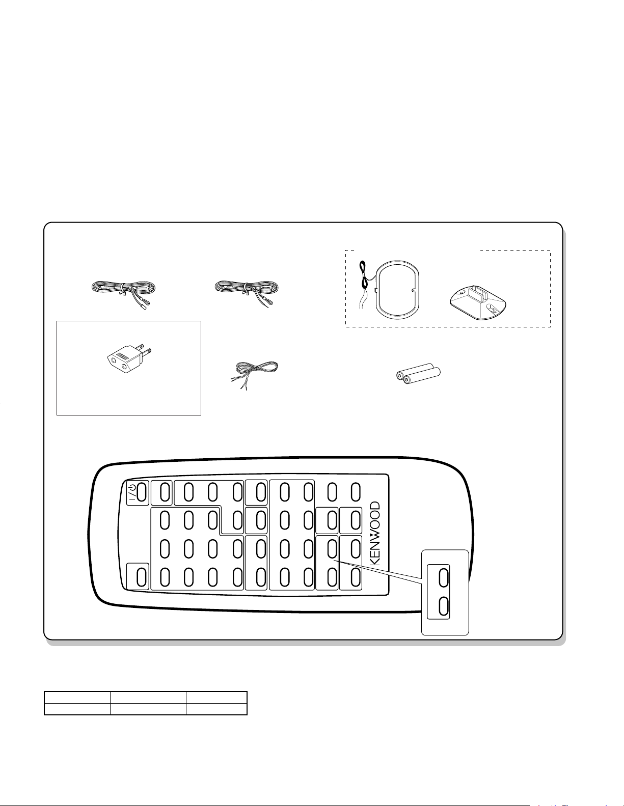
Batteries (R6/AA) (2)
Other countries
Remote
Battery cover (A09-0384-08)
control unit (1)
AM loop antenna stand (1)
Speaker cords (2)
Loop antenna (1) (T90-0833-05)
Please confirm that the following accessories are present.
FM indoor antenna (1)
Europe and U.K.
AC plug adapter (1)
Use to adapt the plug on the power
cord to the shape of the wall outlet.
(Accessory only for regions where
use is necessary.
1
32
N.B.
456
REPEAT
789
RANDOM
+10 0
PGM
CLEAR
O.T.E.
TAPE
O.T.E.
MD
AUX
MUTE
ENTER
DISC
SELECTOR
1
¡
4¢
2 3
7
%
fi
TITLE
SEARCH
TUNER
BAND
VOLUME
CONTROL
DOT
DISPLAY
TIME
DISPLAY
36
SLEEP
REMOTE CONTROL UNIT
RC-M1MD
TAPE MD C D
P.CALL
PTY
TA/
NEWS/INFO
REMOTE CONTROL UNIT
RC-981MD
(T90-0810-05): TE
(E03-0115-05)
(E30-5474-08)
(A70-1178-05) : RC-M1MD.......MH
(A70-1179-05) : RC-981MD.......TE
(T90-0801-05): MH
(J19-3645-05))
RXD-981MD
CONTENTS / ACCESSORIES
Contents
CONTENTS / ACCESSORIES ....................................2
EXTERNAL VIEW........................................................3
DISASSEMBLY FOR REPAIR.....................................4
CD MECHANISM DESCRIPTION ...............................5
CIRCUIT DESCRIPTION...........................................12
ADJUSTMENT.......................................................... 26
WIRING DIAGRAM....................................................29
Accessories
PC BOARD ................................................................30
SCHEMATIC DIAGRAM............................................39
EXPLODED VIEW .....................................................61
PARTS LIST...............................................................65
PARTS DESCRIPTIONS...........................................77
SPECIFICATIONS .......................................Back cover
System configuration
SYSTEM MAIN UNIT SPEAKER
XD-981MD RXD-981MD LS-N651
2
Page 3
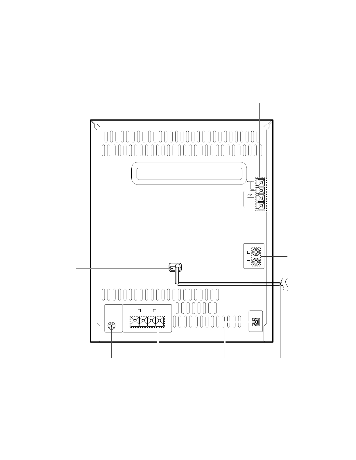
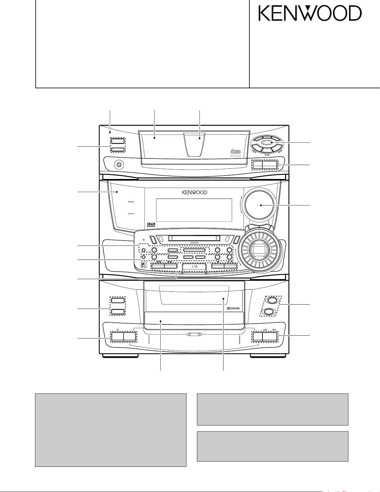
EXTERNAL VIEW
ANTENNA
AM FM
300Ω
FM
75Ω
GND
SUPER
WOOFER
PRE OUT
SPEAKERS
i6-16‰ j
RR LL
+
--
+
RR
LL
AUX INPUT
DIGITAL
INPUT
OPTICAL
RXD-981MD
Lock terminal board *
(E70-)
Power cord bushing
(J42-0083-05)
Phono jack
(E63-0164-05)
Lock terminal board
(E70-0057-05)
Optic receiving module
(W02-1181-05)
Phono jack
(E63-1024-05)
AC power cord *
(E30-)
* Refer to parts list on page 65.
3
Page 4
RXD-981MD
1
7
2
3
4
4
5
6
8
9
11
12
13
14
15
17
18
19
20
20
20
20
20
16
10
TOP
(Fig: a) (Fig: b)
TOP
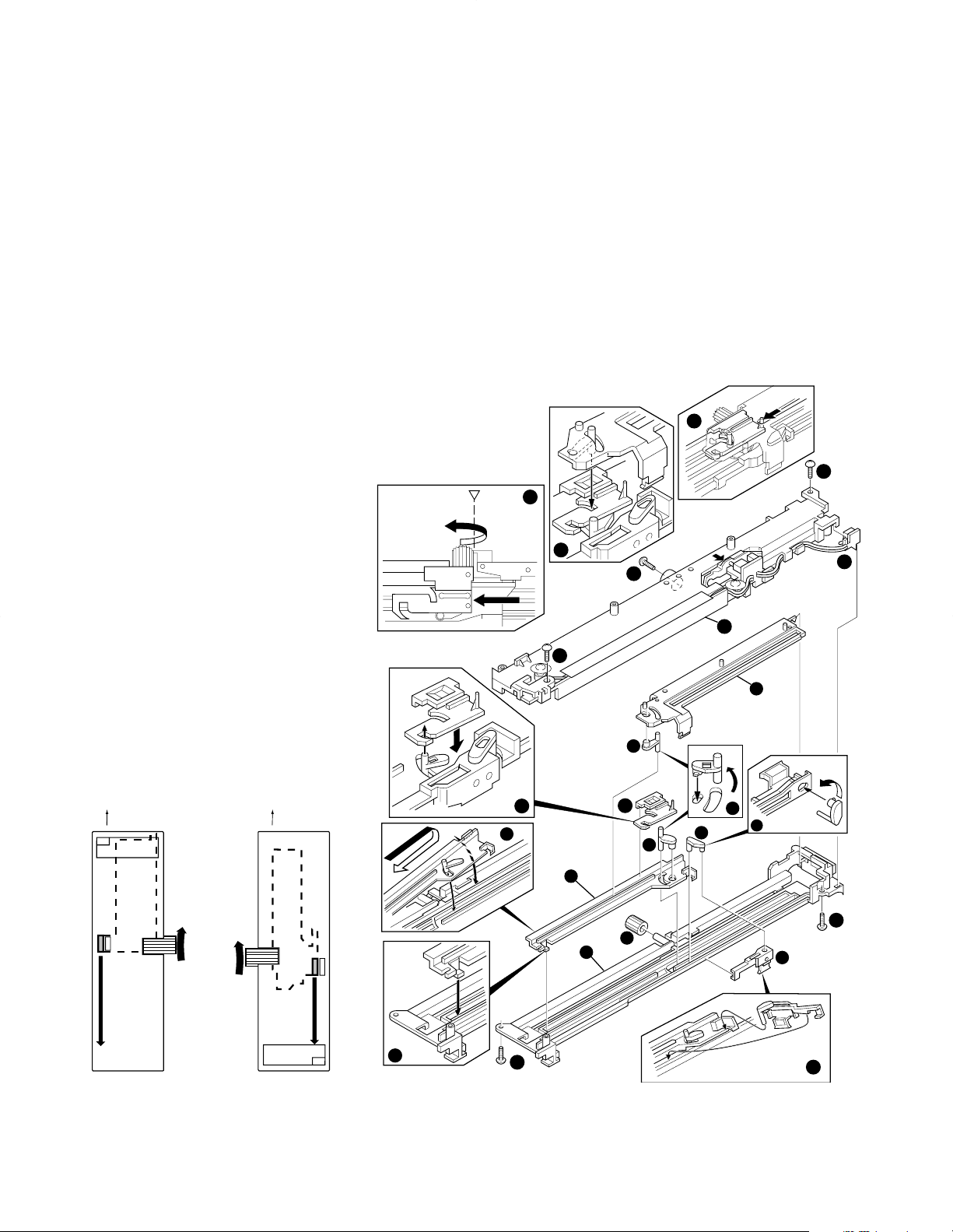
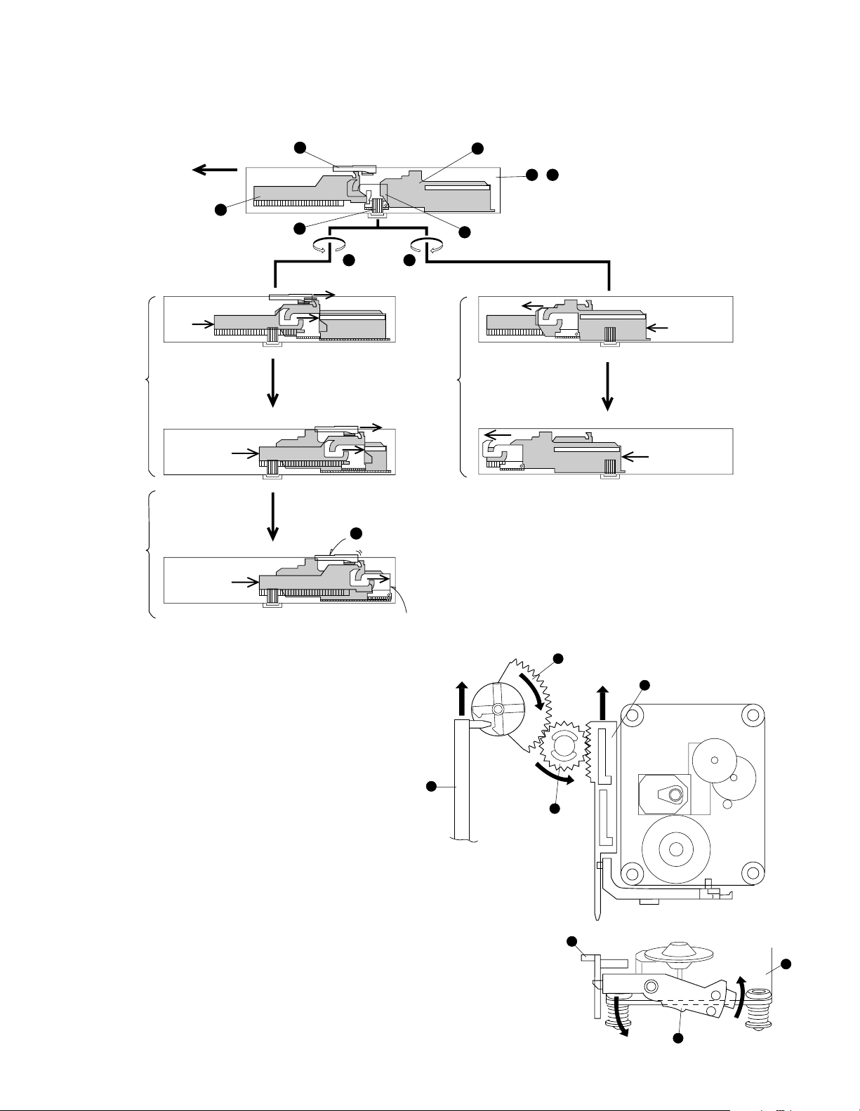
DISASSEMBLY FOR REPAIR
How to Assemble the Slider Ass'y in the
CD Mechanism
1. Mount the black lever1to the tray slider2 and assemble
them3.
2. Mount the white lever4 to the load slider5 and the open
slider6, and assemble them7.
3. Insert the gear9 to the groove of the holder8.
4. Insert the L shaped part of the load slider5 to the groove
of the holder8 and assemble them0.
5. Slide the load slider5 with lifting the edge of it rightwards.
Next insert the hook of the load slider5 and the boss of
the white lever4 to the groove of holder8. Then slide
the load slider5 to the fully leftward!.
6. Mount the tray slider 2 to the holder8 and assemble
them @.(note:Mount the tray slider2 to the wall of the
holder8)
7. Mount the slit of the center slider# to the boss of the
white lever4 and assemble them$.
How to Check the Slider Ass'y
After Assembly
Stand upright the slider ass'y before check
8. Slide the center slider# leftwards and position the right
edge of the gear9 to the right edge of center slider#.
Refer to %.
9. Position the boss of the open slider6 to the square hole
of the holder8 and slide the open slider6 fully rightwards. Mount the boss of the white lever4 assembled
with the open slider6 to the groove of the center
slider#.
Refer to ^.
10. Slide the center slider6 fully rightwards and slide the
boss of the center slider#.
Refer to &.
11. Mount the boss of the SW pcb to the slit of the holder8
and do holder* to the holder8. Then fix with screw).
Fig a: Turn the gear9 upwards and the tray
slider goes downwards smoothly. The
tray slider drops on the way.
Fig b: Turn the gear9 upwards and the open
slider goes downwards smoothly.
4
Page 5
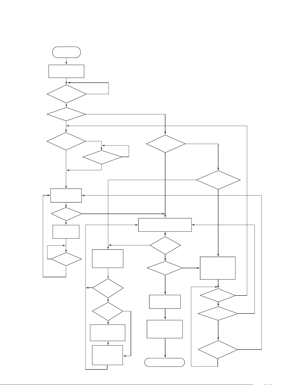
CD MECHANISM DESCRIPTION
START
Pickup moves
inwards
Pickup
position is at the
full inside?
No
No
No
No
No
No
No
No
No
No
No
No
No
No
No
Yes
Yes
Yes
Yes
Yes
Yes
Yes
Yes
Yes
Yes
Yes
Yes
Yes
Yes
Yes
Close ok
Open
position?
Top
position of
the holder?
Motor works
for close
Close ok?
Motor works
for open
Open ok?
Key pressed?
Motor works
for load and
load the holder
Top
position of
the holder
Clamp?
Meet with the
height of t.u
ass'y and
the holder
Motor works
for store and
return to
close position
Clamp with no disc
Clamp with no disc
Load or close
position?
Reset home position
of holder from bottom
In clamping?
Close
position?
t.u. ass'y
moves full
bottom
Reset home
position of holder
from bottom
Initial end
Slider position is poor
Clamp hoder
at top holder
position?
Motor works
for open and
set timer
to detect
"open error".
Open
position?
Close
position?
Motor start
time is over?
CD INITIALIZE FLOWCHART
RXD-981MD
5
Page 6
RXD-981MD
UP
DOWN
LIFT
1
2
3
a
b
b
c
b
a
c
b
CLOSE
OPEN
LOAD
UNLOAD(STORE)
a
b
c
OPEN WAIT
(RIGHT SIDE VIEW)
(TOP VIEW)
(FRONT VIEW)
CLAMP UNCLAMP
(RIGHT SIDE VIEW)
(SIDE VIEW of TU ass'y)
LOAD
Slider ASS'Y
PLAY
Hook of slider
TRAY
TRAY NO.
TRAVERSE UNIT ASS'Y
(T.U. ass'y)
CD MECHANISM DESCRIPTION
1. CD BANK MECHANISM
1-1 Function of Item Word
Function word is available in the figure.
1-2 Function of Parts
Tray... .........Each tray works in load mode only
Slider ass'y ... Lift mode(7 steps linked height). Hook of the slider ass'y in the load mode
T.U. ass'y.......Lift mode(3-steps linked the tray)
1-3 Clamp/Unclamp
6
Page 7
1
2
3
Hook of
OPEN @
TRAVELING
AREA of OPEN hook
TRAVELING
AREA of LOAD hook
Hook of
LOAD !
TRAY NO
(FRONT VIEW) (RIGHT SIDE VIEW)
FRONT REAR
LIFT MOTOR LOADING MOTOR
(TOP VIEW)
< PARTS LOCATION >
RXD-981MD
CD MECHANISM DESCRIPTION
1-4 Function of Lift and Load Mode
Ex: Disc-2 Playback from The Tray Open.
• Close the tray-2(loading)
• Lift the slider ass'y(lifting)--- To lift the T.U.
• Lift the T.U.ass'y(lifting)
• Move the slider ass'y downwards(lifting)----To meet the height of the slider ass'y with the tray-2.
• Load the tray-2.
• Clamp the CD disc on the tray-2(loading)
• Lift the holder ass'y up(lifting)----- To return in home position(HP)
• Move the slider ass'y from playback to waiting position.
• End.
1-5 Home Position(HP)
• Figure shows parts location at the home position.
• Each part in the home position
• Tray ---- Waiting
• Slider ass'y ----- Top
• Hook of sliders ------ Center
• T.U. ass'y ------ Bottom(Tray-3),unclamp
2. Motor Function
7
Page 8
RXD-981MD
21
b
b
a
a
< LOAD FUNCTION >
26
32
2
25
20
8
23
46
48
a
a
b
b
< LIFT FUNCTION >
Hook of OPEN
Hook of LOAD
TRAY 1
H.P. (no disc) (7th step)
< 7STEPS VS SLIDER ASS'Y >
1 LOAD/UNLOAD (6th step)
1 OPEN/CLOSE (5th step)
2 LOAD/UNLOAD (4th step)
3 LOAD/UNLOAD (2nd step)
2 OPEN/CLOSE (3rd step)
3 OPEN/CLOSE (1st step)
TRAY 2
TRAY 3
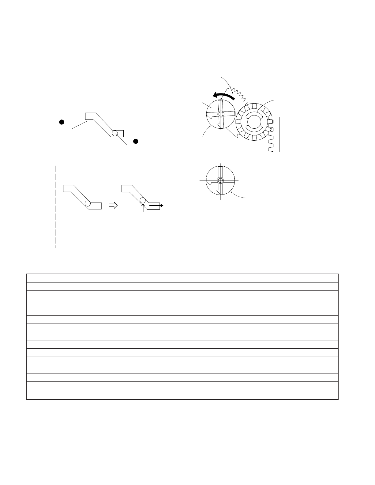
CD MECHANISM DESCRIPTION
• The lift motor turns counterclockwise a and the friction
arm¤ moves leftwards. The arm meet with the J shaped
rack gear of the lift-L slider. The slider moves backwards
The slider has 7 steps cam and it makes up or down
mode.
• The lift motor turns clockwise b and the slider2 moves
frontwards. The slider ass'y moves upwards.
• The gear§ separates from the J shaped rack gear and
gears into the gear∞. The gear∞ linked with the gear)
turn counterclockwise and T.U. ass'y move upwards.
• Namely up and down modes repeat.
• The friction arm¤ is the free position in the home position. T.U.ass'y moves upwards if the lift motor turns
counterclockwise.
8
Slider ass'y vs Height(7 steps)
2-1 Load Function
2-1-1 The slider of the slider ass'y backwards if the loading
motor turns counterclockwise(UNLOAD,OPEN MODE)
2-1-2 The slider of the slider ass'y frontwards if the loading
motor turns clockwise(LOAD,CLOSE MODE)
Page 9
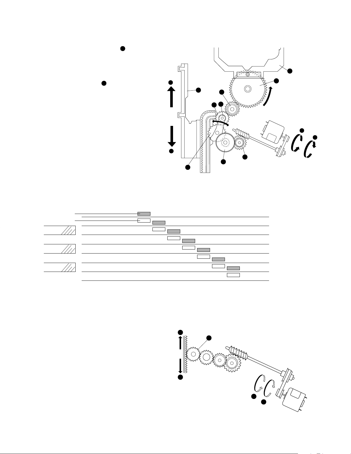
CD MECHANISM DESCRIPTION
15
4 5
33
36
21
a
b
14
36
OPEN
LOAD
CLAMP
,
Home
position
Slider (tray) ass'y
OPEN
Slider (open)
Slider (load)
Slider (center)
stops
continue to move
14
30
13
13
16
78
29
< CLAMP, UNCLAMP >
2-2 Each Slider Function in Slider Ass'y
RXD-981MD
The sliders(‹,$,fl) moves to LOAD if turn the gear¡
counterclockwise in the home position. The sliders separates and the sliders($ and ‹) moves more rightwards and the clamp mode starts after LOAD is over.
2-3 Clamp/Unclamp Function
The slider$ kicks the cross part of the gearº by load
mode. The gearª turns and moves the slider lack
gear# to LOAD by the door of the tray. Then the
slider# pushes the lever^ and T.U. ass'y moves
upwards. The clamp function starts by lifting the
T.U.ass'y.
The slider‹ moves to leftwards if the gear¡ turns clockwise in the home position. Then the open mode straits by
the sliders%,‹.
9
Page 10
full counter
clock wise
like time 8:27
TU Gear
(Ribs make a right angle)
Right angle is NG.
(out of 1 tooth)
zeneba gear
RXD-981MD
slider (CLAMP)
out of 1tooth
Boss of LEVER
(CLAMP)
< GOOD >
< NO GOOD >
13
16
CD MECHANISM DESCRIPTION
How to Assemble the Gear (zeneba)
The zeneba gearº has to meet the timing.
The T.U. ass'y doesn't work the clamp if the zeneba gear is
1 tooth out of the right position.
FUNCTION of SWITCH and MOTOR
Ref No. Parts Name Description
LM tray motor The motor for the slider(open,close load store)
LFTM lift motor The motor for the lift(holder up/down, T.U.height)
S1 open sw The switch for the position detector in the slider-open(Low active)
S2 close sw The switch for the position detector in the slider-close(Low active)
S3 load clamp sw The switch for the position detector in the slider-load(Low active)
S4 unclamp sw The switch for the position detector in the disc unclamp of the T.U.(Low active)
S5 tu height a sw The switch A for the height detector in the T.U.(Low active)
S6 tu height b sw The switch B for the height detector in the T.U.(Low active)
S7 home position sw The switch for the home position detector in the slider(Low active)
S8 count sw The switch for the height detector in the holder(Low active)
S9 center boss sw The switch for the disc position detector in the stocker(Low active)
PTR1 disc sensor The switch for the disc detector in the close mode(Low active)
SLT.SW start limit sw The switch for the most inner position detector of the pickup.
IC208(X09) LM speed control To control the speed of the tray motor.(L:speed down)
10
Page 11

RXD-981MD
CD MECHANISM DESCRIPTION
ACTUAL OPERATIONS (Refer page 8)
EX 1: Playback the Disc-1 in the All Discs Load
Load the disc-1 The slider ass'y moves
down by 2 steps (the 5th step)
ó
The tray-1 opens
ó ....................Load the disc
The tray-1 closes
ó
The slider ass'y moves
up by 2 steps (the H.P.)
ó
Load the disc-2 The slider ass'y moves
down by 4 steps(the 3rd step)
ó
The tray-2 opens
ó ....................Load the disc
The tray-2 closes
ó
The slider ass'y moves
up by 4 steps(the H.P.)
Load the disc-3 The slider ass'y moves
down by 6 steps(the 1st step)
ó
The tray-3 opens
ó ....................Load the disc
The tray-3 closes
ó
The slider ass'y moves
up by 6 steps (the H.P.)
ó
Playback the disc-1 The T.U. ass'y moves
up by 2 steps (tray-1 height)
ó
The slider ass'y moves
down by 1 step(the 6th step)
ó
Clamp the disc-1
ó
The slider ass'y moves
down by 1 step(the H.P.)
ó
Load the tray-1 of the no disc.
ó
Playback the disc
EX 2: Change to the Disc-3 in Playbacking
the Disc-1(There are discs on the tray1 and 2)
Unload the tray-1 Load the tray-1 of the no disc.
ó
The slider ass'y moves
down by 1 step(the 6th steps)
ó
Unclamp the tray-1
ó
The slider ass'y moves
up by 1 step(the H.P.)
ó
Playback the tray-3 The T.U. ass'y moves
down by 2 steps(tray-3 height)
ó
The slider ass'y moves
down by 5 steps(the 2nd steps)
ó
Load the tray-3 and
clamp the disc-3
ó
The slider ass'y moves
up by 5 steps(the H.P.)
ó
Load the tray-3 of the no disc.
ó
Playback the disc-3
EX 3: Change to the Disc-2 and Playback it in Playbacking the Disc-1
Open the tray-2 The slider ass'y moves
down by 4 steps(the 3rd steps)
ó
Open the tray-2
ó ....................Change the disc
Close the tray-2
ó
The slider ass'y moves
up by 4 steps(the H.P.)
Unload the tray-1 ó
Load the tray-1 of the no disc.
ó
The slider ass'y moves
down by 1 step(the 6th steps)
ó
Unclamp the tray-3
ó
The slider ass'y moves
up by 1 step(the H.P.)
Playback the tray-2 ó
Change the height
of the T.U. ass'y
(3î1î2/down-up*) ...*1skip the 2nd
step if down
ó mode.
The slider ass'y moves
down by 5 steps(the 2nd step)
ó
Clamp the disc-3
ó
The slider ass'y moves
down by 5 step(the H.P.)
ó
Load the tray-2 of the no disc.
ó
Playback the disc-2
11
Page 12
RXD-981MD
CIRCUIT DESCRIPTION
1. Initialization
1-1 Setting of initial conditions
While pressing the [ENTER] key, plug the AC power cord
into an AC power outlet.
1-2 Initializing operation
• A microcomputer is initialized for start when the AC
power is turned on while pressing the [ENTER] key. At
that time, CD mechanism, MD mechanism and CASSETTE mechanism are also initialized.
• During the initial operation, the display shows “INITIALIZE” and after that the clock blinks up on display.
1-3 Initial items and back up data
ITEMS
✣ POWER OFF
✣ VOLUME 15
✣ BALANCE CENTER
✣ MUTING OFF
✣ EQ OFF
✣ EQ. MANU FLAT
AMP ✣ EX. BASS ON
✣ SURROUND OFF
✣ INPUT SEL TUNER
✣ AUX INPUT 0 (-6dB)
✣ N. B. OFF
✣ DEMO OFF
✣ BAND FM
✣ LAST f LIMIT
TUNER ✣ LAST Pch ——
✣ AUTO/MONO AUTO
✣ Pch TEST f
✣ CLOCK AM 12 : 00
✣ PROG ON AM 12 : 00
CLOCK ✣ PROG OFF AM 12 : 00
TIMER ✣ PRO MODE PLAY
✣ SOURCE TUNER
✣ Pch 1
✣ EXE OFF
✣ OTT OFF
SLEEP OFF
PLAY MODE TRACK
REPEAT OFF
CD RANDOM OFF
PLAY MODE STOP
TIME SINGLE
✣ DIRECTION FORWARD
DECK ✣ RVS MODE p
✣ DOLBY NR OFF
OPERATION MODE STOP
✣ back up data
1-4 Mechanism initialization
1-4-1 CD mechanism
• If a mechanism error occurs, “C” is indicated on the
display.
1-4-2 MD mechanism
• The MD ON code is input within 4 seconds after turned
the power port on, the MD initial code (D122H) is output.
If the MD on code is not input, the error indication is
displayed as "M" on the display.
1-4-3 CASSETTE mechanism
• If a mechanism error occurs, "X" is indicated on the display.
1-5 All RAM clear
While pressing [SET] key, plug the AC power cord into
an AC power outlet, the all RAM cleared.
2. TUNER preset frequency
ch
1 FM 97.50MHz FM 97.50MHz
2 FM 108.00MHz FM 108.00MHz
3 AM 630kHz AM 630kHz
4 AM 1000kHz AM 999kHz
5 AM 1440kHz AM 1440kHz
6 AM 1610kHz AM 1602kHz
7 FM 87.50MHz FM 87.50MHz
8 FM 87.50MHz FM 87.50MHz
9 FM 87.50MHz FM 87.50MHz
10 FM 89.10MHz FM 89.10MHz
11 FM 87.50MHz FM 87.50MHz
12 FM 90.00MHz FM 90.00MHz
13 FM 106.00MHz FM 106.00MHz
14 AM 530kHz AM 531kHz
15 FM 87.50MHz FM 87.50MHz
16 FM 98.00MHz FM 98.00MHz
17 FM 98.50MHz FM 98.50MHz
18 FM 87.50MHz FM 87.50MHz
19 AM 990kHz AM 990kHz
20 FM 97.40MHz FM 97.40MHz
21 FM 87.50MHz FM 87.50MHz
22 FM 87.50MHz FM 87.50MHz
23 FM 87.50MHz FM 87.50MHz
24 FM 87.50MHz FM 87.50MHz
25 FM 87.50MHz FM 87.50MHz
26 FM 87.50MHz FM 87.50MHz
27 FM 87.50MHz FM 87.50MHz
28 FM 87.50MHz FM 87.50MHz
29 FM 87.50MHz FM 87.50MHz
30 FM 87.50MHz FM 87.50MHz
31 FM 87.50MHz FM 87.50MHz
32 FM 87.50MHz FM 87.50MHz
33 FM 87.50MHz FM 87.50MHz
34 FM 87.50MHz FM 87.50MHz
35 FM 87.50MHz FM 87.50MHz
36 FM 87.50MHz FM 87.50MHz
37 FM 87.50MHz FM 87.50MHz
38 FM 87.50MHz FM 87.50MHz
39 FM 87.50MHz FM 87.50MHz
40 FM 87.50MHz FM 87.50MHz
K2 E1/E2/H
Destination
12
Page 13
RXD-981MD
GC-E6003
X09, IC2
X14, IC1
X14, IC2
X09
IC61
X09
IC203
X09
IC402
X09
IC403
X14
IC3
E TYPE
ONLY
X09, IC7
CD mechanism
Mechanism
control
circuit
Mechanism
control
circuit
Auto reverse
cassette
mechanism
Head amp
dolby B
HA12209F
CXD2587Q
TUNER
PLL IC
LC72131
AUDIO
AMP SYSTEM IC
(LC75396)
MD
MDM-97A
LCD
LED
X14 ED1
FL
BJ573GK
Key matrix
encoder
remocon
RDS
demodulator
DOT driver
LC75710NE
E ONLY
BU2090
LED ariver
BU2090
M30612MA-306
FP
u-COM
CIRCUIT DESCRIPTION
3. Destination list of TUNER
Desti- U-COM Discrimination Receiving frequency Channel PORT
nation Desti- DSW1 DSW0 Band range space IF RF 92
– – K2 – – FM 87.5MHz~108.0MHz 100kHz +10.7MHz 25kHz 1
H, X H 1 0 FM 87.5MHz~108.0MHz 50kHz +10.7MHz 25kHz 0
Y, M, I E1 0 1 FM 87.5MHz~108.0MHz 50kHz +10.7MHz 25kHz 0
C, V AM 531kHz~1602kHz 9kHz +450kHz 9kHz 0
E, T E1 1 1 FM 87.5MHz~108.0MHz 50kHz +10.7MHz 25kHz 0
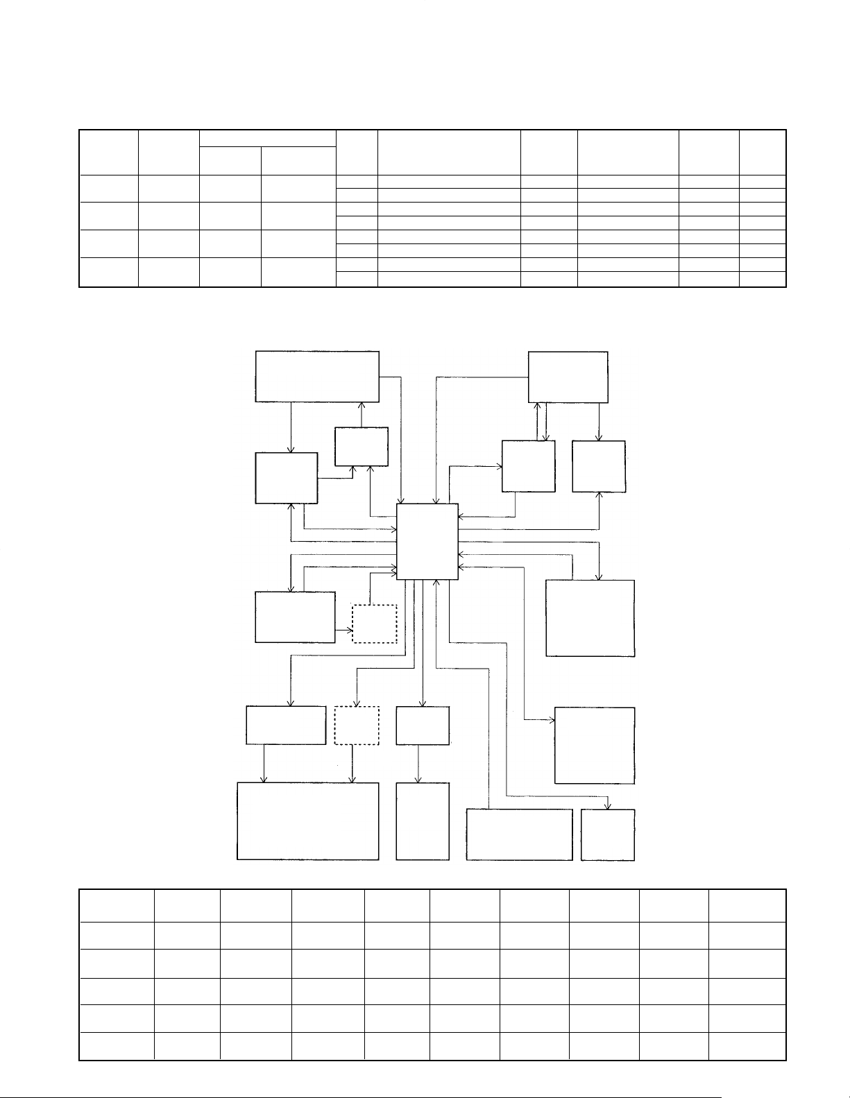
4. Composition
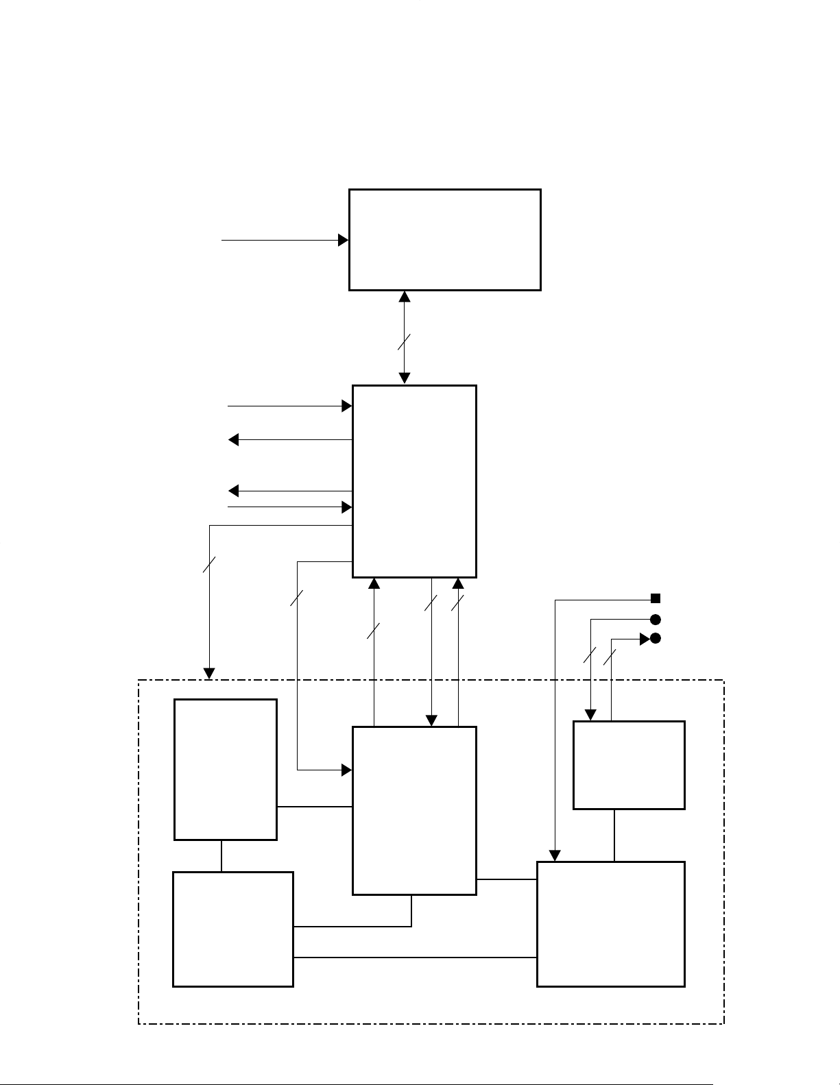
4-1 Microprocessor periphery block diagram
nation (65pin) (66pin)
AM 530kHz~1610kHz 10kHz +450kHz 10kHz 0
AM 531kHz~1602kHz 9kHz +450kHz 9kHz 0
RDS AM 531kHz~1602kHz 9kHz +450kHz 9kHz 0
0=(input low) 1=(input high)
4-2 Key matrix
REFERENCE VOLTAGE (5V)
Voltage 0.45 < 0.96 < 1.41< 1.85 < 2.29 < 2.74 < 3.20 < 3.64 < 4.10 <
<
0.96
KEY0 MODE EQ./ TAPE DOLBY TAPE TAPE TWIN TAPE KEY
94PIN BEATC. REC NR STOP PLAY REC O.T.E. OFF
KEY1 REW FF POWER MD MD MD QUICK T.EDIT/ KEY
93PIN 1¡ STOP 6 DELETE MOVE ADJ. OFF
=
KEY2 REPEAT SURRO- MD OTE TITLE TITLE MD SET ENTER KEY
<
=
1.41
<
1.85
=
<
=
2.29
<
=
2.74
<
=
3.20
<
=
3.64
<
4.10 210 <
=
92PIN /PROG. UND/OTT /EXE. INPUT SEARCH EJECT OFF
KEY3 DISPLAY RVS INPUT BEST REC MD EXBASS TUNER KEY
91PIN MODE SELECT HITS INPUT REC /A.P.S BAND OFF
KEY4 CD CD CD_3 CD_2 CD_1 CD_1 CD_2 CD_3 KEY
90PIN STOP 6 OPEN OPEN OPEN OFF
13
Page 14

RXD-981MD
CIRCUIT DESCRIPTION
4-3 Pin description of main microprocessor: M30612MA-306FP(X09: IC7)
Pin No. Name I/O Description
1 CE O PLL/system IC(chip enable)
2 PLL-DO I PLL(LC 72131)data input
3 SD I Tuner SD detector input H: NO tuned L: tuned
4 STEREO I Stereo(tuner) detector input H: MONO L: STEREO
5 EMPHASIS O Emphasis change-over(M type only) H: 100K L: 50K
6 RDS-DATA I RDS data signal input(E type only)
7 CE I Power failure input H: AC ON L: AC OFF
8,9 BYTE,CNVSS I No used
10 XCIN I
11 XCOUT O
12 RESET I Reset H: Normal L: Reset
13 XOUT O Main clock output(10MHz)
14 VSS – GND
15 XIN I Main clock input(10MHz)
16 VCC – u-com power supply
17 NMI I +5V(VCC terminal)
18 REMOCON I Remote control input
19 RDS-CLK I RDS IC clock
20 SCOR I Sub code synchronism signal(CXD2587Q)
21 CD SW3 I CD mecha. SW3 H: OFF L: ON
22 LCD DATA/CLOCK O LCD DATA/CLOCK
23 CD SW1 I CD mecha. SW1 H: OFF L: ON
24 CD SW2 I CD mecha. SW H: OFF L: ON
25~27 CD SW5~CD SW7 I CD mecha. SW5~7 H: OFF L: ON
28 SQCK O Sub code clock(CXD2587Q)
29 SUBQ I Sub code data
30 N.C. – No used
31 FL DATA O FL driver data output(LC75710NE)
32 SW8 I CD mecha. SW8 H: OFF L: ON
33 FL CLK O Clock output for FL driver(LC75710NE)
34 FL CE O Chip enable output for FL driver(LC75710NE)
35 MD TX O TX data output to MD
36 MD RX I RX data input from MD
37 FL RST O Reset output for FL driver(LC75710NE) H: normal L: reset
38 LDC O CD laser control output H: OFF L: ON
39 CD MUTE I CD zero mute input H: OFF L: ON
40 SLCK O CD sense data read clock(CXD2587Q)
41 SENSE I CD sense input(CXD2587Q)
42 CD-CLK O CD DSP clock(CXD2587Q)
43 XLAT O CD latch output(CXD2587Q)
44 CD-DATA O CD DSP data(CXD2587Q)
45 XRST O CD DSP reset output(CXD2587Q) H: normal L: reset
46 DC OFF O CD DSP power supply H: ON L: OFF
47 DREC SEL O MD digital input selector H: digital in L: others
48 SENSOR I CD mecha. sensor H: OFF L: ON
49 M UP O CD mecha. up H: ON L: OFF
50 M OPEN O CD mecha. open H: ON L: OFF
51 TMC O CD mecha. speed control H: slow L: fast
52 M CLOSE O CD mecha. close H: ON L: OFF
53 M DOWN O CD mecha. down H: ON L: OFF
54 CD SW4 I CD mecha. SW4 input(unclamp) H: OFF L: ON
55 CD BOS I CD mecha. bos sensor input H: OFF L: ON
56 ENC4 I Rotary encoder4/Vol. input A
57 ENC3 I Rotary encoder3/Vol. input B
58 ENC2 I Rotary encoder2/Jog input A
59 ENC1 I Rotary encoder1/Jog input B
60 LED CLK O Clock output for LED driver
Timer clock input/output(32.768kHz)
14
Page 15
RXD-981MD
CIRCUIT DESCRIPTION
Pin No. Name I/O Description
61 RES/FL DATA O Reset for FL driver
62 VCC – +5V(VCC terminal)
63 LED DATA O LED driver DATA output (BU2090)
64 VSS – GND
65,66 DSW1, DSW0 I Model discrimination
67 CD SW11 I CD mecha. load on sensor input H: OFF L: ON
68 REC/PLAY O Deck REC/PLAY change-over H: REC L: PLAY
69 BEAT C O Deck beat cancel H: ON L: OFF
70 SOL O Deck solenoid control H: ON L: OFF
71 CPM O Deck motor control H: ON L: OFF
72 REC MUTE O Deck rec mute control H: OFF L: ON
73 BIAS O Deck bias control H: ON L: OFF
74 DOLBY O Deck dolby control H: ON L: OFF
75 DPSS I Deck DPSS detection input L: ON music signal
76 REC R SW I Reverse rec detection SW L: inhibited
77 REC F SW I Forward rec detection SW L: inhibited
78 PACK SW I Deck pack SW input H: OFF L: ON
79 PLAY SW I Deck play SW input H: OFF L: ON
80 CLK O Clock output to LC75396/LC72131
81 A-MUTE O Mute control H: ON L: OFF
82 VOL ATT O Vol attenuation H: ON L: OFF
83 POWER O Power control H: ON L: OFF
84 PROTECT I Protection input H: Protect L: Normal
85 SP RELAY O Speaker relay control
86~88 SSELA~SSELC O Speana band selection(A,B,C)
89 BP IN I Speana input
90~94 KEY4~KEY0 O A/D input for keys(KEY4~KEY0)
95 RDS S LEVEL I RDS signal level
96 AVSS – A/D GND
97 PHOTO O Reel pulse input
98 VREF – A/D reference voltage
99 AVCC – +5V(VCC terminal)
100 DATA O Data for LC75396E/LC72131
4-4 Pin description of expander IC: BU2090 (X14, IC2)
Pin No. Name I/O Description
1 VSS – GND
2 DATA I DATA INPUT TERMINAL
3 CLOCK I CLOCK TERMINAL
4 TAPE_REC O TAPE REC LED H=OFF L=ON
5 TAPE_RVS O TAPE RVS LED H=OFF L=ON
6 TAPE_FWD O TAPE FWD LED H=OFF L=ON
7~9 DISC3~1 O CD DISC3~1 LED H=OFF L=ON
10 EQ O EQ LED H=OFF L=ON
11 TAPE_DOLBY O TAPE DOLBY LED H=OFF L=ON
12 MD_REC O MD REC LED H=OFF L=ON
13 POWER O STANDBY LED H=OFF L=ON
14 SURROUND O SURROUND LED H=OFF L=ON
15 MD_SLOT O MD SLOT LED H=OFF L=ON
16 VDD – POWER SUPPLY
15
Page 16
RXD-981MD
Back up power
supply (+5V)
X09, IC7
X09, IC8
MAIN u-COM
M30612MA-306FP
ENG_KANA
MD_MUTE
MUTE AND OR
(MAIN u-COM)
back up sw
MD SUPPLY VOLTAGE
CHANGE-OVER
TERMINAL
MD_RESET
MD-ST
SEARCH
LOAD_IN
DSCK
K_DATA
DSTB
MD_DATA
uart
rxd
txd
digital in
analog L/R in
analog L/R out
AD / DA
CONVERTER
MD
CONTROL
u-COM
DRIVE
UNIT
MD u-DOM
RF AMP
ENDEC / ATRAC
MD mecha. unit (MDM-97A)
2
22
2
2
1
3
1
uPD78058GC-A59
• DISPLAY CONTROL
• RF AMP CONTROL
• SIGNAL PROCESSING IC
CONTROL (TUNER)
• VOLUME, MUTE CONTROL
• INPUT SELECTOR CONTROL
back up voltage detection
5. Composition (MD section)
5-1 Microprocessor periphery block diagram
CIRCUIT DESCRIPTION
16
Page 17

RXD-981MD
CIRCUIT DESCRIPTION
5-2 Pin description of MD u-COM: uPD78058GC-A59
Pin No Name I/O Description
1 PDOWN O MDM-97 POWER DOWN DETECTOR
2 SEARCH O CD SEARCH OUTPUT
3 LOAD IN I LOAD SWITCH INPUT
4 Avss – A/D POWER SUPPLY (CONNECTED TO GND)
5,6 – – NO USED
7 Avref1 – D/A REFERENCE VOLTAGE(+5V)
8 RXD I COMMUNICATION FROM MAIN u-COM (UART RXD)
9 TXD O COMMUNICATION TO MAIN u-COM (UART TXD)
10 – – NO USED
11 MD_DATA I MD IC IN DATA (MDM-97 IN DATA)
12 K_DATA O MD IC OUT DATA (MDM-97 OUT DATA)
13 DSCK O MD IC CK (MDM-97 CLOCK)
14 DSTB I MD IC STB (MDM-97 STB)
15 COMM_ANS I NO USED
16 COMM_DIN I NO USED
17 COMM_DOUT O NO USED
18 COMM_CLK I/O NO USED
19 COMM_REQ O NO USED
20~31 – – NO USED
32 MD VLOAD O MD LOAD VOLTAGE CHANGE-OVER DISC LOAD/EJECT : H OTHER : L
33 Vss – u-COM(CONNECTED TO GND)
34~43 – – NO USED
44 INISW I INITIAL SW (H : RXD-981MD L : J TYPE)
45~58 – – NO USED
59 SRESET O NO USED
60 RESET I u-COM RESET
61 REMOCON I REMOCON INPUT (NO USED)
62~66 – – NO USED
67 CE I u-COM CE
68 Vdd – u-COM POWER SUPPLY
69 X2 – 5MHz OSCILLATOR
70 X1 I 5MHz OSCILLATOR
71 IC – IC TERMINAL(CONNECTED TO GND)
72 XT2 – NO USED (OPEN)
73 XT1 I NO USED (CONNECTED TO GND)
74 Avdd – A/D POWER SUPPLY
75 Avref0 I A/D REFERENCE VOLTAGE
76 BACKUP I
77 AMUTE O ANALOG MUTE H : MUTE ON L : MUTE OFF
78 BACKUPSW O BACKUP DETECTOR SW H:ON(IN CASE of CE : HIGH) L:OFF(IN CASE of CE LOW)
79 MD_RESET O MD u-COM RESET H : NORMAL L : MD u-COM RESET (LOW EDGE)
80 MD_ST O MD ON/CD SYNC H : MD ON L : BACKUP MODE
BACKUP DETECTOR(A/D)
BACK UP : MORE THAN2.2V NO BACKUP:LESS THAN2.2V
6. Test mode
6-1 Test mode of the receiver
(1) Setting of the test mode
While pressing the [INPUT] key or [Band] key, plug the
AC power cord into an AC power outlet.
(2) Canceling of the test mode
Unplug an AC power cord.
(3) Condition in test mode
POWER • • • • • • ON
SELECTOR • • • AUX (in case of [INPUT] key)
TUNER (in case of [BAND] key)
FL, LED • • • • • • All the fluorescent display indicate and
LEDs light. (The all illuminated state is
cleared by pressing any main unit key
or remocon key.
EX. BASS • • • • • OFF
(4) Basic operation in test mode.
1 The muting during mode selection is not controlled in
the test mode.
2 The test mode is cancelled when the AC power is
turned OFF.
3 The operation of the keys in the test mode, as follows.
(5) The operation of the keys in the test mode.
1 DISP key
When this key is pressed in the test mode, all the fluorescent light off and normal display are indicated
cyclically. (FL, LED, LCD)
17
Page 18
RXD-981MD
KEY
INDICATION
OF VOL.
VALUE
Press mode key in the AUX mode
1 time
2 times
BALANCE
INPUT LEVEL
TRACK EDIT1L
-6
DELETE
44 (MID)
CENTER
0
QUICK MOVE
86 (MAX)R+3
CIRCUIT DESCRIPTION
2 REPEAT key
If this key is pressed when setting the test mode, the
RDS indication is available on the display with the
selector on TUNER.
3 DISC 1~3 keys
With the selector on AUX, when the DISC 1~3 keys
are operated, the surround level settings can be
made as follows.
1 DISC 1 • • • • SURROUND level -10 (Min)
2 DISC 2 • • • • SURROUND level 0 (Center)
3 DISC 3 • • • • SURROUND level +10 (Max)
4 REC INPUT key
With the selector on TUNER, the fluorescent changes
cyclically as follows by pressing the REC INPUT key.
• ATT is switched OFF. “ATT OFF XX”
• ATT is switched ON. “ATT ON XX”
• ATT is switched OFF. Normal display
XX means A/D value (HEX) of S.
5 CD STOP key
With the selector on TUNER, when the [CD STOP]
key operated, the preset memory can be changed as
10 steps.
î10
– –
î 20
– –
î 30
– –
î 40
– –
î 01 ì
6 TITLE INPUT/TITLE SEARCH/TWIN REC keys
With the selector on something other than TUNER,
the E.Q (Flat, Min, Max) settings can be made by
pressing the TITLE INPUT/TITLE SEARCH/TWIN
REC keys.
TWIN REC key E.Q Flat
TITLE INPUT key E.Q Min
TITLE SEARCH key E.Q Max
7 JOG DIAL key
With the selector on TUNER, the P. CALL is operated
by turning the JOG DIAL key.
JOG DIAL(CW) P.CALL up
JOG DIAL(CCW) P. CALL down
8 CD DISC1 OPEN/CLOSE key
With the selector on TUNER, the channel space settings can be made cyclically by pressing the DISC
OPEN/CLOSE key with E1 version.
9 Other keys
During the test mode, it can be operated in a special
manner that is different from an ordinary operation by
using the keys on the main body, specifically as
shown in the following table.
6-2 Test mode of DECK section
(1) Setting
While pressing the PLAY key(DECK), plug the AC
power cord into an AC power outlet.
(2) Resetting
• Disconnect the AC power cord from an AC power outlet or press the [ON/STANDBY] key.
(3) Operation in TEST mode
(a) Initial condition
Item Condition
Power ON
Selector TAPE
Main VOL. -63dB(VOL.17)
Input level(AUX) -6dB(Input0)
EX. bass OFF
FL, LED, LCD All the FLs, LEDs,
and LCDs are turned on
(b) 4-sec REC
If the REC key is pushed, the system record for 4sec.
Then, it rewinds to the REC starting position and
plays back automatically.
If the REC key is pushed during the 4-sec REC operation, the system records further for 4-sec, then
returns to the starting position of the first 4-sec REC
operation and plays back.
(c) Mechanism SW detection
SW Display
FWD REC Inhibit SW Calendar-1
RVS REC Inhibit SW Calendar-2
(d) O.T.E / TWIN REC indication
The LCD changes cyclically as follows.
Keys Indication of LCD
O.T.E. î TAPE, O.T.E. (light ON) î
TAPE, O.T.E. (light OFF) í
TWIN REC î TWIN REC, O.T.E. (light ON) î
TWIN REC, O.T.E. (light OFF) í
(e) AUX input level
The AUX input level settings can be made as follows
by pressing keys.
Keys Input level
TRACK EDIT Min (-6)
DELETE Initial value (0)
QUICK MOVE Max (+3)
(f) REC PAUSE
When the REV. MODE key is pressed, the REC
PAUSE is entered during the REC operation.
18
Page 19
RXD-981MD
SEL.
MD
(PAUSE)
CD
DIGITAL
SP
SEL.
MD
(PAUSE)
AUX IN
(ANALOG)
REC IN
SP
1. Preparation for adjustment Test disc
6-3-2 MD TEST mode for adjustment
Type Test disc
1 High reflection disc TGYS1 (SONY)
2 Low reflection disc Recording minidisc
3 Head Adjusting transparent
2. Test mode Test mode setting method
1. While pressing the [TRACK EDIT] key, plug the AC power cord into an AC power outlet.
(State A is changed to state B .)
2. Insert the playback disc 1 (high reflection disc) or recording disc 2 (low reflection disc). (State C is set.)
Thus, the test mode state is set.
A MD
represents version of MD microcomputer.
(When the MD (STOP) button is pressed in the C state,
is restored. To restore C again,
press
the
B EJECT
TEST
C AUTO
TEST
Entering the specific mode
Whenever the [MD REC] button is pressed, the mode is changed.
AUTO pre-adjustment AUTO adjustment RESULT SUB RESULT
EEPROM setting MANUAL adjustment MANUAL pre-adjustment
(AUTO YOBI) (AUTO AJST) (RST YOBI) (RESULT)
(EEPROM SET) (MNU AJST) (MNU YOBI)
the indication D
[MD REC] button.)
D tsm
e : TEST MODE
TEST STOP state
• Canceling the test mode
When the POWER button is pressed, the test mode is canceled, and the POWER OFF state is set.
CIRCUIT DESCRIPTION
6-3 Test mode of MD player
6-3-1 Inspection mode
Setting : While pressing the [QUICK MOVE] Key, plug the AC power cord into an AC power outlet.
The "INSPECTION" shows on the display.
Cancellation : Unplug the AC power cord from an AC power outlet.
No.
1 Digital through TITLE INPUT
2 Analog through TITLE
Contents of
TEST mode
test mode
test mode SEARCH
Keys Operation & Indication RemarKs
• The "DIGITAL1" is indicated on the display for a
second. "DIGITAL1"îCD input
• The "DIGITAL 2" is indicated on the display for
a second. "DIGITAL 2"îExternal digital input
• The "DIGITAL1" and "DIGITAL 2" can be
changed cyclically by pressing the [TITLE
INPUT] Key.
• Source indicator (MD) is blinked.
• The "ANALOG" is indicated on the display for a
second.
• AUX input levelîMID
• Source indicator (AUX) is turned ON .
19
Page 20
RXD-981MD
2. AUTO adjustment mode
Step No.
Setting Method
Remarks Display
Step 1 Testmode STOP state [ t s m e ]
Step 2
Press the
MD REC button two times.
AUTO adjustment menu [ A U T O _ A J S T _ ]
Step 3 Press once the MD PLAY button. The slide moves to the innermost periphery, and automatic [ : _ _ _ _ _ _ ]
adjustment is started.
• In case of high reflection disc changes as follows.
PEG→HAG
•In case of low reflection disc changes as follows.
PEG→LAG→GCG→GEG→LAG
End of adjustment If adjustment is OK, Step 4.
If adjustment is NG, Step 7.
Step 4 Adjustment value output [ _ C O M P L E T E _ ]
Press the MD PLAY button. STEP 5
Press the MD STOP button. STEP 2
1. AUTO pre-adjustment mode (Low reflection disc only)
Step No.
Setting Method
Remarks Display
Step 1 Testmode STOP state [ t s m e ]
Step 2 Press once the MD REC button. AUTO pre-adjustment menu [ A U T O ]
Step 3 Press once the MD PLAY button. The slide moves to the innermost periphery, and automatic [ : _ _ _ _ _ _ ]
pre-adjustment is started.
• During automatic adjustment changes as follows.
HAo→RFg→SAg→SBg→PTG→PCH→GTG→GCH→RCG→
SEG→RFG→SAG→HAO→HEO→TCO→LAO
End of adjustment If adjustment is OK, Step 4.
If adjustment is NG, Step 5.
Step 4 Grating adjustment, [ _ C O M P L E T E _ ]
adjustment value output
Press once the MD STOP button. STEP 2
Step 5 Adjustment value output [ A U T Y O B I ]
Press once the MD STOP button. STEP 2 AUTO pre-adjustment menu
• : Adjustment name, : Address
• Test Mode
1. AUTO pre-adjustment mode • Automatic pre-adjustment is performed. (After adjustment the grating adjustment mode is set.)
• The adjustment value is output with the aid of system controller interface.
2. AUTO adjustment mode • Automatic adjustment is performed.
• The adjustment value is output with the aid of system controller interface.
• Continuous playback is performed. (Error rate indication, jump test)
3. RESULT sub-mode • The measurement value, set value and calculated value are indicated.
• The set value is changed manually (in servo OFF state).
4. RESULT mode (final adjustment) • The set value (after calculation) is indicated.
• The set value is changed manually (in servo OFF state).
5. MANUAL pre-adjustment mode • RF side manual adjustment is performed.
• Focus and tracking signal ATT manual adjustment is performed.
• Focus and tracking signal offset setting is performed.
6. MANUAL adjustment mode • Focus and tracking signal ATT manual adjustment is performed.
7. EEPROM setting mode
8. TEST-PLAY mode • Continuous playback from the specified address is performed.
• • C1 error rate measurement,
This mode is not used for service.
•
This mode is not used for service.
•
This mode is not used for service.
9. TEST-REC mode • Continuous recording from the specified address is performed.
• Change of record laser output (servo gain is also changed according to laser output)
10. EJECT mode • TEMP setting (of EEPROM setting)
CIRCUIT DESCRIPTION
20
Page 21

RXD-981MD
Step 11 Press once the
MD REC
button. Indication of measurement value [ S E G : _ _ _ ]
Step 12 Press once the
MD REC
button. Indication of measurement value [ S F G : _ _ _ ]
Step 13 Press once the
MD REC
button. Indication of measurement value [ H A O : _ _ _]
Step 14 Press once the
MD REC
button. Indication of measurement value [ H B O : _ _ _]
Step 15 Press once the
MD REC
button. Indication of measurement value [ H E O : _ _ _]
Step 16 Press once the
MD REC
button. Indication of measurement value [ H F O : _ _ _]
Step 17 Press once the
MD REC
button. Indication of measurement value [ L A O : _ _ _]
Step 18 Press once the
MD REC
button. Indication of measurement value [ L B O : _ _ _]
Step 19 Press once the
MD REC
button. Indication of measurement value [ L E O : _ _ _]
Step 20 Press once the
MD REC
button. Indication of measurement value [ L F O : _ _ _]
Step 21 Press once the
MD REC
button. Indication of measurement value [ T C O : _ _ _ _]
Step 22 Press once the
MD REC
button. Indication of adjustment error sequence No. [ Y O B : _ _ _ _]
Step 23 Press once the
MD REC
button. Indication of adjustment status [ D I F : _ _ _ _]
Step 24 Press once the
MD REC
button. Indication of pre-adjustment not completed (00)/completed (4B) [ A D J : _ _ _ _]
Step 25 Press once the MD STOP button. RESULT sub-menu state [ _ R S T _ Y O B I _ ]
• : Measurement value, : Adjustment value, : Other various informations
• Pressing the REC button causes reversing.
• When the FF (⁄) key is pressed while the setting is displayed, the setting increases, and a new setting is stored in RAM.
• When the FB (!) key is pressed while the setting is displayed, the setting increases, and a new setting is stored in RAM.
Step 1 Testmode STOP state [ t s m e ]
Step 2
Press the MD REC button four times.
RESULT menu [ _ R S T U L T _ _ _ ]
Step 3 Press once the MD PLAY button. Indication of set value [ H A G : _ _ _ ]
Step 4 Press once the
MD REC
button. Indication of set value [ H B G : _ _ _ ]
Step 5 Press once the
MD REC
button. Indication of set value [ L A G : _ _ _ ]
Step 6 Press once the
MD REC
button. Indication of set value [ L B G : _ _ _ ]
Step 7 Press once the
MD REC
button. Indication of set value [ P E G : _ _ _ ]
Step 8 Press once the
MD REC
button. Indication of set value [ P F G : _ _ _ ]
Step 9 Press once the
MD REC
button. Indication of set value [ G E G : _ _ _ ]
Step 10 Press once the
MD REC
button. Indication of set value [ G F G : _ _ _ ]
Step 11 Press once the
MD REC
button. Indication of set value [ G C G : _ _ _ _ ]
Step 12 Press once the MD STOP button. RESULT menu state [ _ R E S U L T _ _ _ ]
4. RESULT mode (final adjustment)
Step No.
Setting Method
Remarks Display
Step 5
Continuous playback (groove section)
[ a c ]
Step 6 Press the MD STOP button. STEP 2 AUTO adjustment menu
Step 7 Adjustment value output [ C a n ' t _ A D J . ]
Press the MD STOP button. STEP 2 AUTO adjustment menu
• : Adjustment name, : Measurement value, : Address
Step 1 Testmode STOP state [ t s m e ]
Step 2
Press the MD REC button three times.
RESULT sub-menu [ _ R S T _ Y O B I _ ]
Step 3 Press once the MD PLAY button. Indication of measurement value [ R F G : _ _ _ ]
Step 4 Press once the
MD REC
button. Indication of measurement value [ R C G : _ _ _ ]
Step 5 Press once the
MD REC
button. Indication of measurement value [ R T G : _ _ _ _ _ ]
Step 6 Press once the
MD REC
button. Indication of measurement value [ G T G : _ _ _ _ _ ]
Step 7 Press once the
MD REC
button. Indication of measurement value [ P C H : _ _ _ _ ]
Step 8 Press once the
MD REC
button. Indication of measurement value [ G C H : _ _ _ _ ]
Step 9 Press once the
MD REC
button. Indication of measurement value [ S A G : _ _ _ ]
Step 10 Press once the
MD REC
button. Indication of measurement value [ S B G : _ _ _ ]
3. RESULT sub-mode
Step No.
Setting Method
Remarks Display
Step No.
Setting Method
Remarks Display
CIRCUIT DESCRIPTION
21
Page 22

Step 11 Press once the
MD REC
button. Focus ATT (B signal) tentative setting [ S B g : ]
Step 12 Press once the
MD REC
button. RF side pit section TG adjustment [ P T G : _ _ ]
Step 13 Press once the
MD REC
button. Pit section COUT level setting [ P C H : _ ]
Step 14 Press once the
MD REC
button. Outer periphery move → RF side groove TG adjustment [ G T G : _ _ ]
Step 15 Press once the
MD REC
button. Groove section COUT level setting [ G C H : _ ]
Step 16 Press once the
MD REC
button. RF side TCRS adjustment [ R C G : _ _ ]
Step 17 Press once the
MD REC
button. Tracking ATT (A signal) setting [ S E G : ]
Step 18 Press once the
MD REC
button. Tracking ATT (B signal) setting [ S F G : ]
Step 19 Press once the
MD REC
button. Indication of tracking EFMIO measurement [ g M I : _ _ _ ]
Step 20 Press once the
MD REC
button. RF side pit section FG adjustment [R F G : _ _ ]
Step 21 Press once the
MD REC
button. Focus ATT (A signal) setting [ S A G : ]
Step 22 Press once the
MD REC
button. Focus ATT (B signal) setting [ S B G : ]
Step 23 Press once the
MD REC
button. Offset "0" setting → A signal offset measurement [ H A O : _ _ _ ]
Step 24 Press once the
MD REC
button. B signal offset measurement [ H B O : _ _ _ ]
Step 25 Press once the
MD REC
button. E signal offset measurement [ H E O : _ _ _ ]
Step 26 Press once the
MD REC
button. F signal offset measurement [ H F O : _ _ _ ]
Step 27 Press once the
MD REC
button. TCRS signal offset measurement [ T C O : _ _ _ ]
Step 28 Press once the
MD REC
button. A signal offset measurement [ L A O : _ _ _ ]
Step 29 Press once the
MD REC
button. B signal offset measurement [ L B O : _ _ _ ]
Step 30 Press once the
MD REC
button. E signal offset measurement [ L E O : _ _ _ ]
Step 31 Press once the
MD REC
button. F signal offset measurement [ L F O : _ _ _ ]
• : Measurement value, : Set value, : Account value
• If the FF (⁄) or FB (!) key is pressed is pressed during setting indication, the setting increases/decreases, and the new setting is stored
in RAM.
If the measurement value is within the OK range, "
" appears on the 8th character.
Step 1 Testmode STOP state [ t s m e ]
Step 2
Press the MD REC button six times.
MANUAL adjustment menu [ _ M N U _ A J S T _ ]
Step 3 Press once the MD PLAY button. Initial setting → Temperature measuring mode [ T M P : _ _ _ _ ]
Step 4 Press once the MD REC button. Laser ON [ L O N : _ _ _ _ _ _ ]
Step 5 Press once the MD REC button. Innermost periphery move → Tracking ATT (E signal) setting [ P E G : ]
Step 6 Press once the MD REC button. Tracking ATT (F signal) setting [ P F G : ]
6. MANUAL adjustment mode High reflection disc
Step No.
Setting Method
Remarks Display
•
: Measurement value
• Pressing the REC button causes reversing.
• When the FF(⁄) key is pressed while the setting is displayed, the setting increases, and a new setting is stored in RAM.
• When the FB(!) key is pressed while the setting is displayed, the setting increases, and a new setting is stored in RAM.
Step 1 Testmode STOP state [ t s m e ]
Step 2
Press the
MD REC button five times.
MANUAL auxiliary adjustment mode [ _ M N U _ Y O B I _ ]
Step 3 Press once the MD PLAY button. Initial setting → Temperature measuring mode [ T M P : _ _ _ _ ]
Step 4 Press once the
MD REC
button. Offset "0" setting → A signal offset tentative measurement [ H A o : _ _ _ ]
Step 5 Press once the
MD REC
button. B signal offset tentative measurement [ H B o : _ _ _ ]
Step 6 Press once the
MD REC
button. E signal offset tentative measurement [ H E o : _ _ _ ]
Step 7 Press once the
MD REC
button. F signal offset tentative measurement [ H F o : _ _ _ ]
Step 8 Press once the
MD REC
button. Offset tentative measurement → Laser ON [ L O N : _ _ _ _ _ _ ]
Step 9 Press once the
MD REC
button. Innermost periphery move → RF side FG rough adjustment [ R F g : _ _ ]
Step 10 Press once the
MD REC
button. Focus ATT (A signal) tentative setting [ S A g : ]
5. MANUAL auxiliary adjustment mode (only low reflection disc)
Step No.
Setting Method
Remarks Display
RXD-981MD
CIRCUIT DESCRIPTION
22
Page 23

RXD-981MD
Step 11 Press once the MD REC button. Tracking ATT (E signal) setting [ G E G : ]
Step 12 Press once the MD REC button. Tracking ATT (F signal) setting [ P F G : ]
Step 13 Press once the MD REC button. Indication of tracking EFMIO measurement (groove section) [ G M I : _ _ _ ]
Step 14 Press once the MD REC button. Focus ATT (A signal) setting [ L A G : ]
Step 15 Press once the MD REC button. Focus ATT (B signal) setting [ L B G : ]
• If the MD STOP button is pressed while the MANUAL adjustment menu is displayed, the state is changed to the TEST mode STOP
state.
• This mode is not used for service.
7. EEPROM setting mode
8. TEST-PLAY mode
Step 1 Testmode STOP state [ t s m e ]
Step 2
Press the MD O.T.E. button.
TEST-PLAY menu [ T E S T _ P L A Y _ ]
Step 3 Press once the MD PLAY button. During search the search output pin 11 is set to "H", and it is
returned to "L" when continuous playback is started.
Step 4
Continuous playback (groove section)
(Address + C1 error indication) [a c ]
Step 5 Press once the MD STOP button. TEST-PLAY menu [ T E S T _ P L A Y _ ]
Step No.
Setting Method
Remarks Display
• If the MD STOP button is pressed while the TEST-PLAY menu is displayed, TEST mode STOP state is set.
• If the MD PLAY button is pressed while the TEST-PLAY menu is displayed, continuous playback is started from the current pickup position.
•
: Adress, : Error late
9. TEST-REC mode
Step 1 Testmode STOP state [ t s m e ]
Step 2
Press the MD O.T.E. button.
TEST-REC menu [ T E S T _ R E C _ _ ]
Step 3 Press once the MD PLAY button. During search the search output pin 11 is set to "H", and it is
(returned on "L" when continuous playback is started.Address +
C1 error indication) Continuous recording [ a
p w ]
Step 4 Press once the MD STOP button. TEST-REC menu [ T E S T _ R E C _ _ ]
Step No.
Setting Method
Remarks Display
• If the MD STOP button is pressed while the TEST-PLAY menu is displayed, TEST mode STOP state is set.
• If the MD PLAY button is pressed while the TEST-REC menu is displayed, continuous record is started from the current pickup position.
• If the FF(⁄) or FB(!) button is pressed in TEST-REC mode and continuous record mode, the laser record power changes.
(Servo gain changes also according to the record power.)
•
: Adress, : Laser power cord
Step 7 Press once the MD REC button. Indication of tracking EFMIO measurement [ P M I : _ _ _ ]
Step 8 Press once the MD REC button. Focus ATT (A signal) setting [ H A G : ]
Step 9 Press once the MD REC button. Focus ATT (B signal) setting [ H B G : ]
Step No.
Setting Method
Remarks Display
• If the MD STOP button is pressed while the MANUAL adjustment menu is displayed, the state is changed to the TEST mode STOP
state.
Step 1 Testmode STOP state [ t s m e ]
Step 2
Press the MD REC button six times.
MANUAL adjustment menu [ _ M N U _ A J S T _ ]
Step 3 Press once the MD PLAY button. Initial setting → Temperature measuring mode [ T M P : _ _ _ _ ]
Step 4 Press once the MD REC button. Laser ON [ L O N : _ _ _ _ _ _ ]
Step 5 Press once the MD REC button. Innermost periphery move → Tracking ATT (E signal) setting [ P E G : ]
Step 6 Press once the MD REC button. Tracking ATT (F signal) setting [ P F G : ]
Step 7 Press once the MD REC button. Indication of tracking EFMIO measurement (pit section) [ P M I : _ _ _ ]
Step 8 Press once the MD REC button. Focus ATT (A signal) setting [ L A g : ]
Step 9 Press once the MD REC button. Focus ATT (B signal) setting [ L B g : ]
Step 10 Press once the MD REC button. Outside periphery move → Track closs setting [ G C G :
]
High reflection disc
Step No.
Setting Method
Remarks Display
CIRCUIT DESCRIPTION
23
Page 24

RXD-981MD
CIRCUIT DESCRIPTION
Laser record power list
Indica- Recommended Output (25˚C)
tion TOC laser power Output setting Output voltage
value value
00H 2.50 mW 6E H 1.354 V
01H 2.60 mW 74 H 1.427 V
02H 2.70 mW 7B H 1.513 V
03H 2.85 mW 83 H 1.612 V
04H 3.00 mW 8A H 1.698 V
05H 3.15 mW 93 H 1.809 V
06H 3.30 mW 93 H 1.809 V
07H 3.45 mW 9C H 1.920 V
10. EJECT mode
Step No.
Step 1 Testmode EJECT state [ _ _ E J E C T _ _ _ ]
Step 2 Press oncethe DELETE button. TEMP setting [ T E M P ]
Step 3 Press once the STOP button. [ _ _ E J E C T _ _ ]
• : Measurement value, : Adjustment value
• When the FF (⁄) key is pressed while the TEMP setting is displayed, the setting increases, and a new setting is stored in RAM.
• When the FB (!) key is pressed while the TEMP setting is displayed, the setting decreases, and a new setting is stored in RAM.
Setting Method
Indica- Recommended Output (25˚C)
tion TOC laser power Output setting Output voltage
value value
08H 3.60 mW A6 H 2.043 V
09H 3.75 mW AE H 2.141 V
0AH 3.95 mW B9 H 2.289 V
0BH 4.15 mW B9 H 2.289 V
0CH 4.35 mW C4 H 2.412 V
0DH 4.55 mW CF H 2.547 V
0EH 4.75 mW DB H 2.695 V
0FH 5.00 mW DB H 2.695 V
Remarks Display
Mechanism Adjustment
1. Optical pickup grating inspecting method
43 pin of IC 1101
GND
26 pin of IC 1101
EOUT
25 pin of IC 1101
FOUT
100K
470p
470p
100K
OSILLOSCOPE
GND CH1 CH2
XY
LISSAJOUS'S WAVEFORM
b
Less thana:b = 3:1
a
Figure 1-1 Optical Pickup Grating Deviation
Measuring Method
After the automatic adjustment is performed in the AUTO
mode (test mode) with the aid of high refection MD disc
("COMPLATE" is displayed), the Lissajous's waveform (x-y) is
adjusted.
1. Slightly loosen the 3 screws of spindle moto, and maken an
adjustment, observing the Lissajous's waveform.
2. After adjustment tighten the screw in arder of 1 , 2 , 3 .
2. Jitter adjustment and checking method
jitter Meter
Spindle Motor
Adjusting hole
1
1
3
Spindle motor
adjusting
hole
2
3
2
Check the Lissajou's waveform,
shifting the mounting position with
a screwdriver (to be fitted into the
disc motor adjusting hole).
Figure 1-2
3pin of IC 1201 (TP1274)
EFMMON
13 pin of IC 1201 (TP1275)
GND
Figure 1-3 Jitter connection diagram
After performing automatic adjustment in AUTO mode of
TEST mode using the low reflection MD disc, check this jitter
in pit continuous playback and groove continuous playback
mode.
24
Page 25

RXD-981MD
Figure 1-4
5P extension flat cable
2P extension connector
CN1601(Bottom side)
CN1602
CN1252
CN1603
CN1604(Bottom side)
CNP1101
MD Main PWB
6P-2P extension connector
28Pextension flat cable
Extension PWB for service
Fit the extension PWB for service to the mechanism
From Optical
Pickup Unit
From Magnetic Head
From
motor
From mechanism switch
PWB
CIRCUIT DESCRIPTION
6-4 Test mode of CD player
6-4-1 Main unit
(1) Setting of the test mode
While pressing the [DISC3 PLAY] key, plug the AC
power cord into an AC outlet.
(2) Canceling of the test mode.
Unplug the AC power corde from AC power outlet or
press the [SET] key.
(3) Operation
KEY
[DISC3 PLAY]
+AC
STOP CD 5 01 STOP
PLAY/PAUSE
PAUSE
óï
PLAY
(Cyclically
changed)
FF
FB
BEST
HITS
DISPLAY OPERATION
POWER ON, SEL CD
CD 5 01
CD 5 05
PLAY MARK
ON ‰
CD 5 03
PAUSE MARK
ON 8
CD 5 01
CD 5 01
CD 5
Mecha. initialization
Tray 3 opens
05 MODE
TRAY CLOSE/DISC CLAMP
03 MODE
(TRACKING SERVO OFF)
Pick manual feed (INîOUT)
(Stop mode only)
Pick manual feed (OUTîIN)
(Stop mode only)
Indication
: Adjustment value/Mean
value (stop mode only)/HEX
DOT TNO SEC.
section section section
TB/FB TB value FB value
TG/FG TG value FG value
FE/RF FE value RF value
TE/VC TE value VC value
6-4-2 Mecha. manual mode
(1) Setting
While pressing the [DISC 1 PLAY] Key, plug the AC
power cord into an AC outlet.
(2) Cancelling
Press the [ON/STAND BY] Key.
(3) Operation
KEYS INDICATION OPERATION
FF CD MANUAL LIFT MOTOR UP
FB CD MANUAL LIFT MOTOR DOWN
DISC 2 CD MANUAL LOAD MOTOR OPEN
DISC 3 CD MANUAL LOAD MOTOR CLOSE
25
Page 26

RXD-981MD
Adjustment of CD player
ADJUSTMENT
No.
TEST MODE : While pressing the [DISC 3 PLAY] key, plug the AC power cord into the AC outlet.
1
2
Note:
Type 4disc :SONY YEDS-18 Test Disc or equivalent.
LPF : Around 47kΩ + 390pF or so.
ITEM
LASER
POWER
FOCUS
ERROR
BIAS
INPUT
SETTING
Set the senor section of
–
Connect an oscilloscope
Test disc
Type 4
(a) Laser Power
0.05~0.15 mW
OUTPUT
SETTING
the optical power meter
on the pickup lens.
as follows.
(+)side : RF(CN1-1)
GND : VC (CN1, 4)
PLAYER
SETTING
Press the"PLAY"key
to check that the
display is "03".
Press the "PLAY"
key. Confirm that
the display is”05”
(b)
RF signal : AC coupled
ALIGNMENT
POINT
–
VR1
Optimum eye pattern
ALIGN FOR
On the power
from.0.05 to
0.15mw. when the
diffraction grating is
correctly aligned
with the RF level of
0.8Vp-p or more
FIG.
(a)
(b)
Pickup
Optical power meter
¶ RF signal in test mode (PLAY).
¶ Perform the tangential and focusing offset are focused
into one point on the display. The crossing points above
and below the center shall also be looked clearly.
★ The MD Adjustment is listed on page 19 through p25.
26
Page 27

(A)
(C)
(B)
(D)
FM-MPX-SG
FM-MPX-SGPOLAR SG
AM-SG
AC voltmeter
Oscilloscope
Distortion meter
Dummy antenna
ANTENNA
AM FM
300Ω
FM
75Ω
GND
SUPER
WOOFER
PRE OUT
SPEAKERS
i6-16‰ j
RR LL
+
--
+
RR
LL
AUX INPUT
DIGITAL
INPUT
OPTICAL
Tuner adjustment
No.
ITEM
FM SECTION BAND : FM
1
DISCRIMINATOR
(E TYPE ONLY)
ADJUSTMENT
INPUT SETTING
(A)
CARRIER FREQ. : 98.0MHz
MOD FREQ. : 1kHz
DEVIATION : ±75kHz
SELECTOR : MONO
ANT INPUT LEVEL
: 70dBf
OUTPUT
SETTING
Connect a
DC
voltmeter to
CN401 of
X09.
TUNER
SETTING
MONO
98.0MHz
RXD-981MD
ALIGNMENT
POINTS
L405
ALIGN FOR
0V
FIG.
2
TUNED LEVEL
3
DISTORTION
(STEREO)
(A)
CARRIER FREQ. : 98.0MHz
MOD FREQ. : 1kHz
DEVIATION : ±75kHz
SELECTOR : MONO
ANT INPUT LEVEL
:
32.2dBf±10dB
(A)
CARRIER FREQ. : 98MHz
MOD FREQ. : 1kHz
DEVIATION : ±67.5kHz
PILOT : ±7.5kHz
SELECTOR : L or R
ANT INPUT LEVEL
: 70dBf
(B)
(B)
MONO
98.0MHz
AUTO
98.0MHz
Adjust VR401
and stop at the
VR401
point where
EDI (TUNED)
goes ON.
A401
Minimum
distortion.
27
Page 28

SUPER
WOOFER
PRE OUT
SPEAKERS
i6-16‰ j
RR LL
+
--
+
RR
LL
AUX INPUT
DIGITAL
INPUT
OPTICAL
AG
{
(A)(B)
AC voltmeter
AC voltmeter
Oscilloscope
Frequency counter
X09 CN202
1
2
3
4
5
PLAY (L)
REC (L)
GND
PLAY (R)
REC (R)
RXD-981MD
RVS FWD
NO. ITEM
INPUT
SETTING
OUTPUT
SETTING
CASSETTE TAPE
DECK SETTING
ALIGNMENT
POINTS
ALIGN FOR FIG.
Unless otherwise specified, set the respective switches as follows: 0dBs = 0.775V
TAPE : NORMAL DOLBY : OFF
I Cassette mechanism unit (Adjustment of the REC / PLAY head)
(1)
Demagnetization
and cleaning
——
Power : OFF
Demagnetization,
cleaning, PLAY
Recording
head, erase
head, capstan
pinch roller
Demagnetize the REC / PLAY head
with the head eraser. Clean the REC/
PLAY head, erase head, capstan and
pinch roller using a cotton swab slightly
damped with alcohol.
(2)
Azimuth of the
REC / PLAY
head
SCC-1727
TCC-153
MTT-114
10kHz, -10dB
(B) PLAY
Adjust the output to maximum and
adjust the azimuth adjustment screw
for the Lissajours waveform pattern of
the oscilloscope to become close to a
45˚ straight ling.
II PC BOARD ADJUSTMENT
(1)
TAPE SPEED
(NORMAL)
TCC-110
MTT-111
SCC-1727
3kHZ
(B) PLAY VR205
Adjust the tape speed so that 3kHz is
obtained at the center of the tape.
III PC board adjustment.
(1)
PLAYBACK
LEVEL
MTT-150
400Hz
(B) PLAY
VR201(L)
VR202(R)
Adjust the playback output to –2.5dBs.
MTT-256, SCC-1727
315Hz
Adjust the playback output to –5.5dBs.
MTT-256U, TCC-120
315 Hz
Adjust the playback output to –1.5 dBs.
(2)
BIAS
CURRENT
(A)
Adjust the AG for the
output of the DECK to
become 12.5KHz –20dBs.
400Hz / 12.5kHz
(AC-224)
(B) REC PLAY
VR203(L)
VR204(R)
Record 400Hz and 12.5kHz alternately,
and adjust the bias current adjustment
potentiometer for the playback levels to
become the same.
ADJUSTMENT
28
Page 29

DISPLAY UNIT
POWER AMP UNIT
AUDIO UNIT
(X07-) (D/4)
PRIMARY UNIT
PRIMARY UNIT
PRIMARY UNIT
SECONDARY UNIT
(X07- ) (C/4)
(X07-) (B/4)
(X14- ) (F/6)
(X14- ) (B/6)
(X14-468X-XX) (A/6)
RXD-981MD (M,T,E,H)
(X09-485X-XX)
EXCEPT for (J) TYPE
USED (J) TYPE
(X14-) (E/6)
USED (M) TYPE
(X14-) (D/6)
(X07-) (D/4)
USED (T,E,H) TYPE
(X14- ) (C/6)
(X07-295X-XX) (A/4)
HEADPHONE
(T,E) TYPE
(J,M,H) TYPE
CASSETTE
MECHANISM
(D40-1579-X5)
(D40-1567-X5)
MD MECHANISM
(D40-1586-X5)
CD MECHANISM
CN1902
CN1904
CN3
CN6
CN1
E4
E2
WH2
E3
WH1
E1
0-21
2-71
0-00
4-11
RXD-M1MD
RXD-981MD (T,E) :
(M) :
(J) :
(H) :
CN1CN9
CN2C11
0-21
4-11
0-00
2-71RXD-981MD
RXD-M1MD
(H) :
(J) :
(M) :
(T,E) :
CN11
CN11
S101
CN10
WH4 WH3
CN12
WH1
E1E2
CN11
(T,E) :
(M) :
2-71
0-21
(J) : 0-00
4-11(H) :
RXD-981MD
RXD-M1MD
J3
PHONES
P4
SUPER
1 Lch
2 Rch
J2
WOOFER
PRE OUT
-
+
SP OUTPUT
J1
( 6-16
-
+
)
E4
WH2
E3
E6
WH6
CN14
E5
WH5
CN13
OPTICAL
DIGITAL IN
A1
INPUT
J601
Lch
AUX
Rch
J401
AM ANT
GND
FM75 Ω
300Ω
FM
J401
FM
75Ω
GND
AM ANT
E35-2015-X5
E35-2094-X5
CN201
CN7
E35-1980-X5
E35-1979-X5
CN5
E35-1978-X5
CN4
CN6
CN2
CN10
CN3
CN203
CN8
Ω
F5
F4
F3
3
1
6
1
3
1
6
1
11
12112
1
1212
1
2
HOT
COLD
2
1
AC100V
50/60Hz
2
1
AC220-240V
AC110-120V
AC110-120V/
50/60Hz
220-240V~
: AC230V~ 50Hz
: AC240V~ 50Hz
WH12 (WHT)
WH11 (BRN)
WH14 (YEL)
WH13 (RED)
F2
HOT
COLD
F1
HOT
COLD
F1
(T,E)
(H)
3
1
1
3
11
1515
1
1
4
4
11
99
1
1
7
7
1
11
1
11
1
13
1
1
4
1
4
1
2
2
WHT/WHT
1
RED/BLK
1
2
22
11
2
1
11
1616
1
5
1
1
5
16
161
13
1
7
6
1
1
24
24
1
V
VV
V
V
V
V
V
V
V
V
V
V
V
VV
V
V
V
V
V
V
VV
V
V
V
V
V
VV
V
V
V
V
V
V
V
V
29
WIRING DIAGRAM
RXD-981MD
Page 30

CN1902
Q1820
Q1251
L1251
D1251
CN1252
C1252
R1251
C1251
Q1252
D1252
CN1602
C1700
R1702
R1714
C1702
R1713
R1701
C1701
C1711
IC1701
L1702
L1701
C1717
C1720
R1715
Q1701
R1717
R1711
R1710
R1712
R1807
C1716
C1709
C1810
R1806
Q1804
R1811
R1810
Q1806
C1704
C1460
R1735
R1734
R1707
R1708
R1733
R1731
R1994
R1995
CJ172
C1729
C1724
C1722
L1950
LR190
R1461
R1463
C1425
R1459
Q1822
R1939
R1827
R1466
R1464
R1462
R1460
R1458
R1454
R1452
R1456
C1904
Q1451
Q1821
Q1404
Q1403
C1927
J1921
IC1251
R1252
Q1254
Q1253
R1253
C1255
C1254
R1223
R1967
R1969
R1968
R1964
IC1916
IC1202
C1206
IC1906
IC1907
C1964
C1958
R1965
C1951
R1971
R1409
IC1990
C1954
R1963
R1962
C1955
C1990
D1990
C1953
C1992
R1961
C1952
CN1603
L1601
R1668
R1669
R1617
Q1601
R1609
R1612
R1611
C1604
R1610
R1614
R1613
C1610
XL1201
C1207
RC120
C1203
R1202
C1205
R1201
C1204
R1261
R1262
R1263
R1266
R1255
R1221
R1269
C1210
L1203
R1471
C1424
R1107
C1101
R1106
C1145
R1166
C1211
C1202
R1100
L1102
L1201
C1209
R1210
R1211
C1208
CN1101
IC1201
MD MAIN PWB – A (TOP VIEW)
1
24
28
15
14
105
20
25
1
17
8
14
1
2
1
7
8
14
1
8
916
1
7
8
14
1
3
4
5
1
5
6
10
11
15
16
20
1
28
1
5
10
15
20
25
26
30
35
40
45
50
51
55
60
65
70
75
76
80
85
90
95
100
1
2
1
2
A BDCE
PC BOARD(Component side view)
1
2
3
4
5
6
7
30
Refer to the schematic diagram for the value of resistors and capacitors.
Page 31

F GIHJ
PC BOARD(Component side view)
1
TP1524
JC170
TP1523
TP1511
TP1522
TP1520
TP1521
JC196
C1802
TP1519
TP1518
JC171
TP1801
TP1516
TP1517
Q1801
R1801
C1801
2
TP1515
C1715
TP1803
TP1701
TP1990
C1657
TP1610
C1710
TP1710
CN1601
TP1616
R1664
TP1611
5
4
3
2
1
C1605
C1655
3
4
5
6
CN1604
TP1711
TP1603
TP1602
TP1604
TP1605
TP1609
R1660
2
1
C1707
C1712C1714
TP1608
C1713
TP1713
TP1712
R1427
R1426
C1422
C1421
R1662
C1656
C1602
R1658
C1609
C1743
R1620
C1654
C1706
IC1802
R1716
R1425
TP1607
R1428
TP1606
42
22
TP1702
TP1601
30
25
TP1414
C1405
TP1454
TP1280
40
35
TP1102
TP1101
TP1504
TP1512
Q1803
C1703
1
8
R1416
R1666
IC1601
TP1103
C1803
IC1402
TP1279
TP1104
JC121
R1802
R1473
R1414
R1667
5
10
15
20
TP1217
TP1502
TP1503
R1805
3
R1804
1
Q1802
TP1509
TP1510
TP1416
TP1415
5
1
21
TP1218
TP1501
TP1505
R1478
4
C1631
R1947
IC1801
C1805
TP1508
TP1506
TP1413
R1476
R1475
R1474
TP1212
TP1214
TP1213
C1653
C1601
C1651
R1650
TP1129
4
5
R1820
TP1507
TP1216
Q1807
R1821
R1418
C1406
TP1215
R1656
R1254
R1652
C1650
R1809
C1807
TP1278
80
51
TP1273
C1661
R1808
R1424
81
75
70
65
60
55
50
R1655
C1652
TP1275
TP1908
C1806
TP1802
TP1456
R1423
TP1457
R1654
R1281
TP1220
TP1274
TP1907
85
45
R1663
R1665
R1657
TP1111
TP1612
TP1252
TP1901
C1913
TP1455
R1661
TP1204
TP1106
R1927
TP1260
TP1404
R1422
90
IC1401
40
R1651
C1114
TP1905
R1430
R1659
R1653
TP1120
C1116
C1115
R1153
C1113
TP1128
TP1255
R1429
R1401
95
TP1210
TP1123
TP1137
R1154
TP1135
R1152
R1151
TP1133
CN1904
1
TP1405
R1404
35
TP1109
TP1139
R1102
TP1136
TP1134
C1112
TP1902
100
5
10
15
20
25
TP1458
TP1107
C1106
R1155
TP1138
R1150
TP1132
C1402
R1472
31
C1107
TP1140
36
25
TP1127
4
TP1904
TP1412
1
30
TP1105
37
35
30
24
TP1130
TP1906
R1974
R1420
C1423
C1401
R1415
J1405
R1407
TP1150
TP1142
40
IC1101
TP1131
R1973
TP1911
TP1119
R1412
R1413
C1412
C1109
20
C1105
R1406
R1408
C1403
45
15
C1957
C1407
TP1122
C1121
TP1108
C1110
48
5
10
TP1115
13
TP1910
TP1909
C1956
Q1402
Q1401
TP1112
TP1141
TP1113
1
TP1118
12
TP1114
TP1116
C1103
R1105
TP1251
C1991
L1101
C1111
C1102
C1104
TP1126
MD MAIN PWB – A (BOTTOM VIEW)
7
Refer to the schematic diagram for the value of resistors and capacitors.
31
Page 32

+
-
+
-
M701
SLED MOTOR
SPINDLE MOTOR
PICK UP IN
M702
CNP3
SW702
1
2
3
4
5
6
CD MOTOR PWB-F
BR BROWN
COLOR TABLE
RD(R) RED
OR
YL
GR
BL
VL
GY
WH(W)
BK
PK
ORANGE
YELLOW
GREEN
BLUE
VIOLET
GRAY
WHITE
BLACK
PINK
7654321
78 654321
MD MECHANISM SWITCH PWB-G
CNS3
CD SERVO PWB
CN1601
TO CD SERVO PWB
CN1601
TO MD MAIN PWB
CN1252
CN1101
TO MD MAIN PWB
CN1604
TO MD MAIN PWB
CN1603
TO MD MAIN PWB
CN1602
TO MD MAIN PWB
TO MD MAIN PWB
CNS2CNS1
CD SERVO PWB
CD SERVO PWB
1
2
3
4
5
SW701
OPEN/CLOSE
M703
LOADING MOTOR
MD SPINDLE MOTOR
M901
BR
RD
OR
YL
GR
CNS10
1
2
RD
BK
1
2
RD
BK
MD LOADING MOTOR
M903
MD SLED MOTOR
M902
1
2
RD
BK
R1901
R1902
R1903
R1904
1
2
VL
VL
CN1901
SW1955
RECORD
SW1954
PLAY
SW1956
LOADING
SW1952
DIRECT
SW1953
LEAD IN
RECORD
HEAD
FLEXIBLE CABLE
OPTICAL PICK UP UNIT
MD PICK UP UNIT
K LNMO
PC BOARD(Component side view)
1
2
3
4
5
6
7
32
Refer to the schematic diagram for the value of resistors and capacitors.
Page 33

PRTVXQSUWY
1
9
PHONES
SPEAKER OUTPUT
SUPER WOOFER
PREOUT
LR
EXCEPT
(J)TYPE
(J)TYPE
1
13
15
1
2
1
13
15
1
2
W79
1
1
E
B
E
B
E
B
E
B
B
E
9
2
1
4
EB
EB
EB
EEB
B
B
115
E
B
E
1
11
1
7
R6
R5
R8
R7
E
B
B
E
1
3
PC BOARD(Component side view)
1
2
3
MAIN AMP UNIT
4
5
6
7
Refer to the schematic diagram for the value of resistors and capacitors.
33 34
Page 34

Z AA AC AE AG AIAB AD AF AH
X09-4850-21 (J70-1157-11) : M 2-71: TE 4-11: H
L405
CF403
3
1
B
E
B
EB
E
E
E
B
E
B
B
E
B
E
B
E
B
B
E
B
EB
E
E
EBB
EB
E
E
EB
EB
18
10
1
1
7
1
1
113
71
19
8
1
5
11
9
B
E
124
B
EB
E
1
19
1
1
16
ANTENNA
3217
OG I
9
1
12
1
12
116
1
17
16
15
4
121212
B
EB
B
E
1
11
22
12
8
1
4
1
B
CF402
B
13
E
E
B
B
E
IGO
B
EB
E
BE
1
15
1
15
30
2
1
16
AUX
IN
OPTICAL
IN
L
R
R120
R182
R183
C63
R92
R90
R125
R121
R114
R192
C646
R622
R623
R624
R621
C642
C15
W506
R311
R314
29
42
51
80
30
1
14
15
28
31
50
100
81
56
IC203
IC7
43
1
R317
R214
R209
C207
R207
C208
R329
R153
R101
R15
R180
R136
C11
C31
R200
C30
R110
R191
R190
R197
R45
R44
R43
R36
R41
R59
R176
814
71
C33
C29
IC6
110
20 11
IC1
R134
C75
R133
C103
R16
R93
R151
R20
R150
R149
R177
R127
R128
R18
C58
R94
R17
R130
R4
R3
R1
R158
R148
C12
R160
R161
R91
R66
R65
41
60
20
21
40
80
61
1
IC2
R67
R70
R69
R73
R175
C464
C466
C467
C469
R12
R27
C102
R602
R604
R603
R601
R28
R143
41
5
IC11
8
R193
C609
C610
C608
R611
C447
C448 R454
C446
R448
C461
C472
R413
R445
W402
C440
C423
C428
C421
C415
C422
C463
R414
C431
C432
R436
R418
R417
R439
R441
C458
R437
R429
R444
C439
R450
C451
R412
R404
C406
R401
C438
C437
R442
R455
C450
R456
C445
C607
R612
R466
C39
R62
C45
C51
R71
C49
R2
R139
R186
R336
R323
W508
W507
W406
W405
W401
R203
R204
R202
R212
R205
C205
R206
C206
C220
C219
C221
R219
R315
R129
R132
17
148
W504
W452
W453
W455
W451
W454
W456
W502
W503
W505
C38
1
20
61
60
80
40
21
41
R117
IC3
49
64
33
48
16
1
32
17
IC61
IC9
R116
R112
C32
R124
R113
C71
R122
R126
R131
R152
R164
C601
C602
C101
C80
C644
R620
C645
R605
R185
R307
R331
C311
R318
C312
R222
R319
R213
R320
R210
R208
R201
R324
R325
R328
R19
R145
R157
C77
C76
R171
R167
C4
R6
C2
C1
R147
C3
R5
C25
R42
R173
C59
C41
C40R64
R63
R61
C43
C50
C106
C465
R463
C470
R7
R8
R11
R195
C73
C632
C20
R22
R21
R23
R26
R24
R196
R194
R608
C635
R610
R451
R453
R452
C403
R406
R408
C453
C419
C417
C452
R405
R407
C402
R402
R403
C401
C441
R609
C635
R607
W403
R461
R434
R467
R433
C474
C456
C435
R415
R416
C427
C429
C430
R427
R428
R423
C436
C473
C408
C404
C475
R25
C19
C476
R420
C457
C410
C409
R419
W404
R438
R72
R76
R79
C104
R80
R77
C53
R57
R55
R54
R159
R154
R163
R144
C48
C46
C36
W501
C79
R103
R107
R105
R106
R97
R98
R96
R95
R104
R102
R189
R188
R14
R181
C34
C35
R198
C78
R46
R47
R39
R38
R37
R326
R305
R327
R211
C222
R217
R306
R221
R223
R218
R216
R215
R225
R226
R224
R220
R606
C643
R141
R140
R155
R156
R142
R123
Q406
Q407
EB
Q14
EB
Q401
EB
Q403
D403
EB
EB
Q408
EB
Q405
EB
D401
PC BOARD(Component side view)
AUDIO UNIT
1
2
3
4
5
6
7
35 36
Refer to the schematic diagram for the value of resistors and capacitors.
Page 35

X14-4680-21 A/6 (J70-1158-11): M 2-27: M 4-11: H
EEB
B
E
B
161
98
16
11 1
15 1
1
16
48
49
64
32
17
33
15 1
1
2
11
12
1
2
11
12
3
16
1
1
6
13 4
9
1
8
1
91
91
71
B
E
B
E
B
E
B
B
E
E
B
E
EB
EB
EB
EB
1
2
13
1 83
822
AJ AL AN AP ARAK AM AO AQ AS
PC BOARD(Component side view)
1
DISPLAY UNIT
2
3
4
5
6
7
Refer to the schematic diagram for the value of resistors and capacitors.
37 38
Page 36

A BDFHJCEGI
MECHA.
IC1907
IC1990
IC1906
IC1251
IC1101
MECHA. (SW PWB)
MD UNIT
(MOTOR PWB)
PICKUP
IC1916
IC1202
IC1201
INVERTER
EFM OUT
BIAS
DIGITAL
OUT
IC1990
2SA1162G:Q1804,1820
74VHC08FT
74AC04FS
:
IC1916
:
VCO
PHASE
COMPARATOR
LOCK DETECTOR
CIRCUIT
PROGRAMMABLE
COUNTER
MICROCOMPUTER INTERFACE
D1990
AND GATE
GENERATOR
SELECTOR
CLOCK
HEAD
CN1604
CN1603
CN1101
: RN2404
Q1401,1403
:
Q1451,1821,1822
REC HEAD
:
UDA1340
IC1701
DRIVER
CW1903
Q1251
Q1252
CN1252
Q1253
Q1254
D1252
D1251
RF AMP
:
RNC1404Q1402,1404,1806
LM
DM
FM
LOADING
MOTOR
DISC
MOTOR
FEED
MOTOR
CN1602
D1251,1252
D1990
RNC1407
2SC2412KR
2SA1314C
2SK1473
2SK2909
RN1406:
:
:
:
:
Q1601,1801,1807
Q1701
Q1253,1254
Q1251,1252
Q1802,1803
TC9246F
TC7ST08F
NJM431U
XC62EP32
M56578FP
S29294A
IX0227AW
TC74ACT02F
IX2474AF
LR37648
IR3R55
:
IC1907
:
:
:
:
:
:
:
:
:
:
IC1202
IC1402
IC1906
IC1802
IC1801
IC1601
IC1401
IC1251
IC1201
IC1101
4M BIT
D-RAM
REC
DIGITAL
IN
DIGITAL
DIGITAL
IN
SELECTOR
SERVO
DSP
EFM/ACIRC/ATRAC
ENCODER/DECODER
: 1SS372
: SB80209CP
0.8V
1.3V
2.0V
1.6V
1.7V
1.6V
1.7V
1.9V
1.6V
1.4V
1.6V
1.9V
1.3V
1.6V
1.9V
1.6V
1.3V
3.2V
0.8V
1.6V
1.6V
1.6V
1.6V
1.6V
1.6V
1.6V
1.6V
1.6V
1.6V
1.6V
1.3V
1.3V
1.9V
1.9V
0V
0V
3.2V
1.4V
1.6V
1.6V
1.6V
1.6V
1.6V
0.7V
1.6V
1.6V
0.8V
0.8V
0.8V
0.7V
1.6V
2.3V
0.9V
0V
1.6V
2.8V
2.6V
1.5V
2.6V
4.3V
1.6V
0V
0.9V
1.0V
1.4V
1.6V
1.6V
1.6V
1.6V
1.6V
0V
3.2V
1.3V
0.8V
2.5V
1.3V
1.7V
2.3V
2.5V
1.2V
1.2V
1.2V
1.2V
3.0V
2.0V
1.6V
2.2V
0.8V
5.0V
4.9V
1.6V
3.2V
3.2V
3.2V
3.2V
+B LINE
+
+3.2V
+
+
+
+4.4V
+5.1V
+4.4V
+5.1V
+3.2V
+3.2V
+4.4V +4.4V +4.4V
+5.1V +5.1V
+3.2V +3.2V
+4.4V
+3.2V+3.2V +3.2V
+3.2V +3.2V +3.2V +3.2V
+3.2V
+3.2V +3.2V
+3.2V
+3.2V +3.2V
+3.2V
+3.2V +3.2V
+B
+B
+4.9V
+3.2V +3.2V
+3.2V
+3.2V +3.2V
+3.2V
+B
+B
+B
+B+B+B
+B +B
+3.2V
+B
+3.2V +3.2V
+3.2V
PEF
VAR
C1111
0.01
+B
SIGNAL LINE
GND LINE
RECORD LINE
+B
0.47uH
L1201
39
0.47uH
L1102
1
C1121
10uH
L1101
+3.2V+3.2V
MINF
LOADING
GND
HINF
LEAD IN
+4.4V
+3.2V
+5.1V
+3.2V
+3.2V
+3.2V
+3.2V+3.2V+3.2V
+3.2V
+3.2V
+3.2V
+3.2V
+5.1V+5.1V
+B
+5.5V
+5.5V+5.5V
+1.5V
+3.2V+3.2V+3.2V+3.2V
+3.2V +3.2V +3.2V
+B
+B +B
+B+B
+5.5V
+3.2V +3.2V
+
C1956
47u6.3
0.047
C1955
R1963
1.5K
C1954
15P
220K
R1962
R1961
100
C1953
0.47
C1952
0.01
VDDA
VSSA
8
1
3
2
4
5
7
6
10u10
C1991
C1990 1
0.1
C1992
8
9
10
11
12
13
VCC
GND
7
5
6
3
4
2
141
R1261 10K
R1262 10K
R1263 10K
R1266
10K
5
4
VCC
1
2
3
GND
71
220
R1221
C1210 1
R1967
47
R1969
56
RAA9
C1913
22
C1951
0.047
R1269
0
1
C1203
0
C1207
1
47
R1281
70
72
220
RC120
80
220
R1211
0.047
C1208
62K
25
R1663
62K
24
R1665
82K
23
R1659
82K
22
R1661
120K
21
R1655
120K
7
270P
C1116
5
270P
C1115
8
270P
C1114
6
270P
C1113
270P
C1112
9
22K
R1150
22K
R1151
22K
R1152
22K
R1153
R1154
22K
R1102
560
56K
R1155
4.7u10
C1101
R1107
1
72
3
10K
R1106
10
9
12
12
11
9
10
11
12
27
R1100
1
C1102
1
C1103
0.027
C1104
39
40
41
37
37
394041
34
33
32
29
28
27
26
292827
26
1
C1206
363534
33
32
36
35
LPF
AGC
ADIP
AGC
EFM
LOGIC
ADIPI
ADIPO
NC
ADLPFO
22KO
22KI
WBO
TCCO
AOUT
BOUT
EOUT
DVCC
DTEMP
LATCH
CLOCK
DATA
SGAIN
AGND
DGND
AVCC
STBY
DISC
BIAS
FIN
EIN
BIN
AIN
TCGI
RFADD
REFO
REFI
RF3
RF4
RF1
RF2
DIFF
R and SW
DIFF
4748454643
44
40
41
42
383937
36
35
34
33
32
31
30
29
28
27
26
25
131415
161817
202119
222324
1
2
3
4
5
6
7
8
9
10
11
FOUT
10u10
4.7u10
4
3
4
3
8
7
6
5
1
GND
VCC
2
3
4
27
28
+2.8V
28
27
SW
I/V
I/V
I/V
I/V
APCIN
DGND
LVVIN
1
C1609
1
2
1
2
30
TRY-
2
1
TRY+
1
SP+
2
SP-
2
1
0
J1921
1
2
C1252
120P
1
10
R1251
2
470uH
L1251
0.027
C1251
C1254
C1255
R1253
R1252
0
0
R1223
680
13
14
101211
8
9
0.47
C1106
4700P
C1107
0.47
C1110
C1109 1
ADAGC
ADAGI
RF2-1
EFMO
EFMI
AVCC
AGND
EFMAGC
EFMAGI
ATTR
GOUT
POUT
HPF
390K
R1105
31
33
32
92
1
C1105
4.7uH
L1203
CN1901
129
23428
31
35
LDON
B
LDVCC
APCOUT
DGND
DGND
LVVOUT
LDVAR
A
F
COM
E
RF1
RF3
RF4
VCC
AGND
MP/R
RF2
FT+
F+
T-
18
CW1901
WRITE
SW1951
PRO
DISC ID
SW1952
1.8K
R1902
1
2
3
GND
HINF
LEAD IN
470
R1901
4
5
LOADING
MINF
LEAD IN
SW1953
MD157
PLAY
SW1954
MO195
REC
SW1955
MO159
LOADING
SW1956
MO156
820
820
R1903
R1904
9
13
8
12
220
SLD+
SLD-
CN1904
R1974
6.8K
R1973
R1927
22P
123
GND
GND4DIGOUT
DIGIN
T.COIL
F.COIL
26
24
25
22
20
21
18
19
17
15
13
14
11
12
10
16
23
8
6
7
4
5
2
3
1
9
25
5
6
4
2
1
3
15
13
12
11
10
9
8
7
14
16
17
18
19
20
21
22
23
24
26
33.8688MHz
XL1201
R1201
150
R1255
VCC
GND
7
14
13
12
10
9
8
11
1
2
3
5
6
4
1098
6
5
324
7
1
11
A3
VCC
12
A5
A4
A2
13
A6
A1
15
A7
A9
16
OE
A8 A0
RAS
18
CAS
I/02
19
I/04
I/03 WE
17
14
I/01GND
20
12P
C1205
12P
C1204
1M
R1202
R1254
220
C1209
1
100
R1210
192940
18
15
2
1
5
3
4
GND
7
6
VCC
545253
495051
484746
45
44
1
C1211
6
5
11
C1202
1
TOTMON
76
61
60
VPO
59
58
57
CDBCLK
CDLRCK
CDDATA
55
54
53
TEST4
TEST3
TESO1
56
VXI
52
51
EXPORTO
X700KO
EXPORTI
EFMO
50
25
SPDRR
17
FODRF
18
19
TRDRF
20
21
FODRR
SLDRF
TRDRR
22
SPDRF
SLDRR
24
23
X176KO
77
TEMON
PLCK
49
78
SBCK
ACRCER
48
79
SBO
TCRS
47
80
SBSY
46
81
SFSY
RAD0
45
82
SENSE
RAD1
44
83
COUT
RAWEX
43
84
MCCK
RARASX
42
85
DINTX
RAD3
41
86
FOK
RAD2
40
87
VDD1
RACASX
39
88
DGND
DGND
38
89
RSTX
RAOEX
37
90
SYD0
RAA8
36
91
SYD1
RAA7
35
92
SYD2
RAA6
34
93
SYD3
RAA5
33
94
SYD4
RAA4
32
95
SYD5
VDD2
31
96
SYD6
RAA10
30
97
SYD7
RAA0
20
R1657
100K
19
R1651
100K
R1653
9
7
8
11
29
98
SYWRX
RAA1
28
99
SYRDX
RAA2
27
FEMMON
1
AVCC
2
75
DADATA
EFMI
3
74
ADDATA
AGND
4
73
DFCK
AIN
5
72
FEMON
EIN
6
71
BCLK
TCG
7
70
LRCK
BIN
8
69
DGND
FIN
9
68
VDD3
VBAT
10
67
DOUT
WBI
11
66
DIN
VDD1
12
65
XO
DGND
13
64
XI
TEST0
14
63
DGND
TEST1
15
26
RAA3
SYRS
100
62
16
TEST2
VDD1
)
(
(
)
(
)
)
(
(
)
)
(
)
(
)
(
)
(
)
(
(
)
(
)
(
)
(
)
)
(
)
(
)
(
)
(
(
)
)
(
)
(
)
(
(
)
)
(
)
(
(
)
)()()
(
()()(
)
)
(
)()
(
(
)
)()()
(
(
)
()()(
)
)
(
)
(
()()()(
)
)()
(
)
)
(
(
)
(
(
)
)
(
()()(
)
)
(
)
(
)
(
)
(
)
(
(
)
(
)
)
(
)
(
)
(
)
(
(
)
)()
(
(
)
)
(
)
(
(
)
)
(
()(
)
)
(
)
(
(
)
)()
(
(
)
(
)
(
)
(
)
)
(
)
(
)
(
(
)
(
)
)
(
1
2
3
4
5
6
7
CAUTION: For continued safety, replace safety critical components only with manufacturer's
recommended parts (refer to parts list). indicates safety critical components. For continued
protection against risk of fire, replace only with same type and rating fuse(s). To reduce the
risk of electric shock, leakage-current or resistance measurements shall be carried out
(exposed parts are acceptably insulated from the supply circuit) before the appliance is
returned to the customer.
The DC voltage is an actual reading measured with a high impedance type voltmeter. The
measurement value may vary depending on the measuring instruments used or on the
product. Refer to the voltage dur ing PLAY unless otherwise specified; The value shown in ( )
is the voltage measured at the moment of STOP.
Page 37

KMOQSLNPRT
X09-4/4
-CN7
LEAD IN
HINF
MINF
GND
LOADING
1
C1421
+3.2V
+5.1V
0.022
)
72
(
(
+4.4V
0.047
C1927
+3.2V
+3.2V
+
0.047
C1958
C1957
100u6.3
+B
R1965
16
VDD
10K
C1964
6.8K
1000P
R1964
15
3.1V
5.0V
+3.2V
R1968
+B
)
(
42
)
(
43
+B
220
+3.2V
+3.2V
)
92
(
(
39
14
3.2V
13
0V
12
11
10
2.4V
9
VSS
CN1601
32
54
C1422
0.022
R1425
2.7K
R1427
4.7K
)
3
3.2V
)
6
680PR1413
C1412
100K
R1408
+4.4V
+5.1V
+3.2V
+3.2V
0.2V
R1420
1K
0.022
C1402
0.047
R1406
3.3K
(
0.047
C1401 C1423
12
)
+B +B
(
(
)
21
+3.2V+3.2V
R1407
3.3K
R1409
1K
3.3K
Q1403
0V
3.1V
3.2V
1.6V
(
)
15
R1415
1K
3.1V
(
)
18
0V
(
)
19
0V
0V
3.1V
(
)
22
3.2V
J1405
680P
C1403
3.2V
0V
(
)
27
0V
(
)
28
(
)
29
0.022
C1424
+3.2V +3.2V +3.2V +3.2V
(
5
)
Q1404
100K
R1412
+3.2V +3.2V
)
3.2V
3.1V
R1476 1K
R1475 1K
R1474 1K
1.0V
2
E PROM
4
3
2
1
+4.4V
R1733
47
1
+5.2V+5.2V
R1620
)
35
)
34
)
31
)
30
)
29
)
28
47K
R1707
C1904
0.33
2.2
0
5600P
(
(
(
(
(
(
C1654
R1734
JC121
R1662
R1669
R1731
47
47K
CJ72
220P
220P
C1729
+6.4V
+5.2V
JC196
0
R1995
2.2K
4.3K
100P
C1724
C1722
LR190
4.7uH
L1950
1uH
(
)
34
(
)
35
R1463
10K
(
)
36
R1461
10K
(
)
21
R1459
10K
(
)
37
(
)
5
C1425
0.047
(
)
12
Q1451
(
)
6
R1939
(
)
1
1K
R1994
2.2K
4.3K
R1708
6.4V
0.047
5.1V
+
C1661
100u10
+5.1V
10K
C1602
0.015
R1667
R1666
22K
22K
6.8K
4.7u10
R1658
)
(
25
)
(
24
10K
5600P
C1657
R1664
+
15K
)
(
23
)
(
22
)
(
27
)
(
28
15K
0.015
R1660
C1655
+5.1V
ANALOG
OUT
5.5V
5.5V
Q1804
Q1701
R1717
31
INOUT
R1807
12
820
R1811
1
27K
C1810
4.8V
1K
R1810
R1806
R1735
C1460
12
1
C1704
Q1806
10u10
5.2V
Q1801
+
+
R1802
1.8K
C1801
R1801
4.3V
270
Q1802Q1803
C1802
100u10
5.1V
220K
R1804
C1803
100K
R1805
R1478
10K
R1418
+4.4V
+4.4V
+4.4V
+3.2V
0.01
C1711
+
47u4
0.047
C1710
C1709
+3.2V
+5.1V
+5.1V
+5.1V
IC1701
AD/DA
CONVERTER
+3.2V
28
27
VSS0
VREF0
VOUTL
VDDA
VSSA3VINL5VREFA
1
2
+B
39K
R1713
+
1M
10u10
C1706
R1701
0.01
+3.2V +3.2V +3.2V
C1701
4.4V
+3.2V
47K
+3.2V
252426
+B
VDD0
C1714
C1716
0.01
22u4
+
C1715
+B
222321
201819
AVSS
AVDD
VOUTR
VINR
4
47u4
+
C1707
10u10
6
C1702
0.047
39K
R1714
+
680K
R1702
0.01
47u4
C1743
C1700
VADCN
7
+
VADCP
L1702
10uH
TEST2
8
TEST1
C1703
TEST3
9
47u4
OVERFL
10
+
VDD0
+B
DATAI
C1717
C1712
0.01
47u4
+
L1701
10uH
DATAO
11
17
VSSO
()(
70
WS
12
71
)
16
DCK
SYSCLK
L3MODE
13
)()()
666765
R1712
100K
15
14
L3DATA
L3CLK
(
72
)
ANALOG
IN
3.2V
0.01
C17201KR1715
R1827
270
R1716
IC1802
3.3K
+3.2V
GND
2
Q1821
+3.2V +6.4V
+3.2V
(
+3.2V
Q1822
)
(
67
)
(
66
)
(
65
1
)
61
)
60
)
59
)
58
EZPROM
R1473
C1405
C1406
(
(
(
(
)
54
)
53
)
52
)
51
100K
0.1
+3.2V
+3.2V
)
80
(
(
(
(
(
+3.2V
+3.2V
)
(
61
+3.2V
)
(
59
+3.2V
+B
3.2V
3.2V
+3.2V
+5.1V +5.1V
+4.4V +4.4V
+3.2V
+3.2V
+3.2V
3.2V
+B
+
220u4
C1807
+3.2V
Q1820
C1806
10u10
3.2V AVR
+3.2V
Q1807
+
3.4V
R1809
+3.2V
4.4V
R1610
R1611
30K
C1604
12K
Q1601
+
+
56P
10u10
C1605
C1610
100u10
4.4V
3.2V
+4.4V
R1820
R1821
3.9V
R1808
27K
3.3V
390
4
11
IC1801
+4.4V
+4.4V
3
4.4V
2
+4.4V
5
1
C1805
1
+3.2V +3.2V
5.1V
+5.1V +5.1V
47K
R1617
R1609
R1656
1.5K
56K
6.8K
R1612
C1653
820P
(
)
20
(
)
21
6.8K
820P
R1654
C1652
(
)
8
(
)
9
C1601
4.7u10
+
(
)
12
(
)
13
10K
820P
C1651
R1652
(
)
19
(
)
18
10K
820P
C1650
R1650
3.1V
+3.2V
+5.1V +5.1V
5.1V
+B +B
IC1601
1.2V
1
REG+
2
3.7V
REGB
3
1.6V
IN1+
4
VBS1
+B
5
5.1V
Vm1
6
1.6V
IN1-
7
1.6V
OUT1
8
VM1-
9
VM1+
10
GND
11
GND
12
2.4V
VM2+
13
2.6V
VM2-
14
1.6V
OUT2
15
1.6V
IN2-
16
1.6V
IN2+
17
MUTE1
18
MUTE2
19
SS.GND
VREF
20
1.6V
)
C1631
21
VREFO
22
(
1
1.6V
5ch MOTOR DRIVER
+
-
1.25V
+5.1V
1.6V
CH3IN
OUT3
VBS2
VM3-
VM3+
VM4+
VM4-
VM5+
VM5-
OUT5
OUT4
R1947
47
L1601
1uH
42
1.7V
41
1.7V
1.6V
C1656
40
IN3-
39
38
Vm2
+5.1V
37
IN3
1.6V
36
NC
35
2.1V
34
2.9V
33
GND
32
GND
2.6V
31
30
2.5V
29
2.6V
28
2.5V
27
1.6V
26
IN5-
1.6V
25
IN5+
1.6V
24
IN4+
1.2V
23
IN4-
1.2V
R1668
22
6.8K
CN1902
R.OUT
24
AA.GND
23
L.OUT
22
0
JC170
AD.GND
21
R.IN
20
AA.GND
19
L.IN
18
0
100P
JC171
AVCC
17
16
DVDD
15
DVDD
D.GND
14
D.GND
13
D.GND
12
D.GND
11
R1466
10
DSTB
220
R1464
9
MODATA
220
R1462
8
KDATA
6.8K
R1460
7
SERCH
6.8K
R1458
6
DSCK
6.8K
R1454
5
MD-ST
1K
R1452
RESET
4
3.3K
R1456
LOAD SW
3
1K
+B
BUCKUP
2
PDOWN1
+4.4V
+5.1V
R1613
27K
18K
R1614
R1710
30K
39K
94
TESTK1
R1401
2.2V
93
DSCK
37
373635
()()()(
1K
1.4V
1.7V
91
92
MINF
AVCK1
DTEMP
IC1401
MD-MECHA
u-COM
4M/16M
R/P
39
38
10K
R1471
1.2K
R1166
R1711
40
0V
1.6V
89
90
AVCK3
AVCK2
S2
FOK
42
41
3.2V
)
42
(
)
40
(
1K
0V
1.9V
97
HINF
CLOCK
343332
)()()
33
96
DSTB
)
34
R1429 10K
95
GND
MDDATA
35
(
)
1K
R1426
R1430 10K
TESTK2
KDATA
36
1
R14281KR1404
+3.2V
R1472
47K
0V
10K
1
2
3
4
5
6
7
8
9
10
11
12
13
14
15
16
17
18
19
20
21
22
23
24
25
26
27
28
29
30
3.2V
100
LDVAR
ADJS
LOAD IN
ERROR
BYTE
CNVSS
STID OUT
SEACH OUT
RESET
VSS
MCCK
VCC
3.2V
DINT
DSENSE
ST-ID
SERCH
MDRSW
FSW
VARI-P SW
P-DOWN
HDON
LD+
LDCIN
INNER
+3.2V
+3.2V
98
99
VREF
AVCC
LATCH
DATA
31
0V
0V
32
31
(
Q1401
Q1402
3.2V
C1407
0.022
C1145
0.033
R1422 10K
R1423 10K
3.2V
88
TEST0
S1
44
43
0V
)
43
(
3.2V
87
TEST1
SYRS
45
()()(
+4.4V
+5.1V
+3.2V+3.2V +3.2V
R1424 10K
3.2V
86
SYRD
()(
R1416
58
TEST2
46
R1414
10K
)
85
SYWR
)
46
DOUTMT
47
60
10K
84
SYSD7
)
474445
MUTE
48
0.4V
0.4V
0V
83
SYSD6
DAMUT
SYSD5
49
81
82
EMPH
ADMUT
XRST
DIGCD
DIGEX
DFS1
DFS0
DAPON
ADPON
A/B
LDON
PCNT1
PCNT0
L3CLK
L3MODE
L3DATA
GND
VCC
EEPK
EEPD
EPCS
3.2V
EEPRO
SYSD0
SYSD1
SYSD2
SYSD3
SYSD4
50
504948
()()()(
IC1402
5
DI
6
DATA
7
GND
VCC
8
+3.2V
80
79
78
77
76
75
74
73
72
71
70
69
68
67
66
65
64
63
62
61
60
59
58
57
56
55
54
53
52
51
SE
CS
NCPRTCT
2/5
A
X09-4/4
-CN8
2/5
B
Y39-2790-21
RXD-981MD(K) (1/5)
RXD-981MD
Page 38

1
5.0V
0V
0V
5.0V
4.2V
2.3V
0V
3.0V
0V
4.3V
2.3V
0V
0V
4.9V
9.2V6.1V
2.8V
5.0V
4.9V
5.0V
0V
0V
0V
0V
0.2V
5.0V
0V
0V
5.0V
5.0V
5.0V
0V
4.4V
0V
4.7V
0V
4.7V
0.2V
5.0V
3.8V
4.4V
2.0V
5.0V
0V
2.5V
3.3V
2.4V
2.2V
2.5V
2.2V
2.0V
2.5V
2.5V
2.5V
2.5V
0.2V
2.5V
3.8V
2.5V
6.7V
4.6V
9.1V
9.1V
4.9V
4.6V
4.6V
4.4V
4.9V
4.6V
9.1V
5.0V
4.4V
4.9V
4.6V
4.7V
5.1V
5.0V
8.9V
0V
4.1V
4.1V
3.5V
6.0V
5.4V
4.8V
4.8V
9.2V
4.8V
4.8V
4.8V
4.8V
3.2V
3.5V
0V
0V
0V
5.0V
5.0V
5.0V
2.3V
A
B
CN2
JAM SW
COM (GND)
JAM+
CN7
CN6
C
E
S2
S9
T5 T9
S1
T8
T7
S3
T11
T12
T6 T10
OPEN SW
CLOSE/HP SW
OPEN SW
SW2 (CLOSE)
JAM-
CN15
D14
Q20
Q19
OUTPUT
MD PLAYBACK
Q18
Q17
(BOTTOM VIEW)
(BOTTOM VIEW)
(BOTTOM VIEW)
K
CN3
LED2
CN4
SW3 (LOAD)
SW3 (OPEN)
ANO
CN5
LOAD/CLAMP
SW COMMON
OPEN
CLOSE/HP
LED(CATHODE)
LED(ANODE)
CN8
ADJUSTMENT
FE-BIAS
T.U HEIGHT-A
HOLDER HOME
T.U HEIGHT-B
HOLDER HEIGHT
J
SLED MOTOR+
TRAY MOTOR-
LIFT MOTORDISC MOTORLIFT MOTOR+
DISC MOTOR+
COMMON
UNCLAMP
M
M
B
A
J
CN1
LIMIT SW
COLLECTOR
SLED MOTER-
TRAY MOTOR-
CON.
BACKUP
(3.3V 5V)
LEVEL SHIFT
REG.
MD-DVDD
MD-AVCC REG.
REC AMP
BACKUP SW
Q12
D1
Q13
Q7
Q16
Q6
Q5
D17
MD u-COM
D22
IC11(1/2)
IC11(2/2)
DISC MOTOR
SLED MOTOR
RF AMP
CD
Q8
Q9
CN1
D6
Q1
CN3
CN8
CN7
CN2
AUDIO UNIT
:D40-1500-05
TRAVERSE UNIT (KCP1H)
JAM DETECT PCB
CLOSE/HP DETECT PCB
LED PCB
LOAD/CLAMP
OPEN DETECT PCB
DETECT PCB
JOINT PCB
(X09-485X-XX) (4/4)
CD MECHA ASS’Y (GC-E6000) : D40-1578-05
MECHA MAIN PCB
PICKUP ASS’Y:T25-0050-05
IC9
IC8
IC1
T.U HEIGHT-B SW
HOLDER HEIGHT SW
T.U HEIGHT-A SW
HOLDER HOME SW
43265
43265
S901
T905
T906
-T904
LMT
COM
MTR901
+T903
T902
LOAD ON SENSOR
1/2VCC
B
1
2
1
2
1
PTR2
51
2
C102
0.047
C101
100P
C104
100P
123
C84
2200P
C83
2200P
C103
100P
2.2K
R193
R196 100K
R195 100K
R10
R9
2.2K
2.2K
Lch
GND
Rch
+
C14 3.3u50
+
C13 3.3u50
2.2K
R194
470K
R200
10K
R192
10K
R75
+9V
+9V
+9V
+9V+9V
+9V
100K
R116
+5V
+B
1/4W
DVDD
2
3
4
3
4
2
1
TRAKING
COIL
2
4
1
3
LD
MON
FOCUS
COIL
FC-1
2
1
2
1
0.1
C3
GND
VCC
1/2VCC
SHORT LAND
VR1 1K
0.1
C1
1/5
MD MECHA
-CN1904
1/5
MD MECHA
-CN1902
+5V+5V
+5V
+9V +9V+9V
15K
R41
S.S
R44
4.7K
4.7K
R45
R46
4.7K
4.7K
R47
4.7K
R43
VCC
A12
11 B
10 C2
F9
8 LD GND
VR6
7LD
FC+
MON45
TC+
TC-32
F
0.1
C2
VCC
TRAY MOTOR
4
2
3
1
PTR1
DISC ON SENSOR
1
1
S7
S6
S8
12
10
9
11
8
6
5
7
-
MTR2
+T4
(LM)
S4
S5
-
T2
LIFT MOTOR
MTR1
(LFT M)
+T1
UNCLAMP SW
T3
HOLDER HEIGHT
T.U HEIGHT-B
DISC MOTOR-
LIFT MOTOR-
SLED MOTOR-
TRAY MOTOR-
16
14
13
15
AGND
GND
+5V
+5V
5MHz
TO TITLER u-COM
DVDD
+6V
HOLDER HOME
COMMON
T.U HEIGHT-A
UNCLAMP
SLED MOTOR-
LIFT MOTOR-
DISC MOTOR-
TRAY MOTOR-
LIMLT SW
COLLECTOR
RF
FE1
FE2
VC
TE2
TE1
PDOWN
BACKUP
LOAD IN
KDATA
MD-ST
DSCK
SERCH
RESET
MDDATA
DGND
DGND
DSTB
DGND
DGND
DVDD
DVDD
L IN
AVCC
R IN
AGND
AGND
LOUT
GND
DOUT
+6V
FC-
TCTC+
FC+
MON
VR
LD
LD GND
F
C2
B
A
C1
E
VCC
DVDD
R82
10K10K
R81
22K
VR1
R79
100
100
R76
+5V
+5V
+5V
+5V +5V
+5V
+5V+5V
10K
R92
100K
R112
100K
R113
R141 100
R140 100
R152 100
+
-
7
4
5
6
+5V
R90
10K
R22
100K
R21
C82
3.3u50
+
+
3.3u50
C81
-
+
2
3
1
8
+
R26 20K
R25 20K
C19 180P
C20 180P
12K
R23
12K
R24
100K
+
+
C64
330u10
+6V
DVDD
DVDD
+6V
+9V
R125
12K R114
3.3K
R121
8.2K
75K
R123
1M
R124
R120
100K2.2u50
C65
R184
47
R99 33 2W
1 2W
R108
360
R122
+
C62
47u10
R109
+
100u50
C68
C69
47u10
+
180
R119
4.7
100u10
C61
0.01
C63
R142 100K
36
35
C80 0.1
1
3
R132
100
100
R131
+5V
R179 4.7K
R182 100K
9
7
5
3
1M
R110 C29
100P
470K
R190
0.22
C31
17
18
19
20
542625
27
R183 100K
R164 100
C71 0.01
+5V +5V +5V
100K
R117
+
C73
0.1
R28
120
120
R27
3.3u50
C22
+
C21
3.3u50
10K
R7
+9V
+9V
+9V
R143
560
+
C74
220u6.3
10u50
+
C9
10u50
1.8K
R12
R11
1.8K
R8
10K
C78
0.01
+9V
+
C10
1/2VCC
ROUT
DIN
MTR902
T801
T.U SW PCB
LIMIT SW
E
C
A
VCC15
16
14
13
C1
E
32
48
R40 220K
R33
1K
R35 220K
131214
15
891012131411
7
4A
4Y
6
3Y
GND
5Y
5
3A
5A
3
2Y
6A
2
1Y
2A 6Y
VCC1A
1
4
80
79
+
C72
10K
R126
5.6K
R129
80
79
47K
R175
R74
27K
15K
R70
68P
C50
1K
R72
1.5K
R73
R69
10K
+5V+5V
17
18
19
20.
10uH
L1
R37 68K
R36 68K
R38 68K
R39 68K
+
C37
100u10
R58
10
14
13
15
44
COMMDOUT
17 43
NC
COMMCLK
18 42
COMMREQ
19 41
NC
20
40
MD.ST
61
39
MD.RST
62
38
B.U.SW
63
37
A.MUTE
64
36
BACKUP
65
35
AVREFO
NC
66
34
AVDD
67
33
GND
68
32
NC
69
31
IC
70
30
X1
71
29
X2
6.5/5.0V
72
28
VDD
VSS
73
27
CE
74
26
75
25
NC
76
24
NC
77
23
7822
79
45
COMMDIN
16
46
COMMANS
15
47
DSTB
14
48
DSCK
13
49
NC
KDATA
12
50
MDDATA
11
51
10
52
UART.TXD(OUT)
9
53
UART.RXD(IN)
8
54
AVREF1
7
55
6
56
5
57
NC
AVSS
4
58
LOAD SW
3
59
S-RESET
SEARCH
2
80
21
60
1
PDOWN
RESET
1234567 645312
21
23
24
22
11
12
13
14
15
16
17
19
20
18
12
12
14
13
11
15
16
4
3
2
1
10
9
8
7
6
5
4
3
2
1
10
9
8
7
6
5
4
3
2
1
7 8 9 10 11 12 13 14 15 16
11
12
13
15
16
18
19
17
14
20
10
EO
NC
9
VC
NC
EI
8
VR
TE
6
E
FE
5
VEE
F
FE-BIAS
RFO
3
PD2
LDON
2
PD
PD1
RFI
4
7
VCCLD
1
X2
+
+
C47 100u10C44 100u10
1
3
POWVCC
MONITOR
REGULATOR
T.S.D
DDDD
DDDD
THERMAL
SHUTDOWN
PREVCC
POWVCC
MUTE
SHIFT
LEVEL
50K50K
242223
21
201819
17
9
12
11
10
15
14
13
16
M
-
+
X
X
M
-
+
)()
(
()(
)
(
)
)()
(
(
)
()()()(
)
)
(
)
)
(
(
)
(
(
)
(
)
(
(
)
)
(
)
)
(
(
)
)
(
)
(
(
)
)
(
()(
)
)
(
)
(
(
)
)
(
(
)
)
(
(
)
2
3
4
5
6
7
U VXZABADWYAAAC
Page 39

AE AG AI AK AMAF AH AJ AL AN
0V
2.5V
4.4V
5.0V
0.2V
0V
6.4V
0V
5.0V
0.2V
9.1V
0.2V
6.9V
0V
0V
5.0V
0.2V
9.1V
0.2V
6.4V
0V
2.4V
5.0V
5.0V
5.0V
5.0V
0V
8.8V
9.1V
9.1V
8.4V
0V
4.9V
2.4V
2.5V
2.5V
5.0V
5.0V
2.5V
3.1V
3.1V
2.5V
0.8V
5.0V
1.4V
3.3V
2.5V
2.5V
5.0V
1.2V
3.2V
5.0V
5.0V
0V
5.0V
5.0V
5.0V
5.0V
5.0V
0V
5.0V
5.0V
4.9V
2.1V
2.1V
2.1V
2.1V
2.1V
2.1V
4.9V
2.2V
2.4V
5.0V
0V
0V
0V
0V
0V
0V
5.0V
0V
2.5V
2.4V
2.5V
9.1V
5.0V
8.5V
2.5V
2.5V
0V
0V
0V
0V
0V
0.3V
4.7V
4.6V
2.5V
2.5V
5.0V
(BOTTOM VIEW)
(BOTTOM VIEW)
DIGITAL REC SELECTOR
CD
TRAY MOTOR DRIVER LIFT MOTOR DRIVER
K
INPUT
DIGITAL
OPTICAL
CD
4ch BTL
Q4
CN4 CN6CN5 CN10
Q2
D7
CD 5V AVR9V AVR
Q10
Q3
D11
D10
DSP
5V AVR
BLOCK
SERVO
DAC BLOCK
SIGNAL
IC5
IC4
IC6
IC12
IC3
IC2
100P
+9V
R197
470
R198
1K
100P
C105
L2
100uH
+5V +5V +5V
+5V +5V
+5V
+5V
+5V +5V
+
C6
10u50
VDD
VCC
+B+B+B
+5V
+B
+B
LMUT
RMUT
AOUT2
AIN2
LOUT2
LOUT1
AIN1
AOUT1
XTA0
XTA1
EMPH
BCK
PCMD
LRCK
JAM+
JAM-
LED
(ANODE)
DOUT
PCO
FILI
FILO
CLTV
RFAC
BIAS
ASY1
ASY0
IGEN
ADIO
RFDC
CE
TE
4
SQSO
SQCK
SYSM
DATA
XLAT
CLOK
SENS
SCLK
ATSK
SPOB
XLON
SPOA
(SLT,SW)
(MON)
WFCK
XUGF
XPCK
GFS
C2PO
SCOR
COUT
MIRR
DFCT
FOK
LOCK
MDP
SSTP
SFDR
SRDR
TFDR
TRDR
FFDR
PRDR
XTSL
VC
FE
SE
+9V
+B+B
VS
+B
+B
VS
+B
VS
+B
VCC
VCC
VCC
VCC
+B+B
+
C5 10u50
47K
R139
R133
47K
+5V
+5V
+9V+9V+9V+9V+9V
VDD
+5V
36
35
R155 100
R156 100
38
VCC
VDD
H:OPT
L:CD
OUT1
IN1
VREF
6
7
8
9
NC
OUT2
VCC
GND
VS
2
3
4
5
IN2
1
COM (GND)
SW2 (CLOSE)
SW3 (OPEN)
SW3 (LOAD)
ANO
(CATHODE)
LED
C
E
+5V +5V +5V
123
R29
150
51
510
R31
R32 330
C11 1
7
8
9
4
5
C34
0.1
6
7
9
2
1
49
3
IN2
VCC
OUT2
NC
GND
VS
OUT1
VREF
IN1 53
R170 1K
1.2K
R30
5
3
52
50
C33
0.1
4.7K
R52
4.7K
R51
180
R48
R53
100
4.7K
R50
+5V +5V
VDD
R34
47K
4.7K
R49
55
67
21
23
24
+5V
12
R176 1K
C35 0.1
0.1
C32
A1
OUT
GND
VDD
VDD
2112 2154 3
R191 220K
C30 100P
+
4.7u35
C60
R59
10K
+
C52
470u6.3
29
28
33
32
31
30
29
28
333231
30
VDD
4.7K
R80
+9V
4.7K
R42
R56 1 2W
100K
R78
891012131411
7
3A
3Y
6
2Y
GND
3B
5
2B
4Y
3
2A
4B
2
1B
1Y 4A
VCC1A
1
4
OUTIN
GND
+9V +9V
+9V +9V
R89
2.2 1/4W
+
0.1
C8
100u16
C66
1.5K
R55
2.7K
R54
C26
0.1
+
C42 330u6.3
C67 0.1
+9V +5V
+5V
+5V
+5V +5V +5V +5V
0.033
C53
R57
10K
15K
C39 0.01
R62 1M
0.1
C38
R65
100K
3300P
C45
1500P
C36
R63
10K
0.047
C40
3.3K
R64
3.3K
R66
33K
R61
15K
R60
100K
R67
470P
C43
1K
R174
R77
4.7K
X1
C49
27P
27P
C51
R88
R160
47K
10
+
C55
330u6.3
C70
0.1
270P
C4
10K15K
R2 R4
R6
10K
C2
560P
560P
C1
0.01
R5
C12
0.01
C59
47K
R161
47K
R158
R173
470
29
28
44
43
424140
R68
C46
0.1
470P
C48
PWM PWM
-
-+
+
RAM
16K
ERROR
CORRECTOR
-+
-+
3RD-ORDER
NOISE SHAPER
DIGITAL FILTER
OVER SAMPLING
LOGIC
TIMING
PROCESSOR
SUB CODE
SEQUENCER
SERVO
AUTO
OUT
DIGITAL
FOCUS SERVO
SLED SERVO
SERVO
TRACKING
SERVO DSP
CORRECTOR
ASYMMETRY
CONVERTER
A/D
ANALOG SW
OPAMP
GENERATOR
CLOCK
PWM GENERATOR
GENERATOR
FOCUS PWM
GENERATOR
TRACKING PWM
GENERATOR
SLED PWM
CLV
DIGITAL
MIRR
FOK
DFCT
INTERFACE
D/A
DIGITAL
PLL
EFM
DEMODURATOR
INTERFACE
SERVO
SERIAL-IN
INTERFACE
INTERFACE
CPU
61
62
63
64
40
39
37
38
10K 10K
F
RR F
INTER-
FACE
100
19K10K
POWVCC
50K50K
+-
-+
VREF
INTERFACE
RFR
F
RF
F
R
FACE
INTER-
+5V
+5V
+5V
+5V
+5V
+5V+5V
360
R91
0.01
C41
1M
R71
32
31
30
28
272526
29
1
2
3
5
6
8
7
4
60159
VDD
2
58
VSS
XRST
3
57
AVDD3
56555654753852
AVSS3
9
51
VDD
10501149124813
47
AVDD0
14
461545
AVSS0
16441743184219
65
XVDD
TES1
36
66
TEST
35
67
VSS
34
68
XVSS
33
69
AVDD1
32
70
31
71
30
72
29
73
AVSS1
28
74
AVSS2
27
75
26
76
25
77
24
78
AVDD2
23
79
22
20
41
80
21
10K
C3
270P
15K
R1 R3
10K
C25
X
)
(
(
)
)
(
)
(
)
)
(
(
)
(
(
)
)
(
)
(
(
)
)
(
(
)
)
(
()(
)
(
)
)
(
(
)
(
)
(
)
(
)
(
)
(
)
(
)
)()()()
(
)
)
(
(
)()
(
()(
)
)
(
Page 40

AO AP AR AT AV AXAQ AS AU AW
B: CD POSITION
5.2V
5.2V
0V
5.0V
0V
0V
3.7V
0V
0V
4.8V or 0V
5.0V
0V
0V
0V
0.2V
0V
0V
5.0V
0V
0V
0V
5.0V
0V
0V
0V
4.5V
5.0V
4.8V
0.5V
4.2V
3.3V
5.0V
0V
5.0V
5.0V
5.0V
5.0V
5.0V
5.0V
5.0V
4.9
0V
0.2V
0V
0V
0V
5.2V
5.1V
5.1V
0V
0V
5.1V
1.5V
1.5V
5.0V
2.3V
2.0V
0V
5.0V
4.9V
0V
0V
5.0V
5.0V
0V
5.0V
0V
0V
5.0V
0V
5.2V
3.4V
0V
4.8V
4.8V
4.8V
4.8V
4.8V
1.6V
3.0V
3.0V
3.5V
1.6V
0V
4.8V
4.9V
0V
0V
5.2V
5.2V
5.2V
5.2V
0V
0V
+B LINE
G
F
E
D
C
D4
D5
D15
D16
: CXA1571MIC1
: CXD2587QIC2
: BA5979SIC3
: TA8409SIC4,5
: TC74HC00AFIC6
: M30612MA-306FPIC7
: uPD78058GC-A59IC8
: TC74HCT7007AFIC9
: S-806D-ZIC10
: NJM4565MIC11
: TA7805S or BA17805TIC12
: 2SA954(L,K)Q1
: 2SA1534A(R,S)Q2,3
: UN4212 or DTC124ESAQ4,9
: 2SC2785(F,E) or 2SC2458(Y,GR)
Q5,7,11,13,15,17,18
: 2SD2061(E,F) or 2SD2012Q6,16
: 2SA1175(F,E) or 2SA1048(Y,GR)Q8
: UN4216 or DTC143TSAQ10,19
: UN4116 or DTA143TSAQ12,20
: UN5212 or DTC124EUAQ14
: RD3.3ES(B2) or MTZJ3.3(B)D1
: 1SS133 or HSS104A
D2-7,10-13,15,16
: S5688B or 1SR139-400D8,9,14
: RD6.8ES(B2) or MTZJ6.8(B)D17
: RD4,7ES(B2) or MTZJ4.7(B)D22
: W02-1181-05
RXD-981MD (X09-485X-XX)
(BOTTOM VIEW)
MAIN u-COM CE & RESET
D13
D12
D9
D8
A1
PROTECTION
D3 D2
Q14
Q15
RESET IC
RESET
Q11
(CD,DECK,RECEIVER)
MAIN u-COM
CN9
CN11
RXD-981MD(K) (2/5)
IC10
IC7
D GND
EUROPE E
2-71
47K
R181 470
R180 470
R136 470
R134 470
NO
NO
YES
YES
R98R97
NO
NO
R112
5.5
R189
NO
YES
YES
NO
R188
+5V
+5V
+5V+5V
R93
R146
+B
SIGNAL LINE
GND LINE
DIGITAL LINE
SD
+5V
R177 100
R130 100
R128 100
R127 1K
R18 100
R17 100
R15 100
+5V
GND
4
5
S SEL B
PROTECTION
SPE-ANA
S SEL A
ROUT(CD)
SANYO CLK
SANYO CE
S SEL C
POWER
A MUTE
SP-RELAY SW
VOL ATT
SANYO DATA
5.6V
LOUT(CD)
+9V
GND
FAST OFF
LIN(MD R.)
RIN(MD R.)
SANYO DATA
SANYO CLK
SANYO CE
RDS CLK
RDS S.LEVEL
REC-R SW
REC-F SW
PACK SW
PHOTO
PLAY SW
SOL
CPM
DPSS
REC/PLAY
X14-A/6
-CN2
5/5
X14-A/6
5/5
-CN1
X09-
4/5
1/4
X09-
3/5
2/4
3/5
X093/4
NO
R113
YES
TU.K.
MGENERAL MARKET
HKOREA
C72
105
C101-
YES
UNIT No.
0-21
DESTINATION
COUNTRY ABB.
0.33F
4-11
+5V
+5V+5V
+5V
+9V+9V
+9V+9V+9V
+B +B
+9V+9V+9V
+5V
+5V
+5V
+5V
Q11
1K
R86
+5V
+5V
+5V +5V
+5V +5V
+5V+5V
+5V
+5V
+5V
+5V
LHHHH
E
HLM
LLJ
6665
ROUT(MD F.)
LOUT(MD F.)
FL-AC
FL-AC
VFL
DOLBY
REC MUTE
BIAS
EMPHASIS
STEREO
PLL DO
RDS DATA
100K
R87
+
C54
1u50
R84
10K
0.01
C15
1K
R85
OUTIN
GND
85
81
83
82
87
88
86
89
R186
10K
10K
R185
+5V
+5V
+5V +5V
+5V +5V
C16
+
1u50
100u10
+
C56
+
470u6.3
C57
0.01
C58
10K
R83
4.7K
R106
R101
4.7K
R102
47K
47K
R104
80
79
787677
757473
727071
68
R94
47K
47K
R95
R96
47K
63
61
605859
57
56
FL-AC
LCD DATA
FL-AC
LED CLK
VFL
LED DATA
+5.6V
RDS/FL DATA
GND
ENC1
KEY2
ENC2
KEY1
ENC3
KEY3
ENC4
KEY4
FL DATA
KEY5
FL ST
REMCON
FL RST
POWER
FL CLK
67
54
55
53
52
51
47K
R153
47K
R171
R168
47K
R147 470
63
61
60
59
58
56
57
81
82
85
87
86
88
89
83
100
97
95
94
93
92
91
90
33
34
37
31
94
+5V
+9V +9V +9V
+9V
+5V
3
4
5
6
7
8
9
10
11
12
10K
R169
C79
0.01
47K
R14
100
R159
47K
DATA
DECK CONTROL
CD MECHA CONTROL
32.768KHz10MHz
47K
R103
R107
4.7K
4.7K
R105
R19
47K
47K
R98
R189
47K
R188
R97
47K
80
68
74
75
97
79
71
70
77
78
76
72
73
2
3
6
95
100
19
1
38
40
41
42
43
44
C77
18P
22P
C76
100K
R157
R145
4.7M
R151 470
R150 1K
R20 470
R149 470
R148 1K
64532
1
47028470
29
X4
80
79
PLAY SW
78
PACK SW
SANYO CLK
SD
PLL DO
SANYO CE
321
77
REC-F SW
76
REC-R SW
DPSS
75
RDS DATA
EMPHASIS
STEREO
546
82
84
POWER
83
VOL ATT
SP-RELAY SW
85
PROTECTION
SENSOR
UP
49
47
48
DC OFF
46
D-REC SEL
74
DOLBY
CE
7
73
BIAS
BYTE
8
72
REC MUTE
CNVSS
9
71
CPM
XCIN
10
70
SOL
XCOUT
11
69
NC
RESET
12
68
REC/PLAY
XOUT
13
67
PHOTO-E(S11)
VSS
14
66
SHIMUKE2
XIN
15
65
SHIMUKE1
VCC(B.U)
16
64
VSS
NMI
17
63
LED DATA
REMCON
18
62
VCC(B.U.)
RDS CLK
19
61
RDS/FL DATA
SCOR
20
60
LED CLK
SW3
21
59
ENC1
LCD DATA
22
58
ENC2
SW1
23
57
ENC3
SW2
24
56
ENC4
SW5
25
55
BOS.SW
SW7
26
54
SW4
SW6
27
53
DOWN
SQCK
28
52
CLOSE
SUBQ
29
81
A MUTE
OPEN
50
86
S SEL A
CD RST
45
87
S SEL B
CD DATA
44
88
S SEL C
XLAT
43
89
SPE-ANA
CD CLK
42
90
KEY1
SENSE
41
91
KEY2
SCLK
40
92
KEY3
CD MUTE
39
93
KEY4
LDC
38
94
KEY5
FL RST
37
95
RDS S.REVEL
MD RXD
36
96
AVSS
MD TXD
35
97
PHOTO
FL ST
34
98
VREF
FL CLK
33
99
AVCC
SW8
32
30
NC
TMC
51
100
31
FL DATA
SANYO
32
48
49
50
2725262423
R16
21
R167 47K
R166 47K
R165 47K
R162 47K
0.01
C75
19
X3
31
R154
47K
33
47K
47K
R163
34
R144
37
93
92
90
91
12
11
10
9
8
7
6
5
4
3
1
2
2
1
X
)
)
(
(
(
)
(
)
)
(
(
)
(
)
)
(
(
)
)
(
()(
(
)
)
(
(
)
)
(
)
)
(
()(
)
)()
(
(
)
(
)
()(
)
(
(
)
)()()
)
(
)
)
(
(
)
)
(
(
(
)
)
)
)
(
(
(
)
)
(
(
)
)
(
(
(
)
)
(
)
(
)
(
(
)
)
(
(
)
)
(
(
)
)
(
(
)
)
(
)
(
)
(
)
(
)
(
)
)
)
)
(
(
(
(
)
(
(
)
(
(
)
)
(
(
)
)
(
)
(
(
)
)
(
(
)
)
(
(
)
)
(
(
)
)
(
(
)
(
)
)
(
(
)
)
(
)
(
)
(
)
(
)
(
)
(
)
(
)
)()
)
(
()()()(
)
(
(
)
)
(
(
)
)
(
(
)
)()
)
(
()()(
(
)
(
)
)
(
(
)
)
(
)
(
)
(
)
)
(
(
(
)
UN5212 TC9246F BA3834S TC74HCT7007AF
LC72131
CAUTION: For continued safety, replace safety critical components only
with manufacturer's recommended parts (refer to parts list). indicates
safety critical components. For continued protection against risk of fire,
replace only with same type and rating fuse(s). To reduce the risk of
electric shock, leakage-current or resistance measurements shall be
carried out (exposed parts are acceptably insulated from the supply
circuit) before the appliance is returned to the customer.
The DC voltage is an actual reading measured with a high impedance
type voltmeter. The measurement value may vary depending on the
measuring instruments used or on the product. Refer to the voltage dur
ing PLAY unless otherwise specified; The value shown in ( ) is the
voltage measured at the moment of STOP.
TC74HC00AF
AN780575F
TA7805S
CXA1571M
NJM431U
LA1837
HA12209F
RXD-981MD
Y39-2790-21
Page 41

AY BA BC BE BGAZ BB BD BF BH
DOL OFF :0V
DOL B :5.0V
PLAY STOP :0V
REC :5.0V
11.4V
0V
4.7V
11.4V
PLAY 0V
11.4V
0V
REC NOR:7.5V
HI:9.8V
STOP/PLAY:0V
HI:8.8V
REC NOR:6.4V
HI:8.8V
REC NOR:6.4V
HI:-0.5V
REC NOR:-0.2V
HI:9.2V
REC NOR:6.8V
STOP/PLAY:0V
1.4V
0.9V
5.4V
5.4V
8.0V
1.4V
0.9V
REC:4.9V
PLAY:0V
0V
0V
10.4V
0V
0V
+B LINE
11.1V
5.5V
5.6V
5.6V
5.5V
5.5V
5.6V
2.3V
5.6V
1.3V
0V
4.0V
HI:4.0V
NOR:0V
4.0V
5.5V
5.5V
5.5V
2.3V
5.6V
0.6V
0V
4.7V
0V
0V
0V
0V
5.5V
5.5V
5.6V
5.3V
5.6V
5.5V
5.5V
5.0V
0V
11.4V
10.7V11.4V
11.4V
D
C
(D40-1579-05)
CASSETTE MECHA.
(X09-485X-XX) (3/4)
IC203
IC201
RD5.1ES(B2) or:
HSS104A
1SS133 or:
:
:
DTC124ESA
UN4212 or:
2SA1286-T11:
HA12209F:
BA328:
BA3126N:
:
HSS104A
:
:
2SC2458(Y.GR)
2SC2785(F.E) or:
UN4212 or:
:
HA12209F:
:
BA3126N:
:
HSS104A
:
:
2SC2458(Y.GR)
2SC2785(F.E) or:
UN4212 or:
:
HA12209F:
:
BA3126N:
:
HSS104A
:
:
2SC2458(Y.GR)
2SC2785(F.E) or:
UN4212 or:
:
HA12209F:
:
BA3126N:
:
HSS104A
:
2SD863(E,F)
:
2SC2458(Y.GR)
2SC2785(F.E) or:
UN4212 or:
:
HA12209F:
:
BA3126N:
:
HSS104A
:
2SC3940A(R,S) or:
2SC2458(Y.GR)
:
UN4212 or:
:
HA12209F:
:
BA3126N:
:
HSS104A
:
:
2SC2458(Y.GR)
:
UN4212 or:
:
HA12209F:
:
BA3126N:
:
:
:
:
UN4212 or:
:
HA12209F:
:IC202
:
:
:
:
:
:
:
:
:IC202
:IC201
MTZJ5.1(B)
:D205
:D201-204
:Q207
:Q205,206
:Q203,204,208
:Q201,202
:IC203
:IC202
:
L204
L
R
CURRENT
BIAS
R
LEVEL
PLAY BACK
L
ADJUSTMENT
MTR
R.REC
F.REC
PACK
CrO2
IC202
(2/2)
IC202(2/2)
Q207
Q204
Q203
Q202Q201
Q208
DOLBY B
HEAD AMP
M-DRIVESOL DRIVE
BIAS AVR
BIAS
SPEED
TAPE
CN201
CN203
CN202
D205
D202 D201
D203
Q206
Q205
MABUCHI
SOL
PLAY EQ
Lch
Rch
R/P HEAD
ERASE
HEAD
D204
PLAY/REC
HEAD SW
2/5
X094/4
R331
47K
+B
L205
L203
SOL+V
SOL+V
SOL+V SOL+V
SOL+V
SOL+V
1.5K
R214
R322
1K
VCC
+12V
+B +B+B+B
+B +B
+12V
+12V+12V
+12V+12V
+12VVCC
+12V+12V+12V
+12V
+12V
21
4.7K
68K
SIGNAL LINE
GND LINE
RECORDING LINE
16
17
1920212322
16
17
19
20
4/4
X09-
2/5
MOTOR-A
MOTOR-B
MOTOR+V
GND
PLAY-SW
5V (PHOTO)
SENSOR-OUT
SOL+V
PACK-SW
CrO2-SW
F-REC
R-REC
NC
EH+
6
4
2
3
1
5
11
13
12
470
10
9
8
7
6
5
4
PLAY-Lch
REC-Lch
PLAY-Rch
REC-Rch
GND
Lch-P
Lch-R
Rch-R
GND
Rch-P
GND
EH
R215
1.6K
15K
R225
+
C234
10u16
+
C233
10u16
R216
1.6K
R226
15K
R323
680
+
C317
10u16
4.7K
R325
47K
R324
47K
R326
4.7K
R327
R335 100
R334 100
R333 100
R328
R336
R332 100
1K
VR205
R329
470
F-REC
NC
R-REC
11
12
13
PACK-SW
Cr02-SW
SOL+V
PHOTO-OUT
5V(PHOTO)
PLAY-SW
MOTOR+V
GND
MOTOR-A
MOTOR-B
10
9
8
7
6
5
4
3
2
1
+
C305
4.7u35
R305
10K
10 1/4W
R300
+
C301
100u16
5600P
C303
(-)
(+)
(B)
(A)
REC-IN(R)
REC-IN(L)
12V
LINE-OUT(L)
LINE-OUT(R)
GND
REC-MUTE(ON=L)
DOLBY-ON(ON=H)
BIAS-ON(ON=H)
DPSS-OUT(BLANK=H)
CPM
SOL
PLAY-SW(STOP=H)
PACK-SW
PHOTO
REC-F-SW
REC-R-SW
REC/PLAY(REC=H)
3
2
1
R/P Rch(-)
R/P Rch(+)
Lch+
Rch-
Lch-
Rch+
EH-
R/P Lch(-)
R/P Lch(+)
ERASE(+)
ERASE(-)
220K
220K
VR204
+
C204
10u16
+
C203
10u16
R203 10K
R204 10K
15K
R202
15K
R201
C201
220P
10mH
L201
L202
10mH
220P
C202
+
C310
100u16
R317
100K
C311
0.1
0.01
C312
100K
R318
R319 24K
+
1u50
C230
4.3K
R222
+
10u16
C226
4.3K
R220
R224C228
2.2K
+
+
2.2u50
C238
2.2u50
+
0.1u50
C313
22K
R316
2
6800P
C300
34
1
5
6
220P
C235
220P
C236
VR203
0.01
C306
5600P
C304
18K
R304
0.01
C302
18K
R303
3.3 1/4W
R301
3.3 1/4W
R302
+
C308
22u16
R310
22K
R315
2.7K
R314
10
R312
22K
22K
R309
22K
R307
22K
R308
1
2
4
3
5
7
6
5
4
3
2
1
+
C227
2.2u50
R223
2.2K
R221
4.3K
R219
4.3K
22
23
+
C307
0.1u50
R213
1.5K
61
1000P
R217
3.9K
2
C221
43
C219
6800P
3.9K
R218
1000P
C222
C220
6800P
4
6
3
1
2
C224
1u50
+
C232
4700P
+
C218
4.7u353300P
C216
1u50
C314
+
4700P
C231
3300P
C215
+
C217
4.7u35
+
C223
1u50
+
C315
100u16
C212
0.022
150K
R212
6.2K
R210
6-
7
+
5
8
+
33u16
R208
62
VR202
220(B)
C210
C208
390P
100 1/4W
R321
1K
R320
0.022
C211
150K
R211R209
6.2K
C207
390P
+
C209
33u16
R207
62
VR201
220(B)
-
+3
4
2
1
+
C213
10u16
+
C214
10u16
680P
C205
150K
R205
680P
C206
150K
R206
+
10u16
C316
+
1u50
C319
213
CNT4GND
5
6
VCC
789
NC
MS OUT
27
28
NC
MS DET
29
MS IN
31
30
DET
MS
MA OUT
32
MAI
33
100K
NC34NC
36
EQOUT
35
EQ
37
38
RECOUT-R
EQIN-R
BIAS C
BIAS N
VCC
VCC
NC
21
22
23
24
25
26
REC/PB
NC
16
17
18
19
20
NC
15
BIAS SW
+
-
45K
DOLBY
B-NR
DOLBY
B-NR
LPF
14
121310
PB A/B
11
A:120/70
NC
9
NC
7
NC
EQ
8
EQOUT
6
5
RECOUT-L
EQIN-L
NORM/HIGH
B:120/70
BIAS ON/OFF
RM ON/OFF
NR ON/OFF
LM ON/OFF
R313
10 1/4W
+
22K
R311
22u16
C309
DET(R)
39
PB OUT(R)
40
BIAS2
NC
41
42
NC
RECIN
44
43
15K
12K
NC
ABO(R)
RIP
GND
AIN(R)
15K
AIN(L)
GND
NC
BIN(L)
ABO(L)
12K
55
54
53
52
51
50
49
48
47
46
4
3
+
C229
1u50
+
C225
10u16
+
C237
2.2u50
R306 33K
BIAS1
2
NC
RECIN
1
56
PB OUT(L)
45
BIN(R)
DET(L)
(BOTTOM VIEW)
)
(
)
(
)
(
)()()()
(
(
)
)
(
)
(
)
(
)
(
)
(
)
(
CAUTION: For continued safety, replace safety critical components only with
manufacturer's recommended parts (refer to parts list). indicates safety
critical components. For continued protection against risk of fire, replace only
1
with same type and rating fuse(s). To reduce the risk of electric shock,
leakage-current or resistance measurements shall be carried out (exposed
parts are acceptably insulated from the supply circuit) before the appliance is
returned to the customer.
The DC voltage is an actual reading measured with a high impedance type
voltmeter. The measurement value may vary depending on the measuring
instruments used or on the product. Refer to the voltage dur ing PLAY unless
otherwise specified; The value shown in ( ) is the voltage measured at the
moment of STOP.
2
3
4
DOLBY and the double-D symbol are trademarks of Dolby
Laboratories Licensing Corporation. Noise reduction circuit made
under license from Dolby Laboratories Licensing Corporation.
5
6
The DC voltage is an actual reading measured with a high impedance type
voltmeter as the AM/FM signal generator is specified to the conditions as shown in
the list below. The measurement value may vary depending on the measuring
instruments used or on the product. The value shown in ( ) is actual reading
7
measured in the AM made.
MODE CARRIER
MODULATION
FREQUENCY DEVIATION
ANT INPUT
FM 98MHz 1kHz STEREO 67.5kHz 7.5kHz(Pilot) 60dB
AM 1000(999)kHz 400Hz MONO 30% MOD 60dB
Page 42

BI BJ BL BN BP BRBK BM BO BQ
9.2V
0V
0V
0.9V
(0V)
6.5V
0V
(0V)
0V
4.9V
4.9V
0V
50uS
[75uS]
10.5V
10.4V
9.8V
11.4V
10.5V
11.2V
10.5V
4.3V
3.8V
2.2V
3.0V
7.9V
2.2V
10.5V
2.8V
0.1V
0.3V
0.3V
[0.7V]
[0V]
[0V]
0.1V
0V
7.8V
7.8V
5.1V
0V
0V
0V
2.6V
4.4V
0V
0V
2.5V
5.1V
0.9V
3.7V
2.6V
1.3V
2.5V
2.5V
5.1V
0V
0V
2.5V
1.0V
2.5V
2.5V
5.1V
2.5V
2.5V
3.6V
(3.6V)
3.6V
(3.6V)
(3.6V)
3.6V
3.1V
(2.9V)
3.4V
(3.4V)
(4.3V)
4.3V
4.3V
(4.3V)
(4.3V)
4.3V
3.4V
(3.4V)
3.4V
(2.9V)
5.6V
(1.4V)
0V
(1.2V)
3.6V
(3.6V)
2.0V
(1.9V)
7.8V
(4.9V)
4.3V
(0V)
8.8V
(9.2V)
7.7V
(8.1V)
0.5V
(0.5V)
0.6V
(2.1V)
1.3V
(1.3V)
2.4V
(3.0V)
0V
(5.0V)
0V
(0V)
3.6V
(3.6V)
3.6V
(3.6V)
(9.3V)
8.8V
(3.6V)
3.6V
I
H
IC401
(X09-485X-XX) (2/4)
IC403
IC402
(T,E) TYPE
A401 (W02-2584-05)
(J) TYPE
(M,H) TYPE
A401 (W02-2622-05)
A401 (W02-2621-05)
RXD-981MD(K) (3/5)
CN401
SAA6579/R
AM SYSTEM
FM,MPX
RF
Q403
FM
F
Q404
Q408
AMP
MTZJ5.1(B)
RD5.1ES(B2) or:D404
MA111:D403
MA143A
1SS302 or
DA204U or:D401
2SC4116(Y,GR)
2SC4081(R,S) or:Q405-408
2SD863(E,F)
2SC3940A(R,S) or:Q404
2SA1586(Y,GR)
2SA1576A(R,S) or:Q403
2SC2714(R,O):Q401
SAA6579 or:IC403
LC72131:IC402
:IC401
RXD-981MD (X09-485X-XX)
G
LATOR
RDS
DEMODU-
PLL
D404
FM
ADJ.
TUNED
Q406
Q405
BUFFER
DETECT
50uS: OFF
75uS: ON
EMPHASIS
D
E
Q407
D401
C
D403
Q401
D3
TR2
D4
OSC
FET1
D2
FM FRONT-END
FM FRONT-END
B
A
J401
FM 75
AM ANT
GND
300 Ω
FM
AM ANT
GND
FM 75 Ω
J401
MIX
TR1
FM FRONT-END
DISTORTION(ST)
TR3
OSC
BUFFER
D1
MIX
TR1
RF AMP
FET
TR1 : 2SC2714
: 2SK302
TR2,3
D1-3
: 2SC2413
: HVU202 or
1T363
1SS356
: HSU277 orD4
TR3
D3
BUFFER
OSC
TR2
D1
DISTORTION(ST)
OSC
D2
MIX
TR1
RF AMP
TR1
D1-4
TR2,3
: 2SK302FET1
: 2SC2413
: SVC220 or
: 2SC2714
RF AMP
KV1440
FET
D1
DISTORTION(ST)
OSC
BUFFER
OSC
TR2
D3
FET
TR1 : 2SC2714
: 2SK302
TR2,3
D1-3
: 2SC2413
: HVU202 or
1T362
TR3
D2
FET
D4
Ω
SANYOCLK
SANYODATA
7
6SD
STEREO
PLLDO
SANYOCE
D. GND
Rch
Lch
GND
+12V
RDS
S. LEVEL
RDSCLK
EMPHASIS
DE-
+5V
RDSDATA
7
6
220
+10.5V
+10.5V
+10.5V
+5V
+5V
+5V
+5V +5V
+5V
4/5
X091/4
+9V
+9V
+9V +9V
+9V+9V
+10.5V
+9V
+10.5V
+10.5V+10.5V
+10.5V
+12V
+5V +5V
+10.5V
VCC VCC
+10.5V +10.5V +10.5V
+10.5V +10.5V
VCC VCC VCC
+9V
NO
NO
YES
0-21
4-11
2-71
COREA
U.K. T
H
W401
VCC
+B
+B+10.5V
0.01
C401
R435
3.3K
3.3K
18K
F10-1125
F10-1126
J402
4
3
1
2
3
4
1
2
C475-477
1000P
2200P
1000P
C463
NO
YES
NO
C477
100P
C475
2200P
C476 100P
18
19
20
UNLOCK
PHASE DETECTOR
CHARGE PUMP
POWER
11910
1/4W
1/4W
C445
R449
390
R446
100
5.6K
R447
R450
1K
R448
1K
R451
10K
C449
100P
C450
100P
R453
1K
C451
100P
R452
1K
C458
0.1
R440
1K
+
C405
10u16
W153W150 W145
+
C460
1u50
R439
10K
R441
100K
W456
560
R461
+
C459
10u16
C404
0.01
+
C462
47u16
R462
47 1/4W
C463
C436
1000P
C461
0.01
R442
C473
0.047
R434
270 3.9K
R414
YES
NO
NO
5.6
R408
10
10
R405
1K
1.6K
1.6K
100
1
R401
100
CF403
NO
YES
YES
LA1838
LA1837
IC401
LA1838
L72-0531
L72-0536
CF401,
402
L72-0531F10-1125
J402
YES
NO
B C E
F G
NO
D
YES
NO
NO
A
NO
YES
YES
MGENERAL MARKET
EEUROPE
153,401,403,452
W50,112,124,145,150,
UNIT No.
DESTINATION
COUNTRY ABB.
CN401
YES
NO
NONO
NO
YES
L405
NO
NO
C429,
430
YES
C421
680P
820P
C455
100P
1000P
820P 100P
2.7K
3.9K
R415
100
270
47K
R465
C469
0.01
+
C468
47u16
C467
560P
+
C471
2.2u50
100
C470
330P
15
16
OSCO
14
T57
OSC1
13
VDDD
12
2
1
VREF
3
4
MUX
VDDA
VSSA
6
5
RDDATA
TEST
VSSD
10
TSTLD
9
7
CIN
8
SCOUT
11
C453 2P
L402
10uH
22P
C454
C452
6P
0.01
X402
4.332MHz
C464
33P
2.2K
R463
39P
C465
R466
123
REFERENCE
DIVIDER
C B I/F
21
RDCLK QUAL
100
R464
C466
8
7
6
DATA SHIFT REGISTER LATCH
RESET
DETECTOR
ON
1/16,1/17 4bits
SWALLOW COUNTER
14
22
2
5
4
UNIVERSAL COUNTER
16
17
15
1/2
DIVIDER
12bits PROGRAMABLE
R455
1.2K
C447
22P
C446
27P
X401
7.2MHz
12
13
R458 1K
R459 1K
R460 1K
R454 10K
W50W403W452
12K
R456
+
C443
100u16
C448
470P
R457 1K
C441
0.022
+
C442
4.7u35
0.01
+
C444
47u16
0.01
C431
W405
C432
0.01
+
C433
1u50
+
C434
1u50
C430
0.01
C428
0.018
C427
0.018
C429
0.01
+
C426
1u50
+
C425
1u50
R428
22K
R427
22K
2.2K
VR401
C421
R429
47K
R430
470
+
C411
22u16
CF403
R414
4.7K
R415
R416
47
C409
0.047
R418
3K
R420 5.1K
1u50
C412
+
C457 22P
R417 4.7K
C410 0.047
L405
5.1K
+
1u50
C414
R419
+
C413
0.47u50
R436
100R437
100
R438
3.9K
W112
C455
+
C407
47u16
C408
0.047
L404
C456
1000P
C435
1
W124
C472
47P
R467 1K
R435
12
C474 1000P
29
30
ALC
BUFF
OSC
AM
5
GND
4
3
IF-BUFF
DET
FM
S-METER
FM IF
2
1
S-CURVE
AM/FM
FM
TUNING
DRIVE
S-METER
L401
1uH
C439
0.01
R444
10K
L403
100K
R445
C440
4P
1/4W
C437 1
47
R413
0.01
C406
CF402
CF401
R403
R404
680
330
R407
12
9
STEREO
DRIVE
768
VCC
26
27
AGC
AM
28
REG
MIXAMRF.AMP
AM IF
AM
COMP
SD
23
24
25
DET
MUTE
141513
11
10
DET
PILOT
19
20
STEREO
SW
21
P-DET
ANTI-BIRDIE
DECODER
FF
19K
2
FFVCO
304KHz 38K
22
16
17
18
819K
FF
+
C418
1u50
C419
0.047
+
C416
100u16
C417
0.047
C415 47P
R434
R9
680
R8
680K-1.5M
C12 2P
5P
L6
C10
L5
1000P
R5
R7 33K
C8 0-6P
R18
220
R16
10K
R14
27P
8P
C20
C19
R12
L7
C17
2-6P
3.9K
C15
C9 7
47P
C16
470-
R17
10P
C21
1.5K
10K
R15
0-100
L4
L3
C7 5-10P
R6 33K
C6
10P
C4
L2
100KR3100K
C5
C19
R14
68
C9
0.1
180P
1000P
470K-
1.2M
C3 3-10P
C6 4P
R405
0.01
C402
220
R402
R408
R406
330
C403
0.01
3.3K
R401
R412 330
R443
220
C438 1
5
C13
0.1
VT
IFT
IF-OUT
R11
68VCC
0-100
100P
OSC
C23
560K
150K-
R19
100
1-3P
C22
0.1
27P
C11
R1
3-7P
C5
0.1
C14
15PC227P
6+B
0.1
33K
R4
C4
R2
R3
27P
C7
1
2
3
4
ANT1
ANT2
GND
GND
OSC
5
0.1
C8
IFT
VT
2-6P
0-8P
8P
R6
680-2.2K
100K-
R11
680K
R12
100
100
C14
27P
18P
C15
10K
R10
C12
L6
R9
180P
C20
7IF-OUT
OSC 8
100P
C17
R7
10K
R8
C13
3.9K
C16
180P
C1
C18
3-10P
100K
0-100
L3
33K
C10
680
R13
5P
L4
L5
R5
VCC
0.1
33K
R4
C4
R2
R3
27P
C7
5
0.1
C8
IFT
VT
6
C1
L1
27P
C3
1
2
3 GND
GND
ANT1
4 GND
0-5P
33K
R2
R4
100
C3 0-8P
C6 4P
C2
R1
10P
L2
L1
180P
C1
C18
0-8P
100K
0-100
L3
33K
C10
7IF-OUT
OUT 8
100P
C17
R7
10K
R8
C13
3.9K
C16
C14
27P
27P
C15
10K
R10
C12
L6
R9
150P
C20
2-6P
0-8P
8P
R6
680-2.2K
100K-
R11
680K
R12
100
100
1
2
3
4
ANT1
ANT2
GND
GND
4/5
X091/4
L5
R5
C5
C19
R14
68
C9
0.1
180P
1000P
470K-
1.2M
680
R13
3P
L4
C2
R1
15P
L2
L1
C424
1u50
+
C420
33u16
C422
56P
C423
0.027
R433
9.1K
X
X
X
X
X
X
XXX
X
X
X
X
(
)
(
)
(
)
)
(
Y39-2790-21
RXD-981MD
Page 43

(X09-485X-XX) (1/4)
IC62
IC61
H
I
E
SURROUND
HSSIO4A
1SS133 orD601 :
ATT
INPUT
MAIN VR
MAIN VR
RXD-981MD (X09-485X-XX)
EX
50Hz
10KHz1KHz100HzBASS
SURROUND
10KHzIKHz
EX
BASS
50Hz 100Hz
SURROUND
9V AVR
MTZJ5.1(B)
RD5.1ES(B2) or:D604
MTZJ4.7(B)
RD4.7ES(B2) or:D603
MTZJ10(B)
RD10ES(B2) or:D602
2SD2061(E,F)
2SD2012 or:Q601,602
BA3834S:IC62
LC75396E:IC61
D603D604
D601
J601
Rch
Lch
AUX INPUT
SPEANA
D602
Q601
Q602
TONE.LOUDN.)
(BOTTOM VIEW)
(SEL.VOL.
CONTOROL
AUDIO
CCB BUS INTERFACE
DECODER+LATCHES
11.4V
9.2V
9.8V
3.6V
3.0V
2.9V
5.0V
1.8V
5.0V
2.5V
0V
1.6V
2.5V
5.0V
5.0V
5.0V
4.9V
5.0V
4.8V
4.9V
5.0V
4.8V
5.0V
5.0V
5.0V
5.0V
5.0V
5.0V
5.0V
5.0V
5.0V
5.0V
4.9V
5.0V.
4.8V
4.9V
5.0V
4.8V
4.9V
5.0V
5.0V
5.0V
5.0V
5.0V
5.0V
5.0V
5.0V
5.0V
5.0V
10.0V
5.0V
5.0V
5.0V
5.0V
5.0V
5.0V
5.0V
5.0V
5.0V
5.0V
5.0V
5.0V
5.0V
0V
0V
0V
5.0V
5.0V
5.0V
5.0V
5.0V
5.0V
STANBY : 0V
5.0V
+B LINE
-B LINE
POWER ON : 10.0V
+
C635
7.5K
R607
3.3K
0.047
R609
R611 7.5K
0.047
C636
R608
3.3K
R610
7.5K
+
R612
7.5K
TU.K.
VDD
+12V
+B
-B
R606 C633C634
+
C638
4.7u35
56K
+
10u50
R621
100K
+
C652
10u50
+
C604 1u50
MGENERAL MARKET
HKOREA
C601,
602
NO
YES
UNIT No.
3-01
2-71
DESTINATION
COUNTRY
EUROPE E
ABB.
NO4-11
SIGNAL LINE
GND LINE
DIGITAL LINE
3/5
X093/4
3/5
X092/4
2/5
X094/4
17
25
+9V +9V+9V
POWER ON : 11.3V
STANDBY : 1.5V
C647
VDD
NC
NC
BIASC
VREFC
BREF
OUT
DIP
A
NC
NC
+5V
+5V
+5V
VDD
VDD
+9V
-37V
+5.7V
+9V
+5.7V
+9V
-37V
+12V
+12V
+12V
-37V
+9V
+5.7V
+12V
-37V
+5.7V
+9V
+12V
-37V
+5.7V
+9V
+12V
-37V
+12V
+5.7V
+12V
+5.7V
-37V
-37V
+5.7V
+
C603
1u50
R604
100K
R603
100K
R601
100
C602
220P
R602
100
C601
220P
+
C640
100u16
1/4W
R615
27
11
10
12
R622
100
R623
100
R624
100
57
55
52
+
C606
10u50
+
10u50
56K
R605
25
+
C605
10u50
R625 1K
+5V
P601
4
2
5
7
3
1
+
470u25
C646
0.1
C645
0.1
100K
C644
0.1
C643
0.1
R620
BIAS
1
2
GND
18
A OUT
17
NC
16
MPX
PEAK HOLD
3
4
68Hz
BPF
PEAK HOLD
PEAK HOLD
5
6
420Hz
170Hz
BPF
BPF
RES
RES
REFFERENCE CURRENT
VREF
14
SEL 13
C12
11B
PEAK HOLD
IN
7
C
DIF
IN
8
2.4kHz
1kHz
BPF
PEAK HOLD
9
5.9kHz
BPF
BPF
PEAK HOLD
RES
RES
RES
RES
A10
DEC
PEAK HOLD
BPF
RES
VDD
14.4kHz
15
0.47
+
C637
4.7u35
L REC
L PLAY
R REC
R PLAY
+12V
GND
TUNER Lch
TUNER Rch
GND
+12V
MD REC OUT Rch
MD REC OUT Lch
SANYO CLK
SANYO DATA
SANYO CE
SPE-ANA OUT
SPE-ANA SEL C
SPE-ANA SEL B
SPE-ANA SEL A
CD Rch
CD Lch
MD Rch
MD Lch
GND
+9V
D GND
+5.7V
VFL -37V
FL AC
FL AC
SPEAKER RELAY
POWER
PROTECTION
VR ATT
A MUTE
FAST OFF
R617
12 2W
R618
12 2W
+
C648
10u50
R61910R616
120
+
C649
100u16
54
57
52
53
54
55
11
10
470P
C632
23
24
17
23
24
53
11
10
12
C609
0.056
C611
0.47u50
C615
0.056
C607
0.47
C608
C610
0.056
C614
0.027
C612
0.47u50
C616
0.056
C618
2200P
C620
0.01
C626
+
C630
10u50
+
4.7u35
+
C628
10u50
+
C624
10u50
LVREF
VSS
R626 1K
R627 1K
+
C651
10u50
C631
+
22u16
10u50
+
C629
+
C625
4.7u35
+
C627
10u50
+
-
+
-
+
+
-
-
+
+
-
-
+
+
C622
4.7u35
-
+
+
+
-
+
-
+
-
+
-
+
-
+
-
+
-
+
-
+
C621
47u35
+
C623
10u50
C619
0.01
C617
2200P
C613
0.027
17
19
18
16
14
15
12
13
20
24
23
22
21
26
25
27
CLK
-
+
CE
DATA
29
28
31
30
32
33
34
35
36
11910
8
7
5
463
-
2
1
+
64
63
+
+
-
62
60
61
58
59
57
55
56
53
54
51
52
49
50
37
38
39
404241
444345
464847
X X
(
)
(
)
)
(
)
(
)
(
(
)
)
(
(
)
(
)
)
(
)
(
)
(
)
(
)
(
)
(
(
)
(
)
)
(
)
(
)
(
)
(
)
(
(
)
(
)
)
(
)
(
(
)
(
)
)
(
(
(
(
)
)
)
BS BU BW BY CABT BV BX BZ CB
1
2
3
4
5
6
7
Page 44

CC CD CF CH CJ CLCE CG CI CK
POWER AMP UNIT
(X07-295X-XX) (A/4)
RXD-981MD(K) (4/5)
(X07-) (B/4)
(X07-) (D/4)
(X07-) (C/4)
(X14-) (D/6)(X14-) (E/6)
(X14-) (C/6)
IC3
IC1IC2
HSS104
RBV-602LFA
:::
:D102
D101 D5SBA20F03 or
1SS133 or
RXD-981MD (X14-468X-XX)
D22
D23
E6
PRE OUT
WOOFER
SUPER
J2
E4
E5
IC1
RD24ES(B)orHZS24N(B):D21
RD20ES(B)orHZS20N(B):D20
S5688Bor1SR139-400:D19
RD5.6ES(B2)orHZS5.6N(B2):D18
D5SBA20F03orRBV-6021FA:D15
D3SBA20F03orRBV-402LFA:D14
RD11ES(B2)orHZS11N(B):D11
1SS133orHSS104A:D7,8,13,16,17,22-24
RD4.7ES(B2)orHZS4.7N(B2):D5
RD8.2ES(B2)orHZS8.2N(B2):D1,2
2SD2012or2SD2061:Q18
2SD2493:Q14
2SA992(F,E):Q10
2SC1845(E,F):Q5,6,11,12
2SC2878(B):Q3,4
2SC2458(Y,GR)or2SC3311A(Q,R):Q1,2,9,15,16
TA78057SorAN780575F:IC3
STK417-100:IC2
STK499-120:IC1
ON/OFF
POWER
RD24ES(B)orHZS24N(B):D21
RD20ES(B)orHZS20N(B):D20
S5688Bor1SR139-400:D19
RD5.6ES(B2)orHZS5.6N(B2):D18
D5SBA20F03orRBV-6021FA:D15
D3SBA20F03orRBV-402LFA:D14
RD11ES(B2)orHZS11N(B):D11
1SS133orHSS104A:D7,8,13,16,17,22-24
RD4.7ES(B2)orHZS4.7N(B2):D5
RD8.2ES(B2)orHZS8.2N(B2):D1,2
2SD2012or2SD2061:Q18
2SD2493:Q14
2SA992(F,E):Q10
2SC1845(E,F):Q5,6,11,12
2SC2878(B):Q3,4
2SC2458(Y,GR)or2SC3311A(Q,R):Q1,2,9,15,16
TA78057SorAN780575F:IC3
STK417-100:IC2
STK499-120:
PHONES
ON/OFF
D12
D17
::Q17
EXCEPT (J) TYPE
E2
Q18
WH6
WH5
RXD-981MD (X07-295X-XX)
WH2
WH3
E3
J1
WH4
USED (J,T,E,H) TYPE
USED (M) TYPE
D18
D16
D15
D13
D14
WH1
E1
CN11
J3
PHONES
D11
CN10
S101
CN11
CN12
11V AVR
Q15
Q16
Q14
D19
D20D21
DRIVE
K1
Q17
PROTECTION
K2
DRIVE
Q9
-37V AVR
5.6V AVR
D24
Q6
Q5
MUTE-6dB ATT
Q4
Q3
Q2
Q1
D102
D101
SP OUTPUT
(6-16 Ω)
1 Lch
2 Rch
-
+
+
-
Q12
Q11
Q10
D5
POWER ICPOWER IC
D2D1
D3
D8D7
CN14
CN13
6.3V
9.6V
5.7V
20.9V
ON:20.9V
OFF:23.8V
0V
0.7V
0V
10.8V
12.8V
10.8V
11.4V
POWER ON:11.5V
POWER OFF:1.5V
0V
0.7V
0.7V 0V
0.7V
0V
0.9V0V
0V
0.7V
38.4V
0V
0V
0V
38.3V
1.6V
0V
1.6V
0V
0V
0V
0V
-36.5V
0V
0V
37.6V
-37.5V
0V
0V
38.1V
-38.1V
0V
0V
-50.8V
52.1V
-52.1V
0V
0V
-52.4V
0V
-27.8V
-20.1V
20.1V
28.0V
53.0V
38.1V
0V
0V
STANDBY: 0V
POWER ON: -52.4V
+
C57
33u16
W38
R102
R101
W35
1/4W
C3,4
8200P
1
2
3
4
5
6
8
9
7
9
8
7
6
5
4
3
2
1
W85
1/4W
R100
5.6
ABB.
UNIT No.
E
T
2-71
0-21M
4-11
H
DESTINATION
COUNTRY
U.K.
EUROPE
GENERAL MARKET
KOREA
680
680
1W
1W
NO
NO
YES
R101,
102
YES
NO
YES
W35,38
NO
C101
0.12
C29
100u63
C23,24
YES
+5.7V
+5.7V +5.7V
+12V
+12V
+39V
+39V
+49V
+39V
+49V
+49V +49V
-49V
R31 390
R32 390
C56
0.01
P4
R36 10K
R35 10K
C24
(J) : AC100V 50/60Hz
+49V+49V
+49V
-49V
-49V
-39V
-49V
-39V
-49V
-39V
-49V
-39V
+49V
+39V
+49V
+39V
+39V +39V +49V
CN30
F5
CN29
F4
CN28CN27
CN26CN25
F3
K1
C40 0.1
C41 0.1
-37V-37V-37V
-37V -37V -37V
-37V
+12V
+12V
+12V
+5.7V+5.7V
(H)
-49V
+49V
-49V
-49V
-37V
-37V
-37V-37V
+5.7V
+5.7V+5.7V
COLD
+
C17
10u63
ABB.
T
M
U.K.
GENERAL MARKET
COUNTRY
E
HKOREA
EUROPE
DESTINATION
UNIT No.
4-11
2-71
0-21
W1,2,4,8,11,24,43,
45,48,57,61,79
: AC240V~ 50Hz
Q17
2SC2003(L,K)
F5F3,4
T3.15A L 250V
F1
YES
NO
NO
51,59,85
YES
T3.15A L 250V
W14-16,46,
D1,2
YES
46
NO 33K
R88
2216
470 1.5K YES
R27,28,33,34,
39-42,74
R1-4
IC2
560YES
2NO22
YES
YES
NO
IC1C9,10
0.47 YES
18,50,51
C11,12,17, CN21, L1, R15, R21, R44,
1
2
3
4
270 2W
F1
F2
220-240V~
C44 0.01
C45 0.01
1
2
3
4
5
6
7
8
9
10
11
12
13
14
15
~
+~
-
-~
+~
P5
C55
0.01
2W
R71
270
R74
+
C37
3300u35
+
C35
3300u43
+
C36
3300u43
C21
10P
R13
56K
C54
0.1
C50
0.1
C51
0.1
2
3
1
CN22
HOT
W79
1
2
C101
6800P
CN21
F1
: AC230V~ 50Hz
50/60Hz
AC110-120V/
(T,E)
+
C31 47u16
C30 1000P
R61
5.6K
R62
5.6K
C33 100P
R60
100
R63
10K
R59
100
+
C32
2.2u50
R65
18K
AC110-120V
AC220-240V
C101
6800P
T4A L 250V
CN13CN14
2
1
WH14 (YEL)
WH13 (RED)
WH11 (BRN)
WH12 (WHT)
HOT
COLD
CN16 CN15
T2A L 250V
C105 0.1
+
C104
3900u63
R73 1.5K 1W
INOUT
GND
C38
0.1
C39
0.1
+
C47
10u50
+
C46
220u63
+
C48 47u50
+
C49 4.7u50
R70
22
R72
2.2K
W59
W57
R75
270 2W
8
9
10
11
12
13
14
15
R77 2.2K
56K
R14
10P
C22
R66 2.2K
1
2
3
4
5
6
7
+
C26
220u10
R49
6.2K
R47 3.3K
R48
47K
+
C25
4.7u35
W51
W11
K2
R30
4.7 2W
R29
4.7 2W
C12 0.47
C11 0.47
C10
C9
W43
R27
10 1/4W
X
R28
10 1/4W
W8
W4
W61
W24W14
R26 47K
R25 47K
L2
L1
R20
3.3K 1/4W
W16
R4
R2
R1
R3
1
2
3
5
6
7
8
9
10
11
4
Lch
GND
Rch
REF G 12
GND 12
GND 5.6
+12V
+5.7V
-37V
FIL AC
FIL AC
+
C103
3900u63
C107 0.1
C108 0.1
+-~
~
C106 0.1
K101
2
1
3
4
3
2
1
4700P
C13C14
4700P
R37
620
C15
4700P
R51
12K
R50
10K
+
C6
220u6.3
1/4W
R44 47
+
C23
2W
R42 47
+
W48
L IN
L NF
+VCC
151413
BIAS
R NF
R IN
GND
R88
R46
47 1/4W
R15
2W
R41 47
+
C5
220u6.3
R16
W15
W45
R40
4.7K 1W
R39
4.7K 1W
C29
+
C19
10u50
+
C20 10u50
+
C18 10u63
R11 56K
R9
56K
C4
R12 56K
+
C2
1u50
R10
56K
0.47u50
R52 4.7K
R54 4.7K
+
C27
10u50
5
6
REM S +12
VR ATT
7
POWER
3
4
PROTECTION
MUTE
2
SREAKER RELAY
FAST OFF
1
R17 22K
R23
2.2K
R19
3.3K 1/4W
W2
W1
+
C28
R21 R22
R24
2.2K
R34
0.22 2W
0.22 2W
R33
C8
0.01C7 0.01
+12V
+5.7V
+12V
-37V
1
2
GND
+VH3NC5+VL6-REF
+REF8-VL9-VH
7
4
NC
121110
NC
L OUT
151413
-VCC16R OUT
11910
-VCC
12
756
NCNCL OUT
R OUT
312
-VCC
-VCC
+VCC
4
8
R IN
22
BIAS
21
20
R NF
L IN
L NF
19
+VCC
17
18
R7
2.2K
R5
1K
R6
1K
R8
2.2K
+
C1 1u50
C3
1
2
4
5
3
7
10
11
FAST OFF1
SPEAKER RELAY
PROTECTION
MUTE
2
4
3
REM S +12
VR ATT
6
7
5 POWER
FIL AC
FIL AC
-37V
+5.7V
+12V
GND5.6
GND12
REF G 12
Rch
GND
Lch
11
10
9
8
7
6
5
4
3
2
1
-49V
+49V
+49V
+49V
+39V
+39V
+49V
+12V
+5.7V
+5.7V
+12V
X
X
X
X
X X
X
X X
X
X
X
X
X
X
X
X
X
X
X
X
X
X
X
X
X
X
X
X
X
X X
X X
X
X
X
X
X
X
X
)
(
)
(
)
(
)
(
)
(
)
(
(
(
)
)
CAUTION: For continued safety, replace safety critical components only with manufacturer's recommended parts (refer to
parts list). indicates safety critical components. For continued protection against risk of fire, replace only with same type
and rating fuse(s). To reduce the risk of electric shock, leakage-current or resistance measurements shall be carried out
(exposed parts are acceptably insulated from the supply circuit) before the appliance is returned to the customer.
The DC voltage is an actual reading measured with a high impedance type voltmeter. The measurement value may vary
depending on the measuring instruments used or on the product. Refer to the voltage dur ing PLAY unless otherwise
specified; The value shown in ( ) is the voltage measured at the moment of STOP.
RXD-981MD
Y39-2790-21
Page 45

P5P3 P4
P10
P15
P8
P13P9P14
P1
P6
P11
P2
P7
P12
P20P18 P19
P25
P30
P23
P28
P24
P29
P16
P21
P26
P17
P22
P27
P35P33 P34P31 P32
DISPLAY UNIT
(X14-468X-XX) (A/6)
IC3
..
VOL
MHz
kHz
PROG.12
AUTO
SLEEP O.T.T.
MANUAL
EDIT
EONR D S
TP TA PTY
REPEAT ALL
NEWS INFO.
TITLE SEARCH
RANDOM DISC
PGM
N.B.
EX. BASS
MEMORY
CD MD
1
5
9
13
2
6
10
14
3
7
11
15
4
8
12
16
DIGITAL TOTAL
TUNEDSTEREO
VOL
USED (E,T) TYPE
12G
ANODE CONNECTION
SEGMENT
DRIVE
Q7
Q6
Q5
Q4
Q3
Q2
Q1
j
h
S1
(13G)
S2
(12G)
b
c
a
g
d
f
e
13G14G16G 15G
12G11G
10G9G8G7G6G5G4G3G2G1G
ED1
(1G-10G)
a
c
g
b
e
f
d
(11G)
F
G
+5V
+5V
X09CN9
2/5
2/5
X09CN11
R112
R106
R105
2.2K
2.2K
R111
R104
R103
..
12
EON
RDS
9
10
2.2K
R114
R107
10K
2.2K
2.2K
R113
C23
2
1
VSS
DT
100P
100P
R123 100
R122 100
VDD
INFO
16
15
3
4
5
6
CLK
8
7
NEWS
PTY
13
14
TA
TP
11
+5V
+5V
+5V
+5V
+5V
+5V
+5V
+5V
B16
B17
B18
B19
B20
B13
B12
B11
B10
B9
B2
B3
B4
B5
B6
B30
B31
B32
B33
B34
B23
B24
B25
B26
B27
B2
B3
B4
B5
B6
B9
B10
B11
B12
B13
B16
B17
B18
B19
B20 B16
B17
B18
B19
B20
B9
B10
B11
B12
B13
C22
R108
R101
10K10K
36
37
38
R110
10K10K10K10K
33
34
35
32
2.2K
2.2K
R109
R102
C2
C2
32
33
34
35
36
37
38
10Kx10
CP6
CP4
47Kx14
54
53
52
51
50
49
48
47
46
35
34
33
32
313029282726252423222120191817161514131211
10
987654321
77
NP
NP
NP
F1
1GNP2G
P32
1234567
8
9
10
11
12
13
14
15
16
17
181920212223242526272829303132333435363738
39
40
41
42
43
44
45
46474849505152535455565758596061626364656667686970717273747576
7879808182
83
F2
P34
P35
P36
P37
P38
P39
P40
P41
P42
P43
P44
P45
NXNXNXNXNXNXNX
NPF2NPF2NP
P1P2P3P4P5P6P7P8P9
P10
P11
P12
P13
P14
P15
P16
P17
P18
B2
B3
B4
B5
B14
B21
B15
B8
B7
B1
B35
B28
B29
B22
B7
B14
B21
B1
B8
B15
B15
B1
B8
B21
B14
B6
B7
VL9
VL10
VL7
VL8
VL5
VL6
VL4
VL3
VL2
VL1
R D S
16G
MANUAL
C2
C1
PGM
EDIT
S3
EX. BASS
N.B.
CD3
CD1
CD2
MEMORY
B19
B20
B21
B17
B18
B14
B15
B16
CD
B12
B13
B9
B10
B11
B6
B7
B8
B4
B5
B1
B2
B3
15G
B35
-
C1
B33
B34
B30
B31
B32
B27
B28
B29
B25
B26
B22
B23
B19
B20
B21
B17
B18
B14
B15
B16
B24
B12
B13
B9
B10
B11
B6
B7
B8
B4
B5
B1
B2
B3
14G
PROG.
C2
C1
2
1
AUTO
MD1
MD2
MD3
SLEEP
MD
B20
B21
B17
B18
B19
B15
B16
B12
B13
B14
O.T.T.
B10
B11
B7
B8
B9
B4
B5
B6
B2
B3
B1
13G
S2
STEREO
DIGITAL
VL2
VL1
VL5
VL4
VL3
VL8
VL7
VL6
VL10
VL9
TOTAL
16
S1
13
14
15
TUNED
11
12
8
9
10
5
6
7
3
4
1
2
12G
1b
2a
1a
1f
2b
1g
col
2f
2c
1c
2g
2e
1e
2d
1d
3b
4a
3a
3f
4b
3g
kHz
4f
Dp
3c
4g
4e
3e
4c
4d
3d
MHz
RANDOM
TITLE
DISC
ALL
EON
SEARCH
TA
TP
INFO
NEWS
PTY
REPEAT
11G
1b
2a
1a
1f
2b
1g
2h
2f
2c
1c
2g
2e
1e
2d
1d
3b
4a
3a
3f
4b
3g
3h
4f
2j
3c
4g
4e
3e
4c
4d
3d
3j
1G-10G
3-1
2-1
1-1
5-1
4-1
3-2
2-2
1-2
1-3
5-2
4-2
3-3
2-3
1-4
5-3
4-4
3-4
2-4
1-5
5-4
4-5
3-5
2-5
4-3
1-6
5-5
4-6
3-6
2-6
2-7
1-7
5-6
4-7
3-7
5-7
P1
P2
P3
P4
P5
P6
P7
P8
P9
P10
P11
P12
P13
P14
P15
P16
P17
P18
P19
P20
P21
P22
P23
P24
P25
P26
P27
P28
P29
P30
P31
P32
P33
P34
P35
P36
P37
P38
P39
P40
P41
P42
P43
P44
P45
Dp
col
1a 2a 3a 4a 4a3a2a1a
C1C1
C1
C1
C1
MD3
MD2
MD1
MD3
MD2
MD1
CD1
CD3 CD2
C1
CD3CD2
CD1
C1
S3
P20
P19
P23
P26
P30
P33
P31
P28
P29
P27
P24
P25
P21
P22
14G
15G
13G
12G
11G
10G
16G
NX
8G9G6G
7G
NP
F1
3G5G4G
5-13-1 4-1
5-23-2 4-2
1-1
1-2 2-2
2-1
5-3
5-4
3-3
3-4 4-4
4-3
5-53-5 4-5
1-3
1-4
1-5 2-5
2-4
2-3
5-6
5-7
3-6
3-7 4-7
4-61-6
1-7 2-7
2-6
F1
45
4443424140
39
38
37
36
(
(
(
)
)
)
(
(
(
)
)
)
)
(
(
)
(
)
(
)
(
)
(
)
(
)
)
(
()()()()()()()(
)
()()()()()()()()()()()()()()()()()()()()()()()()()()()()()()()()()()(
)
-
-
-
-
-
-
-
-
-
-
-
-
-
-
-
-
-
-
-
-
-
-
-
-
-
-
-
-
-
-
-
-
-
-
-
-
-
-
-
-
-
-
-
-
-
-
-
-
-
-
-
-
-
-
--
-
-
-
()()()()()()(
)
)
(
()()(
)
1
2
3
CM CO CQ CS CUCN CP CR CT CV
4
5
6
7
Page 46

4.8V
0V
4.8V
4.8V
4.9V
0V
0V
4.4V
4.2V
0.5V
0.5V
0.5V0V
4.4V
4.8V
4.4V
4.4V
0.5V
2.7V
0.5V
-35.5V
-35.5V
-35.5V
-35.5V
-35.5V
-35.5V
-36.0V
-36.0V
-36.0V
-36.0V
-36.0V
-36.0V
-23.0V
-15.2V
-9.0V
-36.0V
-23.2V
4.8V
-20.6V
4.8V
2.4V
4.8V
4.8V
0.6V
5.0V
-38.4V
-23.2V
-15.4V
-15.6V
-20.6V
-35.8V
-20.6V
-30.7V
-30.7V
-33.2V
-30.7V
-23.2V
-38.2V
-30.4V
-33.2V
-33.2V
-38.4V
-26.6V
-28.2V
-28.2V
-28.2V
-28.2V
-31.8V
-38.3V
-38.4V
-33.3V
-30.7V
-20.6V
-35.8V
-30.7V
-25.6V
-25.6V
-18.1V
-35.5V
-36.0V
(X14-) (F/6)
(X14-) (B/6)
RXD-981MD(K) (5/5)
IC2
IC1
CD MDO.T.E.TAPE
TWIN REC
PMAM
(X14-468X-XX)
RD6.2ES(B2)
RXD-981MD
REMOTE
S42S41
D16
::A1 W02-2561-05
:::
:::
ED1
ED2
BJ573GK
B38-0165-05
DECK (LOWER)
Q8Q9Q10Q11Q12Q13
DOT DRIVER
SENSOR
CN2
CN1
:
F
G
BAND
TUNER
EX. BASS
S16 S15
MD (CENTER)
UPPER LEFT
ED2
D15
S6
CD (UPPER RIGHT)
S7S8
CD CD
S3S4S5
DISC1
E4E3
WH2
RBV-602LFA
D5SBA20F03 orD101
HSS104
1SS133 orD16
MTZJ6.2(B) or:
:
:
:
:
:
:
:
:
:
:
:
:
:
:D15
B30-2430-05:D6,11-14
B30-2468-05:D1-5,7-10
2SC2458(Y,GR)
2SC2785(F,E) or:Q8-13
2SA1048(Y,GR)
2SA1175(F,E) or:Q1-7
BU2090:IC2,3
LC75710NED:IC1
E2 E1
WH1
S20
BEST
HITS
S12
TAPE
REC
S35
POWER
S13
DOLBY
NR
S36
MD
S28
TITLE
INPUT
S37
MD
S29
TITLE
SEARCH
S21
INPUT
SELECT
S1S2
3
DISC
2
DISC
1
D1
DISC
D2
D3
(LCD)
JOG DIAL
/VOLUME
MULTI CONTROL
MD
LEFTRIGHT
DISC3DISC2123
REC
(CENTER/RED)
LED DRIVE
S27
MD
O.T.E
S19
INPUT
SELECT
S11
EQUALZER
S34
S26
3D O.T.T.
S18
REV.
MODE
S10
MODE
S33
S25
REPEAT
S17
DISPLAY
S9
A1
MD
S22
MD
REC
S14
TAPE
TRACK
EDIT
S32
ENTER
S24
TWIN
REC
S39
QUICK
MODE
S31
TAPE
O.T.E
S40
TAPE
REC
TAPE TAPE
D4
D5
D6
EQUA-
LIZER
DOLBY
NR
MD
REC
POWER
3D O.T.T.
D9
D7D8
D10
D11
D12
D13
D14
(BOTTOM VIEW)
SET
S23
TAPE
S38
DELETE
S30
C28 470P
C29 470P
C30 470P
C41
0.01
C34
470P
C33
470P
C32
470P
C31
470P
C26 470P
C38 470P
C37 470P
C36 470P
C35 470P
C205
0.01
4-11HCOREA
MGENERAL MARKET
EEUROPE
UNIT No.
DESTINATION
COUNTRY ABB.
0-21
2-71
U.K. T
C40 470P
C39 470P
+5V
5.6V5.6V 5.6V
5.6V
5.6V
5.6V
5.6V 5.6V
5.6V5.6V5.6V5.6V
+5V +5V
+5V +5V
VDD
+5V
+5V
+5V+5V 5.6V
+5V
1
2
3
4
5
6
1
2
3
4
5
6
213
4
+5V
+5V
R68
+5V+5V
EQ
DISC1
MD-REC
DOLBY
POWER
3D OTT
MD-SLOT
DISC2
DISC3
T-FWD
T-REC
T-RVS
FLCLK
FLRST
FLST
FLDT
ENC4
ENC3
ENC2
ENC1
RDS FL DT
LED DT1
LED CLK
LCD DT
POWER
REMOTE
KEY5
KEY4
KEY3
KEY1
KEY2
GND
+5.6V
VFL
F2
F1
R1
33
2
1
1.5K
R42
1
2
220
R61
R84 100
R85 100
+5V
GND
POWER
LCD DT
0.047
C20
R62
220
R63
6.8K 1/4W
R7
200
200
R8
R9
200
R10
2001.2K
R5
R36R41
3605608201.5K 20
R16R21
270
R26R31
+
C14
1u50
+
C13
1u50
+5V+5V+5V
R27
360
R25
270
R24
270
R30
360
R29
360
R28
360
R34
560
R33
560
R32
560
300
R46
300
R47
300
R48
180
R11
200
R6
1
1.2K
0.047
C21
R23
270
R22
270
R20
200
R19
200
R18
200
R17
200
R15
180
R14
180
R13
180
180
R12
5
2
3
4
1
R69
470
+
C1
220u6.3
DT
CLK
+
C12
22u16
VDD
3
OUT
2
GND
1
10
R38
820
R37
820
R35
560
R45
1.5K
R44
1.5K1.2K
R4
R3
1.2K
R2
1.2K
5
4
3
2
300
R50
300
R51
300
R49
R52
100
R53
100
R57
300
R56
300
R55
300
R54
300
5
6
7
DT
2
4
CLK
3
1
VSS
89
11
10
15
14
12
13
VDD
16
1
5
4
3
2
6
12
8
10
9
5
7
6
11
1
2
3
4
8
7
10
11
12
9
64
63
62
61
DT
CLK
8
7
6
5
64
62
61
63
R65 10K
R64 10K
R58 100
R59 100
C2
100P
100P
C3
5
C11 100P
C10 100P
C8 100P
C9 100P
R67 10K
R66 10K
8
7
6
C7
R60
10K
R90
R89
R88
R87
100
100
100
1K
CP2
47Kx8
CP3
47Kx8
C19 470P
C18 470P
C17 470P
C16 470P
C15 470P
C24 100P
C25 100P
CP5
10Kx6
CP1
47Kx14
R77 47K
+
C6
47u6.3V
0.01
C4
68P
46
45
54
53
52
51
50
49
123456789
10111213141516
17
18
19
20
21
22
23
24
25
26
27
28
29
30
31
32
DI
CL
CE
RES
VDD
OSCI
OSCO
VSS
TEST
VFL
G1
G2
G3
G4
G5
G6
AM17
AM18
AM19
AM20
AM21
AM22
AM23
AM24
AM25
AM26
AM27
AM28
AM29
AM30
AM31
AM32
64
63
62
61
60
59
58
57
56
55
54
53
52
51
50
49
17
18
19
20
21
22
23
24
25
26
27
28
29
30
31
32
AM1
AM2
AM3
AM4
AM5
AM6
AM7
AM8
AM9
AM10
AM11
AM12
AM13
AM14
AM15
AM16
G7G8G9
G10
G11
AA8/G12
AA7/G13
AA6/G14
AA5/G15
AA4/G16
AA3
AA2
AA1
AA35
AA34
AA33
123456789
10111213141516
484746
45
44
43
42
41
40
39
3837363534
33
1K
R71
1K
R73
1K
R74
1K
R72
1K
R761KR75
48
47
44
43
42
41
40
39383735363334
R43
1.5K
R40
820
R39
820
(
)
)
(
)
(
)
)
(
(
(
)
(
(
)
)
(
)
(
)
(
)
(
)
)
(
)
(
)
(
)
(
)
)
(
(
)
(
)
(
)
(
)
(
)
(
)
(
)
(
(
)
)
)
(
(
)
(
)
(
()(
(
)
(
)
(
)
(
)
(
)
(
)
)
(
()()()()()()()()()()()()()()(
)
)
(
)
(
)
(
)
(
)
(
)
(
)
(
)
(
)
(
)
(
)
(
)
(
)
(
)
(
)
(
)
(
(
)
)()
()()()()()(
)
)()
(
()(
)
)
(
(
)
CW CX CZ DB DD DFCY DA DC DE
CAUTION: For continued safety, replace safety critical components only with manufacturer's
recommended parts (refer to parts list). indicates safety critical components. For continued
protection against risk of fire, replace only with same type and rating fuse(s). To reduce the
risk of electric shock, leakage-current or resistance measurements shall be carried out
(exposed parts are acceptably insulated from the supply circuit) before the appliance is
returned to the customer.
The DC voltage is an actual reading measured with a high impedance type voltmeter. The
measurement value may vary depending on the measuring instruments used or on the
product. Refer to the voltage dur ing PLAY unless otherwise specified; The value shown in ( )
is the voltage measured at the moment of STOP.
2SA1286-T11
2SA1534A
2SA954
2SA992
2SC1845
2SC2003
2SC2878
2SC3940A
2SD863
DTA143TSA
DTC124ESA
DTC143TSA
UN4116
2SA1048
2SC2458
RN1406
RN2404
2SA1586
2SC2714
2SC4081
2SC4116
2SD2012 BU2090 TA8409S SAA6579
BA3126N
NJM4565M BA17805T DA204U
RXD-981MD
Y39-2790-21
2SD2493 2SA1175
2SC2785
2SD2061
UN4212
UN4216
Page 47

Parts with exploded view numbers larger than 700 are not supplied.
6
39
89
18
77
66
65
65
5
34
15
36
S3
21
74
90
70
46
25
37
17
56
56
55
3
24
67
136
43
29
112
62
20
30
80
65
53
76
40
66
83
35
35
33
14
111
82
S1
827
66
26
32
48
58
69
66
22
28
57
27
38
24
868
45
76
66
626
(16P)
54
135
1
12
76
23
47
23
2
65
4
S2
73
31
84
97
827
71
64
107
LFTM
50
52
891
842
891
844
108
108
107
75
103
121
66
81
96
99
S8
76
76
78
S7
100
879
S4
S5
S6
104
107
LM
DM
51
49
132
131
127
126
129
124
127
123
PU
86
(16P)
63
59
41
FM
133
834
SLT
60
x2
72
x2
x2
x2
x2
x2
x2
72
72
19
88
76
102
122
109 (LED2)
880
76
95
84
S9
76
880
101
76
76
76
95
87
95
95
885
629(5P)
9
13
61
39
16
11
10
8
72
72
76
7
76
x3
x2
x2
x2
x2
x2
76
95
65
76
x2
76
76
x2
GC-E6003
A
B
C
61
1
2
EXPLODED VIEW (MECHANISM)
RXD-981MD
Page 48

235
239
203
FM
LM
DM
241
202
234
224
232
215
207
236
214
SW
1952
SW1956
SW1955
SW1954
SW1953
231
223
220
PWB-A
PWB-B
216
212
210
211
218
229
225
230
213
221
209
222
205
RH
PU
233
219
238
238
237
237
242
243
CN1903
CW1901
A1
A2
B1
B2
A1
A2
B1
B2
MD MECHA (MDM-97A)
217
206
201
246
226
208
245
BA
BB
BC
BD
BE
BF
BG
BH
Bi
BJ
BK
BL
M1.7x9.5
M1.7x7.5
M1.7x2
M1.7x2.2
M1.7x3
M1.7x2.5
M1.7x8.9
M1.7x5
1.5W3.2-.5C
1.2W3-0.25C
M2x4
M1.7x3
: N39-1795-45
: N09-3426-08
: N39-1720-45
: N09-3115-08
: N39-1730-45
: N09-3347-08
: N09-3352-08
: N39-1750-45
: N19-1179-04
: N19-2004-04
: N09-3350-08
: N09-3351-08
BH
BH
BKx2
Bi
Bi
BJ
BJ
BA
BA
BA
BA
BD
BG
BG
BG
BG
BE
Cx2
Cx2
BLx4
BK
BB
BB
BFx3
BK
BKx2
RXD-981MD
EXPLODED VIEW (MECHANISM)
D E
1
2
62
3
Parts with exploded view numbers larger than 700 are not supplied.
Page 49

Parts with exploded view numbers larger than 700 are not supplied.
1
F
G
H
EXPLODED VIEW (MECHANISM)
63
RXD-981MD
2
Page 50

ED1
A 1
S12
S18
S27
S19 S32
S41
S42
S23 S24
S20 S21
S 9 S13
S10 S11
S35
S36
S31 S30
S28 S29
S39
S40
S37 S38
S17
S26S25
S33
S34
S14
S22
REC INPUT
SELECT
INPUT
SELECT
J 3
A 1
J601
J401
S 6 S 7 S 8
S 5
S 1
S16
S15
S 4 S 3
S 2
S101
J 1
J 2
Lx2
RXD-981MD
123
DISC 1 DISC 2 DISC 3
TUNER
/BAND
EX.BASS
X14(C/6)
X14(B/6)
X07(C/4)
X14(F/6)
X07(B/4)
X07(D/4)
X14(C/6)
X07-2950-00
(A/4)
X09-4850-00
X14-4680-00
(A/6)
611
602
601
242
634
681
653
637
636
680
785
755
704
705
644
635
657
731
789
793
712
790
730
739
791
792
754
729
756
E
E
E
D
D
D
E
Ax2
Ax2
Bx2
Bx2
Ex2
Ex2
Ex2
Ex2
G
G
Dx3
Dx3
Dx2
Dx2
D
D
E
PHONES
86
(16P)
MD REC
BEST HITS
DISPLAY
3D O.T.T
REPEAT
MD O.T.E
MODE
EQUALIZER
DOLBY NR
TRACK EDIT
SET
MULTI CONTROL
/VOLUME
ENTER
MULTI JOG
TWIN REC
O.T.E
A
B
C
D
E
F
G
H
J
K
L
M3x8
ø2.6x8
M4x10
ø3x8(BLK)
ø3x8
ø3x30
ø3x8
ø3x16
ø3x18
ø3x6
ø2.6x10
: N09-1648-05
: N82-2608-46
: N09-3289-05
: N89-3008-45
: N89-3008-46
: N89-3030-46
: N09-2577-05
: N09-1236-05
: N09-2912-05
: N09-0395-05
: N82-2610-46
607
619
617
648
624
658
618
650
623
(B/5)
665
(A/2)
665
(B/2)
623
(E/5)
664
(C/3)
664
(A/3)
664
(B/3)
667
(B/2)
667
(A/2)
623
(A/5)
608
662
669
606
620
663
609
610
649
628
670
622
671
623
(D/5)
623
(C/5)
621
616
676
660
659
x2
666
668
D
D
G
G
H
H
Jx2
D
D
D
D
Dx2
Dx2
Dx2
Dx2
K
E
Cx2
Cx2
788
D
D
703
790
F
REV.MOVE
REMOTE
SENSOR
TITLE
INPUT
TITLE
SEARCH
QUICK
MODE
DELETE
64
RXD-981MD
J
1
Parts with exploded view numbers larger than 700 are not supplied.
2
K
L
EXPLODED VIEW (UNIT)
Page 51

✽ New Parts
Parts without Parts No. are not supplied.
Les articles non mentionnes dans le Parts No. ne sont pas fournis.
Teile ohne Parts No. werden nicht geliefert.
Ref. No
Add-
ress
New
Parts
Parts No.
Description
RXD-981MD
601 1J ✽ A01-3506-11 METALLIC CABINET
602 1J A09-0384-08 BATTERY COVER
606 2J ✽ A21-3614-12 DRESSING PANEL
607 2J ✽ A29-0887-12 PANEL (CD)
608 2J A29-0888-04 PANEL (MD)
609 2K ✽ A53-2017-12 CASSETTE HOLDER
610 2K ✽ A60-1342-11 PANEL
611 1J A70-1178-05 REMOTE CONTROL ASSY(RC-M1MD) MH
611 1J A70-1179-05 REMOTE CONTROL ASSY(RC-981MD) TE
616 2K ✽ B07-2386-13 ESCUTCHEON
617 2J ✽ B07-2387-12 ESCUTCHEON
618 2J ✽ B10-2398-12 FRONT GLASS MH
618 2J ✽ B10-2442-12 FRONT GLASS TE
619 2J B10-2399-03 FRONT GLASS
620 2J B10-2400-03 FRONT GLASS
621 2K ✽ B10-2401-13 FRONT GLASS
622 2J B10-2406-03 FRONT GLASS
623 2J,2K ✽ B12-0324-13 INDICATOR
624 2J ✽ B12-0325-13 INDICATOR
- B46-0310-03 WARRANTY CARD TE
- B46-0333-03 WARRANTY CARD H
- B58-0965-13 CAUTION CARD (T,XtypePL) T
- B58-0966-13 CAUTION CARD (ELMtypepPL) ME
- B60-3644-00 INSTRUCTION MANUAL(ENGLISH) M
- B60-3645-00 INSTRUCTION MANUAL(ENGLISH) T
- B60-3646-00 INSTRUCTION MANUAL(FRENCH) E
- B60-3647-00 INSTRUCTION MANUAL(GERMAN) E
- B60-3648-00 INSTRUCTION MANUAL(DUTCH) E
- B60-3649-00 INSTRUCTION MANUAL(ITALIAN) E
- B60-3650-00 INSTRUCTION MANUAL(SPANISH) M
- B60-3651-00 INSTRUCTION MANUAL(SPANISH) E
- B60-3652-00 INSTRUCTION MANUAL(TAIWANESE) M
- B60-3667-00 INSTRUCTION MANUAL(KOREAN) H
628 2K D39-0333-05 DAMPER
634 1J E03-0115-05 AC PLUG ADAPTER M
635 1L E30-2788-05 AC POWER CORD ME
635 1L E30-2791-05 AC POWER CORD T
635 1L E30-2845-05 AC POWER CORD H
636 1K E35-1978-05 FLAT CABLE
637 1K E35-1979-05 FLAT CABLE
644 1L F07-1636-02 COVER
648 2J ✽ G01-4030-14 EXTENSION SPRING
649 2K ✽ G01-4031-14 TORSION COIL SPRING
650 2J ✽ G01-4033-14 EXTENSION SPRING
- ✽ H10-7401-12 POLYSTYRENE FOAMED FIXTURE
- ✽ H10-7402-12 POLYSTYRENE FOAMED FIXTURE
- H21-0352-04 PROTECTION SHEET TEH
- H25-0632-24 PROTECTION BAG MEH
- H25-0644-04 PROTECTION BAG T
- H25-1611-04 PROTECTION BAG M
L : Scandinavia K : USA P : Canada R : Mexico C : China
Y : PX(Far East, Hawaii) T : Europe E : Europe G : Germany
Y : AAFES(Europe) X : Australia I : Malaysia V : China (Shanghai)
Q : Russia H : Korea M : Other Areas indicates safety critical components.
65
Desti-
nation
✽ New Parts
Parts without Parts No. are not supplied.
1 2
Re-
marks
Les articles non mentionnes dans le Parts No. ne sont pas fournis.
Teile ohne Parts No. werden nicht geliefert.
Add-
Ref. No
- ✽ H50-2636-04 ITEM CARTON CASE TE
- ✽ H50-2767-04 ITEM CARTON CASE H
653 1J J19-3645-05 ANTENNA STAND
657 1L J42-0083-05 POWER CORD BUSHING
658 2J J52-0039-05 PUSH LATCH
659 2L J19-3329-05 UNIT HOLDER
660 2L J19-3730-04 UNIT HOLDER
- J61-0098-05 WIRE BAND
662 2J ✽ K29-6808-12 KNOB(MD)
663 2J ✽ K29-6809-13 KNOB(MD)
664 2K ✽ K29-6810-12 KNOB
665 1K,2K ✽ K29-6811-13 KNOB
666 1K ✽ K29-6812-13 KNOB(CD)
667 2K ✽ K29-6813-13 KNOB
668 2K ✽ K29-6814-13 KNOB
669 2J ✽ K29-6821-14 KNOB
670 2K K29-6822-03 KNOB(JOG)
671 2J K29-6823-04 KNOB(VOLUME)
676 2L ✽ L07-2441-05 POWER TRANSFORMER M
676 2L ✽ L07-2442-05 POWER TRANSFORMER TE
676 2L ✽ L07-2507-05 POWER TRANSFORMER H
680 1J T90-0801-05 LEAD WIRE ANTENNA MH
680 1J T90-0810-05 LEAD WIRE ANTENNA TE
681 1J T90-0833-05 LOOP ANTENNA
ress
New
Parts
Parts No.
✽ H50-2635-04 ITEM CARTON CASE M
Description
Desti-
nation
POWER AMPLIFIER UNIT (X07-295X-XX)
C1 ,2 CE04KW1H010M ELECTRO 1.0UF 50WV
C3 ,4 CQ93FMG1H822J MYLAR 8200PF J
C5 ,6 CE04KW0J221M ELECTRO 220UF 6.3WV
C7 ,8 CK45FF1H103Z CERAMIC 0.010UF Z
C9 -12 CF92FV1H474J MF-C 0.47UF J
C13 -15 CK45FF1H472Z CERAMIC 4700PF Z
C17 ,18 CE04KW1J100M ELECTRO 10UF 63WV
C19 ,20 CE04KW1H100M ELECTRO 10UF 50WV
C21 ,22 CC45FSL1H100D CERAMIC 10PF D
C23 ,24 CE04DW1J101M ELECTRO 100UF 63WV
C25 CE04KW1V4R7M ELECTRO 4.7UF 35WV
C26 CE04KW1A221M ELECTRO 220UF 10WV
C27 CE04KW1H100M ELECTRO 10UF 50WV
C28 CE04KW1HR47M ELECTRO 0.47UF 50WV
C29 CF92FV1H124J MF-C 0.12UF J
C30 CK45FB1H102K CERAMIC 1000PF K
C31 CE04KW1C470M ELECTRO 47UF 16WV
C32 CE04KW1H2R2M ELECTRO 2.2UF 50WV
C33 CC45FSL1H101J CERAMIC 100PF J
C35 ,36 C90-3794-05 ALUMINUM ELECTROLYTIC C.
C37 CE04KW1V332M ELECTRO 3300UF 35WV
C38 ,39 CF92FV1H104J MF-C 0.10UF J
C40 ,41 C91-1567-05 MP-C 0.1UF J
C44 ,45 CQ93FMG1H103J MYLAR 0.010UF J
C46 CE04KW1J221M ELECTRO 220UF 63WV
C47 CE04KW1H100M ELECTRO 10UF 50WV
C48 CE04KW1H470M ELECTRO 47UF 50WV
L : Scandinavia K : USA P : Canada R : Mexico C : China
Y : PX(Far East, Hawaii) T : Europe E : Europe G : Germany
Y : AAFES(Europe) X : Australia I : Malaysia V : China (Shanghai)
Q : Russia H : Korea M : Other Areas indicates safety critical components.
Re-
marks
PARTS LIST
RXD-981MD
Page 52

66
RXD-981MD
✽ New Parts
Parts without Parts No. are not supplied.
Les articles non mentionnes dans le Parts No. ne sont pas fournis.
Teile ohne Parts No. werden nicht geliefert.
Ref. No
C49 CE04KW1H4R7M ELECTRO 4.7UF 50WV
C50 ,51 C91-1567-05 MP-C 0.1UF J
C54 C91-1567-05 MP-C 0.1UF J
C55 ,56 CK45FF1H103Z CERAMIC 0.010UF Z
C57 CE04KW1C330M ELECTRO 33UF 16WV
C101 C91-1488-05 MF 6800PF 250VAC TEH
CN11 E40-4632-05 PIN ASSY TEH
J1 E70-0057-05 LOCK TERMINAL BOARD
J2 E63-0164-05 PHONO JACK
J3 E11-0280-05 PHONE JACK
F1 F06-2021-05 FUSE (SEMKO) (250V T2AL) TE
F1 F50-0121-05 FUSE(5X20) H
F3 -5 F05-3121-05 FUSE (SEMKO) (250V T3.15AL) MTE
F3 -5 F50-0133-05 FUSE(5X20) H
CN21,22 J13-0075-05 FUSE CLIP TEH
CN25-30 J13-0075-05 FUSE CLIP
L1 ,2 L39-0085-05 PHASE COMPENSATION COIL
R19 ,20 RD14NB2E332J RD 3.3K J 1/4W
R27 ,28 RD14NB2E100J RD 10 J 1/4W
R29 ,30 RS14KB3D4R7J FL-PROOF RS 4.7 J 2W
R31 ,32 RS14KB3A391J FL-PROOF RS 390 J 1W
R33 ,34 R92-1771-05 METAL PLATE RESISTOR
R39 ,40 RS14KB3A472J FL-PROOF RS 4.7K J 1W
R41 ,42 RS14KB3D470J FL-PROOF RS 47 J 2W
R70 RD14NB2E220J RD 22 J 1/4W
R71 RS14KB3D271J FL-PROOF RS 270 J 2W
R73 RS14KB3A152J FL-PROOF RS 1.5K J 1W
R74 ,75 RS14KB3D271J FL-PROOF RS 270 J 2W
R100 RD14NB2E5R6J RD 5.6 J 1/4W
K1 S76-0060-05 MAGNETIC RELAY
K2 S76-0059-05 MAGNETIC RELAY
D1 ,2 MTZJ8.2(B) ZENER DIODE
D1 ,2 RD8.2ES(B2) ZENER DIODE
D3 HSS104A DIODE
D3 1SS133 DIODE
D5 MTZJ4.7(B) ZENER DIODE
D5 RD4.7ES(B) ZENER DIODE
D7 ,8 HSS104A DIODE
D7 ,8 1SS133 DIODE
D11 MTZJ11(B) ZENER DIODE
D11 RD11ES(B2) ZENER DIODE
D12 S5688B DIODE
D12 1SR139-400 DIODE
D13 HSS104A DIODE
D13 1SS133 DIODE
D14 D3SBA20F03 DIODE
D14 RBV-402LFA DIODE
D15 D5SBA20F03 DIODE
D15 RBV-602LFA DIODE
D16 MTZJ5.6(B) ZENER DIODE
D16 RD5.6ES(B2) ZENER DIODE
L : Scandinavia K : USA P : Canada R : Mexico C : China
Y : PX(Far East, Hawaii) T : Europe E : Europe G : Germany
Y : AAFES(Europe) X : Australia I : Malaysia V : China (Shanghai)
Q : Russia H : Korea M : Other Areas indicates safety critical components.
Add-
ress
New
Parts
Parts No.
Description
nation
3 4
Re-
Desti-
marks
✽ New Parts
Parts without Parts No. are not supplied.
Les articles non mentionnes dans le Parts No. ne sont pas fournis.
Teile ohne Parts No. werden nicht geliefert.
Add-
Ref. No
D17 ,18 HSS104A DIODE
D17 ,18 1SS133 DIODE
D19 S5688B DIODE
D19 1SR139-400 DIODE
D20 MTZJ20 ZENER DIODE
D20 RD20ES(B) ZENER DIODE
D21 MTZJ24(B) ZENER DIODE
D21 RD24ES(B) ZENER DIODE
D22 -24 HSS104A DIODE
D22 -24 1SS133 DIODE
IC2 STK417-100 HYBRID IC
IC3 AN780575F IC(VOLTAGE REGULATOR/+5.75V)
IC3 TA78057S IC(VOLTAGE REGULATOR/+5.75V)
Q1 ,2 2SC2458(Y,GR) TRANSISTOR
Q1 ,2 2SC2785(F,E) TRANSISTOR
Q3 ,4 2SC2878(B) TRANSISTOR
Q5 ,6 2SC1845(F,E) TRANSISTOR
Q9 2SC2458(Y,GR) TRANSISTOR
Q9 2SC2785(F,E) TRANSISTOR
Q10 2SA992(F,E) TRANSISTOR
Q11 ,12 2SC1845(F,E) TRANSISTOR
Q14 2SD2493 TRANSISTOR
Q15 ,16 2SC2458(Y,GR) TRANSISTOR
Q15 ,16 2SC2785(F,E) TRANSISTOR
Q17 2SC2003(L,K) TRANSISTOR
Q18 2SD2012 TRANSISTOR
Q18 2SD2061 TRANSISTOR
ress
New
Parts
Parts No.
Description
Desti-
nation
Re-
marks
AUDIO UNIT (X09-485X-XX)
C1 ,2 CK73FB1H561K CHIP C 560PF K
C3 ,4 CC73FCH1H271J CHIP C 270PF J
C5 ,6 CE04KW1H100M ELECTRO 10UF 50WV
C8 CQ93FMG1H104J MYLAR 0.10UF J
C9 ,10 CE04KW1H100M ELECTRO 10UF 50WV
C11 CK73FF1C105Z CHIP C 1.0UF Z
C12 CC73FSL1H101J CHIP C 100PF J
C13 ,14 CE04KW1H3R3M ELECTRO 3.3UF 50WV
C15 CK73FB1H103K CHIP C 0.010UF K
C16 CE04KW1H010M ELECTRO 1.0UF 50WV
C19 ,20 CC73FCH1H181J CHIP C 180PF J
C21 ,22 CE04KW1H3R3M ELECTRO 3.3UF 50WV
C25 CK73FB1H103K CHIP C 0.010UF K
C26 CQ93FMG1H104J MYLAR 0.10UF J
C29 ,30 CC73FSL1H101J CHIP C 100PF J
C31 CK73FB1C224K CHIP C 0.22UF K
C32 -35 CK73FB1C104K CHIP C 0.10UF K
C36 CK73FB1H152K CHIP C 1500PF K
C37 CE04KW1A101M ELECTRO 100UF 10WV
C38 CK73EB1H104K CHIP C 0.10UF K
C39 CK73FB1H103K CHIP C 0.010UF K
C40 CK73FB1H473K CHIP C 0.047UF K
C41 CK73FB1H103K CHIP C 0.010UF K
C42 CE04KW0J331M ELECTRO 330UF 6.3WV
C43 CK73FB1H471K CHIP C 470PF K
C44 CE04KW1A101M ELECTRO 100UF 10WV
L : Scandinavia K : USA P : Canada R : Mexico C : China
Y : PX(Far East, Hawaii) T : Europe E : Europe G : Germany
Y : AAFES(Europe) X : Australia I : Malaysia V : China (Shanghai)
Q : Russia H : Korea M : Other Areas indicates safety critical components.
PARTS LIST
Page 53

✽ New Parts
Parts without Parts No. are not supplied.
Les articles non mentionnes dans le Parts No. ne sont pas fournis.
Teile ohne Parts No. werden nicht geliefert.
Ref. No
C45 CK73FB1H332K CHIP C 3300PF K
C46 CK73FB1C104K CHIP C 0.10UF K
C47 CE04KW1A101M ELECTRO 100UF 10WV
C48 CK73FB1H471K CHIP C 470PF K
C49 CC73FCH1H270J CHIP C 27PF J
C50 CC73FCH1H680J CHIP C 68PF J
C51 CC73FCH1H270J CHIP C 27PF J
C52 CE04KW0J471M ELECTRO 470UF 6.3WV
C53 CK73FB1E333K CHIP C 0.033UF K
C54 CE04KW1H010M ELECTRO 1.0UF 50WV
C55 C90-3740-05
C56 CE04KW1A101M ELECTRO 100UF 10WV
C57 CE04KW0J471M ELECTRO 470UF 6.3WV
C58 ,59 CK73FB1H103K CHIP C 0.010UF K
C60 CE04KW1V4R7M ELECTRO 4.7UF 35WV
C61 CE04KW1A101M ELECTRO 100UF 10WV
C62 CE04KW1A470M ELECTRO 47UF 10WV
C63 CK73FB1H103K CHIP C 0.010UF K
C64 CE04KW1A331M ELECTRO 330UF 10WV
C65 CE04KW1H2R2M ELECTRO 2.2UF 50WV
C66 CE04KW1C101M ELECTRO 100UF 16WV
C67 CQ93FMG1H104J MYLAR 0.10UF J
C68 CE04KW1H101M ELECTRO 100UF 50WV
C69 CE04KW1A470M ELECTRO 47UF 10WV
C70 CQ93FMG1H104J MYLAR 0.10UF J
C71 CK73FB1H103K CHIP C 0.010UF K
C72 C90-3623-05 BACK UP 0.33F 5.5V
C73 CK73FB1C104K CHIP C 0.10UF K
C74 CE04KW0J221M ELECTRO 220UF 6.3WV
C75 CK73FB1H103K CHIP C 0.010UF K
C76 CC73FCH1H220J CHIP C 22PF J
C77 CC73FCH1H180J CHIP C 18PF J
C78 ,79 CK73FB1H103K CHIP C 0.010UF K
C80 CK73FB1C104K CHIP C 0.10UF K
C81 ,82 CE04KW1H3R3M ELECTRO 3.3UF 50WV
C83 ,84 CQ93FMG1H222J MYLAR 2200PF J
C101 CC73FSL1H101J CHIP C 100PF J TE
C102 CK73FB1H473K CHIP C 0.047UF K TE
C103,104 CC73FSL1H101J CHIP C 100PF J TE
C105 CC45FSL1H101J CERAMIC 100PF J TE
C201,202 CC45FSL1H221J CERAMIC 220PF J
C203,204 CE04KW1C100M ELECTRO 10UF 16WV
C205,206 CK73FB1H681K CHIP C 680PF K
C207,208 CK73FB1H391K CHIP C 390PF K
C209,210 CE04KW1C330M ELECTRO 33UF 16WV
C211,212 CQ93FMG1H223J MYLAR 0.022UF J
C213,214 CE04KW1C100M ELECTRO 10UF 16WV
C215,216 CQ93FMG1H332J MYLAR 3300PF J
C217,218 CE04KW1V4R7M ELECTRO 4.7UF 35WV
C219,220 CK73FB1H682K CHIP C 6800PF K
C221,222 CK73FB1H102K CHIP C 1000PF K
C223,224 CE04KW1H010M ELECTRO 1.0UF 50WV
C225,226 CE04KW1C100M ELECTRO 10UF 16WV
C227,228 CE04KW1H2R2M ELECTRO 2.2UF 50WV
C229,230 CE04KW1H010M ELECTRO 1.0UF 50WV
Add-
ress
New
Parts
Parts No.
Description
Desti-
nation
✽ New Parts
Parts without Parts No. are not supplied.
5 6
Re-
marks
Les articles non mentionnes dans le Parts No. ne sont pas fournis.
Teile ohne Parts No. werden nicht geliefert.
Add-
New
Ref. No
C231,232 CQ93FMG1H472J MYLAR 4700PF J
C233,234 CE04KW1C100M ELECTRO 10UF 16WV
C235,236 CC45FSL1H221J CERAMIC 220PF J
C237,238 CE04KW1H2R2M ELECTRO 2.2UF 50WV
C300 CQ93HP2A682J MYLAR 6800PF J
C301 CE04KW1C101M ELECTRO 100UF 16WV
C302 CQ93FMG1H103J MYLAR 0.010UF J
C303,304 CQ93FMG1H562J MYLAR 5600PF J
C305 CE04KW1V4R7M ELECTRO 4.7UF 35WV
C306 CQ93FMG1H103J MYLAR 0.010UF J
C307 CE04KW1H0R1M ELECTRO 0.1UF 50WV
C308,309 CE04KW1C220M ELECTRO 22UF 16WV
C310 CE04KW1C101M ELECTRO 100UF 16WV
C311 CK73FB1C104K CHIP C 0.10UF K
C312 CK73FB1H103K CHIP C 0.010UF K
C313 CE04KW1H0R1M ELECTRO 0.1UF 50WV
C314 CE04KW1H010M ELECTRO 1.0UF 50WV
C315 CE04KW1C101M ELECTRO 100UF 16WV
C316,317 CE04KW1C100M ELECTRO 10UF 16WV
C319 CE04KW1H010M ELECTRO 1.0UF 50WV
C401 CK73FB1H103K CHIP C 0.010UF K
C402 CK73FB1H103K CHIP C 0.010UF K TE
C403,404 CK73FB1H103K CHIP C 0.010UF K
C405 CE04KW1C100M ELECTRO 10UF 16WV
C406 CK73FB1H103K CHIP C 0.010UF K
C407 CE04KW1C470M ELECTRO 47UF 16WV
C408-410 CK73FB1H473K CHIP C 0.047UF K
C411 CE04KW1C220M ELECTRO 22UF 16WV
C412 CE04KW1H010M ELECTRO 1.0UF 50WV
C413 CE04KW1HR47M ELECTRO 0.47UF 50WV
C414 CE04KW1H010M ELECTRO 1.0UF 50WV
C415 CC73FCH1H470J CHIP C 47PF J
C416 CE04KW1C101M ELECTRO 100UF 16WV
C417 CK73FB1H473K CHIP C 0.047UF K
C418 CE04KW1H010M ELECTRO 1.0UF 50WV
C419 CK73FB1H473K CHIP C 0.047UF K
C420 CE04KW1C330M ELECTRO 33UF 16WV
C421 CK73FB1H681K CHIP C 680PF K TE
C421 CK73FB1H821K CHIP C 820PF K MH
C422 CC73FCH1H560J CHIP C 56PF J
C423 CK73FB1H273K CHIP C 0.027UF K
C424 CE04HW1H010M NP-ELEC 1.0UF 50WV
C425,426 CE04KW1H010M ELECTRO 1.0UF 50WV
C427,428 CK73FB1H183K CHIP C 0.018UF K
C429,430 CK73FB1H103K CHIP C 0.010UF K H
C431,432 CK73FB1H103K CHIP C 0.010UF K M
C433,434 CE04KW1H010M ELECTRO 1.0UF 50WV
C435 CK73FF1C105Z CHIP C 1.0UF Z
C436 CC73FSL1H102J CHIP C 1000PF J
C437,438 CK73FF1C105Z CHIP C 1.0UF Z
C439 CK73FB1H103K CHIP C 0.010UF K
C440 CC73FCH1H040C CHIP C 4.0PF C
C441 CK73FB1H223K CHIP C 0.022UF K
C442 CE04KW1V4R7M ELECTRO 4.7UF 35WV
C443 CE04KW1C101M ELECTRO 100UF 16WV
ress
Parts
Parts No.
Description
Desti-
nation
Re-
marks
PARTS LIST
RXD-981MD
L : Scandinavia K : USA P : Canada R : Mexico C : China
Y : PX(Far East, Hawaii) T : Europe E : Europe G : Germany
Y : AAFES(Europe) X : Australia I : Malaysia V : China (Shanghai)
Q : Russia H : Korea M : Other Areas indicates safety critical components.
67
L : Scandinavia K : USA P : Canada R : Mexico C : China
Y : PX(Far East, Hawaii) T : Europe E : Europe G : Germany
Y : AAFES(Europe) X : Australia I : Malaysia V : China (Shanghai)
Q : Russia H : Korea M : Other Areas indicates safety critical components.
Page 54

68
RXD-981MD
✽ New Parts
Parts without Parts No. are not supplied.
Les articles non mentionnes dans le Parts No. ne sont pas fournis.
Teile ohne Parts No. werden nicht geliefert.
Ref. No
C444 CE04KW1C470M ELECTRO 47UF 16WV
C445 CK73FB1H103K CHIP C 0.010UF K
C446 CC73FCH1H270J CHIP C 27PF J
C447 CC73FCH1H220J CHIP C 22PF J
C448 CK73FB1H471K CHIP C 470PF K
C449 C91-0745-05 CERAMIC 100PF K
C450,451 CC73FSL1H101J CHIP C 100PF J
C452 CC73FCH1H060D CHIP C 6.0PF D
C453 CC73FCH1H020C CHIP C 2.0PF C
C454 CC73FCH1H220J CHIP C 22PF J
C455 C91-0745-05 CERAMIC 100PF K MH
C455 C91-0757-05 CERAMIC 1000PF K TE
C456 CC73FSL1H102J CHIP C 1000PF J
C457 CC73FCH1H220J CHIP C 22PF J
C458 CK73FB1C104K CHIP C 0.10UF K TE
C459 CE04KW1C100M ELECTRO 10UF 16WV
C460 CE04KW1H010M ELECTRO 1.0UF 50WV
C461 CK73FB1H103K CHIP C 0.010UF K
C462 CE04KW1C470M ELECTRO 47UF 16WV
C463 CC73FSL1H102J CHIP C 1000PF J MH
C463 CK73FB1H222K CHIP C 2200PF K TE
C464 CC73FCH1H330J CHIP C 33PF J TE
C465 CC73FCH1H390J CHIP C 39PF J TE
C466 CK73FB1H103K CHIP C 0.010UF K TE
C467 CK73FB1H561K CHIP C 560PF K TE
C468 CE04KW1C470M ELECTRO 47UF 16WV TE
C469 CK73FB1H103K CHIP C 0.010UF K TE
C470 CC73FSL1H331J CHIP C 330PF J TE
C471 CE04KW1H2R2M ELECTRO 2.2UF 50WV TE
C472 CC73FCH1H470J CHIP C 47PF J
C473 CK73FB1H473K CHIP C 0.047UF K
C474 CC73FSL1H102J CHIP C 1000PF J
C475 CK73FB1H222K CHIP C 2200PF K TE
C476 CC73FSL1H101J CHIP C 100PF J TE
C477 C91-0745-05 CERAMIC 100PF K TE
C601,602 CC73FSL1H221J CHIP C 220PF J TE
C603,604 CE04KW1H010M ELECTRO 1.0UF 50WV
C605,606 CE04KW1H100M ELECTRO 10UF 50WV
C607,608 CK73FB1C474K CHIP C 0.47UF K
C609,610 CK73FB1H563K CHIP C 0.056UF K
C611,612 CE04KW1HR47M ELECTRO 0.47UF 50WV
C613,614 CQ93FMG1H273J MYLAR 0.027UF J
C615,616 CQ93FMG1H563J MYLAR 0.056UF J
C617,618 CQ93FMG1H222J MYLAR 2200PF J
C619,620 CQ93FMG1H103J MYLAR 0.010UF J
C621,622 CE04KW1V4R7M ELECTRO 4.7UF 35WV
C623,624 CE04KW1H100M ELECTRO 10UF 50WV
C625,626 CE04KW1V4R7M ELECTRO 4.7UF 35WV
C627-630 CE04KW1H100M ELECTRO 10UF 50WV
C631 CE04KW1C220M ELECTRO 22UF 16WV
C632 CK73FB1H471K CHIP C 470PF K
C633,634 CE04KW1H100M ELECTRO 10UF 50WV
C635,636 CK73FB1H473K CHIP C 0.047UF K
C637,638 CE04KW1V4R7M ELECTRO 4.7UF 35WV
C640 CE04KW1C101M ELECTRO 100UF 16WV
Add-
ress
New
Parts
Parts No.
Description
Desti-
nation
✽ New Parts
Parts without Parts No. are not supplied.
7 8
Re-
marks
Les articles non mentionnes dans le Parts No. ne sont pas fournis.
Teile ohne Parts No. werden nicht geliefert.
Add-
New
Ref. No
C643-646 CK73FB1C104K CHIP C 0.10UF K
C647 CE04DW1E471M ELECTRO 470UF 25WV
C648 CE04KW1H100M ELECTRO 10UF 50WV
C649 CE04KW1C101M ELECTRO 100UF 16WV
C651,652 CE04KW1H100M ELECTRO 10UF 50WV
CN1 E40-4876-05 PIN ASSY
CN2 E40-8037-05 FLAT CABLE CONNECTOR
CN3 E40-4903-05 FLAT CABLE CONNECTOR
CN4 -6 E40-3246-05 PIN ASSY
CN7 E40-3248-05 PIN ASSY
CN8 E40-9876-05 FLAT CABLE CONNECTOR
CN9 E40-8184-05 SOCKET FOR PIN ASSY
CN10 E40-8178-05 FLAT CABLE CONNECTOR
CN11 E40-8184-05 SOCKET FOR PIN ASSY
CN13 E40-4808-05 PIN ASSY
CN14 E40-4297-05 FLAT CABLE CONNECTOR
CN15 E40-4872-05 PIN ASSY
CN201 E40-8181-05 FLAT CABLE CONNECTOR
CN202 E40-4874-05 PIN ASSY
CN203 E40-3251-05 PIN ASSY
CN401 E40-4871-05 PIN ASSY TE
J401 E70-0051-05 LOCK TERMINAL BOARD MH
J401 E70-0052-05 LOCK TERMINAL BOARD TE
J601 E63-1024-05 PHONO JACK
E401 J11-0809-05 WIRE CLAMPER
CF401,402 L72-0531-05 CERAMIC FILTER MH
CF401,402 L72-0536-05 CERAMIC FILTER TE
CF403 L72-0607-05 CERAMIC FILTER MH
L1 L40-1001-17 SMALL FIXED INDUCTOR(10UH,K)
L2 L40-1011-17 SMALL FIXED INDUCTOR(100UH,K)
L201,202 L40-1035-29 SMALL FIXED INDUCTOR(10MH, J)
L203,204 L79-1242-05 LC FILTER
L205 L32-1001-05 BIAS OSCILLATING COIL
L401 L40-1091-17 SMALL FIXED INDUCTOR(1UH)
L402 L40-1001-17 SMALL FIXED INDUCTOR(10UH,K)
L403 L39-1366-05 COMBINATION COIL
L404 L30-0911-05 AM IFT
L405 L30-0933-05 FM IFT TE
X1 L77-2190-05 CRYSTAL RESONATOR(16.9344MHZ)
X2 L78-0284-05 RESONATOR (5MHZ)
X3 L77-2173-05 CRYSTAL RESONATOR(32.768KHZ)
X4 L78-0294-05 RESONATOR (10.000M)
X401 L77-2159-05 CRYSTAL RESONATOR(7.2MHZ)
X402 L77-2200-05 CRYSTAL RESONATOR(4.332MHZ) TE
R1 ,2 RK73FB2A153J CHIP R 15K J 1/10W
R3 -8 RK73FB2A103J CHIP R 10K J 1/10W
R11 ,12 RK73FB2A182J CHIP R 1.8K J 1/10W
R14 RK73FB2A473J CHIP R 47K J 1/10W
R15 -18 RK73FB2A101J CHIP R 100 J 1/10W
R19 RK73FB2A473J CHIP R 47K J 1/10W
R20 RK73FB2A471J CHIP R 470 J 1/10W
ress
Parts
Parts No.
Description
Desti-
nation
Re-
marks
PARTS LIST
L : Scandinavia K : USA P : Canada R : Mexico C : China
Y : PX(Far East, Hawaii) T : Europe E : Europe G : Germany
Y : AAFES(Europe) X : Australia I : Malaysia V : China (Shanghai)
Q : Russia H : Korea M : Other Areas indicates safety critical components.
L : Scandinavia K : USA P : Canada R : Mexico C : China
Y : PX(Far East, Hawaii) T : Europe E : Europe G : Germany
Y : AAFES(Europe) X : Australia I : Malaysia V : China (Shanghai)
Q : Russia H : Korea M : Other Areas indicates safety critical components.
Page 55

✽ New Parts
Parts without Parts No. are not supplied.
Les articles non mentionnes dans le Parts No. ne sont pas fournis.
Teile ohne Parts No. werden nicht geliefert.
Ref. No
R21 ,22 RK73FB2A104J CHIP R 100K J 1/10W
R23 ,24 RK73FB2A123J CHIP R 12K J 1/10W
R25 ,26 RK73FB2A203J CHIP R 20K J 1/10W
R27 ,28 RK73FB2A121J CHIP R 120 J 1/10W
R36 -39 RK73FB2A683J CHIP R 68K J 1/10W
R41 RK73FB2A153J CHIP R 15K J 1/10W
R42 -47 RK73FB2A472J CHIP R 4.7K J 1/10W
R54 RK73FB2A272J CHIP R 2.7K J 1/10W
R55 RK73FB2A152J CHIP R 1.5K J 1/10W
R56 RS14KB3D1R0J FL-PROOF RS 1 J 2W
R57 RK73FB2A103J CHIP R 10K J 1/10W
R59 RK73FB2A103J CHIP R 10K J 1/10W
R61 RK73FB2A333J CHIP R 33K J 1/10W
R62 RK73FB2A105J CHIP R 1.0M J 1/10W
R63 RK73FB2A103J CHIP R 10K J 1/10W
R64 RK73FB2A332J CHIP R 3.3K J 1/10W
R65 RK73FB2A104J CHIP R 100K J 1/10W
R66 RK73FB2A332J CHIP R 3.3K J 1/10W
R67 RK73FB2A104J CHIP R 100K J 1/10W
R69 RK73FB2A103J CHIP R 10K J 1/10W
R70 RK73FB2A153J CHIP R 15K J 1/10W
R71 RK73FB2A105J CHIP R 1.0M J 1/10W
R72 RK73FB2A102J CHIP R 1.0K J 1/10W
R73 RK73FB2A152J CHIP R 1.5K J 1/10W
R76 RK73FB2A101J CHIP R 100 J 1/10W
R77 RK73FB2A472J CHIP R 4.7K J 1/10W
R79 RK73FB2A101J CHIP R 100 J 1/10W
R80 RK73FB2A472J CHIP R 4.7K J 1/10W
R89 RD14NB2E2R2J RD 2.2 J 1/4W
R90 RK73FB2A103J CHIP R 10K J 1/10W
R91 RK73FB2A361J CHIP R 360 J 1/10W
R92 RK73FB2A103J CHIP R 10K J 1/10W
R93 RK73FB2A471J CHIP R 470 J 1/10W
R94 -96 RK73FB2A473J CHIP R 47K J 1/10W
R97 RK73FB2A473J CHIP R 47K J 1/10W M
R98 RK73FB2A473J CHIP R 47K J 1/10W H
R99 RS14KB3D330J FL-PROOF RS 33 J 2W
R101 RK73FB2A472J CHIP R 4.7K J 1/10W
R102-104 RK73FB2A473J CHIP R 47K J 1/10W
R105-107 RK73FB2A472J CHIP R 4.7K J 1/10W
R108 RS14KB3D1R0J FL-PROOF RS 1 J 2W
R109 RD14NB2E4R7J RD 4.7 J 1/4W
R110 RK73FB2A105J CHIP R 1.0M J 1/10W
R113 RK73FB2A104J CHIP R 100K J 1/10W
R114 RK73FB2A332J CHIP R 3.3K J 1/10W
R116,117 RK73FB2A104J CHIP R 100K J 1/10W
R120 RK73FB2A104J CHIP R 100K J 1/10W
R121 RK73FB2A822J CHIP R 8.2K J 1/10W
R122 RK73FB2A361J CHIP R 360 J 1/10W
R123 RK73FB2A753J CHIP R 75K J 1/10W
R124 RK73FB2A105J CHIP R 1.0M J 1/10W
R125 RK73FB2A123J CHIP R 12K J 1/10W
R126 RK73FB2A103J CHIP R 10K J 1/10W
R127 RK73FB2A102J CHIP R 1.0K J 1/10W
R128 RK73FB2A101J CHIP R 100 J 1/10W
Add-
ress
New
Parts
Parts No.
Description
Desti-
nation
✽ New Parts
Parts without Parts No. are not supplied.
9 0
Re-
marks
Les articles non mentionnes dans le Parts No. ne sont pas fournis.
Teile ohne Parts No. werden nicht geliefert.
Add-
Ref. No
R129 RK73FB2A562J CHIP R 5.6K J 1/10W
R130-132 RK73FB2A101J CHIP R 100 J 1/10W
R133 RK73FB2A473J CHIP R 47K J 1/10W
R134 RK73FB2A471J CHIP R 470 J 1/10W
R136 RK73FB2A471J CHIP R 470 J 1/10W
R139 RK73FB2A473J CHIP R 47K J 1/10W
R140,141 RK73FB2A101J CHIP R 100 J 1/10W
R142 RK73FB2A104J CHIP R 100K J 1/10W
R143 RK73FB2A561J CHIP R 560 J 1/10W
R144 RK73FB2A473J CHIP R 47K J 1/10W
R145 RK73FB2A475J CHIP R 4.7M J 1/10W
R147 RK73FB2A471J CHIP R 470 J 1/10W
R148 RK73FB2A102J CHIP R 1.0K J 1/10W
R149 RK73FB2A471J CHIP R 470 J 1/10W
R150 RK73FB2A102J CHIP R 1.0K J 1/10W
R151 RK73FB2A471J CHIP R 470 J 1/10W
R152 RK73FB2A101J CHIP R 100 J 1/10W
R153,154 RK73FB2A473J CHIP R 47K J 1/10W
R155,156 RK73FB2A101J CHIP R 100 J 1/10W
R157 RK73FB2A104J CHIP R 100K J 1/10W
R158-161 RK73FB2A473J CHIP R 47K J 1/10W
R163 RK73FB2A473J CHIP R 47K J 1/10W
R164 RK73FB2A101J CHIP R 100 J 1/10W
R167 RK73FB2A473J CHIP R 47K J 1/10W
R171 RK73FB2A473J CHIP R 47K J 1/10W
R173 RK73FB2A471J CHIP R 470 J 1/10W
R175 RK73FB2A473J CHIP R 47K J 1/10W
R176 RK73FB2A102J CHIP R 1.0K J 1/10W
R177 RK73FB2A101J CHIP R 100 J 1/10W
R180,181 RK73FB2A471J CHIP R 470 J 1/10W
R182,183 RK73FB2A104J CHIP R 100K J 1/10W
R185,186 RK73FB2A103J CHIP R 10K J 1/10W
R188 RK73FB2A473J CHIP R 47K J 1/10W HTE
R189 RK73FB2A473J CHIP R 47K J 1/10W MTE
R190 RK73FB2A474J CHIP R 470K J 1/10W
R191 RK73FB2A224J CHIP R 220K J 1/10W
R192 RK73FB2A103J CHIP R 10K J 1/10W
R193,194 RK73FB2A222J CHIP R 2.2K J 1/10W
R195,196 RK73FB2A104J CHIP R 100K J 1/10W
R197 RK73FB2A471J CHIP R 470 J 1/10W
R198 RK73FB2A102J CHIP R 1.0K J 1/10W
R200 RK73FB2A474J CHIP R 470K J 1/10W
R201,202 RK73FB2A153J CHIP R 15K J 1/10W
R203,204 RK73FB2A103J CHIP R 10K J 1/10W
R205,206 RK73FB2A154J CHIP R 150K J 1/10W
R207,208 RK73FB2A620J CHIP R 62 J 1/10W
R209,210 RK73FB2A622J CHIP R 6.2K J 1/10W
R211,212 RK73FB2A154J CHIP R 150K J 1/10W
R213,214 RK73FB2A152J CHIP R 1.5K J 1/10W
R215,216 RK73FB2A162J CHIP R 1.6K J 1/10W
R217,218 RK73FB2A392J CHIP R 3.9K J 1/10W
R219-222 RK73FB2A432J CHIP R 4.3K J 1/10W
R223,224 RK73FB2A222J CHIP R 2.2K J 1/10W
R225,226 RK73FB2A153J CHIP R 15K J 1/10W
R300 RD14NB2E100J RD 10 J 1/4W
ress
New
Parts
Parts No.
Description
Desti-
nation
Re-
marks
PARTS LIST
RXD-981MD
L : Scandinavia K : USA P : Canada R : Mexico C : China
Y : PX(Far East, Hawaii) T : Europe E : Europe G : Germany
Y : AAFES(Europe) X : Australia I : Malaysia V : China (Shanghai)
Q : Russia H : Korea M : Other Areas indicates safety critical components.
69
L : Scandinavia K : USA P : Canada R : Mexico C : China
Y : PX(Far East, Hawaii) T : Europe E : Europe G : Germany
Y : AAFES(Europe) X : Australia I : Malaysia V : China (Shanghai)
Q : Russia H : Korea M : Other Areas indicates safety critical components.
Page 56

70
RXD-981MD
✽ New Parts
Parts without Parts No. are not supplied.
Les articles non mentionnes dans le Parts No. ne sont pas fournis.
Teile ohne Parts No. werden nicht geliefert.
Ref. No
R305 RK73FB2A103J CHIP R 10K J 1/10W
R306 RK73FB2A333J CHIP R 33K J 1/10W
R307 RK73FB2A223J CHIP R 22K J 1/10W
R311 RK73FB2A223J CHIP R 22K J 1/10W
R313 RD14NB2E100J RD 10 J 1/4W
R314 RK73FB2A100J CHIP R 10 J 1/10W
R315 RK73FB2A272J CHIP R 2.7K J 1/10W
R317,318 RK73FB2A104J CHIP R 100K J 1/10W
R319 RK73FB2A243J CHIP R 24K J 1/10W
R320 RK73FB2A102J CHIP R 1.0K J 1/10W
R321 RD14NB2E101J RD 100 J 1/4W
R323 RK73FB2A681J CHIP R 680 J 1/10W
R324 RK73FB2A473J CHIP R 47K J 1/10W
R325 RK73FB2A472J CHIP R 4.7K J 1/10W
R326 RK73FB2A473J CHIP R 47K J 1/10W
R327,328 RK73FB2A472J CHIP R 4.7K J 1/10W
R329 RK73FB2A471J CHIP R 470 J 1/10W
R331 RK73FB2A473J CHIP R 47K J 1/10W
R336 RK73FB2A683J CHIP R 68K J 1/10W
R401 RK73FB2A1R0J CHIP R 1 J 1/10W TE
R401 RK73FB2A101J CHIP R 100 J 1/10W MH
R402 RK73FB2A221J CHIP R 220 J 1/10W TE
R403 RK73FB2A332J CHIP R 3.3K J 1/10W TE
R404 RK73FB2A681J CHIP R 680 J 1/10W
R405 RK73FB2A102J CHIP R 1.0K J 1/10W TE
R405 RK73FB2A162J CHIP R 1.6K J 1/10W MH
R406,407 RK73FB2A331J CHIP R 330 J 1/10W
R408 RK73FB2A100J CHIP R 10 J 1/10W MH
R408 RK73FB2A5R6J CHIP R 5.6 J 1/10W TE
R412 RK73FB2A331J CHIP R 330 J 1/10W
R413 RK73FB2A470J CHIP R 47 J 1/10W
R414 RK73FB2A472J CHIP R 4.7K J 1/10W TE
R415 RK73FB2A101J CHIP R 100 J 1/10W TE
R415 RK73FB2A271J CHIP R 270 J 1/10W MH
R416 RK73FB2A470J CHIP R 47 J 1/10W
R417 RK73FB2A472J CHIP R 4.7K J 1/10W
R418 RK73FB2A302J CHIP R 3.0K J 1/10W
R419,420 RK73FB2A512J CHIP R 5.1K J 1/10W
R427,428 RK73FB2A223J CHIP R 22K J 1/10W
R429 RK73FB2A473J CHIP R 47K J 1/10W M
R433 RK73FB2A912J CHIP R 9.1K J 1/10W
R434 RK73FB2A272J CHIP R 2.7K J 1/10W TE
R434 RK73FB2A392J CHIP R 3.9K J 1/10W MH
R436,437 RK73FB2A101J CHIP R 100 J 1/10W TE
R438 RK73FB2A392J CHIP R 3.9K J 1/10W TE
R439 RK73FB2A103J CHIP R 10K J 1/10W TE
R441 RK73FB2A104J CHIP R 100K J 1/10W TE
R442 RK73FB2A221J CHIP R 220 J 1/10W
R443 RD14NB2E221J RD 220 J 1/4W
R444 RK73FB2A103J CHIP R 10K J 1/10W
R445 RK73FB2A104J CHIP R 100K J 1/10W
R446 RD14NB2E101J RD 100 J 1/4W
R448 RK73FB2A102J CHIP R 1.0K J 1/10W
R449 RD14NB2E391J RD 390 J 1/4W
R450 RK73FB2A102J CHIP R 1.0K J 1/10W
Add-
ress
New
Parts
Parts No.
Description
Desti-
nation
✽ New Parts
Parts without Parts No. are not supplied.
! @
Re-
marks
Les articles non mentionnes dans le Parts No. ne sont pas fournis.
Teile ohne Parts No. werden nicht geliefert.
Add-
Ref. No
R451 RK73FB2A103J CHIP R 10K J 1/10W
R452,453 RK73FB2A102J CHIP R 1.0K J 1/10W
R454 RK73FB2A103J CHIP R 10K J 1/10W
R455 RK73FB2A122J CHIP R 1.2K J 1/10W
R456 RK73FB2A123J CHIP R 12K J 1/10W
R461 RK73FB2A561J CHIP R 560 J 1/10W
R462 RD14NB2E470J RD 47 J 1/4W
R463 RK73FB2A222J CHIP R 2.2K J 1/10W TE
R466 RK73FB2A473J CHIP R 47K J 1/10W TE
R467 RK73FB2A102J CHIP R 1.0K J 1/10W
R601,602 RK73FB2A101J CHIP R 100 J 1/10W
R603,604 RK73FB2A104J CHIP R 100K J 1/10W
R605,606 RK73FB2A563J CHIP R 56K J 1/10W
R607,608 RK73FB2A332J CHIP R 3.3K J 1/10W
R609-612 RK73FB2A752J CHIP R 7.5K J 1/10W
R615 RD14NB2E270J RD 27 J 1/4W
R617,618 RS14KB3D120J FL-PROOF RS 12 J 2W
R620,621 RK73FB2A104J CHIP R 100K J 1/10W
R622-624 RK73FB2A101J CHIP R 100 J 1/10W
VR1 R12-3686-05 TRIMMING POT.(22K)
VR201,202 R12-0605-05 TRIMMING POT.(220)
VR203,204 R12-5652-05 TRIMMING POT.(220K)
VR205 R12-1616-05 TRIMMING POT.(1K)
VR401 R12-1617-05 TRIMMING POT.(2.2K)
W401-404 R92-0670-05 CHIP R 0 OHM TE
W402 R92-0670-05 CHIP R 0 OHM MH
W404 R92-0670-05 CHIP R 0 OHM H
W404-406 R92-0670-05 CHIP R 0 OHM M
W406 R92-0670-05 CHIP R 0 OHM TEH
W451 R92-0679-05 CHIP R 0 OHM MH
W451-456 R92-0679-05 CHIP R 0 OHM TE
W453-455 R92-0679-05 CHIP R 0 OHM MH
W501 R92-0670-05 CHIP R 0 OHM
W502-505 R92-0679-05 CHIP R 0 OHM
W506-508 R92-0670-05 CHIP R 0 OHM
D1 MTZJ3.3(B) ZENER DIODE
D1 RD3.3ES(B2) ZENER DIODE
D2 -7 HSS104A DIODE
D2 -7 1SS133 DIODE
D8 ,9 S5688B DIODE
D8 ,9 1SR139-400 DIODE
D10 -13 HSS104A DIODE
D10 -13 1SS133 DIODE
D14 S5688B DIODE
D14 1SR139-400 DIODE
D15 ,16 HSS104A DIODE
D15 ,16 1SS133 DIODE
D17 MTZJ6.8(B) ZENER DIODE
D17 RD6.8ES(B2) ZENER DIODE
D22 MTZJ4.7(B) ZENER DIODE
D22 RD4.7ES(B2) ZENER DIODE
D201-204 HSS104A DIODE
D201-204 1SS133 DIODE
D205 MTZJ5.1(B) ZENER DIODE
D205 RD5.1ES(B2) ZENER DIODE
ress
New
Parts
Parts No.
Description
Desti-
nation
Re-
marks
PARTS LIST
L : Scandinavia K : USA P : Canada R : Mexico C : China
Y : PX(Far East, Hawaii) T : Europe E : Europe G : Germany
Y : AAFES(Europe) X : Australia I : Malaysia V : China (Shanghai)
Q : Russia H : Korea M : Other Areas indicates safety critical components.
L : Scandinavia K : USA P : Canada R : Mexico C : China
Y : PX(Far East, Hawaii) T : Europe E : Europe G : Germany
Y : AAFES(Europe) X : Australia I : Malaysia V : China (Shanghai)
Q : Russia H : Korea M : Other Areas indicates safety critical components.
Page 57

✽ New Parts
Parts without Parts No. are not supplied.
Les articles non mentionnes dans le Parts No. ne sont pas fournis.
Teile ohne Parts No. werden nicht geliefert.
Ref. No
D401 DA204U DIODE
D401 MA143A DIODE
D401 1SS302 DIODE
D403 MA111 DIODE TE
D404 MTZJ5.1(B) ZENER DIODE
D404 RD5.1ES(B2) ZENER DIODE
D601 HSS104A DIODE
D601 1SS133 DIODE
D602 MTZJ10(B) ZENER DIODE
D602 RD10ES(B2) ZENER DIODE
D603 MTZJ4.7(B) ZENER DIODE
D603 RD4.7ES(B2) ZENER DIODE
D604 MTZJ5.1(B) ZENER DIODE
D604 RD5.1ES(B2) ZENER DIODE
IC1 CXA1571M IC(CD RF AMP)
IC2 CXD2587Q MOS-IC
IC3 BA5979S ANALOGUE IC
IC4 ,5 TA8409S MOS-IC
IC6 TC74HC00AF IC(2INPUT NAND GATE)
IC7 M30612MA-306FP MI-COM IC
IC8 UPD78058GC-A59 MI-COM IC
IC9 TC74HCT7007AF IC(HEX BUFFER)
IC10 S-806D-Z ANALOGUE IC
IC11 NJM4565M IC(OP AMP X2)
IC12 BA17805T ANALOGUE IC
IC12 TA7805S IC(VOLTAGE REGULATOR/ +5V)
IC61 LC75396E ANALOGUE IC
IC62 BA3834S ANALOGUE IC
IC201 BA3126N ANALOGUE IC
IC202 BA328 IC
IC203 ✽ HA12209F ANALOGUE IC
IC401 LA1837 ANALOGUE IC TE
IC401 LA1838 ANALOGUE IC MH
IC402 LC72131 MOS-IC
IC403 SAA6579 ANALOGUE IC TE
IC403 SAA6579/R ANALOGUE IC TE
Q1 2SA954(L,K) TRANSISTOR
Q2 ,3 2SA1534A(R,S) TRANSISTOR
Q4 DTC124ESA DIGITAL TRANSISTOR
Q4 UN4212 DIGITAL TRANSISTOR
Q5 2SC2458(Y,GR) TRANSISTOR
Q5 2SC2785(F,E) TRANSISTOR
Q6 2SD2012 TRANSISTOR
Q6 2SD2061(E,F) TRANSISTOR
Q7 2SC2458(Y,GR) TRANSISTOR
Q7 2SC2785(F,E) TRANSISTOR
Q8 2SA1048(Y,GR) TRANSISTOR
Q8 2SA1175(F,E) TRANSISTOR
Q9 DTC124ESA DIGITAL TRANSISTOR
Q9 UN4212 DIGITAL TRANSISTOR
Q10 DTC143TSA DIGITAL TRANSISTOR
Q10 UN4216 DIGITAL TRANSISTOR
Q11 2SC2458(Y,GR) TRANSISTOR
Q11 2SC2785(F,E) TRANSISTOR
Q12 DTA143TSA DIGITAL TRANSISTOR
Add-
ress
New
Parts
Parts No.
Description
Desti-
nation
✽ New Parts
Parts without Parts No. are not supplied.
# $
Re-
marks
Les articles non mentionnes dans le Parts No. ne sont pas fournis.
Teile ohne Parts No. werden nicht geliefert.
Add-
Ref. No
Q12 UN4116 DIGITAL TRANSISTOR
Q13 2SC2458(Y,GR) TRANSISTOR
Q13 2SC2785(F,E) TRANSISTOR
Q14 DTC124EUA DIGITAL TRANSISTOR
Q14 UN5212 DIGITAL TRANSISTOR
Q15 2SC2458(Y,GR) TRANSISTOR
Q15 2SC2785(F,E) TRANSISTOR
Q16 2SD2012 TRANSISTOR
Q16 2SD2061(E,F) TRANSISTOR
Q17 ,18 2SC2458(Y,GR) TRANSISTOR
Q17 ,18 2SC2785(F,E) TRANSISTOR
Q19 DTC143TSA DIGITAL TRANSISTOR
Q19 UN4216 DIGITAL TRANSISTOR
Q20 DTA143TSA DIGITAL TRANSISTOR
Q20 UN4116 DIGITAL TRANSISTOR
Q201,202 2SA1286-T11 TRANSISTOR
Q203,204 DTC124ESA DIGITAL TRANSISTOR
Q203,204 UN4212 DIGITAL TRANSISTOR
Q205,206 2SC2458(Y,GR) TRANSISTOR
Q205,206 2SC2785(F,E) TRANSISTOR
Q207 2SC3940A(R,S) TRANSISTOR
Q207 2SD863(E,F) TRANSISTOR
Q208 DTC124ESA DIGITAL TRANSISTOR
Q208 UN4212 DIGITAL TRANSISTOR
Q401 2SC2714(R,O) TRANSISTOR
Q403 2SA1576A(R,S) TRANSISTOR
Q403 2SA1586(Y,GR) TRANSISTOR
Q404 2SC3940A(R,S) TRANSISTOR
Q404 2SD863(E,F) TRANSISTOR
Q405,406 2SC4081(R,S) TRANSISTOR M
Q405,406 2SC4116(Y,GR) TRANSISTOR M
Q407,408 2SC4081(R,S) TRANSISTOR TE
Q407,408 2SC4116(Y,GR) TRANSISTOR TE
Q601,602 2SD2012 TRANSISTOR
Q601,602 2SD2061(E,F) TRANSISTOR
A1 W02-1181-05 OPTIC RECEIVING MODULE
A401 W02-2584-05 FM FRONT-END ASSY TE
A401 W02-2622-05 FM FRONT-END ASSY MH
ress
New
Parts
Parts No.
Description
Desti-
nation
DISPLAY UNIT (X14-468X-XX)
D1 -5 B30-2468-05 LED
D6 B30-2430-05 LED(RED)
D7 -10 B30-2468-05 LED
D11 -14 B30-2430-05 LED(RED)
ED2 B38-0165-05 LCD DISPLAY ASSY
C1 CE04KW0J221M ELECTRO 220UF 6.3WV
C2 ,3 CC45FSL1H101J CERAMIC 100PF J
C4 C91-0769-05 CERAMIC 0.010UF K
C6 C90-3212-05 ELECTRO 47UF 6.3WV
C7 C91-0741-05 CERAMIC 68PF J
C8 ,9 C91-0745-05 CERAMIC 100PF K
C10 ,11 CC45FSL1H101J CERAMIC 100PF J
C12 C90-3226-05 ELECTRO 22UF 16WV
C13 ,14 C90-3253-05 ELECTRO 1.0UF 50WV
C15 -19 C91-0753-05 CERAMIC 470PF K
Re-
marks
PARTS LIST
RXD-981MD
L : Scandinavia K : USA P : Canada R : Mexico C : China
Y : PX(Far East, Hawaii) T : Europe E : Europe G : Germany
Y : AAFES(Europe) X : Australia I : Malaysia V : China (Shanghai)
Q : Russia H : Korea M : Other Areas indicates safety critical components.
71
L : Scandinavia K : USA P : Canada R : Mexico C : China
Y : PX(Far East, Hawaii) T : Europe E : Europe G : Germany
Y : AAFES(Europe) X : Australia I : Malaysia V : China (Shanghai)
Q : Russia H : Korea M : Other Areas indicates safety critical components.
Page 58

72
RXD-981MD
✽ New Parts
Parts without Parts No. are not supplied.
Les articles non mentionnes dans le Parts No. ne sont pas fournis.
Teile ohne Parts No. werden nicht geliefert.
Ref. No
C20 ,21 CQ93FMG1H473J MYLAR 0.047UF J
C22 -25 C91-0745-05 CERAMIC 100PF K TE
C24 ,25 C91-0745-05 CERAMIC 100PF K MH
C26 -40 C91-0753-05 CERAMIC 470PF K
C41 C91-0769-05 CERAMIC 0.010UF K
C101 C91-1488-05 MF 6800PF 250VAC M
C103,104 C90-3727-05 ELECTRO 3900UF 63WV
C105-108 C91-1567-05 MP-C 0.1UF J
C205 C91-0769-05 CERAMIC 0.010UF K
CN1 ,2 E40-8182-05 PIN ASSY
CN10 E40-8126-05 PIN ASSY M
CN11 E40-8128-05 PIN ASSY
CN12 E40-8127-05 PIN ASSY
F1 F05-4025-05 FUSE (SEMKO) (250V T4A L) M
F2 F06-2021-05 FUSE (SEMKO) (250V T2AL) M
- ✽ J19-5867-13 HOLDER
CN13-16 J13-0075-05 FUSE CLIP M
E6 ✽ J19-5873-13 HOLDER
CP1 R90-0949-05 MULTIPLE RESISTOR
CP2 ,3 R90-0804-05 MULTI-COMP 47KX8 J 1/4W
CP4 R90-0949-05 MULTIPLE RESISTOR
CP5 R90-0810-05 MULTI-COMP 10K X6
CP6 R90-0812-05 MULTI-COMP 10KX10 J 1/6W
K101 S76-0060-05 MAGNETIC RELAY
S1 -40 S70-0031-05 TACT SWITCH
S101 S62-0001-05 SLIDE SWITCH M
S41 T99-0598-05 ROTARY ENCODER
S42 T99-0603-05 ROTARY ENCODER
D15 MTZJ6.2(B) ZENER DIODE
D15 RD6.2ES(B2) ZENER DIODE
D16 HSS104 DIODE
D16 1SS133 DIODE
D101 D5SBA20F03 DIODE
D101 RBV-602LFA DIODE
D102 HSS104 DIODE
D102 1SS133 DIODE
ED1 BJ573GK INDICATOR TUBE
IC1 LC75710NED MOS-IC
IC2 BU2090 ANALOGUE IC MH
IC2 ,3 BU2090 ANALOGUE IC TE
Q1 -7 2SA1048(Y,GR) TRANSISTOR TE
Q1 -7 2SA1175(F,E) TRANSISTOR TE
Q8 -13 2SC2458(Y,GR) TRANSISTOR
Q8 -13 2SC2785(F,E) TRANSISTOR
A1 W02-2561-05 ELECTRIC CIRCUIT MODULE
Add-
ress
New
Parts
Parts No.
Description
MD MECHANISM UNIT (MDM97A)
C1101 C92-0171-08 CHIP-C 4.7UF K
C1102 C93-0033-08 CERAMIC 1UF K
C1103 CK73FF1C105Z CHIP C 1.0UF Z
C1104 CK73FB1H273K CHIP C 0.027UF K
C1105 C93-0033-08 CERAMIC 1UF K
Desti-
nation
✽ New Parts
Parts without Parts No. are not supplied.
% ^
Re-
marks
Les articles non mentionnes dans le Parts No. ne sont pas fournis.
Teile ohne Parts No. werden nicht geliefert.
Add-
Ref. No
C1106 CK73FB1C474K CHIP C 0.47UF K
C1107 CK73FB1H472K CHIP C 4700PF K
C1109 C93-0033-08 CERAMIC 1UF K
C1110 CK73FB1C474K CHIP C 0.47UF K
C1111 CK73FB1H103K CHIP C 0.010UF K
C1112-16 C93-0034-08 CERAMIC 270PF J
C1121 CK73FF1C105Z CHIP C 1.0UF Z
C1145 CK73GB1C333K CHIP C 0.033UF K
C1202,03 CK73FF1C105Z CHIP C 1.0UF Z
C1204,05 CC73GCH1H120J CHIP C 12PF J
C1206,07 CK73FF1C105Z CHIP C 1.0UF Z
C1208 CK73GB1C473K CHIP C 0.047UF K
C1209-11 CK73FF1C105Z CHIP C 1.0UF Z
C1251 CK73GB1C273K CHIP C 0.027UF K
C1252 CC73FCH1H121J CHIP C 120PF J
C1254 C92-0172-08 CHIP-C 10UF K
C1255 C92-0171-08 CHIP-C 4.7UF K
C1401,02 CK73GB1C473K CHIP C 0.047UF K
C1403 CK73GB1H681K CHIP C 680PF K
C1405 CK73GF1E104Z CHIP C 0.10UF Z
C1406 CK73FF1C105Z CHIP C 1.0UF Z
C1407 CK73GB1C223K CHIP C 0.022UF K
C1412 CK73GB1H681K CHIP C 680PF K
C1421-24 CK73GB1C223K CHIP C 0.022UF K
C1425 CK73GB1C473K CHIP C 0.047UF K
C1460 CK73FF1C105Z CHIP C 1.0UF Z
C1601,02 C92-0171-08 CHIP-C 4.7UF K
C1604 CC73GCH1H560J CHIP C 56PF J
C1605 C92-0151-08 ELECTRO 100UF 10WV
C1609 CK73EF1C105Z CHIP C 1.0UF Z
C1610 C92-0172-08 CHIP-C 10UF K
C1631 CK73FF1C105Z CHIP C 1.0UF Z
C1650-53 CC73GSL1H821J CHIP C 820PF J
C1654,55 CK73GB1E153K CHIP C 0.015UF K
C1656,57 CK73GB1H562K CHIP C 5600PF K
C1661 C92-0151-08 ELECTRO 100UF 10WV
C1700,01 CK73FF1H103Z CHIP C 0.010UF Z
C1702 CK73GB1C473K CHIP C 0.047UF K
C1703 C92-0162-08 ELECTRO 47UF 4WV
C1704 CK73FF1C105Z CHIP C 1.0UF Z
C1706,07 C92-0173-08 ELECTRO 10UF 10WV
C1709 CK73GB1C473K CHIP C 0.047UF K
C1710 C92-0162-08 ELECTRO 47UF 4WV
C1711 CK73FF1H103Z CHIP C 0.010UF Z
C1712 C92-0162-08 ELECTRO 47UF 4WV
C1714 C92-0162-08 ELECTRO 47UF 4WV
C1715 C92-0160-08 ELECTRO 22UF 4WV
C1716,17 CK73FF1H103Z CHIP C 0.010UF Z
C1720 C93-0035-08 CERAMIC 0.01UF K
C1722 CC73GCH1H101J CHIP C 100PF J
C1724 CC73GCH1H101J CHIP C 100PF J
C1729 CC73GCH1H221J CHIP C 220PF J
C1743 C92-0162-08 ELECTRO 47UF 4WV
C1801 CK73EF1C225Z CHIP C 2.2UF Z
C1802 C92-0151-08 ELECTRO 100UF 10WV
ress
New
Parts
Parts No.
Description
Desti-
nation
Re-
marks
PARTS LIST
L : Scandinavia K : USA P : Canada R : Mexico C : China
Y : PX(Far East, Hawaii) T : Europe E : Europe G : Germany
Y : AAFES(Europe) X : Australia I : Malaysia V : China (Shanghai)
Q : Russia H : Korea M : Other Areas indicates safety critical components.
L : Scandinavia K : USA P : Canada R : Mexico C : China
Y : PX(Far East, Hawaii) T : Europe E : Europe G : Germany
Y : AAFES(Europe) X : Australia I : Malaysia V : China (Shanghai)
Q : Russia H : Korea M : Other Areas indicates safety critical components.
Page 59

✽ New Parts
Parts without Parts No. are not supplied.
Les articles non mentionnes dans le Parts No. ne sont pas fournis.
Teile ohne Parts No. werden nicht geliefert.
Ref. No
C1803 C92-0172-08 CHIP-C 10UF K
C1805 CK73FF1C105Z CHIP C 1.0UF Z
C1806 C92-0172-08 CHIP-C 10UF K
C1807 C92-0174-08 ELECTRO 220UF 4WV
C1810 CK73FF1C105Z CHIP C 1.0UF Z
C1904 CK73EB1C334K CHIP C 0.33UF K
C1913 CC73GCH1H220J CHIP C 22PF J
C1927 CK73GB1C473K CHIP C 0.047UF K
C1951 CK73GB1C473K CHIP C 0.047UF K
C1952 C93-0035-08 CERAMIC 0.01UF K
C1953 CK73FB1C474K CHIP C 0.47UF K
C1954 CC73GCH1H150J CHIP C 15PF J
C1955 CK73GB1C473K CHIP C 0.047UF K
C1956 C92-0175-08 ELECTRO 47UF 6.3WV
C1957 C92-0176-08 ELECTRO 100UF 6.3WV
C1958 CK73GB1C473K CHIP C 0.047UF K
C1964 CK73GB1H102K CHIP C 1000PF K
C1990 C93-0033-08 CERAMIC 1UF K
C1991 C92-0172-08 CHIP-C 10UF K
C1992 CK73GF1E104Z CHIP C 0.10UF Z
CJ172 CC73GCH1H221J CHIP C 220PF J
JC121 CK73GB1C473K CHIP C 0.047UF K
CN1101 E40-8210-08 FLAT CABLE CONNECTOR 28P
CN1252 E40-8080-08 PIN ASSY 2P
CN1601 E40-8211-08 FLAT CABLE CONNECTOR 5P
CN1602 E40-8212-08 PIN ASSY 2P
CN1603 E40-8078-08 PIN ASSY 2P
CN1604 E40-8213-08 PIN ASSY 2P
CN1901 E40-8209-08 FLAT CABLE CONNECTOR
CN1901 E40-8221-08 FLAT CABLE CONNECTOR 5P
CN1902 E40-8214-08 FLAT CABLE CONNECTOR 24P
CN1904 E40-8084-08 PIN ASSY 4P
CW1901 E35-2070-08 FLAT CABLE
CW1903 2D E35-2069-08 WIRING HARNESS
L1101 L90-0099-08 COIL 10UH
L1102 L90-0100-08 COIL 0.47UH
L1201 L90-0100-08 COIL 0.47UH
L1203 L90-0301-08 COIL 4.7UH
L1251 L90-0302-08 COIL 470UH
L1601 L90-0303-08 COIL 1UH
L1701,02 L90-0099-08 COIL 10UH
L1950 L90-0303-08 COIL 1UH
LR190 L90-0301-08 COIL 4.7UH
XL1201 L77-2224-08 CRYSTAL RESONATOR(33.8688MHZ)
J1405 RK73GB1J103J CHIP R 10K J 1/16W
J1921 R92-1823-08 JUMPER R 0 J 1/16W
JC170,71 R92-1824-08 JUMPER R 0 J 1/10W
JC196 R92-1824-08 JUMPER R 0 J 1/10W
R1100 RK73EB2B270J CHIP R 27 J 1/8W
R1102 RK73GB1J561J CHIP R 560 J 1/16W
R1105 RK73GB1J394J CHIP R 390K J 1/16W
R1106 RK73GB1J103J CHIP R 10K J 1/16W
R1107 RK73GB1J1R0J CHIP R 1 J 1/16W
R1150-54 RK73GB1J223J CHIP R 22K J 1/16W
L : Scandinavia K : USA P : Canada R : Mexico C : China
Y : PX(Far East, Hawaii) T : Europe E : Europe G : Germany
Y : AAFES(Europe) X : Australia I : Malaysia V : China (Shanghai)
Q : Russia H : Korea M : Other Areas indicates safety critical components.
73
Add-
ress
New
Parts
Parts No.
Description
Desti-
nation
✽ New Parts
Parts without Parts No. are not supplied.
& *
Re-
marks
Les articles non mentionnes dans le Parts No. ne sont pas fournis.
Teile ohne Parts No. werden nicht geliefert.
Add-
New
Ref. No
R1155 RK73GB1J563J CHIP R 56K J 1/16W
R1166 RK73GB1J122J CHIP R 1.2K J 1/16W
R1201 RK73GB1J151J CHIP R 150 J 1/16W
R1202 RK73GB1J105J CHIP R 1.0M J 1/16W
R1210 RK73GB1J101J CHIP R 100 J 1/16W
R1211 RK73GB1J221J CHIP R 220 J 1/16W
R1221 RK73GB1J221J CHIP R 220 J 1/16W
R1223 RK73FB2A681J CHIP R 680 J 1/10W
R1251 RK73GB1J100J CHIP R 10 J 1/16W
R1252,53 R92-1824-08 JUMPER R 0 J 1/10W
R1254 RK73FB2A221J CHIP R 220 J 1/10W
R1255 R92-1823-08 JUMPER R 0 J 1/16W
R1261-63 RK73GB1J103J CHIP R 10K J 1/16W
R1266 RK73GB1J103J CHIP R 10K J 1/16W
R1269 R92-1823-08 JUMPER R 0 J 1/16W
R1281 RK73GB1J470J CHIP R 47 J 1/16W
R1401 RK73GB1J102J CHIP R 1.0K J 1/16W
R1404 RK73GB1J102J CHIP R 1.0K J 1/16W
R1406,07 RK73GB1J332J CHIP R 3.3K J 1/16W
R1408 RK73GB1J104J CHIP R 100K J 1/16W
R1409 RK73GB1J102J CHIP R 1.0K J 1/16W
R1412 RK73GB1J104J CHIP R 100K J 1/16W
R1413 RK73GB1J332J CHIP R 3.3K J 1/16W
R1414 RK73GB1J103J CHIP R 10K J 1/16W
R1415 RK73GB1J102J CHIP R 1.0K J 1/16W
R1416 RK73GB1J103J CHIP R 10K J 1/16W
R1418 RK73GB1J473J CHIP R 47K J 1/16W
R1420 RK73GB1J102J CHIP R 1.0K J 1/16W
R1422-24 RK73GB1J103J CHIP R 10K J 1/16W
R1425 RK73GB1J272J CHIP R 2.7K J 1/16W
R1426 RK73GB1J102J CHIP R 1.0K J 1/16W
R1427 RK73GB1J472J CHIP R 4.7K J 1/16W
R1428 RK73GB1J102J CHIP R 1.0K J 1/16W
R1429,30 RK73GB1J103J CHIP R 10K J 1/16W
R1452 RK73GB1J332J CHIP R 3.3K J 1/16W
R1454 RK73GB1J102J CHIP R 1.0K J 1/16W
R1456 RK73GB1J102J CHIP R 1.0K J 1/16W
R1458 RK73GB1J682J CHIP R 6.8K J 1/16W
R1459 RK73GB1J103J CHIP R 10K J 1/16W
R1460 RK73GB1J682J CHIP R 6.8K J 1/16W
R1461 RK73GB1J103J CHIP R 10K J 1/16W
R1462 RK73GB1J682J CHIP R 6.8K J 1/16W
R1463 RK73GB1J103J CHIP R 10K J 1/16W
R1464 RK73GB1J221J CHIP R 220 J 1/16W
R1466 RK73GB1J221J CHIP R 220 J 1/16W
R1471 RK73GB1J103J CHIP R 10K J 1/16W
R1472 RK73GB1J473J CHIP R 47K J 1/16W
R1473 RK73GB1J104J CHIP R 100K J 1/16W
R1474-76 RK73GB1J102J CHIP R 1.0K J 1/16W
R1478 RK73GB1J103J CHIP R 10K J 1/16W
R1609 RK73GB1J152J CHIP R 1.5K J 1/16W
R1610 R92-1869-08 METAL 30K D 1/16W
R1611 R92-1870-08 METAL 12K D 1/16W
R1612 RK73GB1J563J CHIP R 56K J 1/16W
R1613 RK73GB1J273J CHIP R 27K J 1/16W
L : Scandinavia K : USA P : Canada R : Mexico C : China
Y : PX(Far East, Hawaii) T : Europe E : Europe G : Germany
Y : AAFES(Europe) X : Australia I : Malaysia V : China (Shanghai)
Q : Russia H : Korea M : Other Areas indicates safety critical components.
ress
Parts
Parts No.
Description
Desti-
nation
Re-
marks
PARTS LIST
RXD-981MD
Page 60

74
RXD-981MD
✽ New Parts
Parts without Parts No. are not supplied.
Les articles non mentionnes dans le Parts No. ne sont pas fournis.
Teile ohne Parts No. werden nicht geliefert.
Ref. No
R1614 R92-1871-08 METAL 18K D 1/16W
R1617 RK73GB1J473J CHIP R 47K J 1/16W
R1620 R92-1823-08 JUMPER R 0 J 1/16W
R1650 RK73GB1J103J CHIP R 10K J 1/16W
R1651 RK73GB1J104J CHIP R 100K J 1/16W
R1652 RK73GB1J103J CHIP R 10K J 1/16W
R1653 RK73GB1J104J CHIP R 100K J 1/16W
R1654 RK73GB1J682J CHIP R 6.8K J 1/16W
R1655 RK73GB1J124J CHIP R 120K J 1/16W
R1656 RK73GB1J682J CHIP R 6.8K J 1/16W
R1657 RK73GB1J124J CHIP R 120K J 1/16W
R1658 RK73GB1J153J CHIP R 15K J 1/16W
R1659 RK73GB1J823J CHIP R 82K J 1/16W
R1660 RK73GB1J153J CHIP R 15K J 1/16W
R1661 RK73GB1J823J CHIP R 82K J 1/16W
R1662 RK73GB1J103J CHIP R 10K J 1/16W
R1663 RK73GB1J623J CHIP R 62K J 1/16W
R1664 RK73GB1J103J CHIP R 10K J 1/16W
R1665 RK73GB1J623J CHIP R 62K J 1/16W
R1666,67 RK73GB1J223J CHIP R 22K J 1/16W
R1668,69 RK73GB1J682J CHIP R 6.8K J 1/16W
R1701 RK73GB1J105J CHIP R 1.0M J 1/16W
R1702 RK73GB1J684J CHIP R 680K J 1/16W
R1707,08 RK73GB1J432J CHIP R 4.3K J 1/16W
R1710 RK73GB1J303J CHIP R 30K J 1/16W
R1711 RK73GB1J393J CHIP R 39K J 1/16W
R1712 RK73GB1J104J CHIP R 100K J 1/16W
R1713,14 RK73GB1J393J CHIP R 39K J 1/16W
R1715 R92-1872-08 METAL 1K D 1/16W
R1716 R92-1875-08 METAL 3.3K D 1/16W
R1717 RK73GB1J821J CHIP R 820 J 1/16W
R1731 RK73GB1J470J CHIP R 47 J 1/16W
R1733 RK73GB1J470J CHIP R 47 J 1/16W
R1734,35 RK73GB1J473J CHIP R 47K J 1/16W
R1801 RK73GB1J182J CHIP R 1.8K J 1/16W
R1802 RK73GB1J271J CHIP R 270 J 1/16W
R1804 R92-1873-08 METAL 220K D 1/16W
R1805 R92-1874-08 METAL 100K D 1/16W
R1806,07 RK73FB2A120J CHIP R 12 J 1/10W
R1808 RK73GB1J273J CHIP R 27K J 1/16W
R1809 RK73GB1J391J CHIP R 390 J 1/16W
R1810 RK73GB1J102J CHIP R 1.0K J 1/16W
R1811 RK73GB1J273J CHIP R 27K J 1/16W
R1820,21 RK73FB2A1R0J CHIP R 1 J 1/10W
R1827 RK73GB1J271J CHIP R 270 J 1/16W
R1901 RK73FB2A471J CHIP R 470 J 1/10W
R1902 RK73FB2A182J CHIP R 1.8K J 1/10W
R1903,04 RK73FB2A821J CHIP R 820 J 1/10W
R1927 RK73FB2A220J CHIP R 22 J 1/10W
R1939 RK73GB1J102J CHIP R 1.0K J 1/16W
R1947 RK73FB2A470J CHIP R 47 J 1/10W
R1961 RK73GB1J101J CHIP R 100 J 1/16W
R1962 RK73GB1J224J CHIP R 220K J 1/16W
R1963 RK73GB1J152J CHIP R 1.5K J 1/16W
R1964 RK73GB1J682J CHIP R 6.8K J 1/16W
L : Scandinavia K : USA P : Canada R : Mexico C : China
Y : PX(Far East, Hawaii) T : Europe E : Europe G : Germany
Y : AAFES(Europe) X : Australia I : Malaysia V : China (Shanghai)
Q : Russia H : Korea M : Other Areas indicates safety critical components.
Add-
ress
New
Parts
Parts No.
Description
nation
( )
Re-
Desti-
marks
✽ New Parts
Parts without Parts No. are not supplied.
Les articles non mentionnes dans le Parts No. ne sont pas fournis.
Teile ohne Parts No. werden nicht geliefert.
Add-
New
Ref. No
R1965 RK73GB1J103J CHIP R 10K J 1/16W
R1967 RK73GB1J470J CHIP R 47 J 1/16W
R1968 RK73GB1J221J CHIP R 220 J 1/16W
R1969 RK73EB2B560J CHIP R 56 J 1/8W
R1973 RK73GB1J682J CHIP R 6.8K J 1/16W
R1974 RK73GB1J221J CHIP R 220 J 1/16W
R1994,95 RK73GB1J222J CHIP R 2.2K J 1/16W
RC120 RK73GB1J221J CHIP R 220 J 1/16W
SW1952 2D S68-0090-08 PUSH SWITCH
SW1953 2D S64-0023-05 LEVER SWITCH
SW1954,55 2D S64-0035-08 LEVER SWITCH
SW1956 2D S64-0036-08 LEVER SWITCH
D1251,125 2 SB0209CP DIODE
D1990 1SS372 DIODE
IC1101 IR3R55 IC
IC1201 LR37648 IC
IC1202 IX2474AF IC
IC1251 74ACT02F IC
IC1401 IX0227AW IC
IC1402 S29294A IC
IC1601 M56578FP IC
IC1701 UDA1340 IC
IC1801 XC62EP32 IC
IC1802 NJM431U IC(REGULATOR)
IC1906 TC7ST08F IC
IC1907 TC9246F IC(CLOCK GENERATION)
IC1916 74VHC08FT IC
IC1990 74AC04FS IC
Q1251,52 2SK2909 FET
Q1253,54 2SK1473 FET
Q1401 RN2404 TRANSISTOR
Q1402 RNC1404 TRANSISTOR
Q1403 RN2404 TRANSISTOR
Q1404 RNC1404 TRANSISTOR
Q1451 RNC1407 TRANSISTOR
Q1601 2SA1314C TRANSISTOR
Q1701 2SC2412KR TRANSISTOR
Q1801 2SA1314C TRANSISTOR
Q1802,03 RN1406 TRANSISTOR
Q1804 2SA1162G TRANSISTOR
Q1806 RNC1404 TRANSISTOR
Q1807 2SA1314C TRANSISTOR
Q1820 2SA1162G TRANSISTOR
Q1821,22 RNC1407 TRANSISTOR
ress
Parts
Parts No.
Description
Desti-
nation
Re-
marks
CD MECHANISM (D40-1586-05)
1 2B A11-3352-08 CHASSIS(MAIN)
2 2A D10-3719-08 SLIDER(LEFT-L)
3 1C A11-1122-08 SUB CHASSIS(L)
4 1A J19-5798-08 HOLDER(LOAD-B)
5 1B J19-5799-08 HOLDER(LOAD-A)
6 1B J99-0593-08 TRAY
7 1C J19-5800-08 HOLDER(TOP)
8 1C D10-3720-08 SLIDER(TU)
9 1C J19-5801-08 HOLDER(CLAMP)
L : Scandinavia K : USA P : Canada R : Mexico C : China
Y : PX(Far East, Hawaii) T : Europe E : Europe G : Germany
Y : AAFES(Europe) X : Australia I : Malaysia V : China (Shanghai)
Q : Russia H : Korea M : Other Areas indicates safety critical components.
PARTS LIST
Page 61

✽ New Parts
Parts without Parts No. are not supplied.
Les articles non mentionnes dans le Parts No. ne sont pas fournis.
Teile ohne Parts No. werden nicht geliefert.
Ref. No
10 1C A15-0094-08 FRAME(TU-A)
11 1C A11-1123-08 SUB CHASSIS(R)
12 2A J19-5802-08 BRACKET(M)
13 1C D10-3721-08 SLIDER(CLAMP)
14 2A D10-3723-08 SLIDER(LOAD)
15 1B D10-3722-08 SLIDER(OPEN)
16 1C D10-3724-08 LEVER(CLAMP)
17 2B D10-3725-08 LEVER(SW4)
18 1A J19-5803-08 HOLDER(SHAFT)
19 1C J11-0826-08 CLAMPER
20 2C D12-0157-08 CAM(TU)
21 2B D13-1815-08 GEAR(LOAD-A)
22 2A D13-1816-08 GEAR(LOAD-B)
23 2A D13-1817-08 GEAR(HALL IC)
24 2B D13-1818-08 GEAR(WORM)
25 2B D13-1819-08 GEAR(IDLER-B)
26 2A D13-1820-08 GEAR(FRICTION)
27 2A D10-3726-08 LEVER(SW5)
28 2A D10-3727-08 LEVER(SW6)
29 2C D13-1821-08 GEAR(TU)
30 2C D13-1822-08 GEAR(ZENEBA)
31 1A D10-3728-08 LEVER(CLOSE SWITCH)
32 2A D10-3729-08 ARM(FRICTION)
33 2A D10-3730-08 SLIDER(CENTER)
34 1B D10-3731-08 LEVER(LIMIT-A)
35 1A D10-3732-08 LEVER(LIMIT-B)
36 1B D10-3733-08 SLIDER(TRAY)
37 2B D10-3734-08 SLIDER(SW8)
38 2A D10-3735-08 SLIDER(SW7)
39 1A D10-3736-08 ARM(TRAY LOCK)
40 1B J90-0850-08 GUIDE(DISK)
41 2C J31-0878-08 COLLER(SPRING)
43 2C D15-0402-08 PULLEY(TIMING)
45 2B D15-0404-08 PULLEY(MOTOR)
46 2B D13-1823-08 GEAR(CENTER-B)
47 2A D13-1824-08 GEAR(IDLER)
48 2A D13-1825-08 GEAR(CENTER-A)
49 2C J02-1133-08 INSULATOR
50 2C D16-0718-08 BELT(LIFT)
51 2C J02-1190-08 INSULATOR
52 2C D16-0719-08 BELT(TIMING)
53 1B G01-4000-08 SPRING(GUIDE)
54 2B G01-4001-08 SPRING(LOCK)
55 1B G01-4002-08 SPRING(ZENEBA)
56 2B G01-4003-08 SPRING(SWITCH)
57 2A G01-4004-08 SPRING(CAM)
58 2A G01-4005-08 SPRING(FRICTION)
59 2C G01-4006-08 SPRING(TU-A)
60 2C G01-4007-08 SPRING(TU-B)
61 1C G01-4008-08 SPRING(ASSIST-A)
62 2C G01-4009-08 SPRING(CAM)
63 2C N09-3175-05 SCREW(B)
64 2C G01-0192-04 NON-WOVEN FABRIC
65 1A N09-3176-05 SCREW(TRAY)
66 1A N09-3225-05 SCREW(A2)
Add-
ress
New
Parts
Parts No.
Description
Desti-
nation
✽ New Parts
Parts without Parts No. are not supplied.
¡ ™
Re-
marks
Les articles non mentionnes dans le Parts No. ne sont pas fournis.
Teile ohne Parts No. werden nicht geliefert.
Add-
New
Ref. No
67 1C D21-1872-08 SHAFT(WORM-A)
69 2A D21-1874-08 SHAFT(FRICTION)
70 2B D21-1875-08 SHAFT(LEVER)
71 1B D21-1876-08 SHAFT(TRAY)
72 1C N09-3376-08 SCREW(FRAME)
73 1A F19-1074-08 COVER(WIRE)
74 2B F19-1075-08 COVER(M)
75 2B N09-3377-08 SCREW(SUB-L)
76 1B N82-2608-46 SCREW(2.6X8)
77 1A N89-2608-45 SCREW(2.6X8)
78 2B W02-2654-08 PCB(SENSOR)
81 2B E35-1836-08 WIRING HARNESS(TU)
82 1A E35-1837-08 WIRING HARNESS(SW1)
83 1B E35-1838-08 WIRING HARNESS(SW2)
84 1A E35-1839-08 FRAT CABLE(4P)
86 2C E35-1841-08 FRAT CABLE(16P)(K)
87 1B E35-1842-08 WIRING HARNESS(JAM)
88 1C T99-0544-15 MAGNET
89 1A G02-1624-08 FLAT SPRING
90 2B D10-3737-08 LEVER(GUIDE)
95 1B J60-0028-08 FILAMENT TAPE
96 2B E40-8106-08 CONNECTOR(S6B-PH)
97 1A E40-8107-08 CONNECTOR(04FM-1.0ST)
99 2B E40-8109-08 CONNECTOR(16FE-ST)
100 2B W02-2602-08 PHOTOTRANSISTOR(RPT-38PT3F)
101 1B W02-2603-08 LED(SIR-33ST3)
102 1B ✽ W02-2653-08 PCB(SENSOR)
103 2B ✽ W02-2656-08 PHOTOTRANSISTOR(RPM-22PB)
104 2B G02-1625-08 FLAT SPRING(WORM)
107 2C G13-0521-08 CUSHION
108 2C CK45F1H103Z CERAMIC 0.01UF Z
109 1B ✽ W02-2655-08 LED SENSOR (LED2)
111 1A N19-0524-04 FLAT WASHER(2.1X4.0X0.25)
112 2C ✽ N09-3408-08 SCREW
121 2B E40-3246-05 PIN ASSY (CN6)
122 1B E40-8256-08 FLAT CABLE CONNECTOR
123 2C D13-1763-04 GEAR(MIDDLE)
124 2C D13-1765-03 GEAR(DRIVE)
126 2C D10-3659-04 ROD(GUIDE)
127 2C N32-2606-46 SPRING(2.6X6)
128 2C N30-2003-46 SPRING(2X3)
129 2C N19-1435-05 WASHER
130 2C S74-0065-05 LEAF SWITCH(SLT)
131 2C J90-0844-03 GUIDE(RAIL)
132 2C N86-2005-46 SPRING(2X5)
133 2C E40-3264-05 CONNECTOR
135 2B D15-0405-08 WORM ASSY(LT)
136 1C D15-0406-08 WORM ASSY(LD)
S1 2A S68-0076-08 SWITCH(MPU10371MLB0)
S2 1A S68-0078-08 SWITCH(MPU10184MLB1)
S3 -7 2B S68-0077-08 SWITCH(MPU10252MLB0)
S8 2B S40-1139-08 SWITCH(SPOPB62)
S9 1B S68-0078-08 SWITCH(MPU10184MLB1)
DM 2C A11-1114-08 MOTOR ASSY(DISC)
ress
Parts
Parts No.
Description
Desti-
nation
Re-
marks
PARTS LIST
RXD-981MD
L : Scandinavia K : USA P : Canada R : Mexico C : China
Y : PX(Far East, Hawaii) T : Europe E : Europe G : Germany
Y : AAFES(Europe) X : Australia I : Malaysia V : China (Shanghai)
Q : Russia H : Korea M : Other Areas indicates safety critical components.
75
L : Scandinavia K : USA P : Canada R : Mexico C : China
Y : PX(Far East, Hawaii) T : Europe E : Europe G : Germany
Y : AAFES(Europe) X : Australia I : Malaysia V : China (Shanghai)
Q : Russia H : Korea M : Other Areas indicates safety critical components.
Page 62

76
RXD-981MD
✽ New Parts
Parts without Parts No. are not supplied.
Les articles non mentionnes dans le Parts No. ne sont pas fournis.
Teile ohne Parts No. werden nicht geliefert.
Ref. No
FM 2C T42-0872-08 MOTOR ASSY(FEED)
LFTM 2C T42-0887-08 MOTOR ASSY(LD)
LM 2C T42-0886-08 MOTOR ASSY(LT)
PU 2C T25-0050-05 PICKUP
Add-
ress
New
Parts
Parts No.
Description
nation
£ ¢
Re-
Desti-
marks
MD MECHANISM (D40-1567-05)
201 2E J90-0857-08 GUIDE
202 3D J90-0858-08 GUIDE
203 2E A13-3122-08 FRAME
204 3E A10-3416-08 CHASSIS ASSY
205 1D J19-5899-08 HOLDER
206 2D D10-3789-08 SLIDER ASSY
207 3E D10-3790-08 ARM
208 1D D10-3791-08 ARM
209 2D D10-3792-08 ARM ASSY
210 1D D10-3793-08 SLIDER
211 1D D10-3794-08 ARM
212 1D D10-3795-08 SLIDER
213 1D G01-4046-08 SPRING
214 3D G01-4047-08 SPRING
215 2D G01-3972-08 SPRING
216 1D G01-3974-08 SPRING
217 2D G01-3971-08 SPRING
218 1D G01-3976-08 SPRING
219 2D G02-1651-08 FLAT SPRING
220 2E G02-1652-08 FLAT SPRING
221 2D G01-3973-08 SPRING
222 2D D13-1859-08 GEAR
223 2D D13-1860-08 GEAR
224 3D D13-1861-08 GEAR
225 2D D13-1862-08 GEAR
226 2D D13-1863-08 GEAR
229 1D D13-1864-08 GEAR
230 1D D14-0394-08 ROLLER
231 2D D19-0312-08 LEAD SCREW
232 2D D21-1895-08 SHAFT
233 2D D10-3699-08 ROD
234 3D D10-3702-08 ROD
235 1E A01-3552-08 METALLIC CABINET
236 3E A01-3553-08 METALLIC CABINET
237 1E J02-1183-08 INSULATOR
238 2E J02-1184-08 INSULATOR
239 1E G11-2380-08 CUSHION
242 2E E35-2067-08 FLAT CABLE
243 2E E35-2068-08 WIRING HARNESS
245 1D F19-1083-08 SHEET
246 2E F19-1084-08 SHEET
BB N09-3426-08 SCREW M1.7X7.5
BD N09-3115-08 SCREW M1.4X2.2
BF N09-3347-08 SCREW M1.7X2.5
BG N09-3352-08 SCREW M1.7X8.9
BK N09-3350-08 SCREW M2.0X4.0
BL N09-3351-08 SCREW M1.7X3.0
DMMD 3D T42-0904-08 MOTOR ASSY M901
L : Scandinavia K : USA P : Canada R : Mexico C : China
Y : PX(Far East, Hawaii) T : Europe E : Europe G : Germany
Y : AAFES(Europe) X : Australia I : Malaysia V : China (Shanghai)
Q : Russia H : Korea M : Other Areas indicates safety critical components.
✽ New Parts
Parts without Parts No. are not supplied.
Les articles non mentionnes dans le Parts No. ne sont pas fournis.
Teile ohne Parts No. werden nicht geliefert.
Add-
New
Ref. No
FMMD 3D T42-0905-08 MOTOR ASSY M902
LMMD 3D T42-0906-08 MOTOR ASSY M903
PUMD 2D T25-0073-08 PICKUP
RHMD 1D T30-0017-08 RECORD HEAD
ress
Parts
Parts No.
Description
Desti-
nation
Re-
marks
CASSETTE DECK MECHANISM (D40-1579-05)
301 1G A10-3157-08 CHASSIS BASE
305 1G D01-0119-08 FLYWHEEL ASSY LEFT
306 1H D01-0205-08 FLYWHEEL ASSY RIGHT
331 2G D19-0310-08 CLUTCH ASSY
369 2F N87-2004-46 HEAD PCB SCREW
370 2F N87-2006-46 SCREW
374 1H N19-0904-08 WASHER
375 1G,1H N19-0905-08 WASHER
378 2G N19-1214-08 WASHER
380 2G N29-0205-04 E RING
389 2H T94-0225-08 SOLENOID SHAFT
391 1H W02-2632-08 ELECTRIC UNIT B
BM 1H D16-0371-08 MAIN BELT
BR 2H D16-0372-08 REEL BELT
MM 1G T42-0680-08 MAIN MOTOR ASSY
PF 2G D14-0364-08 PINCH ROLLER ASSY
PR 1F D14-0365-08 PINCH ROLLER ASSY
RPEH 2F T39-0037-08 REC/PLAYBACK/ERASE HEAD
L : Scandinavia K : USA P : Canada R : Mexico C : China
Y : PX(Far East, Hawaii) T : Europe E : Europe G : Germany
Y : AAFES(Europe) X : Australia I : Malaysia V : China (Shanghai)
Q : Russia H : Korea M : Other Areas indicates safety critical components.
PARTS LIST
Page 63

RXD-981MD
PARTS DESCRIPTIONS
77
Page 64

Main unit (RXD-981MD)
[Amplifier section]
Effective output power during STEREO operation
1 kHz, 10 % T.H.D., at 6 Ω ..................................... 100 W + 100 W
Rated output power during STEREO operation
1 kHz, 0.7 % T.H.D., at 6 Ω ........................................ 75 W + 75 W
Signal to noise ratio
AUX........................................................................................ 89 dB
[Tuner section]
FM tuner section
Tuning frequency range...................................... 87.5 MHz ~ 108 MHz
Europe and U.K.
MW (AM) tuner section
Tuning frequency range....................................... 531 kHz ~ 1,602 kHz
Other countries
AM tuner section
Tuning frequency range
9 kHz step ....................................................... 531 kHz ~ 1,602 kHz
10 kHz step ..................................................... 530 kHz ~ 1,610 kHz
[MD recorder section]
Laser .................................................................... Semiconductor laser
Recording method .................... Field modulation overwrite method
D/A Conversion .............................................................................. 1 Bit
Wow & flutter...................................... Less than unmeasurable limit
[Cassette deck section]
Track ..............................................................4-track, 2-channel stereo
Recording system ....................................................... AC bias system
(Frequency: 105 kHz)
Heads
Playback / recording head ............................................................1
Erasing head .................................................................................. 1
Motors................................................................................................... 1
Fast winding time .............................................. Approx. 100 seconds
(C-60 tape)
[CD player section]
Laser .................................................................... Semiconductor laser
D/A Conversion .............................................................................. 1 Bit
Wow & flutter...................................... Less than unmeasurable limit
[General]
Power consumption .................................................................. 140 W
Dimensions ....................................................................... W : 270 mm
H : 330 mm
D : 356 mm
Weight (net)
Europe and U.K. ........................................................... 9.7 kg (21.4 lb)
Other countries ............................................................ 9.6 kg (21.2 lb)
RXD-981MD
SPECIFICATIONS
Note:
Component and circuit are subject to modification to insure best operation under differing local conditions. This manual is based on Europe (E)
standard, and provides information on regional circuit modification through use of alternate schematic diagrams, and information on regional
component variations through use of parts list.
14-6,Dogenzaka 1-chome, Shibuya-ku, Tokyo, 150 Japan
KENWOOD SERVICE CORPORATION
P.O BOX 22745, 2201 East Dominguez St., Long Beach, CA 90801-5745, U.S.A.
KENWOOD ELECTRONICS CANADA INC.
6070 Kestrel Road, Mississauga, Ontario, Canada L5T 1S8
KENWOOD ELECTRONICS LATIN AMERICA S.A.
P.O BOX 55-2791, Piso 6 plaza Chase, Cl. 47 y Aquilino de la Guardia Panama, Republic de Panama
KENWOOD ELECTRONICS BRASIL LTDA.
Av Indianópolis, 628, 04062-001 Planalto Paullsta São Paulo-SP-Brasil
KENWOOD ELECTRONICS U.K. LIMITED
KENWOOD House, Dwight Road, Watford, Herts., WD1 8EB., United Kingdom
KENWOOD ELECTRONICS BELGUM N.V.
Meachelsesteenweg 418, B-1930 Zaventem, Belgium
KENWOOD ELECTRONICS DEUTSCHLAND GMBH
Rembrücker Str. 15, 63150 Heusenstamm, Germany
KENWOOD ELECTRONICS FRANCE S.A.
13 Boulevard Ney, 75018 Paris, France
KENWOOD ELECTRONICS ITALIA S.p.A.
Via G. Sirtori, 7/9 20129, Milano, ltaly
KENWOOD IBÉRICA S.A.
Bolivia, 239-08020 Barcelona, Spain
KENWOOD ELECTRONICS AUSTRALIA PTY. LTD.
(A.C.N. 001499 074)
P.O Box 504, 8 Figtree Drive, Australia Centre, Homebush, N.S.W. 2140, Australia
KENWOOD & LEE ELECTRONICS, LTD.
Unit 3712-3724, Level 37, Tower 1, Metroplaza, 223 Hing Fong Road, Kwai Fong N.T., Hong Kong
KENWOOD ELECTRONICS GULF FZE
P.O.Box 61318, Jebel Ali, Dubai, U.A.E.
KENWOOD ELECTRONICS SINGAPORE PTE LTD.
No. 1 Genting Lane #02-02, KENWOOD Building, Singapore, 349544
KENWOOD ELECTRONICS (MALAYSIA) SDN BHD.
#4.01 Level 4, Wisma Academy Lot 4A, Jalan 19/1 46300 Petaling Jaya Selangor Darul Ehsan
Malaysia
KENWOOD ELECTRONICS (THAILAND) CO., LTD.
573/111 Soi Ramkhamhaeng 39, Ramkhamhaeng Road, Wangthonglang, Bangkapi, Bankok
10301 Thailand
 Loading...