

This product uses Lead Free solder.
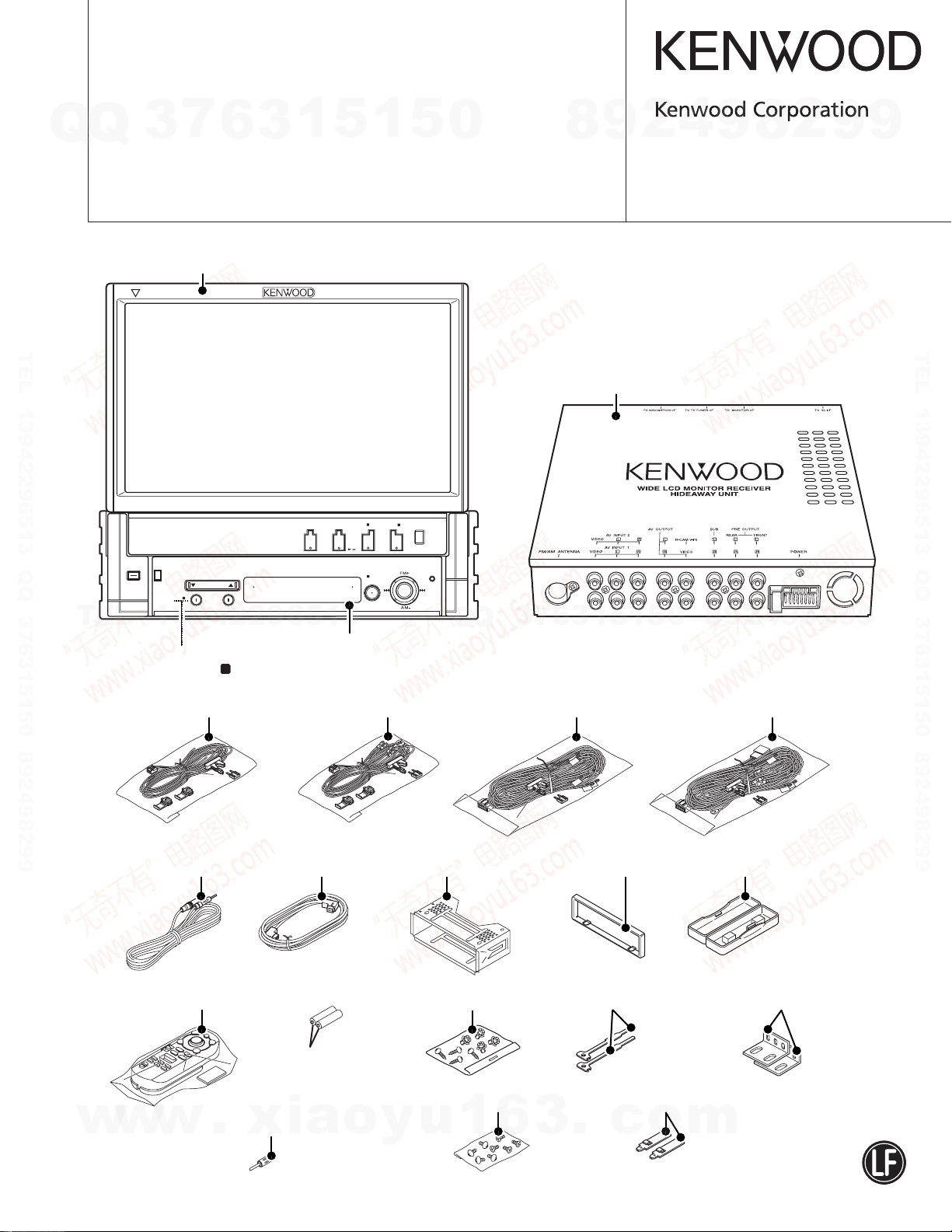
TV RECEIVER
KVT-M707
Q
Q
7
3
6
KVT-M707Y
3
1
5
1
5
0
SERVICE MANUAL
Panel
Destination K (A64-3600-01)
Destination E (A64-3601-01)
TEL 13942296513 QQ 376315150 892498299
WIDE LCD MONITOR RECEIVER KVT-M707
V.SEL V.OFF
MODE
SCRN FNC AV OUT SEL
MVFS
OPEN/CLOSE
TEL
Destination K : ATT
Destination E : ATT TI
13942296513
DC cord (Destination K)
(E30-6479-15)
VOLUME
AUTOATT TI
KENWOODTOUCH SCREENCONTROL
Panel assy
Destination K (A64-3568-02)
Destination E (A64-3569-02)
OFF
SRC
Q
Q
DC cord (Destination E)
(E30-6480-15)
7
3
DC cord (Destination K)
(E30-6481-15)
9
8
Metallic cabinet
(A01-2866-01)
5
1
3
6
4
2
© 2005-8 PRINTED IN JAPAN
B53-0309-00 (N) 1548
0
5
1
9
2
9
8
DC cord (Destination E)
(E30-6482-15)
8
4
2
9
8
9
2
9
9
TEL 13942296513 QQ 376315150 892498299
9
Cord with plug
(E30-6483-05)
Remote controller assy (KNA-RC400)
(A70-2073-05)
w
w
w
Cord with plug
(E30-6486-05)
Size AAA battery
(Not supplied)
Antenna adaptor (Destination E)
(T90-0552-05)
.
xia
o
y
Mounting hardware assy
(J21-9823-03)
Screw set
(N99-1753-05)
Screw set (Destination K)
(N99-1775-05)
u
1
6
3
Escutcheon
(B07-3082-02)
Lever
(D10-4674-04) x2
Mounting hardware (Destination K)
(J21-9784-04) x2 (for TOYOTA car)
.
c
o
Plastic cabinet assy
(A02-2723-03)
Mounting hardware
(J22-0054-14) x2
m
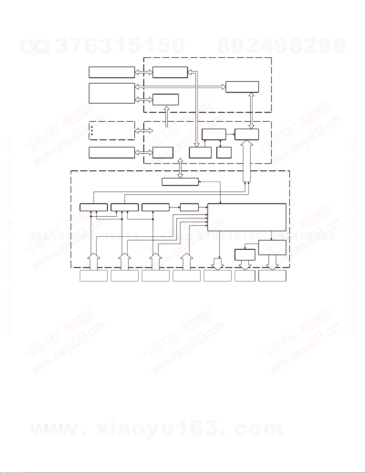
KVT-M707/M707Y
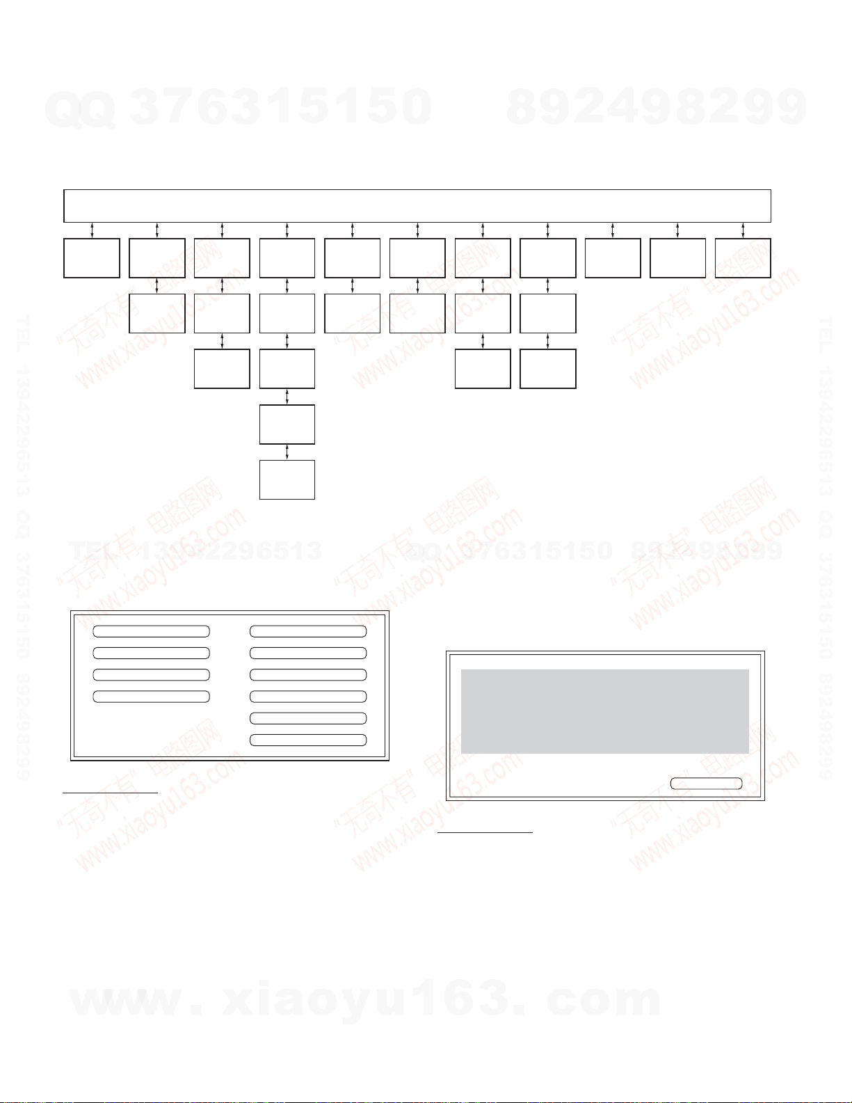
BLOCK DIAGRAM
7
Q
Q
TEL 13942296513 QQ 376315150 892498299
3
6
TOUCH PANEL
LCD
X16
SMALL DISPLAY
REMOTE CONTROL
KEY
SLIDE MECHA
X34
IC400-402
RGB SW VIDEO SW
3
IC406-408,
415,416
1
5
1
X35
Q501-503
TOUCH PANEL
CONTROL
IC1
INVERTER
CIRCUIT
X14
IC701,702
MOTOR
DRIVER
IC203,204
ISO AMP
5
0
IC303
TUNER u-COM
SYSTEM
u-COM ROM
IC413,414
MPX
IC301
OSD
IC151
9
8
IC101
TIMING
CONTROLLER
IC403
IC403IC103
OSD
AUDIO
INPUT SELECTOR
2
CHROMA
4
9
8
2
9
9
TEL 13942296513 QQ 376315150 892498299
TEL
13942296513
TV
INTERFACE
J502
NAVI AV-IN
INTERFACE INTERFACE INTERFACE
J503
J201
Q
Q
LX-BUS
J500
7
3
AV-OUT
INTERFACE
J202
6
3
0
5
1
5
1
IC100
POWER
AMP
SP OUTJ1PRE OUT
IC151
8
AUDIO
OUTPUT
SELECTOR
J200
9
2
4
9
8
2
9
9
2
w
w
w
.
xia
o
y
u
1
6
3
.
c
o
m

KVT-M707/M707Y
COMPONENTS DESCRIPTION
7
Q
Q
● VIDEO CONTROL UNIT (X14-954x-xx)
TEL 13942296513 QQ 376315150 892498299
TEL
w
3
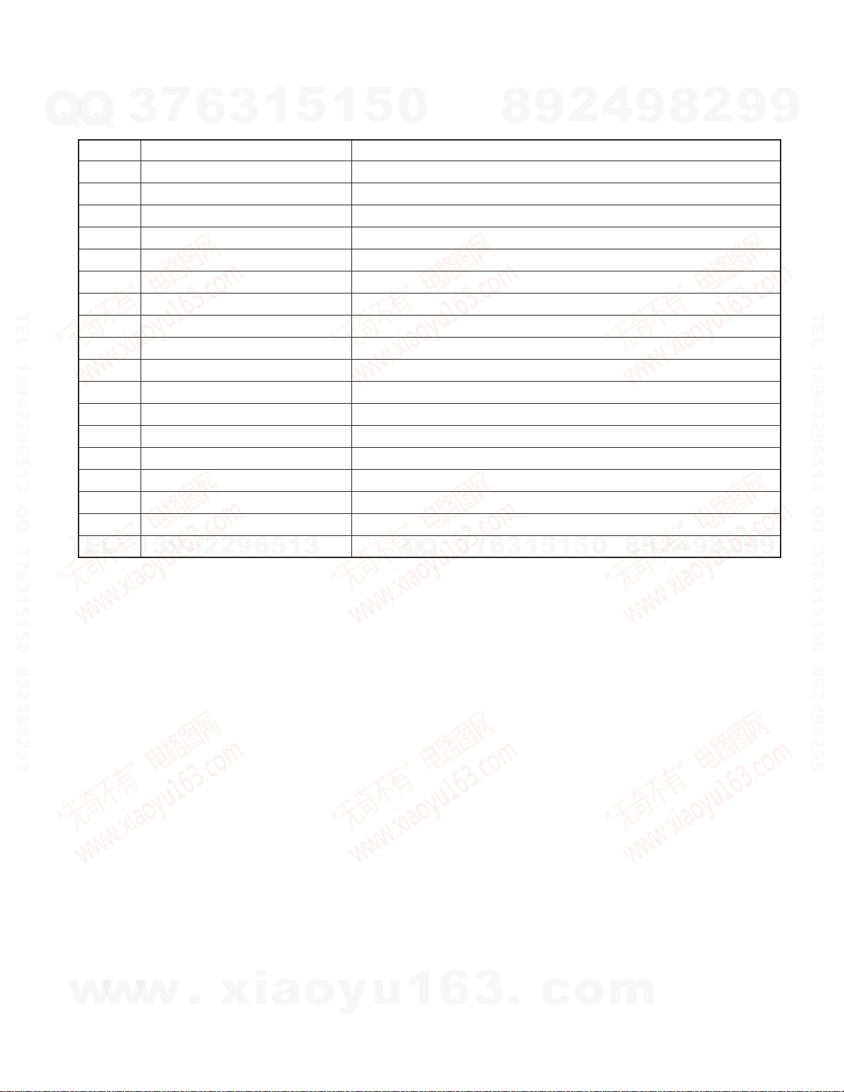
Ref. No. Application / Function Operation / Condition / Compatibility
IC1 DC-DC CONTROLLER DC-DC circuit control/driving
IC2 5V REGULATOR Power supply for BU5.0V
IC3 3.3V REGULATOR Power supply for P-ON 3.3V
IC101 E2PROM Non-volatile memory
IC103 SYSTEM µ-COM System control
IC104 RESET IC For resisting µ-com
IC105 AND Remote controller and wired remote controller
IC301 OSD IC IC for OSD display
IC303 OSD ROM ROM for OSD display
IC304 INVERTER For amplifying OSD clock
IC305 4-BIT COUNTERS PLL CLK 3-way divider circuit
IC306 AND PLL CLK 3-way divider circuit
IC307 NOR PLL CLK 3-way divider circuit
IC308 INVERTER PLL CLK 3-way divider circuit
IC401 MONO MULTI For γ IC HSYNC pulse width control
IC402 INVERTER For γ IC HSYNC pulse reversal
IC403 CHROMA/GAMMA IC Video signal processing for TFT liquid crystal
IC502 AND HSYNC buffer
IC503 SYNC SEPARATOR Synchronization separation
IC504 MONO MULTI HSYNC pulse width control for OSD IC
IC505 NON INVERTER SYNC buffer
IC506 NON INVERTER SYNC buffer
IC507 INVERTER For reversal of OSD IC HSYNC pulse
IC508 NAND VSYNC delay
IC510 AND 3.3V → 5.0V conversion
IC513 D FLIP-FLOP For HSYNC/VSYNC phase matching
IC514 3-STATE BUFFER For NTSC/PAL VSYNC switching
IC519 AND 3.3V → 5.0V conversion
IC522 EXCLUSIVE OR Separate synchronization signal → Compound synchronization signal conversion
IC701 MOTOR DRIVER For action mechanism sliding
IC702 MOTOR DRIVER For action mechanism tilting
Q1 SW SW for P-ON
Q3 SW For PARKING DET
Q5 SW For ACC DET
Q7 SW For software starting
Q9 SW SW for P-ON
Q10~12 SW For BU DET
Q13 BUFFER For switching transistor gate drive
13942296513
w
w
6
.
xia
3
1
5
o
1
y
5
u
0
Q
Q
1
3
6
7
3
6
8
3
.
9
1
1
5
c
2
5
o
4
0
m
9
8
9
8
2
4
2
9
8
9
2
9
9
TEL 13942296513 QQ 376315150 892498299
9
3
KVT-M707/M707Y
COMPONENTS DESCRIPTION
7
Q
Q
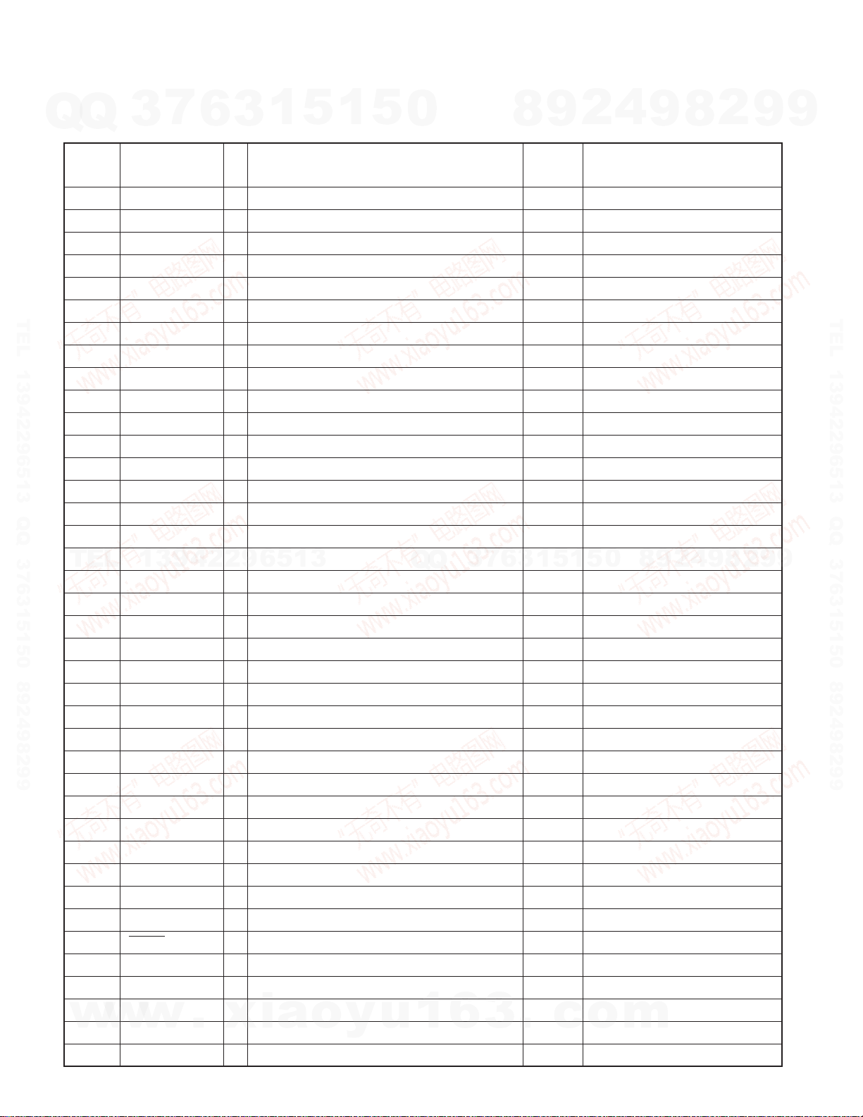
Ref. No. Application / Function Operation / Condition / Compatibility
Q14 SW For BU DET
Q15 BUFFER For switching transistor gate drive
Q16 SW For BU DET
Q17 POWER SUPPLY Switching transistor for flyback
Q18 SW For BU DET
Q19 POWER SUPPLY Switching transistor for voltage reduction chopper
Q20,21 SW For BU DET
TEL 13942296513 QQ 376315150 892498299
Q23 SW For REVERSE DET
Q25 POWER SUPPLY Power supply for 13.0V
Q26 SW For ILLUMI DET
Q27 POWER SUPPLY Power supply for 13.0V
Q30 SW Power supply for motor driver 5V ↔ 7.5V switching
Q35,36 POWER SUPPLY Power supply for 7.5V
Q37 SW For BU DET
Q103,104 SW For BLUE LED OFF/ON
Q105,106 SW For GREEN LED OFF/ON
Q107,108 SW For RED LED OFF/ON
Q109,110 SW For system RESET
Q120~122 SW For RED LED switching
TEL
Q304 BUFFER For OSD R signal
Q305 BUFFER For OSD G signal
Q306 BUFFER For OSD B signal
Q401 SW For NTSC/PAL chroma trap switching
Q402 SW For γ IC NTSC/PAL switching
Q403 BUFFER For VCOM signal
Q501 BUFFER Buffer for C-VIDEO
Q503 BUFFER Buffer for C-VIDEO
Q505 SW For NTSC/PAL VSYNC switching
Q507 BUFFER For γ R signal
Q508 BUFFER For γ G signal
Q509 BUFFER For γ B signal
3
13942296513
6
3
1
5
1
5
0
Q
Q
3
7
6
8
3
9
1
5
1
2
5
4
0
9
8
9
8
2
4
2
9
8
9
2
9
9
TEL 13942296513 QQ 376315150 892498299
9
● SUB-CIRCUIT UNIT (X16-3020-10)
Ref. No. Application / Function Operation / Condition / Compatibility
IC201 REMOTE Remote controller light receptor
Q101 DSI SIGNAL SW DSI signal control
Q206 LED SW LED Red or LED Green switching
w
w
w
4
.
xia
o
y
u
1
6
3
.
c
o
m

KVT-M707/M707Y
COMPONENTS DESCRIPTION
7
Q
Q
● ELECTRIC UNIT (X34-353x-xx)
TEL 13942296513 QQ 376315150 892498299
TEL
w
3
Ref. No. Application / Function Operation / Condition / Compatibility
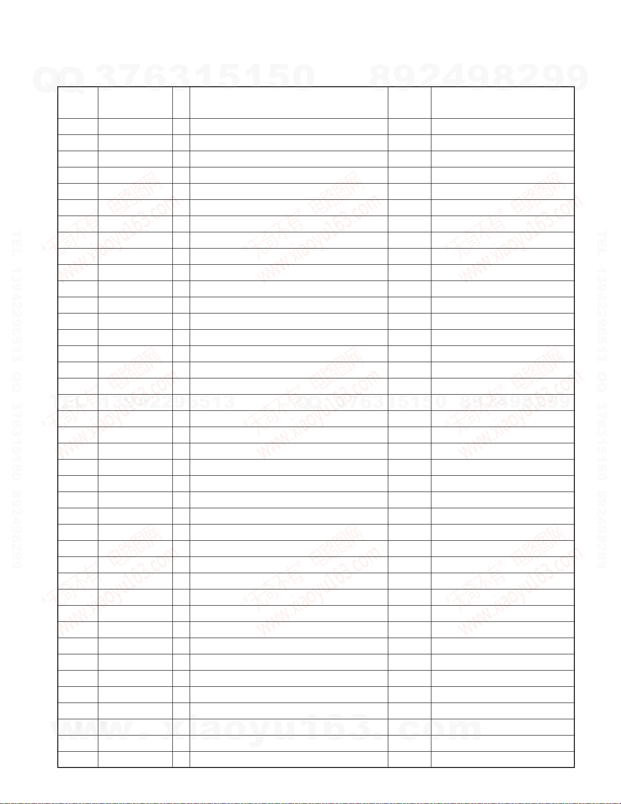
IC50 REGULATOR 8.4V for audio is generated from BU14V
IC52 POWER SUPPLY CONVERTER ±9.0V for 5V pre-out is generated from BU14V
IC54 REGULATOR 5V for video is generated from BU14V
IC100 POWER IC Power amplifier for speaker output
IC150 OP AMP Buffer for audio mid-point electric potential 3.3V and SVR voltage 6.8V
IC151 E-VOL / SELECTOR Audio volume control, audio signal selection
IC200 OP AMP For amplification of audio signal of 5V pre-out (Front)
IC201 OP AMP For amplification of audio signal of 5V pre-out (Rear)
IC202 OP AMP For amplification of audio signal of 5V pre-out (Sub-woofer)
IC203 ISO AMP For GND isolation of audio signal (AVIN2)
IC204 ISO AMP For GND isolation of audio signal (AVIN1)
IC251 RDS DECODER For RDS signal processing and demodulation
IC300 VOLTAGE DET For monitoring µ-com resetting voltage
IC301 NOR For MUTE control of audio
IC303 TUNER u-COM For controlling X34 board
IC400 VIDEO SW (R) For selection of video signal (R)
IC401 VIDEO SW (G) For selection of video signal (G)
IC402 VIDEO SW (B) For selection of video signal (B)
IC403 SYNC SEPARATOR For NTSC/PAL identification, AVIN and rear camera auto detection
IC404 VIDEO SW Video signal selection (For synchronization separation)
IC405 ISO AMP For GND isolation of audio signal (TV)
IC406,407 VIDEO SW Video signal selection (For monitoring the main unit)
IC408 VIDEO SW Video signal selection (For AV OUT)
IC413 MPX For selection of audio signal (MAIN source)
IC414 MPX For selection of audio signal (DUAL ZONE source)
IC415 VIDEO SW Video signal selection (For monitoring the main unit)
IC416 VIDEO SW Video signal selection (For AV OUT)
IC500 ISO AMP For GND isolation of audio signal (LX-BUS)
IC501 INVERTER For reversing reset signal
IC502 BUFFER Buffer for remote control signal to NAVI
IC504 OP AMP For DVD audio signal GND isolation (Right)
IC505 OP AMP For DVD audio signal GND isolation (Left)
Q1 FAN 11V Comes ON when Q2 is ON
Q2 FAN 11V Comes ON when Q3 is ON
Q3 FAN 11V Comes ON when SW5V is ON
Q4 FAN 11V For controlling output signal
Q6 ANT-CONT SW Comes ON when TUNER source is selected
Q7 P-CONT SW Comes ON when STANDBY source is selected
13942296513
w
w
6
.
xia
3
1
5
o
1
y
5
u
0
Q
Q
1
3
6
7
3
6
8
3
.
9
1
1
5
c
2
5
o
4
0
m
9
8
9
8
2
4
2
9
8
9
2
9
9
TEL 13942296513 QQ 376315150 892498299
9
5
KVT-M707/M707Y
COMPONENTS DESCRIPTION
7
Q
Q
Ref. No. Application / Function Operation / Condition / Compatibility
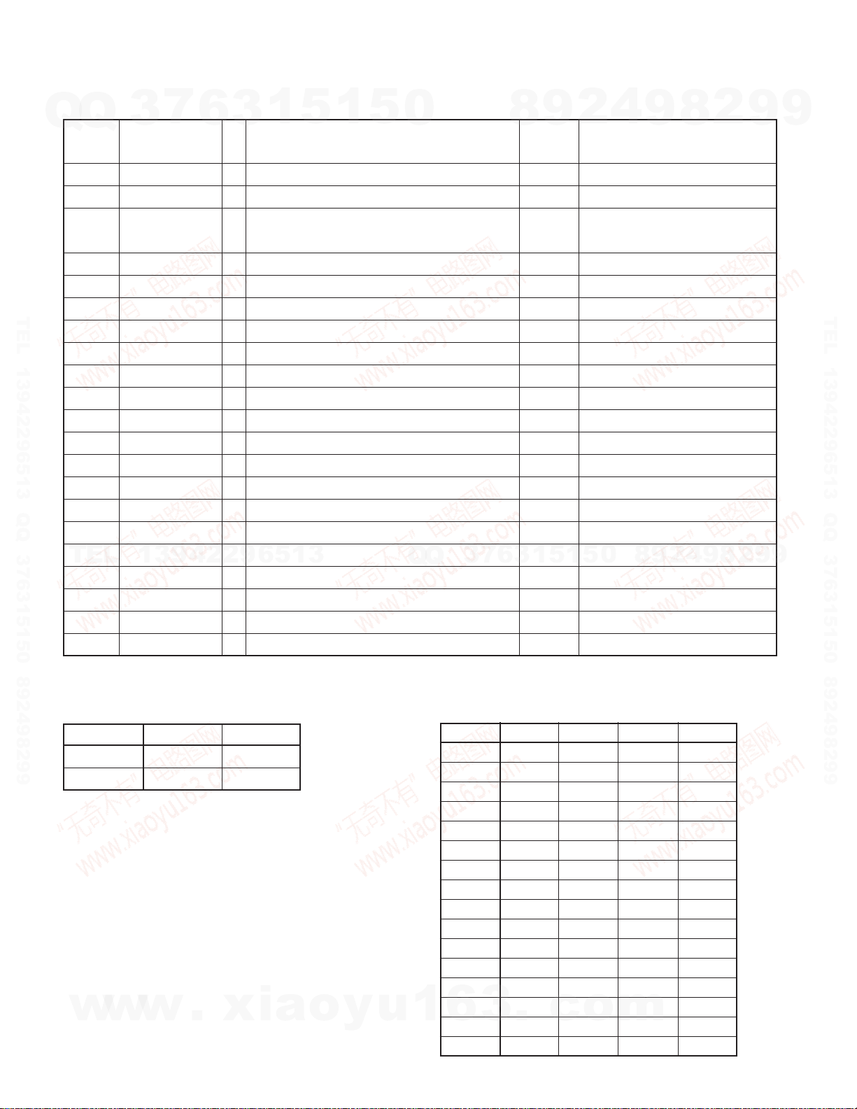
Q8~11 P-CONT CONTROL P-CONT circuit control
Q12 BU DET SW Comes ON when power supply voltage is about 8.8V or higher
Q13 EXT-AMP CONTROL External amp control
Q14 SURGE VOLTAGE DET Comes ON when Q15 is ON
Q15 SURGE VOLTAGE DET Comes ON when power supply voltage is about 20V or higher
Q50 ±9V POWER SUPPLY Comes ON when Q51 is ON
Q51 ±9V POWER SUPPLY Comes ON when SW14V is ON
TEL 13942296513 QQ 376315150 892498299
Q52 14V POWER SUPPLY SW Comes on at P-ON
Q54 BU5V POWER SUPPLY
Q55 A8V POWER SUPPLY SW Comes ON when SW14V is ON
Q58 BU5V POWER SUPPLY
Q59 A8V POWER SUPPLY BU14V → 8V for audio is supplied
Q61 V5V POWER SUPPLY SW Comes ON when SW14V is ON
Q62 SW5V POWER SUPPLY SW Comes on at P-ON
Q63 SW5V POWER SUPPLY BU5V → SW5 is supplied
Q64 V5V POWER SUPPLY BU14V → 5V for video is supplied
Q65~70 ±9V POWER SUPPLY
Q150
TEL
Q151
Q152
Q200 AUDIO MUTE Audio muting of pre-out front right channel
Q201 AUDIO MUTE Audio muting of pre-out front left channel
Q202 AUDIO MUTE Audio muting of pre-out rear left channel
Q203 AUDIO MUTE MUTE at momentary power down, reset, and audio MUTE timing
Q204 AUDIO MUTE Audio muting of pre-out rear right channel
Q205 AUDIO MUTE Audio muting of pre-out center channel
Q206 AUDIO MUTE Audio muting of pre-out sub-woofer channel
Q207 AUDIO MUTE Audio muting of AV OUT right channel
Q208 AUDIO MUTE MUTE at momentary power down, reset, and audio MUTE timing
Q209 AUDIO MUTE Audio muting of AV OUT left channel
Q250 AM POWER SUPPLY SW Comes ON at AM source selection
Q252 AM POWER SUPPLY Audio 8V is supplied at AM source selection
Q403,404 AUDIO SELECTOR COLTROL SW 5V → 8V conversion of IC413 µ-com control terminal voltage
Q405,406 AUDIO SELECTOR COLTROL SW 5V → 8V conversion of IC414 µ-com control terminal voltage
Q500 RESET SIGNAL VOLTAGE INVERTER Signal is reversed to obtain resetting signal to TV tuner.
3
SVR6.8V / AUD3.3V
IC150 POWER SUPPLY SW
13942296513
SVR VOLTAGE-DECREASED CONTROL
SVR6.8V / AUD3.3V
IC150 POWER SUPPLY SW
6
3
1
5
1
5
0
Comes ON when SW14V is ON
7
3
Q
Q
Electric current control of SVR voltage reduction circuit
Power supply to IC150, Voltage supply to Q151
6
8
3
9
1
5
1
2
5
4
0
9
8
9
8
2
4
2
9
8
9
2
9
9
TEL 13942296513 QQ 376315150 892498299
9
6
w
w
w
.
xia
o
y
u
1
6
3
.
c
o
m
KVT-M707/M707Y
COMPONENTS DESCRIPTION
7
Q
Q
● VIDEO UNIT (X35-4470-10)
TEL 13942296513 QQ 376315150 892498299
TEL
3
Ref. No. Application / Function Operation / Condition / Compatibility
IC1 INVERTER CONTROL Control and driving of inverter circuit for backlight
IC101 TIMING CONTROLLER LCD module control
IC205 3-STATE BUFFER Switch for start pulse switching
IC303 PLL LPF LPF for PLL control (VT voltage control)
IC401 DIMMER SENSOR Detection sensor for auto dimmer
Q1 DIMMER SW Goes ON/OFF by PWM control signal and put dimmer on backlight
Q2,3 INVERTER DRIVER Driving of inverter circuit
Q5 5V AVR 5V power supply for inverter control IC
Q100 SW OPEN/CLOSE key ILLUMI blinking switch
Q101,102 POWER SUPPLY Power supply for timing controller PLL circuit (17.5V)
Q104 VCO For PLL oscillation
Q105,106 POWER SUPPLY Power supply for timing controller PLL circuit (17.5V)
Q203 BUFFER Buffer for PLL clock
Q204 SW For switching IC205
Q205 SW Switch for compound synchronization/separation synchronization
Q501 TOUCH PANEL Y1 SW Comes ON at Y0 (X0) SW: Y (X)-axis input and goes OFF X (Y) axes input
Q502 TOUCH PANEL X0/Y1 SW Goes ON at Y1 SW: Y-axis input and impresses voltage
Q503 TOUCH PANEL X1/Y0 SW Comes on at X1 SW: panel touch detection or X-axis input and impresses voltage
13942296513
6
3
1
5
1
5
0
Q
Q
3
7
6
8
3
9
1
5
1
2
5
4
0
9
8
9
8
2
4
2
9
8
9
2
9
9
TEL 13942296513 QQ 376315150 892498299
9
w
w
w
.
xia
o
y
u
1
6
3
.
c
o
m
7
KVT-M707/M707Y
MICROCOMPUTER’S TERMINAL DESCRIPTION
7
Q
Q
● SYSTEM µ-COM : IC103 on X14- (VIDEO CONTROL UNIT)
Pin No. Pin Name I/O Application
1 OSD DATA O Data to OSDC-IC
2 OSD CLK O Clock to OSDC-IC
3NC 4SDA I/O Data to EEPROM
5NC -
TEL 13942296513 QQ 376315150 892498299
6 SYS SDATA I Data from TUNER µ-com
7 SYS MDATA O Data to TUNER µ-com
8 SYS MCLK O Clock to TUNER µ-com
9 EVDD 10 EVSS 11 NC 12 PON O Power supply ON/OFF control H: ON
13 REMO I Remote controller input
14 REVERSE I Reverse detection L: Reverse
15 HD IN I For γ automatic control / For PWM synchronization
16 γ DATA O Data to Chroma IC
17 γ CLK O Clock to Chroma IC
TEL
18 PWM O Light adjustment of backlight
19 MCNT O 7.5V power supply voltage control L: 5V, H: 7.5V
20 P DET O For control of power supply protection circuit H: ON
21 FROM VPP - Used at time of writing to flash ROM
22 DSI O LED control for DSI H: Light ON
23 ILL R O ILLUMI (Red) control H: Light ON
24 ILL G O ILLUMI (Green) control H: Light ON
25 ILL B O Sub-panel backlight (Blue) control H: Light ON
26 STATUS0 O For TV mechanism testing
27 EEPROM WRT I Write detection at ROM correction
28 TYPE0 I Destination setting q Refer to Truth Value Table
29 TYPE1 I Destination setting q Refer to Truth Value Table
30 NTSC/PAL O NTSC/PAL switching H: PAL, L: NTSC
31 NAVI O For NAVI synchronization switching At NAVI (RGB) display: L
32 OSD CS O Chip select to OSDC-IC
33 OSD RST O Reset to OSDC-IC L: RESET
34 RESET I
35 XT1 36 XT2 37 REGC -
w
38 X2 39 X1 -
8
3
13942296513
w
w
6
.
xia
3
1
5
o
1
y
5
u
0
Q
Q
1
3
6
7
3
8
6
9
Truth V alue
Table
1
3
.
4
2
Processing Operation Description
8
0
5
1
5
H: E2PROM write from outside, L: Other
c
o
m
9
9
8
2
4
2
9
8
9
2
9
9
TEL 13942296513 QQ 376315150 892498299
9
KVT-M707/M707Y
MICROCOMPUTER’S TERMINAL DESCRIPTION
7
Q
Q
TEL 13942296513 QQ 376315150 892498299
TEL
w
3
Pin No. Pin Name I/O Application
40 VSS 41 VDD 42 CLKOUT - NC
43 SYS ON O ON/OFF control to Tuner µ-com (X34-) H: ON, L: OFF
44 SYS MREQ O Request to Tuner µ-com (X34-)
45 SYS SREQ I Request from Tuner µ-com (X34-)
46 γ CS O Chip select to Chroma IC
47 VMUTE O Video mute H: MUTE ON
48 BL DET I Measure for backlight not lighting
49 RGB SW O Video source switching
50 LED SW O Blinking control of monitor OPEN/CLOSE key H: Light ON, L: Light OFF
51 ZOOM O Aspect setting r Refer to Truth Value Table
52 SIDE1 O Aspect setting r Refer to Truth Value Table
53 HPOS1 O Display start position setting we Refer to Truth Value Table
54 HPOS2 O Display start position setting we Refer to Truth Value Table
55 HPOS3 O Display start position setting we Refer to Truth Value Table
56 HPOS4 O Display start position setting we Refer to Truth Value Table
57 T/C RST O Resetting for timing controller L: RESET
58 BVDD 59 BVSS 60 MIRROR O Screen display right/left reversal H: Normal, L: Reverse
61 JUST O Aspect setting r Refer to Truth Value Table
62 X0 O Touch panel control y Refer to Truth Value Table
63 X1 O Touch panel control y Refer to Truth Value Table
64 Y0 O Touch panel control y Refer to Truth Value Table
65 ENABLE O Backlight power supply ON/OFF control H: ON, L: OFF
66 SW A I TV mechanism sliding detection
67 SW B I TV mechanism sliding detection
68 SW C I TV mechanism sliding detection
69 SW D I TV mechanism sliding detection
70 TMOTOR M O Motor control for TV mechanism (Tilt)
71 TMOTOR P O Motor control for TV mechanism (Tilt)
72 SMOTOR M O Motor control for TV mechanism (Slide)
73 SMOTOR P O Motor control for TV mechanism (Slide)
74 AVDD 75 AVSS 76 AVREF 77 LCD B I For γ automatic adjustment
78 LCD G I For γ automatic adjustment
79 LCD R I For γ automatic adjustment
13942296513
w
w
6
.
xia
3
1
5
o
1
y
5
u
0
Q
Q
1
3
6
7
3
6
8
3
.
9
Truth V alue
Table
1
5
1
c
4
2
5
o
0
9
Processing Operation Description
2
9
8
m
8
4
2
9
8
9
2
9
9
TEL 13942296513 QQ 376315150 892498299
9
9
KVT-M707/M707Y
MICROCOMPUTER’S TERMINAL DESCRIPTION
7
Q
Q
Pin No. Pin Name I/O Application
80 VCOM IN I For γ automatic adjustment
81 AUTO DIM I Auto dimmer
82 KEY1 I
83 XDATA I Touch panel input (X-direction)
84 YDATA I Touch panel input (Y-direction)
TEL 13942296513 QQ 376315150 892498299
85 PH DET I TV mechanism slide photo detection
86 R SENS I TV mechanism tilt sensor voltage detection
87 KEY2 I Sub-panel key (9 parts)
88 NC 89 PAK DET I Parking detection
90 ACC DET I ACC detection L: A CC ON
91 BU DET I Backup reduced electricity detection H: Momentary power down
92 ILLUMI DET I ILLUMI detection L: ILLUMI ON
93 VD IN I For γ automatic adjustment / PWM synchronization
94 OPEN CLOSE I OPEN/CLOSE key L: Key depressed
95 PANEL DET I Front panel detach/attach detection L: Attach, H: Detach
96 SRC I Source select key L: Key depressed
TEL
97 FLASH SI I Used at time of writing to flash ROM
98 FLASH SO O Used at time of writing to flash ROM
99 FLASH CLK O Used at time of writing to flash ROM
100 SCL I/O Clock for EEPROM
3
13942296513
6
1
5
1
3
Panel key (4 parts) switching of key processing in
synchronization with TV mechanism horizontal detection
5
0
Q
Q
3
7
8
6
9
Truth V alue
Table
1
3
4
2
Processing Operation Description
H: PARKING detection (When parking)
8
0
5
1
5
9
9
8
2
4
2
9
8
9
2
9
9
TEL 13942296513 QQ 376315150 892498299
9
Truth Value T able
q Destination Setting
Destination TYPE0 TYPE1
K10
E01
w
w
w
10
.
xia
o
y
u
w Horizontal Screen Position Adjustment
(In Test Mode, variable when adjusting horizontal screen position)
0.3125 HPOS1 HPOS2 HPOS3 HPOS4
+7 LO LO LO LO
+6 HI LO LO LO
+5 LO HI LO LO
+4 HI HI LO LO
+3 LO LO HI LO
+2 HI LO HI LO
+1 LO HI HI LO
0HIHIHILO
-1 LO LO LO HI
-2 HI LO LO HI
-3 LO HI LO HI
-4 HI HI LO HI
-5 LO LO HI HI
1
-6 HI LO HI HI
6
3
.
c
o
-7 LO HI HI HI
-8 HI HI HI HI
m
KVT-M707/M707Y
5.0V
A-D
XData
YData
µcom
Y0X0
X1
MICROCOMPUTER’S TERMINAL DESCRIPTION
7
Q
Q
e Screen Position Adjustment Value
TEL 13942296513 QQ 376315150 892498299
r Screen Mode Switching (Used at screen mode switching)
t Other control
TEL
*1: Right/Left reversal screen for back camera
*2: Timing controller RESET
*3: For NTSC/PAL switching
3
NTSC HPOS Default
Full OSD Lo, Lo, Lo, Lo 0
NAVI Lo, Lo, Lo, Lo 0
VD Lo, Lo, Lo, Lo 0
TV Lo, Lo, Lo, Lo 0
PAL NTSC+N HPOS Default
VD 0 Lo, Lo, Lo, Lo 0
TV 0 Lo, Lo, Lo, Lo 0
FULL LO LO LO
NORMAL LO LO HI
JUST LO HI HI
ZOOM HI LO LO or HI
MIRROR Right Left *1
13942296513
T/C RST OFF ON *2
NTSC PAL NTSC PAL *3
6
ZOOM JUST SIDE1
LO HI
3
1
5
1
5
0
Q
Q
y Touch Panel Control Timing
7
3
6
4
2
9
8
Detection
2.0msec
X1
X0
Y0
1
3
NO
Average except 3 bottom ones
Wait
2.0msec 2.0msec 2.0msec
Touch panel detection
Touch ON/OFF detection
xxV or more?
X-axis data read
Y-axis data read
0
5
1
5
Sampled for 5 times?
YES
8
YES
9
read
9
8
YDataXData
2
read
4
2
9
NO
8
9
2
9
9
TEL 13942296513 QQ 376315150 892498299
9
w
w
w
.
xia
End
o
y
u
1
6
3
.
c
o
m
11
KVT-M707/M707Y
MICROCOMPUTER’S TERMINAL DESCRIPTION
7
Q
Q
● TUNER µ-COM: IC303 on X34- (ELECTRIC UNIT)
Pin No. Pin Name I/O Application
1 TV CON O Startup request to TV unit H: TV unit ON, L: TV unit OFF
2 TUN SCL I/O Front-end I2C clock output terminal
3NAVI1 RX I Data from navigation 1
4NAVI1 TX O Data to navigation 1
5 VISUAL SW5 1 O TV/AVIN2 video switching !3 Refer to Truth Value Table
TEL 13942296513 QQ 376315150 892498299
6 EVDD 7 EVSS 8 RGB SW1 O TV/NAVI1/NAVI2 RGB video switching !0 Refer to Truth Value Table
9 RGB SW2 O TV/NAVI1/NAVI2 RGB video switching !0 Refer to Truth Value Table
10 VSYNC DET I
11 VISUAL SW4 O TV/Rear view camera video switching !2 Refer to Truth Value Table
12 SYS MDATA I Data from system control µ-com
13 SYS SDATA O Data to system control µ-com
14 SYS MCLK I Clock from system control µ-com
15 VSYNC SW1 O COMP signal for NTSC/PAL identification and !4 Refer to Truth Value Table
TEL
16 VISUAL SW3 2 O NAVI1/NAVI2/AVIN1video switching !1 Refer to Truth Value Table
17 PWIC BEEP O Beep output
18 IC/VPP 19 VISUAL SW3 1 O NAVI1/NAVI2/AVIN1 video switching !1 Refer to Truth Value Table
20 VISUAL SW2 2 O SW5 (or TV)/AVIN2/DVD video switching o Refer to Truth Value Table
21 VISUAL SW2 1 O SW5 (or TV)/AVIN2/DVD video switching o Refer to Truth Value Table
22 VISUAL SW1 2 O AVIN2/SW5 (or TV)/SW3 (or NAVI1) video switching i Refer to Truth Value Table
23 VISUAL SW1 1 O AVIN2/SW5 (or TV)/SW3 (or NAVI1) video switching i Refer to Truth Value Table
24 VISUAL SW5 2 O TV/AVIN2 video switching !3 Refer to Truth Value Table
25 RDS DATA I RDS decoder DATA input
26 RDS QUAL I RDS decoder QUAL input
27 P ON AM O AM power supply ON/OFF control
28 RDS AFS I/O Constant switching at noise detection
29 NC O
30 MUTE PRE O MUTE for PREOUT L: MUTE ON, H: Normal
31 RESET I
32 XT1 33 XT2 34 REGC -
w
35 X2 -
3
13942296513
w
w
6
.
xia
1
5
1
y
5
u
0
Q
Q
1
3
Vertical synchronization signal detection
(For AVIN2 automatic detection)
Switching for monitoring whether or not there is
COMP signal for AUTO detection
o
3
6
7
3
8
6
9
Truth V alue
Table
1
3
.
4
2
Processing Operation Description
8
0
5
1
5
H: ON (When AM selected), L: Normal
c
o
m
9
9
8
2
4
2
9
8
9
2
9
9
TEL 13942296513 QQ 376315150 892498299
9
12
KVT-M707/M707Y
MICROCOMPUTER’S TERMINAL DESCRIPTION
7
Q
Q
TEL 13942296513 QQ 376315150 892498299
TEL
w
3
Pin No. Pin Name I/O Application
36 X1 37 VSS 38 VDD 39 CLKOUT 40 MUTE AVOUT O MUTE for AV OUT L: MUTE ON, H: Normal
41 AUDIO SW1 A O
42 AUDIO SW1 B O
43 AUDIO SW2 A O TV/AVIN1/AVIN2 audio switching (for sub) w Refer to Truth Value Table
44 AUDIO SW2 B O TV/AVIN1/AVIN2 audio switching (for sub) w Refer to Truth Value Table
45,46 NC -
47 VSYNC SW2 O COMP signal for NTSC/PAL identification and !4
48 NC 49 P ON O SW5V → SW14V power supply ON/OFF control H: ON, L: Normal
50 ANT CONT O Power antenna control Antenna UP
13942296513
51 EXT CONT O External amp control
52 P CON O External amp power supply control ON at STANDBY): Hi
53 PWIC MUTE O POWER-IC MUTE control
54 PWIC STBY O POWER-IC standby control H: POWER ON, L: POWER OFF
55 BVDD 56 BVSS 57 NC 58 MUTE 0 O MUTE for IC2 VI OUT0 L: MUTE ON, H: MUTE OFF
59 MUTE 1 O MUTE for IC2 VI OUT1 L: MUTE ON, H: MUTE OFF
60 MUTE 2 O MUTE for IC2 VI OUT2 L: MUTE ON, H: MUTE OFF
61 TYPE4 I Destination setting u Refer to Truth Value Table
62 MUTE C O MUTE for IC2 V I MUX C L: MUTE ON, H: MUTE OFF
63 EEPROM SDA I/O Data for EEPROM (ROM correction)
64 EEPROM SCL I/O Clock for EEPROM (ROM correction)
65 LX CON O Startup request to slave unit H: Slave unit ON, L: Slave unit OFF
66 LX REQ M O Communication request to slave unit
67 LX MUTE I MUTE requests from slave unit H: MUTE ON, L: MUTE OFF
w
68 LX RST O Hard reset to slave unit H: Reset, L: Normal
w
6
.
xia
1
5
1
y
5
u
0
Q
Q
1
3
LX/NAVI1/SW3 (or TV)/AVIN1 audio switching (for main)
LX/NAVI1/SW3 (or TV)/AVIN1 audio switching (for main)
Switching for monitoring whether or not there is
COMP signal for AUTO detection
o
3
6
7
3
6
8
3
.
4
2
9
Truth V alue
Table
q Refer to Truth Value Table
q Refer to Truth Value Table
0
5
1
5
1
c
o
9
Processing Operation Description
Hi when FM/AM selection →
Other cases Low → Antenna DOWN
POWER ON (Power does not come
When STANDBY or POWER OFF: Low
L: MUTE ON (POWER, ACC OFF,
STANDBY, at momentary power down)
8
9
m
8
2
4
2
9
8
9
2
9
9
TEL 13942296513 QQ 376315150 892498299
9
13
KVT-M707/M707Y
MICROCOMPUTER’S TERMINAL DESCRIPTION
7
Q
Q
Pin No. Pin Name I/O Application
69 SYS MREQ I Request from system µ-com
70 SYS SREQ O Request to system µ-com
71 AVDD 72 AVSS 73 AVREF 74 DC ERR I DC offset error detection Low at detection
TEL 13942296513 QQ 376315150 892498299
75 LINE MUTE I LINE MUTE detection
76 TYPE2 I Destination setting u Refer to Truth Value Table
77 TYPE1 I Destination setting u Refer to Truth Value Table
78 TYPE0 I Destination setting u Refer to Truth Value Table
79 OEM TYPE1 I OEM destination setting y Refer to Truth Value Table
80 OEM TYPE0 I OEM destination setting y Refer to Truth Value Table
81 EEPROM WRT I Write detection at ROM correction
82 TYPE3 I Destination setting u Refer to Truth Value Table
TEL
83 TUN IFC OUT I Front-end IFC OUT input terminal H: With station, L: Without station
84 TUN SMETER I S-meter input
85 RDS NOISE I FM noise detection
86 TV SDATA I Data from TV unit
87 BU DET I Backup reduced electric power detection
88 LX REQ S I Communication request from slave unit
89 SYS ON I ON/OFF control from system control µ-com H: X34 Unit ON, L: X34 Unit OFF
90 TV SREQ I Request from TV unit
91 TV MDATA O Data to TV unit
92 TV MREQ O Request to TV unit
93 RDS CLK I RDS decoder CLK input
94 LX DATA S I Data from slave unit
95 LX DATA M O Data to slave unit
96 LX CLK I/O LX BUS clock
97 NC 98 TV JUDGE I TV tuner old/new identification H: Old, L: New
99 TV CLK O Clock to TV unit
100 TUN SDA I/O Front-end I2C data input/output terminal
3
13942296513
6
3
1
5
1
5
0
Q
Q
3
7
8
6
9
Truth V alue
Table
1
3
4
2
Processing Operation Description
Normal: 1.6V, TEL MUTE: 1V or lower
NAVI MUTE: 2.5V or higher
When writing to E2PROM from outside,
Hi input with a jig (Common use SCL
and SDA stop operation)
In other cases, Low (Pull-down)
8
0
5
1
5
With 8.8V or more: Low
At reduced electricity (8.8V or less ): Hi
9
9
8
2
4
2
9
8
9
2
9
9
TEL 13942296513 QQ 376315150 892498299
9
14
w
w
w
.
xia
o
y
u
1
6
3
.
c
o
m
KVT-M707/M707Y
MICROCOMPUTER’S TERMINAL DESCRIPTION
7
Q
Q
Truth Value T able
q Audio Selector 1 (IC413)
* Input is reversed by transistor before entering selector.
TEL 13942296513 QQ 376315150 892498299
w Audio Selector 2 (IC414)
* Input is reversed by transistor before entering selector.
y Destination setting for OEM
TEL
u TYPE4, TYPE3, TYPE2, TYPE1, TYPE0
Destination
i Video Selector 1 (IC407)
3
AUDIO SW1 A AUDIO SW1 B Output
LLIN3 AVIN1
HLIN2 TV
LHIN1 AVIN2
HHIN0 LX
AUDIO SW2 A AUDIO SW2 B Output
LLIN3 AVIN2
HLIN2 AVIN1
LHIN1 TV
HHIN0 Not used
Destination TYPE0 TYPE1
KENWOOD brand 0 0
13942296513
OEM1 0 1
OEM2 1 0
Test when driving in EU 1 1
TYPE4 TYPE3 TYPE2 TYPE1 TYPE0
K10001
E10010
VISUAL SW1 1 VISUAL SW1 2 Output
LLIN1 AVIN1
HLIN2 SW4
L/H H IN3
6
3
1
5
1
5
SW3 (or NAVI1)
0
Q
Q
!0 RGB SW (IC400-402)
RGB SW1 RGB SW2 Output
!1 Video Selector 3 (IC406)
VISUAL SW3 1 VISUAL SW3 2 Output
!2 Video Selector 4 (IC415)
VISUAL SW4 Output
!3 Video Selector 5 (IC416)
VISUAL SW5 1 VISUAL SW5 2 Output
7
3
!4 VSYNC selector (IC404)
VSYNC SW1 VSYNC SW2 Output
About muting of composite signal to X14
• Video Selector 1 is set to SW3 and Video Selector 3 is set
to MUTE. MUTE timing is at full OSD.
4
2
9
8
LLIN1 NAVI
HLIN2 TV
L/H H IN3 MUTE
LLIN1 NAVI1
HLIN2 AVIN2
LHIN3 Not used
HHMUTE -
L IN1 TV
H IN2 Rear view
0
5
1
5
1
3
6
LLIN1 TV
HLIN2 AVIN2
LHIN3 Not used
HHMUTE -
LLIN1 AVIN2
HLIN2 CAMERA
LHIN3 AVIN1
HHMUTE -
9
8
9
2
8
4
2
9
8
9
2
9
9
TEL 13942296513 QQ 376315150 892498299
9
o Video Selector 2 (IC408)
VISUAL SW2 1 VISUAL SW2 2 Output
LLIN1 AVIN1
HLIN2 SW5 (or TV)
w
L/H H IN3 DVD
w
w
.
xia
o
y
u
1
6
3
.
c
o
m
15

KVT-M707/M707Y
TEST MODE
7
Q
Q
● How to enter the test mode
While pressing [SRC] key and [ATT] key at the same time,
reset the unit.
Note: In the test mode, power supply is cut off after 30 minutes. (This is for making the operation possible without Security input even when the security is On.)
● Adjustment items
Items to be adjusted after writing on the EEPROM on which
TEL 13942296513 QQ 376315150 892498299
regions have been written.
As for the details of the adjustments, ref er to each adjustment
item.
• Service Information / Serial Code writing
• Chroma adjustment
• Writing Touch Adjust values
• Screen position adjustment
• Writing Security Code (Destination E only)
● How to clear the Security Code
In adjusting K destination units, if the unit starts up with Security ON, the Security Code can be cleared in the following
manner. (Other than in Test Mode)
1)In the e Security ON condition, after resetting or turning
TEL
power ON after backup OFF, then the session starts with
Security Code Input screen.
2)With the attached remote controller in the Audio SW selected condition, input the code with the following procedure.
Procedure 1: “K” input (Press Ten key [5] 2 times)
Procedure 2: “C” input (Press Ten key [2] 3 times)
Procedure 3: “A” input (Press Ten key [2] once)
Procedure 4: “Q” input (Press Ten key [7] 2 times)
3)Security Code is complete when the input screen for the
Security Code is cleared.
● Information Screen
Below are display contents of the Information Screen.
• Serial No.
• System µ-Com Version / ROM Correction Version / Type
• OSD Version
•Tuner µ-Com V ersion / R OM Correction V ersion / Type / Span
w
(Tuner frequency Span information)
• DC Offset detection information
16
3
13942296513
Note: If a remote controller other than the attached is
used, Pressing Tenkey [7] twice will cause “R” to be input.
If a mistake is made during Procedure 1~4 above, input
other remote controller Key. Then, start inputting again
from Procedure 1.
w
w
6
.
xia
3
1
5
o
1
y
5
u
0
• Security Info (BLANK: E2PR OM not written, ON/OFF: Normal condition (ON/OFF security is set), ERROR: E2PROM
write abnormal)
● TOUCH Screen
• Adjust Touch position and write it on E2PROM.
• With 3-point input, write from system µ-com to EEPROM is
achieved.
• E2PROM normal/abnormal ending is displayed on screen.
● HPOSI Screen
• Screen position adjustment is conducted and the result is
stored in E2PROM.
Adjustments are conducted in the following order:
Graphic → TV → VIDEO → NAVI
• DVD wallpaper is NTSC-fixed.
• E2PROM write normal/abnormal ending is displayed on
screen.
• While adjustment is conducted on DVD, TDV-540A (Title 3Chapter 16) is played.
After Disc Loading, by pressing Ten key [4] on the remote
controller, transition is made to Title 3-Chapter 16.
7
3
Q
Q
● SERVICE Screen
Shown below are contents of the Service Screen.
• Power On time
• Monitor Open number of times / Monitor Close number of
times
• E2PROM Chroma data information
• DC Offset detection information
Writing Serial No.
By pressing the Serial key, transition to the Serial No. Input
screen is made.
E2PROM Chroma Data Clear
By pressing the Clear key, the E2PROM Chroma data is
cleared.
DC Offset Data Clear
By pressing the Clear key, the E2PROM DC Offset data is
cleared.
● Chroma Screen
• Chroma adjustment is conducted and the result is stored in
E2PROM.
• The setting procedures are conducted with a remote controller.
• Chroma IC adjustment screen (Item setting) → To be writ-
1
ten on EEPROM.
6
3
Setting item: COM DC (00h~FFh)
6
8
3
.
9
1
1
5
c
2
5
o
4
0
m
9
8
9
8
2
4
2
9
8
9
2
9
9
TEL 13942296513 QQ 376315150 892498299
9
KVT-M707/M707Y
TEST MODE
7
Q
Q
• E2PROM write normal/abnormal ending is displayed on
•Writing region does not clear EEPROM Chroma data.
● Chroma Auto Screen
• Automatic Chroma adjustment is conducted and the result
TEL 13942296513 QQ 376315150 892498299
• E2PROM write normal/abnormal ending is displayed on
•Writing region does not clear EEPROM Chroma data.
● Chroma Func Screen
• Chroma adjustment is conducted and the result is stored in
• The setting procedures are conducted with a remote con-
TEL
3
screen.
EEPROM chroma data is cleared by the Clear key in the
Service screen.
is stored in E2PROM.
Automatic adjustment item: RGB Amplitude → Bright →
Ganma1 → Ganma2 → CONT RGB2 → SUB Br ight R →
SUB Bright B → COM Amplitude
screen.
EEPROM chroma data is cleared by the Clear key in the
Service screen.
E2PROM.
troller.
13942296513
6
3
1
5
1
5
0
Q
Q
• Chroma IC adjustment screen (Item Setting) → Write on
EEPROM.
• E2PROM write normal/abnormal ending is displayed on
screen.
•Writing region does not clear EEPROM Chroma data.
EEPROM Chroma data is cleared by the Clear key in the
Service screen.
● Source / Audio / Setup Screen
• Source / Audio Control / Setup Screen are the same as
normal condition.
● Display
• Basically , in the Test Mode, screen will be dedicated screen.
• There will be no opening screen.
• Even during seek, the frequency display will be made.
•Touch position display (+) will be made. However, no display will be made in the Touch Adjust screen (In adjustment).
● Mini Liquid Crystal
7
3
• When starting up in the Test Mode, all lights will be lighted.
• All lighted condition will be released by Disp key.
4
2
9
8
Setting Item: Tint adjustment (00h~FFh)
Phase adjustment (00h~FFh)
8
0
5
1
5
1
3
6
9
9
8
2
4
9
2
8
9
2
9
9
TEL 13942296513 QQ 376315150 892498299
9
● Key
• Tact Key specifications are shown below.
1DIN (UNIT SP) 1DIN (BOX SP) 2DIN
SRC As usual As usual As usual
Vol Up As usual As usual As usual
Vol Down As usual As usual As usual
Track (Seek) Up As usual As usual As usual
Track (Seek) Down As usual As usual As usual
Disc (FM+/Band) Up As usual As usual Disc (AM-/M·S) Down As usual As usual AUTO (TI/DISP)
With mini liquid crystal Press more than 1 sec.: Motor Press more than 1 sec.: Motor driver
AUTO (TI/DISP)
Without mini liquid crystal Press more than 1 sec.: Motor
ATT As usual Flicker adjustment As usual
Screen As usua As usual As usual
Mode As usua As usual As usual
V.SEL V.SEL + AV OUT V.SEL + AV OUT V.SEL + AV OUT
w
w
FNC Normal (No Easy) Normal (No Easy) Normal (No Easy)
Open As usual As usual -
w
.
Press less than 1 sec.: NAVI forced interruption
Press less than 1 sec.: NAVI forced interruption
xia
o
y
u
1
Press less than 1 sec.: DISP -
Motor driver NAVI forced interruption
6
3
.
c
o
m
17
KVT-M707/M707Y
TEST MODE
7
Q
Q
● Remote Controller
• Using NA-R300 (SW: AUD), the following oper ations will be
conducted (Normal operation other than the following)
Key code Item
Direct Chroma IC adjustment mode ON/OFF (Write)
Band (FM+) Video mode switching (NAVI/AVIN/DVD)
M/S (AM-) DVD audio/video confirmation switching
Performance Chroma setting value set/release
TEL 13942296513 QQ 376315150 892498299
(Play/Pause)
Ten key 7 To previous item of chroma adjustment
Ten key 8 Chroma setting value change (UP)
Ten key 9 To next item of chroma adjustment
Ten key 0 Chroma setting value change (Down)
Ten key 1 DVD 5.1ch audio confirmation switching
(Preset 1) (DVD source only)
Ten key 2 DC Offset detection check direct switching
(Preset 2) (CD-CH source only)
Ten key 3 V-IN mirror mode switching
(Preset 3)
Ten key 4 HPOSI DVD confirmation direct switching
TEL
(Preset 4)
● Screen Management section
• While in the Test Mode (Including connection with special
µ-com/jig), the startup will be with VIDEO screen. → Transi-
tion to Test Mode Main screen is made with [FNC] key.
• In coordination with V.SEL, AV OUT is also switched. (AV
OUT with Graphic and NAVI can be anything.)
AVIN1 – (AVIN2) – (TV) – R-CAM – NAVI-DVD (NO specific
order)
• Easy Control screen can be skipped using [FNC] key.
• Parking detection is ignored in Test Mode. However, Parking is not ignored when Unit is special.
• Reverse condition occurring in Test Mode will be made On
condition (V.SEL always has R-CAM). However, when Unit
is special, it will be as usual.
(When detected, Reverse will cause R-CAM interruption,
as usual.)
• Default screen of System Setup will be made System 2.
• Default screen of Audio Setup will be made Speak er Setup .
• Default speaker selected of Speaker Setup will be made
Sub-woofer.
• When VIDEO 1 video is input or at signal switching (NTSC
↔ PAL) will not be OSD displayed. (OSD display will be
w
made at V.SEL switching. Display will not be made at the
time of VIDEO 1.)
18
3
13942296513
w
w
6
.
xia
3
1
5
o
1
y
5
u
0
● BEEP Control
• Beep will be sound regardless of destinations
(When Standby sourcing, Beep will not be sound as PWIC
limitation item.)
● DSI Control
• Default of DSI will be On.
● AVIF
•AVIN2 (AVIN1 for models with no AVIN2) Interruption will
be made default On.
• NAVI interruption SP setting will be default FRONT ALL.
• V-IN mirror mode switching will be conducted with remote
controller T enk ey [3].
• R-CAM Interruption will be made default On (Unit SP only).
● SCREEN Adjustment
• Default is center. With one click, Full Down ↔ Center ↔
Full Up.
• Default for BRT is MAX.
• The default for Auto Dimmer is Off and Dimmer Level 0.
Wait for switching detection will be cut.
7
3
Q
Q
● Audio
• Default for Volume is Step 30.
• Bal/Fad setting is 1 click: Min ↔ Center ↔ Max
• Default for Line Mute is On.
• X’over setting is 1 click: Min ↔ Max
• Tone setting is 1 click: Min ↔ Center ↔ Max
• Default for Tone (EQ) is Flat.
• Default for System Q is OFF.
• When equipped with Digital Out terminal, setting will be for
always output On.
● TUNER
• When E2PROM cannot be accessed, Error display will be
made. (Tuner screen)
• Forced Narrow/ Middle/ Wide switching of K3I.
By pressing more than 1 sec. on Preset 4
: Forced Narrow (∗∗∗.∗1MHz)
By pressing more than 1 sec. on Preset 5
: Forced Middle (∗∗∗.∗2MHz)
By pressing more than 1 sec. on Preset 6
: Forced Wide (∗∗∗.∗3MHz)
1
6
3
6
8
3
.
9
1
1
5
c
2
5
o
4
0
m
9
8
9
8
2
4
2
9
8
9
2
9
9
TEL 13942296513 QQ 376315150 892498299
9

KVT-M707/M707Y
TEST MODE
7
Q
Q
● Panel Mechanism
• At Full Open, angle is vertical and Slide is at the very back.
• Panel Mecha Slide/Angle will be in 3 steps.
• OPEN/CLOSE key illumination will blink all the time.
●Flicker Adjustment (When Hideaway Unit special
1)When ATT key is pressed, flicker adjustment comes On.
TEL 13942296513 QQ 376315150 892498299
2)When ATT key is pressed for the second time, flicker ad-
● DC Offset
• Clearing DC Offset detection (normal/abnormal)
• DC Offset detection information will be displayed on Infor-
TEL
• During Test Mode, even if DC Offset is detected, this will
• By pressing remote controller Tenkey 2 (Preset 2), the Vol-
3
connected)
Monitor is slid all the way to the front, the screen mode is
ZOOM, and Video Mode is VIDEO.
justment comes Off.
Monitor is slid is slid all the way to the back. (Initial position
of T est Mode.)
The screen mode is full and video will be the video changed
during adjustment.
By the use of DC Offset information clear key in the Service
Information Screen, DC Offset detection information on
E2PROM will be cleared.
13942296513
mation screen/Service Information screen.
not be written to E2PROM.
ume setting will be switched to the follo wing setting values.
Source: CD-CH
Designated disc: KTD-02A Designated
Track: 15 (20Hz, 0dB)
DISC/TRACK designation is conducted manually
Designated V ol: 29
6
3
1
5
1
5
0
Q
Q
● Specification to turn motor driver ON with no slide
mechanism
•In the condition where designation key is pressed down,
motor driver port is turned On.
With the [DISP] key depress, the motor is turned in forw ard
direction with the 1st key ON. With [DISP] key OFF, motor
stops.
With [DISP] key ON for the 2nd time, motor reverses. With
[DISP] key OFF, motor stops. This goes on thereafter.
● Backup Memory
• During the Test Mode, Backup Memory function does not
work.
● Clearing E2PROM contents
• E2PROM contents that should not remain at shipping is
cleared.
[SRC] key, [AUTO] key and Reset clears the memory content.
7
3
4
2
9
8
DC Offset information
Memory function
Storefront mode information
Service information
6
3
1
5
1
5
0
9
8
9
8
2
4
2
9
8
9
2
9
9
TEL 13942296513 QQ 376315150 892498299
9
w
w
w
.
xia
o
y
u
1
6
3
.
c
o
m
19
KVT-M707/M707Y
TEST MODE
7
Q
Q
Screen Specifications
• During the Test Mode, when Graphic Screen is selected,
Test Mode Main screen is displayed.
Information
sceen
TEL 13942296513 QQ 376315150 892498299
3
Service
screen
Writing for
Serial
number
6
Touch
screen
Touch
adjustment
1~3 points
EEPROM
Write
OK/NG
3
1
5
Hposi
screen
OSD
adjustment
TV
adjustment
NAVI
adjustment
EEPROM
Write
OK/NG
1
5
Test Mode Main screen
MECHA
ADJ
screen
EEPROM
Write
OK/NG
0
Chroma
screen
EEPROM
Write
OK/NG
Chroma
Auto
screen
Chroma
adjustment
EEPROM
Write
OK/NG
*1: Same as normal screen (Other than Test Mode)
8
adjustment
9
Chroma
Func
screen
Chroma
EEPROM
Write
OK/NG
2
4
Source
screen
*1
9
8
Set Up
screen
*1
2
9
Audio
screen
*1
9
TEL 13942296513 QQ 376315150 892498299
TEL
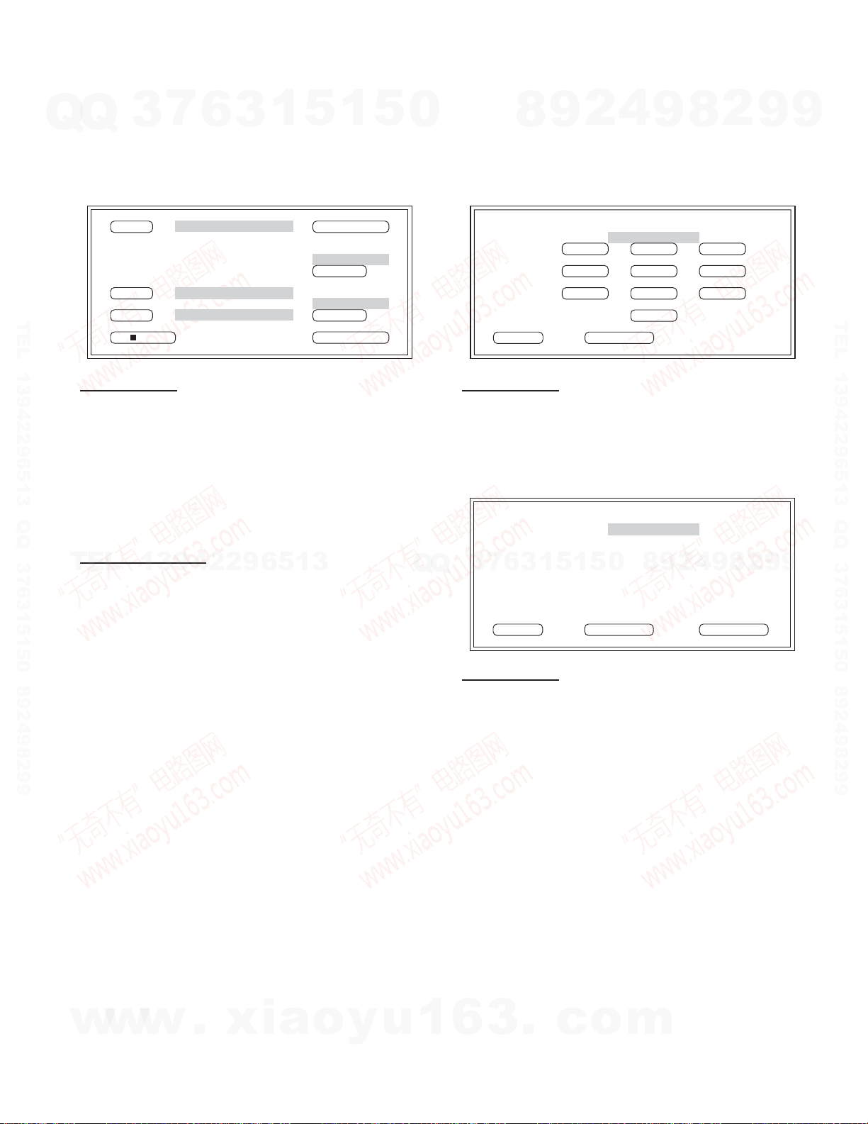
● Test Mode Main Screen
Test Mode Main
Key Specification
Information: Information Screen is displayed.
Service: Service Screen is displayed.
Touch: Touch Screen is displayed.
Hposi: Hposi Screen is displayed.
Source: Source Screen is displayed.
Set Up: Set Up Screen is displayed.
Audio: Audio Screen is displayed.
Chroma: Chroma Screen is displayed.
Chroma Auto: Chroma Auto Screen is displayed.
Chroma Func: Chroma Func Screen is displayed.
13942296513
Information
Service
Touch
Hposi
Source
Set Up
Audio
Chroma
Chroma Auto
Chroma Func
4
2
9
8
0
5
1
5
1
3
6
7
3
Q
Q
● Information Screen
• Serial No./µ-com v ersion information/V arious conditions, etc.
are displayed.
Serial:xxxxxxxx
DC Offset:None Security:Off
System Ver:4.XXX ROM:R––– Type:∗
OSD ROM Ver:1.15
Box Ver:4.XXX ROM:R––– Type:∗
Span:–
Return
Key Specification
Return: Test Mode Main Screen is displayed.
9
8
2
9
9
20
w
w
w
.
xia
o
y
u
1
6
3
.
c
o
m
KVT-M707/M707Y
TEST MODE
7
Q
Q
● Service Screen
• Service information is displayed/cleared.
• EEPROM Chroma data is cleared.
• DC Offset detection information is displayed/cleared.
TEL 13942296513 QQ 376315150 892498299
Key Specification
3
Init
Init
Init
Start
Init: Items to be initialized are selected.
■Start : Items that are selected with long-press (1 second
or more) are initialized.
Serial: Serial No Manual Input Screen is displayed.
Clear: EEPROM Chroma data is cleared.
Clear: EEPROM DC Offset information data is cleared.
Return: Test Mode Main Screen is displayed.
6
Power On ∗∗∗ hour
Mon. Open
Mon. Close
3
∗∗∗ time
∗∗∗ time
1
5
Chroma
DCOffset
1
Serial
Ready
Clear
None
Clear
Return
5
0
● Serial Number Input Screen
• The serial number for each set is written.
Serial Number Input Screen
Key Specification
0~9: Ten Key for Serial Number Input
Clear: Serial number being input is cleared.
Cancel : Service Screen is displayed.
Serial Number Input writing Screen
8
Clear
4
2
9
––––––––
1 2
4 5 6
7 8 9
Cancel
∗∗∗∗∗∗∗∗
9
0
8
2
3
9
9
TEL 13942296513 QQ 376315150 892498299
Adjustment Procedure
TEL
Service Information
• Select those items to be initialized by pressing Init K ey. (More
than 1 can be selected. / Those items that are selected are
focus displayed.)
• When selection is complete, press Start Key for 1 second
or more. The Service Information displayed is initialized.
Chroma
• Chroma information is normally Ready-displayed. When
EEPROM data is cleared, Clr OK/NG is displayed.
• At the time of Clear, if not reset, When Chroma Adjustment
Screen is displayed., the previous data is maintained. It is
only after resetting that the cleared data is reflected.
DC Offset
• As for DC Offset information, None means no detection and
Detect means information detected.
• With Clear key, detection information is cleared.
13942296513
Q
3
Q
Key Specification
Clear: Serial number being input is cleared.
Cancel: Service Screen is displayed.
Enter: Serial Number writing start (Write OK means normal
ending. write NG display means error. )
When OK, Service Screen is displayed with this key.
When NG, enter the Test Mode again, and re-do from the
beginning.
7
6
Clear
3
1
5
9
8
0
5
1
Cancel Enter
2
4
9
8
2
9
9
w
w
w
.
xia
o
y
u
1
6
3
.
c
o
m
21
 Loading...