Kenwood KVT-50-DVDRY, KVT-522-DVD, KVT-512-DVDRY, KVT-522-DVDY, KVT-532-DVD Service manual
...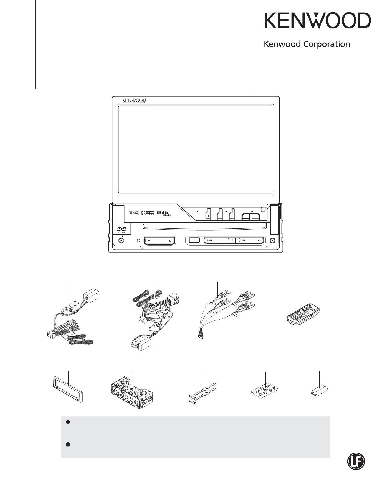
MONITOR WITH DVD RECEIVER
KVT-50DVDRY/512/522DVD
/522DVDY/532DVD/532DVDM
SERVICE MANUAL
© 2008-3 PRINTED IN JA PAN
B53-0621-00 (N) 519
DC cord *
(E30-6815-05)
ATT
TI
VOLUME
Illustrations is KVT-522DVD
DC cord *
(E30-6816-05)
OFF
SCAN
OPEN
/CLOSE
AUTO
Cord with plug
(E30-6813-05)
MONITOR WITH DVD RECEIVER
TEL
SF
+FM
V.OFF
SRC NAV
KVT-522DVD
EJECT
Remote controller *
(A70-2083-15)
REV: 5m
PRK: 2m
BU,GND: 1m
Escutcheon
(B07-3159-02)
Mounting hardware assy
(J21-9716-03)
The IC3, and IC11 in the DVD unit (X37-1100-03) are not replaceable components.
When these ICs are defective, replace the whole DVD mechanism assembly (X92-6160-00).
You cannot replace only the board.
TEST MODE is the same as DDX512.
Please refer to the service manual (DDX512: B53-0620-00).
* Depends on the models. Refer to the parts list.
Lever
(D10-4589-04) x2
This product complies with the
Screw set *
(N99-1758-15)
This product uses Lead Free solder.
RoHS directive for the European market.
RC-DV340
SIZE AAA BATTERY *
(NOT SUPPLIED)
KVT-50DVDRY/512/522DVD
/522DVDY/532DVD/532DVDM
CAUTIONS IN ASSEMBLING PANEL DRIVE MECHANISM (A10-5171)
Observe the instructions described in this document when
you are going to replace the parts or components that are
shown in this document.
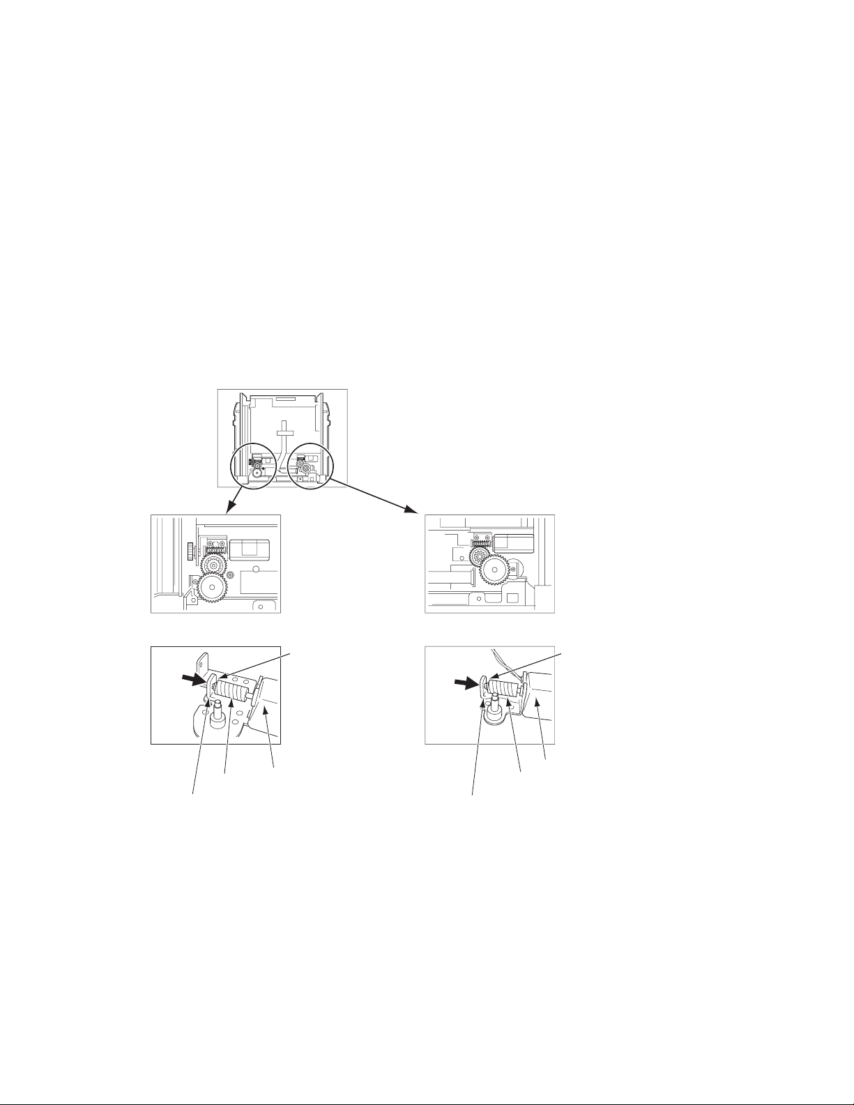
1. Replacement of motor fl at spring
• When mounting the flat spring that shall be in contact
with the worm gear, press the spring toward the direction
shown with an arrow so that there will be no gap be-
tween the tip of the gear and the spring and then mount
the spring. The gear shall be pressure-inserted into the
motor.
• Note that there are two motors. Above operation of
mounting the fl at spring is required on both of them.
Tilt drive gear train
Worm
Flat Spring
Mount the flat spring
while pressing it
towards the direction
shown with an arrow
so that there will be no
clearance.
DC Motor
Slide drive gear train
Mount the flat spring
while pressing it
towards the direction
shown with an arrow
so that there will be no
clearance.
DC Motor
Worm
Flat Spring
2
KVT-50DVDRY/512/522DVD
/522DVDY/532DVD/532DVDM
CAUTIONS IN ASSEMBLING PANEL DRIVE MECHANISM (A10-5171)
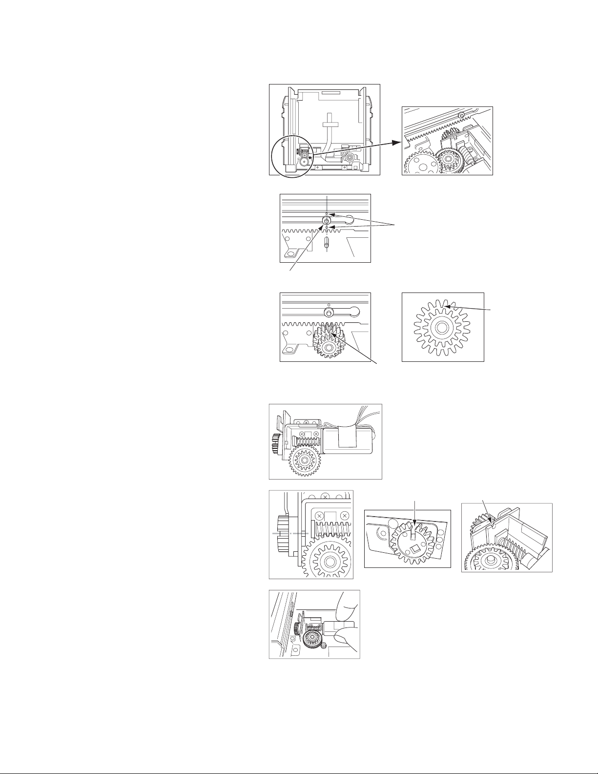
2. Phase matching among gears
• Monitor tilt is driven under the control of the
rotary sensor and the phase matching among
gears and sensor is required.
The procedure for the phase matching is de-
scribed in the rest of this subsection.
Tilt drive gear train
1) Align the mark on the rack with the pin. (When
the monitor is folded down at 0 degree, the
rack is located at the position where the mark
and pin are aligned.
T-Rack-A Pin
Location of mark
on the Rack
2) Insert the gear while keeping aligning the rack
pin with the notched section on the tilt gear 7.
3) Pre-assemble the tilt motor bracket assembly
(BKT Assy).
4) Align the notch on the sensor BKT with the
concave section of the sensor in the Assy.
Tilt Gear 7
Location of
notched section
Location of
notched section
Sensor Tilt Sensor Bkt
5) While keeping the conditions stated in 3) and
4), insert the tilt motor BKT Assy transversally,
and fi x the motor.
3
KVT-50DVDRY/512/522DVD
/522DVDY/532DVD/532DVDM
CAUTIONS IN ASSEMBLING PANEL DRIVE MECHANISM (A10-5171)
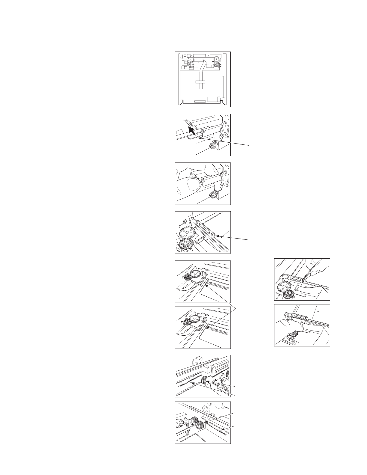
3. Insertion of slider
• This subsection describes cautions for inserting the
slider (slide section inside of the unit) into the outer
chassis.
1) On the rail at the left side of the slider, there is a part
called a stabilizer that is used to minimize play in
right and left sides.
The slide is made of resin. (Note that the rail is
shown at the right side of the slider in the picture.)
When inserting the slider, press the stabilizer towards
the direction shown with a blue arrow and insert it
into the groove on the rail.
2) PCB holder is pushed out towards the downside of
the picture due to the spring force and thus the chas-
sis and photo refl ection sheet may be get caught by
the holder during the assembly.
Insert the slider while slightly lifting up the holder with
a pair of tweezers or any other similar device.
(Slider -Slide section inside of the unit)
Stabilizer
PCB Holder
Hold and lift up the holder
with a pair of tweezers.
3) Insert the gear after confirming that the both of D
shaft gears at the right and left sides of the slider are
aliened with the tip of the right and left racks on the
chassis.
(Otherwise the slider will be inserted sidelong.
4
These portions
tend to be get
caught.
Push the opposite side of
the PCB holder towards
the downside of the picture
and lift up the portions
that may get caught.
D shaft gear
Rack gear
D shaft gear
Rack gear
KVT-50DVDRY/512/522DVD
/522DVDY/532DVD/532DVDM
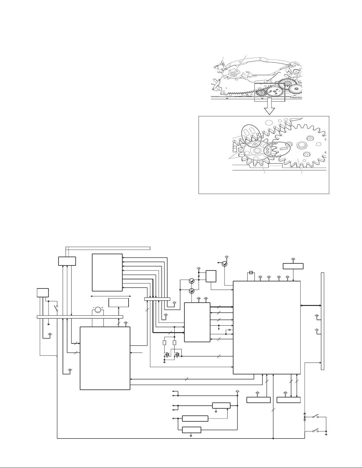
GEAR POSITION IN A DVD MECHANISM
In assembling the Traverse UD arm, Drive cam assembly,
Drive gear 5 and Drive gear 4C, align register marks on
these components.
BLOCK DIAGRAM
Inscriptions
(register marks)
on gears
Align 6 marks as
shown in the
figure
Traverse UD arm
Drive cam assembly
Drive gear 5
Do not forcibly press gears to engage their teeth
but freely let the gears fall under their own weight
and engage their teeth.
Drive gear 4C
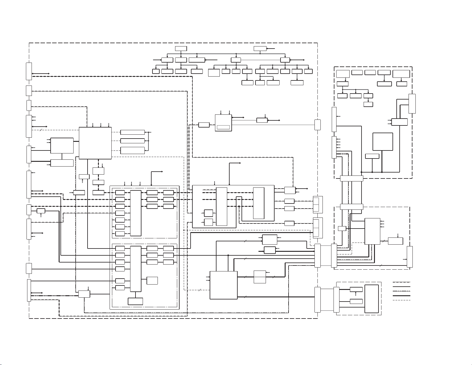
DVS-8000V BLOCK DIAGRAM (X37-1100)
SPINDLE
MOTOR
HALL
IC
HALL BIAS
U,V,W COIL
HALL SENSOR
LIM-SW
IC10
D3.3V
SW EJEND
P5V
3
3
H1H,H1L,HB
A1,A2,A3
DISC
OPTICAL PICKUP
LO/EJ
DC MOTOR
M
FO6,RO6
MOTOR &
ACTUATOR
DRIVER
2 PHASE
STEPPING
4
FO5,RO5
FO4,RO4
FO2,RO2
FO3,RO3
VREF,EC
STBY,SPIN,IN2-6
BMS,MUTE
PDIC VCC
DVD LD/CD LD
HFM
VREFH
IMON/VR DVD/VR CD
PDIC I/V OUT
THERMISTER
FO+/-,TR+/-
CN1
30PIN
4
CN3
28PIN
P5V
VHALF
FG
Q7,8
APC
Tr
A5V
IC1
FRONT-END
Q1,2
PROCESSOR
VREFH
LPC1,2
A,B,C,D,E,F,
RF,FE1,FE2
SEN,SCK,STDI
9
IC8
IC9
1.5V REG
HFM3.3V
9
VR
A5V
D5V
A3.3V
D3.3V
1.5V VOLTAGE DET
A5V
A5V
HFM3.3V
IC12
IOP
DET
A3.3V
2
3
7
VHALF
3
2
IC7
3.3V REG
ON/OFF
A3.3V
IC4
16.897849MHz
D5V A3.3V 1.5VD3.3V
HFM
IOP(AD)
ARF,NARF
FBAL,JLINE,
TSTSG
FE,AS,RFENV,RFDIFO
OFTR,BDO,VREF2
VHALF(1.65V)
TRCRS
TE
SEN,SCK,STDI
DVDON/
CDON
TEMP
DET(AD)
D5V
SPDRV,FODRV,
IC11
DRV.MUTE,LO.MTE,
TRDRV,PWM8,
D3.3V
RESET IC
NRST
OPTICAL DISC
CONTROLLER
FG,EXCNT1
SDA,SCL
BMS,STEP A,STEP B
SW
28
D3.3VD3.3V
IC3
FLASH ROMEEPROM
4
FADR0-17,
NCE,NWE,NOE
21
ATAPI IF
DISC DET
FTD0-7
SW LOST
D7
SW LOEND
D5V
P5V
CN2
50PIN
to
MAIN
UNIT
5
6
CN351
J681
CN701
W801
CN351
CN352
CN353
CN351
CN354
(X15-) (A/2)
J1
DC CN
MOLEX 15A
AUDIO
AV IN
D OUT
DVS-8020V
DVD MECHA
D+: USB3.3V
WH UBS
CLK
MD ATA
SD ATA
MREQ
SREQ
JUDGE
RST
TV-BOX (E,M,X)
iPod
RST
CON
RX
SAT I/F
TX
AV IN
VIDEO
REMO
RX
TX
NAVI
ACC DET
BU DET
PARKING
REVERSE
ILLUMI
W REMO
P CON
ANT CON
LINE MUTE
D5V
P5V
DISC DET
26
D-: USB1.8V
USB5V
USB5V
BU14V
F-ZB
V5V
SIR SW14V
u-COM
u-COM
u-COM
MAGNUM
u-COM
IC801
USB H/C
IC804
OVER CURRENT
PROTECTION
V5V
LPF
IC701
IC601
IC602
IC361
LPF
V5V
RGB
SW
D3.3VV3.3V D1.8V
BE
(MAGNUM)
BE A5V
IC651
AUDIO
DAC
LPF
MUTE ISO-1
V5V
RGB SW1
P ON SIR PON
IC358
IC702
FLASH ROM
IC703,704
SDRAM 128MHz
IC851
i-Pod AUTHENTICATION
A5V V5V SW3.3V
D3.3V
AVSW PDN
AVSW SCL
AVSW SDA
MUTE1 BUFF1
ISO-2 MUTE2 BUFF2
ISO-3 MUTE3 BUFF3
ISO-4
SEL
ISO-5
ISO-6
ISO-7
IN-1
IN-2
IN-3
IN-4
IN-5
SEL
6dB
6dB
6dB
VIDEO DRIVERS
SYNC
DET
IN-6
SYNC-TIP
CLAMP
A8.5V
BE A5V T P+5VA5V
u-COM
AUDIO BLOCK
SW
SW
SW
VIDEO BLOCK
BU14V
BU5V
BU3.3V
SIR SW14V
IC357
TUNER
CD
MD
CDCH
AUX
COMPOSIT
SOG
NT PAL
BU3.3V
MUTE
BU5V
12
ISO
AMP
ISO
AMP
7.5V
A8.35V
IC9
u-COMu-COM
A8.35V SW5V
A1
FM/AM
(S07 F/E)
X86-403
E2PROM
INPUT
SEL
u-COM
SW+14V
DCDC DCDC
D3.3V
SW5V
D5VV5VMECHA
SW3.3V V3.3V
D1.8V USB3.3VUSB1.8VTC3.3V
R AFS H
R NOISE
TUN SMET
TUN SCL
TUN SDA
TUN IFC
AM+B
u-COM
DC DET
EVOL SDA
EVOL SCL
MUTE0
MUTE1
MUTE2
MUTEC
AOUT MUTE
MUXC VOL IN
MUXB AC IN 3
AC IN 2
AC IN 1
AC IN 0
VMUTE from u-COM
BE VMUTE from BE (MAGNUM)
NT PAL
u-COM
3
21
7
SW3.3V
IC355
OUT
SEL &
VOL
SLIDE
IC5
MOTOR
DRIVER
MOTOR
DRIVER
IC6
CHILT
SW5V
RDS
VARIABLE
ILLUMI
CONTROL
PAOUT
LDOUT
VMUTE
P ON
R QUAL
R DATA
R CLK
MECHA7.5V
44
u-COM
WININ
u-COM
SW5V
SW3.3V
IC351
PWIC
MUTE
MUTE
MUTE
P ON
P PWM
MCNT
P GOOD
P START
USB5V
PW STBY
PW MUTE
BEEP
BU14V
u-COM
P5V
u-COM
W351
ANT
FM/AM
CN351
PRE
FRRE
PRE
CN351
AOUT
AV OUT
VOUT
AV AV
CN3
X35-496
to
CN4
X15-110 B/2
to
(X35-) (B/2)
P ON+5V SW+14V
T P+5V
(SW5V)
IC101
DCDC
+12.5VD2.5V
CN501
XD ATA
T P+5V
YD ATA
X0
X1
Y0
to TOUCH PANEL
CN503
TC3.3V
-6V
+18V
P ON+5V
STVR
VCOM
AMP
X15-110
STVL
CKV
DEV
L/R
DEH
STHR
STHL
CPH1
to
X35-496 A/2
to
X35-496 B/2
VCOMDC
VCOMOUT
TC SDA
TC SCL
TC RST
TC WAIT
COMPOSIT
SOG
NT PAL
to LCD PANEL
CN101
to
(X15-) (B/2)
X15-110 A/2
to
IC551
REMO
SW5V
11 LEDS
GND
KEY2
REMO
RESET
SI
LED G
LED R
EJECT
SW5V
CN551
TC3.3V MECHA3.3V
5V for IC1
(SW3.3V)
D2.5V
-12V
-6V
IC1
SW14V
INVERTER
5V for IC1
KEY
OPEN/CLOSE
SCREEN
FUNCTION
SRC NAVI
KEY1
OPEN/CLOSE
V ILLUMI
LED R
LED G
LED B
CN502
10
P ON+5V
TC3.3V
D2.5V
4
(X35-) (A/2)
IC302
SERIAL
MEMORY
MECHA3.3V
AUDIO
COMPOSIT
RGB
SIGNAL
MAGNUM
TC3.3V
CN302
IC304
VIDEO
DECODER
10 KEYS
RESET
EJECT
VOLVOL+
ATT
AUTO
AM
FM
REW
FW
HSY
VSY
VMUTE
PWM
ENABLE
INV SW
INV PWM
CN1
(BACK LIGHT)
to LCD
CN104
PANEL MECHA
to
BLOCK DIAGRAM
/522DVDY/532DVD/532DVDM
KVT-50DVDRY/512/522DVD

KVT-50DVDRY/512/522DVD
/522DVDY/532DVD/532DVDM
COMPONENTS DESCRIPTION
VIDEO CONTROL UNIT (X15-110x-xx)
●
Ref. No. Application / Function Operation / Condition / Compatibility
IC1 3-terminal regulator 9V→5V regulator
IC2 3-terminal regulator For AUDIO8.5V
IC3 DC/DC converter IC MECHA7.5V/D5V control
IC4 DC/DC converter IC USB5V/D3.3V control
IC5 Motor driver Slide
IC6 Motor driver Tilt
IC7 3.3V regulator TC3.3V
IC8 Buffer for remote controller Remote controller signal waveform shaping
IC9 System μ-com IC System control
IC10 E2PROM For saving the settings
IC12 Voltage detector μ-com reset voltage (3.5V) monitoring
IC13 OR For VMUTE
IC351 POWER IC Power amplifi er for speaker output
IC354 VIDEO ISO AMP IPod video signal
IC355 RDS decoder IC For RDS signal processing and demodulation
IC356 AND*4 KAB IF 3.3V→5V LEVEL SHIFT
IC357 Electronic volume IC AUDIO -VOL_CTL/SIG_SELECT
IC358 AV SWITCH 7-input/3-output AUDIO and 6-input/3-output VIDEO
IC361 VIDEO SELECTOR DVD_BE and NAVI_RGB SELECT
IC401,402 INVERTER TV_SDATA OUT BUFFER
IC551 IR remote controller photoreceptor Remote controller signal detection
IC601 VIDEO AMP DVD_BE COMPOSITE SIG LPF/BUFFER
IC602 VIDEO AMP DVD_BE RGB SIG LPF/BUFFER
IC651 AUDIO DAC DVD_BE AUDIO D/A CONVERTER
IC652 OP-AMP*2 DVD_BE AUDIO LPF
IC691 INVERTER SPDIF OUT BUFFER
IC692 AND For DVD_BE IC RESET_SIG
IC701 MPEG DECODER DVD/USB MPEG DECODER
IC702 64M FLASH FLASH MEMORY (MP 4Z4) for MPEG DECODER
IC703,704 128M SDRAM SDRAM for MPEG DECODER
IC705 Regulator 3.3V→1.8V regulator for MPEG DECODER
IC801 USB HOST CONTROLLER 2PORT (External/GARMIN navigation) USB HOST CONTROLLER
IC804
IC805 Regulator 5V→3.3V regulator for USB
IC806 Regulator SW3.3V→1.8V regulator for USB
IC807 D-TYPE LATCH X 8 Address latch for USB H/C
IC851 COPROCESSOR IPOD AUTHENTICATION
Q1 SW REVERSE detection
Q2 SW PARKING detection
Fixed Current Limit
Power Distribution Switch
Large current distribution switch for USB
7

KVT-50DVDRY/512/522DVD
/522DVDY/532DVD/532DVDM
COMPONENTS DESCRIPTION
Ref. No. Application / Function Operation / Condition / Compatibility
Q3 SW ILLUMI detection
Q4-7 SW PCON output
Q8,9 SW ANT_CON output
Q11 SW ACC detection
Q12-20 SW Over voltage/Voltage reduction/BU_DET
Q21-25 SW BU5V circuit
Q26-28 SW BU3.3V circuit
Q29,30 SW T_P+5V circuit
Q35-37 SW P_ON SW+14V control
Q38 SW P_ON SW+14V ON/OFF
Q39 SW A8.5V circuit
Q40-42 SW A5V circuit
Q43,44 SW BE_A5V circuit
Q45 SW KAB SW+14V control
Q46 SW KAB SW+14V ON/OFF
Q51 SW DC/DC protection control
Q52 SW Z2-MECHA power supply voltage (7.5V/5V) switching
Q53 SW DC/DC protection control
Q54 SW DC/DC SW FET (MECHA7.5V)
Q55 SW DC/DC SW FET (D5V)
Q56,57 SW DC/DC protection control
Q58 SW DC/DC SW FET (USB5V)
Q59 SW DC/DC SW FET (D3.3V)
Q60,61 SW VILL_R power supply
Q62,63 SW VILL_G power supply
Q64,65 SW VILL_B power supply
Q66,67 SW LED_R power supply
Q68,69 SW LED_G power supply
Q71,72 SW A8.5V circuit
Q73 SW DETMUTE circuit (Trigger BU_DET), DETMUTE detection
Q74 SW DETMUTE circuit (Trigger RESET), DETMUTE detection
Q75 SW DETMUTE circuit (Trigger RESET), TV_RST detection
Q76 BUFFER HSY (3.3V→5V)
Q77 SW DC/DC PSTART
Q78 BUFFER AVSW_SDA (5V→3.3V)
Q79 BUFFER AVSW_SCL (5V→3.3V)
Q80 SW SI
Q82 SW KAB detection
Q350 SW KAB_RX error connection protection
Q351-353 SW Pre-Out_Mute circuit (FRONT)
Q354-356 SW Pre-Out_Mute circuit (REAR)
8

KVT-50DVDRY/512/522DVD
/522DVDY/532DVD/532DVDM
COMPONENTS DESCRIPTION
Ref. No. Application / Function Operation / Condition / Compatibility
Q357-360 SW Pre-Out_Mute circuit (AVOUT)
Q361,362 SW ON when AM (TUNNER8.5V)
Q370 SW KAB_RX error connection protection
Q371-373 SW Tuner_Mute circuit (during ejection)
Q451 BUFFER HD
Q452 SW NT_PAL
Q453 BUFFER DVD_V
Q454,455 SW For KAB_TX control
Q651 SW DVD AUDIO MUTE LCH
Q652 SW DVD AUDIO MUTE RCH
Q653 SW DVD AUDIO MUTE control
Q654,655 SW DVD AUDIO neutral point circuit
Q681 BUFFER SPDIF OUT BUFFER
Q683 SW DVD AUDIO MUTE control
VIDEO UNIT (X35-4960-10)
●
Ref. No. Application / Function Operation / Condition / Compatibility
IC1 Inverter IC Power supply for CCFL
IC101 Power supply IC for LCD Support 3 output (18V/12.5V/-12V)
IC102 Multi-vibrator IC For LCD power supply rising timing adjustment
IC103 Logic IC For LCD power supply rising timing adjustment
IC200 Op amp IC Buffer for VCOM signal
IC300 Power supply IC 2.5V output
IC302 Serial fl ush F/W storage for video decoder IC
IC304 Video decoder IC For decoding video signal
Q1 For switching Bright PWM signal SW
Q2,3 Dual FET For DC/AC conversion
Q4 Register integrated transistor External synchronization: 121kHz/Free run: 56kHz→ON (On when it is 56kHz)
Q5 Power supply transistor For inverter IC power supply (5V)
Q101,102 Power supply transistor For generating -6V from -12V (-12V→-6V)
Q200,202 Buffer transistor For VCOM signal level conversion
Q203 Integrated transistor For VCOM signal level conversion
Q501 Register integrated transistor For touch panel XY coordinate import switching
Q502,503 Integrated Register integrated transistor For touch panel signal
DVD UNIT (X37-1100-03)
●
Ref. No. Application / Function Operation / Condition / Compatibility
IC1 RF signal processing IC RF signal processing
IC3 FLASH ROM Maintain F/W for optical DISC control IC
9

KVT-50DVDRY/512/522DVD
/522DVDY/532DVD/532DVDM
COMPONENTS DESCRIPTION
Ref. No. Application / Function Operation / Condition / Compatibility
IC4 Optical disc control IC in μ-com Optical DISC general control / ATAPI interface
IC5 Voltage detection IC For system resetting of optical DISC control IC
IC7 3.3V power supply 5V→3.3V
IC8 Voltage detection IC For 1.5V power supply IC voltage monitor
IC9 1.5V power supply 5V→1.5V
IC10 Driver IC Focus coil, Tracking coil, Spindle motor, Sled motor and Lo/Ej motor drive
IC11 EEPROM Maintain data for optical DISC control IC
IC12 OP-AMP for Iop measurement For IOP measurement
Q1 Register integrated transistor SL. MUTE control
Q2 Register integrated transistor For FG signal
Q3 Register integrated transistor LO.MUTE control
Q4 Register integrated transistor DRMU control
Q5 MOS-FET Laser diode ON/OFF control for DVD
Q6 MOS-FET Laser diode ON/OFF control for CD
Q12 Transistor for APC Laser diode brightness control for CD
Q13 Transistor for APC Laser diode brightness control for DVD
Q14 MOS-FET For IOP measurement
Q15 Register integrated transistor HFM ON/OFF control
Q18,19 Register integrated transistor 3.3V power supply IC ON timing control
10
KVT-50DVDRY/512/522DVD
/522DVDY/532DVD/532DVDM
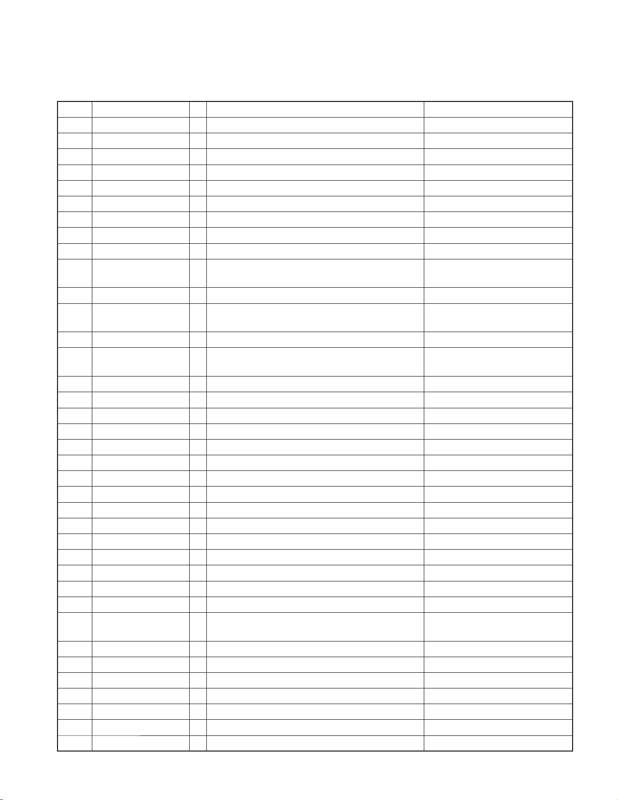
MICROCOMPUTER’S TERMINAL DESCRIPTION
SYSTEM MICROCOMPUTER: 30878MJBA22GP (X15-110: IC9)
●
Pin No. Pin Name I/O Application Processing Operation Description
1 EVOL_SDA I/O Communication data with E-VOL
1 EVOL_SDA/E2P_SDA O Communication data with E2P
2 X1 O Touch panel control
3 SIR_PON O SAT power supply ON/OFF H: ON, L: OFF
4 VSYNC_DET I Video external input detection Detects if there is VSYNC signal or not.
5 AVSW_SDA I/O Communication data with AV switch
6 AVSW_SCL O Communication clock with AV switch
7 HSY I HD input Counts HD.
8,9 NC O
10
10 TV_SC_REQ/NC O (K,R destination)
11
11 TV_MC_REQ/NC O (K,R destination)
12
12 TV_SC_CON/NC O (K,R destination)
13 INV_PWM O Inverter frequency control
14 PWIC_MUTE O Power IC output mute control H: OFF, L: ON
15 BYTE
16 CNVSS
17 XCIN
18 XCOUT
19 RESET
20 XOUT
21 VSS
22 XIN
23 VCC1
24 NMI
25 ACC_DET I ACC detection H: ACC reduced power detection
26 BU_DET I Backup power supply detection H: Backup reduced power detection
27 R_CLK/R_CLK I
27 R_CLK/NC O (X, (V) destination)
28 NC O
29 EJECT_MUTE O Mute control during loading/ejection
30 NC O
31 PWM O LCD brightness control PWM output synchronized with VSY
32 PRE_MUTEF O Pre-out mute (F/R) H: OFF, L: ON
33 BEEP O BEEP PWM output
TV_SC_REQ/TV_SC_REQ
TV_MC_REQ/TV_MC_REQ
TV_SC_CON/TV_SC_CON
Request from TV μ-com
I
(For other destination than K and R)
Request to TV μ-com
O
(For other destination than K and R)
Request to start TV μ-com
O
(For other destination than K and R)
Clock input from RDS decoder
(For other destination than X and (V))
11

KVT-50DVDRY/512/522DVD
/522DVDY/532DVD/532DVDM
MICROCOMPUTER’S TERMINAL DESCRIPTION
Pin No. Pin Name I/O Application Processing Operation Description
34 PRE_MUTESW O Pre-out mute (SW) H: OFF, L: ON
35 POWER_PWM O Frequency control of DC-DC_IC
36 NAVI_RX I Communication with navigation system
37 NAVI_TX O Communication with navigation system
38
38 TV_MC_DATA/NC O (K,R destination)
39 VCC1
40
40 TV_SC_DATA/NC O (K,R destination)
41 VSS
42
42 TV_BP_CLK/NC O (K,R destination)
43 NC O
44 TUN_SDA I/O Communication data with tuner
45 TUN_SCL O Communication clock with tuner
46 R_DATA/R_DATA I
46 R_DATA/NC O (X, (V) destination)
47 R_QUAL/R_QUAL I
47 R_QUAL/NC O (X, (V) destination)
48 EVOL_MUTE0 O E-VOL front mute L: ON, H: OFF
49 EVOL_MUTE1 O E-VOL rear mute L: ON, H: OFF
50 EVOL_MUTE2 O E-VOL C·SW mute L: ON, H: OFF
51 EVOL_MUTEB O E-VOL_B·AVOUT mute H: ON, L: OFF
52 EVOL_MUTEC O E-VOL_C mute L: ON, H: OFF
53 TV_JUDGE I Determination of TV_BOX if it is old or new H: Old, L: New
54 WRT_E2P I Used when writing into E2P
55 AVSW_PDN O Communication clock with AV switch
56 VILL_R O Brightness control of “R” in variable illumination
57 VSS
58 VILL_G O Brightness control of “G” in variable illumination
59 VCC2
60 VILL_B O Brightness control of “B” in variable illumination
61 NT_PAL I NTSC/PAL determination signal input H: PAL, L: NTSC
62 VMUTE O LCD output mute control H: MUTE, L: Normal
63 X0 O Touch panel control
64 VILL_DET I Variable illumination identifi cation terminal L: F3, H: F4
TV_MC_DATA/TV_MC_DATA
TV_SC_DATA/TV_SC_DATA
TV_BP_CLK/TV_BP_CLK
Data output to TV μ-com
O
(For other destination than K and R)
Data input from TV μ-com
I
(For other destination than K and R)
Communication clock with TV μ-com
O
(For other destination than K and R)
DATA input from RDS decoder
(For other destination than X and (V))
QUAL input from RDS decoder
(For other destination than X and (V))
L: Normal condition
H: When writing into E2P
12
KVT-50DVDRY/512/522DVD
/522DVDY/532DVD/532DVDM
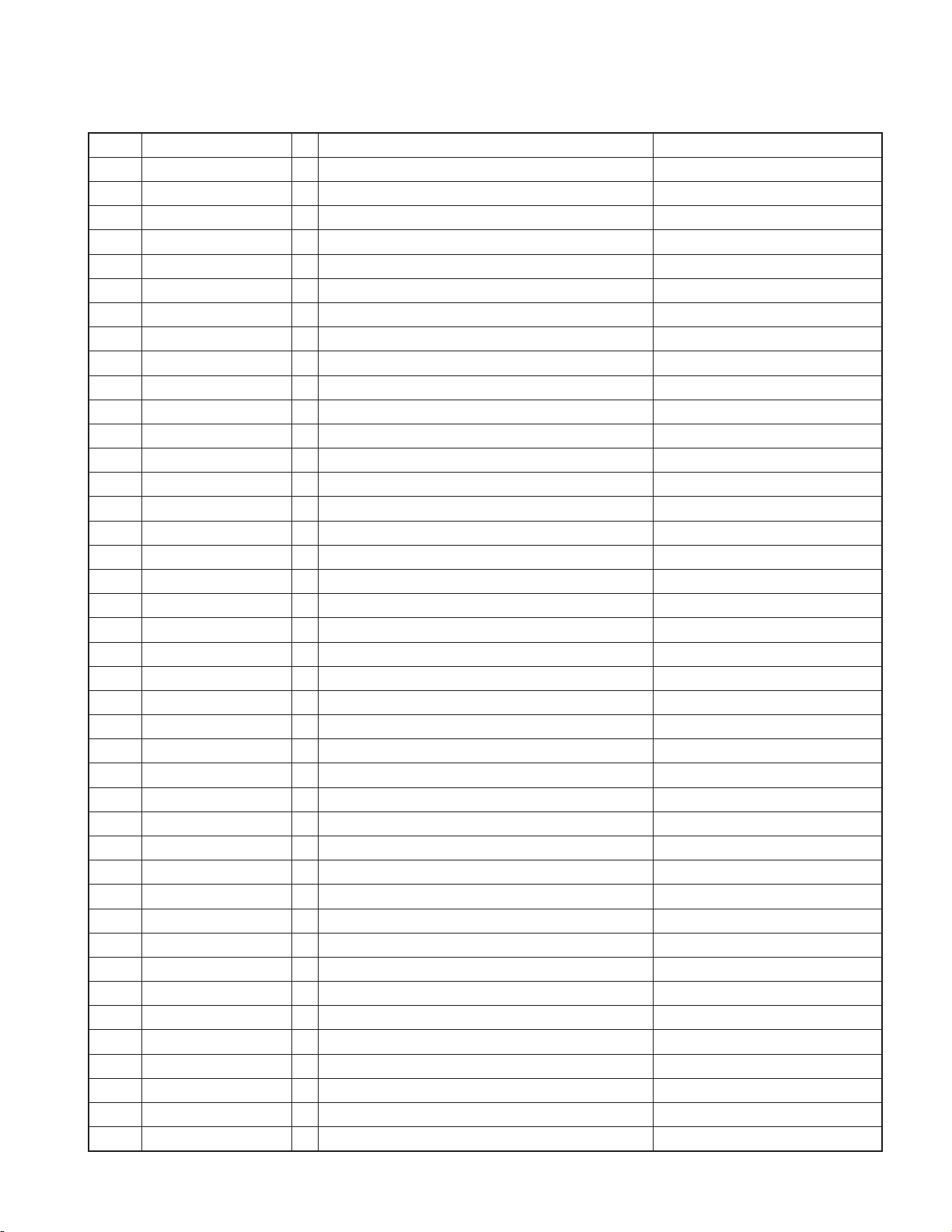
MICROCOMPUTER’S TERMINAL DESCRIPTION
Pin No. Pin Name I/O Application Processing Operation Description
65 OPEN_CLOSE I Z-MECHA OPEN/CLOSE
66 Y0 O Touch panel control
67 INV_SW O Inverter free run frequency switching
68 BL_ENA O Back light ON/OFF control H: ON, L: OFF
69 NC I Reserve
70 Z_SWT I Detection of panel mechanism
71 SW_C I Detection of panel mechanism
72 SW_B I Detection of panel mechanism
73 SW_A I Detection of panel mechanism
74 VCC2
75 SMOTOR_M O Panel mechanism slide control
76 VSS
77 SMOTOR_P O Panel mechanism slide control
78 TMOTOR_M O Panel mechanism tilt control
79 TMOTOR_P O Panel mechanism tilt control
80 AM+B O Tuner AM power supply ON/OFF control H: ON, L: OFF
81 SI O SI control L: ON, H: OFF
82 EJECT I Disk ejection
83 BE_RESET O Reset request to back end L: Reset, H: Clear reset
84 BE_RESERVE2 I Operation identifi cation terminal from back end H: Valid, L: Invalid
85 BE_STBY I Standby request from back end
86 BU_BUDET O
87 BE_INI O Initial request to back end
88 BE_SDATA I Communication data from back end
89 BE_CLK I Communication clock with back end
90 BE_MDATA O Communication data to back end
91 VCC2
92 TYPE1 I Destination settings Refer to Destination settings
93 VSS
94 TYPE2 I Destination settings Refer to Destination settings
95 BE_CON O Control request to back end
96 BE_MREQ O Request to back end
97 DISC_DET I DVD mechanism function to detect if there is a disc or not. H: There is no disc, L: There is a disc
98 NC O
99 Z_CNT I Detection of panel mechanism
100 Z_SENS I Detection of panel mechanism
101 NC O
102 VSY I VD (VSYNC) input
103 BE_RESERVE1 CLK terminal for operation identifi cation from back end CLK frequency: 1Hz
104 BE_SREQ I Request from back end
105 NC O
Notifi cation of momentary power down detection to back end
13

KVT-50DVDRY/512/522DVD
/522DVDY/532DVD/532DVDM
MICROCOMPUTER’S TERMINAL DESCRIPTION
Pin No. Pin Name I/O Application Processing Operation Description
106 ILL_G O
107 ILL_R O
108 MCNT O
109 PGOOD I DC-DC power supply error detection H: Normal, L: Error
110 P_START O DC-DC power supply ON/OFF control
111 PON O SW power supply ON/OFF control
112 NC O
113 REVERSE I Reverse detection L: Detection, H: Normal
114 PARKING I Parking detection L: Detection, H: Running
115 SIR_DET I Sirius connection detection L: Detection, H: Not-connected
116 ANT_CON O Power antenna control H: UP, L: DOWN
117 P_CON O P-CON control L: STANDBY, POWER OFF, H: EXCEPT
118 ILLUMI I Illumination detection L: ON, H: OFF
119-121
122 TYPE0 I Destination settings Refer to Destination settings
123 KEY2 I Key 2 input Refer to KEY2
124 TUN_IFC I F/E IFC input H: Station found, L: Station not found
125 TUN_SMET I S meter input
126 R_NOISE I FM noise input
127 R_AFS_H I/O Time constant switching when F/E noise is detected.
128,129
130 VSS
131 NC O
132 VCC1
133 KEY1 I Key 1 input Refer to KEY1
134 NC O
135 PWIC_STBY O Power IC standby H: ON, L: OFF
136 VCOM I For VCOM level automatic adjustment
137 X_DATA I Touch data input
138 Y_DATA I Touch data input
139 LINE_MUTE I LINE-MUTE input detection
140 AVSS
141 PWIC_DC_DET I SP output DC offset detection L: When detected
142 VREF
143 AVCC
144 EVOL_SCL/EVOL_SCL O Communication clock with E-VOL
144 EVOL_SCL/E2P_SCL O Communication clock with E2P
NC O
NC O
ON/OFF of other GREEN illumination than variable illumination
ON/OFF of other RED illumination than variable illumination
Switching of power supply voltage to the panel drive mechanism
H: ON, L: OFF
H: ON, L: OFF
H: 7.5V, L: 5V
Normal: 1.6V, TEL MUTE: 1V or less,
NAVI MUTE: 2.5V or higher
14
KVT-50DVDRY/512/522DVD
/522DVDY/532DVD/532DVDM
MICROCOMPUTER’S TERMINAL DESCRIPTION
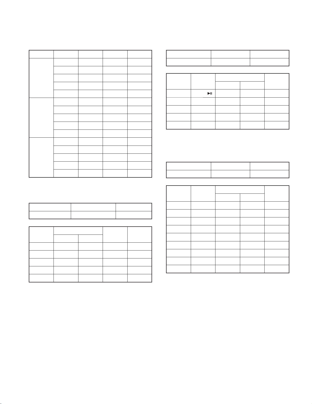
Destination settings of KVT/DDX/DNX
MODEL Destination TYPE2 TYPE1 TYPE0
K00 *
E00 *
KVT
DDX
DNX
TYPE0 is AD input.
Refer to the next table (TYPE0 Setup Voltage) for the “*”.
• TYPE0 Setup Voltage
Power supply voltage Number of destinations Pull up resistor
3.3 5 10
Destination
K 0.00 0.41 10 None
E 0.42 1.23 3.3 10
M 1.24 2.06 10 10
V/X 2.07 2.88 30 10
R 2.89 3.30 None 10
M0 0 *
V/X 0 0 *
R00 *
K01 *
E01 *
M0 1 *
V/X 0 1 *
R01 *
K11 *
E11 *
M1 1 *
V/X 1 1 *
R11 *
μ-com setup value
min max
Pull down
resistor
Pull up
resistor
KEY1 Settings
Power supply voltage Number of keys Pull up resistor
5412
Name of
key
KEY1 SCRN/ 0.00 0.69 0.2
KEY2 FNC/
KEY3 SRC/SRC 1.93 3.15 8.2
KEY4 NAV/- 3.16 4.38 24
NO KEY 4.39 5.00
When opened / When closed
When being pushed and held for a while
KEY2: TEL, KEY4: V.OFF (E), RCAM (K,R,M,X)
■
μ-com setup value
min max
0.70 1.92 3.9
Resister
value
KEY2 Settings
Power supply voltage Number of keys Pull up resistor
5812
Name of
key
KEY1 VOL- 0.00 0.42 0.3
KEY2 ATT 0.43 1.03 1.8
KEY3 VOL+ 1.04 1.64 2.2
KEY4 AUTO 1.65 2.25 3.3
KEY5 AM 2.26 2.86 5.1
KEY6 FM 2.87 3.47 8.2
KEY7
KEY8 SEEK UP 4.09 4.69 51
NO KEY 4.70 5.00
When being pushed and held for a while
KEY2: LOUD (K,R,X)
SEEK DOWN
μ-com setup value
min max
3.48 4.08 16
Resister
value
15
KVT-50DVDRY/512/522DVD
/522DVDY/532DVD/532DVDM
ADJUSTMENT
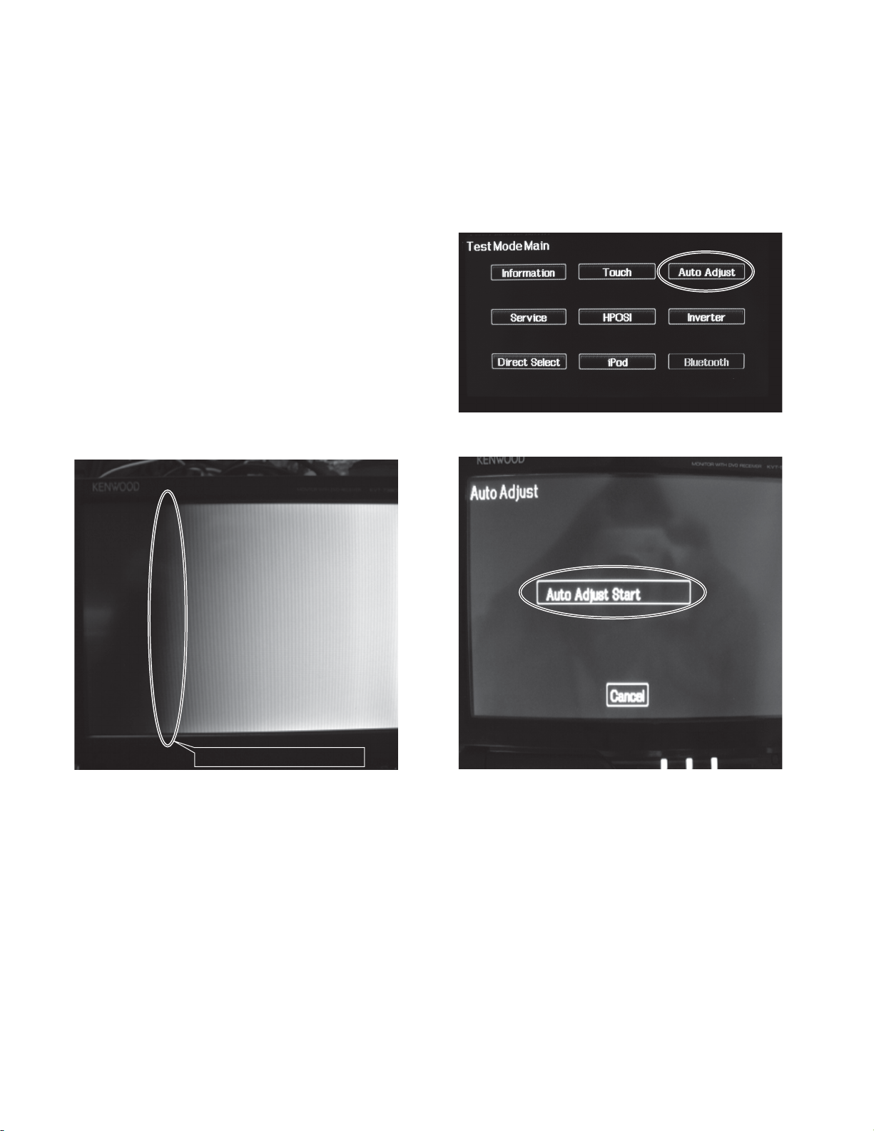
1. Flicker adjustment
Condition
●
Video source: VIDEO
Video: RAMP
BRIGHT: MAX
MODE: FULL
Adjustment procedure
●
Display RAMP.
q
Rotate VR200: X35-496 until the leading edge of black
w
area reaches far right of the screen. As shown in the
next picture, the edge is now located at about 1/5 of the
screen width from the left of the screen. (At the comple-
tion of this adjustment, most of the screen will be in
black.)
The position where the adjustment is best completed
can be shown darkest and clearest.
2. VCOM Amplitude and AGC and WB
Automatic adjustments
Adjustment Method
●
Input 100% (white) in AV-IN.
q
Press Auto Adjust on the Test Mode Main screen.
w
Press Auto Adjust Start.
e
Adjust it by confirming this area
Example: Keep rotating the VR200 so that the black area
is gradually expanded (to the right), and if you rotate the
VR200 too much, the black area will start shrinking. So
when you see the black area starts shrinking, rotate the
VR200 backward a bit to make the adjustment relatively
stable.
16
After the automatic adjustment, “Auto Set OK” will be
r
shown to indicate the completion of the adjustment.
ADJUSTMENT
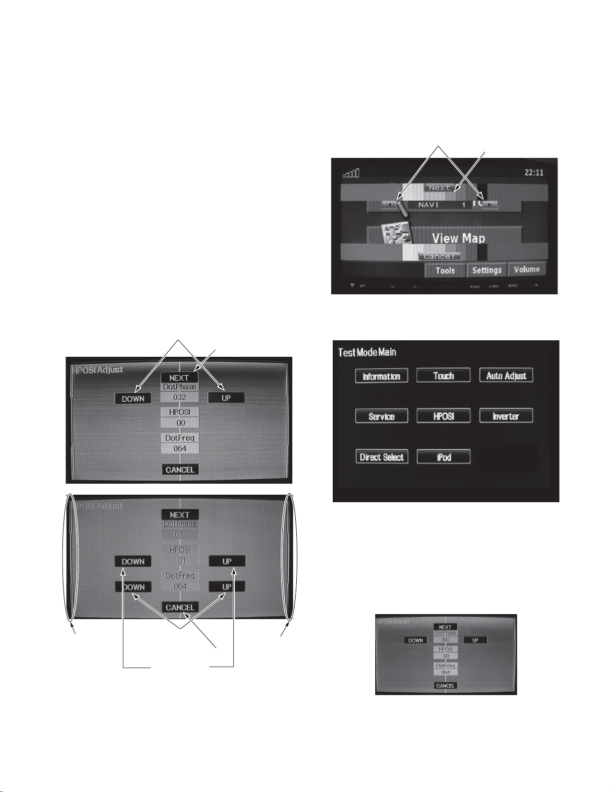
3. Adjustment of Horizontal display start
position and pixel
Video displayed on Adjustment screen
●
GRAPHIC: Special screen used only for adjustment (See
below)
NAVI: Input KNA-DV3200 or KNA-G520
Default Value
●
Pixel Adjustment key (DOT_PHASE): Adjustment of hori-
zontal display position of pixel (Default: 32)
Screen Position Adjustment key (HPOSI): Adjustment of
horizontal display starting position of the entire screen
(Default: 0)
Display Range Adjustment key (DOT_FREQ): Adjustment
of horizontal display range of the video (Default: 64)
KVT-50DVDRY/512/522DVD
/522DVDY/532DVD/532DVDM
NAVI Adjustment screen
●
Adjustment screen changes depending on what type
(model) of NAVI is connected.
Screen Position
Adjustment key
Proceed to the next
adjustment screen
GRAPHIC Adjustment screen
●
Pixel Adjustment key
Proceed to the next
adjustment screen.
Adjustment Procedure
●
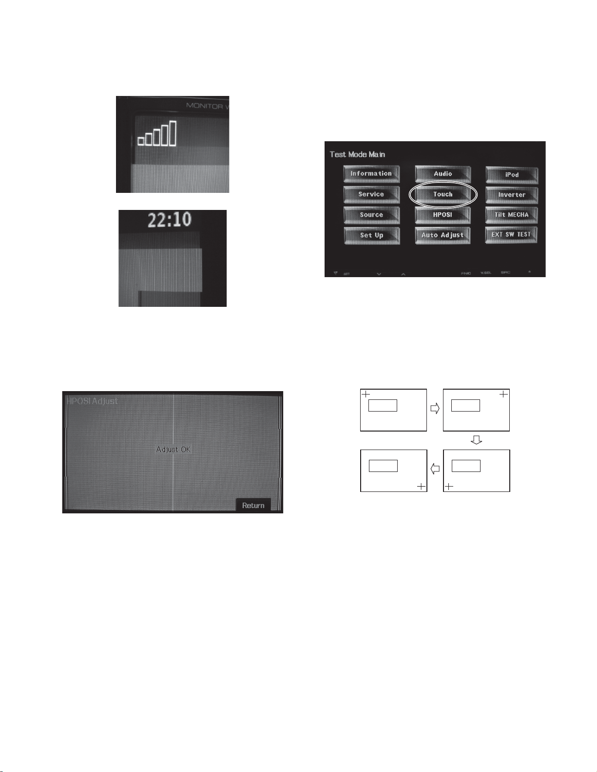
Press HPOSI on the Test Mode Main screen.
q
-1 Grafhic (DotPhase)
w
Then, adjust the Pixel Adjustment key so that the screen
becomes gray.
After the completion of the adjustment, press “NEXT”.
• Pixel Adjustment: GRAPHIC
OK
Horizontal
Screen Position
Adjustment OSD
Display Range
Adjustment key
Return to the Menu
Screen Position
Adjustment key
Horizontal
Screen Position
Adjustment OSD
17
KVT-50DVDRY/512/522DVD
/522DVDY/532DVD/532DVDM
ADJUSTMENT
NG
Enlarge OK
Enlarge NG
NG
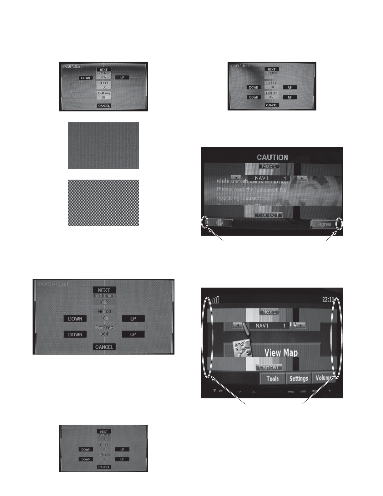
-2-1 NAVI (In case of KNA-DV3200)
w
Adjust the Screen Adjustment key so that the NAVI
screen becomes horizontally symmetrical.
-2 Grafhic (HPOSI)
w
Adjust the Screen Adjustment key so that the screen be-
comes horizontally symmetrical.
• Screen Position Adjustment: GRAPHIC
-3 Grafhic (DotFreq)
w
Then, adjust the Display Range Adjustment key so that
there is no vertical black stripes (blur) on the screen.
After the completion of the adjustment, press “NEXT”.
• Adjustment of display range: GRAPHIC
OK
Adjust the screen such that KEY (gap) at the
right and left sides becomes symmetrical.
-2-2 NAVI (In case of KNA-G520)
w
Adjust the Screen Adjustment key so that the NAVI
screen becomes horizontally symmetrical.
Adjust the space to become horizontal symmetry
18
ADJUSTMENT
KVT-50DVDRY/512/522DVD
/522DVDY/532DVD/532DVDM
Enlarge OK
Enlarge OK
Confi rmation after adjustment
●
After the adjustment, check that the screen is horizon-
tally symmetrical and that there is no blur on the screen.
The “HPOSI OK” will be shown to indicate the comple-
tion of the adjustment.
4. Touch panel adjustment
Adjustment procedure
●
Press the Touch Key on the Test Mode Menu screen to
q
enter the Touch panel adjustment screen.
Touch the center of “+” mark below in the following or-
w
der.
Upper left → Upper right → Lower left → Lower right
To touch, make sure to use the designated touch stick.
After adjustment is completed for 4 areas, if “Write OK”
e
is displayed, the adjustment is completed.
Press Return to exit from the Touch screen.
Cancel Cancel
CancelCancel
∗ If the center of “+” mark wasn’t pressed accurately, press
Cancel to start over the adjustment.
Note
The touch panel adjustment data is finalized when the
touch stick is released from the mark.
Therefore, the Knack for Adjustment is not to release the
touch stick from the mark right after touching the center
of the “+” mark, but to confi rm that the stick is exactly
on the center of the “+” mark while keeping touching the
screen. (If the stick is not exactly on the center of the
mark, move the stick onto the center of the mark while
keeping touching the screen.)
Then, quickly and vertically release the stick from the
screen.
19
A B C D E
1
R
C89
R
Q
C
KVT-50DVDRY/512/522DVD
/522DVDY/532DVD/532DVDM
1
2
3
4
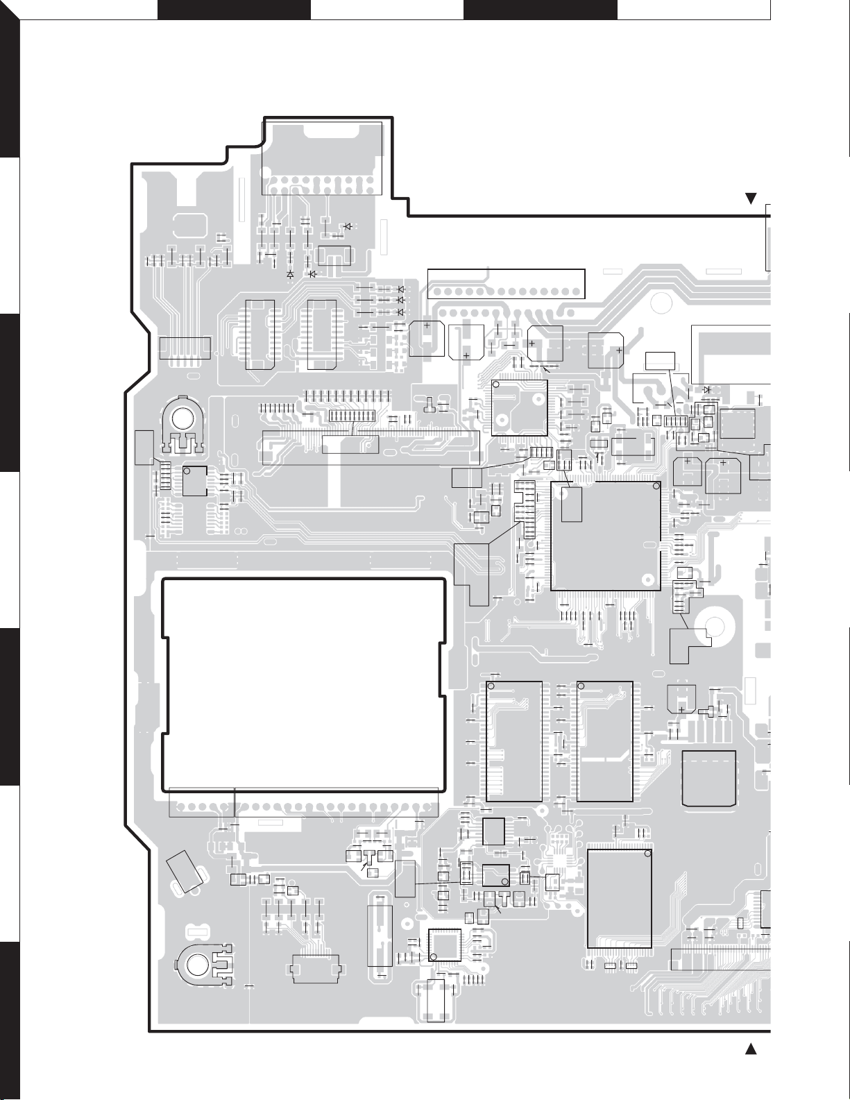
PC BOARD (COMPONENT SIDE VIEW)
VIDEO CONTROL UNIT
X15-110x-xx A/2
(J76-0505-12)
R543
C494
R512
R513
R544
C495
R503
R502
R501
C203
C389
D376
R511
R510
D375
R406
CN352
P2
1
D374
IC361
D373
15
R489
C455
R405
16
C497
R515
C499
R548
98
C385
C496
C498
D372
R404
R516
R517
D370
R403
D371
D369
20
19
R402
R400
R401
R385
C377
R386
C376
R390
C378
CN351
R394
D366
D365
202
CN355
C150
R518
R519
202
191
CN354
D21
D19
D20
C153
C155
C154
F2
C151
C152
C156
C157
168
21
D22
R159
R160
D367
D23
R161
C379
191
R162
D31
R163
CN2
R452
R454
R428
D30
R164
R453
D29
R165
2
1
D28
R166
CN3
R439
R167
C424
C423
C425
D27
R168
D25
C162
C161
D384
R438
D24
D413
D396
D401
R170
R171
D32
1
2
C352
C164
C163
C470
R269
R283
R244
R243
R272
R492
C473
C457
C474
R482
R481
R480
R242
R241
R240
R239
R270
R271
R238
R273
R284
R237
R274
C459
C465
C462
L451
BE
C380
1
16
C463
Q451
C735
IC351
C356
C353
C383
C471
C469
C472
64 49
IC358
17 32
C460
C467
C468
Q453
R493
R494
C466
C464
EB
Q452
L361
C500
R276
R288
R280
R275
R236
R286
C456
33
37
C192
C191
72
C188
C454
48
27
26
C11
C28
R245
R246
R248
R266
R488
C477
C479
C478
C482
C480
C476
C443
C475
R495
C481
R252
BE
36
R253
R267
R268
R265
R282
R216
Q78
R264
GS
D
X2
C196
R224
R263
D
GS
R262
Q79
C194
C193
Q39
IC9
C187
R222
R223
R215
R227
R247
BE
R73
R250
G
S
R251
D
Q76
R260
R259
R258
X1
1
144
C186
109
10873
R221
R213
R214
R256
C19
C189
R255
C184
R234
C190
R233
R229
R232
R211
R231
C26
R47
B
R208
R210
R228
Q77
BE
D14
R48
R46
E
B
C18
Q23
R254
R123
R49
R235
R281
R50
L2
EB
BE
E
EB
L12
L13
R220
R218
R219
R217
R249
R279
C752
1
5
18151
C392
CN357 CN356
C397
6
W351
L355
Q362
R185
BE
C359
R412
C173
D34
R411
R183
D36
EB
B
Q80
E
R184
R187
R186
D37
D35
111
CN4
Q361
P5
D41
R188
R370
Q373
D368
C431
R361R354
BE
Q371
X351
C384
C406
C407
C390
R364
BE
Q372
R677
C664
C673
EB
R664
Q654
C666
R674
R666
C229
R673
C672
30
31
R846
R847
C855
40
R831
C852
L851
C851
R848
C853
IC851
1
EB
X851
R652
R653
R654
R676
EB
C751
21
10
C756
C655
C662
R662
C668
Q655
R832
C854
C754
C755
R885
Q683
20
11
R833
R670
R840
C753
R668
BE
R837
27
C657
C661
5
8
BE
R834
R844
R843
R838
R835
IC651
IC652
BE
R845
R836
L751
R841
Q653
IC704
161
98
4
Q652
R651
1
BE
D651
C658
R661
Q651
C656
C663
R663
R669
C667
R667
54
28
C741
R763
C742
C743
C758
C744
C757
R884
C746
C665
1
C745
L741
R665
R225
IC703
L731
C731
24 1
IC702
CP751
R762
R883
C732
R278
54
2827
C748
C747
R764
R761
CP752
R760
4825
R230
R206
R207
C183
R205
R204
C703
L703
R769
C762
C764
C185
L702
D701
C702
R702
51
R770
IC705
CP753
C761
C763
1
C704
R157
R156
L3
R
11
I
20
CN701
R212
7
20
 Loading...